US7339228B2 - Non-planar flash memory array with shielded floating gates on silicon mesas - Google Patents
Non-planar flash memory array with shielded floating gates on silicon mesasDownload PDFInfo
- Publication number
- US7339228B2 US7339228B2US11/363,730US36373006AUS7339228B2US 7339228 B2US7339228 B2US 7339228B2US 36373006 AUS36373006 AUS 36373006AUS 7339228 B2US7339228 B2US 7339228B2
- Authority
- US
- United States
- Prior art keywords
- substrate
- floating gates
- forming
- trenches
- insulator layer
- Prior art date
- Legal status (The legal status is an assumption and is not a legal conclusion. Google has not performed a legal analysis and makes no representation as to the accuracy of the status listed.)
- Expired - Fee Related, expires
Links
- 230000015654memoryEffects0.000titleclaimsabstractdescription74
- 238000007667floatingMethods0.000titleclaimsabstractdescription61
- 229910052710siliconInorganic materials0.000titleclaimsdescription16
- 239000010703siliconSubstances0.000titleclaimsdescription16
- XUIMIQQOPSSXEZ-UHFFFAOYSA-NSiliconChemical compound[Si]XUIMIQQOPSSXEZ-UHFFFAOYSA-N0.000titledescription15
- 229910052751metalInorganic materials0.000claimsabstractdescription22
- 239000002184metalSubstances0.000claimsabstractdescription22
- 239000000758substrateSubstances0.000claimsdescription54
- 238000000034methodMethods0.000claimsdescription50
- 239000012212insulatorSubstances0.000claimsdescription35
- VYPSYNLAJGMNEJ-UHFFFAOYSA-NSilicium dioxideChemical compoundO=[Si]=OVYPSYNLAJGMNEJ-UHFFFAOYSA-N0.000claimsdescription14
- KWYUFKZDYYNOTN-UHFFFAOYSA-MPotassium hydroxideChemical compound[OH-].[K+]KWYUFKZDYYNOTN-UHFFFAOYSA-M0.000claimsdescription13
- GWEVSGVZZGPLCZ-UHFFFAOYSA-NTitan oxideChemical compoundO=[Ti]=OGWEVSGVZZGPLCZ-UHFFFAOYSA-N0.000claimsdescription12
- 238000000151depositionMethods0.000claimsdescription12
- 238000001704evaporationMethods0.000claimsdescription11
- MCMNRKCIXSYSNV-UHFFFAOYSA-NZirconium dioxideChemical compoundO=[Zr]=OMCMNRKCIXSYSNV-UHFFFAOYSA-N0.000claimsdescription10
- 238000005530etchingMethods0.000claimsdescription10
- 230000008020evaporationEffects0.000claimsdescription10
- 229910021420polycrystalline siliconInorganic materials0.000claimsdescription10
- 229920005591polysiliconPolymers0.000claimsdescription10
- 238000000231atomic layer depositionMethods0.000claimsdescription8
- 230000008021depositionEffects0.000claimsdescription8
- 230000003647oxidationEffects0.000claimsdescription8
- 238000007254oxidation reactionMethods0.000claimsdescription8
- 239000003989dielectric materialSubstances0.000claimsdescription7
- 150000004767nitridesChemical class0.000claimsdescription7
- CJNBYAVZURUTKZ-UHFFFAOYSA-Nhafnium(IV) oxideInorganic materialsO=[Hf]=OCJNBYAVZURUTKZ-UHFFFAOYSA-N0.000claimsdescription6
- -1CrTiO3Inorganic materials0.000claimsdescription5
- 229910002244LaAlO3Inorganic materials0.000claimsdescription5
- 238000001465metallisationMethods0.000claimsdescription5
- 229910018557Si OInorganic materials0.000claimsdescription4
- CMIHHWBVHJVIGI-UHFFFAOYSA-Ngadolinium(III) oxideInorganic materials[O-2].[O-2].[O-2].[Gd+3].[Gd+3]CMIHHWBVHJVIGI-UHFFFAOYSA-N0.000claimsdescription4
- LIVNPJMFVYWSIS-UHFFFAOYSA-Nsilicon monoxideInorganic materials[Si-]#[O+]LIVNPJMFVYWSIS-UHFFFAOYSA-N0.000claimsdescription4
- RUDFQVOCFDJEEF-UHFFFAOYSA-Nyttrium(III) oxideInorganic materials[O-2].[O-2].[O-2].[Y+3].[Y+3]RUDFQVOCFDJEEF-UHFFFAOYSA-N0.000claimsdescription4
- 229910017107AlOxInorganic materials0.000claimsdescription2
- 229910003074TiCl4Inorganic materials0.000claimsdescription2
- 229910010386TiI4Inorganic materials0.000claimsdescription2
- 229910003087TiOxInorganic materials0.000claimsdescription2
- 229910003077Ti−OInorganic materials0.000claimsdescription2
- 229910006252ZrONInorganic materials0.000claimsdescription2
- 229910003134ZrOxInorganic materials0.000claimsdescription2
- 239000002131composite materialSubstances0.000claimsdescription2
- 229910052814silicon oxideInorganic materials0.000claimsdescription2
- HLLICFJUWSZHRJ-UHFFFAOYSA-NtioxidazoleChemical compoundCCCOC1=CC=C2N=C(NC(=O)OC)SC2=C1HLLICFJUWSZHRJ-UHFFFAOYSA-N0.000claimsdescription2
- XJDNKRIXUMDJCW-UHFFFAOYSA-Jtitanium tetrachlorideChemical compoundCl[Ti](Cl)(Cl)ClXJDNKRIXUMDJCW-UHFFFAOYSA-J0.000claimsdescription2
- NLLZTRMHNHVXJJ-UHFFFAOYSA-Jtitanium tetraiodideChemical compoundI[Ti](I)(I)INLLZTRMHNHVXJJ-UHFFFAOYSA-J0.000claimsdescription2
- 239000010410layerSubstances0.000description28
- 239000010408filmSubstances0.000description19
- 238000004519manufacturing processMethods0.000description9
- 230000008878couplingEffects0.000description7
- 238000010168coupling processMethods0.000description7
- 238000005859coupling reactionMethods0.000description7
- 238000010849ion bombardmentMethods0.000description7
- 239000002243precursorSubstances0.000description6
- 239000004065semiconductorSubstances0.000description6
- 239000000377silicon dioxideSubstances0.000description6
- 238000002347injectionMethods0.000description5
- 239000007924injectionSubstances0.000description5
- 239000001301oxygenSubstances0.000description5
- 229910052760oxygenInorganic materials0.000description5
- 238000002207thermal evaporationMethods0.000description5
- 229910052727yttriumInorganic materials0.000description5
- 229910052688GadoliniumInorganic materials0.000description4
- QVGXLLKOCUKJST-UHFFFAOYSA-Natomic oxygenChemical compound[O]QVGXLLKOCUKJST-UHFFFAOYSA-N0.000description4
- 238000005566electron beam evaporationMethods0.000description4
- 238000005516engineering processMethods0.000description4
- 239000002784hot electronSubstances0.000description4
- 239000000463materialSubstances0.000description4
- 239000010409thin filmSubstances0.000description4
- 238000006243chemical reactionMethods0.000description3
- 238000004544sputter depositionMethods0.000description3
- XKRFYHLGVUSROY-UHFFFAOYSA-NArgonChemical compound[Ar]XKRFYHLGVUSROY-UHFFFAOYSA-N0.000description2
- MHAJPDPJQMAIIY-UHFFFAOYSA-NHydrogen peroxideChemical compoundOOMHAJPDPJQMAIIY-UHFFFAOYSA-N0.000description2
- GQPLMRYTRLFLPF-UHFFFAOYSA-NNitrous OxideChemical compound[O-][N+]#NGQPLMRYTRLFLPF-UHFFFAOYSA-N0.000description2
- CBENFWSGALASAD-UHFFFAOYSA-NOzoneChemical compound[O-][O+]=OCBENFWSGALASAD-UHFFFAOYSA-N0.000description2
- 230000006978adaptationEffects0.000description2
- PNEYBMLMFCGWSK-UHFFFAOYSA-Naluminium oxideInorganic materials[O-2].[O-2].[O-2].[Al+3].[Al+3]PNEYBMLMFCGWSK-UHFFFAOYSA-N0.000description2
- 238000010276constructionMethods0.000description2
- 229910052593corundumInorganic materials0.000description2
- 238000010586diagramMethods0.000description2
- 230000000694effectsEffects0.000description2
- 150000002500ionsChemical class0.000description2
- 238000002955isolationMethods0.000description2
- MRELNEQAGSRDBK-UHFFFAOYSA-Nlanthanum oxideInorganic materials[O-2].[O-2].[O-2].[La+3].[La+3]MRELNEQAGSRDBK-UHFFFAOYSA-N0.000description2
- 239000011159matrix materialSubstances0.000description2
- 239000000203mixtureSubstances0.000description2
- KTUFCUMIWABKDW-UHFFFAOYSA-Noxo(oxolanthaniooxy)lanthanumChemical compoundO=[La]O[La]=OKTUFCUMIWABKDW-UHFFFAOYSA-N0.000description2
- 239000008188pelletSubstances0.000description2
- 235000012239silicon dioxideNutrition0.000description2
- 238000003860storageMethods0.000description2
- 230000005641tunnelingEffects0.000description2
- 229910001845yogo sapphireInorganic materials0.000description2
- JBRZTFJDHDCESZ-UHFFFAOYSA-NAsGaChemical compound[As]#[Ga]JBRZTFJDHDCESZ-UHFFFAOYSA-N0.000description1
- OKTJSMMVPCPJKN-UHFFFAOYSA-NCarbonChemical compound[C]OKTJSMMVPCPJKN-UHFFFAOYSA-N0.000description1
- 206010021143HypoxiaDiseases0.000description1
- 150000001298alcoholsChemical class0.000description1
- 229910045601alloyInorganic materials0.000description1
- 239000000956alloySubstances0.000description1
- 229910052786argonInorganic materials0.000description1
- 230000015572biosynthetic processEffects0.000description1
- 239000006227byproductSubstances0.000description1
- 229910052799carbonInorganic materials0.000description1
- 230000001413cellular effectEffects0.000description1
- 238000010549co-EvaporationMethods0.000description1
- 238000004891communicationMethods0.000description1
- 238000011109contaminationMethods0.000description1
- 239000013078crystalSubstances0.000description1
- 238000010894electron beam technologyMethods0.000description1
- 238000000313electron-beam-induced depositionMethods0.000description1
- 238000011066ex-situ storageMethods0.000description1
- 230000005284excitationEffects0.000description1
- 230000002349favourable effectEffects0.000description1
- 230000006870functionEffects0.000description1
- 239000007789gasSubstances0.000description1
- 229910052732germaniumInorganic materials0.000description1
- GNPVGFCGXDBREM-UHFFFAOYSA-Ngermanium atomChemical compound[Ge]GNPVGFCGXDBREM-UHFFFAOYSA-N0.000description1
- 238000010438heat treatmentMethods0.000description1
- 238000002513implantationMethods0.000description1
- 239000011261inert gasSubstances0.000description1
- 238000010884ion-beam techniqueMethods0.000description1
- 229910052743kryptonInorganic materials0.000description1
- DNNSSWSSYDEUBZ-UHFFFAOYSA-Nkrypton atomChemical compound[Kr]DNNSSWSSYDEUBZ-UHFFFAOYSA-N0.000description1
- 229910052746lanthanumInorganic materials0.000description1
- 230000000873masking effectEffects0.000description1
- 150000002739metalsChemical class0.000description1
- 239000001272nitrous oxideSubstances0.000description1
- 238000005498polishingMethods0.000description1
- 238000010926purgeMethods0.000description1
- 238000000746purificationMethods0.000description1
- 238000004151rapid thermal annealingMethods0.000description1
- 229910052594sapphireInorganic materials0.000description1
- 239000010980sapphireSubstances0.000description1
- 239000002356single layerSubstances0.000description1
- 239000007858starting materialSubstances0.000description1
- 239000000126substanceSubstances0.000description1
- 230000001360synchronised effectEffects0.000description1
- 238000009827uniform distributionMethods0.000description1
- XLYOFNOQVPJJNP-UHFFFAOYSA-NwaterSubstancesOXLYOFNOQVPJJNP-UHFFFAOYSA-N0.000description1
- VWQVUPCCIRVNHF-UHFFFAOYSA-Nyttrium atomChemical compound[Y]VWQVUPCCIRVNHF-UHFFFAOYSA-N0.000description1
Images


Classifications
- G—PHYSICS
- G11—INFORMATION STORAGE
- G11C—STATIC STORES
- G11C16/00—Erasable programmable read-only memories
- G11C16/02—Erasable programmable read-only memories electrically programmable
- G11C16/04—Erasable programmable read-only memories electrically programmable using variable threshold transistors, e.g. FAMOS
- G11C16/0408—Erasable programmable read-only memories electrically programmable using variable threshold transistors, e.g. FAMOS comprising cells containing floating gate transistors
- H—ELECTRICITY
- H10—SEMICONDUCTOR DEVICES; ELECTRIC SOLID-STATE DEVICES NOT OTHERWISE PROVIDED FOR
- H10B—ELECTRONIC MEMORY DEVICES
- H10B41/00—Electrically erasable-and-programmable ROM [EEPROM] devices comprising floating gates
- H10B41/20—Electrically erasable-and-programmable ROM [EEPROM] devices comprising floating gates characterised by three-dimensional arrangements, e.g. with cells on different height levels
- H10B41/23—Electrically erasable-and-programmable ROM [EEPROM] devices comprising floating gates characterised by three-dimensional arrangements, e.g. with cells on different height levels with source and drain on different levels, e.g. with sloping channels
- H—ELECTRICITY
- H10—SEMICONDUCTOR DEVICES; ELECTRIC SOLID-STATE DEVICES NOT OTHERWISE PROVIDED FOR
- H10B—ELECTRONIC MEMORY DEVICES
- H10B41/00—Electrically erasable-and-programmable ROM [EEPROM] devices comprising floating gates
- H10B41/30—Electrically erasable-and-programmable ROM [EEPROM] devices comprising floating gates characterised by the memory core region
- H10B41/35—Electrically erasable-and-programmable ROM [EEPROM] devices comprising floating gates characterised by the memory core region with a cell select transistor, e.g. NAND
Definitions
- the present inventionrelates generally to memory devices and in particular the present invention relates to a flash memory devices.
- RAMrandom-access memory
- ROMread only memory
- DRAMdynamic random access memory
- SDRAMsynchronous dynamic random access memory
- flash memoryflash memory
- Flash memory deviceshave developed into a popular source of non-volatile memory for a wide range of electronic applications. Flash memory devices typically use a one-transistor memory cell that allows for high memory densities, high reliability, and low power consumption. Common uses for flash memory include personal computers, personal digital assistants (PDAs), digital cameras, and cellular telephones. Program code and system data such as a basic input/output system (BIOS) are typically stored in flash memory devices for use in personal computer systems.
- BIOSbasic input/output system
- Stray capacitance in flash memory cellscan cause problems. For example, the capacitance between different floating gates that are close together can cause coupling and cross-talk between the floating gates of neighboring cells. This may also have the effect of reducing memory cell performance.
- FIG. 1illustrates a cross-sectional view of a typical prior art memory cell array.
- a typical cellis comprised of a silicon substrate 100 .
- a gate insulator layer 101is formed on top of the substrate 100 .
- Oxide isolation areas 103 and 104are formed between the cells.
- the floating gates 105 and 106are formed between the oxide isolation areas 103 and 104 .
- An interpoly insulator 107is formed over the floating gates 105 and 106 prior to forming the control gate 110 on top.
- the memory arrayis comprised of multiple rows 120 and 121 of memory cell transistors.
- C A-DThe capacitances that couple the various components of the array are illustrated as C A-D .
- C Ais the row-to-row floating gate stray capacitance.
- C Bis the end-to-end floating gate stray capacitance.
- C Cis the floating gate-to-control gate coupling capacitance and
- C Dis the floating gate-to-substrate coupling capacitance.
- the ratio of these capacitive componentsis determined by the geometrical dimensions of the facing surfaces constituting the capacitance and the dielectric constants of the insulator materials.
- the ends and sides of the floating gatesare the plate areas of the stray capacitances.
- the dielectrics between the side and end areasare the oxide and have the same dielectric constant as the gate oxide.
- the polysilicon floating gate materialis thick resulting in large surfaces on the ends and sides of the floating gates. The thick floating gate material results in greater stray capacitances.
- the present inventionencompasses a non-planar flash memory array comprised of memory cells on mesas. Each memory cell has a floating gate and a control gate coupled to a wordline.
- the arraycomprises a plurality of columns of memory cells are fabricated in multiple planes of a substrate. A plurality of rows of memory cells are fabricated in the multiple planes. The memory cells of each row are coupled through a wordline. A metal layer is formed between and substantially parallel to adjacent wordlines such that the floating gates of adjacent memory cells are shielded.
- FIG. 1shows a cross-sectional view, along a wordline, of a typical prior art NAND flash memory cell array.
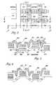
- FIG. 2shows a top view of one embodiment of a flash memory array of the present invention with shielded floating gates on silicon mesas.
- FIG. 3shows a cross-sectional view along axis A-A′ of the embodiment of FIG. 2 .
- FIG. 4shows a cross-sectional view along axis B-B′ of the embodiment of FIG. 2 .
- FIG. 5shows a cross-sectional view along axis C-C′ of the embodiment of FIG. 2 .
- FIG. 6shows a cross-sectional view of fabrication steps for one embodiment of the present invention in accordance with the array of FIG. 2 .
- FIG. 7shows a cross-sectional view of additional steps for one embodiment of the fabrication method of the present invention in accordance with the array of FIG. 2 .
- FIG. 8shows a cross-sectional view of additional steps for one embodiment of the fabrication method of the present invention in accordance with the array of FIG. 2 .
- FIG. 9shows a cross-sectional view of additional steps for one embodiment of the fabrication method of the present invention in accordance with the array of FIG. 2 .
- FIG. 10shows a cross-sectional view of additional steps for one embodiment of the fabrication method of the present invention in accordance with the array of FIG. 2 .
- FIG. 11shows a cross-sectional view of an alternate embodiment of the flash memory array of the present invention.
- FIG. 12shows a block diagram of an electronic system of the present invention that incorporates the memory array of FIG. 2 .
- GaAsgallium arsenide
- SOSsilicon-on-sapphire
- SOIsilicon-on-insulator
- TFTthin film transistor
- doped and undoped semiconductorsepitaxial layers of a silicon supported by a base semiconductor structure, as well as other semiconductor structures well known to one skilled in the art.
- wafer or substratewhen reference is made to a wafer or substrate in the following description, previous process steps may have been utilized to form regions/junctions in the base semiconductor structure, and terms wafer or substrate include the underlying layers containing such regions/junctions.
- the present inventionis not limited to such an architecture.
- the flash memory array with shielded floating gatescan be fabricated in a NOR architecture.
- each floating gate memory cell of the array matrixis connected by rows to wordlines and their drains are connected to column bitlines.
- the source of each floating gate memory cellis typically connected to a common source line. Still other embodiments can use other architectures.
- FIG. 2illustrates a top view of one embodiment of a flash memory array of the present invention with shielded floating gates on silicon mesas.
- the transistorsare formed both on the mesas and in adjacent valleys between the mesas.
- Metal shieldingprevents coupling between adjacent floating gates in the same column.
- Wordlines that connect the rows of the arrayare formed into the valleys between adjacent columns to prevent coupling between floating gates in the adjacent columns.
- FIG. 2illustrates cross-sectional axes that are used to show the structures of the present invention.
- a cross-sectional view along axis A-A′ of one embodiment of the present inventionis illustrated in FIG. 3 .
- a cross-sectional view along axis B-B′ of one embodiment of the present inventionis illustrated in FIG. 4 .
- a cross-sectional view along axis C-C′ of one embodiment of the present inventionis illustrated in FIG. 5 .
- FIG. 3illustrates a cross-sectional view along axis A-A′ of the embodiment of FIG. 2 .
- the memory cellsare fabricated on a mesa and valley surface with transistors fabricated both on the mesas and in the valleys.
- the cellsare not vertical structures but are conventional devices with conduction in channels that are parallel to the substrate surface.
- the portion of the array illustrated in FIG. 3is comprised of a column of cells of which two 330 and 332 are discussed.
- One cell 330is fabricated in a valley while the other cell 332 is fabricated on a mesa.
- the cells 332 on the mesasmay be considered to be formed on an upper plane of the substrate and the cells 330 in the valleys may be considered to be formed in a lower plane of the substrate.
- Source/drain regions 308 - 310are doped into the sides of the mesas. These regions 308 - 310 couple adjacent cells (e.g., cell 330 to 332 ) of each plane together into columns of a NAND architecture. A channel region exists at the top of each mesa and the bottom of each valley such that, during operation of the cells 330 and 332 , a channel forms in the channel region between each pair of source/drain regions 308 and 309 or 309 and 310 .
- the source/drain regions 308 - 310are n+ regions that are doped into a p-type substrate.
- the source/drain regions and substrate of the present inventionare not limited to any one conductivity type.
- Gate insulator layers 320 and 321are formed over the channel regions and between the source/drain regions 308 and 309 or 309 and 310 .
- Floating gates 322 and 323are formed over the gate insulators 320 and 321 . In one embodiment, these are polysilicon floating gates. Alternate embodiments may use nitride or other types of charge storage layers.
- Intergate insulator layers 324 and 325are formed over the floating gate layers 322 and 323 respectively.
- Control gates 326 and 327are formed over the intergate insulators 324 and 325 respectively.
- the control gates 326 and 327are coupled to, or are part of, the wordlines of the memory array as illustrated in subsequent figures showing different cross-sectional areas.
- the wordlinescouple the rows of the array by following the mesa/valley structure.
- a metal layer 350 - 352is formed between adjacent wordlines in a column of cells of the memory array.
- the metal 350 - 352extends along the rows substantially parallel to the wordlines to shield the floating gates 322 and 323 of the adjacent cells 330 and 332 .
- the metal 350 - 352is formed deep enough into the structure such that the floating gates on the mesas are shielded from the lower floating gates in the valleys.
- the metal shieldscan be formed after oxidation of the wordlines and by a metal deposition process.
- the gate insulator layer and intergate insulator layer between the polysilicon gates, as illustrated in FIG. 3can be high-k dielectrics (i.e., dielectric constant greater than that of SiO 2 ), composite insulators, silicon oxide, or some other insulator.
- Silicon dioxide (SiO 2 )is an insulator with a relative dielectric constant of 3.9.
- a high-k gate insulatorrequires smaller write and erase voltages due to the reduced thickness layer between the control gate and the floating gate.
- These dielectric layersmay be formed by atomic layer deposition (ALD), evaporation, or some other fabrication technique.
- ALDis based on the sequential deposition of individual monolayers or fractions of a monolayer in a well-controlled manner. Gaseous precursors are introduced one at a time to the substrate surface and between the pulses the reactor is purged with an inert gas or evacuated.
- the precursoris saturatively chemisorbed at the substrate surface and during subsequent purging the precursor is removed from the reactor.
- another precursoris introduced on the substrate and the desired films growth reaction takes place. After that reaction, byproducts and the precursor excess are purged from the reactor.
- one ALD cyclecan be performed in less than one second in a properly designed flow-type reactor.
- the most commonly used oxygen source materials for ALDare water, hydrogen peroxide, and ozone. Alcohols, oxygen and nitrous oxide can also been used.
- ALDis well suited for deposition of high-k dielectrics such as AlO x , LaAlO 3 , HfAlO 3 , Pr 2 O 3 , Lanthanide-doped TiO x , HfSiON, Zr—Sn—Ti—O films using TiCl 4 or TiI 4 , ZrON, HfO 2 /Hf, ZrAl x O y , CrTiO 3 , and ZrTiO 4 .
- high-k dielectricssuch as AlO x , LaAlO 3 , HfAlO 3 , Pr 2 O 3 , Lanthanide-doped TiO x , HfSiON, Zr—Sn—Ti—O films using TiCl 4 or TiI 4 , ZrON, HfO 2 /Hf, ZrAl x O y , CrTiO 3 , and ZrTiO 4 .
- the dielectric layers of the present inventioncan also be formed by evaporation.
- Dielectric materials formed by evaporationcan include: TiO 2 , HfO 2 , CrTiO 3 , ZrO 2 , Y 2 O 3 , Gd 2 O 3 , PrO 2 , ZrO x N y , Y—Si—O, and LaAlO 3 .
- Very thin films of TiO 2can be fabricated with electron-gun evaporation from a high purity TiO 2 slug (e.g., 99.9999%) in a vacuum evaporator in the presence of an ion beam.
- an electron gunis centrally located toward the bottom of the chamber.
- a heat reflector and a heatersurround the substrate holder.
- Under the substrate holderis an ozonizer ring with many small holes directed to the wafer for uniform distribution of ozone that is needed to compensate for the loss of oxygen in the evaporated TiO 2 film.
- An ion gun with a fairly large diameter (3-4 in. in diameter)is located above the electron gun and argon gas is used to generate Ar ions to bombard the substrate surface uniformly during the film deposition to compact the growing TiO 2 film.
- a two-step processis used in fabricating a high purity HfO 2 film.
- This methodavoids the damage to the silicon surface by Ar ion bombardment, such as that encountered during Hf metal deposition using dc sputtering.
- a thin Hf filmis deposited by simple thermal evaporation. In one embodiment, this is by electron-beam evaporation using a high purity Hf metal slug (e.g., 99.9999%) at a low substrate temperature (e.g., 150°-200° C.). Since there is no plasma and ion bombardment of the substrate (as in the case of sputtering), the original atomically smooth surface of the silicon substrate is maintained.
- the second stepis oxidation to form the desired HfO 2 .
- the first step in the deposition of CoTi alloy filmis by thermal evaporation.
- the second stepis the low temperature oxidation of the CoTi film at 400° C. Electron beam deposition of the CoTi layer minimizes the effect of contamination during deposition.
- the CoTi films prepared from an electron gunpossess the highest purity because of the high-purity starting material. The purity of zone-refined starting metals can be as high as 99.999%. Higher purity can be obtained in deposited films because of further purification during evaporation.
- a two-step process in fabricating a high-purity ZrO 2 filmavoids the damage to the silicon surface by Ar ion bombardment.
- a thin Zr filmis deposited by simple thermal evaporation. In one embodiment, this is accomplished by electron beam evaporation using an ultra-high purity Zr metal slug (e.g., 99.9999%) at a low substrate temperature (e.g., 150°-200° C.). Since there is no plasma and ion bombardment of the substrate, the original atomically smooth surface of the silicon substrate is maintained.
- the second stepis the oxidation to form the desired ZrO 2 .
- Y 2 O 3 and Gd 2 O 3 filmsmay be accomplished with a two-step process.
- an electron gunprovides evaporation of high purity (e.g., 99.9999%) Y or Gd metal followed by low-temperature oxidation technology by microwave excitation in a Kr/O 2 mixed high-density plasma at 400° C.
- the method of the present inventionavoids damage to the silicon surface by Ar ion bombardment such as that encountered during Y or Gd metal deposition sputtering.
- a thin film of Y or Gdis deposited by thermal evaporation.
- an electron-beam evaporation techniqueis used with an ultra-high purity Y or Gd metal slug at a low substrate temperature (e.g., 150°-200° C.). Since there is no plasma or ion bombardment of the substrate, the original atomically smooth surface of the silicon substrate is maintained.
- the second stepis the oxidation to form the desired Y 2 O 3 or Gd 2 O 3 .
- the desired high purity of a PrO 2 filmcan be accomplished by depositing a thin film by simple thermal evaporation. In one embodiment, this is accomplished by an electron-beam evaporation technique using an ultra-high purity Pr metal slug at a low substrate temperature (e.g., 150°-200° C.). Since there is no plasma and ion bombardment of the substrate, the original atomically smooth surface of the silicon substrate is maintained.
- the second stepincludes the oxidation to form the desired PrO 2 .
- the nitridation of the ZrO 2 samplescomes after the low-temperature oxygen radical generated in high-density Krypton plasma.
- the next stepis the nitridation of the samples at temperatures >700° C. in a rapid thermal annealing setup. Typical heating time of several minutes may be necessary, depending on the sample geometry.
- a Y—Si—O filmmay be accomplished in one step by co-evaporation of the metal (Y) and silicon dioxide (SiO 2 ) without consuming the substrate Si.
- Ymetal
- SiO 2silicon dioxide
- yttriumis evaporated from one source, and SiO 2 is from another source.
- a small oxygen leakmay help reduce the oxygen deficiency in the film.
- the evaporation pressure ratio ratescan be adjusted easily to adjust the Y—Si—O ratio.
- the prior art fabrication of lanthanum aluminate (LaAlO 3 ) filmshas been achieved by evaporating single crystal pellets on Si substrates in a vacuum using an electron-beam gun.
- the evaporation technique of the present inventionuses a less expensive form of dry pellets of Al 2 O 3 and La 2 O 3 using two electron guns with two rate monitors. Each of the two rate monitors is set to control the composition.
- the composition of the filmcan be shifted toward the Al 2 O 3 or La 2 O 3 side depending upon the choice of dielectric constant.
- the waferis annealed ex situ in an electric furnace at 700° C. for ten minutes in N 2 ambience. In an alternate embodiment, the wafer is annealed at 800°-900° C. in RTA for ten to fifteen seconds in N 2 ambience.
- ALD and evaporation techniquesare for purposes of illustration only.
- the embodiments of the present inventionare not limited to any one dielectric material or dielectric fabrication technique.
- FIG. 4illustrates the cross-sectional view along axis B-B′ of FIG. 2 .
- This viewis parallel to the view of FIG. 3 and thus shows a memory array column that is adjacent to the column of FIG. 3 .
- the metal shields 350 - 352extend between and substantially parallel to the wordlines and perpendicular to the columns.
- This viewalso shows the alternating plane nature of the cells 401 and 402 in that a cell that is in the upper plane in a first column of the substrate is adjacent to a cell in the lower plane in an adjacent column.
- FIGS. 3 and 4are for purposes of illustration only. The present invention is not limited to any one size or shape of metal shield.
- FIG. 5illustrates the cross-sectional view along axis C-C′ of FIG. 2 .
- This viewis perpendicular to the views of FIGS. 3 and 4 .
- This viewshows the wordline 500 rows of the memory array. It can be seen that the control gates of FIGS. 3 and 4 are formed into the wordlines 500 that extend parallel with the metal shields.
- the mesa/valley construction and the wordlinesprovide shielding for adjacent memory cells in a row.
- a wordline that connects a row of memory cellsslopes up and down through the mesas and valleys, it provides shielding between adjacent floating gates along that wordline.
- FIG. 6illustrates an embodiment for fabricating the non-planar flash memory array of FIG. 2 .
- An oxide layer 601 and a nitride mask layer 602are formed over the substrate 600 .
- the nitride mask 602is patterned and etched to produce the embodiment of FIG. 7 .
- An anisotropic etch processis used to form the mesa/valley structure of FIG. 7 that leaves portions of the nitride mask 602 and oxide layer 601 on the mesas.
- the anisotropic etch processuses a potassium hydroxide (KOH) etch that is highly directional.
- KOHpotassium hydroxide
- the KOH etchetches the lower plane 700 of the valley very fast while etching the side planes 701 of the valley at a much slower rate. This directional etching produces the mesas and valley structure.
- An implantation processillustrated in FIG. 8 , lines the valleys with n+ doped regions 800 and 801 .
- the etch processis continued to remove the lowest levels of the valley structure to produce the cross-sectional view of FIG. 9 where the lower portions 900 and 901 of the valley have been etched through to remove the lowest doped regions.
- the dotted linesindicate the previous valley floors as illustrated in FIG. 8 .
- This etch stepleaves the sidewalls of the valley with the n+ doped source/drain regions.
- this etch processis also a KOH anisotropic etch.
- FIG. 10illustrates that the nitride mask layer 602 and oxide layer 601 are removed from FIG. 9 in another etch process.
- the substrateis heat treated to diffuse the source/drain regions.
- An oxide layer 1003is formed over the mesa/valley structures in order to form the gate oxide layer 1003 .
- a polysilicon layeris deposited over the gate oxide layer 1003 . This layer is patterned and etched to form the floating gates 1000 - 1002 of the memory cells.
- the processcan then continue with conventional processing to form the remaining portions of the memory array.
- the complete structuremay be filled with a deposited oxide and planarized by chemical mechanical polishing (CMP).
- CMPchemical mechanical polishing
- the polysilicon floating gatescan be oxidized or an intergate insulator deposited and the polysilicon control gates and wordlines deposited and separated by masking and an etch process.
- the wordlinescan be oxidized or covered with a deposited insulator layer and the metal shield layers deposited and patterned between the wordlines in order to achieve the structure illustrated in FIGS. 2-5 .
- Metallization for contactscan be accomplished using techniques that are well known in the art.
- the stepped, non-planar flash memory devices of the present inventioncan be programmed with tunnel injection using positive gate voltages with respect to the substrate/p-well.
- channel hot electron injectioncan be used in a programming operation. This is accomplished by applying a positive drain voltage (e.g., +6 to +9V) to a first source/drain region, a positive voltage to the control gate (e.g., +12V) and grounding the second source/drain region to create a hot electron injection into the gate insulator of the charge storage region.
- a positive drain voltagee.g., +6 to +9V
- the control gatee.g., +12V
- An alternate embodiment programming operationuses substrate enhanced hot electron injection (SEHE).
- SEHEsubstrate enhanced hot electron injection
- a negative substrate biasis applied to the p-type substrate. This bias increases the surface lateral field near a source/drain region thus increasing the number of hot electrons. The benefit of such an embodiment is that a lower drain voltage is required during programming operations.
- the negative substrate biasis in the range of 0V to ⁇ 3V. Alternate embodiments may use other voltage ranges.
- one embodimentuses tunneling with conventional negative gate voltages with respect to the substrate/p-well.
- the control gateis grounded, the drain connection is left floating and the source region has a positive voltage applied (e.g., +12V).
- Alternate embodiments for erase operationscan use other methods such as substrate enhanced band-to-band tunneling induced hot hole injection (SEBBHH) that are well known in the art.
- SEBBHHsubstrate enhanced band-to-band tunneling induced hot hole injection
- FIG. 11illustrates an alternate embodiment of the flash memory array of the present invention.
- This embodimentuses alternating pillars and trenches to shield the adjacent floating gates 1102 - 1104 .
- a row of the memory arrayis connected in series by a wordline 1100 that is formed into the trenches.
- the wordlineprovides shielding between adjacent floating gates due to the wordline flowing over the pillars and down into the trenches.
- FIG. 12illustrates a functional block diagram of a memory device 1200 that can incorporate the flash memory array of the present invention with shielded floating gates on silicon mesas.
- the memory device 1200is coupled to a processor 1210 .
- the processor 1210may be a microprocessor or some other type of controlling circuitry.
- the memory device 1200 and the processor 1210form part of an electronic system 1220 .
- the memory device 1200has been simplified to focus on features of the memory that are helpful in understanding the present invention.
- the memory deviceincludes an array of flash memory cells 1230 that can be comprised of the non-planar flash memory cells with shielded floating gates as described previously.
- the memory array 1230is arranged in banks of rows and columns.
- the control gates of each row of memory cellsis coupled with a wordline while the drain and source connections of the memory cells are coupled to bitlines.
- the connections of the cells to the bitlinesdetermines whether the array is a NAND architecture or a NOR architecture.
- An address buffer circuit 1240is provided to latch address signals provided on address input connections A 0 -Ax 1242 . Address signals are received and decoded by a row decoder 1244 and a column decoder 1246 to access the memory array 1230 . It will be appreciated by those skilled in the art, with the benefit of the present description, that the number of address input connections depends on the density and architecture of the memory array 1230 . That is, the number of addresses increases with both increased memory cell counts and increased bank and block counts.
- the memory device 1200reads data in the memory array 1230 by sensing voltage or current changes in the memory array columns using sense/buffer circuitry 1250 .
- the sense/buffer circuitryin one embodiment, is coupled to read and latch a row of data from the memory array 1230 .
- Data input and output buffer circuitry 1260is included for bi-directional data communication over a plurality of data connections 1262 with the controller 1210 .
- Write circuitry 1255is provided to write data to the memory array.
- Control circuitry 1270decodes signals provided on control connections 1272 from the processor 1210 . These signals are used to control the operations on the memory array 1230 , including data read, data write (program), and erase operations.
- the control circuitry 1270may be a state machine, a sequencer, or some other type of controller.
- the flash memory device illustrated in FIG. 12has been simplified to facilitate a basic understanding of the features of the memory. A more detailed understanding of internal circuitry and functions of flash memories are known to those skilled in the art.
- the flash memory array of the present inventionutilizes non-planar memory cells on silicon mesas that have shielded floating gates to reduce coupling capacitance between cells while increasing memory density. Adjacent rows of floating gates are shielded by metal layers that are formed between and substantially parallel to adjacent wordlines on different planes. Adjacent columns of floating gates are shielded by the wordlines that are formed down into the valleys along the mesa/valley construction.
Landscapes
- Engineering & Computer Science (AREA)
- Microelectronics & Electronic Packaging (AREA)
- Non-Volatile Memory (AREA)
- Semiconductor Memories (AREA)
Abstract
Description
Claims (15)
Priority Applications (2)
| Application Number | Priority Date | Filing Date | Title |
|---|---|---|---|
| US11/363,730US7339228B2 (en) | 2004-08-11 | 2006-02-28 | Non-planar flash memory array with shielded floating gates on silicon mesas |
| US12/013,598US7672171B2 (en) | 2004-08-11 | 2008-01-14 | Non-planar flash memory array with shielded floating gates on silicon mesas |
Applications Claiming Priority (2)
| Application Number | Priority Date | Filing Date | Title |
|---|---|---|---|
| US10/916,354US7388251B2 (en) | 2004-08-11 | 2004-08-11 | Non-planar flash memory array with shielded floating gates on silicon mesas |
| US11/363,730US7339228B2 (en) | 2004-08-11 | 2006-02-28 | Non-planar flash memory array with shielded floating gates on silicon mesas |
Related Parent Applications (1)
| Application Number | Title | Priority Date | Filing Date |
|---|---|---|---|
| US10/916,354DivisionUS7388251B2 (en) | 2004-08-11 | 2004-08-11 | Non-planar flash memory array with shielded floating gates on silicon mesas |
Related Child Applications (1)
| Application Number | Title | Priority Date | Filing Date |
|---|---|---|---|
| US12/013,598DivisionUS7672171B2 (en) | 2004-08-11 | 2008-01-14 | Non-planar flash memory array with shielded floating gates on silicon mesas |
Publications (2)
| Publication Number | Publication Date |
|---|---|
| US20060145241A1 US20060145241A1 (en) | 2006-07-06 |
| US7339228B2true US7339228B2 (en) | 2008-03-04 |
Family
ID=35799193
Family Applications (3)
| Application Number | Title | Priority Date | Filing Date |
|---|---|---|---|
| US10/916,354Expired - LifetimeUS7388251B2 (en) | 2004-08-11 | 2004-08-11 | Non-planar flash memory array with shielded floating gates on silicon mesas |
| US11/363,730Expired - Fee RelatedUS7339228B2 (en) | 2004-08-11 | 2006-02-28 | Non-planar flash memory array with shielded floating gates on silicon mesas |
| US12/013,598Expired - LifetimeUS7672171B2 (en) | 2004-08-11 | 2008-01-14 | Non-planar flash memory array with shielded floating gates on silicon mesas |
Family Applications Before (1)
| Application Number | Title | Priority Date | Filing Date |
|---|---|---|---|
| US10/916,354Expired - LifetimeUS7388251B2 (en) | 2004-08-11 | 2004-08-11 | Non-planar flash memory array with shielded floating gates on silicon mesas |
Family Applications After (1)
| Application Number | Title | Priority Date | Filing Date |
|---|---|---|---|
| US12/013,598Expired - LifetimeUS7672171B2 (en) | 2004-08-11 | 2008-01-14 | Non-planar flash memory array with shielded floating gates on silicon mesas |
Country Status (1)
| Country | Link |
|---|---|
| US (3) | US7388251B2 (en) |
Cited By (5)
| Publication number | Priority date | Publication date | Assignee | Title |
|---|---|---|---|---|
| US20060237776A1 (en)* | 2004-08-03 | 2006-10-26 | Micron Technology, Inc. | High density stepped, non-planar flash memory |
| US20070158765A1 (en)* | 2006-01-10 | 2007-07-12 | Micron Technology, Inc. | Gallium lanthanide oxide films |
| US20080274625A1 (en)* | 2002-12-04 | 2008-11-06 | Micron Technology, Inc. | METHODS OF FORMING ELECTRONIC DEVICES CONTAINING Zr-Sn-Ti-O FILMS |
| US8154066B2 (en) | 2004-08-31 | 2012-04-10 | Micron Technology, Inc. | Titanium aluminum oxide films |
| US8445952B2 (en) | 2002-12-04 | 2013-05-21 | Micron Technology, Inc. | Zr-Sn-Ti-O films |
Families Citing this family (21)
| Publication number | Priority date | Publication date | Assignee | Title |
|---|---|---|---|---|
| US6921702B2 (en)* | 2002-07-30 | 2005-07-26 | Micron Technology Inc. | Atomic layer deposited nanolaminates of HfO2/ZrO2 films as gate dielectrics |
| US7202523B2 (en)* | 2003-11-17 | 2007-04-10 | Micron Technology, Inc. | NROM flash memory devices on ultrathin silicon |
| US8921193B2 (en)* | 2006-01-17 | 2014-12-30 | Taiwan Semiconductor Manufacturing Company, Ltd. | Pre-gate dielectric process using hydrogen annealing |
| US7355262B2 (en)* | 2006-03-17 | 2008-04-08 | Taiwan Semiconductor Manufacturing Company, Ltd. | Diffusion topography engineering for high performance CMOS fabrication |
| US7696044B2 (en)* | 2006-09-19 | 2010-04-13 | Sandisk Corporation | Method of making an array of non-volatile memory cells with floating gates formed of spacers in substrate trenches |
| US7646054B2 (en) | 2006-09-19 | 2010-01-12 | Sandisk Corporation | Array of non-volatile memory cells with floating gates formed of spacers in substrate trenches |
| WO2008036552A2 (en)* | 2006-09-19 | 2008-03-27 | Sandisk Corporation | Array of non-volatile memory cells with floating gates formed of spacers in substrate trenches |
| US7767567B2 (en)* | 2006-09-29 | 2010-08-03 | Qimonda Ag | Method of forming a semiconductor memory device and semiconductor memory device |
| US7508703B2 (en)* | 2006-11-13 | 2009-03-24 | Sandisk Corporation | Non-volatile memory with boost structures |
| US7508710B2 (en)* | 2006-11-13 | 2009-03-24 | Sandisk Corporation | Operating non-volatile memory with boost structures |
| US7696035B2 (en)* | 2006-11-13 | 2010-04-13 | Sandisk Corporation | Method for fabricating non-volatile memory with boost structures |
| US7800161B2 (en)* | 2006-12-21 | 2010-09-21 | Sandisk Corporation | Flash NAND memory cell array with charge storage elements positioned in trenches |
| US7642160B2 (en) | 2006-12-21 | 2010-01-05 | Sandisk Corporation | Method of forming a flash NAND memory cell array with charge storage elements positioned in trenches |
| US7781286B2 (en)* | 2007-06-25 | 2010-08-24 | Sandisk Corporation | Method for fabricating non-volatile storage with individually controllable shield plates between storage elements |
| US7808826B2 (en)* | 2007-06-25 | 2010-10-05 | Sandisk Corporation | Non-volatile storage with individually controllable shield plates between storage elements |
| US7636260B2 (en)* | 2007-06-25 | 2009-12-22 | Sandisk Corporation | Method for operating non-volatile storage with individually controllable shield plates between storage elements |
| US7760547B2 (en)* | 2007-09-25 | 2010-07-20 | Sandisk Corporation | Offset non-volatile storage |
| US7898856B2 (en)* | 2007-10-25 | 2011-03-01 | Micron Technology, Inc. | Memory cell heights |
| DE102008003637B4 (en)* | 2008-01-09 | 2010-05-12 | Qimonda Ag | Integrated circuit, method of programming a memory cell array of an integrated circuit, and memory module |
| US7893519B2 (en)* | 2008-05-28 | 2011-02-22 | Qimonda Ag | Integrated circuit with conductive structures |
| JPWO2010046997A1 (en)* | 2008-10-24 | 2012-03-15 | 株式会社アドバンテスト | Electronic device and manufacturing method |
Citations (22)
| Publication number | Priority date | Publication date | Assignee | Title |
|---|---|---|---|---|
| US5352621A (en)* | 1992-04-17 | 1994-10-04 | Hyundai Electronics Industries Co. Ltd | Method for manufacturing an internally shielded dynamic random access memory cell |
| US5502321A (en) | 1993-11-08 | 1996-03-26 | Sharp Kabushiki Kaisha | Flash memory having inclined channel |
| US5652447A (en)* | 1995-03-14 | 1997-07-29 | Advanced Micro Devices, Inc. | Flash EEPROM memory with reduced column leakage current |
| US5677871A (en)* | 1993-07-29 | 1997-10-14 | Sgs-Thomson Microelectronics S.R.L. | Circuit structure for a memory matrix and corresponding manufacturing method |
| US5867429A (en) | 1997-11-19 | 1999-02-02 | Sandisk Corporation | High density non-volatile flash memory without adverse effects of electric field coupling between adjacent floating gates |
| US5891777A (en)* | 1996-11-22 | 1999-04-06 | United Microelectronics Corp. | Method of making a ROM diode |
| US6028342A (en)* | 1996-11-22 | 2000-02-22 | United Microelectronics Corp. | ROM diode and a method of making the same |
| US6030868A (en)* | 1998-03-03 | 2000-02-29 | Advanced Micro Devices, Inc. | Elimination of oxynitride (ONO) etch residue and polysilicon stringers through isolation of floating gates on adjacent bitlines by polysilicon oxidation |
| US6143636A (en) | 1997-07-08 | 2000-11-07 | Micron Technology, Inc. | High density flash memory |
| US6157060A (en) | 1996-01-05 | 2000-12-05 | Siemens Aktiengesellschaft | High density integrated semiconductor memory and method for producing the memory |
| US6211547B1 (en)* | 1997-11-24 | 2001-04-03 | Winbond Electronics Corporation | Semiconductor memory array with buried drain lines and processing methods therefor |
| US6282123B1 (en)* | 1998-12-21 | 2001-08-28 | Lattice Semiconductor Corporation | Method of fabricating, programming, and erasing a dual pocket two sided program/erase non-volatile memory cell |
| US6455888B1 (en)* | 1998-01-21 | 2002-09-24 | Advanced Micro Devices, Inc. | Memory cell structure for elimination of oxynitride (ONO) etch residue and polysilicon stringers |
| US20020167043A1 (en)* | 1999-07-29 | 2002-11-14 | Fujitsu Limited | Semiconductor memory device and method for manufacturing the same |
| US20030193064A1 (en)* | 2002-04-10 | 2003-10-16 | Ching-Yuan Wu | Self-aligned multi-bit flash memory cell and its contactless flash memory array |
| US20040012998A1 (en) | 2002-06-19 | 2004-01-22 | Sandisk Corporation | Deep wordline trench to shield cross coupling between adjacent cells for scaled NAND |
| US6689644B2 (en) | 2001-08-13 | 2004-02-10 | Matrix Semiconductor, Inc. | Vertically-stacked, field-programmable, nonvolatile memory and method of fabrication |
| US6713834B2 (en)* | 2000-10-30 | 2004-03-30 | Kabushiki Kaisha Toshiba | Semiconductor device having two-layered charge storage electrode |
| US6744094B2 (en) | 2001-08-24 | 2004-06-01 | Micron Technology Inc. | Floating gate transistor with horizontal gate layers stacked next to vertical body |
| US20050212033A1 (en) | 2004-03-24 | 2005-09-29 | Micron Technology, Inc. | Memory device with high dielectric constant gate dielectrics and metal floating gates |
| US7164168B2 (en)* | 2004-08-03 | 2007-01-16 | Micron Technology, Inc. | Non-planar flash memory having shielding between floating gates |
| US7170786B2 (en)* | 2002-06-19 | 2007-01-30 | Sandisk Corporation | Deep wordline trench to shield cross coupling between adjacent cells for scaled NAND |
Family Cites Families (2)
| Publication number | Priority date | Publication date | Assignee | Title |
|---|---|---|---|---|
| US5331197A (en)* | 1991-04-23 | 1994-07-19 | Canon Kabushiki Kaisha | Semiconductor memory device including gate electrode sandwiching a channel region |
| US7221008B2 (en)* | 2003-10-06 | 2007-05-22 | Sandisk Corporation | Bitline direction shielding to avoid cross coupling between adjacent cells for NAND flash memory |
- 2004
- 2004-08-11USUS10/916,354patent/US7388251B2/ennot_activeExpired - Lifetime
- 2006
- 2006-02-28USUS11/363,730patent/US7339228B2/ennot_activeExpired - Fee Related
- 2008
- 2008-01-14USUS12/013,598patent/US7672171B2/ennot_activeExpired - Lifetime
Patent Citations (23)
| Publication number | Priority date | Publication date | Assignee | Title |
|---|---|---|---|---|
| US5352621A (en)* | 1992-04-17 | 1994-10-04 | Hyundai Electronics Industries Co. Ltd | Method for manufacturing an internally shielded dynamic random access memory cell |
| US5677871A (en)* | 1993-07-29 | 1997-10-14 | Sgs-Thomson Microelectronics S.R.L. | Circuit structure for a memory matrix and corresponding manufacturing method |
| US5502321A (en) | 1993-11-08 | 1996-03-26 | Sharp Kabushiki Kaisha | Flash memory having inclined channel |
| US5652447A (en)* | 1995-03-14 | 1997-07-29 | Advanced Micro Devices, Inc. | Flash EEPROM memory with reduced column leakage current |
| US6157060A (en) | 1996-01-05 | 2000-12-05 | Siemens Aktiengesellschaft | High density integrated semiconductor memory and method for producing the memory |
| US5891777A (en)* | 1996-11-22 | 1999-04-06 | United Microelectronics Corp. | Method of making a ROM diode |
| US6028342A (en)* | 1996-11-22 | 2000-02-22 | United Microelectronics Corp. | ROM diode and a method of making the same |
| US6143636A (en) | 1997-07-08 | 2000-11-07 | Micron Technology, Inc. | High density flash memory |
| US5867429A (en) | 1997-11-19 | 1999-02-02 | Sandisk Corporation | High density non-volatile flash memory without adverse effects of electric field coupling between adjacent floating gates |
| US6211547B1 (en)* | 1997-11-24 | 2001-04-03 | Winbond Electronics Corporation | Semiconductor memory array with buried drain lines and processing methods therefor |
| US6455888B1 (en)* | 1998-01-21 | 2002-09-24 | Advanced Micro Devices, Inc. | Memory cell structure for elimination of oxynitride (ONO) etch residue and polysilicon stringers |
| US6030868A (en)* | 1998-03-03 | 2000-02-29 | Advanced Micro Devices, Inc. | Elimination of oxynitride (ONO) etch residue and polysilicon stringers through isolation of floating gates on adjacent bitlines by polysilicon oxidation |
| US6282123B1 (en)* | 1998-12-21 | 2001-08-28 | Lattice Semiconductor Corporation | Method of fabricating, programming, and erasing a dual pocket two sided program/erase non-volatile memory cell |
| US20020167043A1 (en)* | 1999-07-29 | 2002-11-14 | Fujitsu Limited | Semiconductor memory device and method for manufacturing the same |
| US6713834B2 (en)* | 2000-10-30 | 2004-03-30 | Kabushiki Kaisha Toshiba | Semiconductor device having two-layered charge storage electrode |
| US6689644B2 (en) | 2001-08-13 | 2004-02-10 | Matrix Semiconductor, Inc. | Vertically-stacked, field-programmable, nonvolatile memory and method of fabrication |
| US6780683B2 (en) | 2001-08-13 | 2004-08-24 | Matrix Semiconductor, Inc. | Vertically-stacked, field-programmable, nonvolatile memory and method of fabrication |
| US6744094B2 (en) | 2001-08-24 | 2004-06-01 | Micron Technology Inc. | Floating gate transistor with horizontal gate layers stacked next to vertical body |
| US20030193064A1 (en)* | 2002-04-10 | 2003-10-16 | Ching-Yuan Wu | Self-aligned multi-bit flash memory cell and its contactless flash memory array |
| US20040012998A1 (en) | 2002-06-19 | 2004-01-22 | Sandisk Corporation | Deep wordline trench to shield cross coupling between adjacent cells for scaled NAND |
| US7170786B2 (en)* | 2002-06-19 | 2007-01-30 | Sandisk Corporation | Deep wordline trench to shield cross coupling between adjacent cells for scaled NAND |
| US20050212033A1 (en) | 2004-03-24 | 2005-09-29 | Micron Technology, Inc. | Memory device with high dielectric constant gate dielectrics and metal floating gates |
| US7164168B2 (en)* | 2004-08-03 | 2007-01-16 | Micron Technology, Inc. | Non-planar flash memory having shielding between floating gates |
Non-Patent Citations (6)
| Title |
|---|
| D.-C. Kim et al., "A 2Gb NAND Flash Memory with 0.044 mum Cell Size using 90nm Flash Technology," IEEE IEDM, San Francisco, 2002, pp. 919-922. |
| G. Xue, et al., "Low Voltage Low Cost Nitride Embedded Flash Memory Cell,"IMEC, Kapeldreef 75, B3001 Leuven Belgium, 19<SUP>th </SUP>IEEE Non-Volatile Semiconductor Memory Workshop, Monterey, CA, Feb. 16, 2003, pp. 62-64. |
| J.-D. Choi et al., "Highly Manufacturable 1 Gb NAND Flash Using 0.12 mum Process Technology," IEEE IDEM, Washington, D.C., 2001, pp. 25-28. |
| J.-D. Lee, S.-H. Hur, and J.-D. Choi, "Effects of Floating-Gate Interference on NAND Flash Memory Cell Operation," IEEE Electron Device Letters, vol. 23, No. 5, May 2002, pp. 264-266. |
| P. Paven, et al., "Flash Memories-An Overview," Proc. IEEE, vol. 85, No. 8, Aug. 1997, pp. 1248-1271. |
| S. Wolf and R.N. Tauber, "Silicon Processing for the VLSI Era," Lattice Press, Sunset Beach, CA, vol. 1, 1986, pp. 531-532. |
Cited By (13)
| Publication number | Priority date | Publication date | Assignee | Title |
|---|---|---|---|---|
| US7923381B2 (en) | 2002-12-04 | 2011-04-12 | Micron Technology, Inc. | Methods of forming electronic devices containing Zr-Sn-Ti-O films |
| US8445952B2 (en) | 2002-12-04 | 2013-05-21 | Micron Technology, Inc. | Zr-Sn-Ti-O films |
| US20080274625A1 (en)* | 2002-12-04 | 2008-11-06 | Micron Technology, Inc. | METHODS OF FORMING ELECTRONIC DEVICES CONTAINING Zr-Sn-Ti-O FILMS |
| US7550341B2 (en)* | 2004-08-03 | 2009-06-23 | Micron Technology, Inc. | High density stepped, non-planar flash memory |
| US20090218611A1 (en)* | 2004-08-03 | 2009-09-03 | Micron Technology, Inc. | High density stepped, non-planar flash memory |
| US20060237776A1 (en)* | 2004-08-03 | 2006-10-26 | Micron Technology, Inc. | High density stepped, non-planar flash memory |
| US8017988B2 (en) | 2004-08-03 | 2011-09-13 | Micron Technology, Inc. | High density stepped, non-planar flash memory |
| US8154066B2 (en) | 2004-08-31 | 2012-04-10 | Micron Technology, Inc. | Titanium aluminum oxide films |
| US8541276B2 (en) | 2004-08-31 | 2013-09-24 | Micron Technology, Inc. | Methods of forming an insulating metal oxide |
| US7972974B2 (en) | 2006-01-10 | 2011-07-05 | Micron Technology, Inc. | Gallium lanthanide oxide films |
| US20070158765A1 (en)* | 2006-01-10 | 2007-07-12 | Micron Technology, Inc. | Gallium lanthanide oxide films |
| US9129961B2 (en) | 2006-01-10 | 2015-09-08 | Micron Technology, Inc. | Gallium lathanide oxide films |
| US9583334B2 (en) | 2006-01-10 | 2017-02-28 | Micron Technology, Inc. | Gallium lanthanide oxide films |
Also Published As
| Publication number | Publication date |
|---|---|
| US20080112228A1 (en) | 2008-05-15 |
| US7388251B2 (en) | 2008-06-17 |
| US20060033144A1 (en) | 2006-02-16 |
| US7672171B2 (en) | 2010-03-02 |
| US20060145241A1 (en) | 2006-07-06 |
Similar Documents
| Publication | Publication Date | Title |
|---|---|---|
| US7339228B2 (en) | Non-planar flash memory array with shielded floating gates on silicon mesas | |
| US8017988B2 (en) | High density stepped, non-planar flash memory | |
| US7164168B2 (en) | Non-planar flash memory having shielding between floating gates | |
| US7427536B2 (en) | High density stepped, non-planar nitride read only memory | |
| US7528037B2 (en) | Flash memory having a high-permittivity tunnel dielectric | |
| US7479428B2 (en) | NROM flash memory with a high-permittivity gate dielectric | |
| US6927145B1 (en) | Bitline hard mask spacer flow for memory cell scaling | |
| US7018868B1 (en) | Disposable hard mask for memory bitline scaling | |
| US20070275508A1 (en) | Memory device with high dielectric constant gate dielectrics and metal floating gates | |
| US7601593B2 (en) | Flash memory with metal-insulator-metal tunneling program and erase | |
| US6838726B1 (en) | Horizontal memory devices with vertical gates | |
| US7198999B2 (en) | Flash memory device having a graded composition, high dielectric constant gate insulator |
Legal Events
| Date | Code | Title | Description |
|---|---|---|---|
| FEPP | Fee payment procedure | Free format text:PAYOR NUMBER ASSIGNED (ORIGINAL EVENT CODE: ASPN); ENTITY STATUS OF PATENT OWNER: LARGE ENTITY | |
| STCF | Information on status: patent grant | Free format text:PATENTED CASE | |
| CC | Certificate of correction | ||
| FPAY | Fee payment | Year of fee payment:4 | |
| FPAY | Fee payment | Year of fee payment:8 | |
| AS | Assignment | Owner name:U.S. BANK NATIONAL ASSOCIATION, AS COLLATERAL AGENT, CALIFORNIA Free format text:SECURITY INTEREST;ASSIGNOR:MICRON TECHNOLOGY, INC.;REEL/FRAME:038669/0001 Effective date:20160426 Owner name:U.S. BANK NATIONAL ASSOCIATION, AS COLLATERAL AGEN Free format text:SECURITY INTEREST;ASSIGNOR:MICRON TECHNOLOGY, INC.;REEL/FRAME:038669/0001 Effective date:20160426 | |
| AS | Assignment | Owner name:MORGAN STANLEY SENIOR FUNDING, INC., AS COLLATERAL AGENT, MARYLAND Free format text:PATENT SECURITY AGREEMENT;ASSIGNOR:MICRON TECHNOLOGY, INC.;REEL/FRAME:038954/0001 Effective date:20160426 Owner name:MORGAN STANLEY SENIOR FUNDING, INC., AS COLLATERAL Free format text:PATENT SECURITY AGREEMENT;ASSIGNOR:MICRON TECHNOLOGY, INC.;REEL/FRAME:038954/0001 Effective date:20160426 | |
| AS | Assignment | Owner name:U.S. BANK NATIONAL ASSOCIATION, AS COLLATERAL AGENT, CALIFORNIA Free format text:CORRECTIVE ASSIGNMENT TO CORRECT THE REPLACE ERRONEOUSLY FILED PATENT #7358718 WITH THE CORRECT PATENT #7358178 PREVIOUSLY RECORDED ON REEL 038669 FRAME 0001. ASSIGNOR(S) HEREBY CONFIRMS THE SECURITY INTEREST;ASSIGNOR:MICRON TECHNOLOGY, INC.;REEL/FRAME:043079/0001 Effective date:20160426 Owner name:U.S. BANK NATIONAL ASSOCIATION, AS COLLATERAL AGEN Free format text:CORRECTIVE ASSIGNMENT TO CORRECT THE REPLACE ERRONEOUSLY FILED PATENT #7358718 WITH THE CORRECT PATENT #7358178 PREVIOUSLY RECORDED ON REEL 038669 FRAME 0001. ASSIGNOR(S) HEREBY CONFIRMS THE SECURITY INTEREST;ASSIGNOR:MICRON TECHNOLOGY, INC.;REEL/FRAME:043079/0001 Effective date:20160426 | |
| AS | Assignment | Owner name:JPMORGAN CHASE BANK, N.A., AS COLLATERAL AGENT, ILLINOIS Free format text:SECURITY INTEREST;ASSIGNORS:MICRON TECHNOLOGY, INC.;MICRON SEMICONDUCTOR PRODUCTS, INC.;REEL/FRAME:047540/0001 Effective date:20180703 Owner name:JPMORGAN CHASE BANK, N.A., AS COLLATERAL AGENT, IL Free format text:SECURITY INTEREST;ASSIGNORS:MICRON TECHNOLOGY, INC.;MICRON SEMICONDUCTOR PRODUCTS, INC.;REEL/FRAME:047540/0001 Effective date:20180703 | |
| AS | Assignment | Owner name:MICRON TECHNOLOGY, INC., IDAHO Free format text:RELEASE BY SECURED PARTY;ASSIGNOR:U.S. BANK NATIONAL ASSOCIATION, AS COLLATERAL AGENT;REEL/FRAME:047243/0001 Effective date:20180629 | |
| AS | Assignment | Owner name:MICRON TECHNOLOGY, INC., IDAHO Free format text:RELEASE BY SECURED PARTY;ASSIGNOR:MORGAN STANLEY SENIOR FUNDING, INC., AS COLLATERAL AGENT;REEL/FRAME:050937/0001 Effective date:20190731 | |
| FEPP | Fee payment procedure | Free format text:MAINTENANCE FEE REMINDER MAILED (ORIGINAL EVENT CODE: REM.); ENTITY STATUS OF PATENT OWNER: LARGE ENTITY | |
| AS | Assignment | Owner name:MICRON SEMICONDUCTOR PRODUCTS, INC., IDAHO Free format text:RELEASE BY SECURED PARTY;ASSIGNOR:JPMORGAN CHASE BANK, N.A., AS COLLATERAL AGENT;REEL/FRAME:051028/0001 Effective date:20190731 Owner name:MICRON TECHNOLOGY, INC., IDAHO Free format text:RELEASE BY SECURED PARTY;ASSIGNOR:JPMORGAN CHASE BANK, N.A., AS COLLATERAL AGENT;REEL/FRAME:051028/0001 Effective date:20190731 | |
| LAPS | Lapse for failure to pay maintenance fees | Free format text:PATENT EXPIRED FOR FAILURE TO PAY MAINTENANCE FEES (ORIGINAL EVENT CODE: EXP.); ENTITY STATUS OF PATENT OWNER: LARGE ENTITY | |
| STCH | Information on status: patent discontinuation | Free format text:PATENT EXPIRED DUE TO NONPAYMENT OF MAINTENANCE FEES UNDER 37 CFR 1.362 | |
| FP | Lapsed due to failure to pay maintenance fee | Effective date:20200304 |