US7339205B2 - Gallium nitride materials and methods associated with the same - Google Patents
Gallium nitride materials and methods associated with the sameDownload PDFInfo
- Publication number
- US7339205B2 US7339205B2US10/879,703US87970304AUS7339205B2US 7339205 B2US7339205 B2US 7339205B2US 87970304 AUS87970304 AUS 87970304AUS 7339205 B2US7339205 B2US 7339205B2
- Authority
- US
- United States
- Prior art keywords
- layer
- strain
- gallium nitride
- nitride
- absorbing layer
- Prior art date
- Legal status (The legal status is an assumption and is not a legal conclusion. Google has not performed a legal analysis and makes no representation as to the accuracy of the status listed.)
- Expired - Lifetime
Links
Images


Classifications
- H—ELECTRICITY
- H10—SEMICONDUCTOR DEVICES; ELECTRIC SOLID-STATE DEVICES NOT OTHERWISE PROVIDED FOR
- H10D—INORGANIC ELECTRIC SEMICONDUCTOR DEVICES
- H10D30/00—Field-effect transistors [FET]
- H10D30/40—FETs having zero-dimensional [0D], one-dimensional [1D] or two-dimensional [2D] charge carrier gas channels
- H10D30/47—FETs having zero-dimensional [0D], one-dimensional [1D] or two-dimensional [2D] charge carrier gas channels having 2D charge carrier gas channels, e.g. nanoribbon FETs or high electron mobility transistors [HEMT]
- H10D30/471—High electron mobility transistors [HEMT] or high hole mobility transistors [HHMT]
- H10D30/475—High electron mobility transistors [HEMT] or high hole mobility transistors [HHMT] having wider bandgap layer formed on top of lower bandgap active layer, e.g. undoped barrier HEMTs such as i-AlGaN/GaN HEMTs
- H10D30/4755—High electron mobility transistors [HEMT] or high hole mobility transistors [HHMT] having wider bandgap layer formed on top of lower bandgap active layer, e.g. undoped barrier HEMTs such as i-AlGaN/GaN HEMTs having wide bandgap charge-carrier supplying layers, e.g. modulation doped HEMTs such as n-AlGaAs/GaAs HEMTs
- H—ELECTRICITY
- H01—ELECTRIC ELEMENTS
- H01L—SEMICONDUCTOR DEVICES NOT COVERED BY CLASS H10
- H01L21/00—Processes or apparatus adapted for the manufacture or treatment of semiconductor or solid state devices or of parts thereof
- H01L21/02—Manufacture or treatment of semiconductor devices or of parts thereof
- H01L21/02104—Forming layers
- H01L21/02365—Forming inorganic semiconducting materials on a substrate
- H01L21/02367—Substrates
- H01L21/0237—Materials
- H01L21/02373—Group 14 semiconducting materials
- H01L21/02378—Silicon carbide
- H—ELECTRICITY
- H01—ELECTRIC ELEMENTS
- H01L—SEMICONDUCTOR DEVICES NOT COVERED BY CLASS H10
- H01L21/00—Processes or apparatus adapted for the manufacture or treatment of semiconductor or solid state devices or of parts thereof
- H01L21/02—Manufacture or treatment of semiconductor devices or of parts thereof
- H01L21/02104—Forming layers
- H01L21/02365—Forming inorganic semiconducting materials on a substrate
- H01L21/02367—Substrates
- H01L21/0237—Materials
- H01L21/02373—Group 14 semiconducting materials
- H01L21/02381—Silicon, silicon germanium, germanium
- H—ELECTRICITY
- H01—ELECTRIC ELEMENTS
- H01L—SEMICONDUCTOR DEVICES NOT COVERED BY CLASS H10
- H01L21/00—Processes or apparatus adapted for the manufacture or treatment of semiconductor or solid state devices or of parts thereof
- H01L21/02—Manufacture or treatment of semiconductor devices or of parts thereof
- H01L21/02104—Forming layers
- H01L21/02365—Forming inorganic semiconducting materials on a substrate
- H01L21/02436—Intermediate layers between substrates and deposited layers
- H01L21/02439—Materials
- H01L21/02455—Group 13/15 materials
- H01L21/02458—Nitrides
- H—ELECTRICITY
- H01—ELECTRIC ELEMENTS
- H01L—SEMICONDUCTOR DEVICES NOT COVERED BY CLASS H10
- H01L21/00—Processes or apparatus adapted for the manufacture or treatment of semiconductor or solid state devices or of parts thereof
- H01L21/02—Manufacture or treatment of semiconductor devices or of parts thereof
- H01L21/02104—Forming layers
- H01L21/02365—Forming inorganic semiconducting materials on a substrate
- H01L21/02436—Intermediate layers between substrates and deposited layers
- H01L21/02439—Materials
- H01L21/02488—Insulating materials
- H—ELECTRICITY
- H01—ELECTRIC ELEMENTS
- H01L—SEMICONDUCTOR DEVICES NOT COVERED BY CLASS H10
- H01L21/00—Processes or apparatus adapted for the manufacture or treatment of semiconductor or solid state devices or of parts thereof
- H01L21/02—Manufacture or treatment of semiconductor devices or of parts thereof
- H01L21/02104—Forming layers
- H01L21/02365—Forming inorganic semiconducting materials on a substrate
- H01L21/02436—Intermediate layers between substrates and deposited layers
- H01L21/02494—Structure
- H01L21/02496—Layer structure
- H01L21/02505—Layer structure consisting of more than two layers
- H—ELECTRICITY
- H01—ELECTRIC ELEMENTS
- H01L—SEMICONDUCTOR DEVICES NOT COVERED BY CLASS H10
- H01L21/00—Processes or apparatus adapted for the manufacture or treatment of semiconductor or solid state devices or of parts thereof
- H01L21/02—Manufacture or treatment of semiconductor devices or of parts thereof
- H01L21/02104—Forming layers
- H01L21/02365—Forming inorganic semiconducting materials on a substrate
- H01L21/02436—Intermediate layers between substrates and deposited layers
- H01L21/02494—Structure
- H01L21/02513—Microstructure
- H—ELECTRICITY
- H01—ELECTRIC ELEMENTS
- H01L—SEMICONDUCTOR DEVICES NOT COVERED BY CLASS H10
- H01L21/00—Processes or apparatus adapted for the manufacture or treatment of semiconductor or solid state devices or of parts thereof
- H01L21/02—Manufacture or treatment of semiconductor devices or of parts thereof
- H01L21/02104—Forming layers
- H01L21/02365—Forming inorganic semiconducting materials on a substrate
- H01L21/02518—Deposited layers
- H01L21/02521—Materials
- H01L21/02538—Group 13/15 materials
- H01L21/0254—Nitrides
- H—ELECTRICITY
- H01—ELECTRIC ELEMENTS
- H01L—SEMICONDUCTOR DEVICES NOT COVERED BY CLASS H10
- H01L21/00—Processes or apparatus adapted for the manufacture or treatment of semiconductor or solid state devices or of parts thereof
- H01L21/02—Manufacture or treatment of semiconductor devices or of parts thereof
- H01L21/02104—Forming layers
- H01L21/02365—Forming inorganic semiconducting materials on a substrate
- H01L21/02518—Deposited layers
- H01L21/02521—Materials
- H01L21/02538—Group 13/15 materials
- H01L21/02543—Phosphides
- H—ELECTRICITY
- H10—SEMICONDUCTOR DEVICES; ELECTRIC SOLID-STATE DEVICES NOT OTHERWISE PROVIDED FOR
- H10D—INORGANIC ELECTRIC SEMICONDUCTOR DEVICES
- H10D62/00—Semiconductor bodies, or regions thereof, of devices having potential barriers
- H10D62/80—Semiconductor bodies, or regions thereof, of devices having potential barriers characterised by the materials
- H10D62/85—Semiconductor bodies, or regions thereof, of devices having potential barriers characterised by the materials being Group III-V materials, e.g. GaAs
- H10D62/8503—Nitride Group III-V materials, e.g. AlN or GaN
- H—ELECTRICITY
- H10—SEMICONDUCTOR DEVICES; ELECTRIC SOLID-STATE DEVICES NOT OTHERWISE PROVIDED FOR
- H10D—INORGANIC ELECTRIC SEMICONDUCTOR DEVICES
- H10D64/00—Electrodes of devices having potential barriers
- H10D64/60—Electrodes characterised by their materials
- H10D64/602—Heterojunction gate electrodes for FETs
Definitions
- the inventionrelates generally to gallium nitride materials and, more particularly, to gallium nitride material-based structures including a strain-absorbing layer, as well as methods associated with the same.
- Gallium nitride materialsinclude gallium nitride (GaN) and its alloys such as aluminum gallium nitride (AlGaN), indium gallium nitride (InGaN), and aluminum indium gallium nitride (AlInGaN). These materials are semiconductor compounds that have a relatively wide, direct bandgap which permits highly energetic electronic transitions to occur. Such electronic transitions can result in gallium nitride materials having a number of attractive properties including the ability to efficiently emit blue light, the ability to transmit signals at high frequency, and others. Accordingly, gallium nitride materials are being widely investigated in many microelectronic applications such as transistors, field emitters, and optoelectronic devices.
- gallium nitride materialsare grown on a substrate.
- differences in the properties between gallium nitride materials and substratescan lead to difficulties in growing layers suitable for many applications.
- gallium nitride (GaN)has a different thermal expansion coefficient (i.e., thermal expansion rate) and lattice constants than many substrate materials including sapphire, silicon carbide and silicon. This differences in thermal expansion and lattice constants may lead to formation of defects including misfit dislocations.
- Misfit dislocationsmay have a number of negative effects including degrading overlying semiconductor material regions when the dislocations propagate to those regions, creation of electronic states within energy bands of those regions that negatively effect device performance, and promoting formation of other types of crystal defects (e.g., point defects, line defects and planar defects). These effects can negatively impact device performance.
- the inventionprovides semiconductor structures including structures that comprise a gallium nitride material region and a strain-absorbing layer, as well as methods associated with the same.
- a semiconductor structurecomprising a silicon substrate having a top surface; and, an amorphous silicon nitride-based material layer covering a majority of the top surface of the substrate. A nitride-based material overlying layer is formed on the silicon nitride-based material layer.
- a semiconductor structurein another embodiment, comprises a silicon substrate including a top surface; and, a silicon nitride-based material layer having a thickness of less than 100 Angstroms and covering a majority of the top surface of the substrate.
- a single crystal nitride-based material overlying layeris formed on the silicon nitride-based material layer.
- a semiconductor structurein another embodiment, comprises a silicon substrate including a top surface; and, an amorphous silicon nitride-based material layer covering substantially the entire top surface of the silicon substrate and having a thickness of less than 100 Angstroms.
- a compositionally-graded transition layeris formed on the amorphous silicon nitride-based material layer.
- a gallium nitride material regionis formed on the transition layer.
- a semiconductor structurein another embodiment, comprises a semiconductor material region; and, a strain-absorbing layer formed on the semiconductor material region.
- a nitride-based material layeris formed directly on the strain-absorbing layer, wherein the misfit dislocation density in the nitride-based material layer is less than about 10 10 defects/cm 2 .
- a method of forming a semiconductor structurecomprises providing a silicon substrate in a reaction chamber; and, introducing a nitrogen source into the reaction chamber to form an amorphous silicon nitride-based material layer.
- the methodfurther comprises introducing a second source into the reaction chamber to form a nitride-based material overlying layer on the silicon nitride-based material layer.
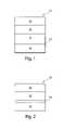
- FIG. 1illustrates a gallium nitride material-based semiconductor structure including a strain-absorbing layer according to one embodiment of the present invention.
- FIG. 2illustrates a gallium nitride material-based semiconductor structure including a strain-absorbing layer according to another embodiment of the present invention.
- FIG. 3illustrates a gallium nitride material-based semiconductor structure including a strain-absorbing layer formed between layers within the structure according to another embodiment of the present invention.
- FIG. 4schematically illustrates a FET device including a strain-absorbing layer according to another embodiment of the invention.
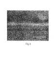
- FIG. 5is a copy of a STEM (scanning transmission electron microscope) image that illustrates the presence of a silicon nitride strain-absorbing layer between an aluminum nitride layer and a silicon substrate as described in Example 1.
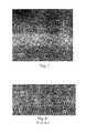
- FIGS. 6 and 7are copies of high-resolution TEM images that illustrates the presence of a silicon nitride strain-absorbing layer between an aluminum nitride layer and a silicon substrate as described in Example 1.
- FIG. 8is a copy of an image published in R. Liu, et. al., Applied Phys. Lett. 83(5), 860 (2003) that illustrates an aluminum nitride layer and silicon substrate interface without the presence of a silicon nitride strain-absorbing layer as described in the Comparative Example.
- the inventionprovides semiconductor structures including a gallium nitride material region and methods associated with such structures.
- the semiconductor structurescan include a strain-absorbing layer formed within the structure.
- the strain-absorbing layermay be formed between the substrate (e.g., a silicon substrate) and an overlying layer, or between layers within the structure. As described further below, it may be preferable for the strain-absorbing layer to be very thin, have an amorphous structure and be formed of a silicon nitride-based material.
- the strain-absorbing layermay reduce the number of misfit dislocations formed in the overlying layer (e.g., a nitride-based material layer) which may limit formation of other types of defects in other overlying layers (e.g., gallium nitride material region), amongst other advantages.
- the presence of the strain-absorbing layermay improve the quality of the gallium nitride material region which can lead to improved device performance.
- FIG. 1illustrates a semiconductor structure 10 according to one embodiment of the invention.
- the semiconductor structureincludes a strain-absorbing layer 12 formed between a substrate 14 and an overlying layer 15 .
- the structureincludes a transition layer 16 formed on the overlying layer and a gallium nitride material region 18 formed on the transition layer.
- the composition, thickness and crystal structure of the strain-absorbing layermay contribute to reducing the number of misfit dislocations in the overlying layer which may decrease defect formation in the gallium nitride material region. This increases the quality of the gallium nitride material region and improves device performance.
- Semiconductor structures of the inventionmay form the basis of a number of semiconductor devices including transistors (e.g., FET), Schottky diodes, light emitting diodes and laser diodes, amongst others.
- a layerWhen a layer is referred to as being “on” or “over” another layer or substrate, it can be directly on the layer or substrate, or an intervening layer also may be present. A layer that is “directly on” another layer or substrate means that no intervening layer is present. It should also be understood that when a layer is referred to as being “on” or “over” another layer or substrate, it may cover the entire layer or substrate, or a portion of the layer or substrate.
- the strain-absorbing layerhelps absorb strain that arises due to lattice differences between the crystal structure of the substrate and the crystal structure of overlying layer 15 (e.g., when overlying layer 15 is formed of an aluminum nitride-based or gallium nitride material). In the absence of the strain-absorbing layer, this strain is typically accommodated by the generation of misfit dislocations in overlying layer 15 at the interface with the substrate. Thus, by providing an alternative mechanism for accommodating stress, the presence of the strain-absorbing layer may reduce the generation of misfit dislocations.
- the strain-absorbing layercan help absorb strain that arises due to differences in the thermal expansion rate of the substrate as compared to the thermal expansion rate of the overlying layer and/or the gallium nitride material region. Such differences can lead to formation of misfit dislocations at the overlying layer/substrate interface, or cracking in either the overlying layer and/or gallium nitride material region. As described further below, transition layer 16 also helps absorb this thermally-induced strain.
- strain-absorbing layer 12is formed of a silicon nitride-based material.
- Silicon nitride-based materialsinclude any silicon nitride-based compound (e.g., Si x N y , such as SiN and Si 3 N 4 , SiCN, amongst others) including non-stoichiometric silicon nitride-based compounds.
- a SiN strain-absorbing layermay be preferred. Silicon nitride material-based strain-absorbing layers may be particularly preferred when formed directly on a silicon substrate, as described further below.
- strain-absorbing layermay be formed of other types of materials according to other embodiments of the invention. Though all of the advantages associated with silicon nitride-based materials may not be achieved in these embodiments.
- the strain-absorbing layerit is preferable for the strain-absorbing layer to have an amorphous (i.e., non-crystalline) crystal structure.
- Amorphous strain-absorbing layersare particularly effective in accommodating strain and, thus, reducing the generation of misfit dislocations.
- the strain-absorbing layermay have a single crystal or poly-crystalline structure. In these cases, however, all of the advantages associated with the amorphous layer may not be realized.
- the strain-absorbing layerit is preferred for the strain-absorbing layer to be very thin, particularly when formed of amorphous and/or silicon nitride-based materials. It has been discovered that very thin strain-absorbing layers (e.g., silicon nitride-based strain-absorbing layers) may enable formation of overlying layer(s) having an epitaxial relationship with the substrate, while also being effective in reducing the number of misfit dislocations. In certain cases (e.g., when the strain-absorbing layer is amorphous), it is desirable for the strain-absorbing layer to have a thickness that is large enough to accommodate sufficient strain associated with lattice and thermal expansion differences between the substrate and overlying layer 15 to reduce generation of misfit dislocations.
- very thin strain-absorbing layerse.g., silicon nitride-based strain-absorbing layers
- the strain-absorbing layermay also be desirable for the strain-absorbing layer to be thin enough so that the overlying layer has an epitaxial relationship with the substrate. This can be advantageous for formation of a high quality, single crystal gallium nitride material region. If the strain-absorbing layer is too thick, then the overlying layer is not formed with epitaxial relationship with the substrate.
- the strain-absorbing layerhas a thickness of less than about 100 Angstroms which, in these embodiments, can allow the epitaxial relationship between the substrate and the overlying layer. In some embodiments, it may be preferable for the strain-absorbing layer to have a thickness of less than about 50 Angstroms to allow for the epitaxial relationship.
- the strain-absorbing layermay have a thickness of greater than about 10 Angstroms which, in these embodiments, is sufficient to accommodate strain (e.g., resulting from lattice and thermal expansion differences) and can facilitate forming a strain-absorbing layer that covers the entire substrate, as described further below. In other embodiments, the strain-absorbing layer may have a thickness of greater than about 20 Angstroms to sufficiently accommodate strain.
- Suitable thickness ranges for the strain-absorbing layerinclude all of those defined by the ranges described above (e.g., greater than about 10 Angstroms and less than about 100 Angstroms, greater than about 10 Angstroms and less than about 50 Angstroms, and the like). Also, the strain-absorbing layer thickness may be between about 20 Angstroms and about 70 Angstroms.
- suitable thicknesses of the strain-absorbing layermay depend on a number of factors including the composition and crystal structure of the strain-absorbing layer; the composition, thickness and crystal structure of the overlying layer; as well as the composition, thickness, and crystal structure of the substrate, amongst other factors. Suitable thicknesses may be determined by measuring the effect of thickness on misfit dislocation density and other factors (e.g., the ability to deposit an overlying layer having an epitaxial relationship with the substrate, etc.). It is also possible for the strain-absorbing layer to have a thickness outside the above ranges.
- the thickness of the strain-absorbing layeris relatively uniform across the entire layer.
- the strain-absorbing layermay have a thickness uniformity variation of less than 25 percent, or less than 10 percent, across the entire strain-absorbing layer.
- the strain-absorbing layermay be formed by nitridating a top surface region of a silicon substrate. That is, the surface region of the substrate may be converted from silicon to a silicon nitride-based material to form the strain-absorbing layer.
- such strain-absorbing layersmay be referred to as being “formed on the substrate”, “formed over the substrate”, “formed directly on the substrate” and as “covering the substrate”.
- Such phrasesalso refer to strain-absorbing layers that are formed by depositing a separate layer (e.g., using a separate nitrogen source and silicon source) on the top surface of the substrate and are not formed by converting a surface region of the substrate.
- the strain-absorbing layercovers substantially the entire top surface of the substrate. This arrangement may be preferable to minimize the number of misfit dislocations in the overlying layer. In other embodiments, the strain-absorbing layer may cover a majority of the top surface of the substrate (e.g., greater than 50 percent or greater than 75 percent of the top surface area).
- strain-absorbing layer 12is formed across the entire area between the substrate and the overlying layer. That is, the strain-absorbing layer separates the substrate and the overlying layer at all points with the strain-absorbing layer being directly on the substrate and the overlying layer being directly on the strain-absorbing layer. This arrangement may be preferable to minimize the number of misfit dislocations in the overlying layer.
- the strain-absorbing layermay be formed across a majority of the area (e.g., greater than 50 percent, or greater than 75 percent) between the substrate and the overlying layer. If the strain-absorbing layer is not present across the entire (or, at least, the majority of the) area between the substrate and the overlying layer, the above-noted advantages associated with the strain-absorbing layer may not be realized.
- strain-absorbing layercovers the substrate (and the area between the overlying layer and the substrate) in the present invention may be distinguished from certain prior art techniques in which a discontinuous silicon nitride layer is formed (in some cases, inadvertently) between a silicon substrate and an overlying layer.
- the strain-absorbing layermay be positioned in other locations such as between two different layers (e.g., the embodiment of FIG. 3 ). In these embodiments, the strain-absorbing layer may reduce the formation of misfit dislocations in the layer that overlies the strain-absorbing layer.
- the presence of the strain-absorbing layeradvantageously results in very low misfit dislocation densities within the overlying layer (e.g., at, or very near, an interface between the strain-absorbing layer and the overlying layer).
- Misfit dislocationstypically are formed at (or, very near) the interface between two materials as a result of incoherency due to differences in atomic structures of the materials.
- the misfit dislocation density in the overlying layeris less than about 10 10 defects/cm 2 ; and, in other embodiments, less than about 10 8 defects/cm 2 . Even lower misfit dislocation densities in the overlying layer may be achieved, for example, less than about 10 5 defects/cm 2 . In some cases, the presence of misfit dislocations may not be readily detectable which generally means that the misfit dislocation density is less than about 10 2 defects/cm 2 .
- the specific misfit dislocation densitydepends, in part, on the particular structure including factors such as the thickness, composition and crystal structure of the strain-absorbing layer; the composition, thickness and crystal structure of the overlying layer; as well as the composition, thickness, and crystal structure of the substrate, amongst other factors.
- misfit dislocation density rangesmay be found in the overlying layer at, or very near (e.g., 20 nm), the interface with the strain-absorbing layer; and, also may be found at other regions within the overlying layer.
- Misfit dislocation densitymay be measured using known techniques.
- the techniquesgenerally involve inspection of the atomic structure of a sample (e.g., an interface) using high magnification to determine the presence of misfit dislocations over a representative area.
- high resolution transmission electron microscopyTEM
- One suitable techniqueinvolves counting the number of dislocations over a representative area using high resolution-TEM images.
- the misfit dislocation densityis calculated by dividing the number of dislocations by the area.
- the misfit dislocation densityis expressed in units of defects/cm 2 .
- the overlying layermay have misfit dislocation densities greater than the above-noted ranges.
- the very low misfit dislocation densities achievable in the overlying layer in structures of the present inventionmay lead to a number of advantages including reducing defects in the gallium nitride material region, as described further below.
- structure 10may include an overlying layer 15 formed of a nitride-based material.
- Suitable nitride-based materialsinclude, but are not limited to, aluminum nitride-based materials (e.g., aluminum nitride, aluminum nitride alloys) and gallium nitride based-materials (e.g., gallium nitride, gallium nitride alloys).
- the overlying layerhas a constant composition.
- the overlying layermay be compositionally-graded. Suitable compositionally-graded layers are described further below and have been described in commonly-owned U.S. Pat. No. 6,649,287, entitled “Gallium Nitride Materials and Methods” filed on Dec. 14, 2000, which is incorporated herein by reference.
- the overlying layermay have a single crystal structure.
- the thickness of the strain-absorbing layeris controlled so that the overlying layer has an epitaxial relationship with the substrate. It may be advantageous for the overlying layer to have a single crystal structure because it facilitates formation of a single crystal, high quality gallium nitride material region. In some embodiments, the overlying layer has a different crystal structure than the substrate. It should also be understood that the overlying layer may not have a single crystal structure and may be amorphous or polycrystalline, though all of the advantages associated with the single crystal overlying layers may not be achieved.
- the overlying layermay have any suitable thickness.
- the overlying layermay be between about 10 nanometers and 5 microns, though other thicknesses are also possible.
- transition layer 16is formed directly on the overlying layer.
- the transition layermay be formed of a compositionally-graded material (e.g., a compositionally-graded nitride-based material). Suitable compositionally-graded layers have been described in commonly-owned U.S. Pat. No. 6,649,287 which is incorporated by reference above. Compositionally-graded transition layers have a composition that is varied across at least a portion of the layer.
- Compositionally-graded transition layersare particularly effective in reducing crack formation in gallium nitride material regions formed on the transition layer by lowering thermal stresses that result from differences in thermal expansion rates between the gallium nitride material and the substrate (e.g., silicon).
- the transition layeris compositionally-graded and formed of an alloy of gallium nitride such as Al x In y Ga (1-x-y) N, Al x Ga (1-x) N, and In y Ga (1-y) N.
- the concentration of at least one of the elements (e.g., Ga, Al, In) of the alloyis varied across at least a portion of the thickness of the transition layer.
- transition layer 16has an Al x In y Ga (1-x-y) N composition
- x and/or ymay be varied.
- the transition layerhas a Al x Ga (1-x) N composition
- xmay be varied.
- ymay be varied.
- the transition layermay have a low gallium concentration at a back surface which is graded to a high gallium concentration at a front surface. It has been found that such transition layers are particularly effective in relieving internal stresses within gallium nitride material region 18 .
- the transition layermay have a composition of Al x Ga (1-x) N, where x is decreased from the back surface to the front surface of the transition layer (e.g., x is decreased from a value of 1 at the back surface of the transition layer to a value of 0 at the front surface of the transition layer).
- structure 10includes an aluminum nitride overlying layer 15 and a compositionally-graded transition layer 16 .
- the compositionally-graded transition layermay have a composition of Al x Ga (1-x) N, where x is graded from a value of 1 at the back surface of the transition layer to a value of 0 at the front surface of the transition layer.
- the composition of the transition layermay be graded discontinuously (e.g., step-wise) or continuously.
- One discontinuous grademay include steps of AlN, Al 0.6 Ga 0.4 N and Al 0.3 Ga 0.7 N proceeding in a direction toward the gallium nitride material region.
- transition layer 16may have a constant composition and may not be compositionally-graded (e.g., when the overlying layer is compositionally-graded). It should also be understood that in some embodiments of the invention, as shown in FIG. 2 , a separate transition layer is not present between the overlying layer and the gallium nitride material region.
- structure 20includes overlying layer 15 formed directly on top of strain-absorbing layer 12 and gallium nitride material region 18 formed directly on the overlying layer. In this embodiment, it may be preferable for the overlying layer to be compositionally-graded as described above.
- the overlying layer and/or transition layerare typically (though not always) not part of the active region of the device.
- the overlying layer and/or transition layermay be formed to facilitate deposition of gallium nitride material region 18 .
- the overlying layer and/or transition layermay have other functions including functioning as a heat spreading layer that helps remove heat from active regions of the semiconductor structure during operation of a device.
- such transition layers that function as heat spreading layershave been described in commonly-owned, co-pending U.S. patent application Ser. No. 09/792,409 entitled “Gallium Nitride Materials Including Thermally-Conductive Regions,” filed Feb. 23, 2001, which is incorporated herein by reference.
- Gallium nitride material region 18comprises at least one gallium nitride material layer.
- gallium nitride materialrefers to gallium nitride (GaN) and any of its alloys, such as aluminum gallium nitride (Al x Ga (1-x) N), indium gallium nitride (In y Ga (1-y) N), aluminum indium gallium nitride (Al x In y Ga (1-x-y) N), gallium arsenide phosporide nitride (GaAs a P b N (1-a-b) ), aluminum indium gallium arsenide phosporide nitride (Al x In y Ga (1-x-y) As a P b N (1-a-b) ), amongst others.
- Gallium nitride materialsmay be doped n-type or p-type, or may be intrinsic. Suitable gallium nitride materials have been described in U.S. Pat. No. 6,649,287, incorporated by reference above.
- gallium nitride material region 18includes only one gallium nitride material layer. In other cases, gallium nitride material region 18 includes more than one gallium nitride material layer.
- the gallium nitride material regionmay include multiple layers (e.g., 18 a , 18 b , 18 c ) as shown in FIG. 4 .
- the value of x in the gallium nitride material of layer 18 bmay have a value that is between 0.05 and 1.0 greater than the value of x in the gallium nitride material of layer 18 a , or between 0.05 and 0.5 greater than the value of x in the gallium nitride material of layer 18 a .
- layer 18 bmay be formed of Al 0.26 Ga 0.74 N, while layer 18 a is formed of GaN. This difference in aluminum concentration may lead to formation of a highly conductive region at the interface of the layers 18 b , 18 a (i.e., a 2-D electron gas region).
- layer 18 cmay be formed of GaN.
- Gallium nitride material region 18also may include one or more layers that do not have a gallium nitride material composition such as other III-V compounds or alloys, oxide layers, and metallic layers.
- Gallium nitride material region 18is of high enough quality so as to permit the formation of devices therein.
- the presence of the strain-absorbing layermay reduce the misfit dislocation density in the overlying layer which can reduce formation of defects in the gallium nitride material region. For example, the generation of point defects, line defects, and planar defects may be reduced. By limiting defect generation in the gallium nitride material region, device performance can be improved.
- the low misfit dislocation densitiescan also limit creation of electronic states within energy bands of the gallium nitride material regions which also negatively effect device performance.
- gallium nitride material region 18also has a low crack level.
- the transition layer (particularly when compositionally-graded) and/or overlying layermay reduce crack formation.
- Gallium nitride materials having low crack levelshave been described in U.S. Pat. No. 6,649,287 incorporated by reference above.
- the gallium nitride material regionhas a crack level of less than 0.005 ⁇ m/ ⁇ m 2 .
- the gallium nitride material regionhas a very low crack level of less than 0.001 ⁇ m/ ⁇ m 2 .
- gallium nitride material region 18includes a layer (or layers) which have a single crystal (i.e., monocrystalline) structure. In some cases, the gallium nitride material region includes one or more layers having a Wurtzite (hexagonal) structure.
- the thickness of gallium nitride material region 18 and the number of different layersare dictated, at least in part, by the requirements of the specific device. At a minimum, the thickness of the gallium nitride material region is sufficient to permit formation of the desired structure or device.
- the gallium nitride material regiongenerally has a thickness of greater than 0.1 micron, though not always. In other cases, gallium nitride material region 18 has a thickness of greater than 0.5 micron, greater than 2.0 microns, or even greater than 5.0 microns.
- substrate 14is a silicon substrate.
- a silicon substraterefers to any substrate that includes a silicon surface.
- suitable silicon substratesinclude substrates that are composed entirely of silicon (e.g., bulk silicon wafers), silicon-on-insulator (SOI) substrates, silicon-on-sapphire substrate (SOS), and SIMOX substrates, amongst others.
- Suitable silicon substratesalso include substrates that have a silicon wafer bonded to another material such as diamond, AlN, or other polycrystalline materials. Silicon substrates having different crystallographic orientations may be used, though single crystal silicon substrates are preferred. In some cases, silicon ( 111 ) substrates are preferred. In other cases, silicon ( 100 ) substrates are preferred.
- substratesmay also be used including sapphire, silicon carbide, indium phosphide, silicon germanium, gallium arsenide, gallium nitride, aluminum nitride, or other III-V compound substrates.
- silicon substratesin embodiments that do not use silicon substrates, all of the advantages associated with silicon substrates may not be achieved.
- non-nitride material-based substratessuch as silicon, sapphire, silicon carbide, indium phosphide, silicon germanium and gallium arsenide.
- Substrate 14may have any suitable dimensions and its particular dimensions are dictated by the application. Suitable diameters include, but are not limited to, about 2 inches (50 mm), 4 inches (100 mm), 6 inches (150 mm), and 8 inches (200 mm).
- the strain-absorbing layermay be used to form a high quality gallium nitride material region on substrates (e.g., silicon substrates) over a variety of thicknesses. In some cases, it may be preferable for the substrate to be relatively thick, such as greater than about 125 micron (e.g., between about 125 micron and about 800 micron, or between about 400 micron and 800 micron).
- Relatively thick substratesmay be easy to obtain, process, and can resist bending which can occur, in some cases, in thinner substrates.
- thinner substratese.g., less than 125 microns
- the substrateinitially is relatively thick (e.g., between about 200 microns and 800 microns) and then is thinned during a later processing step (e.g., to less than 150 microns).
- the substrateis substantially planar in the final device or structure.
- Substantially planar substratesmay be distinguished from substrates that are textured and/or have trenches formed therein (e.g., as in U.S. Pat. No. 6,265,289).
- the layers/regions of the devicee.g., strain-absorbing layer, overlying layer, transition layer, gallium nitride material region
- such layers/regionsmay be grown in vertical (e.g., non-lateral) growth processes.
- Planar substrates and layers/regionscan be advantageous in some embodiments, for example, to simplify processing. Though it should be understood that, in some embodiments of the invention, lateral growth processes may be used as described further below.
- FIG. 3illustrates a semiconductor structure 22 according to another embodiment of the invention.
- strain-absorbing layer 12is formed between layers within the structure, and is not formed directly on the substrate.
- the strain-absorbing layermay be formed between an underlying layer 24 and an overlying layer 15 .
- the strain-absorbing layermay reduce the formation of misfit dislocations in overlying layer 15 as described above in connection with the embodiments of FIG. 1 .
- Underlying layer 24may be formed of a variety of semiconductor materials.
- the underlying layeris formed of a nitride-based material. Suitable nitride-based materials include, but are not limited to, aluminum nitride-based materials (e.g., aluminum nitride, aluminum nitride alloys) and gallium nitride materials. In some embodiments, it may be preferred for the underlying material to have a different composition than the overlying material. The underlying layer may also have a different crystal structure than the overlying layer.
- the underlying materialmay be formed of non-nitride based materials.
- the semiconductor structures illustrated in FIGS. 1-3may form the basis of a variety of semiconductor devices. Suitable devices include, but are not limited to, transistors (e.g., FETs) as well as light-emitting devices including LEDs and laser diodes. The devices have active regions that are typically, at least in part, within the gallium nitride material region. Also, the devices include a variety of other functional layers and/or features (e.g., electrodes).
- FIG. 4schematically illustrates a FET device 30 according to one embodiment of the invention which is similar to a FET device described in U.S. patent application Ser. No. 10/740,376 except device 30 includes strain-absorbing layer 12 .
- Device 30includes a source electrode 34 , a drain electrode 36 and a gate electrode 38 formed on gallium nitride material region 18 (which includes a first layer 18 b and a second layer 18 a ).
- the devicealso includes an electrode defining layer 40 which, as shown, is a passivating layer that protects and passivates the surface of the gallium nitride material region.
- a via 42is formed within the electrode defining layer in which the gate electrode is, in part, formed.
- Strain-absorbing layer 12is formed directly on the substrate and overlying layer 15 is formed directly on the strain-absorbing layer.
- the overlying layeris compositionally-graded.
- the overlying layermay have a constant composition (e.g., aluminum nitride or an aluminum nitride alloy) and a compositionally-graded transition layer is formed on the strain-absorbing layer.
- strain-absorbing layermay also be included in structures and devices described in U.S. Pat. No. 6,649,287 which is incorporated herein by reference above.
- strain-absorbing layermay also be included in structures and devices described in commonly-owned U.S. Pat. No. 6,611,002 entitled “Gallium Nitride Material Devices and Methods Including Backside Vias” which is incorporated herein by reference.
- strain-absorbing layermay be within the scope of the present invention including structures and devices that are not specifically described herein.
- Other structuresmay include other layers and/or features, amongst other differences.
- the strain-absorbing layeris a silicon nitride-based material (e.g., amorphous SiN)
- the strain-absorbing layermay be formed by nitridating a top surface of the silicon substrate as noted above.
- nitrogenreacts with a top surface region of the silicon substrate to form a silicon nitride-based layer.
- the top surfacemay be nitridated by exposing the silicon substrate to a gaseous source of nitrogen at elevated temperatures.
- ammoniamay be introduced into a reaction chamber in which a silicon substrate is positioned.
- the temperature in the reaction chambermay be between about 1000° C. and about 1100° C. and the pressure may be between about 20 torr and about 40 torr (in some cases, about 30 torr).
- the reaction between nitrogen and the silicon substrateis allowed to proceed for a reaction time selected to produce a layer having a desired thickness.
- the strain-absorbing layermay be formed in-situ with the overlying layer (and, in some cases, subsequent layers) of the structure. That is, the strain-absorbing layer may be formed during the same deposition step as the overlying layer (and, in some cases, subsequent layers).
- a nitrogen sourcee.g., ammonia
- a second source gasmay be introduced into the chamber after a selected time delay after the nitrogen source. The second source reacts with the nitrogen source to form the overlying layer, thus, ending growth of the strain-absorbing layer.
- an aluminum sourcee.g., trimethylaluminum
- the nitrogen sourcee.g., ammonia
- the time delayis selected so that the strain-absorbing layer grows to a desired thickness.
- the reaction between the second source (e.g., aluminum source) and the nitrogen sourceis allowed to proceed for a sufficient time to produce the overlying layer.
- the reaction conditionsare selected appropriately.
- the reaction temperaturemay be greater than 700° C., such as between about 1000° C. and about 1100° C. In some cases, lower growth temperatures may be used including temperatures between about 500° C. and about 600° C.
- the strain-absorbing layermay be formed in a separate process than the overlying layer and subsequent layers.
- the strain-absorbing layermay be formed on the substrate in a first process. Then, at a later time, the overlying layers may be formed on the strain-absorbing layer in a second process.
- the overlying layeris grown in a vertical growth process. That is, the overlying layer is grown in a vertical direction with respect to the strain-absorbing layer.
- the ability to vertically grow the strain-absorbing layer having low misfit dislocation densitiesmay be advantageous as compared to lateral growth processes which may be more complicated.
- Transition layer 16 and gallium nitride material region 18may also be grown in the same deposition step as the overlying layer and the strain-absorbing layer. In such processes, suitable sources are introduced into the reaction chamber at appropriate times. Suitable MOCVD processes to form compositionally-graded transition layers and gallium nitride material region over a silicon substrate have been described in U.S. Pat. No. 6,649,287 incorporated by reference above.
- gallium nitride material region 18has different layers, in some cases, it is preferable to use a single deposition step to form the entire region 18 .
- the processing parametersmay be suitably changed at the appropriate time to form the different layers.
- the transition layer and the gallium nitride material regionmay be grown separately from the strain-absorbing layer and overlying layer.
- the gallium nitride material region and transition layermay be grown in a vertical growth process. That is, these regions are grown in a vertical direction with respect to underlying layers.
- the ability to vertically grow the gallium nitride material region having low misfit dislocation densitiesmay be advantageous as compared to lateral growth processes which may be more complicated.
- gallium nitride material region 18it is possible to grow, at least a portion of, gallium nitride material region 18 using a lateral epitaxial overgrowth (LEO) technique that involves growing an underlying gallium nitride layer through mask openings and then laterally over the mask to form the gallium nitride material region, for example, as described in U.S. Pat. No. 6,051,849.
- LEOlateral epitaxial overgrowth
- gallium nitride material region 18it is possible to grow the gallium nitride material region 18 using a pendeoepitaxial technique that involves growing sidewalls of gallium nitride material posts into trenches until growth from adjacent sidewalls coalesces to form a gallium nitride material region, for example, as described in U.S. Pat. No. 6,265,289.
- gallium nitride material regions with very low defect densitiesare achievable.
- at least a portion of the gallium nitride material regionmay have a defect density of less than about 10 5 defects/cm 2 .
- This exampleillustrates the formation of a silicon nitride-based material strain-absorbing layer on a silicon substrate according to one embodiment of the present invention.
- a 100 mm silicon substratewas placed in a reaction chamber. Ammonia gas was introduced into the chamber as a nitrogen source. The temperature was maintained at 1030° C. and the pressure at about 30 torr. A layer of amorphous silicon nitride (SiN) was formed.
- SiNamorphous silicon nitride
- TMAwas introduced into the chamber as an aluminum source.
- the temperature and pressurewere respectively maintained at 1030° C. and about 30 torr. Growth proceeded for 30 minutes.
- FIGS. 5-7are copies of micrograph images that illustrate the resulting structure.
- FIG. 5is a copy of a STEM (scanning transmission electron microscope) image.
- FIGS. 6 and 7are copies of high-resolution TEM images. The images show the presence of an amorphous silicon nitride strain-absorbing layer formed between a single crystal aluminum nitride layer and a single crystal silicon substrate.
- the high-resolution TEM imagesshow the crystal structures of the resulting layers and substrate.
- the imagesshow that the crystal structure of the silicon nitride layer is amorphous, the crystal structure of the silicon substrate is cubic and the crystal structure of the aluminum nitride is hexagonal.
- the aluminum nitride layerhas an epitaxial relationship with the substrate.
- the imagesalso show the absence of misfit dislocations at (or near) the interface of the amorphous silicon nitride strain-absorbing layer and the aluminum nitride layer.
- strain-absorbing layers of the present inventionmay be used to limit misfit dislocation density.
- This exampleillustrates the presence of misfit dislocations in an aluminum nitride layer formed directly on a silicon substrate in the absence of a strain-absorbing layer of the present invention.
- FIG. 8is a copy of an image published in R. Liu, et. al., Applied Phys. Lett. 83(5), 860 (2003).
- the imageillustrates an aluminum nitride layer formed directly on a silicon substrate, without the presence of a silicon nitride strain-absorbing layer, following procedures described in the article. Misfit dislocations are indicated by “ ”.
- the interface coherenceis indicated by solid lines that connect ⁇ 111 ⁇ Si and ⁇ 1-100 ⁇ AlN lattice planes.
Landscapes
- Engineering & Computer Science (AREA)
- Microelectronics & Electronic Packaging (AREA)
- Condensed Matter Physics & Semiconductors (AREA)
- General Physics & Mathematics (AREA)
- Manufacturing & Machinery (AREA)
- Computer Hardware Design (AREA)
- Physics & Mathematics (AREA)
- Power Engineering (AREA)
- Chemical & Material Sciences (AREA)
- Materials Engineering (AREA)
- Crystallography & Structural Chemistry (AREA)
- Recrystallisation Techniques (AREA)
- Led Devices (AREA)
- Semiconductor Lasers (AREA)
Abstract
Description

Claims (29)
Priority Applications (8)
| Application Number | Priority Date | Filing Date | Title |
|---|---|---|---|
| US10/879,703US7339205B2 (en) | 2004-06-28 | 2004-06-28 | Gallium nitride materials and methods associated with the same |
| US11/096,505US7352015B2 (en) | 2004-06-28 | 2005-04-01 | Gallium nitride materials and methods associated with the same |
| JP2007519306AJP2008504715A (en) | 2004-06-28 | 2005-06-24 | Gallium nitride materials and methods |
| PCT/US2005/022488WO2006012298A1 (en) | 2004-06-28 | 2005-06-24 | Gallium nitride material and methods associated with the same |
| EP15154901.1AEP2894662A1 (en) | 2004-06-28 | 2005-06-24 | Semiconductor structure including a gallium nitride layer on a substrate with an intermediate layer of amorphous silicon nitride |
| EP05763560AEP1769529A1 (en) | 2004-06-28 | 2005-06-24 | Gallium nitride materials and methods associated with the same |
| US12/023,451US8748298B2 (en) | 2004-06-28 | 2008-01-31 | Gallium nitride materials and methods associated with the same |
| US12/023,480US10096701B2 (en) | 2004-06-28 | 2008-01-31 | Gallium nitride materials and methods associated with the same |
Applications Claiming Priority (1)
| Application Number | Priority Date | Filing Date | Title |
|---|---|---|---|
| US10/879,703US7339205B2 (en) | 2004-06-28 | 2004-06-28 | Gallium nitride materials and methods associated with the same |
Related Child Applications (2)
| Application Number | Title | Priority Date | Filing Date |
|---|---|---|---|
| US11/096,505Continuation-In-PartUS7352015B2 (en) | 2004-06-28 | 2005-04-01 | Gallium nitride materials and methods associated with the same |
| US12/023,480DivisionUS10096701B2 (en) | 2004-06-28 | 2008-01-31 | Gallium nitride materials and methods associated with the same |
Publications (2)
| Publication Number | Publication Date |
|---|---|
| US20050285141A1 US20050285141A1 (en) | 2005-12-29 |
| US7339205B2true US7339205B2 (en) | 2008-03-04 |
Family
ID=35033763
Family Applications (4)
| Application Number | Title | Priority Date | Filing Date |
|---|---|---|---|
| US10/879,703Expired - LifetimeUS7339205B2 (en) | 2004-06-28 | 2004-06-28 | Gallium nitride materials and methods associated with the same |
| US11/096,505Expired - LifetimeUS7352015B2 (en) | 2004-06-28 | 2005-04-01 | Gallium nitride materials and methods associated with the same |
| US12/023,451Expired - LifetimeUS8748298B2 (en) | 2004-06-28 | 2008-01-31 | Gallium nitride materials and methods associated with the same |
| US12/023,480Active2031-05-24US10096701B2 (en) | 2004-06-28 | 2008-01-31 | Gallium nitride materials and methods associated with the same |
Family Applications After (3)
| Application Number | Title | Priority Date | Filing Date |
|---|---|---|---|
| US11/096,505Expired - LifetimeUS7352015B2 (en) | 2004-06-28 | 2005-04-01 | Gallium nitride materials and methods associated with the same |
| US12/023,451Expired - LifetimeUS8748298B2 (en) | 2004-06-28 | 2008-01-31 | Gallium nitride materials and methods associated with the same |
| US12/023,480Active2031-05-24US10096701B2 (en) | 2004-06-28 | 2008-01-31 | Gallium nitride materials and methods associated with the same |
Country Status (4)
| Country | Link |
|---|---|
| US (4) | US7339205B2 (en) |
| EP (2) | EP2894662A1 (en) |
| JP (1) | JP2008504715A (en) |
| WO (1) | WO2006012298A1 (en) |
Cited By (27)
| Publication number | Priority date | Publication date | Assignee | Title |
|---|---|---|---|---|
| US20070108466A1 (en)* | 2005-08-31 | 2007-05-17 | University Of Florida Research Foundation, Inc. | Group III-nitrides on Si substrates using a nanostructured interlayer |
| US20070272957A1 (en)* | 2005-12-02 | 2007-11-29 | Nitronex Corporation | Gallium nitride material devices and associated methods |
| US20080054248A1 (en)* | 2006-09-06 | 2008-03-06 | Chua Christopher L | Variable period variable composition supperlattice and devices including same |
| US20080200013A1 (en)* | 2004-06-28 | 2008-08-21 | Nitronex Corporation | Gallium nitride materials and methods associated with the same |
| US20080217647A1 (en)* | 2007-03-06 | 2008-09-11 | Seoul Opto Device Co., Ltd. | Method of forming nitride semiconductor layer on patterned substrate and light emitting diode having the same |
| US7791106B2 (en) | 2005-05-03 | 2010-09-07 | Nitronex Corporation | Gallium nitride material structures including substrates and methods associated with the same |
| EP2518880A2 (en) | 2011-04-28 | 2012-10-31 | International Rectifier Corporation | Integrated power stage |
| EP2521176A1 (en) | 2011-05-04 | 2012-11-07 | International Rectifier Corporation | High voltage cascoded III-nitride rectifier package comprising conductive clips between electrodes of components and the surface of a package support member |
| EP2521171A1 (en) | 2011-05-04 | 2012-11-07 | International Rectifier Corporation | High voltage cascoded III-nitride rectifier package with stamped leadframe |
| EP2521172A1 (en) | 2011-05-04 | 2012-11-07 | International Rectifier Corporation | High voltage cascoded III-nitride rectifier package with etched leadframe |
| WO2013001014A1 (en) | 2011-06-30 | 2013-01-03 | Soitec | Method for manufacturing a thick epitaxial layer of gallium nitride on a silicon or similar substrate and layer obtained using said method |
| EP2546880A2 (en) | 2011-07-15 | 2013-01-16 | International Rectifier Corporation | Composite semiconductor device with integrated diode |
| EP2546883A2 (en) | 2011-07-15 | 2013-01-16 | International Rectifier Corporation | Composite Semiconductor Device with a SOI Substrate Having an Integrated Diode |
| US8513643B2 (en) | 2006-09-06 | 2013-08-20 | Palo Alto Research Center Incorporated | Mixed alloy defect redirection region and devices including same |
| US8664679B2 (en) | 2011-09-29 | 2014-03-04 | Toshiba Techno Center Inc. | Light emitting devices having light coupling layers with recessed electrodes |
| EP2706651A2 (en) | 2012-09-07 | 2014-03-12 | International Rectifier Corporation | Integrated power stage with group III-V transistors |
| US8698163B2 (en) | 2011-09-29 | 2014-04-15 | Toshiba Techno Center Inc. | P-type doping layers for use with light emitting devices |
| US8853668B2 (en) | 2011-09-29 | 2014-10-07 | Kabushiki Kaisha Toshiba | Light emitting regions for use with light emitting devices |
| US8952419B2 (en) | 2010-09-28 | 2015-02-10 | Samsung Electronics Co., Ltd. | Semiconductor devices and methods of manufacturing the same |
| US8957454B2 (en) | 2011-03-03 | 2015-02-17 | International Rectifier Corporation | III-Nitride semiconductor structures with strain absorbing interlayer transition modules |
| US9012921B2 (en) | 2011-09-29 | 2015-04-21 | Kabushiki Kaisha Toshiba | Light emitting devices having light coupling layers |
| EP2869347A1 (en) | 2013-10-30 | 2015-05-06 | International Rectifier Corporation | Group III-V device including a buffer termination body |
| EP2879184A1 (en) | 2013-12-02 | 2015-06-03 | International Rectifier Corporation | Group III-V transistor with semiconductor field plate |
| EP2881992A1 (en) | 2013-12-06 | 2015-06-10 | International Rectifier Corporation | Dual-gated group III-V merged transistor |
| US9130068B2 (en) | 2011-09-29 | 2015-09-08 | Manutius Ip, Inc. | Light emitting devices having dislocation density maintaining buffer layers |
| US9178114B2 (en) | 2011-09-29 | 2015-11-03 | Manutius Ip, Inc. | P-type doping layers for use with light emitting devices |
| US10636899B2 (en) | 2016-11-15 | 2020-04-28 | Infineon Technologies Austria Ag | High electron mobility transistor with graded back-barrier region |
Families Citing this family (43)
| Publication number | Priority date | Publication date | Assignee | Title |
|---|---|---|---|---|
| US7638346B2 (en)* | 2001-12-24 | 2009-12-29 | Crystal Is, Inc. | Nitride semiconductor heterostructures and related methods |
| US8545629B2 (en)* | 2001-12-24 | 2013-10-01 | Crystal Is, Inc. | Method and apparatus for producing large, single-crystals of aluminum nitride |
| US20060005763A1 (en) | 2001-12-24 | 2006-01-12 | Crystal Is, Inc. | Method and apparatus for producing large, single-crystals of aluminum nitride |
| JP4869564B2 (en)* | 2003-11-28 | 2012-02-08 | 新日本無線株式会社 | Nitride semiconductor device and manufacturing method thereof |
| US7071498B2 (en)* | 2003-12-17 | 2006-07-04 | Nitronex Corporation | Gallium nitride material devices including an electrode-defining layer and methods of forming the same |
| US7687827B2 (en)* | 2004-07-07 | 2010-03-30 | Nitronex Corporation | III-nitride materials including low dislocation densities and methods associated with the same |
| US20060214289A1 (en)* | 2004-10-28 | 2006-09-28 | Nitronex Corporation | Gallium nitride material-based monolithic microwave integrated circuits |
| CN101326642A (en)* | 2005-10-04 | 2008-12-17 | 尼特罗奈克斯公司 | GaN material transistors and methods for broadband applications |
| US8349077B2 (en) | 2005-11-28 | 2013-01-08 | Crystal Is, Inc. | Large aluminum nitride crystals with reduced defects and methods of making them |
| US7566913B2 (en) | 2005-12-02 | 2009-07-28 | Nitronex Corporation | Gallium nitride material devices including conductive regions and methods associated with the same |
| JP5281408B2 (en) | 2005-12-02 | 2013-09-04 | クリスタル・イズ,インコーポレイテッド | Doped aluminum nitride crystal and method for producing the same |
| US9034103B2 (en) | 2006-03-30 | 2015-05-19 | Crystal Is, Inc. | Aluminum nitride bulk crystals having high transparency to ultraviolet light and methods of forming them |
| US8012257B2 (en) | 2006-03-30 | 2011-09-06 | Crystal Is, Inc. | Methods for controllable doping of aluminum nitride bulk crystals |
| EP1883103A3 (en)* | 2006-07-27 | 2008-03-05 | Interuniversitair Microelektronica Centrum | Deposition of group III-nitrides on Ge |
| US20100269819A1 (en)* | 2006-08-14 | 2010-10-28 | Sievers Robert E | Human Powered Dry Powder Inhaler and Dry Powder Inhaler Compositions |
| US9771666B2 (en) | 2007-01-17 | 2017-09-26 | Crystal Is, Inc. | Defect reduction in seeded aluminum nitride crystal growth |
| US8323406B2 (en) | 2007-01-17 | 2012-12-04 | Crystal Is, Inc. | Defect reduction in seeded aluminum nitride crystal growth |
| WO2008094464A2 (en) | 2007-01-26 | 2008-08-07 | Crystal Is, Inc. | Thick pseudomorphic nitride epitaxial layers |
| US8080833B2 (en) | 2007-01-26 | 2011-12-20 | Crystal Is, Inc. | Thick pseudomorphic nitride epitaxial layers |
| US8362503B2 (en) | 2007-03-09 | 2013-01-29 | Cree, Inc. | Thick nitride semiconductor structures with interlayer structures |
| US7825432B2 (en)* | 2007-03-09 | 2010-11-02 | Cree, Inc. | Nitride semiconductor structures with interlayer structures |
| US7795070B2 (en)* | 2007-03-30 | 2010-09-14 | Texas Instruments Incorporated | Semiconductor device including an amorphous nitrided silicon adhesion layer and method of manufacture therefor |
| US8088220B2 (en)* | 2007-05-24 | 2012-01-03 | Crystal Is, Inc. | Deep-eutectic melt growth of nitride crystals |
| US7745848B1 (en) | 2007-08-15 | 2010-06-29 | Nitronex Corporation | Gallium nitride material devices and thermal designs thereof |
| KR100901822B1 (en)* | 2007-09-11 | 2009-06-09 | 주식회사 실트론 | Gallium nitride growth substrate and gallium nitride substrate manufacturing method |
| US8026581B2 (en)* | 2008-02-05 | 2011-09-27 | International Rectifier Corporation | Gallium nitride material devices including diamond regions and methods associated with the same |
| US8343824B2 (en) | 2008-04-29 | 2013-01-01 | International Rectifier Corporation | Gallium nitride material processing and related device structures |
| JP2011023534A (en) | 2009-07-15 | 2011-02-03 | Sumitomo Electric Ind Ltd | Nitride-based semiconductor light emitting element |
| WO2011016219A1 (en)* | 2009-08-04 | 2011-02-10 | Dowaエレクトロニクス株式会社 | Epitaxial substrate for electronic devices and manufacturing method for said epitaxial substrate |
| DE102009047881B4 (en)* | 2009-09-30 | 2022-03-03 | OSRAM Opto Semiconductors Gesellschaft mit beschränkter Haftung | Process for producing an epitaxially produced layer structure |
| US8648387B2 (en)* | 2009-12-30 | 2014-02-11 | Industrial Technology Research Institute | Nitride semiconductor template and method of manufacturing the same |
| JP2011254068A (en)* | 2010-05-07 | 2011-12-15 | Sumitomo Chemical Co Ltd | Semiconductor substrate |
| CN105951177B (en) | 2010-06-30 | 2018-11-02 | 晶体公司 | Use the growth for the bulk aluminum nitride single crystal that thermal gradient controls |
| US8962359B2 (en) | 2011-07-19 | 2015-02-24 | Crystal Is, Inc. | Photon extraction from nitride ultraviolet light-emitting devices |
| JP2014072428A (en)* | 2012-09-28 | 2014-04-21 | Fujitsu Ltd | Process of manufacturing semiconductor crystal substrate, process of manufacturing semiconductor device, semiconductor crystal substrate, and semiconductor device |
| US20150280057A1 (en) | 2013-03-15 | 2015-10-01 | James R. Grandusky | Methods of forming planar contacts to pseudomorphic electronic and optoelectronic devices |
| US9184243B2 (en) | 2013-07-12 | 2015-11-10 | Infineon Technologies Americas Corp. | Monolithic composite III-nitride transistor with high voltage group IV enable switch |
| TWI574407B (en)* | 2013-08-16 | 2017-03-11 | 晶元光電股份有限公司 | Semiconductor power component |
| JP6390472B2 (en)* | 2015-03-09 | 2018-09-19 | 東京エレクトロン株式会社 | Film forming method, film forming apparatus, and storage medium |
| US9478708B2 (en) | 2015-03-11 | 2016-10-25 | International Business Machines Corporation | Embedded gallium—nitride in silicon |
| CN107731916B (en)* | 2017-10-12 | 2024-02-13 | 中国电子科技集团公司第十三研究所 | Semiconductor device and method for forming diamond n-type conductive channel using heterojunction |
| CN114586132A (en)* | 2019-10-24 | 2022-06-03 | 信越半导体株式会社 | Manufacturing method of semiconductor substrate and semiconductor substrate |
| CN112750904B (en) | 2019-10-30 | 2024-01-02 | 联华电子股份有限公司 | Semiconductor element with stress relaxation layer |
Citations (90)
| Publication number | Priority date | Publication date | Assignee | Title |
|---|---|---|---|---|
| US4768038A (en)* | 1985-05-17 | 1988-08-30 | Konishiroku Photo Industry Co., Ltd. | Thermal printhead integrated circuit device |
| US5192987A (en) | 1991-05-17 | 1993-03-09 | Apa Optics, Inc. | High electron mobility transistor with GaN/Alx Ga1-x N heterojunctions |
| US5239188A (en) | 1991-12-18 | 1993-08-24 | Hiroshi Amano | Gallium nitride base semiconductor device |
| US5290393A (en) | 1991-01-31 | 1994-03-01 | Nichia Kagaku Kogyo K.K. | Crystal growth method for gallium nitride-based compound semiconductor |
| US5393993A (en) | 1993-12-13 | 1995-02-28 | Cree Research, Inc. | Buffer structure between silicon carbide and gallium nitride and resulting semiconductor devices |
| US5523589A (en) | 1994-09-20 | 1996-06-04 | Cree Research, Inc. | Vertical geometry light emitting diode with group III nitride active layer and extended lifetime |
| WO1996041906A1 (en) | 1995-06-13 | 1996-12-27 | Advanced Technology Materials, Inc. | Bulk single crystal gallium nitride and method of making same |
| US5633192A (en) | 1991-03-18 | 1997-05-27 | Boston University | Method for epitaxially growing gallium nitride layers |
| US5679965A (en) | 1995-03-29 | 1997-10-21 | North Carolina State University | Integrated heterostructures of Group III-V nitride semiconductor materials including epitaxial ohmic contact, non-nitride buffer layer and methods of fabricating same |
| US5690736A (en)* | 1987-08-24 | 1997-11-25 | Canon Kabushiki Kaisha | Method of forming crystal |
| US5739554A (en) | 1995-05-08 | 1998-04-14 | Cree Research, Inc. | Double heterojunction light emitting diode with gallium nitride active layer |
| US5741724A (en) | 1996-12-27 | 1998-04-21 | Motorola | Method of growing gallium nitride on a spinel substrate |
| US5760426A (en) | 1995-12-11 | 1998-06-02 | Mitsubishi Denki Kabushiki Kaisha | Heteroepitaxial semiconductor device including silicon substrate, GaAs layer and GaN layer #13 |
| US5786606A (en) | 1995-12-15 | 1998-07-28 | Kabushiki Kaisha Toshiba | Semiconductor light-emitting device |
| US5815520A (en) | 1995-07-27 | 1998-09-29 | Nec Corporation | light emitting semiconductor device and its manufacturing method |
| US5838706A (en) | 1994-09-20 | 1998-11-17 | Cree Research, Inc. | Low-strain laser structures with group III nitride active layers |
| US5838029A (en) | 1994-08-22 | 1998-11-17 | Rohm Co., Ltd. | GaN-type light emitting device formed on a silicon substrate |
| US5874747A (en) | 1996-02-05 | 1999-02-23 | Advanced Technology Materials, Inc. | High brightness electroluminescent device emitting in the green to ultraviolet spectrum and method of making the same |
| US5880485A (en) | 1997-03-24 | 1999-03-09 | Mitsubishi Denki Kabushiki Kaisha | Semiconductor device including Gallium nitride layer |
| US5929467A (en) | 1996-12-04 | 1999-07-27 | Sony Corporation | Field effect transistor with nitride compound |
| US5973335A (en)* | 1994-12-22 | 1999-10-26 | U.S. Philips Corporation | Semiconductor memory devices with amorphous silicon alloy |
| US6051849A (en) | 1998-02-27 | 2000-04-18 | North Carolina State University | Gallium nitride semiconductor structures including a lateral gallium nitride layer that extends from an underlying gallium nitride layer |
| US6064078A (en) | 1998-05-22 | 2000-05-16 | Xerox Corporation | Formation of group III-V nitride films on sapphire substrates with reduced dislocation densities |
| US6064082A (en) | 1997-05-30 | 2000-05-16 | Sony Corporation | Heterojunction field effect transistor |
| US6069021A (en) | 1997-05-14 | 2000-05-30 | Showa Denko K.K. | Method of growing group III nitride semiconductor crystal layer and semiconductor device incorporating group III nitride semiconductor crystal layer |
| US6100545A (en) | 1997-10-10 | 2000-08-08 | Toyoda Gosei Co., Ltd. | GaN type semiconductor device |
| US6121121A (en) | 1997-11-07 | 2000-09-19 | Toyoda Gosei Co., Ltd | Method for manufacturing gallium nitride compound semiconductor |
| US6139628A (en) | 1997-04-09 | 2000-10-31 | Matsushita Electronics Corporation | Method of forming gallium nitride crystal |
| US6146457A (en) | 1997-07-03 | 2000-11-14 | Cbl Technologies, Inc. | Thermal mismatch compensation to produce free standing substrates by epitaxial deposition |
| US6153010A (en) | 1997-04-11 | 2000-11-28 | Nichia Chemical Industries Ltd. | Method of growing nitride semiconductors, nitride semiconductor substrate and nitride semiconductor device |
| US6156581A (en) | 1994-01-27 | 2000-12-05 | Advanced Technology Materials, Inc. | GaN-based devices using (Ga, AL, In)N base layers |
| US6177688B1 (en) | 1998-11-24 | 2001-01-23 | North Carolina State University | Pendeoepitaxial gallium nitride semiconductor layers on silcon carbide substrates |
| US6180270B1 (en) | 1998-04-24 | 2001-01-30 | The United States Of America As Represented By The Secretary Of The Army | Low defect density gallium nitride epilayer and method of preparing the same |
| WO2001013436A1 (en) | 1999-08-16 | 2001-02-22 | Cornell Research Foundation, Inc. | Passivation of gan based fets |
| US6201262B1 (en) | 1997-10-07 | 2001-03-13 | Cree, Inc. | Group III nitride photonic devices on silicon carbide substrates with conductive buffer interlay structure |
| US6255198B1 (en) | 1998-11-24 | 2001-07-03 | North Carolina State University | Methods of fabricating gallium nitride microelectronic layers on silicon layers and gallium nitride microelectronic structures formed thereby |
| US6261929B1 (en) | 2000-02-24 | 2001-07-17 | North Carolina State University | Methods of forming a plurality of semiconductor layers using spaced trench arrays |
| US6261931B1 (en) | 1997-06-20 | 2001-07-17 | The Regents Of The University Of California | High quality, semi-insulating gallium nitride and method and system for forming same |
| US6265289B1 (en) | 1998-06-10 | 2001-07-24 | North Carolina State University | Methods of fabricating gallium nitride semiconductor layers by lateral growth from sidewalls into trenches, and gallium nitride semiconductor structures fabricated thereby |
| US6291319B1 (en) | 1999-12-17 | 2001-09-18 | Motorola, Inc. | Method for fabricating a semiconductor structure having a stable crystalline interface with silicon |
| US20010042503A1 (en) | 1999-02-10 | 2001-11-22 | Lo Yu-Hwa | Method for design of epitaxial layer and substrate structures for high-quality epitaxial growth on lattice-mismatched substrates |
| US6329063B2 (en) | 1998-12-11 | 2001-12-11 | Nova Crystals, Inc. | Method for producing high quality heteroepitaxial growth using stress engineering and innovative substrates |
| US6328796B1 (en) | 1999-02-01 | 2001-12-11 | The United States Of America As Represented By The Secretary Of The Navy | Single-crystal material on non-single-crystalline substrate |
| US20020020341A1 (en) | 2000-08-04 | 2002-02-21 | The Regents Of The University Of California | Method of controlling stress in gallium nitride films deposited on substrates |
| US6358770B2 (en) | 1998-05-29 | 2002-03-19 | Matsushita Electric Industrial Co., Ltd. | Method for growing nitride semiconductor crystals, nitride semiconductor device, and method for fabricating the same |
| US6380108B1 (en) | 1999-12-21 | 2002-04-30 | North Carolina State University | Pendeoepitaxial methods of fabricating gallium nitride semiconductor layers on weak posts, and gallium nitride semiconductor structures fabricated thereby |
| US6391748B1 (en) | 2000-10-03 | 2002-05-21 | Texas Tech University | Method of epitaxial growth of high quality nitride layers on silicon substrates |
| EP1209729A1 (en) | 1999-07-07 | 2002-05-29 | Matsushita Electric Industrial Co., Ltd. | Multilayered body, method for fabricating multilayered body, and semiconductor device |
| US6403451B1 (en) | 2000-02-09 | 2002-06-11 | Noerh Carolina State University | Methods of fabricating gallium nitride semiconductor layers on substrates including non-gallium nitride posts |
| US20020074552A1 (en)* | 2000-12-14 | 2002-06-20 | Weeks T. Warren | Gallium nitride materials and methods |
| US6420197B1 (en) | 1999-02-26 | 2002-07-16 | Matsushita Electric Industrial Co., Ltd. | Semiconductor device and method of fabricating the same |
| WO2002058164A2 (en) | 2001-01-19 | 2002-07-25 | Motorola, Inc. | Gan layer on a substrate with an amorphous layer |
| US6426512B1 (en) | 1999-03-05 | 2002-07-30 | Toyoda Gosei Co., Ltd. | Group III nitride compound semiconductor device |
| US6441393B2 (en) | 1999-11-17 | 2002-08-27 | Lumileds Lighting U.S., Llc | Semiconductor devices with selectively doped III-V nitride layers |
| US6440823B1 (en) | 1994-01-27 | 2002-08-27 | Advanced Technology Materials, Inc. | Low defect density (Ga, Al, In)N and HVPE process for making same |
| US20020117695A1 (en) | 2001-02-23 | 2002-08-29 | Ricardo Borges | Gallium nitride materials including thermally conductive regions |
| US6459712B2 (en) | 1995-09-18 | 2002-10-01 | Hitachi, Ltd. | Semiconductor devices |
| US6461944B2 (en) | 2001-02-07 | 2002-10-08 | The United States Of America As Represented By The Administrator Of The National Aeronautics And Space Administration | Methods for growth of relatively large step-free SiC crystal surfaces |
| US6465814B2 (en) | 2000-06-29 | 2002-10-15 | Nec Corporation | Semiconductor device |
| US20020167019A1 (en)* | 1994-12-02 | 2002-11-14 | Nichia Chemical Industries, Ltd. | Nitride semiconductor light-emitting device |
| US6486502B1 (en) | 1998-06-12 | 2002-11-26 | Cree, Inc. | Nitride based transistors on semi-insulating silicon carbide substrates |
| US6497763B2 (en) | 2001-01-19 | 2002-12-24 | The United States Of America As Represented By The Secretary Of The Navy | Electronic device with composite substrate |
| US6498111B1 (en) | 2000-08-23 | 2002-12-24 | Cree Lighting Company | Fabrication of semiconductor materials and devices with controlled electrical conductivity |
| US6521514B1 (en) | 1999-11-17 | 2003-02-18 | North Carolina State University | Pendeoepitaxial methods of fabricating gallium nitride semiconductor layers on sapphire substrates |
| US6524932B1 (en) | 1998-09-15 | 2003-02-25 | National University Of Singapore | Method of fabricating group-III nitride-based semiconductor device |
| US6548333B2 (en) | 2000-12-01 | 2003-04-15 | Cree, Inc. | Aluminum gallium nitride/gallium nitride high electron mobility transistors having a gate contact on a gallium nitride based cap segment |
| US6583034B2 (en) | 2000-11-22 | 2003-06-24 | Motorola, Inc. | Semiconductor structure including a compliant substrate having a graded monocrystalline layer and methods for fabricating the structure and semiconductor devices including the structure |
| US6586781B2 (en) | 2000-02-04 | 2003-07-01 | Cree Lighting Company | Group III nitride based FETs and HEMTs with reduced trapping and method for producing the same |
| US20030136333A1 (en) | 2000-06-09 | 2003-07-24 | Fabrice Semond | Preparation method of a coating of gallium nitride |
| US6610144B2 (en) | 2000-07-21 | 2003-08-26 | The Regents Of The University Of California | Method to reduce the dislocation density in group III-nitride films |
| US6611002B2 (en) | 2001-02-23 | 2003-08-26 | Nitronex Corporation | Gallium nitride material devices and methods including backside vias |
| US6624452B2 (en) | 2000-07-28 | 2003-09-23 | The Regents Of The University Of California | Gallium nitride-based HFET and a method for fabricating a gallium nitride-based HFET |
| US6656615B2 (en) | 2001-06-06 | 2003-12-02 | Nichia Corporation | Bulk monocrystalline gallium nitride |
| US6657232B2 (en) | 2000-04-17 | 2003-12-02 | Virginia Commonwealth University | Defect reduction in GaN and related materials |
| US20040104384A1 (en) | 2002-04-22 | 2004-06-03 | Moustakas Theodore D. | Growth of high temperature, high power, high speed electronics |
| US20040130002A1 (en) | 2001-02-23 | 2004-07-08 | Nitronex Corporation | Gallium nitride material devices and methods of forming the same |
| EP1437764A1 (en) | 2003-01-10 | 2004-07-14 | S.O.I. Tec Silicon on Insulator Technologies S.A. | A compliant substrate for a heteroepitaxy, a heteroepitaxial structure and a method for fabricating a compliant substrate |
| US20040137685A1 (en)* | 2002-10-22 | 2004-07-15 | Amberwave Systems Corporation | Gate material for semiconductor device fabrication |
| US6765241B2 (en) | 2000-09-01 | 2004-07-20 | Nec Corporation | Group III nitride semiconductor device of field effect transistor type having reduced parasitic capacitances |
| US6841409B2 (en) | 2002-01-17 | 2005-01-11 | Matsushita Electric Industrial Co., Ltd. | Group III-V compound semiconductor and group III-V compound semiconductor device using the same |
| US6849882B2 (en) | 2001-05-11 | 2005-02-01 | Cree Inc. | Group-III nitride based high electron mobility transistor (HEMT) with barrier/spacer layer |
| US20050133818A1 (en) | 2003-12-17 | 2005-06-23 | Johnson Jerry W. | Gallium nitride material devices including an electrode-defining layer and methods of forming the same |
| EP1548807A1 (en) | 2003-12-22 | 2005-06-29 | Interuniversitair Micro-Elektronica Centrum (IMEC) | Method for depositing a group III-nitride material on a silicon substrate and device thereof |
| US20050145851A1 (en) | 2003-12-17 | 2005-07-07 | Nitronex Corporation | Gallium nitride material structures including isolation regions and methods |
| US20050167775A1 (en) | 2003-08-05 | 2005-08-04 | Nitronex Corporation | Gallium nitride material transistors and methods associated with the same |
| US20050247942A1 (en)* | 2004-05-05 | 2005-11-10 | Supernova Optoelectronics Corp. | Epitaxial structure of gallium nitrIde series semiconductor device and process of manufacturing the same |
| US20050285142A1 (en) | 2004-06-28 | 2005-12-29 | Nitronex Corporation | Gallium nitride materials and methods associated with the same |
| US20050285155A1 (en) | 2004-06-28 | 2005-12-29 | Nitronex Corporation | Semiconductor device-based sensors and methods associated with the same |
| US20060006500A1 (en) | 2004-07-07 | 2006-01-12 | Nitronex Corporation | III-nitride materials including low dislocation densities and methods associated with the same |
| US20060118819A1 (en) | 2004-12-03 | 2006-06-08 | Nitronex Corporation | III-nitride material structures including silicon substrates |
Family Cites Families (15)
| Publication number | Priority date | Publication date | Assignee | Title |
|---|---|---|---|---|
| JPH0864913A (en) | 1994-08-26 | 1996-03-08 | Rohm Co Ltd | Semiconductor light emitting device and manufacturing method thereof |
| US5869384A (en)* | 1997-03-17 | 1999-02-09 | Taiwan Semiconductor Manufacturing Company, Ltd. | Trench filling method employing silicon liner layer and gap filling silicon oxide trench fill layer |
| US7118929B2 (en)* | 2000-07-07 | 2006-10-10 | Lumilog | Process for producing an epitaxial layer of gallium nitride |
| US6017791A (en)* | 1997-11-10 | 2000-01-25 | Taiwan Semiconductor Manufacturing Company | Multi-layer silicon nitride deposition method for forming low oxidation temperature thermally oxidized silicon nitride/silicon oxide (no) layer |
| GB9726094D0 (en)* | 1997-12-10 | 1998-02-11 | Philips Electronics Nv | Thin film transistors and electronic devices comprising such |
| JP4301592B2 (en)* | 1998-01-16 | 2009-07-22 | 三菱マテリアル株式会社 | Manufacturing method of substrate with nitride semiconductor layer |
| US6259133B1 (en)* | 1999-02-11 | 2001-07-10 | Advanced Micro Devices, Inc. | Method for forming an integrated circuit memory cell and product thereof |
| US6176925B1 (en)* | 1999-05-07 | 2001-01-23 | Cbl Technologies, Inc. | Detached and inverted epitaxial regrowth & methods |
| US6475882B1 (en)* | 1999-12-20 | 2002-11-05 | Nitride Semiconductors Co., Ltd. | Method for producing GaN-based compound semiconductor and GaN-based compound semiconductor device |
| US6645873B2 (en)* | 2000-06-21 | 2003-11-11 | Asm Japan K.K. | Method for manufacturing a semiconductor device |
| US6921699B2 (en) | 2002-09-30 | 2005-07-26 | International Rectifier Corporation | Method for manufacturing a semiconductor device with a trench termination |
| US7017498B2 (en) | 2003-06-25 | 2006-03-28 | Asf-Keystone, Inc. | Multi-purpose universal sideframe for railway trucks |
| TWI240430B (en)* | 2003-10-20 | 2005-09-21 | United Epitaxy Co Ltd | Group III nitrides semiconductor device and manufacturing process |
| US7135750B1 (en) | 2004-06-02 | 2006-11-14 | Polar Semiconductor, Inc. | Photodiode array having reduced dead space |
| US7522938B2 (en)* | 2004-06-18 | 2009-04-21 | Panasonic Corporation | Portable information terminal apparatus |
- 2004
- 2004-06-28USUS10/879,703patent/US7339205B2/ennot_activeExpired - Lifetime
- 2005
- 2005-04-01USUS11/096,505patent/US7352015B2/ennot_activeExpired - Lifetime
- 2005-06-24EPEP15154901.1Apatent/EP2894662A1/ennot_activeWithdrawn
- 2005-06-24EPEP05763560Apatent/EP1769529A1/ennot_activeWithdrawn
- 2005-06-24JPJP2007519306Apatent/JP2008504715A/enactivePending
- 2005-06-24WOPCT/US2005/022488patent/WO2006012298A1/enactiveApplication Filing
- 2008
- 2008-01-31USUS12/023,451patent/US8748298B2/ennot_activeExpired - Lifetime
- 2008-01-31USUS12/023,480patent/US10096701B2/enactiveActive
Patent Citations (98)
| Publication number | Priority date | Publication date | Assignee | Title |
|---|---|---|---|---|
| US4768038A (en)* | 1985-05-17 | 1988-08-30 | Konishiroku Photo Industry Co., Ltd. | Thermal printhead integrated circuit device |
| US5690736A (en)* | 1987-08-24 | 1997-11-25 | Canon Kabushiki Kaisha | Method of forming crystal |
| US5290393A (en) | 1991-01-31 | 1994-03-01 | Nichia Kagaku Kogyo K.K. | Crystal growth method for gallium nitride-based compound semiconductor |
| US5633192A (en) | 1991-03-18 | 1997-05-27 | Boston University | Method for epitaxially growing gallium nitride layers |
| US5192987A (en) | 1991-05-17 | 1993-03-09 | Apa Optics, Inc. | High electron mobility transistor with GaN/Alx Ga1-x N heterojunctions |
| US5296395A (en) | 1991-05-17 | 1994-03-22 | Apa Optics, Inc. | Method of making a high electron mobility transistor |
| US5239188A (en) | 1991-12-18 | 1993-08-24 | Hiroshi Amano | Gallium nitride base semiconductor device |
| US5389571A (en) | 1991-12-18 | 1995-02-14 | Hiroshi Amano | Method of fabricating a gallium nitride based semiconductor device with an aluminum and nitrogen containing intermediate layer |
| US5393993A (en) | 1993-12-13 | 1995-02-28 | Cree Research, Inc. | Buffer structure between silicon carbide and gallium nitride and resulting semiconductor devices |
| US6440823B1 (en) | 1994-01-27 | 2002-08-27 | Advanced Technology Materials, Inc. | Low defect density (Ga, Al, In)N and HVPE process for making same |
| US6765240B2 (en) | 1994-01-27 | 2004-07-20 | Cree, Inc. | Bulk single crystal gallium nitride and method of making same |
| US6156581A (en) | 1994-01-27 | 2000-12-05 | Advanced Technology Materials, Inc. | GaN-based devices using (Ga, AL, In)N base layers |
| US5838029A (en) | 1994-08-22 | 1998-11-17 | Rohm Co., Ltd. | GaN-type light emitting device formed on a silicon substrate |
| US5523589A (en) | 1994-09-20 | 1996-06-04 | Cree Research, Inc. | Vertical geometry light emitting diode with group III nitride active layer and extended lifetime |
| US5838706A (en) | 1994-09-20 | 1998-11-17 | Cree Research, Inc. | Low-strain laser structures with group III nitride active layers |
| US20020167019A1 (en)* | 1994-12-02 | 2002-11-14 | Nichia Chemical Industries, Ltd. | Nitride semiconductor light-emitting device |
| US5973335A (en)* | 1994-12-22 | 1999-10-26 | U.S. Philips Corporation | Semiconductor memory devices with amorphous silicon alloy |
| US5679965A (en) | 1995-03-29 | 1997-10-21 | North Carolina State University | Integrated heterostructures of Group III-V nitride semiconductor materials including epitaxial ohmic contact, non-nitride buffer layer and methods of fabricating same |
| US6120600A (en) | 1995-05-08 | 2000-09-19 | Cree, Inc. | Double heterojunction light emitting diode with gallium nitride active layer |
| US5739554A (en) | 1995-05-08 | 1998-04-14 | Cree Research, Inc. | Double heterojunction light emitting diode with gallium nitride active layer |
| WO1996041906A1 (en) | 1995-06-13 | 1996-12-27 | Advanced Technology Materials, Inc. | Bulk single crystal gallium nitride and method of making same |
| US5815520A (en) | 1995-07-27 | 1998-09-29 | Nec Corporation | light emitting semiconductor device and its manufacturing method |
| US6459712B2 (en) | 1995-09-18 | 2002-10-01 | Hitachi, Ltd. | Semiconductor devices |
| US5760426A (en) | 1995-12-11 | 1998-06-02 | Mitsubishi Denki Kabushiki Kaisha | Heteroepitaxial semiconductor device including silicon substrate, GaAs layer and GaN layer #13 |
| US5786606A (en) | 1995-12-15 | 1998-07-28 | Kabushiki Kaisha Toshiba | Semiconductor light-emitting device |
| US5874747A (en) | 1996-02-05 | 1999-02-23 | Advanced Technology Materials, Inc. | High brightness electroluminescent device emitting in the green to ultraviolet spectrum and method of making the same |
| US5929467A (en) | 1996-12-04 | 1999-07-27 | Sony Corporation | Field effect transistor with nitride compound |
| US5741724A (en) | 1996-12-27 | 1998-04-21 | Motorola | Method of growing gallium nitride on a spinel substrate |
| US5880485A (en) | 1997-03-24 | 1999-03-09 | Mitsubishi Denki Kabushiki Kaisha | Semiconductor device including Gallium nitride layer |
| US6139628A (en) | 1997-04-09 | 2000-10-31 | Matsushita Electronics Corporation | Method of forming gallium nitride crystal |
| US6153010A (en) | 1997-04-11 | 2000-11-28 | Nichia Chemical Industries Ltd. | Method of growing nitride semiconductors, nitride semiconductor substrate and nitride semiconductor device |
| US6069021A (en) | 1997-05-14 | 2000-05-30 | Showa Denko K.K. | Method of growing group III nitride semiconductor crystal layer and semiconductor device incorporating group III nitride semiconductor crystal layer |
| US6064082A (en) | 1997-05-30 | 2000-05-16 | Sony Corporation | Heterojunction field effect transistor |
| US6261931B1 (en) | 1997-06-20 | 2001-07-17 | The Regents Of The University Of California | High quality, semi-insulating gallium nitride and method and system for forming same |
| US6146457A (en) | 1997-07-03 | 2000-11-14 | Cbl Technologies, Inc. | Thermal mismatch compensation to produce free standing substrates by epitaxial deposition |
| US6201262B1 (en) | 1997-10-07 | 2001-03-13 | Cree, Inc. | Group III nitride photonic devices on silicon carbide substrates with conductive buffer interlay structure |
| US6100545A (en) | 1997-10-10 | 2000-08-08 | Toyoda Gosei Co., Ltd. | GaN type semiconductor device |
| US6121121A (en) | 1997-11-07 | 2000-09-19 | Toyoda Gosei Co., Ltd | Method for manufacturing gallium nitride compound semiconductor |
| US6051849A (en) | 1998-02-27 | 2000-04-18 | North Carolina State University | Gallium nitride semiconductor structures including a lateral gallium nitride layer that extends from an underlying gallium nitride layer |
| US6180270B1 (en) | 1998-04-24 | 2001-01-30 | The United States Of America As Represented By The Secretary Of The Army | Low defect density gallium nitride epilayer and method of preparing the same |
| US6064078A (en) | 1998-05-22 | 2000-05-16 | Xerox Corporation | Formation of group III-V nitride films on sapphire substrates with reduced dislocation densities |
| US6358770B2 (en) | 1998-05-29 | 2002-03-19 | Matsushita Electric Industrial Co., Ltd. | Method for growing nitride semiconductor crystals, nitride semiconductor device, and method for fabricating the same |
| US6265289B1 (en) | 1998-06-10 | 2001-07-24 | North Carolina State University | Methods of fabricating gallium nitride semiconductor layers by lateral growth from sidewalls into trenches, and gallium nitride semiconductor structures fabricated thereby |
| US6486502B1 (en) | 1998-06-12 | 2002-11-26 | Cree, Inc. | Nitride based transistors on semi-insulating silicon carbide substrates |
| US6583454B2 (en) | 1998-06-12 | 2003-06-24 | Cree, Inc. | Nitride based transistors on semi-insulating silicon carbide substrates |
| US6524932B1 (en) | 1998-09-15 | 2003-02-25 | National University Of Singapore | Method of fabricating group-III nitride-based semiconductor device |
| US6255198B1 (en) | 1998-11-24 | 2001-07-03 | North Carolina State University | Methods of fabricating gallium nitride microelectronic layers on silicon layers and gallium nitride microelectronic structures formed thereby |
| US6177688B1 (en) | 1998-11-24 | 2001-01-23 | North Carolina State University | Pendeoepitaxial gallium nitride semiconductor layers on silcon carbide substrates |
| US6329063B2 (en) | 1998-12-11 | 2001-12-11 | Nova Crystals, Inc. | Method for producing high quality heteroepitaxial growth using stress engineering and innovative substrates |
| US6328796B1 (en) | 1999-02-01 | 2001-12-11 | The United States Of America As Represented By The Secretary Of The Navy | Single-crystal material on non-single-crystalline substrate |
| US20010042503A1 (en) | 1999-02-10 | 2001-11-22 | Lo Yu-Hwa | Method for design of epitaxial layer and substrate structures for high-quality epitaxial growth on lattice-mismatched substrates |
| US6420197B1 (en) | 1999-02-26 | 2002-07-16 | Matsushita Electric Industrial Co., Ltd. | Semiconductor device and method of fabricating the same |
| US6426512B1 (en) | 1999-03-05 | 2002-07-30 | Toyoda Gosei Co., Ltd. | Group III nitride compound semiconductor device |
| EP1209729A1 (en) | 1999-07-07 | 2002-05-29 | Matsushita Electric Industrial Co., Ltd. | Multilayered body, method for fabricating multilayered body, and semiconductor device |
| WO2001013436A1 (en) | 1999-08-16 | 2001-02-22 | Cornell Research Foundation, Inc. | Passivation of gan based fets |
| US6521514B1 (en) | 1999-11-17 | 2003-02-18 | North Carolina State University | Pendeoepitaxial methods of fabricating gallium nitride semiconductor layers on sapphire substrates |
| US6441393B2 (en) | 1999-11-17 | 2002-08-27 | Lumileds Lighting U.S., Llc | Semiconductor devices with selectively doped III-V nitride layers |
| US6291319B1 (en) | 1999-12-17 | 2001-09-18 | Motorola, Inc. | Method for fabricating a semiconductor structure having a stable crystalline interface with silicon |
| US6380108B1 (en) | 1999-12-21 | 2002-04-30 | North Carolina State University | Pendeoepitaxial methods of fabricating gallium nitride semiconductor layers on weak posts, and gallium nitride semiconductor structures fabricated thereby |
| US6586781B2 (en) | 2000-02-04 | 2003-07-01 | Cree Lighting Company | Group III nitride based FETs and HEMTs with reduced trapping and method for producing the same |
| US6403451B1 (en) | 2000-02-09 | 2002-06-11 | Noerh Carolina State University | Methods of fabricating gallium nitride semiconductor layers on substrates including non-gallium nitride posts |
| US6261929B1 (en) | 2000-02-24 | 2001-07-17 | North Carolina State University | Methods of forming a plurality of semiconductor layers using spaced trench arrays |
| US6657232B2 (en) | 2000-04-17 | 2003-12-02 | Virginia Commonwealth University | Defect reduction in GaN and related materials |
| US20030136333A1 (en) | 2000-06-09 | 2003-07-24 | Fabrice Semond | Preparation method of a coating of gallium nitride |
| US6465814B2 (en) | 2000-06-29 | 2002-10-15 | Nec Corporation | Semiconductor device |
| US6610144B2 (en) | 2000-07-21 | 2003-08-26 | The Regents Of The University Of California | Method to reduce the dislocation density in group III-nitride films |
| US6624452B2 (en) | 2000-07-28 | 2003-09-23 | The Regents Of The University Of California | Gallium nitride-based HFET and a method for fabricating a gallium nitride-based HFET |
| US20020020341A1 (en) | 2000-08-04 | 2002-02-21 | The Regents Of The University Of California | Method of controlling stress in gallium nitride films deposited on substrates |
| US6498111B1 (en) | 2000-08-23 | 2002-12-24 | Cree Lighting Company | Fabrication of semiconductor materials and devices with controlled electrical conductivity |
| US6765241B2 (en) | 2000-09-01 | 2004-07-20 | Nec Corporation | Group III nitride semiconductor device of field effect transistor type having reduced parasitic capacitances |
| US6391748B1 (en) | 2000-10-03 | 2002-05-21 | Texas Tech University | Method of epitaxial growth of high quality nitride layers on silicon substrates |
| US6583034B2 (en) | 2000-11-22 | 2003-06-24 | Motorola, Inc. | Semiconductor structure including a compliant substrate having a graded monocrystalline layer and methods for fabricating the structure and semiconductor devices including the structure |
| US6777278B2 (en) | 2000-12-01 | 2004-08-17 | Cree, Inc. | Methods of fabricating aluminum gallium nitride/gallium nitride high electron mobility transistors having a gate contact on a gallium nitride based cap segment |
| US6548333B2 (en) | 2000-12-01 | 2003-04-15 | Cree, Inc. | Aluminum gallium nitride/gallium nitride high electron mobility transistors having a gate contact on a gallium nitride based cap segment |
| US20020074552A1 (en)* | 2000-12-14 | 2002-06-20 | Weeks T. Warren | Gallium nitride materials and methods |
| US6617060B2 (en) | 2000-12-14 | 2003-09-09 | Nitronex Corporation | Gallium nitride materials and methods |
| US6649287B2 (en) | 2000-12-14 | 2003-11-18 | Nitronex Corporation | Gallium nitride materials and methods |
| US6497763B2 (en) | 2001-01-19 | 2002-12-24 | The United States Of America As Represented By The Secretary Of The Navy | Electronic device with composite substrate |
| WO2002058164A2 (en) | 2001-01-19 | 2002-07-25 | Motorola, Inc. | Gan layer on a substrate with an amorphous layer |
| US6461944B2 (en) | 2001-02-07 | 2002-10-08 | The United States Of America As Represented By The Administrator Of The National Aeronautics And Space Administration | Methods for growth of relatively large step-free SiC crystal surfaces |
| US6611002B2 (en) | 2001-02-23 | 2003-08-26 | Nitronex Corporation | Gallium nitride material devices and methods including backside vias |
| US20040130002A1 (en) | 2001-02-23 | 2004-07-08 | Nitronex Corporation | Gallium nitride material devices and methods of forming the same |
| US20020117695A1 (en) | 2001-02-23 | 2002-08-29 | Ricardo Borges | Gallium nitride materials including thermally conductive regions |
| US6849882B2 (en) | 2001-05-11 | 2005-02-01 | Cree Inc. | Group-III nitride based high electron mobility transistor (HEMT) with barrier/spacer layer |
| US6656615B2 (en) | 2001-06-06 | 2003-12-02 | Nichia Corporation | Bulk monocrystalline gallium nitride |
| US6841409B2 (en) | 2002-01-17 | 2005-01-11 | Matsushita Electric Industrial Co., Ltd. | Group III-V compound semiconductor and group III-V compound semiconductor device using the same |
| US20040104384A1 (en) | 2002-04-22 | 2004-06-03 | Moustakas Theodore D. | Growth of high temperature, high power, high speed electronics |
| US20040137685A1 (en)* | 2002-10-22 | 2004-07-15 | Amberwave Systems Corporation | Gate material for semiconductor device fabrication |
| EP1437764A1 (en) | 2003-01-10 | 2004-07-14 | S.O.I. Tec Silicon on Insulator Technologies S.A. | A compliant substrate for a heteroepitaxy, a heteroepitaxial structure and a method for fabricating a compliant substrate |
| US20050167775A1 (en) | 2003-08-05 | 2005-08-04 | Nitronex Corporation | Gallium nitride material transistors and methods associated with the same |
| US20050145851A1 (en) | 2003-12-17 | 2005-07-07 | Nitronex Corporation | Gallium nitride material structures including isolation regions and methods |
| US20050133818A1 (en) | 2003-12-17 | 2005-06-23 | Johnson Jerry W. | Gallium nitride material devices including an electrode-defining layer and methods of forming the same |
| EP1548807A1 (en) | 2003-12-22 | 2005-06-29 | Interuniversitair Micro-Elektronica Centrum (IMEC) | Method for depositing a group III-nitride material on a silicon substrate and device thereof |
| US20050247942A1 (en)* | 2004-05-05 | 2005-11-10 | Supernova Optoelectronics Corp. | Epitaxial structure of gallium nitrIde series semiconductor device and process of manufacturing the same |
| US20050285142A1 (en) | 2004-06-28 | 2005-12-29 | Nitronex Corporation | Gallium nitride materials and methods associated with the same |
| US20050285155A1 (en) | 2004-06-28 | 2005-12-29 | Nitronex Corporation | Semiconductor device-based sensors and methods associated with the same |
| US20060006500A1 (en) | 2004-07-07 | 2006-01-12 | Nitronex Corporation | III-nitride materials including low dislocation densities and methods associated with the same |
| US20060118819A1 (en) | 2004-12-03 | 2006-06-08 | Nitronex Corporation | III-nitride material structures including silicon substrates |
Non-Patent Citations (50)
Cited By (43)
| Publication number | Priority date | Publication date | Assignee | Title |
|---|---|---|---|---|
| US8748298B2 (en) | 2004-06-28 | 2014-06-10 | International Rectifier Corporation | Gallium nitride materials and methods associated with the same |
| US20080200013A1 (en)* | 2004-06-28 | 2008-08-21 | Nitronex Corporation | Gallium nitride materials and methods associated with the same |
| US7791106B2 (en) | 2005-05-03 | 2010-09-07 | Nitronex Corporation | Gallium nitride material structures including substrates and methods associated with the same |
| US8946674B2 (en) | 2005-08-31 | 2015-02-03 | University Of Florida Research Foundation, Inc. | Group III-nitrides on Si substrates using a nanostructured interlayer |
| US20070108466A1 (en)* | 2005-08-31 | 2007-05-17 | University Of Florida Research Foundation, Inc. | Group III-nitrides on Si substrates using a nanostructured interlayer |
| US8268646B2 (en) | 2005-08-31 | 2012-09-18 | University Of Florida Research Foundation, Inc. | Group III-nitrides on SI substrates using a nanostructured interlayer |
| US20100029064A1 (en)* | 2005-08-31 | 2010-02-04 | University Of Florida Research Foundation, Inc. | Group iii-nitrides on si substrates using a nanostructured interlayer |
| US9608102B2 (en) | 2005-12-02 | 2017-03-28 | Infineon Technologies Americas Corp. | Gallium nitride material devices and associated methods |
| US9978858B2 (en) | 2005-12-02 | 2018-05-22 | Infineon Technologies Americas Corp. | Methods of manufacturing gallium nitride devices |
| US20070272957A1 (en)* | 2005-12-02 | 2007-11-29 | Nitronex Corporation | Gallium nitride material devices and associated methods |
| US20080054248A1 (en)* | 2006-09-06 | 2008-03-06 | Chua Christopher L | Variable period variable composition supperlattice and devices including same |
| US8513643B2 (en) | 2006-09-06 | 2013-08-20 | Palo Alto Research Center Incorporated | Mixed alloy defect redirection region and devices including same |
| US7638414B2 (en)* | 2007-03-06 | 2009-12-29 | Seoul Opto Device Co., Ltd. | Method of forming nitride semiconductor layer on patterned substrate and light emitting diode having the same |
| US20080217647A1 (en)* | 2007-03-06 | 2008-09-11 | Seoul Opto Device Co., Ltd. | Method of forming nitride semiconductor layer on patterned substrate and light emitting diode having the same |
| US9449817B2 (en) | 2010-09-28 | 2016-09-20 | Samsung Electronics Co., Ltd. | Semiconductor devices and methods of manufacturing the same |
| US8952419B2 (en) | 2010-09-28 | 2015-02-10 | Samsung Electronics Co., Ltd. | Semiconductor devices and methods of manufacturing the same |
| US8957454B2 (en) | 2011-03-03 | 2015-02-17 | International Rectifier Corporation | III-Nitride semiconductor structures with strain absorbing interlayer transition modules |
| EP2518880A2 (en) | 2011-04-28 | 2012-10-31 | International Rectifier Corporation | Integrated power stage |
| EP2521176A1 (en) | 2011-05-04 | 2012-11-07 | International Rectifier Corporation | High voltage cascoded III-nitride rectifier package comprising conductive clips between electrodes of components and the surface of a package support member |
| EP2521171A1 (en) | 2011-05-04 | 2012-11-07 | International Rectifier Corporation | High voltage cascoded III-nitride rectifier package with stamped leadframe |
| EP2521172A1 (en) | 2011-05-04 | 2012-11-07 | International Rectifier Corporation | High voltage cascoded III-nitride rectifier package with etched leadframe |
| US9142503B2 (en) | 2011-05-04 | 2015-09-22 | International Rectifier Corporation | III-nitride rectifier package |
| US9093271B2 (en) | 2011-06-30 | 2015-07-28 | Soitec | Method for manufacturing a thick epitaxial layer of gallium nitride on a silicon or similar substrate and layer obtained using said method |
| WO2013001014A1 (en) | 2011-06-30 | 2013-01-03 | Soitec | Method for manufacturing a thick epitaxial layer of gallium nitride on a silicon or similar substrate and layer obtained using said method |
| US9502398B2 (en) | 2011-07-15 | 2016-11-22 | Infineon Technologies Americas Corp. | Composite device with integrated diode |
| EP2546883A2 (en) | 2011-07-15 | 2013-01-16 | International Rectifier Corporation | Composite Semiconductor Device with a SOI Substrate Having an Integrated Diode |
| EP2546880A2 (en) | 2011-07-15 | 2013-01-16 | International Rectifier Corporation | Composite semiconductor device with integrated diode |
| US9281388B2 (en) | 2011-07-15 | 2016-03-08 | Infineon Technologies Americas Corp. | Composite semiconductor device with a SOI substrate having an integrated diode |
| US9012921B2 (en) | 2011-09-29 | 2015-04-21 | Kabushiki Kaisha Toshiba | Light emitting devices having light coupling layers |
| US8664679B2 (en) | 2011-09-29 | 2014-03-04 | Toshiba Techno Center Inc. | Light emitting devices having light coupling layers with recessed electrodes |
| US9130068B2 (en) | 2011-09-29 | 2015-09-08 | Manutius Ip, Inc. | Light emitting devices having dislocation density maintaining buffer layers |
| US8853668B2 (en) | 2011-09-29 | 2014-10-07 | Kabushiki Kaisha Toshiba | Light emitting regions for use with light emitting devices |
| US9178114B2 (en) | 2011-09-29 | 2015-11-03 | Manutius Ip, Inc. | P-type doping layers for use with light emitting devices |
| US9490392B2 (en) | 2011-09-29 | 2016-11-08 | Toshiba Corporation | P-type doping layers for use with light emitting devices |
| US9299881B2 (en) | 2011-09-29 | 2016-03-29 | Kabishiki Kaisha Toshiba | Light emitting devices having light coupling layers |
| US8698163B2 (en) | 2011-09-29 | 2014-04-15 | Toshiba Techno Center Inc. | P-type doping layers for use with light emitting devices |
| EP2706651A2 (en) | 2012-09-07 | 2014-03-12 | International Rectifier Corporation | Integrated power stage with group III-V transistors |
| EP2869347A1 (en) | 2013-10-30 | 2015-05-06 | International Rectifier Corporation | Group III-V device including a buffer termination body |
| EP2879184A1 (en) | 2013-12-02 | 2015-06-03 | International Rectifier Corporation | Group III-V transistor with semiconductor field plate |
| US9673286B2 (en) | 2013-12-02 | 2017-06-06 | Infineon Technologies Americas Corp. | Group III-V transistor with semiconductor field plate |
| US9343562B2 (en) | 2013-12-06 | 2016-05-17 | Infineon Technologies Americas Corp. | Dual-gated group III-V merged transistor |
| EP2881992A1 (en) | 2013-12-06 | 2015-06-10 | International Rectifier Corporation | Dual-gated group III-V merged transistor |
| US10636899B2 (en) | 2016-11-15 | 2020-04-28 | Infineon Technologies Austria Ag | High electron mobility transistor with graded back-barrier region |
Also Published As
| Publication number | Publication date |
|---|---|
| WO2006012298A1 (en) | 2006-02-02 |
| US20080200013A1 (en) | 2008-08-21 |
| US8748298B2 (en) | 2014-06-10 |
| EP2894662A1 (en) | 2015-07-15 |
| JP2008504715A (en) | 2008-02-14 |
| US10096701B2 (en) | 2018-10-09 |
| US20080182393A1 (en) | 2008-07-31 |
| US20050285141A1 (en) | 2005-12-29 |
| WO2006012298A9 (en) | 2006-04-20 |
| US7352015B2 (en) | 2008-04-01 |
| US20050285142A1 (en) | 2005-12-29 |
| EP1769529A1 (en) | 2007-04-04 |
Similar Documents
| Publication | Publication Date | Title |
|---|---|---|
| US7339205B2 (en) | Gallium nitride materials and methods associated with the same | |
| US8368117B2 (en) | III-nitride materials including low dislocation densities and methods associated with the same | |
| US7791106B2 (en) | Gallium nitride material structures including substrates and methods associated with the same | |
| US9054017B2 (en) | Thick nitride semiconductor structures with interlayer structures and methods of fabricating thick nitride semiconductor structures | |
| CN101627458B (en) | Nitride semiconductor structures with interlayer structures and methods of fabricating nitride semiconductor structures with interlayer structures | |
| US7247889B2 (en) | III-nitride material structures including silicon substrates | |
| US20130196487A1 (en) | Method for manufacturing nitride semiconductor crystal layer | |
| KR20050084774A (en) | Gallium nitride-based devices and manufacturing process |
Legal Events
| Date | Code | Title | Description |
|---|---|---|---|
| AS | Assignment | Owner name:SILICON VALLEY BANK,CALIFORNIA Free format text:SECURITY AGREEMENT;ASSIGNOR:NITRONEX CORPORATION;REEL/FRAME:016722/0472 Effective date:20051103 Owner name:SILICON VALLEY BANK, CALIFORNIA Free format text:SECURITY AGREEMENT;ASSIGNOR:NITRONEX CORPORATION;REEL/FRAME:016722/0472 Effective date:20051103 | |
| AS | Assignment | Owner name:NITRONEX CORPORATION, NORTH CAROLINA Free format text:ASSIGNMENT OF ASSIGNORS INTEREST;ASSIGNORS:PINER, EDWIN LANIER;ROBERTS, JOHN C.;RAJAGOPAL, PRADEEP;REEL/FRAME:017381/0188 Effective date:20060117 | |
| STCF | Information on status: patent grant | Free format text:PATENTED CASE | |
| CC | Certificate of correction | ||
| CC | Certificate of correction | ||
| FEPP | Fee payment procedure | Free format text:PAYOR NUMBER ASSIGNED (ORIGINAL EVENT CODE: ASPN); ENTITY STATUS OF PATENT OWNER: LARGE ENTITY | |
| AS | Assignment | Owner name:SILICON VALLEY BANK,CALIFORNIA Free format text:SECURITY AGREEMENT;ASSIGNOR:NITRONEX CORPORATION;REEL/FRAME:024320/0896 Effective date:20100426 Owner name:SILICON VALLEY BANK, CALIFORNIA Free format text:SECURITY AGREEMENT;ASSIGNOR:NITRONEX CORPORATION;REEL/FRAME:024320/0896 Effective date:20100426 | |
| AS | Assignment | Owner name:NITRONEX CORPORATION, NORTH CAROLINA Free format text:RELEASE BY SECURED PARTY;ASSIGNOR:SILICON VALLEY BANK;REEL/FRAME:024794/0055 Effective date:20100805 | |
| AS | Assignment | Owner name:INTERNATIONAL RECTIFIER CORPORATION, CALIFORNIA Free format text:ASSIGNMENT OF ASSIGNORS INTEREST;ASSIGNOR:NITRONEX CORPORATION;REEL/FRAME:024953/0770 Effective date:20100902 | |
| FPAY | Fee payment | Year of fee payment:4 | |
| FPAY | Fee payment | Year of fee payment:8 | |
| AS | Assignment | Owner name:INFINEON TECHNOLOGIES AMERICAS CORP., CALIFORNIA Free format text:MERGER AND CHANGE OF NAME;ASSIGNORS:INTERNATIONAL RECTIFIER CORPORATION;INFINEON TECHNOLOGIES AMERICAS CORP.;REEL/FRAME:038143/0141 Effective date:20150929 | |
| AS | Assignment | Owner name:MACOM TECHNOLOGY SOLUTIONS HOLDINGS, INC., MASSACH Free format text:CONFIDENTIAL EXCLUSIVE LICENSE AND IP PURCHASE AGREEMENTS THAT RESTRICT PATENT ASSIGNMENT BY CURRENT OWNER (ONLY NON-CONFIDENTIAL, PUBLIC MATERIALS SUMMARIZING AGREEMENTS AND LITIGATION DISPUTES RELATING TO THE SAME ATTACHED);ASSIGNOR:INTERNATIONAL RECTIFIER CORPORATION;REEL/FRAME:044532/0627 Effective date:20100730 Owner name:NITRONEX LLC, MASSACHUSETTS Free format text:CONFIDENTIAL EXCLUSIVE LICENSE AND IP PURCHASE AGREEMENTS THAT RESTRICT PATENT ASSIGNMENT BY CURRENT OWNER (ONLY NON-CONFIDENTIAL, PUBLIC MATERIALS SUMMARIZING AGREEMENTS AND LITIGATION DISPUTES RELATING TO THE SAME ATTACHED);ASSIGNOR:INTERNATIONAL RECTIFIER CORPORATION;REEL/FRAME:044532/0627 Effective date:20100730 | |
| AS | Assignment | Owner name:MACOM TECHNOLOGY SOLUTIONS HOLDINGS, INC., MASSACH Free format text:ASSIGNMENT OF ASSIGNORS INTEREST;ASSIGNOR:INFINEON TECHNOLOGIES AMERICAS CORP.;REEL/FRAME:047908/0027 Effective date:20181011 | |
| FEPP | Fee payment procedure | Free format text:MAINTENANCE FEE REMINDER MAILED (ORIGINAL EVENT CODE: REM.); ENTITY STATUS OF PATENT OWNER: LARGE ENTITY | |
| FEPP | Fee payment procedure | Free format text:11.5 YR SURCHARGE- LATE PMT W/IN 6 MO, LARGE ENTITY (ORIGINAL EVENT CODE: M1556); ENTITY STATUS OF PATENT OWNER: LARGE ENTITY | |
| MAFP | Maintenance fee payment | Free format text:PAYMENT OF MAINTENANCE FEE, 12TH YEAR, LARGE ENTITY (ORIGINAL EVENT CODE: M1553); ENTITY STATUS OF PATENT OWNER: LARGE ENTITY Year of fee payment:12 |