US7338822B2 - LED fabrication via ion implant isolation - Google Patents
LED fabrication via ion implant isolationDownload PDFInfo
- Publication number
- US7338822B2 US7338822B2US10/840,463US84046304AUS7338822B2US 7338822 B2US7338822 B2US 7338822B2US 84046304 AUS84046304 AUS 84046304AUS 7338822 B2US7338822 B2US 7338822B2
- Authority
- US
- United States
- Prior art keywords
- layer
- type
- implanting
- epitaxial
- ohmic contact
- Prior art date
- Legal status (The legal status is an assumption and is not a legal conclusion. Google has not performed a legal analysis and makes no representation as to the accuracy of the status listed.)
- Expired - Lifetime
Links
Images


Classifications
- H—ELECTRICITY
- H10—SEMICONDUCTOR DEVICES; ELECTRIC SOLID-STATE DEVICES NOT OTHERWISE PROVIDED FOR
- H10H—INORGANIC LIGHT-EMITTING SEMICONDUCTOR DEVICES HAVING POTENTIAL BARRIERS
- H10H20/00—Individual inorganic light-emitting semiconductor devices having potential barriers, e.g. light-emitting diodes [LED]
- H10H20/80—Constructional details
- H10H20/81—Bodies
- H10H20/816—Bodies having carrier transport control structures, e.g. highly-doped semiconductor layers or current-blocking structures
- H10H20/8162—Current-blocking structures
- H—ELECTRICITY
- H10—SEMICONDUCTOR DEVICES; ELECTRIC SOLID-STATE DEVICES NOT OTHERWISE PROVIDED FOR
- H10H—INORGANIC LIGHT-EMITTING SEMICONDUCTOR DEVICES HAVING POTENTIAL BARRIERS
- H10H20/00—Individual inorganic light-emitting semiconductor devices having potential barriers, e.g. light-emitting diodes [LED]
- H10H20/01—Manufacture or treatment
- H—ELECTRICITY
- H10—SEMICONDUCTOR DEVICES; ELECTRIC SOLID-STATE DEVICES NOT OTHERWISE PROVIDED FOR
- H10H—INORGANIC LIGHT-EMITTING SEMICONDUCTOR DEVICES HAVING POTENTIAL BARRIERS
- H10H20/00—Individual inorganic light-emitting semiconductor devices having potential barriers, e.g. light-emitting diodes [LED]
- H10H20/80—Constructional details
- H10H20/81—Bodies
- H10H20/8215—Bodies characterised by crystalline imperfections, e.g. dislocations; characterised by the distribution of dopants, e.g. delta-doping
- H—ELECTRICITY
- H10—SEMICONDUCTOR DEVICES; ELECTRIC SOLID-STATE DEVICES NOT OTHERWISE PROVIDED FOR
- H10H—INORGANIC LIGHT-EMITTING SEMICONDUCTOR DEVICES HAVING POTENTIAL BARRIERS
- H10H20/00—Individual inorganic light-emitting semiconductor devices having potential barriers, e.g. light-emitting diodes [LED]
- H10H20/80—Constructional details
- H10H20/81—Bodies
- H10H20/822—Materials of the light-emitting regions
- H10H20/824—Materials of the light-emitting regions comprising only Group III-V materials, e.g. GaP
- H10H20/825—Materials of the light-emitting regions comprising only Group III-V materials, e.g. GaP containing nitrogen, e.g. GaN
- H—ELECTRICITY
- H01—ELECTRIC ELEMENTS
- H01L—SEMICONDUCTOR DEVICES NOT COVERED BY CLASS H10
- H01L2224/00—Indexing scheme for arrangements for connecting or disconnecting semiconductor or solid-state bodies and methods related thereto as covered by H01L24/00
- H01L2224/01—Means for bonding being attached to, or being formed on, the surface to be connected, e.g. chip-to-package, die-attach, "first-level" interconnects; Manufacturing methods related thereto
- H01L2224/26—Layer connectors, e.g. plate connectors, solder or adhesive layers; Manufacturing methods related thereto
- H01L2224/31—Structure, shape, material or disposition of the layer connectors after the connecting process
- H01L2224/32—Structure, shape, material or disposition of the layer connectors after the connecting process of an individual layer connector
- H01L2224/321—Disposition
- H01L2224/32151—Disposition the layer connector connecting between a semiconductor or solid-state body and an item not being a semiconductor or solid-state body, e.g. chip-to-substrate, chip-to-passive
- H01L2224/32221—Disposition the layer connector connecting between a semiconductor or solid-state body and an item not being a semiconductor or solid-state body, e.g. chip-to-substrate, chip-to-passive the body and the item being stacked
- H01L2224/32245—Disposition the layer connector connecting between a semiconductor or solid-state body and an item not being a semiconductor or solid-state body, e.g. chip-to-substrate, chip-to-passive the body and the item being stacked the item being metallic
- H—ELECTRICITY
- H01—ELECTRIC ELEMENTS
- H01L—SEMICONDUCTOR DEVICES NOT COVERED BY CLASS H10
- H01L2224/00—Indexing scheme for arrangements for connecting or disconnecting semiconductor or solid-state bodies and methods related thereto as covered by H01L24/00
- H01L2224/01—Means for bonding being attached to, or being formed on, the surface to be connected, e.g. chip-to-package, die-attach, "first-level" interconnects; Manufacturing methods related thereto
- H01L2224/42—Wire connectors; Manufacturing methods related thereto
- H01L2224/47—Structure, shape, material or disposition of the wire connectors after the connecting process
- H01L2224/48—Structure, shape, material or disposition of the wire connectors after the connecting process of an individual wire connector
- H01L2224/4805—Shape
- H01L2224/4809—Loop shape
- H01L2224/48091—Arched
- H—ELECTRICITY
- H01—ELECTRIC ELEMENTS
- H01L—SEMICONDUCTOR DEVICES NOT COVERED BY CLASS H10
- H01L2224/00—Indexing scheme for arrangements for connecting or disconnecting semiconductor or solid-state bodies and methods related thereto as covered by H01L24/00
- H01L2224/01—Means for bonding being attached to, or being formed on, the surface to be connected, e.g. chip-to-package, die-attach, "first-level" interconnects; Manufacturing methods related thereto
- H01L2224/42—Wire connectors; Manufacturing methods related thereto
- H01L2224/47—Structure, shape, material or disposition of the wire connectors after the connecting process
- H01L2224/48—Structure, shape, material or disposition of the wire connectors after the connecting process of an individual wire connector
- H01L2224/481—Disposition
- H01L2224/48151—Connecting between a semiconductor or solid-state body and an item not being a semiconductor or solid-state body, e.g. chip-to-substrate, chip-to-passive
- H01L2224/48221—Connecting between a semiconductor or solid-state body and an item not being a semiconductor or solid-state body, e.g. chip-to-substrate, chip-to-passive the body and the item being stacked
- H01L2224/48245—Connecting between a semiconductor or solid-state body and an item not being a semiconductor or solid-state body, e.g. chip-to-substrate, chip-to-passive the body and the item being stacked the item being metallic
- H01L2224/48247—Connecting between a semiconductor or solid-state body and an item not being a semiconductor or solid-state body, e.g. chip-to-substrate, chip-to-passive the body and the item being stacked the item being metallic connecting the wire to a bond pad of the item
- H—ELECTRICITY
- H01—ELECTRIC ELEMENTS
- H01L—SEMICONDUCTOR DEVICES NOT COVERED BY CLASS H10
- H01L2224/00—Indexing scheme for arrangements for connecting or disconnecting semiconductor or solid-state bodies and methods related thereto as covered by H01L24/00
- H01L2224/73—Means for bonding being of different types provided for in two or more of groups H01L2224/10, H01L2224/18, H01L2224/26, H01L2224/34, H01L2224/42, H01L2224/50, H01L2224/63, H01L2224/71
- H01L2224/732—Location after the connecting process
- H01L2224/73251—Location after the connecting process on different surfaces
- H01L2224/73265—Layer and wire connectors
- H—ELECTRICITY
- H01—ELECTRIC ELEMENTS
- H01L—SEMICONDUCTOR DEVICES NOT COVERED BY CLASS H10
- H01L24/00—Arrangements for connecting or disconnecting semiconductor or solid-state bodies; Methods or apparatus related thereto
- H01L24/73—Means for bonding being of different types provided for in two or more of groups H01L24/10, H01L24/18, H01L24/26, H01L24/34, H01L24/42, H01L24/50, H01L24/63, H01L24/71
- Y—GENERAL TAGGING OF NEW TECHNOLOGICAL DEVELOPMENTS; GENERAL TAGGING OF CROSS-SECTIONAL TECHNOLOGIES SPANNING OVER SEVERAL SECTIONS OF THE IPC; TECHNICAL SUBJECTS COVERED BY FORMER USPC CROSS-REFERENCE ART COLLECTIONS [XRACs] AND DIGESTS
- Y02—TECHNOLOGIES OR APPLICATIONS FOR MITIGATION OR ADAPTATION AGAINST CLIMATE CHANGE
- Y02P—CLIMATE CHANGE MITIGATION TECHNOLOGIES IN THE PRODUCTION OR PROCESSING OF GOODS
- Y02P80/00—Climate change mitigation technologies for sector-wide applications
- Y02P80/30—Reducing waste in manufacturing processes; Calculations of released waste quantities
Definitions
- the present inventionrelates to the manufacture and packaging of semiconductor light emitting diodes (“LED”).
- LEDis a semiconductor device that emits light whenever current passes through it.
- a light emitting diodeincludes a p-type portion and an n-type portion to define a p-n junction diode.
- an encapsulantusually a polymer
- the overall LED packageis also referred to as a “lamp.”
- LED lampsare extremely tough. They typically do not include glass and avoid filaments entirely. As a result, LED lamps can take abuse far beyond that of the incandescent lamp and their high reliability can greatly reduce or eliminate many maintenance factors and costs.
- LED lampscan be extremely efficient, e.g., emitting light equal to an incandescent lamp while consuming only 10 percent of the electricity. Many LEDs have life spans of 100,000 hours; i.e. equivalent to over 11 years of continuous use. Therefore, from a statistical standpoint, most LED's will never fail once they are initially tested (typically as part of the production process). LED lamps are excellent for use in unusual or difficult environments such as near explosive gases or liquids. Although individual light choices (solid state versus incandescent or fluorescent) still must be designed and tested for each particular use, as a general rule, LED lights are a safer choice in a wide variety of applications.
- LED lampsare energy efficient and environmentally friendly. They minimize the use of electricity and batteries, and their relatively low current requirements means they can be solar powered more easily.
- the color emitted by a light emitting diodedepends upon the nature of the semiconductor material from which it is formed. As particularly set forth in the commonly assigned patents and applications, light in the green, blue, violet, and ultraviolet portions of the electromagnetic spectrum has higher energy compared with red or yellow light. Such high energy light can typically only be generated using materials having a wide band gap, that is, a bandgap sufficient to create photons with the required energy.
- Silicon carbide, gallium nitride, and other Group III nitrides, as well as certain II-VI compounds such as ZnSe and ZnSare examples of wide-bandgap semiconductor materials capable of generating blue, green and/or UV light. As further set forth in the incorporated references, of these materials, gallium nitride and other Group III nitrides have begun to emerge as favorite materials for LED production.
- a vertical orientationFor a number of packaging and use applications, a favored design for a light emitting diode is the “vertical” orientation.
- the term “vertical”is not used to describe the final position of the overall device, but instead to describe an orientation within the device in which the electrical contacts used to direct current through the device and its p-n junction are positioned on opposite faces (axially) from one another in the device.
- a vertical devicein its most basic form, includes a conductive substrate, a metal contact on one face of the substrate, two or more epitaxial layers on the opposite face of the substrate to form the p-n light-emitting junction, and a top contact on the top epitaxial layer to provide a current path through the layers and their junction and the substrate to the substrate contact.
- the basic LED structureincludes a silicon carbide substrate, an n-type gallium nitride epitaxial layer on the substrate, a p-type gallium nitride layer on the n-type layer, thereby forming a p-n junction and a metal stack on the p-type layer, which also forms the top contact to the device. It has been found that the emission of light from such devices can be enhanced by carefully selecting the transparency and geometry of the substrate to maximize the emission of light based upon its expected wavelength and the index of refraction of the silicon carbide substrate and potentially that of the packaging material.
- the light emitting diodeis positioned on a lead frame with the epitaxial layers of the diode adjacent the lead frame with the silicon carbide substrate above them.
- This orientationis sometimes referred to as “flip chip” or “junction down” and will be discussed in more detail with respect to the drawings.
- the leadframeis the metal frame onto which a die is attached and bonded. Parts of the leadframe may become the external connections of the circuit.
- the “flip chip” designis advantageous, it may result in a very small tolerance or space between and among the lead frame, the die attachment metal, the metal contact layers of the device, and the terminal edges of the epitaxial layers. Because the epitaxial layers include and define the p-n junction, the tolerances between the metal and the junction can be as small as 1-5 microns.
- the metal used to attach the LED to the lead framecan inadvertently make contact with the n-type layer and form a parasitic (i.e. unwanted) metal-semiconductor connection known to those skilled in the art as a Schottky contact.
- the passivation layer(typically silicon nitride) that is often added to protect the diode can crack following thermal or mechanical stress and thus provide additional possibilities for the development of undesired contacts to the epitaxial layers of the device.
- the problem describedis essentially non-existent when diodes are positioned on the lead frame with the substrate rather than the epitaxial layers adjacent the lead frame.
- the direct electrical contact between the die attachment metal and the (typically) n-type silicon carbide substrateis of course desired in order to provide current flow through the substrate and the junction.
- epitaxial layers of one or more semiconducting materialsare grown on a semiconductor substrate wafer. Such wafers are typically between 2 inches and 4 inches in diameter, depending upon the semiconductor materials being used. Because individual LED die are typically quite small (e.g., 300 ⁇ 300 microns), a large quantity of LED die may be formed on a substrate wafer and its epitaxial layers in a geometric grid pattern. In order to successfully produce individual devices, the LED die in the grid must be separated from one another, both physically and electrically. Once the LEDs have been formed on a wafer, they are then separated into individual die, or groups of die, using well understood separation techniques such as sawing, scribe-and-break or the like.
- the process of die separationmay be harmful to exposed p-n junction regions. Therefore, prior to separation, it is known to isolate individual die while they remain on the wafer.
- the most typical method of isolationwhich also serves to clearly define the devices and the location for their ohmic contacts, is to carry out one or more photolithography steps and etching the epitaxial layers to define a junction-containing mesa for each device or device precursor.
- a typical photolithography processcan include the steps of adding a layer of photoresist (typically a polymer resin sensitive to light) to a semiconductor structure, positioning a mask over the photoresist, exposing the photoresist to a frequency of light to which it responds (by undergoing a chemical change; usually its solubility in a particular solvent), etching the photoresist to remove the exposed or unexposed pattern (depending upon the resist selected), and then carrying out the next desired step on the remaining pattern.
- photoresisttypically a polymer resin sensitive to light
- the purpose of the patterning stepis to define an etch pattern in a GaN-based layer
- GaN's chemical, physical, and thermal stability(which are favorable characteristics in finished devices) can cause additional difficulties if the etchant removes the resist before fully removing the desired pattern of material.
- mesa-type LEDs that include a top contact metal layerwill typically require at least two full sets of these steps; one set for patterning and etching the mesa and another set for patterning and depositing the metal contact layer.
- FIG. 1is a cross-sectional diagram of an LED according to the prior art mounted on a lead frame in a flip-chip orientation.
- FIG. 2is a cross-sectional diagram of the basic elements of an LED before and after a mesa is formed and a metal contact is added.
- FIGS. 3 and 3Aare respective a cross-sectional and top plan diagrams of an LED and schematically illustrating implantation according to embodiments of the present invention.
- FIG. 4is a cross-sectional diagram of an LED according to the invention mounted on a lead frame in a flip-chip orientation.
- FIGS. 5(A) through 5(D)are progressive schematic cross-sectional views of the method steps of embodiments of the invention.
- FIGS. 6(A) through 6(D)are progressive schematic cross-sectional views of the method steps of further embodiments of the invention.
- FIG. 7is a cross-sectional illustration of embodiments of the invention packaged in lamp form.
- first element or layerwhen a first element or layer is described as “in electrical contact” with a second element or layer, the first and second elements or layers need not be in direct physical contact with one another, but may be connected by intervening conductive elements or layers which permit current flow between the first and second elements or layers.
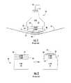
- FIG. 1is a cross-sectional schematic view of a light emitting diode broadly designated at 20 and illustrated in a manner that illustrates the potential problems than can arise when light emitting diodes mounted in certain orientations.
- the light emitting diode 20is shown in fairly simplified fashion, it will be understood by those of ordinary skill in this art that the device 20 can be more sophisticated (i.e. include more elements) than illustrated herein. In the present circumstances, however, the invention can be clearly understood using basic illustrations.
- An exemplary diode of the type illustrated at 20 and some of its variationsare also described in commonly assigned and co-pending application Publication No. US 20020123164, the contents of which are incorporated entirely herein by reference.
- the diode 20includes a substrate 21 which may be n-type silicon carbide having a polytype selected from the group consisting of the 2H, 4H, 6H, 8H,15R, and 3C polytypes of silicon carbide.
- the diode portion of the device 20is illustrated by the respective n-type gallium nitride region 22 and p-type gallium nitride region 23 , which together define a p-n junction 24 .
- Region 22 and region 23may each comprise a single layer or a group of related layers having different compositions, thicknesses, dopant concentrations or other qualities.
- the diode 20also includes an ohmic contact 25 to the p-type gallium nitride epitaxial region 23 and a die attach metal 26 in electrical contact with the ohmic contact.
- the die attach metal 26may physically contact a bond pad (not shown) such as a gold or silver layer.
- a bond padsuch as a gold or silver layer.
- reflector, barrier, and other metal layersmay be formed between die attach metal 26 and the ohmic contact 25 .
- Ohmic contact 15may be formed on substrate 21 to form a vertical device as described above, and a wire lead 29 may be connected to contact 15 for connecting the device to an external circuit.
- a passivation layer 5comprising an insulating material such as silicon nitride or silicon dioxide covers or an insulating polymer such as polyamide and protects the exposed surfaces of the epitaxial regions 22 , 23 .
- the diode 20is typically mounted on a metal or metallized lead frame 27 , which provides an electrical contact between the diode 20 and an external circuit.
- the die attach metal 26is formed of a metal that melts at a relatively low temperature, e.g., lower than the ohmic contact 25 and low enough such that other package components are not damaged during the die attach process. Accordingly, die attach metal 26 may comprise a solder such as tin or an alloy such as gold/tin.
- the die attach metalpermits the diode 20 to be mounted on the lead frame quickly and easily via soldering or thermosonic bonding. In this regard, FIG.
- FIG. 1also illustrates that if the die attach metal is formed imprecisely (which is always a possibility given the very small scale and size of most devices) a portion 30 of the die attach metal 26 can extend beyond the desired contact with the ohmic contact 25 and can contact the p-type gallium nitride region 23 or the n-type gallium nitride region 22 .
- the imprecise or unwanted portion 30 of the die attach metalmay contact n-type gallium nitride layer 22 and can form an unwanted and parasitic Schottky diode with the n-type layer 22 , or if it extends far enough, with the n-type silicon carbide substrate 21 .
- FIG. 2illustrates a conventional manner of defining or isolating a junction in a light-emitting diode.
- the diode(broadly designated at 32 ) has been illustrated in its most fundamental aspects and can include additional elements that for the sake of clarity are not illustrated in FIG. 2 .
- the diode 32includes an n-type silicon carbide substrate 33 , an n-type epitaxial layer of gallium nitride 34 on the substrate 33 , and a p-type layer of gallium nitride 35 on the n-type layer, and defining the p-n junction 36 .
- the epitaxial layers 34 and 35are typically etched to form the mesa structure illustrated in the right-hand portion of FIG. 2 , which also shows an ohmic contact 37 to the p-type epitaxial layer 35 .
- the junction 36 within the mesa formed by etching the layers 34 and 35is covered with silicon dioxide or some other appropriate insulating or dielectric material to help protect the junction 36 from external contamination and/or damage during die separation, packaging, or other processing steps, or during operation.
- a number of additional stepsmust be carried out. These typically include a masking step to define the pattern for the etch, which in turn includes the steps of laying down the mask (typically a photoresist), placing the optical pattern over the photoresist, exposing, and developing the resist, removing the developed (or as the case may be, undeveloped) portions of the mask and etching the underlying epitaxial layers, then removing the photoresist.
- a masking stepto define the pattern for the etch, which in turn includes the steps of laying down the mask (typically a photoresist), placing the optical pattern over the photoresist, exposing, and developing the resist, removing the developed (or as the case may be, undeveloped) portions of the mask and etching the underlying epitaxial layers, then removing the photoresist.
- FIG. 3is a broad schematic illustration of a junction-defining method of embodiments of the present invention.
- the methodcomprises implanting ions represented schematically by the arrows 40 into an epitaxial layer 41 in the diode broadly designated at 42 adjacent the p-n junction 43 .
- Epitaxial layer 41has a first conductivity type (illustrated in FIG. 3 as p-type).
- the type and amount of the implanted ionsincrease the resistivity of implanted region 44 and may render the implanted region 44 highly resistive and/or semi-insulating.
- “highly resistive”means that the material is sufficiently resistive such that negligible current flow occurs when a voltage bias is applied to the anodes of adjacent die on a wafer.
- the material in implanted regions 44is considered highly resistive for purposes of this invention if it substantially electrically isolates adjacent die.
- the resistivity of the implanted regions 44is at least 2000 ⁇ -cm. If the resistivity of the material is sufficiently high, the material may be considered semi-insulating (or “i-type”) material rather than p-type or n-type semiconductor material. In general, material having a resistivity in excess of 1 ⁇ 10 5 ⁇ -cm at room temperature may be considered semi-insulating for purposes of this invention.
- the ions 40may be implanted in a pattern that defines an implanted perimeter 44 as more clearly illustrated in FIG. 3A .
- the perimeter 44may be sufficiently doped with the implanted ions 40 to be highly resistive to thereby isolate or define the junction 43 with the implanted perimeter 44 .
- FIG. 3also illustrates the n-type layer 45 , the substrate 46 , and the metal contact 47 .
- the dashed lines in the epitaxial layer 41also help illustrate the location of the perimeter in the view of FIG. 3 .
- substrate 46may comprise n-type silicon carbide having a polytype selected from the group consisting of the 2H, 4H, 6H, 8H, 15R, and 3C polytypes of silicon carbide. It will be appreciated by those skilled in the art, however, that substrate 46 could comprise another material such as sapphire, gallium nitride, aluminum nitride or another suitable material such as MgO, spinel, silicon or ZnO. Moreover, the substrate 46 may be conductive to permit the formation of a vertical device, or the substrate 46 could be insulating or semi-insulating.
- metal contact 47may serve as the implant mask for implanting ions 40 into the device.
- metal contact 47comprises a metal stack with sufficient thickness to prevent ions 40 from reaching layer 41 , then it may be possible to avoid depositing a separate implant mask.
- the methodcomprises implanting ions such as nitrogen or phosphorus in the p-type layer of gallium nitride.
- ionssuch as nitrogen or phosphorus
- Other ionscan be used to increase the resistivity of the region via implantation, including hydrogen, helium, aluminum and N 2 .
- Other aspects of the methodwill be illustrated with respect to FIG. 5 .
- the implantationcan be carried out in conventional fashion and at room temperature.
- the implanting ionscreate damage within the GaN to produce deep levels within the bandgap. These in turn trap free carriers in the GaN thus rendering the material highly resistive.
- Light-emitting diodes in Group III nitrides such as GaNare not limited to using n-type substrates and p-type top layers. There are, however, a number of reasons, well understood in this art, as to why n-type SiC substrates are more commonly used. Thus, the invention could also include implanting an n-type layer to increase its resistivity. Because the use of n-type substrates is more common, however, most of the description herein will refer to such structures.
- diode 42can include one or more quantum wells, or superlattice structures or both and that the active layer or layers can include a greater range of the Group III nitride compounds than gallium nitride standing alone.
- active layersmay also be referred to as, “active layers,” “diode portions,” “diode regions,” or “diode structures,” without departing from the scope of the present invention.
- FIG. 4is a schematic cross sectional diagram similar to FIG. 1 , but illustrating a diode broadly designated at 50 that incorporates the implanted perimeter region 54 of the present invention.
- the diode 50includes a substrate, 51 which in some embodiments is n-type silicon carbide.
- An n-type gallium nitrite epitaxial layeris on the substrate 51 , and appears underneath the substrate 51 in the “flip-chip” orientation illustrated in FIG. 4 .
- the p-type layer 53is adjacent the n-type layer 52 and the two layers define a p-n junction 58 between them.
- the diodealso includes the ohmic contact 55 , and the die attach metal portion 56 .
- the diodehas been implanted in the manner just described with respect to FIG. 3 , it includes the highly resistive perimeter portions 54 shown adjacent the dotted lines in FIG. 4 .
- a portion 60 of less than ideally placed die attachment metalis also illustrated 54 on the lead frame 57 .
- the inventionprovides several advancements. First, the geometric spatial area available for the metal portion 60 is now more limited because the implanted regions 54 of the diode 50 do not require the multiple steps necessary to form a mesa. Thus, the p-type layer and its insulated portions 54 provide an additional geometric, spatial blocking of the excess metal 60 . Additionally, because the implanted portions 54 are highly resistive, there is little or no electrical interaction between the excess metal 60 and the implanted perimeter portions 54 .
- the inventionprovides a greater margin for error when using a standard or defined amount of die attachment metal 56 , 60 .
- the diode 50would have both anode and cathode connections to the lead frame but the details of these connections have been eliminated to clarify the illustration of the invention.
- the substrate 51is illustrated in FIG. 4 as being formed of conductive silicon carbide, but can also comprise semi-insulating silicon carbide or sapphire (which is insulating), because the advantages of the invention are based upon advantages provided in the epitaxial layers.
- an insulating or semi-insulating substraterequires a slightly different geometry than a conductive SiC substrate for packaging purposes, the principles with respect to the invention and the epitaxial layers remain the same.
- the substrate 51is preferably substantially transparent to the light emitted by the junction 58 when a potential difference is applied to the device.
- the substrateis preferably substantially transparent to light having wavelengths of between about 390 and 550 nanometers, and more preferably between about 485 and 550 nanometers.
- the semiinsulating border portions 54have sufficient resistivity to preclude Schottky behavior when the border 54 is in contact with the metal 56 , 60 that would otherwise produce Schottky behavior if the border 54 were n-type.
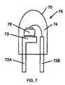
- a light emitting diode 78 of the invention and of the type illustrated in FIG. 3 or FIG. 4can be mounted in a package comprising a header 73 , electrical leads 72 , and an encapsulant 74 (such as epoxy) which may be molded in the shape of a lens 75 .
- LED 78may be mounted in a conventional substrate-down orientation or in a “flip-chip” orientation with the epitaxial layers adjacent the header 73 .
- the resulting LED lamp 79can be incorporated as part of a display or can be used as an indicator light, backlight or other application.
- the ohmic contacts to the p-type layerare typically selected from the group consisting of platinum, nickel, gold, titanium, aluminum, silver, and combinations of these, and when an ohmic contact is made to the silicon carbide substrate, it is usually selected from the group consisting of nickel, platinum, palladium, aluminum, titanium, and combinations thereof. Because the ohmic contacts to the substrate (not illustrated in FIG. 4 ) are visibly located in the direction in which light is desirably emitted, and because larger contacts have current-spreading advantages, the ohmic contact is preferably selected and formed to be as close to transparent as possible, typically with an additional smaller bonding pad being added to enhance the flow of current to the appropriate circuit.
- the ohmic contacts 55 and the die attach metal 56can be selected to act as a mirror or reflector to enhance the eventual output or the diode 50 when packaged and in use.
- additional metal layeror layers
- other metal layersmay be included in the metal stack for other purposes, such as barrier layers for preventing diffusion of contaminants and bonding layers for bonding external contacts to the device.
- the structure of the inventionis not limited to the schematic illustration of FIG. 4 .
- a buffer layeris often included as part of the structure between the silicon carbide substrate and the first gallium nitride (or other Group III nitride) layer.
- the buffer layercan comprise aluminum nitride, or a graded layer of aluminum gallium nitride (AlGaN) that progresses from a higher aluminum concentration near the silicon carbide substrate to a higher gallium nitride concentration at its interface with the gallium nitride epitaxial layer.
- AlGaNaluminum gallium nitride
- Other structural portions that can be incorporated into diodes of this type and with which the invention is particularly suitableinclude superlattice structures for enhancing the overall crystal stability of the device, quantum wells for enhancing the output of light or tuning it to a particular frequency, or multiple quantum wells for enhancing the brightness of the device by providing the additional number of active layers and the relationships between them.
- FIG. 5illustrates some of the method aspects of the invention.
- the methodelectrically defines or isolates a p-n junction in a diode, most preferably in a Group III nitride or gallium nitride-based diode, to minimize or avoid undesired electrical contacts and pathways when the diode is mounted for use and/or to prevent damage to the p-n junction during die separation.
- the methodcomprises depositing an ohmic metal contact layer on a central portion of a p-type epitaxial layer of gallium nitride that is part of a p-n junction, patterning the metal layer by applying an etch mask on the metal layer and removing a portion of the etch mask and the metal layer, and then implanting ions into the perimeter portions of the p-type epitaxial layer that are not covered by the etch mask.
- the methodcan comprise masking a portion of the ohmic metal layer (and potentially a bond pad on the ohmic contact), removing the remaining exposed ohmic metal contact layer from the epitaxial layer, implanting the exposed portions of epitaxial layer with atoms sufficient to increase the resistivity of the exposed portions (and potentially render the exposed portions semi-insulating), and removing the mask from the ohmic contact (and the bond pad) to thereby produce high-resistivity portions of the p-type layer.
- the methodcan comprise depositing the ohmic contact and the bond pad prior to the masking step, and masking the ohmic contact metal with the photoresist.
- the diode precursor 60includes a substrate 61 (which in certain embodiments comprises n-type SiC), an n-type gallium nitride epitaxial layer 62 on the substrate 61 , a p-type gallium nitride epitaxial layer 63 on the n-type layer 62 , an ohmic contact layer 65 on the p-type layer 63 , and a metal bond pad 66 on the ohmic contact layer 65 .
- the various steps of forming the substrate and epitaxial layers and depositing the ohmic contact and bond padare generally well understood in the art and will not be described in detail herein. Representative descriptions are included in issued patents including but not limited to commonly assigned U.S. Pat. Nos. 6,297,522; 6,217,662; 6,063,186; 5,679,153; 5,393,993; and 5,119,540.
- FIG. 5(B)illustrates the diode precursor 60 after a photoresist has been deposited, masked, and patterned to form the photoresist portion 67 on all of the bond pad as illustrated in FIG. 5(B) and some, but not all, areas of the ohmic contact 65 .
- the precursor in FIG. 5(B)is then etched to remove the portions of the ohmic contact layer 65 that are not covered by the photoresist 67 .
- the etchingcan be carried out in any appropriate manner, with reactive ion etching (RIE) using a chlorine-based plasma being a possible method.
- RIEreactive ion etching
- FIG. 5(C)in which the size of the ohmic contact has been reduced to an area represented as 65 ( a ).
- FIG. 5(C)also illustrates that with a portion of the ohmic contact layer 65 removed, portions of the p-type epitaxial gallium nitride layer are uncovered.
- FIG. 5(D)thus shows the implantation (schematically) of ions 70 to form the highly resistive regions 71 in the p-type gallium nitride layer 63 that define and isolate the junction 64 .
- the highly resistive implanted regions 71are semi-insulating.
- the implant step illustrated in FIG. 5(D)may be performed prior to the step of etching the ohmic contact layer 65 if the ohmic contact layer 65 is sufficiently thin so as not to substantially interfere with the implantation step.
- the precursor structure illustrated in FIG. 5(E)results.
- the precursor structuresmay then be separated into individual die.
- the method of the inventionreduces fabrication cycle time, wafer handling and chemical consumption, and likewise reduces the yield loss otherwise associated with the masking and etching procedures.
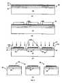
- a wafer 80comprising a substrate 81 and epitaxial regions 82 and 83 is provided.
- a metal stack 86is formed on epitaxial region 83 .
- epitaxial region 83has a first conductivity type and epitaxial region 82 has a second conductivity type opposite the first conductivity type.
- Each epitaxial region 82 and 83may comprise one or more layers having the same conductivity type.
- Metal stack 86may comprise a number of metal layers, each of which has a particular function.
- metal stack 86may comprise a layer of metal for forming an ohmic contact with epitaxial region 83 .
- Metal stack 86may also comprise reflector, barrier, adhesion, bonding, and/or other layers.
- etch mask 85is deposited on metal stack 86 and patterned via photolithography to form openings that selectively reveal surface portions 86 A of metal stack 86 .
- metal stack 86could be formed by photolithography, deposition and liftoff techniques which are well known in the art. That is, metal stack 86 could be formed by applying a blanket photoresist to the surface of the epitaxial region 83 , patterning the photoresist by exposing and developing it, depositing the metal as a blanket layer and lifting off the unwanted metal.
- metal stack 86is selectively etched to reveal surface portions 83 A of epitaxial region 83 .
- Etch mask 85is then removed by conventional methods.
- Ions 87are then implanted into the exposed portions of epitaxial region 83 to render the implanted regions 84 highly resistive in the manner described above and to define p-n junction regions 88 within the structure.
- the patterned metal layer 86serves as the implant mask.
- the etch/implant mask 85is removed and individual die 89 are separated using conventional techniques such that defined p-n junction regions 88 are spaced apart from the sidewalls 90 of the die, and are thereby physically and electrically isolated.
- an LED precursorcomprising an n-type silicon carbide substrate, an n-type epitaxial region and a p-type epitaxial region was provided.
- the p-type epitaxial regioncomprised GaN/AlGaN layers doped with Mg at a carrier concentration of about 1 to 5 ⁇ 1017 cm ⁇ 3 and had a total thickness of about 210 nm.
- N +1 nitrogenwas implanted at 20 keV at a dosage of 10 13 cm ⁇ 2 followed by a dosage at 125 keV of monovalent nitrogen at 1.4 ⁇ 10 13 cm ⁇ 2 .
- the first dosagewas carried out at 20 keV using N +1 at a dosage of 10 13 cm ⁇ 2 , followed by 125 keV of at a dosage of 1.4 ⁇ 10 13 cm ⁇ b 2 followed by 190 keV of N +1 at 1.7 ⁇ 10 13 cm ⁇ 2 .
- junction isolationwas verified by probing adjacent metal stacks and performing a continuity measurement. No measurable current was observed prior to breakdown of the p-n junction. Implanted helium and hydrogen have also created resistivity conditions leading to the potential conclusion that implanting almost any ion into p-type gallium nitride at room temperature will cause the material to become dramatically more resistant.
- junction isolationby this technique appears to lend itself to any nitride device that incorporates a p-type layer. For this reason, nitride based light emitting diodes on sapphire as well as on silicon carbide and other substrates appear to benefit equally from the use of implantation for junction isolation.
- the standard implant conditionwas (1) below. Other conditions (2)-(5). were also examined.
- the (2) conditionwas intended to evaluate the number of carriers that are eliminated per implanted ion.
- Conditions (3) and (5)were intended to evaluate the effect of implanting on the p-side of the device only.
- Condition (4)evaluated the efficiency of trapping carriers similar to the (1) and (2) comparison. In carrying out the implantations, it was determined that higher energy implants were needed for Cree's green LEDs as compared to Cree's blue LEDs.
- the 190 keV implant of (1) and (2)goes far deeper than the p-n junction placing most of the 190 keV implanted nitrogen on the n-side.
- the single dose at 125 keV of (3) and (4) and the double dose of (5)were considered.
- the 100 and 125 keV energiesplace the peak of the nitrogen concentration at or about the p-n junction which is 1500-1800 A below the surface.
- the simulated peak for the 100 and 125 keV implantsis about 1600 and 2000 A, respectively.
- the GaN materialis converted from low resistivity to high resistivity.
- P-type GaNis about 1200-1500 A thick with a free hole concentration of about 2-5 E17/cm 3
- P-type AlGaNis about 300 A thick with a hole concentration of about 5-20 E16/cm 3
- Condition (1)always worked for the blue LEDs (i.e., desired isolation and electrostatic discharge (ESD) yield).
- Condition (3)isolates the devices with good ESD yield.
- each of conditions (1)-(5)created high resistivity p-type material and isolated adjacent devices, but none produced good ESD yield.
- the addition of a further 230 keV nitrogen implant with a dose of 2 E 13/cm 2worked well for isolation and ESD yield.
- the resistivitywas estimated to be greater than 2 ⁇ 10 3 ohm-cm. This was done by evaluating the current flowing between two adjacent pads with an applied voltage of 2 Volts. The resulting current was unmeasurable ( ⁇ 50 nA). This corresponds to a resistance greater than 40 ⁇ 10 6 ohms. The distance between the pads is 70 microns and the width is 230 microns. The number of squares is then about 0.3 between them. The effects of fringing were ignored to give the estimate a worst case lower limit on resistivity. This gives a lower limit on the sheet resistance of 133 ⁇ 10 6 ohms per square. Taking the thickness to be 0.15 ⁇ 10 ⁇ 4 cm thick yields a resistivity of greater than 2000 ohm-cm.
Landscapes
- Led Devices (AREA)
- Recrystallisation Techniques (AREA)
- Led Device Packages (AREA)
Abstract
Description
- 1e13@20 keV, 1.4e13@125 keV, 1.7e13@190 keV (standard triple dose condition)
- 1e12@20 keV, 1.4e12@125 keV, 1.7e12@190 keV (standard condition @ 1/10 dose)
- 1.4e13@125 keV (single dose from standard condition of #1)
- 1.4e12@125 keV ( 1/10 dose of #4)
- 1e13 @30 keV, 1.4e13@100 keV
Claims (18)
Priority Applications (3)
| Application Number | Priority Date | Filing Date | Title |
|---|---|---|---|
| US10/840,463US7338822B2 (en) | 2003-05-09 | 2004-05-06 | LED fabrication via ion implant isolation |
| US11/154,619US7592634B2 (en) | 2004-05-06 | 2005-06-16 | LED fabrication via ion implant isolation |
| US12/507,288US7943954B2 (en) | 2004-05-06 | 2009-07-22 | LED fabrication via ion implant isolation |
Applications Claiming Priority (2)
| Application Number | Priority Date | Filing Date | Title |
|---|---|---|---|
| US32018203P | 2003-05-09 | 2003-05-09 | |
| US10/840,463US7338822B2 (en) | 2003-05-09 | 2004-05-06 | LED fabrication via ion implant isolation |
Related Child Applications (1)
| Application Number | Title | Priority Date | Filing Date |
|---|---|---|---|
| US11/154,619ContinuationUS7592634B2 (en) | 2004-05-06 | 2005-06-16 | LED fabrication via ion implant isolation |
Publications (3)
| Publication Number | Publication Date |
|---|---|
| US20050029533A1 US20050029533A1 (en) | 2005-02-10 |
| US20060108595A9 US20060108595A9 (en) | 2006-05-25 |
| US7338822B2true US7338822B2 (en) | 2008-03-04 |
Family
ID=33449503
Family Applications (1)
| Application Number | Title | Priority Date | Filing Date |
|---|---|---|---|
| US10/840,463Expired - LifetimeUS7338822B2 (en) | 2003-05-09 | 2004-05-06 | LED fabrication via ion implant isolation |
Country Status (6)
| Country | Link |
|---|---|
| US (1) | US7338822B2 (en) |
| EP (1) | EP1623467B1 (en) |
| JP (2) | JP5122817B2 (en) |
| CN (2) | CN101697366B (en) |
| TW (1) | TWI347683B (en) |
| WO (1) | WO2004102686A1 (en) |
Cited By (18)
| Publication number | Priority date | Publication date | Assignee | Title |
|---|---|---|---|---|
| US20080121908A1 (en)* | 2004-04-07 | 2008-05-29 | Shu Yuan | Fabrication of Reflective Layer on Semconductor Light Emitting Devices |
| US20080128722A1 (en)* | 2004-03-15 | 2008-06-05 | Shu Yuan | Fabrication of Semiconductor Devices |
| US20080164480A1 (en)* | 2003-09-19 | 2008-07-10 | Xuejun Kang | Fabrication of Semiconductor Devices |
| US20080210970A1 (en)* | 2003-09-19 | 2008-09-04 | Tinggi Technologies Private Limited | Fabrication of Conductive Metal Layer on Semiconductor Devices |
| US20080210969A1 (en)* | 2005-09-29 | 2008-09-04 | Tinggi Technologies Private Limited | Fabrication of Semiconductor Devices for Light Emission |
| US20080224173A1 (en)* | 2005-10-19 | 2008-09-18 | Tinggi Technologies Private Limited | Fabrication Transistors |
| US20100047996A1 (en)* | 2005-12-20 | 2010-02-25 | Tinggi Technologies Private Limited | Localized annealing during semiconductor device fabrication |
| US20100117107A1 (en)* | 2006-09-04 | 2010-05-13 | Shu Yuan | Electrical current distribution in light emitting devices |
| US7772604B2 (en) | 2006-01-05 | 2010-08-10 | Illumitex | Separate optical device for directing light from an LED |
| US7789531B2 (en) | 2006-10-02 | 2010-09-07 | Illumitex, Inc. | LED system and method |
| US7829358B2 (en) | 2008-02-08 | 2010-11-09 | Illumitex, Inc. | System and method for emitter layer shaping |
| US8096671B1 (en) | 2009-04-06 | 2012-01-17 | Nmera, Llc | Light emitting diode illumination system |
| US8115217B2 (en) | 2008-12-11 | 2012-02-14 | Illumitex, Inc. | Systems and methods for packaging light-emitting diode devices |
| US8395167B2 (en) | 2006-08-16 | 2013-03-12 | Tinggi Technologies Private Limited | External light efficiency of light emitting diodes |
| US8449128B2 (en) | 2009-08-20 | 2013-05-28 | Illumitex, Inc. | System and method for a lens and phosphor layer |
| US8585253B2 (en) | 2009-08-20 | 2013-11-19 | Illumitex, Inc. | System and method for color mixing lens array |
| US8664027B2 (en) | 2011-02-11 | 2014-03-04 | Varian Semiconductor Associates, Inc. | LED mesa sidewall isolation by ion implantation |
| US8692267B2 (en) | 2004-09-22 | 2014-04-08 | Cree, Inc. | High efficiency Group III nitride LED with lenticular surface |
Families Citing this family (29)
| Publication number | Priority date | Publication date | Assignee | Title |
|---|---|---|---|---|
| WO2004102686A1 (en)* | 2003-05-09 | 2004-11-25 | Cree, Inc. | Led fabrication via ion implant isolation |
| JP4766845B2 (en)* | 2003-07-25 | 2011-09-07 | シャープ株式会社 | Nitride-based compound semiconductor light-emitting device and method for manufacturing the same |
| US20050194584A1 (en)* | 2003-11-12 | 2005-09-08 | Slater David B.Jr. | LED fabrication via ion implant isolation |
| US7592634B2 (en)* | 2004-05-06 | 2009-09-22 | Cree, Inc. | LED fabrication via ion implant isolation |
| JP2008041811A (en)* | 2006-08-03 | 2008-02-21 | Ngk Spark Plug Co Ltd | Wiring board, multi-cavity wiring board, and manufacturing method thereof |
| US7646024B2 (en)* | 2006-08-18 | 2010-01-12 | Cree, Inc. | Structure and method for reducing forward voltage across a silicon carbide-group III nitride interface |
| US8674593B2 (en)* | 2007-05-31 | 2014-03-18 | Nthdegree Technologies Worldwide Inc | Diode for a printable composition |
| US20090261346A1 (en)* | 2008-04-16 | 2009-10-22 | Ding-Yuan Chen | Integrating CMOS and Optical Devices on a Same Chip |
| JP2010199558A (en)* | 2009-01-27 | 2010-09-09 | Panasonic Corp | Semiconductor device and method of manufacturing the same |
| US8263422B2 (en)* | 2010-04-26 | 2012-09-11 | Varian Semiconductor Equipment Associates, Inc. | Bond pad isolation and current confinement in an LED using ion implantation |
| DE102010026518B4 (en) | 2010-07-08 | 2025-02-27 | OSRAM Opto Semiconductors Gesellschaft mit beschränkter Haftung | Light-emitting diode chip and method for producing a plurality of light-emitting diode chips |
| KR101782081B1 (en)* | 2010-08-30 | 2017-09-26 | 엘지이노텍 주식회사 | Light emitting device |
| US20120097918A1 (en)* | 2010-10-20 | 2012-04-26 | Varian Semiconductor Equipment Associates, Inc. | Implanted current confinement structure to improve current spreading |
| US8927999B2 (en)* | 2011-11-21 | 2015-01-06 | Avogy, Inc. | Edge termination by ion implantation in GaN |
| DE102012108883A1 (en)* | 2012-09-20 | 2014-03-20 | Osram Opto Semiconductors Gmbh | Optoelectronic semiconductor chip and method for producing optoelectronic semiconductor chips |
| TWI495154B (en)* | 2012-12-06 | 2015-08-01 | Genesis Photonics Inc | Semiconductor structure |
| US9985190B2 (en)* | 2016-05-18 | 2018-05-29 | eLux Inc. | Formation and structure of post enhanced diodes for orientation control |
| CN106711301B (en)* | 2015-11-12 | 2020-10-27 | 美科米尚技术有限公司 | Light emitting diode and manufacturing method thereof |
| CN106024623B (en)* | 2016-06-29 | 2019-03-01 | 江苏能华微电子科技发展有限公司 | A kind of gallium nitride Schottky diode and preparation method thereof |
| TWI703726B (en) | 2016-09-19 | 2020-09-01 | 新世紀光電股份有限公司 | Semiconductor device containing nitrogen |
| US10892137B2 (en)* | 2018-09-12 | 2021-01-12 | Entegris, Inc. | Ion implantation processes and apparatus using gallium |
| DE102019129619A1 (en)* | 2019-11-04 | 2021-05-06 | OSRAM Opto Semiconductors Gesellschaft mit beschränkter Haftung | OPTOELECTRONIC SEMI-CONDUCTOR COMPONENT |
| GB2590450B (en)* | 2019-12-18 | 2022-01-05 | Plessey Semiconductors Ltd | Light emitting diode precursor |
| CN111653565B (en)* | 2020-03-11 | 2023-03-17 | 厦门市三安集成电路有限公司 | High-impedance semiconductor resistor structure and preparation method thereof |
| US11227801B2 (en) | 2020-03-19 | 2022-01-18 | International Business Machines Corporation | Formation of contacts for semiconductor devices |
| EP3971981A1 (en) | 2020-09-22 | 2022-03-23 | Samsung Electronics Co., Ltd. | Light-emitting diode display device and manufacturing method thereof |
| CN114864760B (en)* | 2021-02-03 | 2024-12-13 | 厦门三安光电有限公司 | Micro LEDs and display panels |
| CN114141916B (en)* | 2021-11-24 | 2023-08-01 | 福州大学 | Nanometer-sized LED chip array and preparation method thereof |
| CN114628432B (en)* | 2022-02-28 | 2023-03-10 | 诺视科技(苏州)有限公司 | Manufacturing method of semiconductor device and semiconductor device |
Citations (37)
| Publication number | Priority date | Publication date | Assignee | Title |
|---|---|---|---|---|
| US3824133A (en) | 1971-12-02 | 1974-07-16 | Bell Telephone Labor Inc | Fabrication of electrically insulating regions in optical devices by proton bombardment |
| US4968582A (en) | 1988-06-28 | 1990-11-06 | Mcnc And University Of Nc At Charlotte | Photoresists resistant to oxygen plasmas |
| US5091757A (en) | 1989-09-07 | 1992-02-25 | Ricoh Company, Ltd. | Semiconductor light emitting array with particular surfaces |
| US5114827A (en) | 1988-06-28 | 1992-05-19 | Microelectronics Center Of N.C. | Photoresists resistant to oxygen plasmas |
| US5119540A (en) | 1990-07-24 | 1992-06-09 | Cree Research, Inc. | Apparatus for eliminating residual nitrogen contamination in epitaxial layers of silicon carbide and resulting product |
| US5210051A (en)* | 1990-03-27 | 1993-05-11 | Cree Research, Inc. | High efficiency light emitting diodes from bipolar gallium nitride |
| US5248760A (en) | 1991-01-25 | 1993-09-28 | Unc At Charlotte | Chemically cured low temperature polyimides |
| US5393642A (en) | 1992-12-31 | 1995-02-28 | The University Of North Carolina At Charlotte | Ionic modification of organic resins and photoresists to produce photoactive etch resistant compositions |
| US5393993A (en) | 1993-12-13 | 1995-02-28 | Cree Research, Inc. | Buffer structure between silicon carbide and gallium nitride and resulting semiconductor devices |
| US5416342A (en) | 1993-06-23 | 1995-05-16 | Cree Research, Inc. | Blue light-emitting diode with high external quantum efficiency |
| US5635412A (en) | 1994-05-04 | 1997-06-03 | North Carolina State University | Methods of fabricating voltage breakdown resistant monocrystalline silicon carbide semiconductor devices |
| US5679153A (en) | 1994-11-30 | 1997-10-21 | Cree Research, Inc. | Method for reducing micropipe formation in the epitaxial growth of silicon carbide and resulting silicon carbide structures |
| US5718760A (en) | 1996-02-05 | 1998-02-17 | Cree Research, Inc. | Growth of colorless silicon carbide crystals |
| US5838706A (en) | 1994-09-20 | 1998-11-17 | Cree Research, Inc. | Low-strain laser structures with group III nitride active layers |
| US5866925A (en) | 1997-01-09 | 1999-02-02 | Sandia Corporation | Gallium nitride junction field-effect transistor |
| US5912477A (en) | 1994-10-07 | 1999-06-15 | Cree Research, Inc. | High efficiency light emitting diodes |
| US5914499A (en) | 1995-01-18 | 1999-06-22 | Abb Research Ltd. | High voltage silicon carbide semiconductor device with bended edge |
| US5998232A (en) | 1998-01-16 | 1999-12-07 | Implant Sciences Corporation | Planar technology for producing light-emitting devices |
| US6063186A (en) | 1997-12-17 | 2000-05-16 | Cree, Inc. | Growth of very uniform silicon carbide epitaxial layers |
| US6090300A (en) | 1998-05-26 | 2000-07-18 | Xerox Corporation | Ion-implantation assisted wet chemical etching of III-V nitrides and alloys |
| US6111273A (en)* | 1998-01-28 | 2000-08-29 | Sony Corporation | Semiconductor device and its manufacturing method |
| US6187606B1 (en) | 1997-10-07 | 2001-02-13 | Cree, Inc. | Group III nitride photonic devices on silicon carbide substrates with conductive buffer interlayer structure |
| US6204084B1 (en) | 1996-09-06 | 2001-03-20 | Kabushiki Kaisha Toshiba | Nitride system semiconductor device and method for manufacturing the same |
| US6217662B1 (en) | 1997-03-24 | 2001-04-17 | Cree, Inc. | Susceptor designs for silicon carbide thin films |
| US6255129B1 (en)* | 2000-09-07 | 2001-07-03 | Highlink Technology Corporation | Light-emitting diode device and method of manufacturing the same |
| US6278136B1 (en) | 1997-04-22 | 2001-08-21 | Kabushiki Kaisha Toshiba | Semiconductor light emitting element, its manufacturing method and light emitting device |
| US20020017727A1 (en) | 1998-12-22 | 2002-02-14 | Toyoda Gosei Co., Ltd. | Method for manufacturing semiconductor device using group III nitride compound |
| US20020093020A1 (en) | 2001-01-16 | 2002-07-18 | Edmond John Adam | Group III nitride LED with undoped cladding layer (5000.137) |
| US20020096496A1 (en) | 2000-11-29 | 2002-07-25 | Bela Molnar | Patterning of GaN crystal films with ion beams and subsequent wet etching |
| US6432788B1 (en) | 1999-07-22 | 2002-08-13 | Implant Sciences Corporation | Method for fabricating an emitter-base junction for a gallium nitride bipolar transistor |
| US20020123164A1 (en) | 2001-02-01 | 2002-09-05 | Slater David B. | Light emitting diodes including modifications for light extraction and manufacturing methods therefor |
| US6459100B1 (en) | 1998-09-16 | 2002-10-01 | Cree, Inc. | Vertical geometry ingan LED |
| US20020139987A1 (en)* | 2001-03-29 | 2002-10-03 | Collins William David | Monolithic series/parallel led arrays formed on highly resistive substrates |
| US20030008425A1 (en) | 2001-06-06 | 2003-01-09 | Toshiya Uemura | Method for producing group III nitride compound semiconductor light-emitting element |
| US20030015721A1 (en) | 2001-07-23 | 2003-01-23 | Slater, David B. | Light emitting diodes including modifications for submount bonding and manufacturing methods therefor |
| US6582986B2 (en) | 1999-10-14 | 2003-06-24 | Cree, Inc. | Single step pendeo-and lateral epitaxial overgrowth of group III-nitride epitaxial layers with group III-nitride buffer layer and resulting structures |
| US20050029533A1 (en)* | 2003-05-09 | 2005-02-10 | Yifeng Wu | LED fabrication via ion implant isolation |
Family Cites Families (7)
| Publication number | Priority date | Publication date | Assignee | Title |
|---|---|---|---|---|
| JPH0546052U (en)* | 1991-11-19 | 1993-06-18 | 三洋電機株式会社 | Light emitting diode device |
| JPH0697498A (en)* | 1992-09-17 | 1994-04-08 | Toshiba Corp | Semiconductor light emitting element |
| JP3516433B2 (en)* | 1997-12-19 | 2004-04-05 | 昭和電工株式会社 | Compound semiconductor light emitting device |
| JP2000077713A (en)* | 1998-08-27 | 2000-03-14 | Sanyo Electric Co Ltd | Semiconductor light-emitting element |
| JP3424634B2 (en)* | 2000-01-27 | 2003-07-07 | 日亜化学工業株式会社 | Nitride semiconductor laser device |
| JP2001237499A (en)* | 2000-02-22 | 2001-08-31 | Sony Corp | Manufacturing method of semiconductor light-emitting element |
| TW493284B (en)* | 2000-09-06 | 2002-07-01 | Highlink Technology Corp | LED device and the manufacturing method thereof |
- 2004
- 2004-05-06WOPCT/US2004/014023patent/WO2004102686A1/enactiveSearch and Examination
- 2004-05-06CNCN2009102088552Apatent/CN101697366B/ennot_activeExpired - Lifetime
- 2004-05-06CNCN2004800125618Apatent/CN1802755B/ennot_activeExpired - Lifetime
- 2004-05-06EPEP04751419.5Apatent/EP1623467B1/ennot_activeExpired - Lifetime
- 2004-05-06JPJP2006532792Apatent/JP5122817B2/ennot_activeExpired - Lifetime
- 2004-05-06USUS10/840,463patent/US7338822B2/ennot_activeExpired - Lifetime
- 2004-05-07TWTW093112923Apatent/TWI347683B/ennot_activeIP Right Cessation
- 2011
- 2011-03-15JPJP2011056687Apatent/JP5491439B2/ennot_activeExpired - Lifetime
Patent Citations (44)
| Publication number | Priority date | Publication date | Assignee | Title |
|---|---|---|---|---|
| US3824133A (en) | 1971-12-02 | 1974-07-16 | Bell Telephone Labor Inc | Fabrication of electrically insulating regions in optical devices by proton bombardment |
| US4968582A (en) | 1988-06-28 | 1990-11-06 | Mcnc And University Of Nc At Charlotte | Photoresists resistant to oxygen plasmas |
| US5114827A (en) | 1988-06-28 | 1992-05-19 | Microelectronics Center Of N.C. | Photoresists resistant to oxygen plasmas |
| US5091757A (en) | 1989-09-07 | 1992-02-25 | Ricoh Company, Ltd. | Semiconductor light emitting array with particular surfaces |
| US5210051A (en)* | 1990-03-27 | 1993-05-11 | Cree Research, Inc. | High efficiency light emitting diodes from bipolar gallium nitride |
| US5119540A (en) | 1990-07-24 | 1992-06-09 | Cree Research, Inc. | Apparatus for eliminating residual nitrogen contamination in epitaxial layers of silicon carbide and resulting product |
| US5248760A (en) | 1991-01-25 | 1993-09-28 | Unc At Charlotte | Chemically cured low temperature polyimides |
| US5393642A (en) | 1992-12-31 | 1995-02-28 | The University Of North Carolina At Charlotte | Ionic modification of organic resins and photoresists to produce photoactive etch resistant compositions |
| US5416342A (en) | 1993-06-23 | 1995-05-16 | Cree Research, Inc. | Blue light-emitting diode with high external quantum efficiency |
| US5393993A (en) | 1993-12-13 | 1995-02-28 | Cree Research, Inc. | Buffer structure between silicon carbide and gallium nitride and resulting semiconductor devices |
| US5635412A (en) | 1994-05-04 | 1997-06-03 | North Carolina State University | Methods of fabricating voltage breakdown resistant monocrystalline silicon carbide semiconductor devices |
| US5838706A (en) | 1994-09-20 | 1998-11-17 | Cree Research, Inc. | Low-strain laser structures with group III nitride active layers |
| US5912477A (en) | 1994-10-07 | 1999-06-15 | Cree Research, Inc. | High efficiency light emitting diodes |
| US5679153A (en) | 1994-11-30 | 1997-10-21 | Cree Research, Inc. | Method for reducing micropipe formation in the epitaxial growth of silicon carbide and resulting silicon carbide structures |
| US5914499A (en) | 1995-01-18 | 1999-06-22 | Abb Research Ltd. | High voltage silicon carbide semiconductor device with bended edge |
| US5718760A (en) | 1996-02-05 | 1998-02-17 | Cree Research, Inc. | Growth of colorless silicon carbide crystals |
| US6025289A (en) | 1996-02-05 | 2000-02-15 | Cree Research, Inc. | Colorless silicon carbide crystals |
| US6200917B1 (en) | 1996-02-05 | 2001-03-13 | Cree, Inc. | Colorless silicon carbide gemstones |
| US6204084B1 (en) | 1996-09-06 | 2001-03-20 | Kabushiki Kaisha Toshiba | Nitride system semiconductor device and method for manufacturing the same |
| US5866925A (en) | 1997-01-09 | 1999-02-02 | Sandia Corporation | Gallium nitride junction field-effect transistor |
| US6217662B1 (en) | 1997-03-24 | 2001-04-17 | Cree, Inc. | Susceptor designs for silicon carbide thin films |
| US6278136B1 (en) | 1997-04-22 | 2001-08-21 | Kabushiki Kaisha Toshiba | Semiconductor light emitting element, its manufacturing method and light emitting device |
| US6187606B1 (en) | 1997-10-07 | 2001-02-13 | Cree, Inc. | Group III nitride photonic devices on silicon carbide substrates with conductive buffer interlayer structure |
| US6373077B1 (en) | 1997-10-07 | 2002-04-16 | Cree, Inc. | Group III nitride photonic devices on silicon carbide substrates with conductive buffer interlayer structure |
| US6201262B1 (en) | 1997-10-07 | 2001-03-13 | Cree, Inc. | Group III nitride photonic devices on silicon carbide substrates with conductive buffer interlay structure |
| US6063186A (en) | 1997-12-17 | 2000-05-16 | Cree, Inc. | Growth of very uniform silicon carbide epitaxial layers |
| US6297522B1 (en) | 1997-12-17 | 2001-10-02 | Cree, Inc. | Highly uniform silicon carbide epitaxial layers |
| US5998232A (en) | 1998-01-16 | 1999-12-07 | Implant Sciences Corporation | Planar technology for producing light-emitting devices |
| US6235617B1 (en)* | 1998-01-28 | 2001-05-22 | Sony Corporation | Semiconductor device and its manufacturing method |
| US6111273A (en)* | 1998-01-28 | 2000-08-29 | Sony Corporation | Semiconductor device and its manufacturing method |
| US6090300A (en) | 1998-05-26 | 2000-07-18 | Xerox Corporation | Ion-implantation assisted wet chemical etching of III-V nitrides and alloys |
| US6459100B1 (en) | 1998-09-16 | 2002-10-01 | Cree, Inc. | Vertical geometry ingan LED |
| US20020017727A1 (en) | 1998-12-22 | 2002-02-14 | Toyoda Gosei Co., Ltd. | Method for manufacturing semiconductor device using group III nitride compound |
| US6432788B1 (en) | 1999-07-22 | 2002-08-13 | Implant Sciences Corporation | Method for fabricating an emitter-base junction for a gallium nitride bipolar transistor |
| US6582986B2 (en) | 1999-10-14 | 2003-06-24 | Cree, Inc. | Single step pendeo-and lateral epitaxial overgrowth of group III-nitride epitaxial layers with group III-nitride buffer layer and resulting structures |
| US6255129B1 (en)* | 2000-09-07 | 2001-07-03 | Highlink Technology Corporation | Light-emitting diode device and method of manufacturing the same |
| US20020096496A1 (en) | 2000-11-29 | 2002-07-25 | Bela Molnar | Patterning of GaN crystal films with ion beams and subsequent wet etching |
| US20020093020A1 (en) | 2001-01-16 | 2002-07-18 | Edmond John Adam | Group III nitride LED with undoped cladding layer (5000.137) |
| US20020123164A1 (en) | 2001-02-01 | 2002-09-05 | Slater David B. | Light emitting diodes including modifications for light extraction and manufacturing methods therefor |
| US6791119B2 (en)* | 2001-02-01 | 2004-09-14 | Cree, Inc. | Light emitting diodes including modifications for light extraction |
| US20020139987A1 (en)* | 2001-03-29 | 2002-10-03 | Collins William David | Monolithic series/parallel led arrays formed on highly resistive substrates |
| US20030008425A1 (en) | 2001-06-06 | 2003-01-09 | Toshiya Uemura | Method for producing group III nitride compound semiconductor light-emitting element |
| US20030015721A1 (en) | 2001-07-23 | 2003-01-23 | Slater, David B. | Light emitting diodes including modifications for submount bonding and manufacturing methods therefor |
| US20050029533A1 (en)* | 2003-05-09 | 2005-02-10 | Yifeng Wu | LED fabrication via ion implant isolation |
Non-Patent Citations (3)
| Title |
|---|
| Feldman et al., High Resistivity Group III-V Compounds By Helium Bombardment, Reg. No. H147, Nov. 4, 1986.* |
| J.C. Zolper et al, Nitrogen and fluorin ion implantation in InGaN, 1995, Applied Physics Letters, vol. 66, pp. 3042-3044.* |
| S. Wolf, Silicon Processing For VLSI ERA, vol. 1, Lattice Press, pp. 282.* |
Cited By (33)
| Publication number | Priority date | Publication date | Assignee | Title |
|---|---|---|---|---|
| US20080164480A1 (en)* | 2003-09-19 | 2008-07-10 | Xuejun Kang | Fabrication of Semiconductor Devices |
| US20080210970A1 (en)* | 2003-09-19 | 2008-09-04 | Tinggi Technologies Private Limited | Fabrication of Conductive Metal Layer on Semiconductor Devices |
| US8034643B2 (en) | 2003-09-19 | 2011-10-11 | Tinggi Technologies Private Limited | Method for fabrication of a semiconductor device |
| US20080128722A1 (en)* | 2004-03-15 | 2008-06-05 | Shu Yuan | Fabrication of Semiconductor Devices |
| US7763477B2 (en)* | 2004-03-15 | 2010-07-27 | Tinggi Technologies Pte Limited | Fabrication of semiconductor devices |
| US8309377B2 (en) | 2004-04-07 | 2012-11-13 | Tinggi Technologies Private Limited | Fabrication of reflective layer on semiconductor light emitting devices |
| US20080121908A1 (en)* | 2004-04-07 | 2008-05-29 | Shu Yuan | Fabrication of Reflective Layer on Semconductor Light Emitting Devices |
| US8878209B2 (en) | 2004-09-22 | 2014-11-04 | Cree, Inc. | High efficiency group III nitride LED with lenticular surface |
| US8692267B2 (en) | 2004-09-22 | 2014-04-08 | Cree, Inc. | High efficiency Group III nitride LED with lenticular surface |
| US8004001B2 (en) | 2005-09-29 | 2011-08-23 | Tinggi Technologies Private Limited | Fabrication of semiconductor devices for light emission |
| US20080210969A1 (en)* | 2005-09-29 | 2008-09-04 | Tinggi Technologies Private Limited | Fabrication of Semiconductor Devices for Light Emission |
| US8067269B2 (en) | 2005-10-19 | 2011-11-29 | Tinggi Technologies Private Limted | Method for fabricating at least one transistor |
| US20080224173A1 (en)* | 2005-10-19 | 2008-09-18 | Tinggi Technologies Private Limited | Fabrication Transistors |
| US8329556B2 (en) | 2005-12-20 | 2012-12-11 | Tinggi Technologies Private Limited | Localized annealing during semiconductor device fabrication |
| US20100047996A1 (en)* | 2005-12-20 | 2010-02-25 | Tinggi Technologies Private Limited | Localized annealing during semiconductor device fabrication |
| US7968896B2 (en) | 2006-01-05 | 2011-06-28 | Illumitex, Inc. | Separate optical device for directing light from an LED |
| US9574743B2 (en) | 2006-01-05 | 2017-02-21 | Illumitex, Inc. | Separate optical device for directing light from an LED |
| US8896003B2 (en) | 2006-01-05 | 2014-11-25 | Illumitex, Inc. | Separate optical device for directing light from an LED |
| US7772604B2 (en) | 2006-01-05 | 2010-08-10 | Illumitex | Separate optical device for directing light from an LED |
| US20100284167A1 (en)* | 2006-01-05 | 2010-11-11 | Duong Dung T | Separate optical device for directing light from an led |
| US8395167B2 (en) | 2006-08-16 | 2013-03-12 | Tinggi Technologies Private Limited | External light efficiency of light emitting diodes |
| US8124994B2 (en) | 2006-09-04 | 2012-02-28 | Tinggi Technologies Private Limited | Electrical current distribution in light emitting devices |
| US20100117107A1 (en)* | 2006-09-04 | 2010-05-13 | Shu Yuan | Electrical current distribution in light emitting devices |
| US8087960B2 (en) | 2006-10-02 | 2012-01-03 | Illumitex, Inc. | LED system and method |
| US7789531B2 (en) | 2006-10-02 | 2010-09-07 | Illumitex, Inc. | LED system and method |
| US8263993B2 (en) | 2008-02-08 | 2012-09-11 | Illumitex, Inc. | System and method for emitter layer shaping |
| US7829358B2 (en) | 2008-02-08 | 2010-11-09 | Illumitex, Inc. | System and method for emitter layer shaping |
| US8115217B2 (en) | 2008-12-11 | 2012-02-14 | Illumitex, Inc. | Systems and methods for packaging light-emitting diode devices |
| US8096671B1 (en) | 2009-04-06 | 2012-01-17 | Nmera, Llc | Light emitting diode illumination system |
| US8449128B2 (en) | 2009-08-20 | 2013-05-28 | Illumitex, Inc. | System and method for a lens and phosphor layer |
| US8585253B2 (en) | 2009-08-20 | 2013-11-19 | Illumitex, Inc. | System and method for color mixing lens array |
| US9086211B2 (en) | 2009-08-20 | 2015-07-21 | Illumitex, Inc. | System and method for color mixing lens array |
| US8664027B2 (en) | 2011-02-11 | 2014-03-04 | Varian Semiconductor Associates, Inc. | LED mesa sidewall isolation by ion implantation |
Also Published As
| Publication number | Publication date |
|---|---|
| JP5491439B2 (en) | 2014-05-14 |
| CN1802755B (en) | 2012-05-16 |
| JP2006528435A (en) | 2006-12-14 |
| EP1623467A1 (en) | 2006-02-08 |
| EP1623467B1 (en) | 2016-12-07 |
| JP2011187966A (en) | 2011-09-22 |
| CN1802755A (en) | 2006-07-12 |
| JP5122817B2 (en) | 2013-01-16 |
| TWI347683B (en) | 2011-08-21 |
| US20060108595A9 (en) | 2006-05-25 |
| CN101697366B (en) | 2012-12-19 |
| CN101697366A (en) | 2010-04-21 |
| WO2004102686A1 (en) | 2004-11-25 |
| US20050029533A1 (en) | 2005-02-10 |
| TW200501459A (en) | 2005-01-01 |
Similar Documents
| Publication | Publication Date | Title |
|---|---|---|
| US7338822B2 (en) | LED fabrication via ion implant isolation | |
| US7943406B2 (en) | LED fabrication via ion implant isolation | |
| US7943954B2 (en) | LED fabrication via ion implant isolation | |
| US6998642B2 (en) | Series connection of two light emitting diodes through semiconductor manufacture process | |
| JP4699258B2 (en) | Flip chip light emitting diode and manufacturing method thereof | |
| US20060060877A1 (en) | High efficiency group III nitride-silicon carbide light emitting diode | |
| US20060202225A1 (en) | Submount for use in flipchip-structured light emitting device including transistor | |
| WO2012091311A2 (en) | High efficiency light emitting diode | |
| KR100431760B1 (en) | AlGaInN LED device and their fabrication method | |
| KR101719623B1 (en) | Light emitting diode | |
| KR100609118B1 (en) | Flip Chip Light Emitting Diode and Manufacturing Method Thereof | |
| RU2523777C2 (en) | Extension of terminal pads to edge of chip with electrical insulation | |
| KR101203138B1 (en) | Luminous device and the method therefor | |
| KR101158071B1 (en) | Luminous element having arrayed cells and method of manufacturing the same | |
| KR101171356B1 (en) | Luminous element having arrayed cells and method of manufacturing the same | |
| KR100691497B1 (en) | Light-emitting device and Method of manufacturing the same | |
| KR101773582B1 (en) | High efficiency light emitting diode | |
| KR100663910B1 (en) | Light emitting device and manufacturing method thereof | |
| KR100646635B1 (en) | Single light emitting device of a plurality of cells and a method of manufacturing the same | |
| CN217387195U (en) | Flip-chip type MICROLED chip structure | |
| KR100663907B1 (en) | A light emitting device in which a plurality of cells are combined and a method of manufacturing the same | |
| KR100644215B1 (en) | Light emitting device and manufacturing method | |
| KR101633814B1 (en) | light emitting device |
Legal Events
| Date | Code | Title | Description |
|---|---|---|---|
| AS | Assignment | Owner name:CREE, INC., NORTH CAROLINA Free format text:ASSIGNMENT OF ASSIGNORS INTEREST;ASSIGNORS:WU, YIFENG;NEGLEY, GERALD H.;SLATER, DAVID B., JR.;AND OTHERS;SIGNING DATES FROM 20050920 TO 20051014;REEL/FRAME:016911/0797 Owner name:CREE, INC., NORTH CAROLINA Free format text:ASSIGNMENT OF ASSIGNORS INTEREST;ASSIGNORS:WU, YIFENG;NEGLEY, GERALD H.;SLATER, DAVID B., JR.;AND OTHERS;REEL/FRAME:016911/0797;SIGNING DATES FROM 20050920 TO 20051014 | |
| STCF | Information on status: patent grant | Free format text:PATENTED CASE | |
| FPAY | Fee payment | Year of fee payment:4 | |
| FPAY | Fee payment | Year of fee payment:8 | |
| MAFP | Maintenance fee payment | Free format text:PAYMENT OF MAINTENANCE FEE, 12TH YEAR, LARGE ENTITY (ORIGINAL EVENT CODE: M1553); ENTITY STATUS OF PATENT OWNER: LARGE ENTITY Year of fee payment:12 | |
| AS | Assignment | Owner name:CREE LED, INC., CALIFORNIA Free format text:ASSIGNMENT OF ASSIGNORS INTEREST;ASSIGNOR:CREE, INC.;REEL/FRAME:056012/0200 Effective date:20210301 | |
| AS | Assignment | Owner name:CITIZENS BANK, N.A., MASSACHUSETTS Free format text:SECURITY INTEREST;ASSIGNORS:SMART MODULAR TECHNOLOGIES, INC.;SMART HIGH RELIABILITY SOLUTIONS, LLC;SMART EMBEDDED COMPUTING, INC.;AND OTHERS;REEL/FRAME:058983/0001 Effective date:20220207 | |
| AS | Assignment | Owner name:SMART MODULAR TECHNOLOGIES, INC., CALIFORNIA Free format text:RELEASE OF PATENT SECURITY INTEREST RECORDED AT R/F 058983/0001;ASSIGNOR:CITIZENS BANK, N.A.;REEL/FRAME:071725/0207 Effective date:20250624 Owner name:SMART EMBEDDED COMPUTING, INC., ARIZONA Free format text:RELEASE OF PATENT SECURITY INTEREST RECORDED AT R/F 058983/0001;ASSIGNOR:CITIZENS BANK, N.A.;REEL/FRAME:071725/0207 Effective date:20250624 Owner name:SMART HIGH RELIABILITY SOLUTIONS LLC, CALIFORNIA Free format text:RELEASE OF PATENT SECURITY INTEREST RECORDED AT R/F 058983/0001;ASSIGNOR:CITIZENS BANK, N.A.;REEL/FRAME:071725/0207 Effective date:20250624 Owner name:CREELED, INC., CALIFORNIA Free format text:RELEASE OF PATENT SECURITY INTEREST RECORDED AT R/F 058983/0001;ASSIGNOR:CITIZENS BANK, N.A.;REEL/FRAME:071725/0207 Effective date:20250624 | |
| AS | Assignment | Owner name:CREELED, INC., CALIFORNIA Free format text:CORRECTIVE ASSIGNMENT TO CORRECT THE NAME OF THE ASSIGNEE PREVIOUSLY RECORDED ON REEL 56012 FRAME 200. ASSIGNOR(S) HEREBY CONFIRMS THE ASSIGNMENT;ASSIGNOR:CREE, INC.;REEL/FRAME:071874/0001 Effective date:20210301 |