US7336752B2 - Wide frequency range delay locked loop - Google Patents
Wide frequency range delay locked loopDownload PDFInfo
- Publication number
- US7336752B2 US7336752B2US10/335,535US33553502AUS7336752B2US 7336752 B2US7336752 B2US 7336752B2US 33553502 AUS33553502 AUS 33553502AUS 7336752 B2US7336752 B2US 7336752B2
- Authority
- US
- United States
- Prior art keywords
- delay
- clock signal
- locked loop
- response
- circuit
- Prior art date
- Legal status (The legal status is an assumption and is not a legal conclusion. Google has not performed a legal analysis and makes no representation as to the accuracy of the status listed.)
- Expired - Lifetime, expires
Links
Images


Classifications
- H—ELECTRICITY
- H03—ELECTRONIC CIRCUITRY
- H03L—AUTOMATIC CONTROL, STARTING, SYNCHRONISATION OR STABILISATION OF GENERATORS OF ELECTRONIC OSCILLATIONS OR PULSES
- H03L7/00—Automatic control of frequency or phase; Synchronisation
- H03L7/06—Automatic control of frequency or phase; Synchronisation using a reference signal applied to a frequency- or phase-locked loop
- H03L7/08—Details of the phase-locked loop
- H03L7/081—Details of the phase-locked loop provided with an additional controlled phase shifter
- H03L7/0812—Details of the phase-locked loop provided with an additional controlled phase shifter and where no voltage or current controlled oscillator is used
- H03L7/0816—Details of the phase-locked loop provided with an additional controlled phase shifter and where no voltage or current controlled oscillator is used the controlled phase shifter and the frequency- or phase-detection arrangement being connected to a common input
- H—ELECTRICITY
- H03—ELECTRONIC CIRCUITRY
- H03L—AUTOMATIC CONTROL, STARTING, SYNCHRONISATION OR STABILISATION OF GENERATORS OF ELECTRONIC OSCILLATIONS OR PULSES
- H03L7/00—Automatic control of frequency or phase; Synchronisation
- H03L7/06—Automatic control of frequency or phase; Synchronisation using a reference signal applied to a frequency- or phase-locked loop
- H03L7/08—Details of the phase-locked loop
- H03L7/085—Details of the phase-locked loop concerning mainly the frequency- or phase-detection arrangement including the filtering or amplification of its output signal
- H03L7/087—Details of the phase-locked loop concerning mainly the frequency- or phase-detection arrangement including the filtering or amplification of its output signal using at least two phase detectors or a frequency and phase detector in the loop
- H—ELECTRICITY
- H03—ELECTRONIC CIRCUITRY
- H03L—AUTOMATIC CONTROL, STARTING, SYNCHRONISATION OR STABILISATION OF GENERATORS OF ELECTRONIC OSCILLATIONS OR PULSES
- H03L7/00—Automatic control of frequency or phase; Synchronisation
- H03L7/06—Automatic control of frequency or phase; Synchronisation using a reference signal applied to a frequency- or phase-locked loop
- H03L7/08—Details of the phase-locked loop
- H03L7/081—Details of the phase-locked loop provided with an additional controlled phase shifter
- H03L7/0812—Details of the phase-locked loop provided with an additional controlled phase shifter and where no voltage or current controlled oscillator is used
- H03L7/0814—Details of the phase-locked loop provided with an additional controlled phase shifter and where no voltage or current controlled oscillator is used the phase shifting device being digitally controlled
- H—ELECTRICITY
- H03—ELECTRONIC CIRCUITRY
- H03L—AUTOMATIC CONTROL, STARTING, SYNCHRONISATION OR STABILISATION OF GENERATORS OF ELECTRONIC OSCILLATIONS OR PULSES
- H03L7/00—Automatic control of frequency or phase; Synchronisation
- H03L7/06—Automatic control of frequency or phase; Synchronisation using a reference signal applied to a frequency- or phase-locked loop
- H03L7/08—Details of the phase-locked loop
- H03L7/081—Details of the phase-locked loop provided with an additional controlled phase shifter
- H03L7/0812—Details of the phase-locked loop provided with an additional controlled phase shifter and where no voltage or current controlled oscillator is used
- H03L7/0818—Details of the phase-locked loop provided with an additional controlled phase shifter and where no voltage or current controlled oscillator is used the controlled phase shifter comprising coarse and fine delay or phase-shifting means
- H—ELECTRICITY
- H03—ELECTRONIC CIRCUITRY
- H03L—AUTOMATIC CONTROL, STARTING, SYNCHRONISATION OR STABILISATION OF GENERATORS OF ELECTRONIC OSCILLATIONS OR PULSES
- H03L7/00—Automatic control of frequency or phase; Synchronisation
- H03L7/06—Automatic control of frequency or phase; Synchronisation using a reference signal applied to a frequency- or phase-locked loop
- H03L7/08—Details of the phase-locked loop
- H03L7/10—Details of the phase-locked loop for assuring initial synchronisation or for broadening the capture range
- H—ELECTRICITY
- H03—ELECTRONIC CIRCUITRY
- H03L—AUTOMATIC CONTROL, STARTING, SYNCHRONISATION OR STABILISATION OF GENERATORS OF ELECTRONIC OSCILLATIONS OR PULSES
- H03L7/00—Automatic control of frequency or phase; Synchronisation
- H03L7/06—Automatic control of frequency or phase; Synchronisation using a reference signal applied to a frequency- or phase-locked loop
- H03L7/08—Details of the phase-locked loop
- H03L7/085—Details of the phase-locked loop concerning mainly the frequency- or phase-detection arrangement including the filtering or amplification of its output signal
- H03L7/089—Details of the phase-locked loop concerning mainly the frequency- or phase-detection arrangement including the filtering or amplification of its output signal the phase or frequency detector generating up-down pulses
- H03L7/0891—Details of the phase-locked loop concerning mainly the frequency- or phase-detection arrangement including the filtering or amplification of its output signal the phase or frequency detector generating up-down pulses the up-down pulses controlling source and sink current generators, e.g. a charge pump
- H—ELECTRICITY
- H03—ELECTRONIC CIRCUITRY
- H03L—AUTOMATIC CONTROL, STARTING, SYNCHRONISATION OR STABILISATION OF GENERATORS OF ELECTRONIC OSCILLATIONS OR PULSES
- H03L7/00—Automatic control of frequency or phase; Synchronisation
- H03L7/06—Automatic control of frequency or phase; Synchronisation using a reference signal applied to a frequency- or phase-locked loop
- H03L7/08—Details of the phase-locked loop
- H03L7/085—Details of the phase-locked loop concerning mainly the frequency- or phase-detection arrangement including the filtering or amplification of its output signal
- H03L7/095—Details of the phase-locked loop concerning mainly the frequency- or phase-detection arrangement including the filtering or amplification of its output signal using a lock detector
Definitions
- SDRAMsynchronous dynamic random access memory
- microprocessorsreceive an external clock signal generated by an external clock source such as a crystal oscillator.
- the external clock signal received through an input pad on the deviceis routed to various circuits within the device through a tree of buffer circuits.
- the buffer treeintroduces a common delay between the external clock and each buffered clock.
- a delay locked loopwith an adjustable delay line is used to synchronize the buffered clock signal with the external clock signal by delaying the external clock signal applied to the buffer tree.
- the DLLincludes a phase detector, which detects the phase difference between the external clock signal and a buffered clock signal. Based on the detected phase difference, the DLL synchronizes the buffered clock signal to the external clock signal by adding an appropriate delay to the external clock signal until the buffered external clock signal (the internal clock) is in phase with the external clock signal.
- the DLLcan be implemented as an analog delay locked loop or a digital delay locked loop. In an analog delay locked loop, a voltage controlled delay line is used to delay the external clock signal.
- FIG. 1is a block diagram of a prior art analog delay locked loop (DLL) 100 .
- the analog DLL 100synchronizes an internal clock signal CKI with an external clock signal CKE.
- the external clock CKE signalis coupled to a voltage controlled delay line 102
- the voltage controlled delay line 102is coupled to clock tree buffers 108 .
- the delayed external clock signal CKEis fed into the clock tree buffers 108 where it propagates to the outputs of the tree and is applied to the various circuits.
- the delay through the clock tree buffer 108results in a phase difference between the external clock signal CKE and the internal clock signal CKI.
- the voltage controlled delay line 102adjusts the delay of the external clock signal CKE by either increasing or decreasing the delay, to synchronize the external and internal clock signals.
- one of the outputs of the clock tree buffers 108is coupled to a phase detector 104 where it is compared with the external clock signal CKE.
- the phase detector 104detects the phase difference between the internal clock CKI and the external clock CKE.
- the output of the phase detector 104is integrated by a charge pump 106 and a loop filter capacitor 112 to provide a variable bias voltage VCTRL 110 for the voltage controlled delay line (VCDL) 102 .
- the bias voltage VCTRLselects the amount of delay to be added to the external clock signal by the VCDL 102 to synchronize the internal clock signal CKI with the external clock signal CKE.
- the phase detector 104is a D-type flip-flop with the D-input coupled to the external clock signal CKE and the clock input coupled to the internal clock signal CKI. On each rising edge of the internal clock signal CKI, the output of the phase detector 104 indicates whether the rising edge of the internal clock signal is before or after the rising edge of the external clock signal.
- the analog DLL 100produces a voltage controlled delay with high accuracy. However, performance of the analog DLL varies over a frequency range because the delay generated using the voltage controlled delay line varies non-linearly with changes in the bias control voltage VCTRL.
- FIG. 2is a graph illustrating the non-linear control voltage characteristic for the voltage controlled delay line shown in FIG. 1 .
- devicessupport a wide range of external clock frequencies within which an operational frequency is selected for a particular device.
- the devicecan operate at any frequency between point A and point C.
- the operational frequency selectedis at point B.
- control voltage characteristicis non-linear: sharp at one end of the control voltage range (point C) and almost flat at the opposite end (point A). This control voltage characteristic results in DLL instability at point C and long lock times at point A.
- the wide range of frequencies (delays)is controlled by the bias voltage VCTRL.
- the bias voltage VCTRLis the output of the charge pump 106 , which remains in a high-impedance state most of the time. Any noise on the bias voltage signal VCTRL disturbs the output of the analog DLL 100 .
- a small voltage change ( ⁇ V) due to noiseresults in a large change in delay.
- the analog DLLis very sensitive to noise when operating at point B, within the wide frequency range shown from point C to point A. Therefore, the analog DLL is not stable within a wide frequency range.
- a digital DLLdoes not have the stability problem of an analog DLL.
- the accuracy of a digital DLLis as high as the accuracy of an analog DLL, because the delay is provided by combining fixed quantum (steps) of delay.
- a decrease in step sizeresults in a corresponding increase in silicon area because more delay elements are required to cover the wide frequency range.
- a delay locked loopwhich has high accuracy, good stability and a fast lock time over a wide frequency range is presented.
- the delay locked loopcombines shorter lock time, good accuracy and stability with low power consumption and small silicon area for the delay locked loop operating in a wide range of frequencies.
- the delay locked loopincludes a digital delay circuit and an analog delay circuit.
- the digital delay circuitenables delay elements to provide coarse phase adjustment in the delay locked loop.
- the analog delay circuitprovides a fine phase adjustment in the delay locked loop while the digital delay circuit is held at a fixed delay.
- a lock detector in the digital delay circuitdetects completion of the coarse phase adjustment, freezes the fixed delay upon completion and enables fine phase adjustment.
- the digital delay circuitwhich includes a plurality of fixed delay elements, operates over a wide delay range.
- the analog delay circuitoperates over a small delay range within the wide delay range and is held at a second fixed delay until the digital delay circuit completes the coarse phase adjustment.
- FIG. 1is a block diagram of a prior art analog delay locked loop (DLL);
- DLLdelay locked loop
- FIG. 2is a graph illustrating the non-linear controlling voltage characteristic for the voltage controlled delay line shown in FIG. 1 ;
- FIG. 3is a block diagram of a wide frequency range delay locked loop according to the principles of the present invention.
- FIG. 4illustrates delay elements in the DCDL and the VCDL
- FIG. 5is a schematic of one embodiment of any one of the delay elements shown in FIG. 4 ;
- FIG. 6is a graph illustrating the non-linear controlling voltage characteristic for the narrow frequency range of the VCDL in the DLL shown in FIG. 3 ;
- FIG. 7is a schematic of an embodiment of the lock detector and the analog switch shown in FIG. 3 ;
- FIGS. 8A-Care timing diagrams illustrating the relationship of the phase detector output to the phase difference between the clocks.
- FIG. 9is a timing diagram illustrating signals in the schematic shown in FIG. 7 .
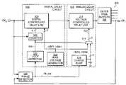
- FIG. 3is a block diagram of a wide frequency range delay locked loop (DLL) 300 according to the principles of the present invention.
- the wide frequency range DLL 300has two domains of operation: a digital domain which includes a digital delay circuit 302 and an analog domain which includes an analog delay circuit 304 .
- the wide frequency range DLL 300combines the two techniques to provide high accuracy, good stability and a fast lock time over a wide frequency range.
- the digital delay circuit 302is responsible for coarse phase adjustment during initialization and the analog delay circuit 304 is responsible for fine phase adjustment during normal operation, after coarse phase adjustment is completed by the digital delay circuit 302 .
- the digital delay circuit 302operates within the wide delay range and brings the delay locked loop 300 to a stable operation point during power-up initialization.
- the analog delay circuit 304operates within a small delay range of the stable operation point within the wide delay range and maintains the delay locked loop at the stable operation point while the digital delay circuit 302 is held at a fixed delay.
- the overall delay provided by the DLLincludes a digitally controlled delay line (DCDL) 306 having a set of delay elements, each having a fixed delay and a voltage controlled delay line (VCDL) 312 .
- DCDLdigitally controlled delay line
- VCDLvoltage controlled delay line
- the combination of the DCDL delay provided by the DCDL 306 and the VCDL delay provided by the VCDL 312provides an accurate delay. Only one of the domains can vary the DLL delay at any time.
- the digital delay circuit 302varies the DCDL 306 (coarse delay). After coarse phase adjustment is complete (lock is reached), the DCDL delay is held at a fixed number of DCDL delay elements (frozen) and the analog delay circuit 304 varies the DLL delay to provide fine phase adjustment by varying the VCDL delay.
- the digital delay circuit 302operates within the wide delay range to bring the DLL 300 to the operation point (lock) quickly to provide a short lock time.
- a lock detector 310 in the digital delay circuit 302detects when the digital delay circuit 302 has brought the DLL delay to the stable operation point and enables control of the DLL delay to be switched to the analog delay circuit 304 .
- a phase detector 320detects the phase difference between the external clock signal CKE and the internal clock signal CKI.
- the phase detector 320can be any phase detector well known to those skilled in the art.
- the phase detector 320( FIG. 3 ) includes a D-type flip-flop with CKI connected to the clock input and CKE connected to the D-input. The rising edge of CKI latches the state of CKE at the output (Ph_det) of the D-type flip-flop.
- the analog delay circuit 304includes a multiplexor 314 , a VCDL 312 and a charge pump 316 .
- the VCDL 312is a chain of differential-input-differential-output stages (delay elements) each controlled by two bias voltages VBP, VBN which can be provided by two different sources under control of the multiplexor 314 as will be described in further detail later.
- a single signalis used to designate the two bias voltages from each source, i.e. VBP 2 , VBN 2 and VBP 1 , VBN 1 .
- the multiplexor 314selects the source of the VCDL bias voltages 322 to the VCDL 312 .
- the VCDL bias voltages 322can be either of bias voltage pair VBP 1 , VBN 1 provided by bias voltage generator 318 or a variable bias voltage pair VBP 2 , VBN 2 provided by charge pump 316 .
- the differential bias voltage VBP 1 , VBN 1 pairis provided to the VCDL bias voltage 322 through multiplexor 314 .
- the digital delay circuit 302selects the DCDL delay
- the VCDL bias voltage 322provides a constant VCDL delay. That delay may be in the middle of the full delay range of the VCDL to enable fine tuning in both positive and negative directions as discussed below.
- the code stored in a counter 308is initialized to zero, which corresponds to the minimum delay; that is, the minimum number of delay elements in the DCDL 306 that are enabled.
- the lock detector 310allows the DCDL 306 to increase the DCDL delay by adding delay elements as the counter 318 is incremented until the nearest rising edge of the internal clock signal CKI is aligned with the rising edge of the external clock signal CKE.
- the counter 308is incremented by the external clock signal CKE until lock is reached (the clocks edges are aligned).
- the counter 308is an up-counter which increments on each rising edge of the external clock signal CKE while enabled by the SW signal from the lock detector 310 .
- Delay elements in the DCDL 306are added to the DCDL delay line based on the c-bit count value output by the counter 308 to enable the minimum number of DCDL delay elements necessary dependent on the bias voltage pair VBP 1 , VBN 1 .
- the SW signal output by the lock detector 310disables any further incrementing of the counter 308 .
- the VCDL bias voltage 322is provided by bias voltage pair VBP 2 , VBN 2 , the output of charge pump 316 , through multiplexor 314 .
- the charge pump 316can be any charge pump well known to those skilled in the art.
- the overall delay lineis minimum length to minimize noise.
- the enabled delay elementsprovide coarse phase adjustment in the delay locked loop. Once lock is reached, the digital delay circuit 302 is held at a fixed delay by disabling further incrementing of the counter 308 . Only the VCDL portion of the DLL delay line can be varied by the analog delay circuit 304 to provide fine phase adjustment in the delay locked loop.
- the analog delay circuit 304fine tunes the DLL delay to compensate for all drifts and condition changes during normal operation of the DLL, to keep the external and internal clock signal edges aligned, by varying the VCDL delay, which is added to the fixed delay provided by the DCDL.
- the analog controlled delay line 310varies the VCDL delay up or down by varying the bias voltage to the VCDL delay elements 402 based on detected phase difference between the clocks.
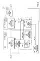
- FIG. 4illustrates in further detail delay elements in the DCDL and the VCDL.
- the digitally controlled delay line (DCDL)includes a chain of DCDL delay elements 400 and the voltage controlled delay line (VCDL) includes a chain of VCDL delay elements 402 .
- the delay of each DCDL cell 400is fixed by permanently connecting the bias voltage for each DCDL cell 400 to a fixed bias voltage pair VBP 1 , VBN 1 .
- the fixed bias voltage pair VBP 1 , VBN 1is provided by a bias voltage generator 318 ( FIG. 3 ) which can be any type of voltage stabilizing device, for example, a band-gap reference and need not correspond to the VCDL bias voltage 322 initially applied to the VCDL as will be discussed in further detail below.
- FIG. 5is a schematic of one embodiment of any one of the delay elements shown in FIG. 4 .
- the delay element 400includes a source-coupled pair of NMOS devices T 1 , T 2 with symmetric loads 500 , 502 .
- the differential input clock signal CKEI ⁇ , CKEI+is coupled to the respective gates of NMOS devices T 1 , T 2 with CKEI+ coupled to the gate of NMOS device T 1 and CKEI ⁇ coupled to the gate of NMOS device T 2 .
- the differential output clock signal CKEO ⁇ , CKEO+is coupled to the respective drains of NMOS devices T 1 , T 2 .
- the sources of NMOS devices T 1 and T 2are coupled and are also coupled to the drain of NMOS current source T 3 .
- NMOS current source T 3compensates for drain and substrate voltage variations.
- Symmetric load 500includes a diode-connected PMOS device T 4 connected in parallel with a biased PMOS device T 5 .
- Symmetric load 502includes a diode-connected PMOS device T 7 connected in parallel with a biased PMOS device T 6 .
- the effective resistance of the symmetric loads 500 , 502changes with changes in the bias voltage VBP 1 resulting in a corresponding change in delay through the delay stage from the differential clock input to the differential clock output.
- the DLL delayincludes only the fixed delay provided by demultiplexor 404 , multiplexor 408 and the VCDL delay elements 402 in the VCDL connected to the fixed bias voltage pair VBP 1 , VBN 1 .
- the VCDL delay provided by VCDLis dependent on the fixed bias voltage pair VBP 1 , VBN 1 .
- the DCDL delay elements 400 and the VCDL delay elements 402are the same delay element with voltage controlled delay.
- the DCDL delay element 400can differ from the VCDL delay element 402 , which is described and illustrated in FIG. 5 .
- the DCDL delayis varied by increasing the number of DCDL delay elements 400 with each DCDL delay element 400 having the same delay set by the fixed bias voltage pair VBP 1 , VBN 1 .
- the same fixed bias voltage pair VBP 1 , VBN 1is coupled to the DCDL delay elements 400 and the VCDL elements 402 .
- the fixed bias voltage coupled to the VCDL delay elements 402 and the DCDL delay elements 400can be different; for example, a first bias voltage VBP 1 may be set to 0.3VDD coupled to the DCDL and a second bias voltage VBP 2 may be set to 0.5VDD coupled to the VCDL.
- the VCDL delayis initially fixed with each of the three VCDL delay elements 402 numbered 1 - 3 coupled to the fixed bias voltage pair VBP 1 , VBN 1 , but the VCDL delay varies with changes in the VCDL bias voltage pair 322 VBP 2 , VBN 2 during normal operation.
- the number of delay elements enabled in the DCDL 306is dependent on the c-bit count 406 output by the counter 308 .
- the c-bit count 406is coupled to multiplexor select logic 430 which provides an m-bit multiplexor select signal, with one of each of the m-bits coupled to each multiplexor in the DCDL 306 and a d-bit de-multiplexor select signal 432 coupled to the de-multiplexor 404 .
- the d-bit de-multiplexor select signal 406is coupled to the de-multiplexor 404 to select the output of the de-multiplexor 404 through which the external clock is output to the DCDL 306 .
- the multiplexor select logic 430is a decoder which decodes the c-bit count to provide the m-bit multiplexor select signal.
- m and dare both 7 and c is 3.
- m and dcan be different.
- the multiplexor select logic 430decodes a three bit count 406 to select one of the seven multiplexors through which to provide the external clock to the respective delay element as shown in Table 1 below.
- the Most Significant Bit (MSB) of the seven bit multiplexor select signalcorresponds to the select signal for multiplexor 420 and the Least Significant Bit (LSB) of the seven bit multiplexor signal corresponds to the select signal for multiplexor 408 .
- MSBMost Significant Bit
- LSBLeast Significant Bit
- the multiplexor select logiccan be implemented as a shift register clocked by the external clock and enabled by the SW signal.
- the external clock signal CKEis delayed through DCDL delay elements enabled dependent on the c-bit count output by counter 308 .
- Control of the DLL delayis switched to the VCDL 312 by switching the bias voltage provided to the VCDL from the bias voltage pair VBP 1 , VBN 1 to the bias voltage pair VBP 2 , VBN 2 through the multiplexor 314 ( FIG. 3 ).
- the DLL delayincludes minimum delay provided by the enabled DCDL delay elements 400 in the DCDL 306 and additional delay provided by the VCDL 312 to provide an accurate DLL delay.
- the stability of the DLLis increased by using the digital domain to cover a wide delay range to obtain a minimum delay, then freezing the digital domain to allow the analog domain to operate within a small delay range to provide fine phase adjustment in the delay locked loop by controlling the DLL delay.
- the bias voltage coupled to the VCDL bias voltage 322is set so that the VCDL does not control the overall DLL delay until after a locked condition is detected by the digital domain. Before locked condition, the VCDL merely provides a constant delay independent of the phase difference between the clocks.
- the counter 308is implemented as a ripple counter. Initially the counter 308 is reset to 0.
- the de-multiplexor 404steers the external clock CKE to delay elements dependent on the d-bit de-multiplexor select signal 432 output by the multiplexor select logic 430 . With the output of the counter 308 set to ‘0’ and the de-multiplexor select signal 432 set to ‘1111110’, CKE is steered through output 422 of de-multiplexor 404 coupled to multiplexor 408 and no delay DCDL elements 400 are enabled.
- the clock signal CKEis steered through the output 424 of the de-multiplexor 404 by the counter output set to ‘1’ to enable DCDL delay stage labeled 4 .
- Multiplexor 410is enabled to allow CKE to be steered through to DCDL delay stage 400 as the m-bit multiplexor select signal output by multiplexor select logic 430 steers delayed CKE through multiplexor 408 to the VCDL.
- the embodiment of the de-multiplexor 404can be implemented with a plurality of PMOS transistors each enabled by an active logic low signal with all other signals held at logic high, as illustrated in Table 1. Alternately, NMOS transistors or full CMOS pass gates could be utilized to implement the de-multiplexor 404 .
- All six DCDL delay stagesare enabled when the counter output is set to six, and CKE is directed through de-multiplexor output 426 through multiplexors 420 , 418 , 416 , 414 , 412 , 410 , 408 and delay elements labeled 9 - 4 .
- the DCDL lineis frozen when the counter 308 is disabled by the SW signal set to logic low.
- FIG. 6is a graph illustrating the non-linear control voltage characteristic for the narrow delay range of the VCDL 312 in the DLL 300 shown in FIG. 3 .
- the digital domainprovides the minimum delay to bring the operating range of the DLL 300 to point B.
- the analog domainoperates within a narrow delay range 600 from point B-High to point B-Low.
- This delay rangeis much smaller than the wide delay range supported by the DLL, but may be controlled by the same large voltage range as applied in the pure analog case of FIG. 2 .
- the small delay range controlled by a large voltage rangeensures the stability of the analog domain during normal operation of the DLL.
- the analog delay circuit 304operates within the delay range 85 ns to 80 ns over voltage range 200 mV to 800 mV to provide fine phase adjustment for the delay locked loop. In contrast to the wide delay range over the same voltage range shown in FIG. 2 , a small variation in control voltage ( ⁇ V) does not substantially affect the delay.
- FIG. 7is a schematic of an embodiment of the lock detector 310 and the multiplexor 314 shown in FIG. 3 .
- the lock detector 310includes two SR flip-flops 700 , 702 , AND gate 706 and inverter 704 .
- SR flip-flop 700detects when the internal clock signal CKI is within a phase detection window.
- SR flip-flop 702detects when the internal clock signal CKI is in phase with the external clock signal CKE. Once the internal clock signal CKI is in phase with the external clock signal CKE the SW signal is set to logic ‘0’ to disable further changes to the DCDL delay.
- the lock detector output SWis held at logic ‘0’ prior to lock being reached and set to logic ‘1’ after lock is reached.
- the logic ‘0’ on the SW signalcouples the fixed bias voltage through multiplexor 314 to provide the VCDL bias voltage pair 322 .
- the logic ‘1’ on SWcouples the variable bias voltage pair VBPN 2 , VBPN 2 through multiplexor 314 to provide the VCDL bias voltage pair 322 , to allow the VCDL 312 to fine tune the overall delay.
- the reset signal coupled to the R-input of the SR flip-flop 700 and the SR flip-flop 702is set to logic ‘1’. Both flip-flops 700 , 702 are reset with the respective Q outputs (LC 1 , SW) set to logic ‘0’.
- the SR flip-flops 700 , 702remain in a reset state with logic ‘0’ on the respective Q outputs until the phase detector 320 detects that the phase difference between clock signals CKE, CKI are in the phase detection window.
- the phase differenceis within the phase detection window while the rising edge of the internal clock signal CKI occurs after the falling edge of the external clock signal CKE.
- the output of the phase detector (Ph_det)changes to logic ‘0’.
- Ph_detchanges the S-input of SR flip flop 700 to logic ‘1’ through inverter 704 which sets SR flip-flop 700 (i.e. the Q output changes to logic ‘1’).
- the delay provided by the DCDL 306continues to increase further delaying the rising edge of the internal clock signal until the internal clock signal and the external clock signals are in phase.
- SR flip-flop 702is set on the next rising edge of Ph-det which occurs when the rising edge of CKE is detected after the rising edge of CKI.
- the Q output of SR flip-flop 702is set to logic ‘1’ indicating that coarse phase adjustment is provided by the digital delay circuit.
- the lock detector 310remains in a locked state with SW set to logic ‘1’ until the system is reset. While in the locked state, the digital domain no longer controls the delay because, while SW is set to logic ‘1’, the code stored in the counter 308 is frozen to freeze the DCDL delay.
- FIGS. 8A-Care timing diagrams illustrating the relationship of the phase detector output (Ph-det) to the phase difference between the clocks.
- the phase detector 320FIG. 3
- the phase detector 320detects that the internal clock rising edge occurs after the external clock rising edge.
- the rising edge of CKIlatches a ‘1’ on the Ph_det output of the D-type flip-flop.
- the CKE rising edgecontinues to increment the code to add additional delay to the DCDL.
- the phase detectordetects that the CKI rising edge is now after the falling edge of CKE, i.e. the internal clock rising edge is within a phase detection window.
- the rising edge of CKIlatches a ‘0’ on the Ph_det output of the D-type flip-flop.
- the CKE rising edgeincrements the code to add further delay elements 400 to the DCDL.
- the phase detectordetects the lock condition when the CKI rising edge moves after the CKE rising edge.
- the rising edge of CKIlatches a ‘1’ on the Ph_det output of the D-type flip-flop.
- FIG. 9is a timing diagram illustrating signals in the schematic shown in FIG. 7 .
- the timing diagramshows the state of signals in the schematic when the system is reset, upon detecting that the phase detection window has been reached and upon detecting the lock condition (when the clock edges of CKE and CKI are aligned).
- FIG. 9is described in conjunction with FIG. 3 and FIG. 7 .
- the systemis reset and the reset signal switches to logic ‘1’.
- the reset signalis coupled to the R-inputs of flip-flops 700 , 702 to reset the flip-flops.
- the Ph_det signalis reset to logic ‘1’.
- the Q outputs (LC 1 , SW) of both flip-flopsare reset to ‘0’.
- the internal clock signal CKIhas the same frequency as the external clock signal CKE but there is an initial phase difference due to the delay of CKE through the clock tree buffers 328 .
- the reset signalchanges to logic ‘0’.
- Initially delayis added to CKE through the DCDL and no delay is added through the VCDL.
- the rising edge of CKIoccurs later than the rising edge of CKE due to the delay through the clock tree buffers 328 ( FIG. 3 ) and the delay through the DCDL.
- the SW signal set to logic ‘0’allows CKE to increment the code stored in the counter 308 ( FIG. 3 ).
- the delay between CKE and CKIincreases until the phase detection window is reached.
- the phase detector 320detects that the phase detection window has been entered.
- the Ph_det signal output from the phase detectorchanges state from logic ‘1’ to logic ‘0’ indicating that the phase detector 320 has detected a rising edge of CKI signal after a falling edge of CKE.
- SR flip-flop 600is set, and LC 1 at the Q output is set to ‘1’.
- the phase difference between CKE and CKIdecreases as the DCDL delay is increased.
- the phase detector 320( FIG. 3 ) detects that the sufficient delay has been added by the DCDL such that the rising edge of CKI occurs after the rising edge of CKE.
- the Ph-det output of the phase detector 320changes to back to logic ‘1’.
- LC 2 at the output of AND gate 706changes to logic ‘1’, the SR flip-flop 702 is set and the Q output (SW) changes to logic ‘1’. Further changes on the Ph-det signal do not affect the state of LC 1 and SW.
- the SW signal set to ‘1’disables further incrementing of the counter 308 .
- the delay adjustment of the clock path to compensate for drifts and condition changescovers a narrow range of the wide delay range.
- the DCDLenables delay elements to provide coarse phase adjustment in the delay locked loop.
- the DLL delayis varied by the VCDL inside a smaller delay range to provide fine phase adjustment in the delay locked loop. Monitoring the smaller delay range during normal operation provides more stability and reduces the controlling voltage node sensitivity.
- the systemresets to initial conditions and the DCDL is reactivated to bring the external and internal clocks within the phase detection window range.
- the inventionhas been described for an embodiment having a single fixed bias voltage level.
- more than one fixed bias voltage level, or more than one fixed bias voltage pair levelscan be used to provide a more compact DLL that is less noise sensitive.
- Thisallows the wide delay range to be modified in order to reduce the number of DCDL delay elements by selecting a fixed bias voltage level dependent on the frequency of the external clock. Reducing the number of DCDL delay elements, reduces sensitivity to noise. For example, in one embodiment, with a fixed bias voltage of 0.6VDD, fifteen DCDL delay elements are required to provide the DCDL delay. When the fixed bias voltage is 0.7VDD, only eight DCDL delay elements are required to provide the DCDL delay. However, changing the delay range may result in the delay range covering an unstable region, for example, at point C in the graph shown in FIG. 2 .
- the inventioncan be used in integrated circuits requiring high accuracy of input/output data synchronization, for example, in memory, microprocessor and Application Specific Integrated Circuits (ASICs).
- ASICsApplication Specific Integrated Circuits
Landscapes
- Stabilization Of Oscillater, Synchronisation, Frequency Synthesizers (AREA)
- Pulse Circuits (AREA)
- Dram (AREA)
- Saccharide Compounds (AREA)
- Pharmaceuticals Containing Other Organic And Inorganic Compounds (AREA)
Abstract
Description
| TABLE 1 | ||
| Counter output | Multiplexor select | De-multiplexor select |
| count[2:0] | mux_en[6:0] | demux_sel[6:0] |
| 000 | 1111110 | 1111110 |
| 001 | 1111101 | 1111101 |
| 010 | 1111011 | 1111011 |
| 011 | 1110111 | 1110111 |
| 100 | 1101111 | 1101111 |
| 101 | 1011111 | 1011111 |
| 110 | 0111111 | 0111111 |
Claims (17)
Priority Applications (21)
| Application Number | Priority Date | Filing Date | Title |
|---|---|---|---|
| US10/335,535US7336752B2 (en) | 2002-12-31 | 2002-12-31 | Wide frequency range delay locked loop |
| DE60334032TDE60334032D1 (en) | 2002-12-31 | 2003-12-29 | ANALOG / DIGITAL DLL |
| ES03785447TES2349123T3 (en) | 2002-12-31 | 2003-12-29 | CLOSED LOOP OF ANALOG / NUMERICAL DELAY. |
| CN201210007453.8ACN102522986B (en) | 2002-12-31 | 2003-12-29 | Analog / digital delay locked loop |
| AU2003294604AAU2003294604A1 (en) | 2002-12-31 | 2003-12-29 | Analogue/digital delay locked loop |
| EP10183259AEP2264902A1 (en) | 2002-12-31 | 2003-12-29 | Analogue/digital delay locked loop |
| CN2003801078732ACN1732623B (en) | 2002-12-31 | 2003-12-29 | Analog/Digital Delay Locked Loop |
| KR1020107013836AKR101051875B1 (en) | 2002-12-31 | 2003-12-29 | Analogue/digital delay locked loop |
| AT03785447TATE480049T1 (en) | 2002-12-31 | 2003-12-29 | ANALOG/DIGITAL DLL |
| KR1020057012303AKR101106369B1 (en) | 2002-12-31 | 2003-12-29 | Analog / Digital Delay Lock Loop |
| EP03785447AEP1588489B1 (en) | 2002-12-31 | 2003-12-29 | Analogue/digital delay locked loop |
| EP10171395AEP2251980B1 (en) | 2002-12-31 | 2003-12-29 | Analogue/digital delay locked loop |
| ES10171395TES2385786T3 (en) | 2002-12-31 | 2003-12-29 | Closed loop analog / digital delay |
| PCT/CA2003/002040WO2004059846A1 (en) | 2002-12-31 | 2003-12-29 | Analogue/digital delay locked loop |
| US11/999,162US8000430B2 (en) | 2002-12-31 | 2007-12-04 | Wide frequency range delay locked loop |
| US13/186,104US8213561B2 (en) | 2002-12-31 | 2011-07-19 | Wide frequency range delay locked loop |
| US13/523,406US8411812B2 (en) | 2002-12-31 | 2012-06-14 | Wide frequency range delay locked loop |
| HK12110872.8AHK1170079B (en) | 2002-12-31 | 2012-10-30 | Analogue/digital delay locked loop |
| US13/850,500US8599984B2 (en) | 2002-12-31 | 2013-03-26 | Wide frequency range delay locked loop |
| US14/092,788US20140084977A1 (en) | 2002-12-31 | 2013-11-27 | Wide Frequency Range Delay Locked Loop |
| US15/479,691US10122369B2 (en) | 2002-12-31 | 2017-04-05 | Wide frequency range delay locked loop |
Applications Claiming Priority (1)
| Application Number | Priority Date | Filing Date | Title |
|---|---|---|---|
| US10/335,535US7336752B2 (en) | 2002-12-31 | 2002-12-31 | Wide frequency range delay locked loop |
Related Child Applications (1)
| Application Number | Title | Priority Date | Filing Date |
|---|---|---|---|
| US11/999,162ContinuationUS8000430B2 (en) | 2002-12-31 | 2007-12-04 | Wide frequency range delay locked loop |
Publications (2)
| Publication Number | Publication Date |
|---|---|
| US20040125905A1 US20040125905A1 (en) | 2004-07-01 |
| US7336752B2true US7336752B2 (en) | 2008-02-26 |
Family
ID=32655375
Family Applications (7)
| Application Number | Title | Priority Date | Filing Date |
|---|---|---|---|
| US10/335,535Expired - LifetimeUS7336752B2 (en) | 2002-12-31 | 2002-12-31 | Wide frequency range delay locked loop |
| US11/999,162Expired - Fee RelatedUS8000430B2 (en) | 2002-12-31 | 2007-12-04 | Wide frequency range delay locked loop |
| US13/186,104Expired - Fee RelatedUS8213561B2 (en) | 2002-12-31 | 2011-07-19 | Wide frequency range delay locked loop |
| US13/523,406Expired - Fee RelatedUS8411812B2 (en) | 2002-12-31 | 2012-06-14 | Wide frequency range delay locked loop |
| US13/850,500Expired - LifetimeUS8599984B2 (en) | 2002-12-31 | 2013-03-26 | Wide frequency range delay locked loop |
| US14/092,788AbandonedUS20140084977A1 (en) | 2002-12-31 | 2013-11-27 | Wide Frequency Range Delay Locked Loop |
| US15/479,691Expired - LifetimeUS10122369B2 (en) | 2002-12-31 | 2017-04-05 | Wide frequency range delay locked loop |
Family Applications After (6)
| Application Number | Title | Priority Date | Filing Date |
|---|---|---|---|
| US11/999,162Expired - Fee RelatedUS8000430B2 (en) | 2002-12-31 | 2007-12-04 | Wide frequency range delay locked loop |
| US13/186,104Expired - Fee RelatedUS8213561B2 (en) | 2002-12-31 | 2011-07-19 | Wide frequency range delay locked loop |
| US13/523,406Expired - Fee RelatedUS8411812B2 (en) | 2002-12-31 | 2012-06-14 | Wide frequency range delay locked loop |
| US13/850,500Expired - LifetimeUS8599984B2 (en) | 2002-12-31 | 2013-03-26 | Wide frequency range delay locked loop |
| US14/092,788AbandonedUS20140084977A1 (en) | 2002-12-31 | 2013-11-27 | Wide Frequency Range Delay Locked Loop |
| US15/479,691Expired - LifetimeUS10122369B2 (en) | 2002-12-31 | 2017-04-05 | Wide frequency range delay locked loop |
Country Status (9)
| Country | Link |
|---|---|
| US (7) | US7336752B2 (en) |
| EP (3) | EP2264902A1 (en) |
| KR (2) | KR101051875B1 (en) |
| CN (2) | CN1732623B (en) |
| AT (1) | ATE480049T1 (en) |
| AU (1) | AU2003294604A1 (en) |
| DE (1) | DE60334032D1 (en) |
| ES (2) | ES2349123T3 (en) |
| WO (1) | WO2004059846A1 (en) |
Cited By (43)
| Publication number | Priority date | Publication date | Assignee | Title |
|---|---|---|---|---|
| US20060114039A1 (en)* | 2004-11-30 | 2006-06-01 | Freyman Ronald L | Voltage controlled delay loop and method with injection point control |
| US20070002675A1 (en)* | 2005-06-30 | 2007-01-04 | Koo Cheul H | Synchronous memory device with output driver controller |
| US20080088349A1 (en)* | 2005-02-28 | 2008-04-17 | Hynix Semiconductor Inc. | Delay locked loop circuit in semiconductor device and its control method |
| US20080089459A1 (en)* | 2002-12-31 | 2008-04-17 | Mosaid Technologies, Inc. | Wide frequency range delay locked loop |
| US20080100356A1 (en)* | 2006-10-25 | 2008-05-01 | Dong-Jin Lee | Delay locked loop circuit |
| US20080122502A1 (en)* | 2006-08-24 | 2008-05-29 | Hynix Semiconductor Inc. | Delay locked loop circuit for preventing malfunction caused by change of power supply voltage |
| US20080232178A1 (en)* | 2007-03-20 | 2008-09-25 | Nec Corporation | Apparatus and method for controlling delay of signal |
| US20080231333A1 (en)* | 2007-03-20 | 2008-09-25 | Hsien-Sheng Huang | Spread Spectrum Clock Generator |
| US20080238507A1 (en)* | 2007-03-30 | 2008-10-02 | Hynix Semiconductor Inc. | Semiconductor memory device |
| US20090045858A1 (en)* | 2005-09-29 | 2009-02-19 | Hynix Semiconductor Inc. | Delay locked loop circuit |
| US20090115486A1 (en)* | 2007-11-02 | 2009-05-07 | Hynix Semiconductor Inc. | Apparatus and method for generating multi-phase clocks |
| US20090189658A1 (en)* | 2008-01-25 | 2009-07-30 | Elpida Memory, Inc. | DLL circuit, semiconductor device using the same, and method for controlling DLL circuit |
| US20090243661A1 (en)* | 2008-03-31 | 2009-10-01 | Bin Xue | System and method to detect order and linearity of signals |
| US20100123495A1 (en)* | 2008-11-17 | 2010-05-20 | Elpida Memory, Inc. | DLL circuit and semiconductor device having the same |
| US20100164568A1 (en)* | 2008-12-26 | 2010-07-01 | Hynix Semiconductor Inc. | Low power variable delay circuit |
| US20100199117A1 (en)* | 2006-12-19 | 2010-08-05 | Micron Technology, Inc. | Timing synchronization circuit with loop counter |
| US20100201413A1 (en)* | 2009-02-12 | 2010-08-12 | Elpida Memory, Inc. | Clock control circuit and semiconductor device including the same |
| US20100213992A1 (en)* | 2009-02-20 | 2010-08-26 | Samsung Electronics Co., Ltd. | Delay locked loop circuit and operation method thereof |
| US20100253404A1 (en)* | 2009-04-01 | 2010-10-07 | Yantao Ma | Clock jitter compensated clock circuits and methods for generating jitter compensated clock signals |
| US20110063004A1 (en)* | 2009-09-14 | 2011-03-17 | Sunplus Technology Co., Ltd. | Frequency synthesis system with self-calibrated loop stability and bandwidth |
| US20110298512A1 (en)* | 2007-03-15 | 2011-12-08 | Micron Technology, Inc. | Circuit, system and method for controlling read latency |
| US8638144B1 (en)* | 2009-12-30 | 2014-01-28 | Gsi Technology, Inc. | Systems and methods involving phase detection with adaptive locking/detection features |
| US20140266336A1 (en)* | 2013-03-15 | 2014-09-18 | Silicon Laboratories Inc. | Clock signal timing-based noise suppression |
| US8913448B2 (en) | 2012-10-25 | 2014-12-16 | Micron Technology, Inc. | Apparatuses and methods for capturing data in a memory |
| US8984320B2 (en) | 2011-03-29 | 2015-03-17 | Micron Technology, Inc. | Command paths, apparatuses and methods for providing a command to a data block |
| US8994424B2 (en)* | 2013-03-12 | 2015-03-31 | International Business Machines Corporation | Distributing multiplexing logic to remove multiplexor latency on the output path for variable clock cycle, delayed signals |
| US9001594B2 (en) | 2012-07-06 | 2015-04-07 | Micron Technology, Inc. | Apparatuses and methods for adjusting a path delay of a command path |
| US9000817B2 (en) | 2012-02-01 | 2015-04-07 | Micron Technology, Inc. | Apparatuses and methods for altering a forward path delay of a signal path |
| US9054675B2 (en) | 2012-06-22 | 2015-06-09 | Micron Technology, Inc. | Apparatuses and methods for adjusting a minimum forward path delay of a signal path |
| US9166579B2 (en) | 2012-06-01 | 2015-10-20 | Micron Technology, Inc. | Methods and apparatuses for shifting data signals to match command signal delay |
| US9329623B2 (en) | 2012-08-22 | 2016-05-03 | Micron Technology, Inc. | Apparatuses, integrated circuits, and methods for synchronizing data signals with a command signal |
| US9356611B1 (en) | 2009-12-30 | 2016-05-31 | Gsi Technology, Inc. | Systems and methods involving phase detection with adaptive locking/detection features |
| US9417657B2 (en)* | 2014-10-02 | 2016-08-16 | Nxp B.V. | Timing control with body-bias |
| US9438255B1 (en)* | 2015-07-31 | 2016-09-06 | Inphi Corporation | High frequency delay lock loop systems |
| US9508417B2 (en) | 2014-02-20 | 2016-11-29 | Micron Technology, Inc. | Methods and apparatuses for controlling timing paths and latency based on a loop delay |
| US9530473B2 (en) | 2014-05-22 | 2016-12-27 | Micron Technology, Inc. | Apparatuses and methods for timing provision of a command to input circuitry |
| US9531363B2 (en) | 2015-04-28 | 2016-12-27 | Micron Technology, Inc. | Methods and apparatuses including command latency control circuit |
| US9601170B1 (en) | 2016-04-26 | 2017-03-21 | Micron Technology, Inc. | Apparatuses and methods for adjusting a delay of a command signal path |
| US9813067B2 (en) | 2015-06-10 | 2017-11-07 | Micron Technology, Inc. | Clock signal and supply voltage variation tracking |
| US9865317B2 (en) | 2016-04-26 | 2018-01-09 | Micron Technology, Inc. | Methods and apparatuses including command delay adjustment circuit |
| US9997220B2 (en) | 2016-08-22 | 2018-06-12 | Micron Technology, Inc. | Apparatuses and methods for adjusting delay of command signal path |
| US10224938B2 (en) | 2017-07-26 | 2019-03-05 | Micron Technology, Inc. | Apparatuses and methods for indirectly detecting phase variations |
| US11057040B2 (en)* | 2019-10-10 | 2021-07-06 | Samsung Electronics Co., Ltd. | Phase-locked loop circuit and clock generator including the same |
Families Citing this family (90)
| Publication number | Priority date | Publication date | Assignee | Title |
|---|---|---|---|---|
| JP2003324348A (en)* | 2002-04-30 | 2003-11-14 | Elpida Memory Inc | Dll circuit |
| US7149145B2 (en)* | 2004-07-19 | 2006-12-12 | Micron Technology, Inc. | Delay stage-interweaved analog DLL/PLL |
| US7138845B2 (en)* | 2004-07-22 | 2006-11-21 | Micron Technology, Inc. | Method and apparatus to set a tuning range for an analog delay |
| US7126393B2 (en)* | 2004-08-20 | 2006-10-24 | Micron Technology, Inc. | Delay circuit with reset-based forward path static delay |
| KR100667154B1 (en)* | 2004-10-26 | 2007-01-12 | 한국전자통신연구원 | Frequency lock detector |
| US7190201B2 (en) | 2005-02-03 | 2007-03-13 | Mosaid Technologies, Inc. | Method and apparatus for initializing a delay locked loop |
| US7425858B1 (en) | 2005-09-16 | 2008-09-16 | Advanced Micro Devices, Inc. | Delay line periodically operable in a closed loop |
| US7271634B1 (en)* | 2005-09-16 | 2007-09-18 | Advanced Micro Devices, Inc. | Delay-locked loop having a plurality of lock modes |
| KR100743493B1 (en)* | 2006-02-21 | 2007-07-30 | 삼성전자주식회사 | Adaptive Delay Locked Loop |
| US20070216455A1 (en)* | 2006-03-17 | 2007-09-20 | M/A-Com, Inc. | Partial cascode delay locked loop architecture |
| US20070230646A1 (en)* | 2006-03-28 | 2007-10-04 | Talbot Gerald R | Phase recovery from forward clock |
| US8570881B2 (en)* | 2006-03-28 | 2013-10-29 | Advanced Micro Devices, Inc. | Transmitter voltage and receiver time margining |
| US7817761B2 (en)* | 2007-06-01 | 2010-10-19 | Advanced Micro Devices, Inc. | Test techniques for a delay-locked loop receiver interface |
| US8045662B2 (en)* | 2007-06-22 | 2011-10-25 | Texas Instruments Incorporated | Binary ripple counter sampling with adjustable delays |
| US7885365B2 (en)* | 2007-08-31 | 2011-02-08 | International Business Machines Corporation | Low-power, low-area high-speed receiver architecture |
| KR100974211B1 (en)* | 2008-02-14 | 2010-08-06 | 주식회사 하이닉스반도체 | Locking State Detector and DLL Circuit Containing It |
| US8032778B2 (en)* | 2008-03-19 | 2011-10-04 | Micron Technology, Inc. | Clock distribution apparatus, systems, and methods |
| JP2009278528A (en)* | 2008-05-16 | 2009-11-26 | Elpida Memory Inc | Dll circuit, and semiconductor device |
| US7876137B2 (en)* | 2008-11-20 | 2011-01-25 | Promos Technologies Pte.Ltd. | Configurable architecture hybrid analog/digital delay locked loop (DLL) and technique with fast open loop digital locking for integrated circuit devices |
| KR101012678B1 (en)* | 2009-02-04 | 2011-02-09 | 연세대학교 산학협력단 | Delay Synchronous Loops and Electronic Devices Comprising the Same |
| EP2242178A1 (en)* | 2009-04-15 | 2010-10-20 | Nxp B.V. | Digital phase shifting for imparting a target delay on an input signal to generate an output signal |
| JP5314533B2 (en)* | 2009-08-19 | 2013-10-16 | 株式会社アドバンテスト | Driver circuit and test apparatus using the same |
| US8638138B2 (en)* | 2009-09-14 | 2014-01-28 | Achronix Semiconductor Corporation | Hierarchical global clock tree |
| US8786334B2 (en)* | 2010-07-30 | 2014-07-22 | Samsung Electronics Co., Ltd. | Lock detection circuit and phase-locked loop circuit including the same |
| US8368444B2 (en)* | 2010-10-11 | 2013-02-05 | Apple Inc. | Delay locked loop including a mechanism for reducing lock time |
| KR101811020B1 (en)* | 2010-10-26 | 2017-12-20 | 마벨 월드 트레이드 리미티드 | Pll dual edge lock detector |
| KR20120088136A (en)* | 2011-01-31 | 2012-08-08 | 에스케이하이닉스 주식회사 | Synchronization circuit |
| KR20120119343A (en)* | 2011-04-21 | 2012-10-31 | 에스케이하이닉스 주식회사 | Delay lock loop |
| US8598930B2 (en)* | 2011-08-23 | 2013-12-03 | Intel Corporation | Digital delay-locked loop with drift sensor |
| US9214945B2 (en)* | 2012-02-27 | 2015-12-15 | Realtek Semiconductor Corp. | Digital phase lock loop and method thereof |
| US8879139B2 (en) | 2012-04-24 | 2014-11-04 | Gentex Corporation | Display mirror assembly |
| US8977439B2 (en) | 2012-06-12 | 2015-03-10 | Genetex Corporation | Vehicle imaging system providing multi-stage aiming stability indication |
| EP2879912B1 (en) | 2012-08-02 | 2021-11-10 | Gentex Corporation | System and method for controlling exterior vehicle lights responsive to detection of a semi-truck |
| US8704568B1 (en)* | 2012-09-28 | 2014-04-22 | Analog Devices, Inc. | Sub-gate delay adjustment using digital locked-loop |
| KR20140112663A (en)* | 2013-03-14 | 2014-09-24 | 삼성전자주식회사 | Delay Locked Loop Circuit and Method of Control thereof |
| KR101735147B1 (en)* | 2013-05-22 | 2017-05-15 | 매그나칩 반도체 유한회사 | DLL circuit apparatus and method for locking thereof |
| JP2015012350A (en)* | 2013-06-27 | 2015-01-19 | マイクロン テクノロジー, インク. | Semiconductor device |
| JP2016534915A (en) | 2013-09-24 | 2016-11-10 | ジェンテックス コーポレイション | Display mirror assembly |
| CN103560786B (en)* | 2013-11-21 | 2017-07-28 | 东南大学 | A kind of digital successive approximation register formula quick lock in delay-locked loop |
| US9511715B2 (en) | 2014-01-31 | 2016-12-06 | Gentex Corporation | Backlighting assembly for display for reducing cross-hatching |
| US10705332B2 (en) | 2014-03-21 | 2020-07-07 | Gentex Corporation | Tri-modal display mirror assembly |
| KR101894262B1 (en) | 2014-04-01 | 2018-09-04 | 젠텍스 코포레이션 | Automatic display mirror assembly |
| US9571083B2 (en)* | 2014-08-22 | 2017-02-14 | Nokia Technologies Oy | All-digital delay-locked loop tuning method with randomized LSB-tuning |
| US9685961B2 (en) | 2014-09-17 | 2017-06-20 | Htc Corporation | High resolution timing device and radar detection system having the same |
| US9694751B2 (en) | 2014-09-19 | 2017-07-04 | Gentex Corporation | Rearview assembly |
| CN105490666B (en)* | 2014-09-19 | 2018-08-24 | 宏达国际电子股份有限公司 | High-resolution clock generation device and radar detection system |
| US9490821B2 (en)* | 2014-09-26 | 2016-11-08 | Apple Inc. | Glitch less delay circuit for real-time delay adjustments |
| JP6439367B2 (en)* | 2014-10-10 | 2018-12-19 | 富士通株式会社 | Delay circuit, phase synchronization circuit having delay circuit, and processor having phase synchronization circuit |
| WO2016073848A1 (en) | 2014-11-07 | 2016-05-12 | Gentex Corporation | Full display mirror actuator |
| US10071689B2 (en) | 2014-11-13 | 2018-09-11 | Gentex Corporation | Rearview mirror system with a display |
| CN105654986B (en)* | 2014-11-14 | 2020-02-07 | 群联电子股份有限公司 | Sampling circuit module, memory control circuit unit and data sampling method |
| US10131279B2 (en) | 2014-12-03 | 2018-11-20 | Gentex Corporation | Display mirror assembly with an RF shield bezel |
| USD746744S1 (en) | 2014-12-05 | 2016-01-05 | Gentex Corporation | Rearview device |
| US9744907B2 (en) | 2014-12-29 | 2017-08-29 | Gentex Corporation | Vehicle vision system having adjustable displayed field of view |
| US9720278B2 (en) | 2015-01-22 | 2017-08-01 | Gentex Corporation | Low cost optical film stack |
| JP2018513810A (en) | 2015-04-20 | 2018-05-31 | ジェンテックス コーポレイション | Rear view assembly with decoration |
| EP3297870B1 (en) | 2015-05-18 | 2020-02-05 | Gentex Corporation | Full display rearview device |
| CN107852153B (en)* | 2015-06-03 | 2021-04-27 | 马维尔亚洲私人有限公司 | Delay locked loop |
| US9407273B1 (en)* | 2015-06-04 | 2016-08-02 | Intel Corporation | Digital delay-locked loop (DLL) training |
| US9614533B2 (en) | 2015-06-19 | 2017-04-04 | Intel Corporation | Digital phase control with programmable tracking slope |
| WO2016209877A1 (en) | 2015-06-22 | 2016-12-29 | Gentex Corporation | System and method for processing streamed video images to correct for flicker of amplitude-modulated lights |
| US20190008859A1 (en) | 2015-08-21 | 2019-01-10 | Acerta Pharma B.V. | Therapeutic Combinations of a MEK Inhibitor and a BTK Inhibitor |
| CN108349436B (en) | 2015-10-30 | 2019-12-20 | 金泰克斯公司 | Rear-view device |
| WO2017075420A1 (en) | 2015-10-30 | 2017-05-04 | Gentex Corporation | Toggle paddle |
| USD798207S1 (en) | 2015-10-30 | 2017-09-26 | Gentex Corporation | Rearview mirror assembly |
| USD797627S1 (en) | 2015-10-30 | 2017-09-19 | Gentex Corporation | Rearview mirror device |
| USD800618S1 (en) | 2015-11-02 | 2017-10-24 | Gentex Corporation | Toggle paddle for a rear view device |
| CN105406858A (en)* | 2015-12-11 | 2016-03-16 | 合肥学院 | All-digital successive approximation register delay locking loop |
| CA3018325A1 (en)* | 2016-03-25 | 2017-09-28 | Walmart Apollo, Llc | Unmanned aircraft systems and methods of assembly |
| USD845851S1 (en) | 2016-03-31 | 2019-04-16 | Gentex Corporation | Rearview device |
| USD817238S1 (en) | 2016-04-29 | 2018-05-08 | Gentex Corporation | Rearview device |
| US10025138B2 (en) | 2016-06-06 | 2018-07-17 | Gentex Corporation | Illuminating display with light gathering structure |
| DE102016123459B3 (en)* | 2016-12-05 | 2018-05-30 | Infineon Technologies Ag | Apparatus, system and method for high frequency signal path calibration |
| USD809984S1 (en) | 2016-12-07 | 2018-02-13 | Gentex Corporation | Rearview assembly |
| US10110210B2 (en)* | 2016-12-16 | 2018-10-23 | Intel Corporation | Apparatus and method for strobe centering for source synchronous links |
| USD854473S1 (en) | 2016-12-16 | 2019-07-23 | Gentex Corporation | Rearview assembly |
| KR20190104990A (en) | 2016-12-30 | 2019-09-11 | 젠텍스 코포레이션 | Full display mirror with instant custom spotter view |
| EP3595931A4 (en) | 2017-03-17 | 2020-01-22 | Gentex Corporation | REVIEW REVERSE CAMERA WITH TWO |
| US10333532B2 (en)* | 2017-09-07 | 2019-06-25 | Micron Technology, Inc. | Apparatuses and methods for detecting a loop count in a delay-locked loop |
| CN107809238B (en)* | 2017-09-27 | 2021-03-23 | 珠海格力电器股份有限公司 | Phase-locked loop locking detection method based on MCU and MCU |
| KR102528561B1 (en)* | 2018-05-09 | 2023-05-04 | 삼성전자주식회사 | Apparatus and method for generating clock |
| KR20200075243A (en)* | 2018-12-18 | 2020-06-26 | 전자부품연구원 | High Resolution Delay with Multi-Stage Delay |
| US10706916B1 (en)* | 2019-04-03 | 2020-07-07 | Synopsys, Inc. | Method and apparatus for integrated level-shifter and memory clock |
| US11750201B2 (en) | 2019-09-06 | 2023-09-05 | SK Hynix Inc. | Delay line, a delay locked loop circuit and a semiconductor apparatus using the delay line and the delay locked loop circuit |
| US11206026B2 (en) | 2019-09-06 | 2021-12-21 | SK Hynix Inc. | Delay line, a delay locked loop circuit and a semiconductor apparatus using the delay line and the delay locked loop circuit |
| US11874694B2 (en)* | 2020-01-10 | 2024-01-16 | Rohm Co., Ltd. | Semiconductor device and semiconductor device system |
| US11994272B2 (en) | 2021-08-20 | 2024-05-28 | Gentex Corporation | Lighting assembly and illumination system having a lighting assembly |
| US20250211238A1 (en)* | 2023-12-22 | 2025-06-26 | Intel Corporation | Die-to-die clock signalling including adaptive frequency delay-locked loop |
| CN118161768B (en)* | 2024-02-02 | 2024-11-26 | 沈阳长江源科技发展有限公司 | Spherical ultrasonic transducer single-tube driving device, method, control system and treatment equipment |
| CN119315998B (en)* | 2024-11-28 | 2025-04-04 | 上海晟联科半导体有限公司 | Parallel-to-serial conversion circuit and method based on clock edge alignment |
Citations (12)
| Publication number | Priority date | Publication date | Assignee | Title |
|---|---|---|---|---|
| US5544203A (en) | 1993-02-17 | 1996-08-06 | Texas Instruments Incorporated | Fine resolution digital delay line with coarse and fine adjustment stages |
| US5604775A (en) | 1994-09-29 | 1997-02-18 | Nec Corporation | Digital phase locked loop having coarse and fine stepsize variable delay lines |
| US6087868A (en) | 1997-04-30 | 2000-07-11 | Mosaid Technologies Incorporated | Digital delay locked loop |
| US6327318B1 (en) | 1998-06-30 | 2001-12-04 | Mosaid Technologies Incorporated | Process, voltage, temperature independent switched delay compensation scheme |
| US6333896B1 (en) | 1999-11-01 | 2001-12-25 | Hynix Semiconductor, Inc. | Delay locked loop for use in synchronous dynamic random access memory |
| US20020008558A1 (en)* | 2000-07-24 | 2002-01-24 | Yuichi Okuda | Clock generation circuit, control method of clock generation circuit and semiconductor memory device |
| US6377092B2 (en) | 2000-05-18 | 2002-04-23 | Mitsubishi Denki Kabushiki Kaisha | Delay locked loop circuit capable of adjusting phase of clock with high precision |
| US6392456B1 (en) | 1999-01-12 | 2002-05-21 | Hyundai Electronics Industries Co., Ltd. | Analog mixed digital DLL |
| US6489823B2 (en)* | 2000-10-18 | 2002-12-03 | Mitsubishi Denki Kabushiki Kaisha | Semiconductor device capable of generating highly precise internal clock |
| EP1282229A1 (en) | 2001-07-31 | 2003-02-05 | Cypress Semiconductor Corporation | Digitally controlled analog delay locked loop (DLL) |
| US6518807B1 (en)* | 2001-09-20 | 2003-02-11 | Hynix Semiconductor Inc. | Mixed delay locked loop circuit |
| US6765976B1 (en)* | 2000-03-29 | 2004-07-20 | G-Link Technology | Delay-locked loop for differential clock signals |
Family Cites Families (16)
| Publication number | Priority date | Publication date | Assignee | Title |
|---|---|---|---|---|
| US5790612A (en)* | 1996-02-29 | 1998-08-04 | Silicon Graphics, Inc. | System and method to reduce jitter in digital delay-locked loops |
| JPH09251057A (en) | 1996-03-18 | 1997-09-22 | Hitachi Ltd | PROBE INSPECTION METHOD, SEMICONDUCTOR MEMORY DEVICE, AND COMPUTER SYSTEM USING THE SAME |
| US6125157A (en)* | 1997-02-06 | 2000-09-26 | Rambus, Inc. | Delay-locked loop circuitry for clock delay adjustment |
| JP2954070B2 (en)* | 1997-03-26 | 1999-09-27 | 日本電気アイシーマイコンシステム株式会社 | Digital PLL circuit |
| JP2970845B2 (en)* | 1997-09-03 | 1999-11-02 | 日本電気株式会社 | Digital DLL circuit |
| US6137327A (en)* | 1998-11-25 | 2000-10-24 | Siemens Aktiengesellschaft | Delay lock loop |
| KR100319607B1 (en)* | 1999-02-25 | 2002-01-09 | 김영환 | Analog dll circuit |
| US6819723B1 (en)* | 1999-06-07 | 2004-11-16 | National Science Council Of Republic Of China | Digital FM demodulator with reduced quantization noise |
| JP2001028542A (en)* | 1999-07-13 | 2001-01-30 | Oki Micro Design Co Ltd | Pll circuit |
| US6242955B1 (en)* | 1999-09-20 | 2001-06-05 | Silicon Magic Corporation | Delay lock loop circuit, system and method for synchronizing a reference signal with an output signal |
| US6356158B1 (en)* | 2000-05-02 | 2002-03-12 | Xilinx, Inc. | Phase-locked loop employing programmable tapped-delay-line oscillator |
| KR20020040941A (en)* | 2000-11-25 | 2002-05-31 | 윤종용 | Register-controlled symmetrical delay locked loop including hybrid delay line |
| KR100513806B1 (en)* | 2000-12-30 | 2005-09-13 | 주식회사 하이닉스반도체 | Semiconductor Device |
| US7042971B1 (en)* | 2001-06-12 | 2006-05-09 | Lsi Logic Corporation | Delay-locked loop with built-in self-test of phase margin |
| US6504408B1 (en)* | 2001-07-09 | 2003-01-07 | Broadcom Corporation | Method and apparatus to ensure DLL locking at minimum delay |
| US7336752B2 (en)* | 2002-12-31 | 2008-02-26 | Mosaid Technologies Inc. | Wide frequency range delay locked loop |
- 2002
- 2002-12-31USUS10/335,535patent/US7336752B2/ennot_activeExpired - Lifetime
- 2003
- 2003-12-29KRKR1020107013836Apatent/KR101051875B1/ennot_activeExpired - Fee Related
- 2003-12-29EPEP10183259Apatent/EP2264902A1/ennot_activeWithdrawn
- 2003-12-29CNCN2003801078732Apatent/CN1732623B/ennot_activeExpired - Lifetime
- 2003-12-29WOPCT/CA2003/002040patent/WO2004059846A1/ennot_activeApplication Discontinuation
- 2003-12-29ESES03785447Tpatent/ES2349123T3/ennot_activeExpired - Lifetime
- 2003-12-29ATAT03785447Tpatent/ATE480049T1/ennot_activeIP Right Cessation
- 2003-12-29AUAU2003294604Apatent/AU2003294604A1/ennot_activeAbandoned
- 2003-12-29EPEP03785447Apatent/EP1588489B1/ennot_activeExpired - Lifetime
- 2003-12-29KRKR1020057012303Apatent/KR101106369B1/ennot_activeExpired - Lifetime
- 2003-12-29ESES10171395Tpatent/ES2385786T3/ennot_activeExpired - Lifetime
- 2003-12-29DEDE60334032Tpatent/DE60334032D1/ennot_activeExpired - Lifetime
- 2003-12-29CNCN201210007453.8Apatent/CN102522986B/ennot_activeExpired - Lifetime
- 2003-12-29EPEP10171395Apatent/EP2251980B1/ennot_activeExpired - Lifetime
- 2007
- 2007-12-04USUS11/999,162patent/US8000430B2/ennot_activeExpired - Fee Related
- 2011
- 2011-07-19USUS13/186,104patent/US8213561B2/ennot_activeExpired - Fee Related
- 2012
- 2012-06-14USUS13/523,406patent/US8411812B2/ennot_activeExpired - Fee Related
- 2013
- 2013-03-26USUS13/850,500patent/US8599984B2/ennot_activeExpired - Lifetime
- 2013-11-27USUS14/092,788patent/US20140084977A1/ennot_activeAbandoned
- 2017
- 2017-04-05USUS15/479,691patent/US10122369B2/ennot_activeExpired - Lifetime
Patent Citations (12)
| Publication number | Priority date | Publication date | Assignee | Title |
|---|---|---|---|---|
| US5544203A (en) | 1993-02-17 | 1996-08-06 | Texas Instruments Incorporated | Fine resolution digital delay line with coarse and fine adjustment stages |
| US5604775A (en) | 1994-09-29 | 1997-02-18 | Nec Corporation | Digital phase locked loop having coarse and fine stepsize variable delay lines |
| US6087868A (en) | 1997-04-30 | 2000-07-11 | Mosaid Technologies Incorporated | Digital delay locked loop |
| US6327318B1 (en) | 1998-06-30 | 2001-12-04 | Mosaid Technologies Incorporated | Process, voltage, temperature independent switched delay compensation scheme |
| US6392456B1 (en) | 1999-01-12 | 2002-05-21 | Hyundai Electronics Industries Co., Ltd. | Analog mixed digital DLL |
| US6333896B1 (en) | 1999-11-01 | 2001-12-25 | Hynix Semiconductor, Inc. | Delay locked loop for use in synchronous dynamic random access memory |
| US6765976B1 (en)* | 2000-03-29 | 2004-07-20 | G-Link Technology | Delay-locked loop for differential clock signals |
| US6377092B2 (en) | 2000-05-18 | 2002-04-23 | Mitsubishi Denki Kabushiki Kaisha | Delay locked loop circuit capable of adjusting phase of clock with high precision |
| US20020008558A1 (en)* | 2000-07-24 | 2002-01-24 | Yuichi Okuda | Clock generation circuit, control method of clock generation circuit and semiconductor memory device |
| US6489823B2 (en)* | 2000-10-18 | 2002-12-03 | Mitsubishi Denki Kabushiki Kaisha | Semiconductor device capable of generating highly precise internal clock |
| EP1282229A1 (en) | 2001-07-31 | 2003-02-05 | Cypress Semiconductor Corporation | Digitally controlled analog delay locked loop (DLL) |
| US6518807B1 (en)* | 2001-09-20 | 2003-02-11 | Hynix Semiconductor Inc. | Mixed delay locked loop circuit |
Non-Patent Citations (7)
| Title |
|---|
| Dehng, G., et al., "A Fast-Lock Mixed-Mode DLL Using a 2-b SAR Algorithm," IEEE Journal of Solid-State Circuits, 36(10):1464-1471 (Oct. 2001). |
| Garlepp, B. W., et al., "A Portable Digital DLL of High-Speed CMOS Interface Circuits," IEEE Journal of Solid-State Circuits, 34(5):632-644 (May 1999). |
| Jung, Y. et al., "A Dual-Loop Delay-Locked Loop Using Multiple Voltage-Controlled Delay Lines," IEEE Journal of Solid-State Circuits, 36(5):784-791 (May 2001). |
| Maneatis, J. G., "Low-Jitter Process-Independent DLL and PLL Based on Self-Biased Techniques," IEEE Journal of Sold-State Circuits, 31(11):1723-1732 (Nov. 1996). |
| Moon, Y., et al., "An All-Analog Multiphase Delay-Locked Loop Using A Replica Delay Line for Wide-Range Operation and Low-Jitter Performance," IEEE Journal of Solid-State Circuits, 35(3):377-384 (Mar. 2000). |
| Sidiropoulos, S. and Horowitz, M. A., "A Semidigital Dual Delay-Locked Loop," IEEE Journal of Solid-State Circuits, 32(11):1683-1692 (Nov. 1997). |
| Sidiropoulos, S., et al., "A Semidigital Dual Delay-Locked Loop", IEE Journal of Solid-State Circuits, vol. 32, No. 11, Nov. 1997, pp. 1683-1692. |
Cited By (86)
| Publication number | Priority date | Publication date | Assignee | Title |
|---|---|---|---|---|
| US8411812B2 (en) | 2002-12-31 | 2013-04-02 | Mosaid Technologies Incorporated | Wide frequency range delay locked loop |
| EP1588489B1 (en)* | 2002-12-31 | 2010-09-01 | Mosaid Technologies Incorporated | Analogue/digital delay locked loop |
| US8599984B2 (en) | 2002-12-31 | 2013-12-03 | Mosaid Technologies Incorporated | Wide frequency range delay locked loop |
| US20080089459A1 (en)* | 2002-12-31 | 2008-04-17 | Mosaid Technologies, Inc. | Wide frequency range delay locked loop |
| US8000430B2 (en)* | 2002-12-31 | 2011-08-16 | Mosaid Technologies Incorporated | Wide frequency range delay locked loop |
| US8213561B2 (en) | 2002-12-31 | 2012-07-03 | Mosaid Technologies Incorporated | Wide frequency range delay locked loop |
| US8067966B2 (en)* | 2004-11-30 | 2011-11-29 | Agere Systems Inc. | Voltage controlled delay loop and method with injection point control |
| US20060114039A1 (en)* | 2004-11-30 | 2006-06-01 | Freyman Ronald L | Voltage controlled delay loop and method with injection point control |
| US20080088349A1 (en)* | 2005-02-28 | 2008-04-17 | Hynix Semiconductor Inc. | Delay locked loop circuit in semiconductor device and its control method |
| US7567102B2 (en)* | 2005-02-28 | 2009-07-28 | Hynix Semiconductor, Inc. | Delay locked loop circuit in semiconductor device and its control method |
| US7511546B2 (en)* | 2005-06-30 | 2009-03-31 | Hynix Semiconductor Inc. | Synchronous memory device with output driver controlller |
| US20070002675A1 (en)* | 2005-06-30 | 2007-01-04 | Koo Cheul H | Synchronous memory device with output driver controller |
| US7724052B2 (en)* | 2005-09-29 | 2010-05-25 | Hynix Semiconductor, Inc. | Delay locked loop circuit |
| US20090045858A1 (en)* | 2005-09-29 | 2009-02-19 | Hynix Semiconductor Inc. | Delay locked loop circuit |
| US20080122502A1 (en)* | 2006-08-24 | 2008-05-29 | Hynix Semiconductor Inc. | Delay locked loop circuit for preventing malfunction caused by change of power supply voltage |
| US7573308B2 (en)* | 2006-08-24 | 2009-08-11 | Hynix Semiconductor, Inc. | Delay locked loop circuit for preventing malfunction caused by change of power supply voltage |
| US20110037504A1 (en)* | 2006-10-25 | 2011-02-17 | Samsung Electronics Co., Ltd. | Delay locked loop circuit |
| US8120398B2 (en) | 2006-10-25 | 2012-02-21 | Samsung Electronics Co., Ltd. | Delay locked loop circuit |
| US7821309B2 (en)* | 2006-10-25 | 2010-10-26 | Samsung Electronics Co., Ltd. | Delay locked loop circuit |
| US20080100356A1 (en)* | 2006-10-25 | 2008-05-01 | Dong-Jin Lee | Delay locked loop circuit |
| US9529379B2 (en) | 2006-12-19 | 2016-12-27 | Micron Technology, Inc. | Timing synchronization circuit with loop counter |
| US8732509B2 (en) | 2006-12-19 | 2014-05-20 | Micron Technology, Inc. | Timing synchronization circuit with loop counter |
| US20100199117A1 (en)* | 2006-12-19 | 2010-08-05 | Micron Technology, Inc. | Timing synchronization circuit with loop counter |
| US20110298512A1 (en)* | 2007-03-15 | 2011-12-08 | Micron Technology, Inc. | Circuit, system and method for controlling read latency |
| US8988966B2 (en)* | 2007-03-15 | 2015-03-24 | Micron Technology, Inc. | Circuit, system and method for controlling read latency |
| US10658019B2 (en) | 2007-03-15 | 2020-05-19 | Micron Technology, Inc. | Circuit, system and method for controlling read latency |
| US7586351B2 (en)* | 2007-03-20 | 2009-09-08 | Nec Corporation | Apparatus and method for controlling delay of signal |
| US7446578B2 (en)* | 2007-03-20 | 2008-11-04 | Etron Technology, Inc. | Spread spectrum clock generator |
| US20080231333A1 (en)* | 2007-03-20 | 2008-09-25 | Hsien-Sheng Huang | Spread Spectrum Clock Generator |
| US20080232178A1 (en)* | 2007-03-20 | 2008-09-25 | Nec Corporation | Apparatus and method for controlling delay of signal |
| US7629821B2 (en)* | 2007-03-30 | 2009-12-08 | Hynix Semiconductor, Inc. | Semiconductor memory device |
| US20080238507A1 (en)* | 2007-03-30 | 2008-10-02 | Hynix Semiconductor Inc. | Semiconductor memory device |
| US7671649B2 (en)* | 2007-11-02 | 2010-03-02 | Hynix Semiconductor, Inc. | Apparatus and method for generating multi-phase clocks |
| US20090115486A1 (en)* | 2007-11-02 | 2009-05-07 | Hynix Semiconductor Inc. | Apparatus and method for generating multi-phase clocks |
| US7724051B2 (en)* | 2008-01-25 | 2010-05-25 | Elpida Memory, Inc. | DLL circuit, semiconductor device using the same, and method for controlling DLL circuit |
| US20090189658A1 (en)* | 2008-01-25 | 2009-07-30 | Elpida Memory, Inc. | DLL circuit, semiconductor device using the same, and method for controlling DLL circuit |
| US7777544B2 (en)* | 2008-03-31 | 2010-08-17 | Intel Corporation | System and method to detect order and linearity of signals |
| US20090243661A1 (en)* | 2008-03-31 | 2009-10-01 | Bin Xue | System and method to detect order and linearity of signals |
| US7876138B2 (en)* | 2008-11-17 | 2011-01-25 | Elpida Memory, Inc. | DLL circuit and semiconductor device having the same |
| US20100123495A1 (en)* | 2008-11-17 | 2010-05-20 | Elpida Memory, Inc. | DLL circuit and semiconductor device having the same |
| TWI502894B (en)* | 2008-12-26 | 2015-10-01 | Hynix Semiconductor Inc | Low power variable delay circuit |
| CN101771403A (en)* | 2008-12-26 | 2010-07-07 | 海力士半导体有限公司 | Low power variable delay circuit |
| US20100164568A1 (en)* | 2008-12-26 | 2010-07-01 | Hynix Semiconductor Inc. | Low power variable delay circuit |
| US8278981B2 (en)* | 2008-12-26 | 2012-10-02 | Hynix Semiconductor Inc. | Low power variable delay circuit |
| US8164370B2 (en)* | 2009-02-12 | 2012-04-24 | Elpida Memory, Inc. | Clock control circuit and semiconductor device including the same |
| US20100201413A1 (en)* | 2009-02-12 | 2010-08-12 | Elpida Memory, Inc. | Clock control circuit and semiconductor device including the same |
| US8253455B2 (en) | 2009-02-20 | 2012-08-28 | Samsung Electronics Co., Ltd. | Delay locked loop circuit and operation method thereof |
| US20100213992A1 (en)* | 2009-02-20 | 2010-08-26 | Samsung Electronics Co., Ltd. | Delay locked loop circuit and operation method thereof |
| US8072249B2 (en)* | 2009-04-01 | 2011-12-06 | Micron Technology, Inc. | Clock jitter compensated clock circuits and methods for generating jitter compensated clock signals |
| US20110025389A1 (en)* | 2009-04-01 | 2011-02-03 | Yantao Ma | Clock jitter compensated clock circuits and methods for generating jitter compensated clock signals |
| US20100253404A1 (en)* | 2009-04-01 | 2010-10-07 | Yantao Ma | Clock jitter compensated clock circuits and methods for generating jitter compensated clock signals |
| US7825711B2 (en)* | 2009-04-01 | 2010-11-02 | Micron Technology, Inc. | Clock jitter compensated clock circuits and methods for generating jitter compensated clock signals |
| US8076962B2 (en)* | 2009-09-14 | 2011-12-13 | Sunplus Technology Co., Ltd. | Frequency synthesis system with self-calibrated loop stability and bandwidth |
| US20110063004A1 (en)* | 2009-09-14 | 2011-03-17 | Sunplus Technology Co., Ltd. | Frequency synthesis system with self-calibrated loop stability and bandwidth |
| US9018992B1 (en)* | 2009-12-30 | 2015-04-28 | Gsi Technology, Inc. | Systems and methods involving phase detection with adaptive locking/detection features |
| US8638144B1 (en)* | 2009-12-30 | 2014-01-28 | Gsi Technology, Inc. | Systems and methods involving phase detection with adaptive locking/detection features |
| US9356611B1 (en) | 2009-12-30 | 2016-05-31 | Gsi Technology, Inc. | Systems and methods involving phase detection with adaptive locking/detection features |
| US8984320B2 (en) | 2011-03-29 | 2015-03-17 | Micron Technology, Inc. | Command paths, apparatuses and methods for providing a command to a data block |
| US9000817B2 (en) | 2012-02-01 | 2015-04-07 | Micron Technology, Inc. | Apparatuses and methods for altering a forward path delay of a signal path |
| US9166579B2 (en) | 2012-06-01 | 2015-10-20 | Micron Technology, Inc. | Methods and apparatuses for shifting data signals to match command signal delay |
| US9054675B2 (en) | 2012-06-22 | 2015-06-09 | Micron Technology, Inc. | Apparatuses and methods for adjusting a minimum forward path delay of a signal path |
| US9001594B2 (en) | 2012-07-06 | 2015-04-07 | Micron Technology, Inc. | Apparatuses and methods for adjusting a path delay of a command path |
| US9329623B2 (en) | 2012-08-22 | 2016-05-03 | Micron Technology, Inc. | Apparatuses, integrated circuits, and methods for synchronizing data signals with a command signal |
| US8913448B2 (en) | 2012-10-25 | 2014-12-16 | Micron Technology, Inc. | Apparatuses and methods for capturing data in a memory |
| US8994424B2 (en)* | 2013-03-12 | 2015-03-31 | International Business Machines Corporation | Distributing multiplexing logic to remove multiplexor latency on the output path for variable clock cycle, delayed signals |
| US9319040B2 (en) | 2013-03-12 | 2016-04-19 | International Business Machines Corporation | Distributing multiplexing logic to remove multiplexor latency on the output path for variable clock cycle, delayed signals |
| US20140266336A1 (en)* | 2013-03-15 | 2014-09-18 | Silicon Laboratories Inc. | Clock signal timing-based noise suppression |
| US9083354B2 (en)* | 2013-03-15 | 2015-07-14 | Silicon Laboratories Inc. | Clock signal timing-based noise suppression |
| US9508417B2 (en) | 2014-02-20 | 2016-11-29 | Micron Technology, Inc. | Methods and apparatuses for controlling timing paths and latency based on a loop delay |
| US9530473B2 (en) | 2014-05-22 | 2016-12-27 | Micron Technology, Inc. | Apparatuses and methods for timing provision of a command to input circuitry |
| US9417657B2 (en)* | 2014-10-02 | 2016-08-16 | Nxp B.V. | Timing control with body-bias |
| US9531363B2 (en) | 2015-04-28 | 2016-12-27 | Micron Technology, Inc. | Methods and apparatuses including command latency control circuit |
| US9813067B2 (en) | 2015-06-10 | 2017-11-07 | Micron Technology, Inc. | Clock signal and supply voltage variation tracking |
| US10193558B2 (en) | 2015-06-10 | 2019-01-29 | Micron Technology, Inc. | Clock signal and supply voltage variation tracking |
| US9806722B2 (en)* | 2015-07-31 | 2017-10-31 | Inphi Corporation | High frequency delay lock loop systems |
| US20170033799A1 (en)* | 2015-07-31 | 2017-02-02 | Inphi Corporation | High frequency delay lock loop systems |
| US9438255B1 (en)* | 2015-07-31 | 2016-09-06 | Inphi Corporation | High frequency delay lock loop systems |
| US10755758B2 (en) | 2016-04-26 | 2020-08-25 | Micron Technology, Inc. | Methods and apparatuses including command delay adjustment circuit |
| US10290336B2 (en) | 2016-04-26 | 2019-05-14 | Micron Technology, Inc. | Methods and apparatuses including command delay adjustment circuit |
| US9865317B2 (en) | 2016-04-26 | 2018-01-09 | Micron Technology, Inc. | Methods and apparatuses including command delay adjustment circuit |
| US9601170B1 (en) | 2016-04-26 | 2017-03-21 | Micron Technology, Inc. | Apparatuses and methods for adjusting a delay of a command signal path |
| US9997220B2 (en) | 2016-08-22 | 2018-06-12 | Micron Technology, Inc. | Apparatuses and methods for adjusting delay of command signal path |
| US11087806B2 (en) | 2016-08-22 | 2021-08-10 | Micron Technology, Inc. | Apparatuses and methods for adjusting delay of command signal path |
| US10224938B2 (en) | 2017-07-26 | 2019-03-05 | Micron Technology, Inc. | Apparatuses and methods for indirectly detecting phase variations |
| US10797708B2 (en) | 2017-07-26 | 2020-10-06 | Micron Technology, Inc. | Apparatuses and methods for indirectly detecting phase variations |
| US11057040B2 (en)* | 2019-10-10 | 2021-07-06 | Samsung Electronics Co., Ltd. | Phase-locked loop circuit and clock generator including the same |
Also Published As
| Publication number | Publication date |
|---|---|
| US10122369B2 (en) | 2018-11-06 |
| KR101106369B1 (en) | 2012-01-18 |
| CN1732623B (en) | 2012-02-08 |
| EP1588489B1 (en) | 2010-09-01 |
| ES2385786T3 (en) | 2012-07-31 |
| AU2003294604A1 (en) | 2004-07-22 |
| US20080089459A1 (en) | 2008-04-17 |
| CN102522986A (en) | 2012-06-27 |
| KR101051875B1 (en) | 2011-07-25 |
| EP2251980A1 (en) | 2010-11-17 |
| ES2349123T3 (en) | 2010-12-28 |
| ATE480049T1 (en) | 2010-09-15 |
| US20130003483A1 (en) | 2013-01-03 |
| EP1588489A1 (en) | 2005-10-26 |
| DE60334032D1 (en) | 2010-10-14 |
| CN1732623A (en) | 2006-02-08 |
| US20140084977A1 (en) | 2014-03-27 |
| WO2004059846A1 (en) | 2004-07-15 |
| US20170272085A1 (en) | 2017-09-21 |
| KR20100080864A (en) | 2010-07-12 |
| US8599984B2 (en) | 2013-12-03 |
| US20130271192A1 (en) | 2013-10-17 |
| US20040125905A1 (en) | 2004-07-01 |
| CN102522986B (en) | 2014-08-13 |
| EP2251980B1 (en) | 2012-05-23 |
| US8411812B2 (en) | 2013-04-02 |
| US20110291721A1 (en) | 2011-12-01 |
| KR20050091038A (en) | 2005-09-14 |
| HK1170079A1 (en) | 2013-02-15 |
| US8000430B2 (en) | 2011-08-16 |
| EP2264902A1 (en) | 2010-12-22 |
| US8213561B2 (en) | 2012-07-03 |
Similar Documents
| Publication | Publication Date | Title |
|---|---|---|
| US7336752B2 (en) | Wide frequency range delay locked loop | |
| US6867627B1 (en) | Delay-locked loop (DLL) integrated circuits having high bandwidth and reliable locking characteristics | |
| US7285997B2 (en) | Delay locked loop circuit and method | |
| US8503598B2 (en) | Initialization circuit for delay locked loop | |
| US7227398B2 (en) | High resolution digital delay circuit for PLL and DLL | |
| KR19990044764A (en) | Semiconductor devices | |
| KR20050104835A (en) | Delay locked loop device | |
| KR19990042341A (en) | Delay Synchronous Loop (DL) Combined with Clock Synchronous Delay Circuit | |
| HK1170079B (en) | Analogue/digital delay locked loop |
Legal Events
| Date | Code | Title | Description |
|---|---|---|---|
| AS | Assignment | Owner name:MOSAID TECHNOLOGIES, INC., CANADA Free format text:ASSIGNMENT OF ASSIGNORS INTEREST;ASSIGNORS:VLASENKO, PETER;HAERLE, DIETER;REEL/FRAME:013919/0429 Effective date:20030121 | |
| FEPP | Fee payment procedure | Free format text:PAYOR NUMBER ASSIGNED (ORIGINAL EVENT CODE: ASPN); ENTITY STATUS OF PATENT OWNER: LARGE ENTITY | |
| STCF | Information on status: patent grant | Free format text:PATENTED CASE | |
| AS | Assignment | Owner name:MOSAID TECHNOLOGIES INCORPORATED,CANADA Free format text:CHANGE OF ADDRESS OF ASSIGNEE;ASSIGNOR:MOSAID TECHNOLOGIES INCORPORATED;REEL/FRAME:022542/0876 Effective date:20090209 Owner name:MOSAID TECHNOLOGIES INCORPORATED, CANADA Free format text:CHANGE OF ADDRESS OF ASSIGNEE;ASSIGNOR:MOSAID TECHNOLOGIES INCORPORATED;REEL/FRAME:022542/0876 Effective date:20090209 | |
| FEPP | Fee payment procedure | Free format text:PAYOR NUMBER ASSIGNED (ORIGINAL EVENT CODE: ASPN); ENTITY STATUS OF PATENT OWNER: LARGE ENTITY Free format text:PAYER NUMBER DE-ASSIGNED (ORIGINAL EVENT CODE: RMPN); ENTITY STATUS OF PATENT OWNER: LARGE ENTITY | |
| FEPP | Fee payment procedure | Free format text:PAYOR NUMBER ASSIGNED (ORIGINAL EVENT CODE: ASPN); ENTITY STATUS OF PATENT OWNER: LARGE ENTITY Free format text:PAYER NUMBER DE-ASSIGNED (ORIGINAL EVENT CODE: RMPN); ENTITY STATUS OF PATENT OWNER: LARGE ENTITY | |
| FPAY | Fee payment | Year of fee payment:4 | |
| AS | Assignment | Owner name:ROYAL BANK OF CANADA, CANADA Free format text:U.S. INTELLECTUAL PROPERTY SECURITY AGREEMENT (FOR NON-U.S. GRANTORS) - SHORT FORM;ASSIGNORS:658276 N.B. LTD.;658868 N.B. INC.;MOSAID TECHNOLOGIES INCORPORATED;REEL/FRAME:027512/0196 Effective date:20111223 | |
| AS | Assignment | Owner name:CONVERSANT INTELLECTUAL PROPERTY MANAGEMENT INC., Free format text:CHANGE OF NAME;ASSIGNOR:MOSAID TECHNOLOGIES INCORPORATED;REEL/FRAME:032439/0638 Effective date:20140101 | |
| AS | Assignment | Owner name:CONVERSANT IP N.B. 276 INC., CANADA Free format text:RELEASE OF SECURITY INTEREST;ASSIGNOR:ROYAL BANK OF CANADA;REEL/FRAME:033484/0344 Effective date:20140611 Owner name:CONVERSANT INTELLECTUAL PROPERTY MANAGEMENT INC., Free format text:RELEASE OF SECURITY INTEREST;ASSIGNOR:ROYAL BANK OF CANADA;REEL/FRAME:033484/0344 Effective date:20140611 Owner name:CONVERSANT IP N.B. 868 INC., CANADA Free format text:RELEASE OF SECURITY INTEREST;ASSIGNOR:ROYAL BANK OF CANADA;REEL/FRAME:033484/0344 Effective date:20140611 | |
| AS | Assignment | Owner name:CONVERSANT INTELLECTUAL PROPERTY MANAGEMENT INC., CANADA Free format text:CHANGE OF ADDRESS;ASSIGNOR:CONVERSANT INTELLECTUAL PROPERTY MANAGEMENT INC.;REEL/FRAME:033678/0096 Effective date:20140820 Owner name:CONVERSANT INTELLECTUAL PROPERTY MANAGEMENT INC., Free format text:CHANGE OF ADDRESS;ASSIGNOR:CONVERSANT INTELLECTUAL PROPERTY MANAGEMENT INC.;REEL/FRAME:033678/0096 Effective date:20140820 | |
| AS | Assignment | Owner name:ROYAL BANK OF CANADA, AS LENDER, CANADA Free format text:U.S. PATENT SECURITY AGREEMENT (FOR NON-U.S. GRANTORS);ASSIGNOR:CONVERSANT INTELLECTUAL PROPERTY MANAGEMENT INC.;REEL/FRAME:033706/0367 Effective date:20140611 Owner name:CPPIB CREDIT INVESTMENTS INC., AS LENDER, CANADA Free format text:U.S. PATENT SECURITY AGREEMENT (FOR NON-U.S. GRANTORS);ASSIGNOR:CONVERSANT INTELLECTUAL PROPERTY MANAGEMENT INC.;REEL/FRAME:033706/0367 Effective date:20140611 | |
| FPAY | Fee payment | Year of fee payment:8 | |
| AS | Assignment | Owner name:CPPIB CREDIT INVESTMENTS, INC., CANADA Free format text:AMENDED AND RESTATED U.S. PATENT SECURITY AGREEMENT (FOR NON-U.S. GRANTORS);ASSIGNOR:CONVERSANT INTELLECTUAL PROPERTY MANAGEMENT INC.;REEL/FRAME:046900/0136 Effective date:20180731 | |
| AS | Assignment | Owner name:CONVERSANT INTELLECTUAL PROPERTY MANAGEMENT INC., CANADA Free format text:RELEASE OF U.S. PATENT AGREEMENT (FOR NON-U.S. GRANTORS);ASSIGNOR:ROYAL BANK OF CANADA, AS LENDER;REEL/FRAME:047645/0424 Effective date:20180731 Owner name:CONVERSANT INTELLECTUAL PROPERTY MANAGEMENT INC., Free format text:RELEASE OF U.S. PATENT AGREEMENT (FOR NON-U.S. GRANTORS);ASSIGNOR:ROYAL BANK OF CANADA, AS LENDER;REEL/FRAME:047645/0424 Effective date:20180731 | |
| MAFP | Maintenance fee payment | Free format text:PAYMENT OF MAINTENANCE FEE, 12TH YEAR, LARGE ENTITY (ORIGINAL EVENT CODE: M1553); ENTITY STATUS OF PATENT OWNER: LARGE ENTITY Year of fee payment:12 | |
| AS | Assignment | Owner name:CONVERSANT INTELLECTUAL PROPERTY MANAGEMENT INC., CANADA Free format text:RELEASE BY SECURED PARTY;ASSIGNOR:CPPIB CREDIT INVESTMENTS INC.;REEL/FRAME:054279/0001 Effective date:20201028 | |
| AS | Assignment | Owner name:MOSAID TECHNOLOGIES INCORPORATED, CANADA Free format text:CHANGE OF NAME;ASSIGNOR:CONVERSANT INTELLECTUAL PROPERTY INC.;REEL/FRAME:057449/0162 Effective date:20210401 | |
| AS | Assignment | Owner name:MOSAID TECHNOLOGIES INCORPORATED, CANADA Free format text:CORRECTIVE ASSIGNMENT TO CORRECT THE CONVEYING PARTY'S NAME PREVIOUSLY RECORDED AT REEL: 057449 FRAME: 0162. ASSIGNOR(S) HEREBY CONFIRMS THE CHANGE OF NAME;ASSIGNOR:CONVERSANT INTELLECTUAL PROPERTY MANAGEMENT INC.;REEL/FRAME:064782/0950 Effective date:20210401 |