US7335943B2 - Ultrascalable vertical MOS transistor with planar contacts - Google Patents
Ultrascalable vertical MOS transistor with planar contactsDownload PDFInfo
- Publication number
- US7335943B2 US7335943B2US11/123,673US12367305AUS7335943B2US 7335943 B2US7335943 B2US 7335943B2US 12367305 AUS12367305 AUS 12367305AUS 7335943 B2US7335943 B2US 7335943B2
- Authority
- US
- United States
- Prior art keywords
- channel
- gate
- drain
- substrate
- contacts
- Prior art date
- Legal status (The legal status is an assumption and is not a legal conclusion. Google has not performed a legal analysis and makes no representation as to the accuracy of the status listed.)
- Expired - Lifetime
Links
- 239000000758substrateSubstances0.000claimsabstractdescription33
- XUIMIQQOPSSXEZ-UHFFFAOYSA-NSiliconChemical compound[Si]XUIMIQQOPSSXEZ-UHFFFAOYSA-N0.000claimsabstractdescription24
- 229910052710siliconInorganic materials0.000claimsabstractdescription24
- 239000010703siliconSubstances0.000claimsabstractdescription24
- 239000002159nanocrystalSubstances0.000claimsabstractdescription22
- 239000011159matrix materialSubstances0.000claimsdescription12
- 238000002955isolationMethods0.000claimsdescription10
- 238000003860storageMethods0.000claimsdescription8
- 239000000872bufferSubstances0.000claimsdescription6
- 238000009413insulationMethods0.000claimsdescription5
- 239000004065semiconductorSubstances0.000claimsdescription5
- 239000000463materialSubstances0.000claims6
- 238000007667floatingMethods0.000abstractdescription2
- 229910021420polycrystalline siliconInorganic materials0.000description8
- 229920005591polysiliconPolymers0.000description8
- 230000000694effectsEffects0.000description6
- 238000010276constructionMethods0.000description4
- 238000004519manufacturing processMethods0.000description4
- 235000012431wafersNutrition0.000description4
- 239000002131composite materialSubstances0.000description3
- 239000002184metalSubstances0.000description3
- 150000004767nitridesChemical class0.000description3
- VYPSYNLAJGMNEJ-UHFFFAOYSA-NSilicium dioxideChemical compoundO=[Si]=OVYPSYNLAJGMNEJ-UHFFFAOYSA-N0.000description2
- 230000015572biosynthetic processEffects0.000description2
- 238000005229chemical vapour depositionMethods0.000description2
- 238000000151depositionMethods0.000description2
- 230000008021depositionEffects0.000description2
- 238000009792diffusion processMethods0.000description2
- 238000005468ion implantationMethods0.000description2
- 238000000034methodMethods0.000description2
- 230000005641tunnelingEffects0.000description2
- BOTDANWDWHJENH-UHFFFAOYSA-NTetraethyl orthosilicateChemical compoundCCO[Si](OCC)(OCC)OCCBOTDANWDWHJENH-UHFFFAOYSA-N0.000description1
- 230000002411adverseEffects0.000description1
- 238000003491arrayMethods0.000description1
- 230000003139buffering effectEffects0.000description1
- 239000000969carrierSubstances0.000description1
- 239000011248coating agentSubstances0.000description1
- 238000000576coating methodMethods0.000description1
- 230000003292diminished effectEffects0.000description1
- 239000002019doping agentSubstances0.000description1
- 238000005516engineering processMethods0.000description1
- 238000005530etchingMethods0.000description1
- 230000006870functionEffects0.000description1
- 239000012212insulatorSubstances0.000description1
- 238000005498polishingMethods0.000description1
- 235000012239silicon dioxideNutrition0.000description1
- 239000000377silicon dioxideSubstances0.000description1
- 230000000153supplemental effectEffects0.000description1
Images


Classifications
- H—ELECTRICITY
- H10—SEMICONDUCTOR DEVICES; ELECTRIC SOLID-STATE DEVICES NOT OTHERWISE PROVIDED FOR
- H10D—INORGANIC ELECTRIC SEMICONDUCTOR DEVICES
- H10D30/00—Field-effect transistors [FET]
- H10D30/60—Insulated-gate field-effect transistors [IGFET]
- H10D30/68—Floating-gate IGFETs
- H10D30/6891—Floating-gate IGFETs characterised by the shapes, relative sizes or dispositions of the floating gate electrode
- H10D30/6893—Floating-gate IGFETs characterised by the shapes, relative sizes or dispositions of the floating gate electrode wherein the floating gate has multiple non-connected parts, e.g. multi-particle floating gate
- H—ELECTRICITY
- H10—SEMICONDUCTOR DEVICES; ELECTRIC SOLID-STATE DEVICES NOT OTHERWISE PROVIDED FOR
- H10D—INORGANIC ELECTRIC SEMICONDUCTOR DEVICES
- H10D30/00—Field-effect transistors [FET]
- H10D30/01—Manufacture or treatment
- H10D30/021—Manufacture or treatment of FETs having insulated gates [IGFET]
- H10D30/025—Manufacture or treatment of FETs having insulated gates [IGFET] of vertical IGFETs
- H—ELECTRICITY
- H10—SEMICONDUCTOR DEVICES; ELECTRIC SOLID-STATE DEVICES NOT OTHERWISE PROVIDED FOR
- H10D—INORGANIC ELECTRIC SEMICONDUCTOR DEVICES
- H10D30/00—Field-effect transistors [FET]
- H10D30/60—Insulated-gate field-effect transistors [IGFET]
- H10D30/63—Vertical IGFETs
- H—ELECTRICITY
- H10—SEMICONDUCTOR DEVICES; ELECTRIC SOLID-STATE DEVICES NOT OTHERWISE PROVIDED FOR
- H10D—INORGANIC ELECTRIC SEMICONDUCTOR DEVICES
- H10D30/00—Field-effect transistors [FET]
- H10D30/60—Insulated-gate field-effect transistors [IGFET]
- H10D30/68—Floating-gate IGFETs
- H10D30/681—Floating-gate IGFETs having only two programming levels
- H—ELECTRICITY
- H10—SEMICONDUCTOR DEVICES; ELECTRIC SOLID-STATE DEVICES NOT OTHERWISE PROVIDED FOR
- H10D—INORGANIC ELECTRIC SEMICONDUCTOR DEVICES
- H10D84/00—Integrated devices formed in or on semiconductor substrates that comprise only semiconducting layers, e.g. on Si wafers or on GaAs-on-Si wafers
- H10D84/01—Manufacture or treatment
- H10D84/0123—Integrating together multiple components covered by H10D12/00 or H10D30/00, e.g. integrating multiple IGBTs
- H10D84/0126—Integrating together multiple components covered by H10D12/00 or H10D30/00, e.g. integrating multiple IGBTs the components including insulated gates, e.g. IGFETs
- H10D84/016—Integrating together multiple components covered by H10D12/00 or H10D30/00, e.g. integrating multiple IGBTs the components including insulated gates, e.g. IGFETs the components including vertical IGFETs
- H—ELECTRICITY
- H10—SEMICONDUCTOR DEVICES; ELECTRIC SOLID-STATE DEVICES NOT OTHERWISE PROVIDED FOR
- H10D—INORGANIC ELECTRIC SEMICONDUCTOR DEVICES
- H10D84/00—Integrated devices formed in or on semiconductor substrates that comprise only semiconducting layers, e.g. on Si wafers or on GaAs-on-Si wafers
- H10D84/01—Manufacture or treatment
- H10D84/02—Manufacture or treatment characterised by using material-based technologies
- H10D84/03—Manufacture or treatment characterised by using material-based technologies using Group IV technology, e.g. silicon technology or silicon-carbide [SiC] technology
- H10D84/038—Manufacture or treatment characterised by using material-based technologies using Group IV technology, e.g. silicon technology or silicon-carbide [SiC] technology using silicon technology, e.g. SiGe
Definitions
- the inventionrelates to transistor design and construction, particularly to MOS and CMOS transistors, as well as non-volatile memory transistors.
- Some MOS type submicron devicescan be made sub-micron size without a problem because short channel effects are not important in some applications.
- other devicesrequire larger channels and gates because short channel effects are very important but manufacturing rules frequently do not allow any drastic size differences, or scaling, of devices.
- infinite output impedanceis critical for operation low power, for retaining charge, and for greater device reliability.
- What is neededare scalable devices, i.e., the ability to manufacture devices having channels and gates of any desired size under variable manufacturing rules.
- U.S. Pat. No. 6,313,487shows a transistor structure with a substrate containing a drain electrode, a source region in a silicon layer over the substrate and a channel vertically therebetween.
- a floating gate and a control gateoverlie the channel in a spaced relation.
- U.S. Pat. No. 6,580,124is a device wherein a body of semiconducting material is deposited on a substrate. This is termed a “channel body” because the channel exists between vertically spaced source and drain electrodes.
- the devicefeatures two channels at different vertical orientations so that two charge storage regions can be formed using charge storage elements and control gates abutting the vertical channels.
- An object of the inventionwas to devise a vertical MOS transistor with a scalable geometry with a horizontal or planar array of contacts.
- a vertical MOS transistorhaving a drain in a semiconductor die substrate, with a channel immediately above the drain formed by epitaxially grown silicon layers, doped with an opposite conductivity type dopant from the drain, and having a height corresponding to a desired channel length, ranging down to almost zero nanometers, if desired, without short channel effects.
- An epitaxially grown sourceis placed above the channel and has the reverse conductivity type compared to the channel and the same as the drain.
- L-shaped gate regionshave a vertical portion generally surrounding the channel. While the channel can be grown to any desired height, the channel can also have any desired width. The horizontal portion of the L-shaped gate extends away from the vertical channel structure and allows contact by a vertical conductive contact.
- Transistors of the present inventionare built on silicon wafers divided by isolation regions into individual die having active region boundaries where the transistors are formed. At one portion of a die, the horizontal portion of the gate is cut back, allowing another vertical contact to reach the drain, just below the surface of the die. A third vertical contact reaches the source electrode. The three contacts are horizontally arranged in an array, although the transistor source, drain, and channel are in a stacked vertical arrangement. This allows traditional wiring schemes to be used to connect devices.
- a silicon island of a second conductivity typeis built over a drain in the active area of a substrate having a first conductivity type.
- the height of the silicon islandis selected to correspond to a desired channel length.
- a doped silicon source layeris deposited on top of the channel and of the first conductivity type, like the drain.
- L-shaped gate regionsabut a thin insulative region (optionally carrying nanocrystals for non-volatile memory devices) that insulates the channel.
- the L-shaped gate regionshave an extended horizontal portion for allowing contact from above. Another contact from above reaches the drain at a location near the source contact and a third vertical contact reaches the source thereby forming a vertical MOS transistor with an array of horizontal contacts. If nanocrystals are incorporated into the insulative matrix separating the silicon island from the gate, it is possible to build a non-volatile memory transistor.
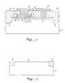
- FIGS. 1 and 18are side sectional views of transistor embodiment in accord with the present invention, with FIG. 1 taken along lines A-A in FIG. 17 and FIG. 18 taken along lines B-B in FIG. 17 .
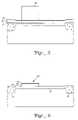
- FIGS. 2-6 , 8 , 9 , 11 - 14 , and 16are side sectional views of the device of FIG. 1 at different stages of construction.
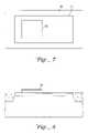
- FIGS. 7 , 10 , 15 , and 17are top plan views of the device of FIG. 1 and FIG. 18 with FIG. 7 corresponding to FIG. 6 , FIG. 10 corresponding to FIG. 9 , FIG. 15 corresponding to FIG. 14 , and FIG. 17 corresponding to FIG. 16 .
- a wafer substrate 11forms a p-type substrate, or a p-well built in an n-type substrate, for the formation of an embodiment of the device of the present invention.
- An equivalent structurewould be an n-type substrate, on an n-well in a p-type substrate, for devices of opposite conductivity type.
- the substrate 11is a lightly doped p-type substrate with an active area for device formation defined by a subsurface boundary demarcated by a shallow trench isolation periphery, particularly trench areas 13 and 15 which extend a short distance below substrate surface 12 .
- a drain region 17is a subsurface electrode that is highly doped n+ region that can be formed either by diffusion or ion implantation, but less deep than trench areas 13 and 15 .
- the drain electrodemost easily extends across the active area, but need not extend the total distance, so long as it extends far enough that it can be reached by a drain contact 43 which is apart from the vertically stacked arrangement of the channel and the source above the drain, described below. While a drain is shown as the subsurface electrode and the source electrode is shown at the top of a vertical electrode stack, the electrodes could be reversed and the source could be the subsurface electrode, with the drain at the top of the stack.
- the drain 17is a composite channel formed by p-type buffer regions 21 and 25 on either side of channel region 23 , which is a p+ region.
- the three composite channel regionsare formed by epitaxially grown undoped or lightly doped silicon, with the p-region 21 being approximately 500-800 angstroms thick, the channel region 23 being approximately 1,000 angstroms thick and the buffer region 25 being approximately 500-800 angstroms thick.
- the height of channel region 23is what defines the channel length between source electrode 27 and a drain electrode 17 .
- the width of the channelis not limited and extends into the paper. A very short channel length, say one nanometer, is theoretically possible without incurring adverse short channel effects due to buffering by channel buffer regions 21 and 25 .
- n+ source region 27is deposited above the composite channel formed by channel region 23 and buffer regions 21 and 25 .
- the doping concentration of the source region 25is similar to the doping concentration of drain 17 and both the source and the drain are of the same conductivity type, while the channel is of an opposite conductivity type so that source and drain p-n junctions exist between the drain and the channel and the channel and the source, typical of FET transistors.
- the vertically stacked sandwich arrangement of drain, channel, and source regionsform a three-dimensional structure extending approximately 3,500 angstroms above the surface of the substrate and extending into the substrate by a few hundred angstroms. Such a three-dimensional transistor structure allows the channel to be scaled by dimensions as small or as large as desired for meeting circuit requirements.
- the channel lengthis defined by the thickness of layers 21 , 23 , and 25 .
- the transistor that is fabricated with the stack sandwich arrangementcan be a standard MOSFET transistor, a nanocrystal memory transistor, or a CMOS transistor.
- a nanocrystal transistoris shown by having a dielectric matrix 29 on lateral sides of the vertically stacked sandwich arrangement in an L-shaped configuration with a portion of the L being upright members abutting the channel, as well as the source, and horizontal portions parallel to the substrate and immediately above the surface 12 .
- the dielectric matrix 29would be ordinary silicon dioxide.
- nanocrystals 31are disposed by any of the usual procedures for dispersing nanocrystals in a dielectric matrix, such as chemical vapor deposition.
- the dielectricforms a charge storage area that would be appropriate for a non-volatile memory transistor.
- the devicecan function in a common MOSFET or a CMOS transistor.
- Controlling the channelare the first and second L-shaped gate members 33 and 35 on either side of the channel and adjacent to the dielectric matrix 29 .
- the first and second L-shaped gate membersare equipotential members, being joined about edges of the stacked arrangement of drain, channel, and source.
- the gatesurrounds the channel on all sides.
- the horizontal portion 28 of the L-shaped gateextends away from the vertical channel structure.
- the gate contactis shaped identically to the drain contact with all three contacts having a vertical component extending generally parallel to the stacked arrangement of the source and channel.
- a source contact 41is a metal member immediately above source 27 .
- Drain contact 43is a metal member which extends through the second gate insulation section 39 and makes contact with drain 17 at surface 12 .
- the upright portion of the gatei.e., the upright portion of first L-shaped gate member 33 and a corresponding portion of the second L-shaped gate member 35 modulate or control current flow between source 27 and drain 17 through channel 25 .
- the upright gate portion 33 and 35can be control gates, controlling charge storage on nanocrystals 31 as charge is pulled from drain 17 onto the nanocrystals by tunneling action, or otherwise, as controlled by voltages on upright portions of the gates 33 and 35 .
- a supplemental thin oxide coatingknown as tunneling oxide may be disposed on the stacked sandwich arrangement of source and channel so that the dielectric matrix 29 supporting nanocrystals 31 could be made very thin. If a memory device is not constructed, the typical thickness for dielectric matrix 29 would be typically 20-50 angstroms.
- Substrate 11is lightly doped silicon, a portion of a standard silicon wafer having shallow trench isolation (STI) regions 13 and 15 which define an active area for construction of a vertical MOS transistor.
- STIshallow trench isolation
- a typical area-wise dimensionis under 90,000 square nanometers if built with 90 nm technology. Such an area is insufficient for building a conventional MOS transistor with channel dimension adequate for avoiding undesired short channel effects.
- a vertical transistor, with a vertical channelwill easily fit in this space, with a channel scaled to be appropriate for the purpose of the transistor and yet have contacts similar in geometry to contacts for a lateral transistor.
- a doped region 17forms a drain spanning the space between isolation regions 13 and 15 below surface 12 .
- Dopingmay be by diffusion or ion implantation.
- the thickness of the doped drain region 17is not critical, and is approximately 400-600 angstroms thick and is a highly doped region, typically an n+ region where substrate 11 is p-type. Of course, polarities could be reversed.
- three epitaxial silicon layersare grown over the subsurface drain region 17 . These layers have a conductivity type opposite that of the drain, p-type in this example.
- the lowermost and uppermost of the three layersare buffer layers for a channel layer which resides between the lowermost and uppermost layers 21 and 25 .
- the lowermost layer 21 and uppermost layer 25 of the three epitaxial layersare each approximately 500-800 angstroms thick and are lightly doped or undoped.
- the height of the channel region 23defines the channel length. This length may be adjusted vertically to be very small or very large and several different devices can be scaled with approximately the same geometry.
- nanocrystal transistorsare described for use as non-volatile memory devices. FET and CMOS transistors could be built using the same geometry, without nanocrystals.
- mask 51defines the cross sectional dimensions of the channel to be formed by the three epitaxial silicon layers 21 , 23 , and 25 . Recall that the length of the channel is defined by the height of layer 23 , but the cross sectional area or widths of the channel is defined by mask 51 .
- isolation perimeter 55surrounds the active area where drain 17 resides over the entirety of the active area.
- the silicon island 53is offset from the center of the active area and will have further layers deposited thereon.
- a thin dielectric layer 61such as a thin high quality gate oxide, approximately 20-50 angstroms thick, is thermally grown over the surface of the layer.
- silicon nanocrystalswill be dispersed on the oxide layer or in a dielectric matrix on the thin oxide layer by the usual techniques, such as chemical vapor deposition. The deposition of nanocrystal layers is extensively described in technical literature.
- a polysilicon layer 63is deposited over the entirety of the substrate covering the silicon island 53 with vertical sidewalls 65 and 67 , as well as horizontal portions 68 and 69 proximate to the subsurface drain 17 .
- a flag-shaped mask 71is placed within the boundary of the polysilicon gate 63 which was shown to be deposited in FIG. 9 .
- the maskdoes not protect quadrant 73 of the die or chip, but protects other quadrants.
- the rectangular border 55represents the isolation parameter of the die or chip, (i.e., active area).
- the polysilicon layer 63is seen to be trimmed by removal of polysilicon over the isolation areas 13 and 15 .
- a nitride layer 71is deposited over the trimmed polysilicon layer 63 in a manner extending over the entire die. This layer is now leveled by chemical-mechanical polishing (CMP), stopping on the polysilicon layer, as shown in FIG. 13 .
- CMPchemical-mechanical polishing
- the upper region of polysilicon, as well as a portion of gate insulator 61will be removed in a rectangular configuration opening a window 89 to the silicon island 53 , as seen in FIGS. 14 and 15 .
- the window 89allows growth of an epitaxial doped silicon layer 81 above the silicon island 53 , seen in FIG. 16 .
- the doping of layer 81is of a second conductivity type, approximately at the same concentration as drain 17 and in the same polarity type for the majority carriers, i.e., n+ type.
- a nitride layer 83is deposited and etched to the shape shown.
- Mask members 82 , 84 , and 86are placed over the nitride layer 81 or oxide (TEOS) layer to define a source contact 83 , as well as a drain contact opening 85 , and a gate contact opening, not seen in FIG. 16 , but seen in the top view of FIG. 17 .
- source contact opening 83extends to the top of the most recently deposited source electrode.
- Opening 85extends to the top of a polysilicon L-shaped gate electrode and contact opening 87 extends to the top of the substrate where contact is made with the drain electrode.
- FIG. 18contact 42 reaches the extension 28 of gate electrode 35 . It can be seen that the three contacts 83 , 85 , and 87 form a planar array for source, gate, and drain electrodes which are arranged in a vertical array.
Landscapes
- Non-Volatile Memory (AREA)
- Insulated Gate Type Field-Effect Transistor (AREA)
- Semiconductor Memories (AREA)
- Metal-Oxide And Bipolar Metal-Oxide Semiconductor Integrated Circuits (AREA)
Abstract
Description
Claims (11)
Priority Applications (7)
| Application Number | Priority Date | Filing Date | Title |
|---|---|---|---|
| US11/123,673US7335943B2 (en) | 2005-05-06 | 2005-05-06 | Ultrascalable vertical MOS transistor with planar contacts |
| CNA2006800155044ACN101171690A (en) | 2005-05-06 | 2006-04-12 | Super-scalable vertical MOS transistors with planar contacts |
| EP06740920AEP1880424A2 (en) | 2005-05-06 | 2006-04-12 | Ultrascalable vertical mos transistor with planar contacts |
| KR1020077028152AKR20080007398A (en) | 2005-05-06 | 2006-04-12 | Ultra Scalable Vertical MOOS Transistor with Flat Contact |
| JP2008510016AJP2008544476A (en) | 2005-05-06 | 2006-04-12 | Ultra-scalable vertical MOS transistor with planar contact |
| PCT/US2006/013799WO2006121566A2 (en) | 2005-05-06 | 2006-04-12 | Ultrascalable vertical mos transistor with planar contacts |
| TW095114847ATW200731550A (en) | 2005-05-06 | 2006-04-26 | Vertical MOS transistor and method of forming the same |
Applications Claiming Priority (1)
| Application Number | Priority Date | Filing Date | Title |
|---|---|---|---|
| US11/123,673US7335943B2 (en) | 2005-05-06 | 2005-05-06 | Ultrascalable vertical MOS transistor with planar contacts |
Publications (2)
| Publication Number | Publication Date |
|---|---|
| US20060249783A1 US20060249783A1 (en) | 2006-11-09 |
| US7335943B2true US7335943B2 (en) | 2008-02-26 |
Family
ID=37393311
Family Applications (1)
| Application Number | Title | Priority Date | Filing Date |
|---|---|---|---|
| US11/123,673Expired - LifetimeUS7335943B2 (en) | 2005-05-06 | 2005-05-06 | Ultrascalable vertical MOS transistor with planar contacts |
Country Status (7)
| Country | Link |
|---|---|
| US (1) | US7335943B2 (en) |
| EP (1) | EP1880424A2 (en) |
| JP (1) | JP2008544476A (en) |
| KR (1) | KR20080007398A (en) |
| CN (1) | CN101171690A (en) |
| TW (1) | TW200731550A (en) |
| WO (1) | WO2006121566A2 (en) |
Families Citing this family (12)
| Publication number | Priority date | Publication date | Assignee | Title |
|---|---|---|---|---|
| US7176084B2 (en)* | 2005-06-09 | 2007-02-13 | Taiwan Semiconductor Manufacturing Co., Ltd. | Self-aligned conductive spacer process for sidewall control gate of high-speed random access memory |
| JP5547429B2 (en)* | 2009-06-19 | 2014-07-16 | ルネサスエレクトロニクス株式会社 | Semiconductor device |
| JP2013026382A (en)* | 2011-07-20 | 2013-02-04 | Elpida Memory Inc | Manufacturing method of semiconductor device |
| US9257347B2 (en)* | 2012-08-30 | 2016-02-09 | Taiwan Semiconductor Manufacturing Company, Ltd. | System and method for a field-effect transistor with a raised drain structure |
| US9461143B2 (en) | 2012-09-19 | 2016-10-04 | Intel Corporation | Gate contact structure over active gate and method to fabricate same |
| US9847233B2 (en)* | 2014-07-29 | 2017-12-19 | Taiwan Semiconductor Manufacturing Company Limited | Semiconductor device and formation thereof |
| WO2018004629A1 (en)* | 2016-06-30 | 2018-01-04 | Intel Corporation | Integrated circuit die having back-end-of-line transistors |
| CN109036487B (en)* | 2018-07-20 | 2021-03-02 | 福州大学 | A kind of multi-level optical memory based on short-channel organic transistor and preparation method thereof |
| US10985272B2 (en)* | 2018-11-05 | 2021-04-20 | Samsung Electronics Co., Ltd. | Integrated circuit devices including vertical field-effect transistors |
| KR102694476B1 (en)* | 2019-08-02 | 2024-08-13 | 양쯔 메모리 테크놀로지스 씨오., 엘티디. | 3D memory devices and their manufacturing methods |
| TWI755734B (en)* | 2020-05-19 | 2022-02-21 | 力晶積成電子製造股份有限公司 | Semiconductor device and method of manufacturing same |
| CN114300542B (en)* | 2021-12-31 | 2022-09-06 | 上海镓芯科技有限公司 | Thin film type vertical structure field effect power transistor |
Citations (10)
| Publication number | Priority date | Publication date | Assignee | Title |
|---|---|---|---|---|
| US4774556A (en) | 1985-07-25 | 1988-09-27 | Nippondenso Co., Ltd. | Non-volatile semiconductor memory device |
| US5395789A (en)* | 1993-08-06 | 1995-03-07 | At&T Corp. | Integrated circuit with self-aligned isolation |
| US5780327A (en)* | 1996-03-05 | 1998-07-14 | International Business Machines Corporation | Vertical double-gate field effect transistor |
| US5821591A (en) | 1996-02-02 | 1998-10-13 | Siemens Aktiengesellschaft | High density read only memory cell configuration and method for its production |
| US5874760A (en)* | 1997-01-22 | 1999-02-23 | International Business Machines Corporation | 4F-square memory cell having vertical floating-gate transistors with self-aligned shallow trench isolation |
| US6313487B1 (en)* | 2000-06-15 | 2001-11-06 | Board Of Regents, The University Of Texas System | Vertical channel floating gate transistor having silicon germanium channel layer |
| US6580124B1 (en) | 2000-08-14 | 2003-06-17 | Matrix Semiconductor Inc. | Multigate semiconductor device with vertical channel current and method of fabrication |
| US6638823B2 (en)* | 2001-03-28 | 2003-10-28 | Electronics And Telecommunications Research Institute | Ultra small size vertical MOSFET device and method for the manufacture thereof |
| US6831310B1 (en) | 2003-11-10 | 2004-12-14 | Freescale Semiconductor, Inc. | Integrated circuit having multiple memory types and method of formation |
| US20050098822A1 (en)* | 2003-11-10 | 2005-05-12 | Leo Mathew | Transistor having three electrically isolated electrodes and method of formation |
Family Cites Families (1)
| Publication number | Priority date | Publication date | Assignee | Title |
|---|---|---|---|---|
| US3874760A (en)* | 1972-04-27 | 1975-04-01 | Bernell J Guthmiller | Sheathed electrical coupling |
- 2005
- 2005-05-06USUS11/123,673patent/US7335943B2/ennot_activeExpired - Lifetime
- 2006
- 2006-04-12JPJP2008510016Apatent/JP2008544476A/ennot_activeWithdrawn
- 2006-04-12KRKR1020077028152Apatent/KR20080007398A/ennot_activeWithdrawn
- 2006-04-12CNCNA2006800155044Apatent/CN101171690A/enactivePending
- 2006-04-12WOPCT/US2006/013799patent/WO2006121566A2/enactiveSearch and Examination
- 2006-04-12EPEP06740920Apatent/EP1880424A2/ennot_activeWithdrawn
- 2006-04-26TWTW095114847Apatent/TW200731550A/enunknown
Patent Citations (10)
| Publication number | Priority date | Publication date | Assignee | Title |
|---|---|---|---|---|
| US4774556A (en) | 1985-07-25 | 1988-09-27 | Nippondenso Co., Ltd. | Non-volatile semiconductor memory device |
| US5395789A (en)* | 1993-08-06 | 1995-03-07 | At&T Corp. | Integrated circuit with self-aligned isolation |
| US5821591A (en) | 1996-02-02 | 1998-10-13 | Siemens Aktiengesellschaft | High density read only memory cell configuration and method for its production |
| US5780327A (en)* | 1996-03-05 | 1998-07-14 | International Business Machines Corporation | Vertical double-gate field effect transistor |
| US5874760A (en)* | 1997-01-22 | 1999-02-23 | International Business Machines Corporation | 4F-square memory cell having vertical floating-gate transistors with self-aligned shallow trench isolation |
| US6313487B1 (en)* | 2000-06-15 | 2001-11-06 | Board Of Regents, The University Of Texas System | Vertical channel floating gate transistor having silicon germanium channel layer |
| US6580124B1 (en) | 2000-08-14 | 2003-06-17 | Matrix Semiconductor Inc. | Multigate semiconductor device with vertical channel current and method of fabrication |
| US6638823B2 (en)* | 2001-03-28 | 2003-10-28 | Electronics And Telecommunications Research Institute | Ultra small size vertical MOSFET device and method for the manufacture thereof |
| US6831310B1 (en) | 2003-11-10 | 2004-12-14 | Freescale Semiconductor, Inc. | Integrated circuit having multiple memory types and method of formation |
| US20050098822A1 (en)* | 2003-11-10 | 2005-05-12 | Leo Mathew | Transistor having three electrically isolated electrodes and method of formation |
Also Published As
| Publication number | Publication date |
|---|---|
| US20060249783A1 (en) | 2006-11-09 |
| JP2008544476A (en) | 2008-12-04 |
| EP1880424A2 (en) | 2008-01-23 |
| TW200731550A (en) | 2007-08-16 |
| KR20080007398A (en) | 2008-01-18 |
| WO2006121566A3 (en) | 2007-02-22 |
| WO2006121566A2 (en) | 2006-11-16 |
| CN101171690A (en) | 2008-04-30 |
Similar Documents
| Publication | Publication Date | Title |
|---|---|---|
| EP1880424A2 (en) | Ultrascalable vertical mos transistor with planar contacts | |
| US8633085B2 (en) | Dual-depth self-aligned isolation structure for a back gate electrode | |
| US9472461B2 (en) | Double gated 4F2 dram CHC cell and methods of fabricating the same | |
| TWI492376B (en) | Fin field effect transistor | |
| US9472613B2 (en) | Conversion of strain-inducing buffer to electrical insulator | |
| US7863136B2 (en) | Method of manufacturing integrated circuits including a FET with a gate spacer and a fin | |
| KR102753006B1 (en) | NOR type memory device and method for manufacturing the same and electronic device including the memory device | |
| US11967626B2 (en) | Field effect transistors with gate fins and method of making the same | |
| US20230337428A1 (en) | Nor-type memory device, method of manufacturing nor-type memory device, and electronic apparatus including memory device | |
| US20070018207A1 (en) | Split gate storage device including a horizontal first gate and a vertical second gate in a trench | |
| US7250340B2 (en) | Method of fabricating programmable structure including discontinuous storage elements and spacer control gates in a trench | |
| US11450768B2 (en) | High voltage field effect transistor with vertical current paths and method of making the same | |
| US12015084B2 (en) | Field effect transistors with gate fins and method of making the same | |
| US20220109070A1 (en) | High voltage field effect transistor with vertical current paths and method of making the same | |
| US20250015188A1 (en) | Triple-gate mos transistor and method for manufacturing such a transistor | |
| US11978774B2 (en) | High voltage field effect transistor with vertical current paths and method of making the same | |
| US7394686B2 (en) | Programmable structure including discontinuous storage elements and spacer control gates in a trench | |
| US20230363153A1 (en) | Nor-type memory device, method of manufacturing nor-type memory device, and electronic apparatus including memory device | |
| US20240040766A1 (en) | Method for fabricating semiconductor structure and semiconductor structure | |
| US20230189520A1 (en) | Split gate non-volatile memory cells, hv and logic devices with finfet structures, and method of making same | |
| US12279445B2 (en) | Field effect transistors with gate fins and method of making the same | |
| US20020168843A1 (en) | Method of forming high density eeprom cell. | |
| WO2022252855A1 (en) | Semiconductor apparatus and manufacturing method therefor, and electronic device having same | |
| US20240250119A1 (en) | High voltage field effect transistors with superjunctions and method of making the same | |
| US20240128330A1 (en) | Integrated circuit devices and methods of manufacturing the same |
Legal Events
| Date | Code | Title | Description |
|---|---|---|---|
| AS | Assignment | Owner name:ATMEL CORPORATION, CALIFORNIA Free format text:ASSIGNMENT OF ASSIGNORS INTEREST;ASSIGNOR:LOJEK, BOHUMIL;REEL/FRAME:016882/0001 Effective date:20050503 | |
| STCF | Information on status: patent grant | Free format text:PATENTED CASE | |
| FPAY | Fee payment | Year of fee payment:4 | |
| AS | Assignment | Owner name:MORGAN STANLEY SENIOR FUNDING, INC. AS ADMINISTRATIVE AGENT, NEW YORK Free format text:PATENT SECURITY AGREEMENT;ASSIGNOR:ATMEL CORPORATION;REEL/FRAME:031912/0173 Effective date:20131206 Owner name:MORGAN STANLEY SENIOR FUNDING, INC. AS ADMINISTRAT Free format text:PATENT SECURITY AGREEMENT;ASSIGNOR:ATMEL CORPORATION;REEL/FRAME:031912/0173 Effective date:20131206 | |
| FPAY | Fee payment | Year of fee payment:8 | |
| AS | Assignment | Owner name:ATMEL CORPORATION, CALIFORNIA Free format text:TERMINATION AND RELEASE OF SECURITY INTEREST IN PATENT COLLATERAL;ASSIGNOR:MORGAN STANLEY SENIOR FUNDING, INC.;REEL/FRAME:038376/0001 Effective date:20160404 | |
| AS | Assignment | Owner name:JPMORGAN CHASE BANK, N.A., AS ADMINISTRATIVE AGENT, ILLINOIS Free format text:SECURITY INTEREST;ASSIGNOR:ATMEL CORPORATION;REEL/FRAME:041715/0747 Effective date:20170208 Owner name:JPMORGAN CHASE BANK, N.A., AS ADMINISTRATIVE AGENT Free format text:SECURITY INTEREST;ASSIGNOR:ATMEL CORPORATION;REEL/FRAME:041715/0747 Effective date:20170208 | |
| AS | Assignment | Owner name:JPMORGAN CHASE BANK, N.A., AS ADMINISTRATIVE AGENT, ILLINOIS Free format text:SECURITY INTEREST;ASSIGNORS:MICROCHIP TECHNOLOGY INCORPORATED;SILICON STORAGE TECHNOLOGY, INC.;ATMEL CORPORATION;AND OTHERS;REEL/FRAME:046426/0001 Effective date:20180529 Owner name:JPMORGAN CHASE BANK, N.A., AS ADMINISTRATIVE AGENT Free format text:SECURITY INTEREST;ASSIGNORS:MICROCHIP TECHNOLOGY INCORPORATED;SILICON STORAGE TECHNOLOGY, INC.;ATMEL CORPORATION;AND OTHERS;REEL/FRAME:046426/0001 Effective date:20180529 | |
| AS | Assignment | Owner name:WELLS FARGO BANK, NATIONAL ASSOCIATION, AS NOTES COLLATERAL AGENT, CALIFORNIA Free format text:SECURITY INTEREST;ASSIGNORS:MICROCHIP TECHNOLOGY INCORPORATED;SILICON STORAGE TECHNOLOGY, INC.;ATMEL CORPORATION;AND OTHERS;REEL/FRAME:047103/0206 Effective date:20180914 Owner name:WELLS FARGO BANK, NATIONAL ASSOCIATION, AS NOTES C Free format text:SECURITY INTEREST;ASSIGNORS:MICROCHIP TECHNOLOGY INCORPORATED;SILICON STORAGE TECHNOLOGY, INC.;ATMEL CORPORATION;AND OTHERS;REEL/FRAME:047103/0206 Effective date:20180914 | |
| MAFP | Maintenance fee payment | Free format text:PAYMENT OF MAINTENANCE FEE, 12TH YEAR, LARGE ENTITY (ORIGINAL EVENT CODE: M1553); ENTITY STATUS OF PATENT OWNER: LARGE ENTITY Year of fee payment:12 | |
| AS | Assignment | Owner name:JPMORGAN CHASE BANK, N.A., AS ADMINISTRATIVE AGENT, DELAWARE Free format text:SECURITY INTEREST;ASSIGNORS:MICROCHIP TECHNOLOGY INC.;SILICON STORAGE TECHNOLOGY, INC.;ATMEL CORPORATION;AND OTHERS;REEL/FRAME:053311/0305 Effective date:20200327 | |
| AS | Assignment | Owner name:MICROSEMI CORPORATION, CALIFORNIA Free format text:RELEASE BY SECURED PARTY;ASSIGNOR:JPMORGAN CHASE BANK, N.A, AS ADMINISTRATIVE AGENT;REEL/FRAME:053466/0011 Effective date:20200529 Owner name:SILICON STORAGE TECHNOLOGY, INC., ARIZONA Free format text:RELEASE BY SECURED PARTY;ASSIGNOR:JPMORGAN CHASE BANK, N.A, AS ADMINISTRATIVE AGENT;REEL/FRAME:053466/0011 Effective date:20200529 Owner name:MICROCHIP TECHNOLOGY INC., ARIZONA Free format text:RELEASE BY SECURED PARTY;ASSIGNOR:JPMORGAN CHASE BANK, N.A, AS ADMINISTRATIVE AGENT;REEL/FRAME:053466/0011 Effective date:20200529 Owner name:MICROSEMI STORAGE SOLUTIONS, INC., ARIZONA Free format text:RELEASE BY SECURED PARTY;ASSIGNOR:JPMORGAN CHASE BANK, N.A, AS ADMINISTRATIVE AGENT;REEL/FRAME:053466/0011 Effective date:20200529 Owner name:ATMEL CORPORATION, ARIZONA Free format text:RELEASE BY SECURED PARTY;ASSIGNOR:JPMORGAN CHASE BANK, N.A, AS ADMINISTRATIVE AGENT;REEL/FRAME:053466/0011 Effective date:20200529 | |
| AS | Assignment | Owner name:WELLS FARGO BANK, NATIONAL ASSOCIATION, MINNESOTA Free format text:SECURITY INTEREST;ASSIGNORS:MICROCHIP TECHNOLOGY INC.;SILICON STORAGE TECHNOLOGY, INC.;ATMEL CORPORATION;AND OTHERS;REEL/FRAME:053468/0705 Effective date:20200529 | |
| AS | Assignment | Owner name:WELLS FARGO BANK, NATIONAL ASSOCIATION, AS COLLATERAL AGENT, MINNESOTA Free format text:SECURITY INTEREST;ASSIGNORS:MICROCHIP TECHNOLOGY INCORPORATED;SILICON STORAGE TECHNOLOGY, INC.;ATMEL CORPORATION;AND OTHERS;REEL/FRAME:055671/0612 Effective date:20201217 | |
| AS | Assignment | Owner name:WELLS FARGO BANK, NATIONAL ASSOCIATION, AS NOTES COLLATERAL AGENT, MINNESOTA Free format text:SECURITY INTEREST;ASSIGNORS:MICROCHIP TECHNOLOGY INCORPORATED;SILICON STORAGE TECHNOLOGY, INC.;ATMEL CORPORATION;AND OTHERS;REEL/FRAME:057935/0474 Effective date:20210528 | |
| AS | Assignment | Owner name:MICROSEMI STORAGE SOLUTIONS, INC., ARIZONA Free format text:RELEASE BY SECURED PARTY;ASSIGNOR:JPMORGAN CHASE BANK, N.A., AS ADMINISTRATIVE AGENT;REEL/FRAME:059333/0222 Effective date:20220218 Owner name:MICROSEMI CORPORATION, ARIZONA Free format text:RELEASE BY SECURED PARTY;ASSIGNOR:JPMORGAN CHASE BANK, N.A., AS ADMINISTRATIVE AGENT;REEL/FRAME:059333/0222 Effective date:20220218 Owner name:ATMEL CORPORATION, ARIZONA Free format text:RELEASE BY SECURED PARTY;ASSIGNOR:JPMORGAN CHASE BANK, N.A., AS ADMINISTRATIVE AGENT;REEL/FRAME:059333/0222 Effective date:20220218 Owner name:SILICON STORAGE TECHNOLOGY, INC., ARIZONA Free format text:RELEASE BY SECURED PARTY;ASSIGNOR:JPMORGAN CHASE BANK, N.A., AS ADMINISTRATIVE AGENT;REEL/FRAME:059333/0222 Effective date:20220218 Owner name:MICROCHIP TECHNOLOGY INCORPORATED, ARIZONA Free format text:RELEASE BY SECURED PARTY;ASSIGNOR:JPMORGAN CHASE BANK, N.A., AS ADMINISTRATIVE AGENT;REEL/FRAME:059333/0222 Effective date:20220218 | |
| AS | Assignment | Owner name:ATMEL CORPORATION, ARIZONA Free format text:RELEASE BY SECURED PARTY;ASSIGNOR:JPMORGAN CHASE BANK, N.A., AS ADMINISTRATIVE AGENT;REEL/FRAME:059262/0105 Effective date:20220218 | |
| AS | Assignment | Owner name:MICROSEMI STORAGE SOLUTIONS, INC., ARIZONA Free format text:RELEASE BY SECURED PARTY;ASSIGNOR:WELLS FARGO BANK, NATIONAL ASSOCIATION, AS NOTES COLLATERAL AGENT;REEL/FRAME:059358/0001 Effective date:20220228 Owner name:MICROSEMI CORPORATION, ARIZONA Free format text:RELEASE BY SECURED PARTY;ASSIGNOR:WELLS FARGO BANK, NATIONAL ASSOCIATION, AS NOTES COLLATERAL AGENT;REEL/FRAME:059358/0001 Effective date:20220228 Owner name:ATMEL CORPORATION, ARIZONA Free format text:RELEASE BY SECURED PARTY;ASSIGNOR:WELLS FARGO BANK, NATIONAL ASSOCIATION, AS NOTES COLLATERAL AGENT;REEL/FRAME:059358/0001 Effective date:20220228 Owner name:SILICON STORAGE TECHNOLOGY, INC., ARIZONA Free format text:RELEASE BY SECURED PARTY;ASSIGNOR:WELLS FARGO BANK, NATIONAL ASSOCIATION, AS NOTES COLLATERAL AGENT;REEL/FRAME:059358/0001 Effective date:20220228 Owner name:MICROCHIP TECHNOLOGY INCORPORATED, ARIZONA Free format text:RELEASE BY SECURED PARTY;ASSIGNOR:WELLS FARGO BANK, NATIONAL ASSOCIATION, AS NOTES COLLATERAL AGENT;REEL/FRAME:059358/0001 Effective date:20220228 | |
| AS | Assignment | Owner name:MICROSEMI STORAGE SOLUTIONS, INC., ARIZONA Free format text:RELEASE BY SECURED PARTY;ASSIGNOR:WELLS FARGO BANK, NATIONAL ASSOCIATION, AS NOTES COLLATERAL AGENT;REEL/FRAME:059863/0400 Effective date:20220228 Owner name:MICROSEMI CORPORATION, ARIZONA Free format text:RELEASE BY SECURED PARTY;ASSIGNOR:WELLS FARGO BANK, NATIONAL ASSOCIATION, AS NOTES COLLATERAL AGENT;REEL/FRAME:059863/0400 Effective date:20220228 Owner name:ATMEL CORPORATION, ARIZONA Free format text:RELEASE BY SECURED PARTY;ASSIGNOR:WELLS FARGO BANK, NATIONAL ASSOCIATION, AS NOTES COLLATERAL AGENT;REEL/FRAME:059863/0400 Effective date:20220228 Owner name:SILICON STORAGE TECHNOLOGY, INC., ARIZONA Free format text:RELEASE BY SECURED PARTY;ASSIGNOR:WELLS FARGO BANK, NATIONAL ASSOCIATION, AS NOTES COLLATERAL AGENT;REEL/FRAME:059863/0400 Effective date:20220228 Owner name:MICROCHIP TECHNOLOGY INCORPORATED, ARIZONA Free format text:RELEASE BY SECURED PARTY;ASSIGNOR:WELLS FARGO BANK, NATIONAL ASSOCIATION, AS NOTES COLLATERAL AGENT;REEL/FRAME:059863/0400 Effective date:20220228 | |
| AS | Assignment | Owner name:MICROSEMI STORAGE SOLUTIONS, INC., ARIZONA Free format text:RELEASE BY SECURED PARTY;ASSIGNOR:WELLS FARGO BANK, NATIONAL ASSOCIATION, AS NOTES COLLATERAL AGENT;REEL/FRAME:059363/0001 Effective date:20220228 Owner name:MICROSEMI CORPORATION, ARIZONA Free format text:RELEASE BY SECURED PARTY;ASSIGNOR:WELLS FARGO BANK, NATIONAL ASSOCIATION, AS NOTES COLLATERAL AGENT;REEL/FRAME:059363/0001 Effective date:20220228 Owner name:ATMEL CORPORATION, ARIZONA Free format text:RELEASE BY SECURED PARTY;ASSIGNOR:WELLS FARGO BANK, NATIONAL ASSOCIATION, AS NOTES COLLATERAL AGENT;REEL/FRAME:059363/0001 Effective date:20220228 Owner name:SILICON STORAGE TECHNOLOGY, INC., ARIZONA Free format text:RELEASE BY SECURED PARTY;ASSIGNOR:WELLS FARGO BANK, NATIONAL ASSOCIATION, AS NOTES COLLATERAL AGENT;REEL/FRAME:059363/0001 Effective date:20220228 Owner name:MICROCHIP TECHNOLOGY INCORPORATED, ARIZONA Free format text:RELEASE BY SECURED PARTY;ASSIGNOR:WELLS FARGO BANK, NATIONAL ASSOCIATION, AS NOTES COLLATERAL AGENT;REEL/FRAME:059363/0001 Effective date:20220228 | |
| AS | Assignment | Owner name:MICROSEMI STORAGE SOLUTIONS, INC., ARIZONA Free format text:RELEASE BY SECURED PARTY;ASSIGNOR:WELLS FARGO BANK, NATIONAL ASSOCIATION, AS NOTES COLLATERAL AGENT;REEL/FRAME:060894/0437 Effective date:20220228 Owner name:MICROSEMI CORPORATION, ARIZONA Free format text:RELEASE BY SECURED PARTY;ASSIGNOR:WELLS FARGO BANK, NATIONAL ASSOCIATION, AS NOTES COLLATERAL AGENT;REEL/FRAME:060894/0437 Effective date:20220228 Owner name:ATMEL CORPORATION, ARIZONA Free format text:RELEASE BY SECURED PARTY;ASSIGNOR:WELLS FARGO BANK, NATIONAL ASSOCIATION, AS NOTES COLLATERAL AGENT;REEL/FRAME:060894/0437 Effective date:20220228 Owner name:SILICON STORAGE TECHNOLOGY, INC., ARIZONA Free format text:RELEASE BY SECURED PARTY;ASSIGNOR:WELLS FARGO BANK, NATIONAL ASSOCIATION, AS NOTES COLLATERAL AGENT;REEL/FRAME:060894/0437 Effective date:20220228 Owner name:MICROCHIP TECHNOLOGY INCORPORATED, ARIZONA Free format text:RELEASE BY SECURED PARTY;ASSIGNOR:WELLS FARGO BANK, NATIONAL ASSOCIATION, AS NOTES COLLATERAL AGENT;REEL/FRAME:060894/0437 Effective date:20220228 |