US7335920B2 - LED with current confinement structure and surface roughening - Google Patents
LED with current confinement structure and surface rougheningDownload PDFInfo
- Publication number
- US7335920B2 US7335920B2US11/042,030US4203005AUS7335920B2US 7335920 B2US7335920 B2US 7335920B2US 4203005 AUS4203005 AUS 4203005AUS 7335920 B2US7335920 B2US 7335920B2
- Authority
- US
- United States
- Prior art keywords
- layer
- led
- type
- confinement structure
- contact
- Prior art date
- Legal status (The legal status is an assumption and is not a legal conclusion. Google has not performed a legal analysis and makes no representation as to the accuracy of the status listed.)
- Expired - Lifetime
Links
Images


Classifications
- H—ELECTRICITY
- H10—SEMICONDUCTOR DEVICES; ELECTRIC SOLID-STATE DEVICES NOT OTHERWISE PROVIDED FOR
- H10H—INORGANIC LIGHT-EMITTING SEMICONDUCTOR DEVICES HAVING POTENTIAL BARRIERS
- H10H20/00—Individual inorganic light-emitting semiconductor devices having potential barriers, e.g. light-emitting diodes [LED]
- H10H20/80—Constructional details
- H10H20/83—Electrodes
- H10H20/832—Electrodes characterised by their material
- H10H20/833—Transparent materials
- H—ELECTRICITY
- H10—SEMICONDUCTOR DEVICES; ELECTRIC SOLID-STATE DEVICES NOT OTHERWISE PROVIDED FOR
- H10H—INORGANIC LIGHT-EMITTING SEMICONDUCTOR DEVICES HAVING POTENTIAL BARRIERS
- H10H20/00—Individual inorganic light-emitting semiconductor devices having potential barriers, e.g. light-emitting diodes [LED]
- H10H20/80—Constructional details
- H10H20/81—Bodies
- H10H20/816—Bodies having carrier transport control structures, e.g. highly-doped semiconductor layers or current-blocking structures
- H10H20/8162—Current-blocking structures
- H—ELECTRICITY
- H10—SEMICONDUCTOR DEVICES; ELECTRIC SOLID-STATE DEVICES NOT OTHERWISE PROVIDED FOR
- H10H—INORGANIC LIGHT-EMITTING SEMICONDUCTOR DEVICES HAVING POTENTIAL BARRIERS
- H10H20/00—Individual inorganic light-emitting semiconductor devices having potential barriers, e.g. light-emitting diodes [LED]
- H10H20/80—Constructional details
- H10H20/81—Bodies
- H10H20/819—Bodies characterised by their shape, e.g. curved or truncated substrates
- H10H20/82—Roughened surfaces, e.g. at the interface between epitaxial layers
- H—ELECTRICITY
- H10—SEMICONDUCTOR DEVICES; ELECTRIC SOLID-STATE DEVICES NOT OTHERWISE PROVIDED FOR
- H10H—INORGANIC LIGHT-EMITTING SEMICONDUCTOR DEVICES HAVING POTENTIAL BARRIERS
- H10H20/00—Individual inorganic light-emitting semiconductor devices having potential barriers, e.g. light-emitting diodes [LED]
- H10H20/80—Constructional details
- H10H20/83—Electrodes
- H10H20/832—Electrodes characterised by their material
- H10H20/835—Reflective materials
Definitions
- This inventionrelates to light emitting diodes (LEDs) and more particularly to new structures for enhancing the extraction of light from LEDs.
- LEDsLight emitting diodes
- LEDsare an important class of solid state devices that convert electric energy to light and generally comprise an active layer of semiconductor material sandwiched between two oppositely doped layers. When a bias is applied across the doped layers, holes and electrons are injected into the active layer where they recombine to generate light. Light is emitted omnidirectionally from the active layer and from all surfaces of the LED.
- the doped and active layersare typically formed on a substrate that can be made of different materials such as silicon (Si), silicon carbide (SiC), and sapphire (Al 2 O 3 ). SiC wafers are often preferred because they have a much closer crystal lattice match to Group-III nitrides, which results in Group III nitride films of higher quality.
- SiCalso has a very high thermal conductivity so that the total output power of Group III nitride devices on SiC is not limited by the thermal resistance of the wafer (as is the case with some devices formed on sapphire or Si). Also, the availability of semi insulating SiC wafers provides the capacity for device isolation and reduced parasitic capacitance that make commercial devices possible. SiC substrates are available from Cree Inc., of Durham, N.C. and methods for producing them are set forth in the scientific literature as well as in U.S. Pat. Nos. Re. 34,861; 4,946,547; and 5,200,022.
- TIRtotal internal reflection
- LEDs with SiC substrateshave relatively low light extraction efficiencies because the high index of refraction of SiC (approximately 2.7) compared to the index of refraction for the surrounding material, such as epoxy (approximately 1.5). This difference results in a small escape cone from which light rays from the active area can transmit from the SiC substrate into the epoxy and ultimately escape from the LED package.
- U.S. Pat. No. 6,410,942assigned to Cree Inc., discloses an LED structure that includes an array of electrically interconnected micro LEDs formed between first and second spreading layers. When a bias is applied across the spreaders, the micro LEDs emit light. Light from each of the micro LEDs reaches a surface after traveling only a short distance, thereby reducing TIR.
- U.S. Pat. No. 6,657,236, also assigned to Cree Inc.discloses structures for enhancing light extraction in LEDs through the use of internal and external optical elements formed in an array.
- the optical elementshave many different shapes, such as hemispheres and pyramids, and may be located on the surface of, or within, various layers of the LED.
- the elementsprovide surfaces from which light refracts or scatters.
- the inventionis directed to LEDs having enhanced light extraction features.
- the LEDincludes a p-type layer of material with an associated p-contact, an n-type layer of material with an associated n-contact and an active region between the p-type layer and the n-type layer.
- the LEDfurther includes a confinement structure that is formed within at least one of the p-type layer of material and the n-type layer of material.
- the confinement structuresubstantially prevents the emission of light from the area of the active region that is coincident with the area of the confinement structure.
- the LEDalso includes a roughened surface that is associated with one of the p-type and n-type layers of material.
- the LEDin another aspect of the invention, includes a first layer of material with an associated first contact and first surface through which light is emitted, a second layer of material with an associated second contact and an active region between the first layer and the second layer.
- the LEDfurther includes a confinement structure that is integral with one of the first layer and the second layer.
- the confinement structureis generally axially aligned with the first contact and substantially prevents the emission of light in the area of the active region that is coincident with the area of the confinement structure.
- the LEDincludes a first layer of material with an associated first contact and first surface through which light is emitted, a second layer of material, an active region between the first layer and the second layer, and a conducting substrate adjacent the second layer of material that has an associated substrate contact.
- the LEDfurther includes at least one confinement structure that is within one of the first layer, the second layer and the substrate.
- the confinement structureis generally axially aligned with the first contact and directs current flowing toward the active region away from the area of the active region that is coincident with the area of the confinement structure.
- the LEDincludes a first layer of material with an associated first contact and first surface through which light is emitted, a second layer of material with an associated second contact and an active region between the first layer and the second layer.
- the LEDfurther includes a confinement structure that is associated with the second contact. The confinement structure directs current flowing toward the active region away from the area of the active region that is coincident with the area of the confinement structure.
- FIG. 1is a cross section of one general embodiment of an LED including an active region between two layers of conducting material and a current confinement structure that may be located in either layer of the conducting material;
- FIG. 2is a cross section of another general embodiment of an LED including an active region between two layers of conducting material, a substrate, a roughened top surface and a current confinement structure that may be located in either layer of the conducting material or a substrate;
- FIG. 3is a cross section of a configuration of the LED of FIG. 1 , including a current confinement structure in a bottom layer of n-type material;
- FIG. 4is a cross section of a configuration of the LED of FIG. 2 , including a current confinement structure in a top layer of p-type material and a layer of transparent conducting material having a roughened top surface;
- FIG. 5is a cross section of a configuration of the LED of FIG. 1 , including a current confinement structure in a bottom layer of p-type material and a layer of n-type material having a roughened top surface;
- FIG. 6is a cross section of a configuration of the LED of FIG. 1 , including a current confinement structure in a top layer of n-type material and a layer of n-type material having a roughened top surface;
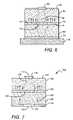
- FIG. 7is a cross section of another general embodiment of an LED including an active region between two layers of conducting material, a top side contact, a bottom side contact and a current confinement structure located in the layer of the bottom side contact.
- the present inventionprovides improved light extraction for light emitting diodes (LEDs) through a confinement structure that is formed within at least one of the p-type layer of material and the n-type layer of material of a base LED structure.
- the confinement structureis generally aligned with the contact on the top and primary emission surface of the LED and substantially prevents the emission of light from the area of the active region that is coincident with the area of the confinement structure and the top-surface contact.
- the current confinement structureis formed within the base LED structure using ion implantation.
- the current confinement structuremay also be formed in the LED base structure using selective oxidation.
- the current confinement structuremay also be formed as part of the LED structure using epitaxial regrowth.
- the LEDmay further include a roughed surface around the absorbing contact.
- the roughened surfacemay be included in all or a portion of the surface area of a layer of the base LED structure or in all or a portion of the surface area of an additional layer of material applied to the base LED structure.
- a layer of transparent materialmay be added to the p-type layer and roughen that layer.
- a layer of transparent materialmay also be added to the n-type layer of an n-side up LED structure.
- the combination of a roughened surface and current confinement structure that directs current toward the roughened surface and away from the absorbing contactprovides further enhanced light extraction.
- the roughened surfaceimproves light extraction by providing a varying surface that allows light that would otherwise be trapped in the LED by total internal reflection to escape and contribute to light emission.
- an LED 10including a first layer of material 12 having a first surface 14 through which light is emitted, a second layer of material 16 , and a layer of active material 18 sandwiched between the first layer and the second layer.
- the first layer 12 , second layer 16 and active layer 18form a base LED structure that is positioned on a support structure 36 .
- the base LED structuremay be fabricated from different semiconductor material systems such as the Group III nitride based material systems.
- Group III nitridesrefer to those semiconductor compounds formed between nitrogen and the elements in the Group III of the periodic table, usually aluminum (Al), gallium (Ga), and indium (In).
- Alaluminum
- Gagallium
- Inindium
- the termalso refers to ternary and tertiary compounds such as AlGaN and AlInGaN.
- the layer of active material 18is in adjacent contact with the first layer 12 and the second layer 16 , and the material forming the first and second layers is GaN, with either of the first or second layers being p-type material and the other layer being n-type material.
- the material forming the active layeris InGaN.
- the first and second layer materialmay be AlGaN, AlGaAs or AlGaInP.
- the support structure 36which may be a substrate or a submount.
- the support structure 36would be a substrate, with a suitable substrate being a 4H polytype of silicon carbide, although other silicon carbide polytypes can also be used including 3C, 6H and 15R polytypes.
- Silicon carbidehas a much closer crystal lattice match to Group III nitrides than sapphire and results in Group III nitride films of higher quality. Silicon carbide also has a very high thermal conductivity so that the total output power of Group III nitride devices on silicon carbide is not limited by the thermal dissipation of the substrate (as may be the case with some devices formed on sapphire).
- SiC substratesare available from Cree, Inc., of Durham, N.C. and methods for producing them are set forth in the scientific literature as well as in a U.S. Pat. Nos. Re. 34,861; 4,946,547; and 5,200,022.
- the support structure 36would be a submount.
- a first contact 22is associated with the first layer 12 and a second contact 24 is associated with the second layer 16 .
- the association of the contacts 22 , 24 with their respective layers 12 , 16may be direct or indirect.
- a direct associationwherein the first contact is in direct contact with the first layer 12 and the second contact 24 is in direct contact with the second layer 16 , is shown in FIG. 1 .
- this associationmay be present when the substrate 36 is formed of a non-conducting material.
- Indirect associationsare shown in FIG. 2 and may be present, with respect to the first contact 22 , if the LED includes a layer of transparent conducting material 25 , and for the second contact 24 , if the support structure 36 is a substrate formed of a conducting material.
- the second contactmay be formed of a reflective material, such as silver (Ag), aluminum (Al) or rhodium (Rh).
- a current confinement structure 20is integral with and can be formed in different location within the LED, such as within at least one of the first layer 12 , the second layer 16 or the substrate 36 (as shown in FIG. 2 ). In some embodiments, more than one current confinement structure may be used and in one embodiment the current confinement structure 20 may be formed in both the first layer 12 and the second layer 16 with a portion of the active material 18 between the confinement structures 20 . In some embodiments, the confinement structure 20 may be a region of the layer of material whose crystal structure or molecular properties have been altered through processes known in the art, such as ion implantation or oxidation.
- the confinement structure 20may be a current blocking layer formed from a material that is oppositely doped relative to the material of the first or second layers 12 , 16 .
- This current blocking layer of materialmay be incorporated into one or more of the first and second layers through the known process of epitaxial regrowth.
- the current confinement structure 20is positioned relative to the first contact 22 such that the center 26 or axis of the first contact is generally aligned with the center or axis 28 of the confinement structure.
- the cross-sectional area size of the confinement structure 20essentially mirrors that of the first contact 22 .
- the thickness of the current confinement structure 20may range anywhere from between 0.1% to 80% of the total thickness of the layer. For example, in an n-type layer of material 1 micron thick, the current confinement structure 20 may be between 0.001 and 0.8 microns thick.
- the current confinement structure 20directs current 30 that is flowing toward the active region 18 away from the portion 32 of the active region that is substantially coincident with and aligned with the first contact 22 . This redirection of current substantially prevents the recombination of current charges, i.e., “holes” and “electrons,” in the portion 32 of the active region aligned with the first contact 22 , thus essentially rendering the region inactive.
- Light 34is emitted from the active material 18 and propagates through the LED structure. Although, light emits from the active material 18 in all directions, for ease of illustration, light in the figures is shown only in the upward direction toward the top or primary emission surface of the LED.
- the top surfaceis the surface 14 of the top layer of material 12 .
- the top surfaceis a layer of roughened material 25 .
- one embodiment of the general LED of FIG. 1is shown comprising a p-side up LED that includes a first layer 40 of p-type material and a second layer 42 of n-type material.
- the materialis GaN.
- the current confinement structure 44is incorporated into the n-type material layer 42 .
- the structure 44is formed by introducing impurities into the n-type material. The introduction of impurities may be done by ion implantation. For example, for an n-type GaN material, either Al or Ga ions may be implanted.
- the current moving through the p-type material 40also moves away from the current confinement structure 44 and into the areas of the active region where the current from the n-type material has entered.
- This movement of the p-type material currentis a result of a combination of both the presence of the current confinement structure 44 in the n-type material and the attraction of the p-type current “holes” to the n-type current “electrons” present in the active portion 52 of the active region 50 .
- the current confinement structure 44may be positioned at any one of several locations along the depth of the n-type layer 42 . This may be done by interrupting the growth process of the n-type layer 42 , implanting the impurities into the incomplete n-type layer and then resuming the growth process to complete the rest of the n-type layer.
- the growth processmay be any one of various known processes including metal oxide chemical vapor deposition (MOCVD), hybrid vapor phase epitaxy (HVPE) or molecular beam epitaxy (MBE).
- An exemplary confinement structure formation processincludes implanting the n-layer with 180 keV aluminum ions in doses of 10 13 , 10 14 and 10 15 cm ⁇ 2 .
- the current confinement structure 44is located close to active region 50 to effectively prevent n-type current from moving completely around the current confinement structure and back toward the inactive region 54 , and to increase the affect of the structure on the current in the p-type layer on the opposite side of the active region 50 .
- FIG. 4another embodiment of the general LED 10 of FIG. 2 according to the present invention is shown comprising a p-side up LED that is essentially the same as that described with reference to FIG. 3 , except the current confinement structure 44 is located in the p-type layer 40 . Also, the substrate 58 is conducting thus allowing for an indirect association between the n-contact 48 and the n-type layer 42 . A layer of transparent conducting material 56 is included on the p-type layer 40 with a portion of the conducting material layer sandwiched between the p-contact 46 and the p-type layer. This layer of material may be formed from ZnO, In 2 O 3 and indium tin oxide (ITO).
- ITOindium tin oxide
- At least part of the conducting material layer 56 not covered by the p-contact 46is roughened, with all of the top surface of the conducting material layer as shown in FIG. 4 being roughened.
- the combination of the layer of transparent conducting material 56 and localized light generation away from the absorbing contact 46 , provided by the current confinement structure 44increases the light extraction efficiency of the LED.
- FIG. 5another embodiment of the general LED 10 of FIG. 1 is shown, comprising an n-side up, flip-chip LED that includes a first layer 60 of n-type material and a second layer 62 of p-type material.
- the substrate which is typically adjacent to the first n-type layer 60is removed to reveal the top primary emitting surface of the LED.
- the LED materialis GaN.
- the current confinement structure 64is incorporated into the p-type material layer 62 prior to flipping layers 60 , 62 , 64 and p-contact substructure onto a submount 78 .
- the confinement structure 64is formed by introducing impurities into the p-type material by ion implantation during growth. For example, for a p-type GaN material, either Al or Ga ions may be implanted.
- the top surface 66 of the n-type layeris roughened to form a roughened light extraction surface.
- the roughened surfacemay be provided by etching, using any one of several methods known in the art, such as photoelectrochemical (PEC) etching. In this configuration, the roughened surface is added directly to the n-type layer instead of through a separately added layer of transparent conducting material, as is typically required for p-side up LEDs, due to the relative thinness of the p-layer.
- PECphotoelectrochemical
- the current confinement structure 64may be positioned at various locations along the depth of the p-type layer 62 by interrupting the growth process of the p-type layer, implanting the impurities into the incomplete p-type layer and then resuming the growth process to complete the layer.
- the current confinement structure 64is located close to active region 72 to effectively prevent p-type current from moving completely around the current confinement structure and back toward the inactive region 76 , and to increase the affect of the structure on the current in the n-type layer on the opposite side of the active region 72 .
- the general LED of FIG. 1is an n-side up LED that is essentially the same as that described with reference to FIG. 5 , except the current confinement structure 64 is located in the n-type layer 60 .
- an LED 100including a first layer of material 102 having a first surface 104 through which most of the light is emitted, a second layer of material 106 and a layer of active material 108 sandwiched between the first layer and the second layer.
- the layer of active material 108is in adjacent contact with the first layer 102 and the second layer 106 , and the material forming the first and second layers is GaN and the material forming the active layer is InGaN.
- the first and second layer materialmay be AlGaN, AlGaAs or AlGaInP.
- a first contact 110is associated with the first layer 102 and a second contact 112 is associated with the second layer 106 .
- a current confinement structure 114is included in the layer of the second contact 112 and is positioned relative to the first contact 110 such that the center 116 or axis of the first contact is generally aligned with the center or axis 118 of the confinement structure.
- the layer of the second contact 112 and the confinement structure 114is formed by depositing a layer of contact material, etching away a portion of the layer of contact material and replacing it with the material of the confinement structure.
- the confinement structure 114is formed of an insulating, non-conducting material, such as SiO 2 , AlN and SiN, and has a cross-sectional area size essentially the same as that of the first contact 110 .
- the current confinement structure 114directs current 120 that is flowing toward the active region 108 away from the portion 122 of the active region that is substantially coincident with and aligned with the first contact 110 . This redirection of current substantially prevents the recombination of current charges, i.e., “holes” and “electrons,” in the portion 122 of the active region aligned with the first contact 110 , thus essentially rendering the region inactive.
- the general LED of FIG. 7may be formed such that the first layer 102 is either one of an n-type layer or a p-type layer and the second layer 106 is a type of layer opposite that of the first layer.
- the LED 100may also include a surface roughening, either in the form of a roughened top surface of the first layer 102 or an additional layer of transparent conducting material having a roughened top surface.
- FIGS. 1-7may be incorporated into other LED configurations.
- the LEDs of FIGS. 1-7have contacts in a vertical arrangement, i.e., on opposite sides of the LED
- the inventionmay be applied to LEDs having laterally arranged contacts, i.e., on the same side of the LED, such as resonant cavity LEDs.
Landscapes
- Led Devices (AREA)
Abstract
Description
Claims (26)
Priority Applications (14)
| Application Number | Priority Date | Filing Date | Title |
|---|---|---|---|
| US11/042,030US7335920B2 (en) | 2005-01-24 | 2005-01-24 | LED with current confinement structure and surface roughening |
| AT05806491TATE524838T1 (en) | 2005-01-24 | 2005-09-15 | LED WITH CURRENT LIMITING STRUCTURE AND SURFACE ROUGHENING |
| TW094131846ATWI372471B (en) | 2005-01-24 | 2005-09-15 | Led with current confinement structure and surface roughening |
| JP2007552114AJP2008529271A (en) | 2005-01-24 | 2005-09-15 | LED with current confinement structure and rough surface treatment |
| CNA2005800470913ACN101107720A (en) | 2005-01-24 | 2005-09-15 | Light-emitting diodes using current confinement structures and surface roughening |
| EP10181491.1AEP2267803B1 (en) | 2005-01-24 | 2005-09-15 | LED with current confinement structure and surface roughening |
| PCT/US2005/036552WO2006080958A1 (en) | 2005-01-24 | 2005-09-15 | Led with curent confinement structure and surface roughening |
| EP05806491AEP1849193B1 (en) | 2005-01-24 | 2005-09-15 | LED with current confinement structure and surface roughening |
| US11/983,515US8410490B2 (en) | 2005-01-24 | 2007-11-09 | LED with current confinement structure and surface roughening |
| US12/079,486US8410499B2 (en) | 2005-01-24 | 2008-03-25 | LED with a current confinement structure aligned with a contact |
| US12/581,759US8541788B2 (en) | 2005-01-24 | 2009-10-19 | LED with current confinement structure and surface roughening |
| JP2011117143AJP5887068B2 (en) | 2005-01-24 | 2011-05-25 | LED with current confinement structure and rough surface treatment |
| JP2011117144AJP5887069B2 (en) | 2005-01-24 | 2011-05-25 | LED with current confinement structure and rough surface treatment |
| US13/974,505US8772792B2 (en) | 2005-01-24 | 2013-08-23 | LED with surface roughening |
Applications Claiming Priority (1)
| Application Number | Priority Date | Filing Date | Title |
|---|---|---|---|
| US11/042,030US7335920B2 (en) | 2005-01-24 | 2005-01-24 | LED with current confinement structure and surface roughening |
Related Child Applications (1)
| Application Number | Title | Priority Date | Filing Date |
|---|---|---|---|
| US11/983,515DivisionUS8410490B2 (en) | 2005-01-24 | 2007-11-09 | LED with current confinement structure and surface roughening |
Publications (2)
| Publication Number | Publication Date |
|---|---|
| US20060163586A1 US20060163586A1 (en) | 2006-07-27 |
| US7335920B2true US7335920B2 (en) | 2008-02-26 |
Family
ID=36228795
Family Applications (5)
| Application Number | Title | Priority Date | Filing Date |
|---|---|---|---|
| US11/042,030Expired - LifetimeUS7335920B2 (en) | 2005-01-24 | 2005-01-24 | LED with current confinement structure and surface roughening |
| US11/983,515Expired - LifetimeUS8410490B2 (en) | 2005-01-24 | 2007-11-09 | LED with current confinement structure and surface roughening |
| US12/079,486Expired - LifetimeUS8410499B2 (en) | 2005-01-24 | 2008-03-25 | LED with a current confinement structure aligned with a contact |
| US12/581,759Expired - LifetimeUS8541788B2 (en) | 2005-01-24 | 2009-10-19 | LED with current confinement structure and surface roughening |
| US13/974,505Expired - LifetimeUS8772792B2 (en) | 2005-01-24 | 2013-08-23 | LED with surface roughening |
Family Applications After (4)
| Application Number | Title | Priority Date | Filing Date |
|---|---|---|---|
| US11/983,515Expired - LifetimeUS8410490B2 (en) | 2005-01-24 | 2007-11-09 | LED with current confinement structure and surface roughening |
| US12/079,486Expired - LifetimeUS8410499B2 (en) | 2005-01-24 | 2008-03-25 | LED with a current confinement structure aligned with a contact |
| US12/581,759Expired - LifetimeUS8541788B2 (en) | 2005-01-24 | 2009-10-19 | LED with current confinement structure and surface roughening |
| US13/974,505Expired - LifetimeUS8772792B2 (en) | 2005-01-24 | 2013-08-23 | LED with surface roughening |
Country Status (7)
| Country | Link |
|---|---|
| US (5) | US7335920B2 (en) |
| EP (2) | EP2267803B1 (en) |
| JP (3) | JP2008529271A (en) |
| CN (1) | CN101107720A (en) |
| AT (1) | ATE524838T1 (en) |
| TW (1) | TWI372471B (en) |
| WO (1) | WO2006080958A1 (en) |
Cited By (95)
| Publication number | Priority date | Publication date | Assignee | Title |
|---|---|---|---|---|
| US20070152230A1 (en)* | 2006-01-05 | 2007-07-05 | Duong Dung T | Separate optical device for directing light from an LED |
| US20080008964A1 (en)* | 2006-07-05 | 2008-01-10 | Chia-Hua Chan | Light emitting diode and method of fabricating a nano/micro structure |
| US20080081531A1 (en)* | 2006-10-02 | 2008-04-03 | Duong Dung T | LED system and method |
| US20080173887A1 (en)* | 2005-03-28 | 2008-07-24 | Stanley Electric Co., Ltd. | Self-luminous device |
| US20090267083A1 (en)* | 2008-04-28 | 2009-10-29 | Jie Cui | Trenched substrate for crystal growth and wafer bonding |
| US20090275266A1 (en)* | 2006-10-02 | 2009-11-05 | Illumitex, Inc. | Optical device polishing |
| US20090289263A1 (en)* | 2008-02-08 | 2009-11-26 | Illumitex, Inc. | System and Method for Emitter Layer Shaping |
| US20100148193A1 (en)* | 2008-12-11 | 2010-06-17 | Illumitex, Inc. | Systems and methods for packaging light-emitting diode devices |
| US20100207160A1 (en)* | 2009-02-16 | 2010-08-19 | Hyung Jo Park | Semiconductor light emitting device |
| US20100252840A1 (en)* | 2009-04-06 | 2010-10-07 | Cree, Inc. | High voltage low current surface emitting led |
| US20100314649A1 (en)* | 2009-06-10 | 2010-12-16 | Bridgelux, Inc. | Thin-film led with p and n contacts electricall isolated from the substrate |
| US20110044022A1 (en)* | 2009-08-20 | 2011-02-24 | Illumitex, Inc. | System and method for a phosphor coated lens |
| US20110050681A1 (en)* | 2009-08-27 | 2011-03-03 | Novatek Microelectronics Corp. | Low voltage differential signal output stage |
| US20110084294A1 (en)* | 2007-11-14 | 2011-04-14 | Cree, Inc. | High voltage wire bond free leds |
| US20110121357A1 (en)* | 2009-11-25 | 2011-05-26 | Steven Lester | LED with Improved Injection Efficiency |
| US20110198664A1 (en)* | 2010-02-12 | 2011-08-18 | Dae Sung Kang | Light emitting device and light emitting device package including the same |
| WO2011115529A1 (en) | 2010-03-15 | 2011-09-22 | Yuri Georgievich Shreter | Light-emitting device with heterophase boundaries |
| US8096671B1 (en) | 2009-04-06 | 2012-01-17 | Nmera, Llc | Light emitting diode illumination system |
| US8154039B2 (en) | 2004-09-22 | 2012-04-10 | Cree, Inc. | High efficiency group III nitride LED with lenticular surface |
| US20120138991A1 (en)* | 2005-06-21 | 2012-06-07 | Epistar Corporation | High-efficiency light-emitting device and manufacturing method thereof |
| WO2012115541A2 (en) | 2011-02-24 | 2012-08-30 | Yury Georgievich Shreter | Light-emitting semiconductor device |
| US8395165B2 (en) | 2011-07-08 | 2013-03-12 | Bridelux, Inc. | Laterally contacted blue LED with superlattice current spreading layer |
| US8455882B2 (en) | 2010-10-15 | 2013-06-04 | Cree, Inc. | High efficiency LEDs |
| US8552465B2 (en) | 2011-11-09 | 2013-10-08 | Toshiba Techno Center Inc. | Method for reducing stress in epitaxial growth |
| US8558247B2 (en) | 2011-09-06 | 2013-10-15 | Toshiba Techno Center Inc. | GaN LEDs with improved area and method for making the same |
| US8581267B2 (en) | 2011-11-09 | 2013-11-12 | Toshiba Techno Center Inc. | Series connected segmented LED |
| US8585253B2 (en) | 2009-08-20 | 2013-11-19 | Illumitex, Inc. | System and method for color mixing lens array |
| US8597962B2 (en) | 2010-03-31 | 2013-12-03 | Varian Semiconductor Equipment Associates, Inc. | Vertical structure LED current spreading by implanted regions |
| US8624482B2 (en) | 2011-09-01 | 2014-01-07 | Toshiba Techno Center Inc. | Distributed bragg reflector for reflecting light of multiple wavelengths from an LED |
| US8664679B2 (en) | 2011-09-29 | 2014-03-04 | Toshiba Techno Center Inc. | Light emitting devices having light coupling layers with recessed electrodes |
| US8669585B1 (en) | 2011-09-03 | 2014-03-11 | Toshiba Techno Center Inc. | LED that has bounding silicon-doped regions on either side of a strain release layer |
| US8674389B2 (en) | 2010-02-08 | 2014-03-18 | Lg Innotek Co., Ltd. | Light emitting device and light emitting device package having the same |
| US8686430B2 (en) | 2011-09-07 | 2014-04-01 | Toshiba Techno Center Inc. | Buffer layer for GaN-on-Si LED |
| US8698163B2 (en) | 2011-09-29 | 2014-04-15 | Toshiba Techno Center Inc. | P-type doping layers for use with light emitting devices |
| US8704240B2 (en)* | 2004-06-30 | 2014-04-22 | Cree, Inc. | Light emitting devices having current reducing structures |
| US8772792B2 (en) | 2005-01-24 | 2014-07-08 | Cree, Inc. | LED with surface roughening |
| US8814376B2 (en) | 2012-09-26 | 2014-08-26 | Apogee Translite, Inc. | Lighting devices |
| US8853668B2 (en) | 2011-09-29 | 2014-10-07 | Kabushiki Kaisha Toshiba | Light emitting regions for use with light emitting devices |
| US8865565B2 (en) | 2011-08-02 | 2014-10-21 | Kabushiki Kaisha Toshiba | LED having a low defect N-type layer that has grown on a silicon substrate |
| US8916906B2 (en) | 2011-07-29 | 2014-12-23 | Kabushiki Kaisha Toshiba | Boron-containing buffer layer for growing gallium nitride on silicon |
| US8981403B2 (en) | 2011-09-06 | 2015-03-17 | Sensor Electronic Technology, Inc. | Patterned substrate design for layer growth |
| US9012921B2 (en) | 2011-09-29 | 2015-04-21 | Kabushiki Kaisha Toshiba | Light emitting devices having light coupling layers |
| US9012939B2 (en) | 2011-08-02 | 2015-04-21 | Kabushiki Kaisha Toshiba | N-type gallium-nitride layer having multiple conductive intervening layers |
| US9048378B2 (en) | 2011-06-15 | 2015-06-02 | Sensor Electronic Technology, Inc. | Device with inverted large scale light extraction structures |
| US9070833B2 (en) | 2011-08-04 | 2015-06-30 | Kabushiki Kaisha Toshiba | Distributed current blocking structures for light emitting diodes |
| US9093293B2 (en) | 2009-04-06 | 2015-07-28 | Cree, Inc. | High voltage low current surface emitting light emitting diode |
| US9130068B2 (en) | 2011-09-29 | 2015-09-08 | Manutius Ip, Inc. | Light emitting devices having dislocation density maintaining buffer layers |
| US9142741B2 (en) | 2011-06-15 | 2015-09-22 | Sensor Electronic Technology, Inc. | Emitting device with improved extraction |
| US9142743B2 (en) | 2011-08-02 | 2015-09-22 | Kabushiki Kaisha Toshiba | High temperature gold-free wafer bonding for light emitting diodes |
| US9159869B2 (en) | 2011-08-03 | 2015-10-13 | Kabushiki Kaisha Toshiba | LED on silicon substrate using zinc-sulfide as buffer layer |
| US9178114B2 (en) | 2011-09-29 | 2015-11-03 | Manutius Ip, Inc. | P-type doping layers for use with light emitting devices |
| US9324560B2 (en) | 2011-09-06 | 2016-04-26 | Sensor Electronic Technology, Inc. | Patterned substrate design for layer growth |
| US9337387B2 (en) | 2011-06-15 | 2016-05-10 | Sensor Electronic Technology, Inc. | Emitting device with improved extraction |
| US9343641B2 (en) | 2011-08-02 | 2016-05-17 | Manutius Ip, Inc. | Non-reactive barrier metal for eutectic bonding process |
| US9437783B2 (en) | 2012-05-08 | 2016-09-06 | Cree, Inc. | Light emitting diode (LED) contact structures and process for fabricating the same |
| US9543490B2 (en) | 2010-09-24 | 2017-01-10 | Seoul Semiconductor Co., Ltd. | Wafer-level light emitting diode package and method of fabricating the same |
| US9617656B2 (en) | 2011-07-25 | 2017-04-11 | Toshiba Corporation | Nucleation of aluminum nitride on a silicon substrate using an ammonia preflow |
| US9741899B2 (en) | 2011-06-15 | 2017-08-22 | Sensor Electronic Technology, Inc. | Device with inverted large scale light extraction structures |
| US10032956B2 (en) | 2011-09-06 | 2018-07-24 | Sensor Electronic Technology, Inc. | Patterned substrate design for layer growth |
| US10121937B2 (en) | 2012-06-01 | 2018-11-06 | Lumileds Llc | Light extraction using feature size and shape control in LED surface roughening |
| USD847415S1 (en) | 2014-02-18 | 2019-04-30 | DMF, Inc. | Unified casting light module |
| USD847414S1 (en) | 2015-05-29 | 2019-04-30 | DMF, Inc. | Lighting module |
| USD848375S1 (en) | 2015-10-05 | 2019-05-14 | DMF, Inc. | Electrical junction box |
| US10319881B2 (en) | 2011-06-15 | 2019-06-11 | Sensor Electronic Technology, Inc. | Device including transparent layer with profiled surface for improved extraction |
| US10408395B2 (en) | 2013-07-05 | 2019-09-10 | DMF, Inc. | Recessed lighting systems |
| US10461221B2 (en) | 2016-01-18 | 2019-10-29 | Sensor Electronic Technology, Inc. | Semiconductor device with improved light propagation |
| USD864877S1 (en) | 2019-01-29 | 2019-10-29 | DMF, Inc. | Plastic deep electrical junction box with a lighting module mounting yoke |
| US10488000B2 (en) | 2017-06-22 | 2019-11-26 | DMF, Inc. | Thin profile surface mount lighting apparatus |
| US10522714B2 (en) | 2011-06-15 | 2019-12-31 | Sensor Electronic Technology, Inc. | Device with inverted large scale light extraction structures |
| US10551044B2 (en) | 2015-11-16 | 2020-02-04 | DMF, Inc. | Recessed lighting assembly |
| US10563850B2 (en) | 2015-04-22 | 2020-02-18 | DMF, Inc. | Outer casing for a recessed lighting fixture |
| US10580929B2 (en) | 2016-03-30 | 2020-03-03 | Seoul Viosys Co., Ltd. | UV light emitting diode package and light emitting diode module having the same |
| US10663153B2 (en) | 2017-12-27 | 2020-05-26 | DMF, Inc. | Methods and apparatus for adjusting a luminaire |
| US10753558B2 (en) | 2013-07-05 | 2020-08-25 | DMF, Inc. | Lighting apparatus and methods |
| US10763405B2 (en)* | 2014-05-21 | 2020-09-01 | Nichia Corporation | Light emitting device and method of manufacturing the same |
| USD901398S1 (en) | 2019-01-29 | 2020-11-10 | DMF, Inc. | Plastic deep electrical junction box |
| USD902871S1 (en) | 2018-06-12 | 2020-11-24 | DMF, Inc. | Plastic deep electrical junction box |
| USD905327S1 (en) | 2018-05-17 | 2020-12-15 | DMF, Inc. | Light fixture |
| US10975570B2 (en) | 2017-11-28 | 2021-04-13 | DMF, Inc. | Adjustable hanger bar assembly |
| US11060705B1 (en) | 2013-07-05 | 2021-07-13 | DMF, Inc. | Compact lighting apparatus with AC to DC converter and integrated electrical connector |
| US11067231B2 (en) | 2017-08-28 | 2021-07-20 | DMF, Inc. | Alternate junction box and arrangement for lighting apparatus |
| US11231154B2 (en) | 2018-10-02 | 2022-01-25 | Ver Lighting Llc | Bar hanger assembly with mating telescoping bars |
| US11255497B2 (en) | 2013-07-05 | 2022-02-22 | DMF, Inc. | Adjustable electrical apparatus with hangar bars for installation in a building |
| USD945054S1 (en) | 2017-06-22 | 2022-03-01 | DMF, Inc. | Light fixture |
| US11274821B2 (en) | 2019-09-12 | 2022-03-15 | DMF, Inc. | Lighting module with keyed heat sink coupled to thermally conductive trim |
| US11306903B2 (en) | 2020-07-17 | 2022-04-19 | DMF, Inc. | Polymer housing for a lighting system and methods for using same |
| US11391442B2 (en) | 2018-06-11 | 2022-07-19 | DMF, Inc. | Polymer housing for a recessed lighting system and methods for using same |
| US11435064B1 (en) | 2013-07-05 | 2022-09-06 | DMF, Inc. | Integrated lighting module |
| USD966877S1 (en) | 2019-03-14 | 2022-10-18 | Ver Lighting Llc | Hanger bar for a hanger bar assembly |
| USD970081S1 (en) | 2018-05-24 | 2022-11-15 | DMF, Inc. | Light fixture |
| US11585517B2 (en) | 2020-07-23 | 2023-02-21 | DMF, Inc. | Lighting module having field-replaceable optics, improved cooling, and tool-less mounting features |
| USD990030S1 (en) | 2020-07-17 | 2023-06-20 | DMF, Inc. | Housing for a lighting system |
| USD1012864S1 (en) | 2019-01-29 | 2024-01-30 | DMF, Inc. | Portion of a plastic deep electrical junction box |
| US12203631B2 (en) | 2020-07-16 | 2025-01-21 | DMF, Inc. | Round metal housing for a lighting system |
| US12297986B2 (en) | 2020-07-17 | 2025-05-13 | DMF, Inc. | Bar hanger assembly with crossmembers and housing assemblies using same |
Families Citing this family (90)
| Publication number | Priority date | Publication date | Assignee | Title |
|---|---|---|---|---|
| US8545629B2 (en) | 2001-12-24 | 2013-10-01 | Crystal Is, Inc. | Method and apparatus for producing large, single-crystals of aluminum nitride |
| US7638346B2 (en)* | 2001-12-24 | 2009-12-29 | Crystal Is, Inc. | Nitride semiconductor heterostructures and related methods |
| US20060005763A1 (en)* | 2001-12-24 | 2006-01-12 | Crystal Is, Inc. | Method and apparatus for producing large, single-crystals of aluminum nitride |
| JP2007521635A (en) | 2003-09-19 | 2007-08-02 | ティンギ テクノロジーズ プライベート リミテッド | Semiconductor device manufacturing |
| KR20070013273A (en)* | 2004-03-15 | 2007-01-30 | 팅기 테크놀러지스 프라이빗 리미티드 | Fabrication of Semiconductor Devices |
| EP1756875A4 (en) | 2004-04-07 | 2010-12-29 | Tinggi Technologies Private Ltd | FABRICATION OF A RETROFLECTIVE LAYER ON SEMICONDUCTOR ELECTROLUMINESCENT DIODES |
| US20060002442A1 (en)* | 2004-06-30 | 2006-01-05 | Kevin Haberern | Light emitting devices having current blocking structures and methods of fabricating light emitting devices having current blocking structures |
| EP1908125A2 (en) | 2005-06-17 | 2008-04-09 | The Regents of the University of California | (AI,Ga,In)N AND ZnO DIRECT WAFER BONDED STRUCTURE FOR OPTOELECTRONIC APPLICATION AND ITS FABRICATION METHOD |
| US8674375B2 (en)* | 2005-07-21 | 2014-03-18 | Cree, Inc. | Roughened high refractive index layer/LED for high light extraction |
| SG130975A1 (en)* | 2005-09-29 | 2007-04-26 | Tinggi Tech Private Ltd | Fabrication of semiconductor devices for light emission |
| SG131803A1 (en)* | 2005-10-19 | 2007-05-28 | Tinggi Tech Private Ltd | Fabrication of transistors |
| JP5281408B2 (en) | 2005-12-02 | 2013-09-04 | クリスタル・イズ,インコーポレイテッド | Doped aluminum nitride crystal and method for producing the same |
| SG133432A1 (en)* | 2005-12-20 | 2007-07-30 | Tinggi Tech Private Ltd | Localized annealing during semiconductor device fabrication |
| US7888686B2 (en)* | 2005-12-28 | 2011-02-15 | Group Iv Semiconductor Inc. | Pixel structure for a solid state light emitting device |
| KR100735488B1 (en)* | 2006-02-03 | 2007-07-04 | 삼성전기주식회사 | Method of manufacturing gallium nitride-based light emitting diode device |
| US9034103B2 (en)* | 2006-03-30 | 2015-05-19 | Crystal Is, Inc. | Aluminum nitride bulk crystals having high transparency to ultraviolet light and methods of forming them |
| US8012257B2 (en)* | 2006-03-30 | 2011-09-06 | Crystal Is, Inc. | Methods for controllable doping of aluminum nitride bulk crystals |
| SG140473A1 (en)* | 2006-08-16 | 2008-03-28 | Tinggi Tech Private Ltd | Improvements in external light efficiency of light emitting diodes |
| SG140512A1 (en)* | 2006-09-04 | 2008-03-28 | Tinggi Tech Private Ltd | Electrical current distribution in light emitting devices |
| KR100826412B1 (en)* | 2006-11-03 | 2008-04-29 | 삼성전기주식회사 | Nitride semiconductor light emitting device and manufacturing method |
| KR100867529B1 (en)* | 2006-11-14 | 2008-11-10 | 삼성전기주식회사 | Vertical light emitting device |
| US20080116578A1 (en)* | 2006-11-21 | 2008-05-22 | Kuan-Chen Wang | Initiation layer for reducing stress transition due to curing |
| JP2010512662A (en) | 2006-12-11 | 2010-04-22 | ザ リージェンツ オブ ザ ユニバーシティ オブ カリフォルニア | Transparent light emitting diode |
| US8323406B2 (en)* | 2007-01-17 | 2012-12-04 | Crystal Is, Inc. | Defect reduction in seeded aluminum nitride crystal growth |
| US9771666B2 (en) | 2007-01-17 | 2017-09-26 | Crystal Is, Inc. | Defect reduction in seeded aluminum nitride crystal growth |
| US8080833B2 (en) | 2007-01-26 | 2011-12-20 | Crystal Is, Inc. | Thick pseudomorphic nitride epitaxial layers |
| WO2008094464A2 (en)* | 2007-01-26 | 2008-08-07 | Crystal Is, Inc. | Thick pseudomorphic nitride epitaxial layers |
| DE102007022947B4 (en)* | 2007-04-26 | 2022-05-05 | OSRAM Opto Semiconductors Gesellschaft mit beschränkter Haftung | Optoelectronic semiconductor body and method for producing such |
| US20080283503A1 (en)* | 2007-05-14 | 2008-11-20 | Cheng-Yi Liu | Method of Processing Nature Pattern on Expitaxial Substrate |
| JP2008294188A (en)* | 2007-05-24 | 2008-12-04 | Toyoda Gosei Co Ltd | Semiconductor light emitting device and manufacturing method thereof |
| US8088220B2 (en) | 2007-05-24 | 2012-01-03 | Crystal Is, Inc. | Deep-eutectic melt growth of nitride crystals |
| US8148733B2 (en)* | 2007-06-12 | 2012-04-03 | SemiLEDs Optoelectronics Co., Ltd. | Vertical LED with current guiding structure |
| DE102007046519A1 (en)* | 2007-09-28 | 2009-04-02 | Osram Opto Semiconductors Gmbh | Thin-film LED with a mirror layer and method for its production |
| US7915629B2 (en) | 2008-12-08 | 2011-03-29 | Cree, Inc. | Composite high reflectivity layer |
| US9461201B2 (en) | 2007-11-14 | 2016-10-04 | Cree, Inc. | Light emitting diode dielectric mirror |
| US8368100B2 (en)* | 2007-11-14 | 2013-02-05 | Cree, Inc. | Semiconductor light emitting diodes having reflective structures and methods of fabricating same |
| US20090242929A1 (en)* | 2008-03-31 | 2009-10-01 | Chao-Kun Lin | Light emitting diodes with patterned current blocking metal contact |
| EP2280426B1 (en)* | 2008-04-16 | 2017-07-05 | LG Innotek Co., Ltd. | Light-emitting device |
| US7989834B2 (en)* | 2008-04-30 | 2011-08-02 | Lg Innotek Co., Ltd. | Light emitting device and method for manufacturing the same |
| KR101047634B1 (en)* | 2008-11-24 | 2011-07-07 | 엘지이노텍 주식회사 | Light emitting device and manufacturing method |
| US8529102B2 (en)* | 2009-04-06 | 2013-09-10 | Cree, Inc. | Reflector system for lighting device |
| JP2010263085A (en)* | 2009-05-07 | 2010-11-18 | Toshiba Corp | Light emitting element |
| US20100314551A1 (en)* | 2009-06-11 | 2010-12-16 | Bettles Timothy J | In-line Fluid Treatment by UV Radiation |
| JP2011013083A (en)* | 2009-07-01 | 2011-01-20 | Canon Inc | Measuring device and apparatus using the same |
| US9362459B2 (en) | 2009-09-02 | 2016-06-07 | United States Department Of Energy | High reflectivity mirrors and method for making same |
| US9435493B2 (en) | 2009-10-27 | 2016-09-06 | Cree, Inc. | Hybrid reflector system for lighting device |
| TWI398965B (en)* | 2009-11-25 | 2013-06-11 | Formosa Epitaxy Inc | Light emitting diode chip and package structure thereof |
| WO2011106860A1 (en) | 2010-03-01 | 2011-09-09 | Group Iv Semiconductor, Inc. | Deposition of thin film dielectrics and light emitting nano-layer structures |
| US9012938B2 (en) | 2010-04-09 | 2015-04-21 | Cree, Inc. | High reflective substrate of light emitting devices with improved light output |
| US9105824B2 (en) | 2010-04-09 | 2015-08-11 | Cree, Inc. | High reflective board or substrate for LEDs |
| KR101014071B1 (en)* | 2010-04-15 | 2011-02-10 | 엘지이노텍 주식회사 | Light emitting device, light emitting device manufacturing method, light emitting device package and lighting system |
| CN105951177B (en) | 2010-06-30 | 2018-11-02 | 晶体公司 | Use the growth for the bulk aluminum nitride single crystal that thermal gradient controls |
| US9287452B2 (en) | 2010-08-09 | 2016-03-15 | Micron Technology, Inc. | Solid state lighting devices with dielectric insulation and methods of manufacturing |
| US8764224B2 (en) | 2010-08-12 | 2014-07-01 | Cree, Inc. | Luminaire with distributed LED sources |
| JP5258853B2 (en)* | 2010-08-17 | 2013-08-07 | 株式会社東芝 | Semiconductor light emitting device and manufacturing method thereof |
| KR101657631B1 (en)* | 2010-08-23 | 2016-09-19 | 엘지이노텍 주식회사 | Light emitting device |
| US8502244B2 (en)* | 2010-08-31 | 2013-08-06 | Micron Technology, Inc. | Solid state lighting devices with current routing and associated methods of manufacturing |
| WO2012058535A1 (en)* | 2010-10-28 | 2012-05-03 | The Regents Of The University Of California | Method for fabrication of (al, in, ga) nitride based vertical light emitting diodes with enhanced current spreading of n-type electrode |
| US20120241788A1 (en)* | 2010-10-29 | 2012-09-27 | Sionyx, Inc. | Textured Light Emitting Devices and Methods of Making the Same |
| CN102468377A (en)* | 2010-11-23 | 2012-05-23 | 孙智江 | LED manufacturing method for improving current spreading effect |
| US8680556B2 (en) | 2011-03-24 | 2014-03-25 | Cree, Inc. | Composite high reflectivity layer |
| EP2528114A3 (en)* | 2011-05-23 | 2014-07-09 | LG Innotek Co., Ltd. | Light emitting device, light emitting device package, and light unit |
| US10243121B2 (en) | 2011-06-24 | 2019-03-26 | Cree, Inc. | High voltage monolithic LED chip with improved reliability |
| US8686429B2 (en) | 2011-06-24 | 2014-04-01 | Cree, Inc. | LED structure with enhanced mirror reflectivity |
| US9728676B2 (en) | 2011-06-24 | 2017-08-08 | Cree, Inc. | High voltage monolithic LED chip |
| US20130001510A1 (en)* | 2011-06-29 | 2013-01-03 | SemiLEDs Optoelectronics Co., Ltd. | Optoelectronic device having current blocking insulation layer for uniform temperature distribution and method of fabrication |
| US8962359B2 (en) | 2011-07-19 | 2015-02-24 | Crystal Is, Inc. | Photon extraction from nitride ultraviolet light-emitting devices |
| JP6056154B2 (en)* | 2011-07-21 | 2017-01-11 | 富士ゼロックス株式会社 | Light emitting element, light emitting element array, optical writing head, and image forming apparatus |
| US9059362B2 (en)* | 2011-08-30 | 2015-06-16 | Fuji Xerox Co., Ltd. | Light emitting element, light emitting element array, optical writing head, and image forming apparatus |
| US9847372B2 (en)* | 2011-12-01 | 2017-12-19 | Micron Technology, Inc. | Solid state transducer devices with separately controlled regions, and associated systems and methods |
| CN103137809A (en)* | 2011-12-05 | 2013-06-05 | 联胜光电股份有限公司 | Light emitting diode with current diffusion structure and manufacturing method thereof |
| US20130161669A1 (en)* | 2011-12-23 | 2013-06-27 | Fu-Bang CHEN | Light-emitting diode with current diffusion structure and a method for fabricating the same |
| CN103383982A (en)* | 2012-05-03 | 2013-11-06 | 联胜光电股份有限公司 | Electrode contact structure of light emitting diode |
| US9450152B2 (en) | 2012-05-29 | 2016-09-20 | Micron Technology, Inc. | Solid state transducer dies having reflective features over contacts and associated systems and methods |
| KR101936267B1 (en)* | 2012-06-08 | 2019-01-08 | 엘지이노텍 주식회사 | Light emitting device, light emitting device package, and light unit |
| CN103682020A (en)* | 2012-08-31 | 2014-03-26 | 展晶科技(深圳)有限公司 | Manufacture method for LED (Light emitting diode) grain |
| CN102903817B (en)* | 2012-10-31 | 2015-04-22 | 安徽三安光电有限公司 | Light emitting device with reflecting electrode |
| US20150280057A1 (en) | 2013-03-15 | 2015-10-01 | James R. Grandusky | Methods of forming planar contacts to pseudomorphic electronic and optoelectronic devices |
| JP6100567B2 (en)* | 2013-03-18 | 2017-03-22 | スタンレー電気株式会社 | Semiconductor light emitting device and manufacturing method thereof |
| TWI597863B (en)* | 2013-10-22 | 2017-09-01 | 晶元光電股份有限公司 | Light-emitting element and method of manufacturing same |
| KR102140278B1 (en)* | 2014-04-18 | 2020-07-31 | 엘지이노텍 주식회사 | Light emitting device |
| US10658546B2 (en) | 2015-01-21 | 2020-05-19 | Cree, Inc. | High efficiency LEDs and methods of manufacturing |
| WO2018038927A1 (en) | 2016-08-26 | 2018-03-01 | The Penn State Research Foundation | High light-extraction efficiency (lee) light-emitting diode (led) |
| WO2018204402A1 (en) | 2017-05-01 | 2018-11-08 | Ohio State Innovation Foundation | Tunnel junction ultraviolet light emitting diodes with enhanced light extraction efficiency |
| CN110957204A (en)* | 2018-09-26 | 2020-04-03 | 中国科学院苏州纳米技术与纳米仿生研究所 | Method for fabricating group III nitride optoelectronic devices |
| JP7263404B2 (en) | 2018-10-11 | 2023-04-24 | 廈門市三安光電科技有限公司 | Light emitting diode chip and manufacturing method thereof |
| US11695093B2 (en) | 2018-11-21 | 2023-07-04 | Analog Devices, Inc. | Superlattice photodetector/light emitting diode |
| DE102020106113A1 (en)* | 2020-03-06 | 2021-09-09 | OSRAM Opto Semiconductors Gesellschaft mit beschränkter Haftung | RADIATION-EMITTING SEMICONDUCTOR BODY, RADIATION-EMITTING SEMICONDUCTOR CHIP AND METHOD FOR MANUFACTURING A RADIATION-EMITTING SEMICONDUCTOR BODY |
| US11592166B2 (en) | 2020-05-12 | 2023-02-28 | Feit Electric Company, Inc. | Light emitting device having improved illumination and manufacturing flexibility |
| US11876042B2 (en) | 2020-08-03 | 2024-01-16 | Feit Electric Company, Inc. | Omnidirectional flexible light emitting device |
Citations (23)
| Publication number | Priority date | Publication date | Assignee | Title |
|---|---|---|---|---|
| JPH01295469A (en) | 1988-01-29 | 1989-11-29 | Hitachi Cable Ltd | Light emitting diode |
| US4946547A (en) | 1989-10-13 | 1990-08-07 | Cree Research, Inc. | Method of preparing silicon carbide surfaces for crystal growth |
| US5200022A (en) | 1990-10-03 | 1993-04-06 | Cree Research, Inc. | Method of improving mechanically prepared substrate surfaces of alpha silicon carbide for deposition of beta silicon carbide thereon and resulting product |
| JPH0629570A (en) | 1992-07-07 | 1994-02-04 | Mitsubishi Cable Ind Ltd | Light-emitting element structure |
| DE4422660A1 (en) | 1993-06-30 | 1995-02-09 | Mitsubishi Chem Ind | Light emitting device |
| USRE34861E (en) | 1987-10-26 | 1995-02-14 | North Carolina State University | Sublimation of silicon carbide to produce large, device quality single crystals of silicon carbide |
| JPH08167738A (en) | 1994-12-14 | 1996-06-25 | Sanken Electric Co Ltd | Semiconductor light emitting element |
| JPH08213649A (en)* | 1995-02-01 | 1996-08-20 | Sanken Electric Co Ltd | Semiconductor light emitting element |
| US5565694A (en) | 1995-07-10 | 1996-10-15 | Huang; Kuo-Hsin | Light emitting diode with current blocking layer |
| JPH08288550A (en) | 1995-04-10 | 1996-11-01 | Sanken Electric Co Ltd | Semiconductor light-emitting element and manufacture thereof |
| JPH0974221A (en) | 1995-09-05 | 1997-03-18 | Sharp Corp | Semiconductor light emitting device |
| US5719891A (en)* | 1995-12-18 | 1998-02-17 | Picolight Incorporated | Conductive element with lateral oxidation barrier |
| US5789768A (en)* | 1997-06-23 | 1998-08-04 | Epistar Corporation | Light emitting diode having transparent conductive oxide formed on the contact layer |
| US6410942B1 (en) | 1999-12-03 | 2002-06-25 | Cree Lighting Company | Enhanced light extraction through the use of micro-LED arrays |
| US6420732B1 (en)* | 2000-06-26 | 2002-07-16 | Luxnet Corporation | Light emitting diode of improved current blocking and light extraction structure |
| US6455343B1 (en) | 2000-03-28 | 2002-09-24 | United Epitaxy Company, Ltd. | Method of manufacturing light emitting diode with current blocking structure |
| US6468824B2 (en)* | 2001-03-22 | 2002-10-22 | Uni Light Technology Inc. | Method for forming a semiconductor device having a metallic substrate |
| US20020163007A1 (en) | 2001-05-01 | 2002-11-07 | Yukio Matsumoto | Semiconductor light emitting device and method for manufacturing the same |
| US6593160B2 (en)* | 1999-05-24 | 2003-07-15 | Lumileds Lighting, U.S., Llc | Diffusion barrier for increased mirror reflectivity in reflective solderable contacts on high power led chip |
| US6657236B1 (en) | 1999-12-03 | 2003-12-02 | Cree Lighting Company | Enhanced light extraction in LEDs through the use of internal and external optical elements |
| JP2004047760A (en) | 2002-07-12 | 2004-02-12 | Hitachi Cable Ltd | Epitaxial wafer for light emitting diode and light emitting diode |
| US6744071B2 (en)* | 2002-01-28 | 2004-06-01 | Nichia Corporation | Nitride semiconductor element with a supporting substrate |
| US20050169336A1 (en)* | 2004-02-04 | 2005-08-04 | Fuji Xerox Co., Ltd. | Vertical-cavity surface-emitting semiconductor laser |
Family Cites Families (121)
| Publication number | Priority date | Publication date | Assignee | Title |
|---|---|---|---|---|
| US34861A (en)* | 1862-04-01 | Improved washing-machine | ||
| US1A (en)* | 1836-07-13 | John Ruggles | Locomotive steam-engine for rail and other roads | |
| US745098A (en)* | 1902-10-17 | 1903-11-24 | Vagnfabriks Aktiebolaget I Soedertelge | Internal-combustion engine. |
| US4864370A (en) | 1987-11-16 | 1989-09-05 | Motorola, Inc. | Electrical contact for an LED |
| JPH0278280A (en)* | 1988-09-14 | 1990-03-19 | Ricoh Co Ltd | Semiconductor light emitting device |
| US5027168A (en) | 1988-12-14 | 1991-06-25 | Cree Research, Inc. | Blue light emitting diode formed in silicon carbide |
| US4918497A (en) | 1988-12-14 | 1990-04-17 | Cree Research, Inc. | Blue light emitting diode formed in silicon carbide |
| JPH02181980A (en) | 1989-01-09 | 1990-07-16 | Daido Steel Co Ltd | Light-emitting diode |
| US5153889A (en)* | 1989-05-31 | 1992-10-06 | Kabushiki Kaisha Toshiba | Semiconductor light emitting device |
| US5048035A (en) | 1989-05-31 | 1991-09-10 | Kabushiki Kaisha Toshiba | Semiconductor light emitting device |
| JP3117203B2 (en) | 1989-08-31 | 2000-12-11 | 株式会社東芝 | Light emitting diode and method of manufacturing the same |
| US4966862A (en) | 1989-08-28 | 1990-10-30 | Cree Research, Inc. | Method of production of light emitting diodes |
| US5210051A (en) | 1990-03-27 | 1993-05-11 | Cree Research, Inc. | High efficiency light emitting diodes from bipolar gallium nitride |
| JP3114978B2 (en)* | 1990-03-30 | 2000-12-04 | 株式会社東芝 | Semiconductor light emitting device |
| JPH04264781A (en) | 1991-02-20 | 1992-09-21 | Eastman Kodak Japan Kk | light emitting diode array |
| JP3089568B2 (en) | 1991-06-26 | 2000-09-18 | 能美防災株式会社 | Automatic dimension measuring device for sprinkler fire extinguishing equipment |
| JP2856374B2 (en) | 1992-02-24 | 1999-02-10 | シャープ株式会社 | Semiconductor light emitting device and method of manufacturing the same |
| JP2798545B2 (en) | 1992-03-03 | 1998-09-17 | シャープ株式会社 | Semiconductor light emitting device and method of manufacturing the same |
| US5245622A (en) | 1992-05-07 | 1993-09-14 | Bandgap Technology Corporation | Vertical-cavity surface-emitting lasers with intra-cavity structures |
| JPH0682862A (en)* | 1992-09-04 | 1994-03-25 | Sumitomo Metal Mining Co Ltd | Semiconductor laser pumped solid state laser device |
| DE4305296C3 (en) | 1993-02-20 | 1999-07-15 | Vishay Semiconductor Gmbh | Method of manufacturing a radiation emitting diode |
| JP3323324B2 (en) | 1993-06-18 | 2002-09-09 | 株式会社リコー | Light emitting diode and light emitting diode array |
| US5416342A (en) | 1993-06-23 | 1995-05-16 | Cree Research, Inc. | Blue light-emitting diode with high external quantum efficiency |
| JPH0794778A (en) | 1993-09-22 | 1995-04-07 | Olympus Optical Co Ltd | Light emitting device |
| US5338944A (en) | 1993-09-22 | 1994-08-16 | Cree Research, Inc. | Blue light-emitting diode with degenerate junction structure |
| DE4338187A1 (en) | 1993-11-09 | 1995-05-11 | Telefunken Microelectron | Light-emitting semiconductor component |
| JP3316062B2 (en) | 1993-12-09 | 2002-08-19 | 株式会社東芝 | Semiconductor light emitting device |
| US5393993A (en) | 1993-12-13 | 1995-02-28 | Cree Research, Inc. | Buffer structure between silicon carbide and gallium nitride and resulting semiconductor devices |
| US5604135A (en) | 1994-08-12 | 1997-02-18 | Cree Research, Inc. | Method of forming green light emitting diode in silicon carbide |
| US5523589A (en) | 1994-09-20 | 1996-06-04 | Cree Research, Inc. | Vertical geometry light emitting diode with group III nitride active layer and extended lifetime |
| US5631190A (en) | 1994-10-07 | 1997-05-20 | Cree Research, Inc. | Method for producing high efficiency light-emitting diodes and resulting diode structures |
| JPH08222797A (en) | 1995-01-17 | 1996-08-30 | Hewlett Packard Co <Hp> | Semiconductor device and manufacturing method thereof |
| JP3124694B2 (en)* | 1995-02-15 | 2001-01-15 | 三菱電線工業株式会社 | Semiconductor light emitting device |
| US5814839A (en) | 1995-02-16 | 1998-09-29 | Sharp Kabushiki Kaisha | Semiconductor light-emitting device having a current adjusting layer and a uneven shape light emitting region, and method for producing same |
| JPH08250768A (en) | 1995-03-13 | 1996-09-27 | Toyoda Gosei Co Ltd | Semiconductor optical device |
| US5739554A (en) | 1995-05-08 | 1998-04-14 | Cree Research, Inc. | Double heterojunction light emitting diode with gallium nitride active layer |
| DE19629920B4 (en) | 1995-08-10 | 2006-02-02 | LumiLeds Lighting, U.S., LLC, San Jose | Light-emitting diode with a non-absorbing distributed Bragg reflector |
| US5779924A (en) | 1996-03-22 | 1998-07-14 | Hewlett-Packard Company | Ordered interface texturing for a light emitting device |
| JP3916011B2 (en) | 1997-02-21 | 2007-05-16 | シャープ株式会社 | Gallium nitride compound semiconductor light emitting device and method for manufacturing the same |
| JPH10294531A (en) | 1997-02-21 | 1998-11-04 | Toshiba Corp | Nitride compound semiconductor light emitting device |
| US6057562A (en) | 1997-04-18 | 2000-05-02 | Epistar Corp. | High efficiency light emitting diode with distributed Bragg reflector |
| JP3912845B2 (en) | 1997-04-24 | 2007-05-09 | シャープ株式会社 | Gallium nitride compound semiconductor light emitting diode and method for manufacturing the same |
| US6420735B2 (en) | 1997-05-07 | 2002-07-16 | Samsung Electronics Co., Ltd. | Surface-emitting light-emitting diode |
| JP3693468B2 (en) | 1997-07-23 | 2005-09-07 | シャープ株式会社 | Semiconductor light emitting device |
| US6201262B1 (en) | 1997-10-07 | 2001-03-13 | Cree, Inc. | Group III nitride photonic devices on silicon carbide substrates with conductive buffer interlay structure |
| DE19745723A1 (en)* | 1997-10-16 | 1998-12-10 | Telefunken Microelectron | Light emitting semiconductor device especially LED |
| JPH11135834A (en) | 1997-10-27 | 1999-05-21 | Matsushita Electric Ind Co Ltd | Light emitting diode device and method of manufacturing the same |
| JP3741528B2 (en) | 1997-12-15 | 2006-02-01 | シャープ株式会社 | Method for manufacturing gallium nitride based semiconductor device |
| EP1928034A3 (en) | 1997-12-15 | 2008-06-18 | Philips Lumileds Lighting Company LLC | Light emitting device |
| JP3516434B2 (en)* | 1997-12-25 | 2004-04-05 | 昭和電工株式会社 | Compound semiconductor light emitting device |
| JPH11204833A (en) | 1998-01-08 | 1999-07-30 | Pioneer Electron Corp | Method for manufacturing semiconductor light emitting device |
| JP3653384B2 (en) | 1998-02-10 | 2005-05-25 | シャープ株式会社 | Manufacturing method of light emitting diode |
| US6291839B1 (en) | 1998-09-11 | 2001-09-18 | Lulileds Lighting, U.S. Llc | Light emitting device having a finely-patterned reflective contact |
| US6177688B1 (en) | 1998-11-24 | 2001-01-23 | North Carolina State University | Pendeoepitaxial gallium nitride semiconductor layers on silcon carbide substrates |
| US6376269B1 (en) | 1999-02-02 | 2002-04-23 | Agilent Technologies, Inc. | Vertical cavity surface emitting laser (VCSEL) using buried Bragg reflectors and method for producing same |
| JP2000261029A (en) | 1999-03-12 | 2000-09-22 | Oki Electric Ind Co Ltd | Optical semiconductor element |
| JP2000294837A (en) | 1999-04-05 | 2000-10-20 | Stanley Electric Co Ltd | Gallium nitride based compound semiconductor light emitting device |
| TW437104B (en) | 1999-05-25 | 2001-05-28 | Wang Tien Yang | Semiconductor light-emitting device and method for manufacturing the same |
| US6133589A (en) | 1999-06-08 | 2000-10-17 | Lumileds Lighting, U.S., Llc | AlGaInN-based LED having thick epitaxial layer for improved light extraction |
| US6287947B1 (en) | 1999-06-08 | 2001-09-11 | Lumileds Lighting, U.S. Llc | Method of forming transparent contacts to a p-type GaN layer |
| JP4382912B2 (en) | 1999-08-26 | 2009-12-16 | 昭和電工株式会社 | AlGaInP light emitting diode |
| JP2001077414A (en) | 1999-09-07 | 2001-03-23 | Showa Denko Kk | Group iii nitride semiconductor light-emitting diode |
| US6534798B1 (en) | 1999-09-08 | 2003-03-18 | California Institute Of Technology | Surface plasmon enhanced light emitting diode and method of operation for the same |
| JP2001085742A (en) | 1999-09-17 | 2001-03-30 | Toshiba Corp | Semiconductor light emitting device and method of manufacturing semiconductor light emitting device |
| JP2001111103A (en) | 1999-10-14 | 2001-04-20 | Korai Kagi Kofun Yugenkoshi | Region current density controllable led |
| US6812502B1 (en) | 1999-11-04 | 2004-11-02 | Uni Light Technology Incorporation | Flip-chip light-emitting device |
| US6492661B1 (en) | 1999-11-04 | 2002-12-10 | Fen-Ren Chien | Light emitting semiconductor device having reflection layer structure |
| US6992334B1 (en) | 1999-12-22 | 2006-01-31 | Lumileds Lighting U.S., Llc | Multi-layer highly reflective ohmic contacts for semiconductor devices |
| US6486499B1 (en) | 1999-12-22 | 2002-11-26 | Lumileds Lighting U.S., Llc | III-nitride light-emitting device with increased light generating capability |
| US6514782B1 (en) | 1999-12-22 | 2003-02-04 | Lumileds Lighting, U.S., Llc | Method of making a III-nitride light-emitting device with increased light generating capability |
| JP2001274456A (en) | 2000-01-18 | 2001-10-05 | Sharp Corp | Light emitting diode |
| JP3975388B2 (en) | 2000-04-07 | 2007-09-12 | サンケン電気株式会社 | Semiconductor light emitting device |
| EP2270875B1 (en) | 2000-04-26 | 2018-01-10 | OSRAM Opto Semiconductors GmbH | Sermiconductor light emitting device and method of manufacturing the same |
| JP2002026386A (en) | 2000-07-10 | 2002-01-25 | Toyoda Gosei Co Ltd | Group III nitride compound semiconductor light emitting device |
| JP2002064221A (en) | 2000-08-18 | 2002-02-28 | Hitachi Cable Ltd | Light emitting diode |
| TW461124B (en) | 2000-11-14 | 2001-10-21 | Advanced Epitaxy Technology In | Light emitting diode device with high light transmittance |
| US6905900B1 (en) | 2000-11-28 | 2005-06-14 | Finisar Corporation | Versatile method and system for single mode VCSELs |
| US6791119B2 (en)* | 2001-02-01 | 2004-09-14 | Cree, Inc. | Light emitting diodes including modifications for light extraction |
| US6958497B2 (en) | 2001-05-30 | 2005-10-25 | Cree, Inc. | Group III nitride based light emitting diode structures with a quantum well and superlattice, group III nitride based quantum well structures and group III nitride based superlattice structures |
| JP2003017748A (en) | 2001-06-27 | 2003-01-17 | Seiwa Electric Mfg Co Ltd | Gallium nitride-based compound semiconductor light emitting element and manufacturing method therefor |
| JP4058590B2 (en) | 2001-06-29 | 2008-03-12 | サンケン電気株式会社 | Semiconductor light emitting device |
| US7501023B2 (en) | 2001-07-06 | 2009-03-10 | Technologies And Devices, International, Inc. | Method and apparatus for fabricating crack-free Group III nitride semiconductor materials |
| US6740906B2 (en) | 2001-07-23 | 2004-05-25 | Cree, Inc. | Light emitting diodes including modifications for submount bonding |
| JP4055503B2 (en) | 2001-07-24 | 2008-03-05 | 日亜化学工業株式会社 | Semiconductor light emitting device |
| JP2003037285A (en)* | 2001-07-25 | 2003-02-07 | Hitachi Cable Ltd | Light emitting diode |
| JP2003168823A (en) | 2001-09-18 | 2003-06-13 | Toyoda Gosei Co Ltd | Group III nitride compound semiconductor light emitting device |
| JP4089194B2 (en) | 2001-09-28 | 2008-05-28 | 日亜化学工業株式会社 | Nitride semiconductor light emitting diode |
| US7148520B2 (en) | 2001-10-26 | 2006-12-12 | Lg Electronics Inc. | Diode having vertical structure and method of manufacturing the same |
| TWI276230B (en) | 2001-12-04 | 2007-03-11 | Epitech Corp Ltd | Structure and manufacturing method of light emitting diode |
| US6784462B2 (en) | 2001-12-13 | 2004-08-31 | Rensselaer Polytechnic Institute | Light-emitting diode with planar omni-directional reflector |
| US20030180980A1 (en) | 2001-12-21 | 2003-09-25 | Tal Margalith | Implantation for current confinement in nitride-based vertical optoelectronics |
| TW513820B (en) | 2001-12-26 | 2002-12-11 | United Epitaxy Co Ltd | Light emitting diode and its manufacturing method |
| JP3975763B2 (en) | 2002-01-30 | 2007-09-12 | 昭和電工株式会社 | Boron phosphide-based semiconductor light-emitting device, manufacturing method thereof, and light-emitting diode |
| TW513821B (en) | 2002-02-01 | 2002-12-11 | Hsiu-Hen Chang | Electrode structure of LED and manufacturing the same |
| US6919585B2 (en) | 2002-05-17 | 2005-07-19 | Lumei Optoelectronics, Inc. | Light-emitting diode with silicon carbide substrate |
| US6828596B2 (en) | 2002-06-13 | 2004-12-07 | Lumileds Lighting U.S., Llc | Contacting scheme for large and small area semiconductor light emitting flip chip devices |
| CA2492249A1 (en) | 2002-07-22 | 2004-01-29 | Cree, Inc. | Light emitting diode including barrier layers and manufacturing methods therefor |
| KR101182041B1 (en) | 2002-09-19 | 2012-09-11 | 크리 인코포레이티드 | Phosphor-coated light emitting diodes including tapered sidewalls, and fabrication methods therefor |
| JP2004165436A (en) | 2002-11-13 | 2004-06-10 | Rohm Co Ltd | Method of manufacturing semiconductor light emitting device |
| JP2004172189A (en) | 2002-11-18 | 2004-06-17 | Shiro Sakai | Nitride semiconductor device and its manufacturing method |
| TW200409378A (en) | 2002-11-25 | 2004-06-01 | Super Nova Optoelectronics Corp | GaN-based light-emitting diode and the manufacturing method thereof |
| JP4159865B2 (en) | 2002-12-11 | 2008-10-01 | シャープ株式会社 | Nitride compound semiconductor light emitting device manufacturing method |
| JP3720341B2 (en) | 2003-02-12 | 2005-11-24 | ローム株式会社 | Semiconductor light emitting device |
| US6831302B2 (en) | 2003-04-15 | 2004-12-14 | Luminus Devices, Inc. | Light emitting devices with improved extraction efficiency |
| JP2004363206A (en)* | 2003-06-03 | 2004-12-24 | Rohm Co Ltd | Semiconductor light emitting element |
| JP2005005557A (en)* | 2003-06-13 | 2005-01-06 | Hitachi Cable Ltd | Manufacturing method of semiconductor light emitting device |
| JP2003347586A (en) | 2003-07-08 | 2003-12-05 | Toshiba Corp | Semiconductor light-emitting device |
| JP4191566B2 (en) | 2003-09-12 | 2008-12-03 | アトミック エナジー カウンセル − インスティトゥート オブ ニュークリアー エナジー リサーチ | LIGHT EMITTING DIODE HAVING CURRENT BLOCK STRUCTURE AND METHOD FOR MANUFACTURING THE SAME |
| US7009214B2 (en) | 2003-10-17 | 2006-03-07 | Atomic Energy Council —Institute of Nuclear Energy Research | Light-emitting device with a current blocking structure and method for making the same |
| JP2004096130A (en) | 2003-12-01 | 2004-03-25 | Showa Denko Kk | Nitride semiconductor light emitting diode |
| EP2320482B1 (en)* | 2003-12-09 | 2016-11-16 | The Regents of The University of California | Highly efficient gallium nitride based light emitting diodes via surface roughening |
| TWM255518U (en) | 2004-04-23 | 2005-01-11 | Super Nova Optoelectronics Cor | Vertical electrode structure of Gallium Nitride based LED |
| DE102004026231B4 (en) | 2004-05-28 | 2019-01-31 | Osram Opto Semiconductors Gmbh | A method of manufacturing a region of reduced electrical conductivity within a semiconductor layer and optoelectronic semiconductor device |
| US20060002442A1 (en) | 2004-06-30 | 2006-01-05 | Kevin Haberern | Light emitting devices having current blocking structures and methods of fabricating light emitting devices having current blocking structures |
| JP2006066518A (en) | 2004-08-25 | 2006-03-09 | Sharp Corp | Semiconductor light emitting device and method for manufacturing semiconductor light emitting device |
| KR100533645B1 (en) | 2004-09-13 | 2005-12-06 | 삼성전기주식회사 | Light emitting diode improved in luminous efficiency |
| US8174037B2 (en) | 2004-09-22 | 2012-05-08 | Cree, Inc. | High efficiency group III nitride LED with lenticular surface |
| US7335920B2 (en) | 2005-01-24 | 2008-02-26 | Cree, Inc. | LED with current confinement structure and surface roughening |
| EP1865030B1 (en) | 2005-03-31 | 2013-06-26 | Fujifilm Corporation | Dye-containing hardenable composition, and color filter and process for producing the same |
| KR100691177B1 (en) | 2005-05-31 | 2007-03-09 | 삼성전기주식회사 | White light emitting device |
| JP2007123517A (en) | 2005-10-27 | 2007-05-17 | Toshiba Corp | Semiconductor light emitting device and semiconductor light emitting device |
- 2005
- 2005-01-24USUS11/042,030patent/US7335920B2/ennot_activeExpired - Lifetime
- 2005-09-15JPJP2007552114Apatent/JP2008529271A/enactivePending
- 2005-09-15ATAT05806491Tpatent/ATE524838T1/ennot_activeIP Right Cessation
- 2005-09-15TWTW094131846Apatent/TWI372471B/enactive
- 2005-09-15CNCNA2005800470913Apatent/CN101107720A/enactivePending
- 2005-09-15WOPCT/US2005/036552patent/WO2006080958A1/enactiveSearch and Examination
- 2005-09-15EPEP10181491.1Apatent/EP2267803B1/ennot_activeExpired - Lifetime
- 2005-09-15EPEP05806491Apatent/EP1849193B1/ennot_activeExpired - Lifetime
- 2007
- 2007-11-09USUS11/983,515patent/US8410490B2/ennot_activeExpired - Lifetime
- 2008
- 2008-03-25USUS12/079,486patent/US8410499B2/ennot_activeExpired - Lifetime
- 2009
- 2009-10-19USUS12/581,759patent/US8541788B2/ennot_activeExpired - Lifetime
- 2011
- 2011-05-25JPJP2011117144Apatent/JP5887069B2/ennot_activeExpired - Lifetime
- 2011-05-25JPJP2011117143Apatent/JP5887068B2/ennot_activeExpired - Lifetime
- 2013
- 2013-08-23USUS13/974,505patent/US8772792B2/ennot_activeExpired - Lifetime
Patent Citations (24)
| Publication number | Priority date | Publication date | Assignee | Title |
|---|---|---|---|---|
| USRE34861E (en) | 1987-10-26 | 1995-02-14 | North Carolina State University | Sublimation of silicon carbide to produce large, device quality single crystals of silicon carbide |
| JPH01295469A (en) | 1988-01-29 | 1989-11-29 | Hitachi Cable Ltd | Light emitting diode |
| US4946547A (en) | 1989-10-13 | 1990-08-07 | Cree Research, Inc. | Method of preparing silicon carbide surfaces for crystal growth |
| US5200022A (en) | 1990-10-03 | 1993-04-06 | Cree Research, Inc. | Method of improving mechanically prepared substrate surfaces of alpha silicon carbide for deposition of beta silicon carbide thereon and resulting product |
| JPH0629570A (en) | 1992-07-07 | 1994-02-04 | Mitsubishi Cable Ind Ltd | Light-emitting element structure |
| DE4422660A1 (en) | 1993-06-30 | 1995-02-09 | Mitsubishi Chem Ind | Light emitting device |
| JPH08167738A (en) | 1994-12-14 | 1996-06-25 | Sanken Electric Co Ltd | Semiconductor light emitting element |
| JPH08213649A (en)* | 1995-02-01 | 1996-08-20 | Sanken Electric Co Ltd | Semiconductor light emitting element |
| JPH08288550A (en) | 1995-04-10 | 1996-11-01 | Sanken Electric Co Ltd | Semiconductor light-emitting element and manufacture thereof |
| US5565694A (en) | 1995-07-10 | 1996-10-15 | Huang; Kuo-Hsin | Light emitting diode with current blocking layer |
| JPH0974221A (en) | 1995-09-05 | 1997-03-18 | Sharp Corp | Semiconductor light emitting device |
| US5719891A (en)* | 1995-12-18 | 1998-02-17 | Picolight Incorporated | Conductive element with lateral oxidation barrier |
| US20040062284A1 (en)* | 1995-12-18 | 2004-04-01 | Jewell Jack L. | Light emitting device |
| US5789768A (en)* | 1997-06-23 | 1998-08-04 | Epistar Corporation | Light emitting diode having transparent conductive oxide formed on the contact layer |
| US6593160B2 (en)* | 1999-05-24 | 2003-07-15 | Lumileds Lighting, U.S., Llc | Diffusion barrier for increased mirror reflectivity in reflective solderable contacts on high power led chip |
| US6657236B1 (en) | 1999-12-03 | 2003-12-02 | Cree Lighting Company | Enhanced light extraction in LEDs through the use of internal and external optical elements |
| US6410942B1 (en) | 1999-12-03 | 2002-06-25 | Cree Lighting Company | Enhanced light extraction through the use of micro-LED arrays |
| US6455343B1 (en) | 2000-03-28 | 2002-09-24 | United Epitaxy Company, Ltd. | Method of manufacturing light emitting diode with current blocking structure |
| US6420732B1 (en)* | 2000-06-26 | 2002-07-16 | Luxnet Corporation | Light emitting diode of improved current blocking and light extraction structure |
| US6468824B2 (en)* | 2001-03-22 | 2002-10-22 | Uni Light Technology Inc. | Method for forming a semiconductor device having a metallic substrate |
| US20020163007A1 (en) | 2001-05-01 | 2002-11-07 | Yukio Matsumoto | Semiconductor light emitting device and method for manufacturing the same |
| US6744071B2 (en)* | 2002-01-28 | 2004-06-01 | Nichia Corporation | Nitride semiconductor element with a supporting substrate |
| JP2004047760A (en) | 2002-07-12 | 2004-02-12 | Hitachi Cable Ltd | Epitaxial wafer for light emitting diode and light emitting diode |
| US20050169336A1 (en)* | 2004-02-04 | 2005-08-04 | Fuji Xerox Co., Ltd. | Vertical-cavity surface-emitting semiconductor laser |
Non-Patent Citations (11)
| Title |
|---|
| Patent Abstracts of Japan vol. 014, No. 082 Feb. 15, 1990, Hitachi Cable LTD. |
| Patent Abstracts of Japan vol. 018, No. 240, May 5, 1994, Mitsubishi Cable IND LTD. |
| Patent Abstracts of Japan vol. 1996, No 10, Oct. 31, 1996, Sanken Electric Co LTD. |
| Patent Abstracts of Japan vol. 1997 No. 07, Jul. 31, 1997, Sharp Corp. |
| Patent Abstracts of Japan vol. 1997, No. 03, Mar. 31, 1997, Sanken Electric Co LTD. |
| Patent abstracts of Japan, vol. 1996, No. 12, Dec. 26, 1996, Sanken Electric Co LTD. |
| Patent Abstracts of Japan, vol. 2003, No. 12, Dec. 5, 2003, Hitachi Cable LTD. |
| Schnitzer et al. 30% External Quantum Efficiency From Surface Textured, Thin-Film Light-Emitting Diodes, Appl. Phys. Letters 63 (16), Oct. 10, 1993, American Institute of Physics, pp. 2174-2175. |
| Streubel et al. High Brightness Algainp Light-Emitting Diodes, IEEE Journal on Selected Topics in Quantum Electronics, vol. 8, No. 2, Mar./Apr. 2002.pp. 321-332. |
| Windisch et al. Impact of Texture-Enhanced Transmission on High-Efficiency Surface-Textured Light-Emitting Diodes, Applied Physics Letters, vol. 79, No. 15, Oct. 8, 2001, pp. 2315-2317. |
| Windisch et al. Light-Extraction Mechanisms in High-Efficiency Surface-Textured Light-Emitting Diodes, IEEE Journal on Selected Topics in Quantum Electronics, vol. 8, No. 2, Mar./Apr. 2002, pp. 248-255. |
Cited By (166)
| Publication number | Priority date | Publication date | Assignee | Title |
|---|---|---|---|---|
| US8704240B2 (en)* | 2004-06-30 | 2014-04-22 | Cree, Inc. | Light emitting devices having current reducing structures |
| US8154039B2 (en) | 2004-09-22 | 2012-04-10 | Cree, Inc. | High efficiency group III nitride LED with lenticular surface |
| US8772792B2 (en) | 2005-01-24 | 2014-07-08 | Cree, Inc. | LED with surface roughening |
| US20080173887A1 (en)* | 2005-03-28 | 2008-07-24 | Stanley Electric Co., Ltd. | Self-luminous device |
| US20120138991A1 (en)* | 2005-06-21 | 2012-06-07 | Epistar Corporation | High-efficiency light-emitting device and manufacturing method thereof |
| US9461202B2 (en)* | 2005-06-21 | 2016-10-04 | Epistar Corporation | High-efficiency light-emitting device and manufacturing method thereof |
| US9574743B2 (en) | 2006-01-05 | 2017-02-21 | Illumitex, Inc. | Separate optical device for directing light from an LED |
| US7772604B2 (en) | 2006-01-05 | 2010-08-10 | Illumitex | Separate optical device for directing light from an LED |
| US7968896B2 (en) | 2006-01-05 | 2011-06-28 | Illumitex, Inc. | Separate optical device for directing light from an LED |
| US20100284167A1 (en)* | 2006-01-05 | 2010-11-11 | Duong Dung T | Separate optical device for directing light from an led |
| US8896003B2 (en) | 2006-01-05 | 2014-11-25 | Illumitex, Inc. | Separate optical device for directing light from an LED |
| US20070152230A1 (en)* | 2006-01-05 | 2007-07-05 | Duong Dung T | Separate optical device for directing light from an LED |
| US20080008964A1 (en)* | 2006-07-05 | 2008-01-10 | Chia-Hua Chan | Light emitting diode and method of fabricating a nano/micro structure |
| US8087960B2 (en) | 2006-10-02 | 2012-01-03 | Illumitex, Inc. | LED system and method |
| US7789531B2 (en) | 2006-10-02 | 2010-09-07 | Illumitex, Inc. | LED system and method |
| US20090275266A1 (en)* | 2006-10-02 | 2009-11-05 | Illumitex, Inc. | Optical device polishing |
| US20080081531A1 (en)* | 2006-10-02 | 2008-04-03 | Duong Dung T | LED system and method |
| US8536584B2 (en) | 2007-11-14 | 2013-09-17 | Cree, Inc. | High voltage wire bond free LEDS |
| US20110084294A1 (en)* | 2007-11-14 | 2011-04-14 | Cree, Inc. | High voltage wire bond free leds |
| US20100270560A1 (en)* | 2008-02-08 | 2010-10-28 | Duong Dung T | System and method for emitter layer shaping |
| US7829358B2 (en) | 2008-02-08 | 2010-11-09 | Illumitex, Inc. | System and method for emitter layer shaping |
| US8263993B2 (en) | 2008-02-08 | 2012-09-11 | Illumitex, Inc. | System and method for emitter layer shaping |
| US20090289263A1 (en)* | 2008-02-08 | 2009-11-26 | Illumitex, Inc. | System and Method for Emitter Layer Shaping |
| US8664747B2 (en) | 2008-04-28 | 2014-03-04 | Toshiba Techno Center Inc. | Trenched substrate for crystal growth and wafer bonding |
| US20090267083A1 (en)* | 2008-04-28 | 2009-10-29 | Jie Cui | Trenched substrate for crystal growth and wafer bonding |
| US20100148193A1 (en)* | 2008-12-11 | 2010-06-17 | Illumitex, Inc. | Systems and methods for packaging light-emitting diode devices |
| US8115217B2 (en) | 2008-12-11 | 2012-02-14 | Illumitex, Inc. | Systems and methods for packaging light-emitting diode devices |
| US8901599B2 (en)* | 2009-02-16 | 2014-12-02 | Lg Innotek Co., Ltd. | Semiconductor light emitting device |
| US20100207160A1 (en)* | 2009-02-16 | 2010-08-19 | Hyung Jo Park | Semiconductor light emitting device |
| US20100252840A1 (en)* | 2009-04-06 | 2010-10-07 | Cree, Inc. | High voltage low current surface emitting led |
| US9093293B2 (en) | 2009-04-06 | 2015-07-28 | Cree, Inc. | High voltage low current surface emitting light emitting diode |
| US8096671B1 (en) | 2009-04-06 | 2012-01-17 | Nmera, Llc | Light emitting diode illumination system |
| US8476668B2 (en) | 2009-04-06 | 2013-07-02 | Cree, Inc. | High voltage low current surface emitting LED |
| US9142742B2 (en) | 2009-06-10 | 2015-09-22 | Kabushiki Kaisha Toshiba | Thin-film LED with P and N contacts electrically isolated from the substrate |
| US20100314649A1 (en)* | 2009-06-10 | 2010-12-16 | Bridgelux, Inc. | Thin-film led with p and n contacts electricall isolated from the substrate |
| US8871539B2 (en) | 2009-06-10 | 2014-10-28 | Kabushiki Kaisha Toshiba | Thin-film LED with P and N contacts electrically isolated from the substrate |
| US8536601B2 (en) | 2009-06-10 | 2013-09-17 | Toshiba Techno Center, Inc. | Thin-film LED with P and N contacts electrically isolated from the substrate |
| US8546832B2 (en) | 2009-06-10 | 2013-10-01 | Toshiba Techno Center Inc. | Thin-film LED with p and n contacts electrically isolated from the substrate |
| US20100314651A1 (en)* | 2009-06-10 | 2010-12-16 | Bridgelux, Inc. | Thin-film led with p and n contacts electrically isolated from the substrate |
| US8449128B2 (en) | 2009-08-20 | 2013-05-28 | Illumitex, Inc. | System and method for a lens and phosphor layer |
| US20110044022A1 (en)* | 2009-08-20 | 2011-02-24 | Illumitex, Inc. | System and method for a phosphor coated lens |
| US9086211B2 (en) | 2009-08-20 | 2015-07-21 | Illumitex, Inc. | System and method for color mixing lens array |
| US8585253B2 (en) | 2009-08-20 | 2013-11-19 | Illumitex, Inc. | System and method for color mixing lens array |
| US20110050681A1 (en)* | 2009-08-27 | 2011-03-03 | Novatek Microelectronics Corp. | Low voltage differential signal output stage |
| US9012953B2 (en) | 2009-11-25 | 2015-04-21 | Kabushiki Kaisha Toshiba | LED with improved injection efficiency |
| US20110121357A1 (en)* | 2009-11-25 | 2011-05-26 | Steven Lester | LED with Improved Injection Efficiency |
| US8684749B2 (en) | 2009-11-25 | 2014-04-01 | Toshiba Techno Center Inc. | LED with improved injection efficiency |
| US8525221B2 (en) | 2009-11-25 | 2013-09-03 | Toshiba Techno Center, Inc. | LED with improved injection efficiency |
| US8674389B2 (en) | 2010-02-08 | 2014-03-18 | Lg Innotek Co., Ltd. | Light emitting device and light emitting device package having the same |
| US20110198664A1 (en)* | 2010-02-12 | 2011-08-18 | Dae Sung Kang | Light emitting device and light emitting device package including the same |
| US8860077B2 (en)* | 2010-02-12 | 2014-10-14 | Lg Innotek Co., Ltd. | Light emitting device and light emitting device package including the same |
| WO2011115529A1 (en) | 2010-03-15 | 2011-09-22 | Yuri Georgievich Shreter | Light-emitting device with heterophase boundaries |
| US8597962B2 (en) | 2010-03-31 | 2013-12-03 | Varian Semiconductor Equipment Associates, Inc. | Vertical structure LED current spreading by implanted regions |
| US10069048B2 (en) | 2010-09-24 | 2018-09-04 | Seoul Viosys Co., Ltd. | Wafer-level light emitting diode package and method of fabricating the same |
| US9882102B2 (en) | 2010-09-24 | 2018-01-30 | Seoul Semiconductor Co., Ltd. | Wafer-level light emitting diode and wafer-level light emitting diode package |
| US9543490B2 (en) | 2010-09-24 | 2017-01-10 | Seoul Semiconductor Co., Ltd. | Wafer-level light emitting diode package and method of fabricating the same |
| US10892386B2 (en) | 2010-09-24 | 2021-01-12 | Seoul Semiconductor Co., Ltd. | Wafer-level light emitting diode package and method of fabricating the same |
| US10879437B2 (en) | 2010-09-24 | 2020-12-29 | Seoul Semiconductor Co., Ltd. | Wafer-level light emitting diode package and method of fabricating the same |
| US8455882B2 (en) | 2010-10-15 | 2013-06-04 | Cree, Inc. | High efficiency LEDs |
| WO2012115541A2 (en) | 2011-02-24 | 2012-08-30 | Yury Georgievich Shreter | Light-emitting semiconductor device |
| US9337387B2 (en) | 2011-06-15 | 2016-05-10 | Sensor Electronic Technology, Inc. | Emitting device with improved extraction |
| US10522714B2 (en) | 2011-06-15 | 2019-12-31 | Sensor Electronic Technology, Inc. | Device with inverted large scale light extraction structures |
| US9911900B2 (en) | 2011-06-15 | 2018-03-06 | Sensor Electronic Technology, Inc. | Device including transparent layer with profiled surface for improved extraction |
| US9741899B2 (en) | 2011-06-15 | 2017-08-22 | Sensor Electronic Technology, Inc. | Device with inverted large scale light extraction structures |
| US9142741B2 (en) | 2011-06-15 | 2015-09-22 | Sensor Electronic Technology, Inc. | Emitting device with improved extraction |
| US9048378B2 (en) | 2011-06-15 | 2015-06-02 | Sensor Electronic Technology, Inc. | Device with inverted large scale light extraction structures |
| US10319881B2 (en) | 2011-06-15 | 2019-06-11 | Sensor Electronic Technology, Inc. | Device including transparent layer with profiled surface for improved extraction |
| US8395165B2 (en) | 2011-07-08 | 2013-03-12 | Bridelux, Inc. | Laterally contacted blue LED with superlattice current spreading layer |
| US10174439B2 (en) | 2011-07-25 | 2019-01-08 | Samsung Electronics Co., Ltd. | Nucleation of aluminum nitride on a silicon substrate using an ammonia preflow |
| US9617656B2 (en) | 2011-07-25 | 2017-04-11 | Toshiba Corporation | Nucleation of aluminum nitride on a silicon substrate using an ammonia preflow |
| US8916906B2 (en) | 2011-07-29 | 2014-12-23 | Kabushiki Kaisha Toshiba | Boron-containing buffer layer for growing gallium nitride on silicon |
| US9012939B2 (en) | 2011-08-02 | 2015-04-21 | Kabushiki Kaisha Toshiba | N-type gallium-nitride layer having multiple conductive intervening layers |
| US8865565B2 (en) | 2011-08-02 | 2014-10-21 | Kabushiki Kaisha Toshiba | LED having a low defect N-type layer that has grown on a silicon substrate |
| US9142743B2 (en) | 2011-08-02 | 2015-09-22 | Kabushiki Kaisha Toshiba | High temperature gold-free wafer bonding for light emitting diodes |
| US9343641B2 (en) | 2011-08-02 | 2016-05-17 | Manutius Ip, Inc. | Non-reactive barrier metal for eutectic bonding process |
| US9159869B2 (en) | 2011-08-03 | 2015-10-13 | Kabushiki Kaisha Toshiba | LED on silicon substrate using zinc-sulfide as buffer layer |
| US9070833B2 (en) | 2011-08-04 | 2015-06-30 | Kabushiki Kaisha Toshiba | Distributed current blocking structures for light emitting diodes |
| US8624482B2 (en) | 2011-09-01 | 2014-01-07 | Toshiba Techno Center Inc. | Distributed bragg reflector for reflecting light of multiple wavelengths from an LED |
| US8981410B1 (en) | 2011-09-01 | 2015-03-17 | Kabushiki Kaisha Toshiba | Distributed bragg reflector for reflecting light of multiple wavelengths from an LED |
| US8669585B1 (en) | 2011-09-03 | 2014-03-11 | Toshiba Techno Center Inc. | LED that has bounding silicon-doped regions on either side of a strain release layer |
| US8994064B2 (en) | 2011-09-03 | 2015-03-31 | Kabushiki Kaisha Toshiba | Led that has bounding silicon-doped regions on either side of a strain release layer |
| US8558247B2 (en) | 2011-09-06 | 2013-10-15 | Toshiba Techno Center Inc. | GaN LEDs with improved area and method for making the same |
| US9018643B2 (en) | 2011-09-06 | 2015-04-28 | Kabushiki Kaisha Toshiba | GaN LEDs with improved area and method for making the same |
| US9324560B2 (en) | 2011-09-06 | 2016-04-26 | Sensor Electronic Technology, Inc. | Patterned substrate design for layer growth |
| US10032956B2 (en) | 2011-09-06 | 2018-07-24 | Sensor Electronic Technology, Inc. | Patterned substrate design for layer growth |
| US8981403B2 (en) | 2011-09-06 | 2015-03-17 | Sensor Electronic Technology, Inc. | Patterned substrate design for layer growth |
| US9634189B2 (en) | 2011-09-06 | 2017-04-25 | Sensor Electronic Technology, Inc. | Patterned substrate design for layer growth |
| US8686430B2 (en) | 2011-09-07 | 2014-04-01 | Toshiba Techno Center Inc. | Buffer layer for GaN-on-Si LED |
| US9012921B2 (en) | 2011-09-29 | 2015-04-21 | Kabushiki Kaisha Toshiba | Light emitting devices having light coupling layers |
| US8664679B2 (en) | 2011-09-29 | 2014-03-04 | Toshiba Techno Center Inc. | Light emitting devices having light coupling layers with recessed electrodes |
| US9130068B2 (en) | 2011-09-29 | 2015-09-08 | Manutius Ip, Inc. | Light emitting devices having dislocation density maintaining buffer layers |
| US9490392B2 (en) | 2011-09-29 | 2016-11-08 | Toshiba Corporation | P-type doping layers for use with light emitting devices |
| US9299881B2 (en) | 2011-09-29 | 2016-03-29 | Kabishiki Kaisha Toshiba | Light emitting devices having light coupling layers |
| US8698163B2 (en) | 2011-09-29 | 2014-04-15 | Toshiba Techno Center Inc. | P-type doping layers for use with light emitting devices |
| US9178114B2 (en) | 2011-09-29 | 2015-11-03 | Manutius Ip, Inc. | P-type doping layers for use with light emitting devices |
| US8853668B2 (en) | 2011-09-29 | 2014-10-07 | Kabushiki Kaisha Toshiba | Light emitting regions for use with light emitting devices |
| US9123853B2 (en) | 2011-11-09 | 2015-09-01 | Manutius Ip, Inc. | Series connected segmented LED |
| US8552465B2 (en) | 2011-11-09 | 2013-10-08 | Toshiba Techno Center Inc. | Method for reducing stress in epitaxial growth |
| US8581267B2 (en) | 2011-11-09 | 2013-11-12 | Toshiba Techno Center Inc. | Series connected segmented LED |
| US9391234B2 (en) | 2011-11-09 | 2016-07-12 | Toshiba Corporation | Series connected segmented LED |
| US9437783B2 (en) | 2012-05-08 | 2016-09-06 | Cree, Inc. | Light emitting diode (LED) contact structures and process for fabricating the same |
| US10121937B2 (en) | 2012-06-01 | 2018-11-06 | Lumileds Llc | Light extraction using feature size and shape control in LED surface roughening |
| US10818821B2 (en) | 2012-06-01 | 2020-10-27 | Lumileds Llc | Light extraction using feature size and shape control in LED surface roughening |
| US8814376B2 (en) | 2012-09-26 | 2014-08-26 | Apogee Translite, Inc. | Lighting devices |
| US9638398B2 (en) | 2012-09-26 | 2017-05-02 | Apogee Translite, Inc. | Lighting devices |
| US11255497B2 (en) | 2013-07-05 | 2022-02-22 | DMF, Inc. | Adjustable electrical apparatus with hangar bars for installation in a building |
| US11060705B1 (en) | 2013-07-05 | 2021-07-13 | DMF, Inc. | Compact lighting apparatus with AC to DC converter and integrated electrical connector |
| US11808430B2 (en) | 2013-07-05 | 2023-11-07 | DMF, Inc. | Adjustable electrical apparatus with hangar bars for installation in a building |
| US10982829B2 (en) | 2013-07-05 | 2021-04-20 | DMF, Inc. | Adjustable electrical apparatus with hangar bars for installation in a building |
| US10408395B2 (en) | 2013-07-05 | 2019-09-10 | DMF, Inc. | Recessed lighting systems |
| US11435064B1 (en) | 2013-07-05 | 2022-09-06 | DMF, Inc. | Integrated lighting module |
| US12000562B2 (en) | 2013-07-05 | 2024-06-04 | DMF, Inc. | Lighting assembly with AC to DC converter and heat-sinking housing |
| US12352405B2 (en) | 2013-07-05 | 2025-07-08 | DMF, Inc. | Adjustable electrical apparatus with hangar bars for installation in a building |
| US11085597B2 (en) | 2013-07-05 | 2021-08-10 | DMF, Inc. | Recessed lighting systems |
| US10816148B2 (en) | 2013-07-05 | 2020-10-27 | DMF, Inc. | Recessed lighting systems |
| US10753558B2 (en) | 2013-07-05 | 2020-08-25 | DMF, Inc. | Lighting apparatus and methods |
| USD907284S1 (en) | 2014-02-18 | 2021-01-05 | DMF, Inc. | Module applied to a lighting assembly |
| USD939134S1 (en) | 2014-02-18 | 2021-12-21 | DMF, Inc. | Module applied to a lighting assembly |
| US11028982B2 (en) | 2014-02-18 | 2021-06-08 | DMF, Inc. | Adjustable lighting assembly with hangar bars |
| USD924467S1 (en) | 2014-02-18 | 2021-07-06 | DMF, Inc. | Unified casting light module |
| USD847415S1 (en) | 2014-02-18 | 2019-04-30 | DMF, Inc. | Unified casting light module |
| US10763405B2 (en)* | 2014-05-21 | 2020-09-01 | Nichia Corporation | Light emitting device and method of manufacturing the same |
| US11118768B2 (en) | 2015-04-22 | 2021-09-14 | DMF, Inc. | Outer casing for a recessed lighting fixture |
| US11435066B2 (en) | 2015-04-22 | 2022-09-06 | DMF, Inc. | Outer casing for a recessed lighting fixture |
| US10563850B2 (en) | 2015-04-22 | 2020-02-18 | DMF, Inc. | Outer casing for a recessed lighting fixture |
| USD847414S1 (en) | 2015-05-29 | 2019-04-30 | DMF, Inc. | Lighting module |
| US11022259B2 (en) | 2015-05-29 | 2021-06-01 | DMF, Inc. | Lighting module with separated light source and power supply circuit board |
| USD925109S1 (en) | 2015-05-29 | 2021-07-13 | DMF, Inc. | Lighting module |
| US10591120B2 (en) | 2015-05-29 | 2020-03-17 | DMF, Inc. | Lighting module for recessed lighting systems |
| USD848375S1 (en) | 2015-10-05 | 2019-05-14 | DMF, Inc. | Electrical junction box |
| USD944212S1 (en) | 2015-10-05 | 2022-02-22 | DMF, Inc. | Electrical junction box |
| USD851046S1 (en) | 2015-10-05 | 2019-06-11 | DMF, Inc. | Electrical Junction Box |
| US11242983B2 (en) | 2015-11-16 | 2022-02-08 | DMF, Inc. | Casing for lighting assembly |
| US11668455B2 (en) | 2015-11-16 | 2023-06-06 | DMF, Inc. | Casing for lighting assembly |
| US10551044B2 (en) | 2015-11-16 | 2020-02-04 | DMF, Inc. | Recessed lighting assembly |
| US10461221B2 (en) | 2016-01-18 | 2019-10-29 | Sensor Electronic Technology, Inc. | Semiconductor device with improved light propagation |
| US10580929B2 (en) | 2016-03-30 | 2020-03-03 | Seoul Viosys Co., Ltd. | UV light emitting diode package and light emitting diode module having the same |
| US11293609B2 (en) | 2017-06-22 | 2022-04-05 | DMF, Inc. | Thin profile surface mount lighting apparatus |
| USD945054S1 (en) | 2017-06-22 | 2022-03-01 | DMF, Inc. | Light fixture |
| US11047538B2 (en) | 2017-06-22 | 2021-06-29 | DMF, Inc. | LED lighting apparatus with adapter bracket for a junction box |
| US10488000B2 (en) | 2017-06-22 | 2019-11-26 | DMF, Inc. | Thin profile surface mount lighting apparatus |
| US11649938B2 (en) | 2017-06-22 | 2023-05-16 | DMF, Inc. | Thin profile surface mount lighting apparatus |
| US10663127B2 (en) | 2017-06-22 | 2020-05-26 | DMF, Inc. | Thin profile surface mount lighting apparatus |
| US12169053B2 (en) | 2017-08-28 | 2024-12-17 | DMF, Inc. | Alternate junction box and arrangement for lighting apparatus |
| US11067231B2 (en) | 2017-08-28 | 2021-07-20 | DMF, Inc. | Alternate junction box and arrangement for lighting apparatus |
| US10975570B2 (en) | 2017-11-28 | 2021-04-13 | DMF, Inc. | Adjustable hanger bar assembly |
| US10663153B2 (en) | 2017-12-27 | 2020-05-26 | DMF, Inc. | Methods and apparatus for adjusting a luminaire |
| US11448384B2 (en) | 2017-12-27 | 2022-09-20 | DMF, Inc. | Methods and apparatus for adjusting a luminaire |
| USD905327S1 (en) | 2018-05-17 | 2020-12-15 | DMF, Inc. | Light fixture |
| USD970081S1 (en) | 2018-05-24 | 2022-11-15 | DMF, Inc. | Light fixture |
| US11391442B2 (en) | 2018-06-11 | 2022-07-19 | DMF, Inc. | Polymer housing for a recessed lighting system and methods for using same |
| USD902871S1 (en) | 2018-06-12 | 2020-11-24 | DMF, Inc. | Plastic deep electrical junction box |
| USD903605S1 (en) | 2018-06-12 | 2020-12-01 | DMF, Inc. | Plastic deep electrical junction box |
| US11231154B2 (en) | 2018-10-02 | 2022-01-25 | Ver Lighting Llc | Bar hanger assembly with mating telescoping bars |
| USD864877S1 (en) | 2019-01-29 | 2019-10-29 | DMF, Inc. | Plastic deep electrical junction box with a lighting module mounting yoke |
| USD1012864S1 (en) | 2019-01-29 | 2024-01-30 | DMF, Inc. | Portion of a plastic deep electrical junction box |
| USD901398S1 (en) | 2019-01-29 | 2020-11-10 | DMF, Inc. | Plastic deep electrical junction box |
| USD966877S1 (en) | 2019-03-14 | 2022-10-18 | Ver Lighting Llc | Hanger bar for a hanger bar assembly |
| US11274821B2 (en) | 2019-09-12 | 2022-03-15 | DMF, Inc. | Lighting module with keyed heat sink coupled to thermally conductive trim |
| US12203631B2 (en) | 2020-07-16 | 2025-01-21 | DMF, Inc. | Round metal housing for a lighting system |
| USD990030S1 (en) | 2020-07-17 | 2023-06-20 | DMF, Inc. | Housing for a lighting system |
| US11306903B2 (en) | 2020-07-17 | 2022-04-19 | DMF, Inc. | Polymer housing for a lighting system and methods for using same |
| US12209736B2 (en) | 2020-07-17 | 2025-01-28 | DMF, Inc. | Polymer housing for a lighting system and methods for using same |
| US12297986B2 (en) | 2020-07-17 | 2025-05-13 | DMF, Inc. | Bar hanger assembly with crossmembers and housing assemblies using same |
| US11585517B2 (en) | 2020-07-23 | 2023-02-21 | DMF, Inc. | Lighting module having field-replaceable optics, improved cooling, and tool-less mounting features |
| US12372222B2 (en) | 2020-07-23 | 2025-07-29 | DMF, Inc. | Lighting module having field-replaceable optics, improved cooling, and tool-less mounting features |
Also Published As
| Publication number | Publication date |
|---|---|
| EP2267803B1 (en) | 2020-11-04 |
| US8410499B2 (en) | 2013-04-02 |
| US8410490B2 (en) | 2013-04-02 |
| TWI372471B (en) | 2012-09-11 |
| EP2267803A3 (en) | 2011-02-23 |
| US8772792B2 (en) | 2014-07-08 |
| JP2008529271A (en) | 2008-07-31 |
| US20100032704A1 (en) | 2010-02-11 |
| US20060163586A1 (en) | 2006-07-27 |
| EP2267803A2 (en) | 2010-12-29 |
| CN101107720A (en) | 2008-01-16 |
| US8541788B2 (en) | 2013-09-24 |
| JP2011160006A (en) | 2011-08-18 |
| TW200627673A (en) | 2006-08-01 |
| JP2011160007A (en) | 2011-08-18 |
| US20080061311A1 (en) | 2008-03-13 |
| JP5887068B2 (en) | 2016-03-16 |
| US20130341663A1 (en) | 2013-12-26 |
| US20090121246A1 (en) | 2009-05-14 |
| JP5887069B2 (en) | 2016-03-16 |
| ATE524838T1 (en) | 2011-09-15 |
| WO2006080958A1 (en) | 2006-08-03 |
| EP1849193B1 (en) | 2011-09-14 |
| EP1849193A1 (en) | 2007-10-31 |
Similar Documents
| Publication | Publication Date | Title |
|---|---|---|
| US7335920B2 (en) | LED with current confinement structure and surface roughening | |
| US8674375B2 (en) | Roughened high refractive index layer/LED for high light extraction | |
| US6992331B2 (en) | Gallium nitride based compound semiconductor light-emitting device | |
| US9142718B2 (en) | Light emitting device | |
| US7795623B2 (en) | Light emitting devices having current reducing structures and methods of forming light emitting devices having current reducing structures | |
| US20060002442A1 (en) | Light emitting devices having current blocking structures and methods of fabricating light emitting devices having current blocking structures | |
| US7989826B2 (en) | Semiconductor light emitting device | |
| KR102251237B1 (en) | Light emitting device | |
| KR101170193B1 (en) | Light emitting devices having current blocking structures and methods of fabricating light emitting devices having current blocking structures | |
| KR20160133647A (en) | Light emitting device and light unit having thereof |
Legal Events
| Date | Code | Title | Description |
|---|---|---|---|
| AS | Assignment | Owner name:CREE, INC., CALIFORNIA Free format text:ASSIGNMENT OF ASSIGNORS INTEREST;ASSIGNORS:DENBAARS, STEVEN P.;NAKAMURA, SHUJI;BATRES, MAX;REEL/FRAME:016223/0642 Effective date:20050120 | |
| STCF | Information on status: patent grant | Free format text:PATENTED CASE | |
| FPAY | Fee payment | Year of fee payment:4 | |
| FPAY | Fee payment | Year of fee payment:8 | |
| MAFP | Maintenance fee payment | Free format text:PAYMENT OF MAINTENANCE FEE, 12TH YEAR, LARGE ENTITY (ORIGINAL EVENT CODE: M1553); ENTITY STATUS OF PATENT OWNER: LARGE ENTITY Year of fee payment:12 | |
| AS | Assignment | Owner name:CREE LED, INC., CALIFORNIA Free format text:ASSIGNMENT OF ASSIGNORS INTEREST;ASSIGNOR:CREE, INC.;REEL/FRAME:056012/0200 Effective date:20210301 | |
| AS | Assignment | Owner name:CITIZENS BANK, N.A., MASSACHUSETTS Free format text:SECURITY INTEREST;ASSIGNORS:SMART MODULAR TECHNOLOGIES, INC.;SMART HIGH RELIABILITY SOLUTIONS, LLC;SMART EMBEDDED COMPUTING, INC.;AND OTHERS;REEL/FRAME:058983/0001 Effective date:20220207 | |
| AS | Assignment | Owner name:SMART MODULAR TECHNOLOGIES, INC., CALIFORNIA Free format text:RELEASE OF PATENT SECURITY INTEREST RECORDED AT R/F 058983/0001;ASSIGNOR:CITIZENS BANK, N.A.;REEL/FRAME:071725/0207 Effective date:20250624 Owner name:SMART EMBEDDED COMPUTING, INC., ARIZONA Free format text:RELEASE OF PATENT SECURITY INTEREST RECORDED AT R/F 058983/0001;ASSIGNOR:CITIZENS BANK, N.A.;REEL/FRAME:071725/0207 Effective date:20250624 Owner name:SMART HIGH RELIABILITY SOLUTIONS LLC, CALIFORNIA Free format text:RELEASE OF PATENT SECURITY INTEREST RECORDED AT R/F 058983/0001;ASSIGNOR:CITIZENS BANK, N.A.;REEL/FRAME:071725/0207 Effective date:20250624 Owner name:CREELED, INC., CALIFORNIA Free format text:RELEASE OF PATENT SECURITY INTEREST RECORDED AT R/F 058983/0001;ASSIGNOR:CITIZENS BANK, N.A.;REEL/FRAME:071725/0207 Effective date:20250624 | |
| AS | Assignment | Owner name:CREELED, INC., CALIFORNIA Free format text:CORRECTIVE ASSIGNMENT TO CORRECT THE NAME OF THE ASSIGNEE PREVIOUSLY RECORDED ON REEL 56012 FRAME 200. ASSIGNOR(S) HEREBY CONFIRMS THE ASSIGNMENT;ASSIGNOR:CREE, INC.;REEL/FRAME:071874/0001 Effective date:20210301 |