US7334208B1 - Customization of structured ASIC devices using pre-process extraction of routing information - Google Patents
Customization of structured ASIC devices using pre-process extraction of routing informationDownload PDFInfo
- Publication number
- US7334208B1 US7334208B1US10/904,411US90441104AUS7334208B1US 7334208 B1US7334208 B1US 7334208B1US 90441104 AUS90441104 AUS 90441104AUS 7334208 B1US7334208 B1US 7334208B1
- Authority
- US
- United States
- Prior art keywords
- routing
- creating
- routing graph
- graph
- wires
- Prior art date
- Legal status (The legal status is an assumption and is not a legal conclusion. Google has not performed a legal analysis and makes no representation as to the accuracy of the status listed.)
- Expired - Lifetime, expires
Links
Images


Classifications
- G—PHYSICS
- G06—COMPUTING OR CALCULATING; COUNTING
- G06F—ELECTRIC DIGITAL DATA PROCESSING
- G06F30/00—Computer-aided design [CAD]
- G06F30/30—Circuit design
- G06F30/39—Circuit design at the physical level
- G06F30/398—Design verification or optimisation, e.g. using design rule check [DRC], layout versus schematics [LVS] or finite element methods [FEM]
Definitions
- structured ASICapplication specific integrated circuit
- ASICapplication specific integrated circuit
- all layers from contact downare also fixed.
- One difference between structured ASIC's and traditional gate arraysis that, with a structured ASIC, users can pay for fewer custom masks for their ASIC's, and more of the fixed masks can be shared between end-user designs.
- a traditional ASIC routeris capable of reading either LEF (library electronic format) files and DEF (design electronic format) files (a Cadence Design Systems, Inc. specific format), or GDSII (graphical design system 2 ). These files describe where components have been placed, and which connections the router needs to make to complete circuits. These connections are traditionally made on the configurable layers of metal by laying down metal traces on the various configurable metal layers, and vias between adjacent layers of metal to connect traces on different layers.
- an ASIC routercan use any configurable layer of metal, and route anywhere there is not already metal, so long as design rules (DRC or design rule checker) rules are met.
- DRC rulestypically define minimum distances between isolated conductors on the various metal layers, and minimum width of these conductors, and often other DRC rules specific to the wafer fabrication process.
- Fixed metaltypically occurs on the configurable layers for various reasons. For example, power trace routing is done as a pre-process to routing described above, and the power conductors are already defined on the configurable layers before the router runs as described above.
- a device disclosed in U.S. Pat. No. 6,580,289makes use of wires on fixed metal layers to connect components, but the entire device can be configured using a single via layer.
- Embodiments of the inventioncan enable a structured ASIC router that uses fixed metal routing traces. Such a router can be supported with generic place-and-route tools. Embodiments of the invention can automatically extract a routing graph for a structured ASIC, where the routing graph represents available routing resources on fixed metal layers. The routing graph can be extracted as a pre-process, and saved in a technology file for later use by the router. Additionally, each unique fixed metal wire type found in the layout can be characterized with a master wire definition, including resistance and capacitance estimates. In some embodiments, a global-routing graph can further be extracted from a detailed routing graph.
- customization of a structured ASICcan begin by examining a physical layout for the structured ASIC in an automated fashion.
- Nodescan be created based on the physical layout, the nodes representing routing paths through layers of the structured ASIC. At least some of the routing paths can use fixed metal traces.
- Edgescan also created based on the physical layout. The edges represent opportunities to connect the routing paths as represented by the nodes, so that a routing graph for the structured ASIC is created. The ASIC can then be routed using the routing graph to produce a design for a configured device.
- routing pathscan use both fixed metal traces and empty space, and edges can represent configurable metal traces.
- edgescan alternatively, or in addition, represent potential locations for vias.
- edgesare created by ANDing together metal layers to determine where vias can be placed.
- an initial routing graphis a detailed routing graph and a global routing graph can further be created from the detailed routing graph.
- the creation of the global routing graphcan include defining a plurality of master wires, each master wire representing a plurality of associated fixed metal wires having substantially similar conductivity and connectivity.
- a global routing graphcan make use of the master wires to represent the associated fixed metal wires to use in routing.
- one or more bundles of wirescan be created to represent connectivity to a node of the global routing graph, and each bundle of wires can include at least some of the fixed metal wires as represented by the plurality of master wires.
- Electrical characteristics of the fixed metal wiresfor example, resistance, capacitance, inductance and the like, can be extracted and stored in a technology file or technology files with the routing graph or routing graphs. Extraction of electrical characteristics can be done in many ways, including the use of a lookup table of master wire neighbor capacitance and a wire's status as between driven and floating.
- master bundlescan be used to represent multiple bundles of wires in a fashion similar to the way in which master wires represent multiple wires.
- the various steps of the routing and extraction processescan be performed partially or completely on a processing platform such as workstation or other computer system.
- Computer program productsincluding computer program code instructions in combination with the hardware form the means to carry out embodiments of the invention.
- appropriate technology filescan be stored in the system, on either a fixed or removable storage medium.
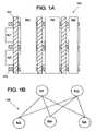
- FIG. 1illustrates metal layers that can be used by an ASIC router as represented by edges and nodes.
- FIG. 1is shown in two views, FIG. 1A shows the metal layers themselves and FIG. 1B shows a representation using nodes and connections between nodes.
- FIG. 2illustrates the use of metal to connect two points as might be done by an ASIC router.
- FIG. 3illustrates how connections can be made using two fixed layers and one configurable metal layer of a structured ASIC.
- FIG. 3is presented in three views.
- FIG. 3Ashows a layer with only horizontal wires visible
- FIG. 3Bshows the layer with only vertical wires visible
- FIG. 3Cshows both horizontal and vertical layers.
- FIG. 4shows how a signal can traverse a cell in an ASIC using the metal configuration shown in FIG. 3 .
- FIG. 5shows a completed two-port net in an ASIC using the metal configuration shown in FIG. 3
- FIG. 6is a flowchart illustrating a process according to example embodiments of the invention.
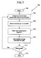
- FIG. 7is another flowchart illustrating another process according to example embodiments of the invention.
- FIG. 8illustrates how metal features can be ANDed together to determine where vias can be placed according to some example embodiments of the invention.
- FIG. 8is shown in two views where FIG. 8A illustrates the metal traces and FIG. 8B illustrates where vias can be placed.
- FIG. 9illustrates an example of routing channels used by a global router.
- FIG. 10shows the structure of an ASIC in which fixed wires are connected with vias to wires using configurable metal.
- FIG. 10is shown in two views, where FIG. 10A shows the physical structure of the ASIC and FIG. 10B shows how the structure can be represented graphically using nodes.
- FIG. 11is another flowchart illustrating a process according to example embodiments of the invention.
- FIG. 12is a block diagram of an instruction execution system or computing platform that can be used to implement an embodiment of the invention.
- a routing graph as discussed hereinis typically a data structure used by an ASIC router to represent portions of metal that can be used by the router.
- a routing graphfor example, blank areas on a layer can be represented by nodes and edges can be defined between blank areas that overlap, and can thus be connected by vias.
- the router in such a constructcan be used to find a minimum distance path through the routing graph to connect two points.
- FIG. 1further illustrates the above concepts.
- FIG. 1Adepicts a section, 100 , of a structured ASIC and shows metal-1 layer, 102 , and metal-2 layer, 104 . Blank areas that correspond to nodes are labeled N 1 and N 2 for metal-1 and N 3 , N 4 , and N 5 for metal-2. These areas are available for use by a router like that disclosed via specific example embodiments of the invention.
- FIG. 1Bshows a routing graph, 150 , that illustrates how these nodes are interconnected.
- FIG. 2illustrates a portion, 200 , of the metal layers of s structured ASIC that is identical to that illustrated in FIG. 1 , except that a connection between point P 1 and point P 2 have been routed.
- P 1 and P 2are both in metal-1 layer 201 .
- vias 204 and 206are used.
- FIGS. 3 , 4 , and 5depict how signals can be inter-connected using both fixed metal layers and a configurable via layer in embodiments of the invention.
- metal-3 and metal-4 layersare used as routing layers, and that the via-layer in between (via-3) is used to configure the signal paths.
- FIG. 3illustrates how wires run on the metal-3 and metal-4 layers of an example structured ASIC.
- FIG. 3Ais a metal-3 plot, 300 showing horizontal wires in even cells 302 , and vertical wires in odd cells 304 . Notice that there are some short wires that do not extend to the edges of the even cells.
- FIG. 3Bis a metal-4 plot, 330 , showing the vertical wires in even cells 332 , and horizontal wires in odd cells 334 .
- FIG. 3Cshows a plot, 360 , of the super-position of the layers depicted in FIG. 3A and FIG. 3B .
- FIG. 4shows how a user signal 400 is capable of traversing an even cell in metal-3, with section 402 , and can then use a via-3 via, 404 , to connect to metal-4, and continue horizontally through an odd cell with section 406 in the example structured ASIC depicted in FIG. 3 .
- This alternating layer patternallows the signal to traverse horizontally until a turn is desired. In this example, any time the horizontal signal crosses a vertical wire, there is a location that could have been used to connect the signal to a vertical routing track.
- FIG. 5shows a completed two-port net, 500 , in the example structured ASIC of FIG. 3 .
- this signalis connected using nothing but fixed metal-3 and metal-4 wires, and configurable via-3 vias.
- Wire sections 502 , 504 , 506 , and 508are on metal-3.
- Section 506is one of the ports.
- Wire sections 510 , 512 , 514 , and 516are on metal-4 and section 510 is the other port.
- Vias 518 , 520 , 522 , 524 , and 526are configured on via-3 to make the connections needed to complete the net.
- a routing graph extractordetermines the fixed wires on the fixed layers of metal, and creates nodes for these. Edges are created between wires to represent when it is possible to short two wires using a configurable layer of metal, such as a via layer. Note that a wire can span multiple layers, so long as fixed vias can be used to connect all the traces that make up the wire.
- FIG. 6is a flowchart that illustrates how a routing graph can be extracted according to some embodiments of the invention.
- FIG. 6presents process 600 of extracting the routing graph as a series of process blocks.
- the physical layout of the structured ASICis examined.
- nodesare formed to represent at least the fixed metal traces, wires, or areas of the ASIC. Note that in some embodiments, nodes can also be used to represent configurable metal.
- edgesare created representing connection opportunities between layers. These connection opportunities can be provided in various ways, depending on the chip architecture and design philosophy that applies to the particular structured ASIC.
- a routing graph for the structured ASIC of interestis formed at block 608 , and is typically stored in a technology file.
- the structured ASICis then routed using the routing graph to produce a design for a finished, customized device at block 610 .
- a further routing graphcan be extracted. This option will be discussed in detail with respect to FIGS. 9 , 10 , and 11 .
- FIG. 7is a flowchart illustrating the detection and/or creation of edges when vias are used to short wires on two different layers. Again, this flowchart is shown as a series of process blocks.
- Process 700begins at block 702 .
- two layers with an intervening via layerare selected from the ASIC design.
- all of the features on the two layers of interestare mathematically shrunk by an amount corresponding to approximately one half of a via width.
- Via detectionis then accomplished at block 708 by logically ANDing the fixed metal features on the two layers adjacent to the via layer together. The resulting, virtual, ANDed layer will contain features only where metal is present on both of the other layers.
- each location where a connection is possiblebecomes an edge in the routing graph.
- a checkis made to see if there are more layers to be processed. For example, more layers might need to be processed if the particular design contains more than two metal layers with multiple intervening, configurable via layers. If more processing is required, processing branches back to block 704 . Otherwise, the process ends at block 714 .
- FIG. 8provides a graphical, “see-through” depiction of ANDed physical layers of a section 800 of an example structured ASIC.
- FIG. 8Ashows features 801 and 802 of fixed metal-3 and intersecting features 804 of fixed metal-4 layer the ASIC. Note that metal trace features 802 are longer than features 801 , but this will have no effect on the ANDed result.
- FIG. 8Bshows points 806 that represent the logical ANDing of the features of FIG. 8A .
- FIG. 9shows a schematic representation of a portion, 900 , of a structured ASIC and an example of routing channels 902 , 904 , and 906 used by a global router, and detailed path 910 for a signal chosen within the selecting routing channels.
- the signalis routed from point P 1 to point P 2 .
- Routing graphs representing fixed metalcan be combined with traditional routing graphs as well.
- Fixed wirescorrespond to nodes on fixed metal layers, while empty spaces available for routing correspond to nodes on configurable layers of metal.
- edgescan be added to the routing graph to represent these nodes.
- FIG. 10illustrates a structured ASIC and a global routing graph.
- FIG. 10Aillustrates a portion 1000 of a structured ASIC.
- FIG. 10Ais shown as if one is looking up from the substrate in order to better reveal the specific structure—the opposite of typical convention and the other Figures shown herein, which show devices as if one was looking down through the device with each higher numbered layer appearing on top of a lower numbered layer and the substrate below all the other layers.
- fixed metal wires 1002 on fixed metal-3are shorted with configurable vias to configurable metal features 1004 on configurable metal-4.
- routing graph nodes corresponding to metal-4are created to represent the available space, and nodes corresponding to metal-3 are created to represent groups of similar wires.
- Nodes N 1 and N 2are free metal nodes on metal-4, and nodes N 3 , N 4 , and N 5 are nodes representing multiple wires each on metal-3.
- the physical positions of wires in N 3 , N 4 , and N 5are not contiguous, but these wires can be grouped together nonetheless because they have similar electrical connectivity.
- FIG. 10Bshows the resulting global-routing graph, 1006 , for the ASIC illustrated in FIG. 10A .
- wires in N 4are not only all substantially identical to each other, but they are substantially identical to all the wires in N 5 . Also all the wires in N 4 are substantially identical to each other. Thus, there are only two master wires required to represent the entire fixed portion of the routing graph in the example of FIG. 10 .
- N 4 and N 5are substantially identical. They are simply instantiated in different locations.
- the routing bundles N 4 and N 5can be defined by a common master bundle, which describes the relative locations of wires within a bundle.
- All of this processing of the layout of a structured ASIC in order to create a routing graphcan take a lot of memory and run-time. Thus, in some embodiments, these steps are performed only once for each structured ASIC base, and the resulting routing graph and any needed wire or bundle definitions are saved in a technology file for later use by the router. Users of the structured ASIC can then simply load the technology file, and skip the extraction step.
- FIG. 11illustrates an example process, 1100 , for extracting a global routing graph, at least in part by using master wires and/or bundles.
- a detailed routing graph, 1102serves as the input to process 1100 .
- fixed metal wiresare examined to make determinations based on their connectivity and conductivity.
- a determinationis made as to whether a new master wire type is needed. If so, a new mater wire type is defined at block 1108 , and processing returns back to block 1104 . If not, the wire currently under consideration is associated with an existing master wire definition at block 1110 .
- another determinationis made, this time as to whether additional wires need to be examined. If so, processing again branches back to block 1104 . Otherwise, processing continues so that connectivity can be dealt with.
- bundles representing connectivity to nodesare created. This can optionally be accomplished at least in part by defining master bundles.
- electrical characteristics of wirescan be extracted at block 1116 . These can include, for example, but are not limited to, capacitance, resistance, and inductance.
- the global routing graph and the extracted electrical characteristicsare stored in a technology file for use by a router, and at block 1120 the process ends.
- FIG. 12illustrates an instruction execution system, workstation, or personal computer system that is programmed with application software to implement the preprocess design functions according to embodiments of the invention. Such a system can also manage media used to store technology files, or network connections used to exchange such files.
- System bus 1201interconnects the major components.
- the systemis controlled by processor 1202 , which serves as the central processing unit (CPU) for the system.
- System memory 1205is typically divided into multiple types of memory or memory areas such as read-only memory (ROM), and random access memory (RAM).
- ROMread-only memory
- RAMrandom access memory
- a plurality of standard input/output (I/O) adapters or devices, 1206is present.
- a typical systemcan have any number of such devices; only four are shown for clarity.
- This driveaccepts writable and read-only optical disks such as compact discs (CD's) and digital versatile discs (DVD's) as shown at 1209 .
- CD'scompact discs
- DVD'sdigital versatile discs
- a workstation implementing all or a portion of the inventionmay contain an I/O device in the form of a network or local area network (LAN) communications (COM) adapter, 1211 , to connect to network 1212 .
- the networkcan be used to transfer software implementing the invention, or to share design files.
- a display, 1215is also connected, as well as a keyboard, 1216 .
- Any of the adaptersshould be thought of as functional elements more so than discrete pieces of hardware.
- a workstation or personal computercould have all or some of the adapter entities implemented on one circuit board. It should be noted that the system of FIG. 12 is meant as an illustrative example only. Numerous types of general-purpose computer systems and workstations are available and can be used. Available systems include those that run operating systems such as WindowsTM by Microsoft, various versions of Linux, and various versions of Unix, such as those implemented by the IBM Corporation, Sun Microsystems, Inc., and Apple Computer, Inc.
- Computer program elements of the inventionmay be embodied in hardware and/or in software (including firmware, resident software, micro-code, etc.).
- the inventionmay take the form of a computer program product, which can be embodied by a computer-usable or computer-readable storage medium having computer-usable or computer-readable, program instructions or “code” embodied in the medium for use by or in connection with the instruction execution system.
- Such mediumsare pictured in FIG. 12 to represent the optical disc, and the fixed disc.
- a computer-usable or computer-readable mediummay be any medium that can contain, store, communicate, propagate, or transport the program for use by or in connection with the instruction execution system, apparatus, or device.
- the computer-usable or computer-readable mediummay be, for example but not limited to, an electronic, magnetic, optical, electromagnetic, infrared, or semiconductor system, apparatus, device, or propagation medium such as the Internet.
- the computer-usable or computer-readable mediumcould even be paper or another suitable medium upon which the program is printed, as the program can be electronically captured, via, for instance, optical scanning of the paper or other medium, then compiled, interpreted, or otherwise processed in a suitable manner.
- the computer program product and the hardware described in FIG. 12can form the various means for carrying out the functions in some of the example embodiments.
Landscapes
- Engineering & Computer Science (AREA)
- Computer Hardware Design (AREA)
- Physics & Mathematics (AREA)
- Theoretical Computer Science (AREA)
- Evolutionary Computation (AREA)
- Geometry (AREA)
- General Engineering & Computer Science (AREA)
- General Physics & Mathematics (AREA)
- Design And Manufacture Of Integrated Circuits (AREA)
Abstract
Description
Claims (26)
Priority Applications (1)
| Application Number | Priority Date | Filing Date | Title |
|---|---|---|---|
| US10/904,411US7334208B1 (en) | 2004-11-09 | 2004-11-09 | Customization of structured ASIC devices using pre-process extraction of routing information |
Applications Claiming Priority (1)
| Application Number | Priority Date | Filing Date | Title |
|---|---|---|---|
| US10/904,411US7334208B1 (en) | 2004-11-09 | 2004-11-09 | Customization of structured ASIC devices using pre-process extraction of routing information |
Publications (1)
| Publication Number | Publication Date |
|---|---|
| US7334208B1true US7334208B1 (en) | 2008-02-19 |
Family
ID=39059600
Family Applications (1)
| Application Number | Title | Priority Date | Filing Date |
|---|---|---|---|
| US10/904,411Expired - LifetimeUS7334208B1 (en) | 2004-11-09 | 2004-11-09 | Customization of structured ASIC devices using pre-process extraction of routing information |
Country Status (1)
| Country | Link |
|---|---|
| US (1) | US7334208B1 (en) |
Cited By (8)
| Publication number | Priority date | Publication date | Assignee | Title |
|---|---|---|---|---|
| US20070294659A1 (en)* | 2005-04-01 | 2007-12-20 | Altera Corporation | Methods for producing equivalent field-programmable gate arrays and structured application-specific integrated circuits |
| US20090065813A1 (en)* | 2007-09-06 | 2009-03-12 | Viasic, Inc. | Configuring structured asic fabric using two non-adjacent via layers |
| US20130009666A1 (en)* | 2007-08-20 | 2013-01-10 | Altera Corporation | Field programmable gate array with integrated application specific integrated circuit fabric |
| US8866306B2 (en) | 2013-01-02 | 2014-10-21 | International Business Machines Corporation | Signal path and method of manufacturing a multiple-patterned semiconductor device |
| US9021407B2 (en)* | 2013-01-02 | 2015-04-28 | International Business Machines Corporation | Signal path of a multiple-patterned semiconductor device |
| US9087879B2 (en) | 2013-07-02 | 2015-07-21 | International Business Machines Corporation | Method of making semiconductor device with distinct multiple-patterned conductive tracks on a same level |
| US10127343B2 (en)* | 2014-12-11 | 2018-11-13 | Mentor Graphics Corporation | Circuit design layout in multiple synchronous representations |
| US10140410B1 (en)* | 2016-11-11 | 2018-11-27 | Cadence Design Systems, Inc. | Representing a routing strip in an integrated circuit design using a digit pattern |
Citations (55)
| Publication number | Priority date | Publication date | Assignee | Title |
|---|---|---|---|---|
| US4641108A (en) | 1985-10-16 | 1987-02-03 | Raytheon Company | Configurable analog integrated circuit |
| US4713792A (en) | 1985-06-06 | 1987-12-15 | Altera Corporation | Programmable macrocell using eprom or eeprom transistors for architecture control in programmable logic circuits |
| US4734654A (en) | 1986-08-19 | 1988-03-29 | Regents Of The University Of Minnesota | Linear CMOS transconductance element |
| US4760349A (en) | 1986-08-19 | 1988-07-26 | Regents Of The University Of Minnesota | CMOS analog standard cell arrays using linear transconductance elements |
| US5068603A (en) | 1987-10-07 | 1991-11-26 | Xilinx, Inc. | Structure and method for producing mask-programmed integrated circuits which are pin compatible substitutes for memory-configured logic arrays |
| EP0491567A1 (en) | 1990-12-19 | 1992-06-24 | Honeywell Inc. | Integrated sensor assembly |
| EP0499383A2 (en) | 1991-02-13 | 1992-08-19 | Actel Corporation | Mixed mode analog/digital programmable interconnect architecture |
| US5317919A (en) | 1992-06-16 | 1994-06-07 | Teledyne Industries, Inc. | A precision capacitor sensor |
| US5367430A (en) | 1992-10-21 | 1994-11-22 | Presidio Components, Inc. | Monolithic multiple capacitor |
| US5404265A (en) | 1992-08-28 | 1995-04-04 | Fujitsu Limited | Interconnect capacitors |
| US5459634A (en) | 1989-05-15 | 1995-10-17 | Rogers Corporation | Area array interconnect device and method of manufacture thereof |
| US5517040A (en) | 1987-04-30 | 1996-05-14 | International Business Machines Corporation | Personalizable semiconductor chips for analog and analog/digital circuits |
| US5590016A (en) | 1993-12-16 | 1996-12-31 | Tdk Corporation | Multilayer through type capacitor array |
| US5815004A (en) | 1995-10-16 | 1998-09-29 | Xilinx, Inc. | Multi-buffered configurable logic block output lines in a field programmable gate array |
| US5815726A (en) | 1994-11-04 | 1998-09-29 | Altera Corporation | Coarse-grained look-up table architecture |
| US5821776A (en) | 1997-01-31 | 1998-10-13 | Actel Corporation | Field programmable gate array with mask programmed analog function circuits |
| US5825202A (en) | 1996-09-26 | 1998-10-20 | Xilinx, Inc. | Integrated circuit with field programmable and application specific logic areas |
| US5874834A (en) | 1997-03-04 | 1999-02-23 | Xilinx, Inc. | Field programmable gate array with distributed gate-array functionality |
| US5883423A (en) | 1996-02-23 | 1999-03-16 | National Semiconductor Corporation | Decoupling capacitor for integrated circuit signal driver |
| US5898318A (en) | 1994-11-04 | 1999-04-27 | Altera Corporation | Programmable logic array integrated circuits with enhanced cascade |
| US5905385A (en) | 1997-04-01 | 1999-05-18 | Advanced Micro Devices, Inc. | Memory bits used to couple look up table inputs to facilitate increased availability to routing resources particularly for variable sized look up tables for a field programmable gate array (FPGA) |
| US5999015A (en) | 1997-02-20 | 1999-12-07 | Altera Corporation | Logic region resources for programmable logic devices |
| US6014038A (en) | 1997-03-21 | 2000-01-11 | Lightspeed Semiconductor Corporation | Function block architecture for gate array |
| US6020755A (en) | 1997-09-26 | 2000-02-01 | Lucent Technologies Inc. | Hybrid programmable gate arrays |
| US6150837A (en) | 1997-02-28 | 2000-11-21 | Actel Corporation | Enhanced field programmable gate array |
| US6166403A (en) | 1997-11-12 | 2000-12-26 | Lsi Logic Corporation | Integrated circuit having embedded memory with electromagnetic shield |
| US6184707B1 (en) | 1998-10-07 | 2001-02-06 | Altera Corporation | Look-up table based logic element with complete permutability of the inputs to the secondary signals |
| US6194912B1 (en) | 1999-03-11 | 2001-02-27 | Easic Corporation | Integrated circuit device |
| US6236229B1 (en) | 1999-05-13 | 2001-05-22 | Easic Corporation | Integrated circuits which employ look up tables to provide highly efficient logic cells and logic functionalities |
| US6242767B1 (en) | 1997-11-10 | 2001-06-05 | Lightspeed Semiconductor Corp. | Asic routing architecture |
| US6245634B1 (en) | 1999-10-28 | 2001-06-12 | Easic Corporation | Method for design and manufacture of semiconductors |
| US6278148B1 (en) | 1997-03-19 | 2001-08-21 | Hitachi, Ltd. | Semiconductor device having a shielding conductor |
| US6294927B1 (en) | 2000-06-16 | 2001-09-25 | Chip Express (Israel) Ltd | Configurable cell for customizable logic array device |
| US6331790B1 (en) | 2000-03-10 | 2001-12-18 | Easic Corporation | Customizable and programmable cell array |
| US6331733B1 (en) | 1999-08-10 | 2001-12-18 | Easic Corporation | Semiconductor device |
| US6411494B1 (en) | 2000-04-06 | 2002-06-25 | Gennum Corporation | Distributed capacitor |
| US20020085334A1 (en) | 2000-12-29 | 2002-07-04 | Intel Corporation | Multiple tier array capacitor and methods of fabrication therefor |
| US20020084509A1 (en) | 2001-01-02 | 2002-07-04 | International Business Machines Corporation | Spiral inductor semiconducting device with grounding strips and conducting vias |
| US6467074B1 (en) | 2000-03-21 | 2002-10-15 | Ammocore Technology, Inc. | Integrated circuit architecture with standard blocks |
| US6476695B1 (en) | 1999-05-26 | 2002-11-05 | Sharp Kabushiki Kaisha | High frequency module |
| US6492833B1 (en) | 1998-04-30 | 2002-12-10 | Altera Corporation | Configurable memory design for masked programmable logic |
| US20020186045A1 (en) | 2001-06-08 | 2002-12-12 | Cox William D. | Cell architecture to reduce customization in a semiconductor device |
| US6507216B1 (en) | 1998-11-18 | 2003-01-14 | Altera Corporation | Efficient arrangement of interconnection resources on programmable logic devices |
| US6588005B1 (en) | 1998-12-11 | 2003-07-01 | Hitachi, Ltd. | Method of manufacturing semiconductor integrated circuit device |
| US6614645B1 (en) | 2002-11-12 | 2003-09-02 | National Semiconductor Corporation | Matched capacitor array |
| US6646323B2 (en) | 2001-05-04 | 2003-11-11 | Texas Instruments Incorporated | Zero mask high density metal/insulator/metal capacitor |
| US6646860B2 (en) | 2001-10-30 | 2003-11-11 | Fujitsu Limited | Capacitor and method for fabricating the same |
| US20040004241A1 (en) | 2000-08-31 | 2004-01-08 | Texas Instruments Incorporated | On-chip capacitor |
| US6684173B2 (en) | 2001-10-09 | 2004-01-27 | Micron Technology, Inc. | System and method of testing non-volatile memory cells |
| US6693454B2 (en) | 2002-05-17 | 2004-02-17 | Viasic, Inc. | Distributed RAM in a logic array |
| US6696856B1 (en) | 2001-10-30 | 2004-02-24 | Lightspeed Semiconductor Corporation | Function block architecture with variable drive strengths |
| US20040129966A1 (en) | 2002-10-29 | 2004-07-08 | Horia Giuroiu | Metal-metal capacitor array |
| US6873185B2 (en) | 2002-06-19 | 2005-03-29 | Viasic, Inc. | Logic array devices having complex macro-cell architecture and methods facilitating use of same |
| US6938234B1 (en)* | 2002-01-22 | 2005-08-30 | Cadence Design Systems, Inc. | Method and apparatus for defining vias |
| US7089524B1 (en)* | 2002-01-22 | 2006-08-08 | Cadence Design Systems, Inc. | Topological vias route wherein the topological via does not have a coordinate within the region |
- 2004
- 2004-11-09USUS10/904,411patent/US7334208B1/ennot_activeExpired - Lifetime
Patent Citations (59)
| Publication number | Priority date | Publication date | Assignee | Title |
|---|---|---|---|---|
| US4713792A (en) | 1985-06-06 | 1987-12-15 | Altera Corporation | Programmable macrocell using eprom or eeprom transistors for architecture control in programmable logic circuits |
| US4641108A (en) | 1985-10-16 | 1987-02-03 | Raytheon Company | Configurable analog integrated circuit |
| US4734654A (en) | 1986-08-19 | 1988-03-29 | Regents Of The University Of Minnesota | Linear CMOS transconductance element |
| US4760349A (en) | 1986-08-19 | 1988-07-26 | Regents Of The University Of Minnesota | CMOS analog standard cell arrays using linear transconductance elements |
| US5517040A (en) | 1987-04-30 | 1996-05-14 | International Business Machines Corporation | Personalizable semiconductor chips for analog and analog/digital circuits |
| US5068603A (en) | 1987-10-07 | 1991-11-26 | Xilinx, Inc. | Structure and method for producing mask-programmed integrated circuits which are pin compatible substitutes for memory-configured logic arrays |
| US5459634A (en) | 1989-05-15 | 1995-10-17 | Rogers Corporation | Area array interconnect device and method of manufacture thereof |
| EP0491567A1 (en) | 1990-12-19 | 1992-06-24 | Honeywell Inc. | Integrated sensor assembly |
| EP0499383A2 (en) | 1991-02-13 | 1992-08-19 | Actel Corporation | Mixed mode analog/digital programmable interconnect architecture |
| US5317919A (en) | 1992-06-16 | 1994-06-07 | Teledyne Industries, Inc. | A precision capacitor sensor |
| US5404265A (en) | 1992-08-28 | 1995-04-04 | Fujitsu Limited | Interconnect capacitors |
| US5367430A (en) | 1992-10-21 | 1994-11-22 | Presidio Components, Inc. | Monolithic multiple capacitor |
| US5590016A (en) | 1993-12-16 | 1996-12-31 | Tdk Corporation | Multilayer through type capacitor array |
| US5815726A (en) | 1994-11-04 | 1998-09-29 | Altera Corporation | Coarse-grained look-up table architecture |
| US5898318A (en) | 1994-11-04 | 1999-04-27 | Altera Corporation | Programmable logic array integrated circuits with enhanced cascade |
| US5815004A (en) | 1995-10-16 | 1998-09-29 | Xilinx, Inc. | Multi-buffered configurable logic block output lines in a field programmable gate array |
| US5883423A (en) | 1996-02-23 | 1999-03-16 | National Semiconductor Corporation | Decoupling capacitor for integrated circuit signal driver |
| US5825202A (en) | 1996-09-26 | 1998-10-20 | Xilinx, Inc. | Integrated circuit with field programmable and application specific logic areas |
| US5821776A (en) | 1997-01-31 | 1998-10-13 | Actel Corporation | Field programmable gate array with mask programmed analog function circuits |
| US5999015A (en) | 1997-02-20 | 1999-12-07 | Altera Corporation | Logic region resources for programmable logic devices |
| US6150837A (en) | 1997-02-28 | 2000-11-21 | Actel Corporation | Enhanced field programmable gate array |
| US5874834A (en) | 1997-03-04 | 1999-02-23 | Xilinx, Inc. | Field programmable gate array with distributed gate-array functionality |
| US6278148B1 (en) | 1997-03-19 | 2001-08-21 | Hitachi, Ltd. | Semiconductor device having a shielding conductor |
| US6014038A (en) | 1997-03-21 | 2000-01-11 | Lightspeed Semiconductor Corporation | Function block architecture for gate array |
| US5905385A (en) | 1997-04-01 | 1999-05-18 | Advanced Micro Devices, Inc. | Memory bits used to couple look up table inputs to facilitate increased availability to routing resources particularly for variable sized look up tables for a field programmable gate array (FPGA) |
| US6020755A (en) | 1997-09-26 | 2000-02-01 | Lucent Technologies Inc. | Hybrid programmable gate arrays |
| US6242767B1 (en) | 1997-11-10 | 2001-06-05 | Lightspeed Semiconductor Corp. | Asic routing architecture |
| US6166403A (en) | 1997-11-12 | 2000-12-26 | Lsi Logic Corporation | Integrated circuit having embedded memory with electromagnetic shield |
| US6492833B1 (en) | 1998-04-30 | 2002-12-10 | Altera Corporation | Configurable memory design for masked programmable logic |
| US6184707B1 (en) | 1998-10-07 | 2001-02-06 | Altera Corporation | Look-up table based logic element with complete permutability of the inputs to the secondary signals |
| US6507216B1 (en) | 1998-11-18 | 2003-01-14 | Altera Corporation | Efficient arrangement of interconnection resources on programmable logic devices |
| US6588005B1 (en) | 1998-12-11 | 2003-07-01 | Hitachi, Ltd. | Method of manufacturing semiconductor integrated circuit device |
| US6194912B1 (en) | 1999-03-11 | 2001-02-27 | Easic Corporation | Integrated circuit device |
| US6236229B1 (en) | 1999-05-13 | 2001-05-22 | Easic Corporation | Integrated circuits which employ look up tables to provide highly efficient logic cells and logic functionalities |
| US6331789B2 (en) | 1999-05-13 | 2001-12-18 | Easic Corporation | Semiconductor device |
| US6476695B1 (en) | 1999-05-26 | 2002-11-05 | Sharp Kabushiki Kaisha | High frequency module |
| US6331733B1 (en) | 1999-08-10 | 2001-12-18 | Easic Corporation | Semiconductor device |
| US6245634B1 (en) | 1999-10-28 | 2001-06-12 | Easic Corporation | Method for design and manufacture of semiconductors |
| US6331790B1 (en) | 2000-03-10 | 2001-12-18 | Easic Corporation | Customizable and programmable cell array |
| US6467074B1 (en) | 2000-03-21 | 2002-10-15 | Ammocore Technology, Inc. | Integrated circuit architecture with standard blocks |
| US6411494B1 (en) | 2000-04-06 | 2002-06-25 | Gennum Corporation | Distributed capacitor |
| US20040027156A1 (en) | 2000-06-16 | 2004-02-12 | Lior Amarilio | Configurable cell for customizable logic array device |
| US6294927B1 (en) | 2000-06-16 | 2001-09-25 | Chip Express (Israel) Ltd | Configurable cell for customizable logic array device |
| US20040004241A1 (en) | 2000-08-31 | 2004-01-08 | Texas Instruments Incorporated | On-chip capacitor |
| US20020085334A1 (en) | 2000-12-29 | 2002-07-04 | Intel Corporation | Multiple tier array capacitor and methods of fabrication therefor |
| US20020084509A1 (en) | 2001-01-02 | 2002-07-04 | International Business Machines Corporation | Spiral inductor semiconducting device with grounding strips and conducting vias |
| US6646323B2 (en) | 2001-05-04 | 2003-11-11 | Texas Instruments Incorporated | Zero mask high density metal/insulator/metal capacitor |
| US6580289B2 (en) | 2001-06-08 | 2003-06-17 | Viasic, Inc. | Cell architecture to reduce customization in a semiconductor device |
| US20020186045A1 (en) | 2001-06-08 | 2002-12-12 | Cox William D. | Cell architecture to reduce customization in a semiconductor device |
| US6684173B2 (en) | 2001-10-09 | 2004-01-27 | Micron Technology, Inc. | System and method of testing non-volatile memory cells |
| US6646860B2 (en) | 2001-10-30 | 2003-11-11 | Fujitsu Limited | Capacitor and method for fabricating the same |
| US6696856B1 (en) | 2001-10-30 | 2004-02-24 | Lightspeed Semiconductor Corporation | Function block architecture with variable drive strengths |
| US6938234B1 (en)* | 2002-01-22 | 2005-08-30 | Cadence Design Systems, Inc. | Method and apparatus for defining vias |
| US7089524B1 (en)* | 2002-01-22 | 2006-08-08 | Cadence Design Systems, Inc. | Topological vias route wherein the topological via does not have a coordinate within the region |
| US6693454B2 (en) | 2002-05-17 | 2004-02-17 | Viasic, Inc. | Distributed RAM in a logic array |
| US6873185B2 (en) | 2002-06-19 | 2005-03-29 | Viasic, Inc. | Logic array devices having complex macro-cell architecture and methods facilitating use of same |
| US20040129966A1 (en) | 2002-10-29 | 2004-07-08 | Horia Giuroiu | Metal-metal capacitor array |
| US6982454B2 (en) | 2002-10-29 | 2006-01-03 | Oki Electric Industry Co., Ltd. | Metal-metal capacitor array |
| US6614645B1 (en) | 2002-11-12 | 2003-09-02 | National Semiconductor Corporation | Matched capacitor array |
Non-Patent Citations (6)
| Title |
|---|
| "International Preliminary Examination Report" (European Patent Office), in Triad Semiconductor, Inc. International Patent Application Serial No. PCT/US2005/005836, Jul. 14, 2006. |
| "International Preliminary Examination Report" (European Patent Office), in Triad Semiconductor, Inc. International Patent Application Serial No. PCT/US2005/011361, Jul. 6, 2006. |
| "International Search Report" (European Patent Office), in Triad Semiconductor, Inc. International Patent Application Serial No. PCT/US2005/005836, Aug. 1, 2005. |
| "International Search Report" (European Patent Office), in Triad Semiconductor, Inc. International Patent Application Serial No. PCT/US2005/011361, Aug. 5, 2005. |
| "Written Opinion of the International Search Authority" (European Patent Office), in Triad Semiconductor, Inc. International Patent Application Serial No. PCT/US2005/005836. Aug. 1, 2005. |
| "Written Opinion of the International Search Authority" (European Patent Office), in Triad Semiconductor, Inc. International Patent Application Serial No. PCT/US2005/011361, Aug. 5, 2005. |
Cited By (15)
| Publication number | Priority date | Publication date | Assignee | Title |
|---|---|---|---|---|
| US20070294659A1 (en)* | 2005-04-01 | 2007-12-20 | Altera Corporation | Methods for producing equivalent field-programmable gate arrays and structured application-specific integrated circuits |
| US7877721B2 (en)* | 2005-04-01 | 2011-01-25 | Altera Corporation | Methods for producing equivalent field-programmable gate arrays and structured application-specific integrated circuits |
| US20130009666A1 (en)* | 2007-08-20 | 2013-01-10 | Altera Corporation | Field programmable gate array with integrated application specific integrated circuit fabric |
| US9705506B2 (en)* | 2007-08-20 | 2017-07-11 | Altera Corporation | Field programmable gate array with integrated application specific integrated circuit fabric |
| US20090065813A1 (en)* | 2007-09-06 | 2009-03-12 | Viasic, Inc. | Configuring structured asic fabric using two non-adjacent via layers |
| US7692309B2 (en) | 2007-09-06 | 2010-04-06 | Viasic, Inc. | Configuring structured ASIC fabric using two non-adjacent via layers |
| US9021407B2 (en)* | 2013-01-02 | 2015-04-28 | International Business Machines Corporation | Signal path of a multiple-patterned semiconductor device |
| US9082624B2 (en)* | 2013-01-02 | 2015-07-14 | International Business Machines Corporation | Signal path of a multiple-patterned semiconductor device |
| US9093451B2 (en) | 2013-01-02 | 2015-07-28 | International Business Machines Corporation | Signal path and method of manufacturing a multiple-patterned semiconductor device |
| US9099462B2 (en) | 2013-01-02 | 2015-08-04 | International Business Machines Corporation | Signal path and method of manufacturing a multiple-patterned semiconductor device |
| US8866306B2 (en) | 2013-01-02 | 2014-10-21 | International Business Machines Corporation | Signal path and method of manufacturing a multiple-patterned semiconductor device |
| US9087879B2 (en) | 2013-07-02 | 2015-07-21 | International Business Machines Corporation | Method of making semiconductor device with distinct multiple-patterned conductive tracks on a same level |
| US9099533B2 (en) | 2013-07-02 | 2015-08-04 | International Business Machines Corporation | Semiconductor device with distinct multiple-patterned conductive tracks on a same level |
| US10127343B2 (en)* | 2014-12-11 | 2018-11-13 | Mentor Graphics Corporation | Circuit design layout in multiple synchronous representations |
| US10140410B1 (en)* | 2016-11-11 | 2018-11-27 | Cadence Design Systems, Inc. | Representing a routing strip in an integrated circuit design using a digit pattern |
Similar Documents
| Publication | Publication Date | Title |
|---|---|---|
| US11126779B2 (en) | High-speed shape-based router | |
| US10418354B2 (en) | Integrated circuit and computer-implemented method of manufacturing the same | |
| Kahng et al. | VLSI physical design: from graph partitioning to timing closure | |
| US8037441B2 (en) | Gridded-router based wiring on a non-gridded library | |
| KR20190024723A (en) | Integrated circuit design and/or fabrication | |
| EP0495887A1 (en) | Improved routing system and method for integrated circuits | |
| US11036913B2 (en) | Integrated circuit methods using single-pin imaginary devices | |
| US20180165405A1 (en) | Timing based net constraints tagging with zero wire load validation | |
| US7334208B1 (en) | Customization of structured ASIC devices using pre-process extraction of routing information | |
| WO2023163910A2 (en) | Integrated circuit with non-preferred direction curvilinear wiring | |
| US20230274066A1 (en) | Concurrently routing multiple partitions of an integrated circuit design | |
| Radhakrishnan Nair et al. | An efficient partitioning and placement based fault TSV detection in 3D-IC using deep learning approach | |
| TW201826155A (en) | Integrated circuits, computer-implemented method of manufacturing the same, and standard cell defining the same | |
| US20160203254A1 (en) | Methods for reducing congestion region in layout area of ic | |
| Torabi et al. | A fast hierarchical adaptive analog routing algorithm based on integer linear programming | |
| CN112214956B (en) | System for designing semiconductor circuits and method of operating the same | |
| Pecht et al. | Advanced routing of electronic modules | |
| Lienig et al. | Methodologies for Physical Design: Models, Styles, Tasks, and Flows | |
| US20250005251A1 (en) | Equivalent wire codes for routing nets in an integrated circuit design | |
| CN120409416A (en) | Semiconductor design method and device | |
| JPH08161389A (en) | Circuit simulating method and circuit simulator | |
| Samantam et al. | A method for the multi-net multi-pin routing problem with layer assignment | |
| Ellis-Monaghan et al. | Graph theoretical problems in next-generation chip design | |
| Hrkic | Tree optimization and synthesis techniques with applications in automated design of integrated circuits | |
| Tsai et al. | Routability optimization for crossbar-switch structured ASIC design |
Legal Events
| Date | Code | Title | Description |
|---|---|---|---|
| AS | Assignment | Owner name:VIASIC, INC., NORTH CAROLINA Free format text:ASSIGNMENT OF ASSIGNORS INTEREST;ASSIGNOR:COX, WILLIAM D.;REEL/FRAME:015345/0459 Effective date:20041108 | |
| STCF | Information on status: patent grant | Free format text:PATENTED CASE | |
| FEPP | Fee payment procedure | Free format text:PAYOR NUMBER ASSIGNED (ORIGINAL EVENT CODE: ASPN); ENTITY STATUS OF PATENT OWNER: SMALL ENTITY | |
| FPAY | Fee payment | Year of fee payment:4 | |
| AS | Assignment | Owner name:TRIAD SEMICONDUCTOR, INC., NORTH CAROLINA Free format text:ASSIGNMENT OF ASSIGNORS INTEREST;ASSIGNOR:VIASIC, INC.;REEL/FRAME:029418/0552 Effective date:20121205 | |
| FPAY | Fee payment | Year of fee payment:8 | |
| AS | Assignment | Owner name:PARTNERS FOR GROWTH IV, L.P., CALIFORNIA Free format text:SECURITY INTEREST;ASSIGNOR:TRIAD SEMICONDUCTOR, INC.;REEL/FRAME:037885/0344 Effective date:20160302 | |
| AS | Assignment | Owner name:SILICON VALLEY BANK, COLORADO Free format text:AMENDED AND RESTATED INTELLECTUAL PROPERTY SECURITY AGREEMENT;ASSIGNOR:TRIAD SEMICONDUCTOR, INC.;REEL/FRAME:038106/0300 Effective date:20160302 | |
| MAFP | Maintenance fee payment | Free format text:PAYMENT OF MAINTENANCE FEE, 12TH YR, SMALL ENTITY (ORIGINAL EVENT CODE: M2553); ENTITY STATUS OF PATENT OWNER: SMALL ENTITY Year of fee payment:12 | |
| AS | Assignment | Owner name:TRIAD SEMICONDUCTOR, INC., NORTH CAROLINA Free format text:RELEASE BY SECURED PARTY;ASSIGNOR:SILICON VALLEY BANK;REEL/FRAME:053087/0492 Effective date:20161116 | |
| AS | Assignment | Owner name:CP BF LENDING, LLC, WASHINGTON Free format text:SECURITY INTEREST;ASSIGNOR:TRIAD SEMICONDUCTOR, INC.;REEL/FRAME:053180/0379 Effective date:20200708 | |
| AS | Assignment | Owner name:TRIAD SEMICONDUCTOR, INC., NORTH CAROLINA Free format text:RELEASE BY SECURED PARTY;ASSIGNOR:PARTNERS FOR GROWTH IV, L.P.;REEL/FRAME:053187/0495 Effective date:20200708 |