US7334179B2 - Method and system for detecting and correcting errors while accessing memory devices in microprocessor systems - Google Patents
Method and system for detecting and correcting errors while accessing memory devices in microprocessor systemsDownload PDFInfo
- Publication number
- US7334179B2 US7334179B2US10/919,138US91913804AUS7334179B2US 7334179 B2US7334179 B2US 7334179B2US 91913804 AUS91913804 AUS 91913804AUS 7334179 B2US7334179 B2US 7334179B2
- Authority
- US
- United States
- Prior art keywords
- error correction
- data
- code
- correction code
- error
- Prior art date
- Legal status (The legal status is an assumption and is not a legal conclusion. Google has not performed a legal analysis and makes no representation as to the accuracy of the status listed.)
- Expired - Fee Related, expires
Links
Images


Classifications
- G—PHYSICS
- G06—COMPUTING OR CALCULATING; COUNTING
- G06F—ELECTRIC DIGITAL DATA PROCESSING
- G06F11/00—Error detection; Error correction; Monitoring
- G06F11/07—Responding to the occurrence of a fault, e.g. fault tolerance
- G06F11/08—Error detection or correction by redundancy in data representation, e.g. by using checking codes
- G06F11/10—Adding special bits or symbols to the coded information, e.g. parity check, casting out 9's or 11's
- G06F11/1008—Adding special bits or symbols to the coded information, e.g. parity check, casting out 9's or 11's in individual solid state devices
- G—PHYSICS
- G06—COMPUTING OR CALCULATING; COUNTING
- G06F—ELECTRIC DIGITAL DATA PROCESSING
- G06F11/00—Error detection; Error correction; Monitoring
- G06F11/07—Responding to the occurrence of a fault, e.g. fault tolerance
- G06F11/08—Error detection or correction by redundancy in data representation, e.g. by using checking codes
- G06F11/10—Adding special bits or symbols to the coded information, e.g. parity check, casting out 9's or 11's
- G06F11/1076—Parity data used in redundant arrays of independent storages, e.g. in RAID systems
Definitions
- Certain embodiments of the inventionrelate to processing of digitized information. More specifically, certain embodiments of the invention relate to a method and system for detecting and correcting errors while accessing memory devices in microprocessor systems.
- a flash deviceis essentially an electrically erasable programmable read only memory (EEPROM or E 2 PROM), which allow blocks of data to be programmed or erased at relatively high operating speeds.
- EEPROMelectrically erasable programmable read only memory
- a flashdiffers from an EEPROM in that a flash is generally adapted to operate on blocks of data while an EEPROM or E 2 PROM has to be erased all at once, even though the EEPROM may be programmed on a byte-by-byte basis.
- a NAND flash memoryis a non-linear addressed device requiring multiplexed input/output (I/O) pins for handling both data and commands.
- a NAND flash memory deviceis a serially interfaced device in which address, data, and control information are multiplexed on the same pins. As a result of its serial interface, the NAND flash memory device requires extensive I/O interfaces and drivers for handling the multiplexed I/O pins.
- a NAND flash memory deviceis typically accessed by block or page, thereby permitting, for example, 512 bytes of data to be written to or read from the device. Random access errors generated by physical degradation in the geometry of the NAND gates results in low reliability for NAND flash memory devices.
- a NOR flash deviceis a linear addressed device, which comprises separate address and data lines.
- a NOR flash deviceis somewhat similar to a dynamic random access memory (DRAM) device.
- DRAMdynamic random access memory
- a NOR flash memorygenerally comprises sufficient address pins that allow it to be memory mapped into a processor's address space, thereby allowing the NOR flash to be accessed like a read only memory (ROM).
- the cell structure of NAND flashis almost one-half the size of a NOR flash's cell structure and as a result, for a given die, NAND flash memory devices have a much higher packing density than NOR flash memory devices.
- NOR flash capacitiesrange from 1 megabyte (MB) to 4 MBs while NAND flash capacities range from 32 MBs to 512 MBs.
- NAND flashis cheaper than NOR flash since it utilizes much smaller die size of silicon wafer than NOR flash.
- NOR flash memory devicesalso possess less than 10% of the lifespan of NAND flash memory devices.
- NAND flash memoryis typically utilized in portable electronic devices/products that require a large storage capacity, which can store data when there is a loss of power. NAND flash memory is also utilized in these products/devices because of its low cost and low power consumption when compared with traditional NOR flash memory.
- NAND flashis widely utilized in USB storage devices, MP3 players, digital answer machines, digital recorders, various kinds of memory cards including, but not limited to, compact flash cards, SmartMedia cards, and SecureDigital (SD) cards.
- SDSecureDigital
- NAND flashmay be utilized to store digitized data such as images, audio and video.
- NAND flashpossesses the highest bit densities of the various types of flash memories, is inexpensive, and has much lower power consumption than NOR flash, it has a low reliability due to runtime bad bit and prolonged access time. Unlike NOR flash, these issues of reliability with NAND flash makes it impractical to execute the computer instructions directly from the NAND flash. Notwithstanding, manufactures of NAND flash recommend the use of error correcting technology to enhance data integrity. After using error correction technology, the bad bits can be detected and corrected, thereby making the NAND flash a more practical solution for storing computer instruction and for storing data like on a hard disk, which may be managed by a file system in order to maintain data integrity.
- error correction methodologiestypically operate on a page of data of the order of 512, 1024, 2048 bytes or larger page size. Furthermore, special logic operations such as bit manipulations are required to generate the error correction codes. Accordingly, if only software is utilized to compute and/or otherwise generate the error correction codes, then a large amount of processor cycles are required because utilizing a processor for bit manipulations may be ineffective. On the other hand, if only hardware is utilized to compute the error correction codes, then additional storage is required to store the pages of data. As the page size increases, so does the amount of memory that is required for storing the page data. For embedded system applications, for example, the additional storage may be very expensive since a large gate count is required and this makes the chip very expensive.
- Certain embodiments of the inventionmay be found in a method and system for ensuring data integrity in a data processing system. Aspects of the method may comprise monitoring when the data for a specified device is available for error correction code generation, and receiving a first indication of the specified device, a second indication of the data, and a third indication of a size of the data during the monitoring.
- a new error correction codemay be generated in hardware for the data based on the indicated size of the data and an indication may be provided to signal when generation of the new error correction code for a specified number of accesses for at least a portion of the data is complete. Detected errors may be corrected in software based on the newly generated error correction code.
- the first indicationmay be a device selection signal and the error correction code generation may be enabled or disabled via an enable signal.
- the second indicationmay be a data ready signal and the third indication may be a data size signal, which indicates a size of the data.
- the methodmay also comprise counting a specified number of accesses, which may be controlled by a page size setting.
- a page countermay be specified, which indicates bytes of data that are processed.
- the methodmay also comprise generating an interrupt when the page counter indicates that all the bytes have been processed.
- a signalmay be generated that indicates when generation of the new error correction code is complete
- Error correction code generation for the datamay be deactivated and it may be determined whether the data access is a read operation or a write operation. If the data access is a write operation, then the newly generated error correction code may be written to external memory. If the data access is a read operation, then a newly generated error correction code may be read and a stored error correction code corresponding to the read data may be read or otherwise acquired.
- the integrity of the read datamay be checked and the newly generated error correction code may be compared with a stored error correction code corresponding to the read data. It may then be determined whether the newly generated error correction code matches the stored error correction code. If the newly generated error correction code does not match the stored error correction code, then it may be determined whether the error correction code is incorrect. It may further be determined whether an error is correctable if the error correction code is not in error. If the error is correctable, the error may be corrected. In instances where the error is not correctable, the processor may report the error, for example, to an upper layer application.
- a method for ensuring data integrity in a data processing systemmay comprise generating error correction codes for data utilizing a hardware on-chip error correction code module and detecting bytes in error and bits in error via code executed by a processor. The detected bytes in error and bits in error may be corrected utilizing the code executed by the processor. The method may further comprise generating a signal by the hardware on-chip error correction code module, which indicates completion of the generation of the error correction code. The processor may be notified when generation of the error correction code is complete.
- Another embodiment of the inventionmay provide a machine-readable storage, having stored thereon, a computer program having at least one code section executable by a machine, thereby causing the machine to perform the steps as described in the various embodiments above for ensuring data integrity in a data processing system.
- aspects of the systemmay comprise an error correction code module that monitors when the data for a specified device is available for error correction code generation and receives a first indication of the specified device, a second indication of the data, and a third indication of a size of the data during the monitoring.
- the error correction code modulemay generate a new error correction code in hardware for the data based on the indicated size of the data.
- An indicationmay be provided to signal when generation of the new error correction code for a specified number of accesses for at least a portion of the data is complete.
- Code executed by a processormay correct detected errors in software based on the newly generated error correction code.
- the first indicationmay be a device selection signal and an enable signal may be utilized to enable or disable generation of the error correction code.
- the data enable signalmay enable generation of the error correction code when it is asserted and disable generation of the error correction code when it is de-asserted.
- the second indicationmay be a data ready signal and the third indication may be a data size signal, which indicates a size of the data.
- a page size settingmay be utilized to count and control a specified number of accesses.
- a page countermay be specified, which indicate bytes of data that are processed. An interrupt may be generated and sent to the processor to inform error detection and correction (EDC) code when the page counter indicates that all the bytes have been processed.
- EDCerror detection and correction
- the processormay be adapted to determine whether data access for the data is a read access or a write access.
- the processormay deactivate error correction code generation and determine whether the data access is a read operation or a write operation. If the data access is a write operation, then the newly generated error correction code may be written to external memory by the processor. If the data access is a read operation, then a newly generated error correction code may be read and a stored error correction code corresponding to the read data may be read or otherwise acquired by the processor.
- the code executed by the processormay be configured to check or verify the integrity of the read data and the newly generated error correction code may be compared with a stored error correction code corresponding to the read data. The code executed by the processor may then determine whether the newly generated error correction code matches the stored error correction code and whether the error correction code is incorrect if the newly generated error correction code does not match the stored error correction code. The code executed by the processor may then determine whether a detectable error is correctable if the error correction code is not in error. If the error is correctable, the code executed by the processor may correct the error. In instances where the error is not correctable, code executed by the processor may be adapted to report the error, for example, to an upper layer application.
- Another embodiment of the system for ensuring data integrity in a data processing systemcomprises an on-chip hardware error correction code module that generates error correction codes.
- a processormay detect bytes in error and bits in error via code executed by the processor and the processor may correct the detected bytes in error and bits in error utilizing the code executed by the processor.
- the on-chip hardware error correction code modulemay generate a signal that indicates completion of the generation of the error correction code.
- the on-chip hardware error correction code modulemay also be adapted to notify the processor when generation of the error correction code is complete.
- FIG. 1is a block diagram of an exemplary system that may be utilized for generating error correction codes, in accordance with an embodiment of the invention.
- FIG. 2is a flow chart illustrating exemplary steps that may be utilized to generate error correction codes in an error correction code module based on pages of data, in accordance with an embodiment of the invention.
- FIG. 3is a flow chart illustrating exemplary steps that may be utilized to maintain page data integrity by checking for data errors and correcting them, in accordance with an embodiment of the invention.
- FIG. 4is an exemplary timing diagram illustrating timing waveforms for error correction code computing for NAND flash, in accordance with an embodiment of the invention.
- An on-chip hardware error correction code modulemay be utilized to generate error correction codes.
- software or other type of computer codemay be utilized to detect bytes in error and/or bits in error, and the detected errors may be corrected utilizing the code, which may be executed by a processor.
- the on-chip hardware error correction code modulemay generate a signal that indicates completion of the generation of the error correction code.
- the on-chip hardware error correction code modulemay also be adapted to notify the software or other type of error correction code when generation of the error correction code is complete.
- the softwaremay read the re-generated error correction code and compare it with a stored error correction code in order to detect if any data byte or bit error exists and if so, correct the error.
- the various aspects and embodiments of the inventionmay be found in a method and system that provides an optimal balance between hardware processing and software processing operations that are utilized to generate the error correction codes, and to detect and correct any detected error.
- This optimal balance between hardware and software operationsutilizes significantly less processor cycles and the gate count and consequently the die size is significantly less than other existing systems that are utilized for generating error correction codes, and for detecting and correcting errors.
- this optimal balance between hardware and softwarewhich utilizes hardware to generate the error correction codes, and software to detect and correct errors, may result in chip implementations that are about 1/10 th the size of existing similar systems that are implemented by a standalone chip.
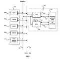
- FIG. 1is a block diagram of an exemplary system that may be utilized for generating error correction codes in accordance with an embodiment of the invention.
- a unified memory block 102there is shown a unified memory block 102 , an external memory interface (EMI) 104 , an error correction code (ECC) module or circuitry 106 , and a “processor with error detection and correction (EDC) code running on it” block 108 .
- the “processor with error detection and correction (EDC) code running on it” block 108may be referred to as the processor/EDC code 108 .
- the unified memory block 102may comprise a plurality of memory blocks, for example, NOR memory block 102 a , SRAM block 102 b , and NAND flash memory block 102 c , DRAM 102 d , and “other types of memory” block 102 e .
- the external memory interface (EMI) 104 , error correction code module 106 , and the processor 108may be integrated into a single integrated circuit (IC) chip or module. Accordingly, the NOR memory block 102 a , SRAM block 102 b , NAND flash memory block 102 c , DRAM block 102 d and “other types of memory” block 102 e may be located external to the single integrated circuit module.
- the memory block 102which may comprise NOR flash 102 a , SRAM 102 b , NAND flash 102 c , DRAM 102 d , and “other types of memory” 102 e such as SDRAM or DDR, may be integrated into a chip or module within the external memory interface module 104 , the hardware ECC module 106 and/or processor/EDC code 108 .
- the external memory interface module 104may comprise suitable logic circuitry and/or code that may be adapted to interface with the external memory modules within the unified memory block 102 , the error correction code module 106 and the processor/EDC code 108 .
- the error detection and correction codemay be adapted to instruct the EMI module 104 , through the internal bus 116 , to do read and/or write accesses to the modules within the unified memory block 102 via the address and control status bus 112 and the data bus 110 .
- the external memory interface module 104may generate one or more signals, which informs the error correction code module 106 of the corresponding data presets on the data bus and/or the data size.
- the EMI module 104may be a simple memory controller or a complex memory controller.
- a complex memory controllermay combine a memory controller with a direct memory access (DMA) controller module.
- the DMA controller modulemay initiate memory accesses like a processor does, whenever it is instructed to do so by software or other code.
- the interface between the memory controller and the DMA controller modulemay be an internal bus of module 100 , for example, bus 116 .
- the internal busmay be utilized to transfer instructions to the DMA controller module.
- the error correction code module 106comprises suitable logic or circuitry that may be adapted to generate appropriate error correction code.
- the EDC codemay be adapted to instruct the error correction code module 106 via internal bus 116 to compute error correction code, set page size and compute ECC algorithms.
- the error correction code module 106may be adapted to constantly monitor data status signal 113 and data size signal 114 and update error correction codes when the external memory interface 104 is accessing the target device such as any of the memories in the memory block 102 .
- control status bus 112 and/or data bus 110may be configured to determine which memory block within the unified memory block 102 is being accessed. Accordingly, the external memory interface 104 is adapted to generate a data status signal 113 instructing the error correction code module 106 that valid data is presently on the data bus 110 . Since the data bus 110 may be several bytes wide, the byte size signal 114 may be utilized to inform the error correction code module 106 of the size of the data in bytes that is presently on the data bus 110 . The data ready signal 113 may be utilized to signify the number of bytes of data that is presently on the bus for which error correction code should be computed. For example, the data size signal 114 my indicate that the data bus width 110 is two bytes wide and the hardware ECC module 106 may be adapted to compute the error correction code for the two bytes of data that are presently on the data bus 110 .
- the unified memory block 102permits data to be read from or written to any of the memory blocks 102 a , 102 b , 102 c , 102 d , or 102 e .
- software running on processor 108may read data from NOR memory 102 a
- softwaremay write data to SRAM 102 b
- datamay be read from or written to NAND flash memory 102 c .
- softwaremay be adapted to instruct the external memory interface 104 to access the unified memory block 102 a , 102 b , 102 c , 102 d and/or 102 e.
- the unified memorymay be accessed in a burst page mode, which means that it is continuously read or written on a per page basis, where each page contains a fixed amount of data, for example, 256, 512, 1024, bytes.
- the EDC code running on processor 108will signal the external memory interface module 104 , which will then signal the error correction code module 106 of the data access.
- the external memory interface module 104will signal the error correction code module 106 via signals 113 , 114 and 119 to initiate computation of the error code for the specified data that is presently on the bus 110 .
- signal 119may be utilized to indicate the type of memory that is being accessed. In this regard, signal 119 may be utilized by the error correction code module 106 to indicate when error correction code should be generated for a particular type of memory.
- the error correction code module 106may be adapted to compute the error correction code when the memory type indicated by signal 119 is matched with the specified memory type in the error correction code module 106 , the latter of which may be signaled by the code running on the processor 108 .
- datamay be access in any order from any of the memory blocks 102 a , 102 b , 102 c , 102 d and 102 e .
- the error correction code module 106update error correction codes. For example, error correction codes may be generated for all access to NAND block 102 c . However, accessed to NOR block 102 a may not require generation of error correction codes by the error correction code module 106 . If the error correction code 106 is instructed to compute error correction code for multiple memory devices during mixed memory page access, the error correction code module 106 may utilize one or more sets of computing units to generate the corresponding error correction codes in parallel.
- the hardware error correction code module 106may temporarily store two current error correction codes, one for each device. Accordingly, each code may be updated when there is access to its device.
- the external memory interface module 104may be adapted to utilize signal 113 to inform the error correction code module 106 that the data is presently on the data bus 110 . Furthermore, the external memory interface module 104 may utilize signal 114 to indicate the size of the data that is indicated by signal 113 .
- Signal 119indicates which memory device is being accessed. For example, signal 119 may indicate that NAND flash 102 c is being accessed. In an aspect of the invention, signal 119 may be matched with an internal device setting generated by the processor and EDC code 108 .
- the error correction code module 106uses the data on the data bus 110 to compute error correction code for every byte presented on the data bus 110 . If there are more bytes on data bus 110 and the error correction code module 106 has enough time to compute the corresponding error correction code for all bytes presently on the data bus before signal 113 again indicates the next accessed data is available on the data bus 110 , the error correction code module 106 may utilize one computing unit that computes one byte in one clock cycle. Otherwise, the error correction code module 106 may utilize more computing units to parallel compute error correction code in a given time period.
- the error correction code module 106may utilize a counter to indicate when an amount of data equivalent to the page size has been processed. Accordingly, the error correction code module 106 may utilize a signal such as interrupt signal 115 to notify the EDC code running on the processor 108 that the error correction code is ready in the error correction code module 106 . In this regard, the EDC does not need to generate the error correction code and this significantly reduces utilization of processor computing cycles. Accordingly, during error code generation, the EDC processes may be suspended, thereby allowing other programs to be executed. If the interrupt signal 115 is asserted, the EDC code may be activated and begins running.
- the error detection and correction (EDC) codemay then read the error correction code from the error correction code module 106 via bus interface 116 and determine whether to stop the error correction code module 106 from monitoring the external memory interface module 104 . Determining whether to end monitoring of the EMI 104 is done since the next data access presented on the data bus 110 may not be related to the page data that was utilized to compute the error correction code. One scenario in which this may occur is when the data is for another memory location.
- the error correction code that is generated by the error correction code module 106may be read by the EDC code and then written to the corresponding external memory page.
- This stored error correction code that is written to the corresponding external memory pagemay function as an integrity pattern for that page of data, and may subsequently be utilized to verify the integrity of the associated page of data whenever the page is read.
- the EDC code running on processor 108may compare the newly generated error correction code with an original error correction code stored in the corresponding memory block from which the page of data is read. If the error codes are inconsistent and the error cannot be corrected, the EDC code may generate an error signal or other indication of the error and the data may have to be re-read from external memory 102 . If the error is correctable based on the compared result of the two error correction codes, the EDC code may correct the error within the page of data that has already been read into an internal or main memory. An address of the error bit may be determined by comparing the two error correction codes, and the compared result may indicate which bit in a corresponding byte of the read page may be corrupted.
- the EDC code executed by the processor 108may locate the byte and correct the error bit without reading from the external memory again. Accordingly, the error correction code generation module 106 does not need to store a whole page of data in order to correct a bit in error. Since it is not necessary to store the whole page of data, the die size of the chip can be significantly reduced.
- the error correction codeis 22 bits.
- the 22 bits of error correction codescomprises 16 byte parity bits and 6 column parity bits.
- the EDC codemay be adapted to do an XOR operation between the newly generated error correction code and the error correction code that is stored in the NAND flash block 102 c .
- the EDC codeis adapted to acquire a 22-bit result in one instruction cycle. If the result of the XOR operation is equal to logic zero (0), this means that there is no error bit in the 256-byte read data page.
- the EDC codemay then get the byte address by concatenating bits 21 , 19 , 17 , 15 , 13 , 11 , 9 , and 7 of the XORed result and get the bit address in the byte by concatenating bits 5 , 3 and 1 . If only one bit in the compared result is logic one (1), this means that the stored error correction code is corrupt. In this case, the EDC code may instruct the error correction code module 106 to regenerate the error correction code by reading the same page again.
- the EDC codemay read the page data again or try other methods to recovery the read data, or just simply abandon correction.
- Exemplary error correction codemay comprise Hamming codes, Reed Solomon (RS) codes or other types of error correction codes, some of which may correct more bit errors than others. Utilizing more error correction codes for a fixed amount of page data may result in the correction of more errors.
- the EDC codemay allow the hardware ECC module 106 to monitor signals 113 , 114 and 119 after receiving an indication that generation of error correction code for the past page of data is finished.
- Sequential accessmeans that data may be read or written page by page without any inserted access intervention to handle control and/or status data on data bus 110 or access other memory or other page in the same memory. Accordingly, once the second page of data is presented on the data bus 110 , the hardware ECC module 106 may generate a second error correction code for the second page of data without any reset or refresh operation for the hardware error correction code module 106 .
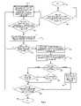
- FIG. 2is a flow chart illustrating exemplary steps that may be utilized to generate error correction codes in an error correction code module based on pages of data, in accordance with an embodiment of the invention.
- the exemplary stepsstart with step 202 .
- EDC codedetermines whether error correction code should be generated for the following page of data accessed for a specific device in 102 . If it is determined that the error correction code should not be generated for the following page of data, then step 204 is repeated.
- the EDC codemay activate the hardware ECC module 106 to monitor device selection signal 119 , the data ready signal 113 , and the data size signal 114 , and the processor/EDC 108 may set the page size and memory type setting in the hardware ECC module 106 .
- step 208it may be determined whether the data ready signal 113 and device selection signal 119 indicate that the data to generate error correction code is ready on the data bus 110 . If the data ready signal 113 indicates that data is not ready on the data bus 110 , then step 208 is repeated. If the data ready signal 113 indicates that data is ready on the data bus 110 , then in step 210 , the hardware error correction code module 106 computes error correction code for presented bytes based on data bus 110 as indicated by the data size signal 114 . In step 212 , the hardware ECC module 106 determines whether a byte counter value is equivalent to a page size setting. If the byte counter value is not equivalent to a page size setting, then control passes back to step 208 . However, if the byte counter value is equivalent to a page size setting, then in step 214 , the error correction code module 106 may generate a signal, which indicates that computing of the error correction code is complete and the EDC code may read the generated error correction code.
- the EDC codemay deactivate the hardware ECC module 106 and read the stored error correction code from the hardware ECC module 106 .
- the EDC codemay determine whether the page that is accessed is a read operation. If the page access is a read operation, then in step 222 , the EDC code may check data integrity. If the data integrity is to be checked, then the EDC code goes to step 302 of FIG. 3 . However, if it is determined that the data integrity is not to be checked, then in step 224 , the EDC code determines whether to compute the error correction code for the next continuous page data. If the error correction should be computed for the next continuous page data, then control passes back to step 206 .
- step 228if the EDC code determines that the page access is not a read operation but is instead a write operation, then in step 220 , the EDC code may write the newly generated error correction code to external memory. Step 224 is then executed.
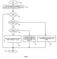
- FIG. 3is a flow chart illustrating exemplary steps that may be utilized to maintain page data integrity by checking for data errors and correcting them, in accordance with an embodiment of the invention.
- the exemplary stepsmay start with step 302 .
- Step 302may be executed in place of step 226 of FIG. 2 .
- the EDC codecompares the newly generated error correction code with a stored error correction code.
- step 306it may be determined whether there is a match between the newly generated error correction code and the stored error correction code. If there is a match, then the exemplary steps may end at step 318 . If there is no match between the newly generated error correction code and the stored error correction code, then in step 308 , it may be determined whether only the error correction code is in error.
- step 316read page data has no error and the EDC code may start the procedure to fix the problem. For example, the EDC and the EDC code relocates the page data to another memory location and a new error correction code generated during writing to the new memory location. If only the error correction code is not in error in step 308 , then in step 310 , it may be determined whether the error is correctable. If the error is correctable, then in step 312 , the EDC code may start a procedure to correct the error bit(s) within the page. If the error is not correctable in step 310 , then in step 314 , the page data error cannot be corrected and the EDC code reports the error to a higher-level application. Subsequent to steps 312 , 314 , and 316 , the exemplary steps may end with step 318 .
- FIG. 4is an exemplary timing diagram illustrating timing waveforms for error correction code computing for NAND flash, in accordance with an embodiment of the invention.
- data bus signal 110there is shown data bus signal 110 , enable error correction code signal 412 , device select signal 119 , data ready signal 113 , data size signal 114 , interrupt signal 115 and internal status for ECC generation 416 .
- the internal status for error code (ECC) generation 416is not a true signal but is utilized to indicate periods of ECC generation.
- the error correction code enable signal 412may be an internal or external signal for module 106 .
- the data bus signal 110illustrates periods of valid data and periods of invalid data.
- reference 402indicates a valid cycle for NAND flash access since device selection signal 119 is asserted during that interval.
- reference 404 aindicates an interval that is not a valid NAND flash access cycle. Data is not valid on the data bus 110 ( FIG. 1 ) during intervals 404 b and invalid 404 c .
- the error detection and correction codeasserts the error correction code enable signal 412 , this causes the error correction code module 106 of FIG. 1 to initiate monitoring of the device selection signal 119 , the data ready signal 113 and the data size signal 114 , in order to generate error correction codes based on valid data presently on data bus 110 .
- the device selection signal 119indicates when the NAND block 102 c of FIG. 1 is accessed. In this regard, whenever the device selection signal 119 is asserted, this indicates an access to the NAND block 102 c.
- generation of the error correction codemay be initiated when the enable error correction code signal 412 is asserted. While the error correction code signal 412 is asserted and data is ready on the data bus 110 as indicated by assertion of the device selection signal 119 , data ready signal 113 , the data size signal 114 indicates the size of the data for which error codes should be generated.
- the error correction code module 106may compute the error correction code for the NAND block 102 c when the device selection signal 119 is asserted during a valid data cycle such as 402 . After generation of the error correction code is complete, an indication signal such as interrupt 115 may be sent to the processor to inform the EDC code of the completion.
- Intervals 406 a , 406 cdescribe an internal status of the error correction code module 106 and illustrate intervals during which three consecutive error correction codes are computed.
- Interval 406 dillustrates when the last computation is done in a current phase, and the error correction code is generated for the past page of data.
- the inventionovercomes the drawbacks inherent in conventional systems that utilize either a dedicated software solution or a dedicated hardware solution. Notwithstanding, it should readily be understood that the invention is not limited to being utilized for NAND flash memory applications, but may be utilized for other flash memories that utilize burst data page operations like NOR flash memory to maintain data integrity with very low system performance cost and hardware cost.
- the present inventionmay be realized combination of hardware and software that the hardware takes computing intensive takes that is generating the error correction code and software that has no limitation to access page data.
- the present inventionmay be realized in a centralized fashion in at least one computer system or in a distributed fashion where different elements are spread across several interconnected computer systems. Any kind of computer system or other apparatus adapted for carrying out the methods described herein is suited.
- a typical combination of hardware and softwaremay be a general-purpose computer system with a computer program that, when being loaded and executed, controls the computer system such that it carries out the methods described herein.
- the present inventionmay also be embedded in a computer program product, which comprises all the features enabling the implementation of the methods described herein, and which when loaded in a computer system is able to carry out these methods.
- Computer program in the present contextmeans any expression, in any language, code or notation, of a set of instructions intended to cause a system having an information processing capability to perform a particular function either directly or after either or both of the following: a) conversion to another language, code or notation; b) reproduction in a different material form.
Landscapes
- Engineering & Computer Science (AREA)
- Theoretical Computer Science (AREA)
- Quality & Reliability (AREA)
- Physics & Mathematics (AREA)
- General Engineering & Computer Science (AREA)
- General Physics & Mathematics (AREA)
- Techniques For Improving Reliability Of Storages (AREA)
- Detection And Correction Of Errors (AREA)
Abstract
Description
Claims (79)
Priority Applications (2)
| Application Number | Priority Date | Filing Date | Title |
|---|---|---|---|
| US10/919,138US7334179B2 (en) | 2004-06-04 | 2004-08-16 | Method and system for detecting and correcting errors while accessing memory devices in microprocessor systems |
| US12/026,107US8335960B2 (en) | 2004-06-04 | 2008-02-05 | Method and system for detecting and correcting errors while accessing memory devices in microprocessor systems |
Applications Claiming Priority (2)
| Application Number | Priority Date | Filing Date | Title |
|---|---|---|---|
| US57700704P | 2004-06-04 | 2004-06-04 | |
| US10/919,138US7334179B2 (en) | 2004-06-04 | 2004-08-16 | Method and system for detecting and correcting errors while accessing memory devices in microprocessor systems |
Related Child Applications (1)
| Application Number | Title | Priority Date | Filing Date |
|---|---|---|---|
| US12/026,107ContinuationUS8335960B2 (en) | 2004-06-04 | 2008-02-05 | Method and system for detecting and correcting errors while accessing memory devices in microprocessor systems |
Publications (2)
| Publication Number | Publication Date |
|---|---|
| US20050283650A1 US20050283650A1 (en) | 2005-12-22 |
| US7334179B2true US7334179B2 (en) | 2008-02-19 |
Family
ID=35481955
Family Applications (2)
| Application Number | Title | Priority Date | Filing Date |
|---|---|---|---|
| US10/919,138Expired - Fee RelatedUS7334179B2 (en) | 2004-06-04 | 2004-08-16 | Method and system for detecting and correcting errors while accessing memory devices in microprocessor systems |
| US12/026,107Expired - Fee RelatedUS8335960B2 (en) | 2004-06-04 | 2008-02-05 | Method and system for detecting and correcting errors while accessing memory devices in microprocessor systems |
Family Applications After (1)
| Application Number | Title | Priority Date | Filing Date |
|---|---|---|---|
| US12/026,107Expired - Fee RelatedUS8335960B2 (en) | 2004-06-04 | 2008-02-05 | Method and system for detecting and correcting errors while accessing memory devices in microprocessor systems |
Country Status (1)
| Country | Link |
|---|---|
| US (2) | US7334179B2 (en) |
Cited By (13)
| Publication number | Priority date | Publication date | Assignee | Title |
|---|---|---|---|---|
| US20070079219A1 (en)* | 2005-09-16 | 2007-04-05 | Takeshi Nagai | Semiconductor memory device having data holding mode using ecc function |
| US20070226548A1 (en)* | 2006-03-23 | 2007-09-27 | Ming-Shiang Lai | System for booting from a non-xip memory utilizing a boot engine that does not have ecc capabilities during booting |
| US20090210772A1 (en)* | 2008-02-15 | 2009-08-20 | Mitsuhiro Noguchi | Data memory system |
| US20090235125A1 (en)* | 2006-03-23 | 2009-09-17 | Ming-Shiang Lai | System for booting from a non-xip memory utilizing a boot engine that does not have ecc capabilities during booting |
| US20110041047A1 (en)* | 2009-08-12 | 2011-02-17 | Tektronix, Inc. | Test and measurement instrument with bit-error detection |
| US20110271155A1 (en)* | 2010-04-28 | 2011-11-03 | Tektronix, Inc. | Method and Apparatus for Measuring Symbol and Bit Error Rates Independent of Disparity Errors |
| US8566672B2 (en) | 2011-03-22 | 2013-10-22 | Freescale Semiconductor, Inc. | Selective checkbit modification for error correction |
| US8607121B2 (en) | 2011-04-29 | 2013-12-10 | Freescale Semiconductor, Inc. | Selective error detection and error correction for a memory interface |
| US8898540B1 (en)* | 2010-04-06 | 2014-11-25 | Marvell Israel (M.I.S.L) Ltd. | Counter update through atomic operation |
| US8990660B2 (en) | 2010-09-13 | 2015-03-24 | Freescale Semiconductor, Inc. | Data processing system having end-to-end error correction and method therefor |
| US8990657B2 (en) | 2011-06-14 | 2015-03-24 | Freescale Semiconductor, Inc. | Selective masking for error correction |
| US20220027238A1 (en)* | 2021-05-11 | 2022-01-27 | Robert Bosch Gmbh | Method for the secured storing of a data element to be stored by a computer program in an external memory |
| US20240372566A1 (en)* | 2023-05-04 | 2024-11-07 | Micron Technology, Inc. | Selective mode error control |
Families Citing this family (96)
| Publication number | Priority date | Publication date | Assignee | Title |
|---|---|---|---|---|
| JP4768374B2 (en)* | 2005-09-16 | 2011-09-07 | 株式会社東芝 | Semiconductor memory device |
| US7617437B2 (en)* | 2006-02-21 | 2009-11-10 | Freescale Semiconductor, Inc. | Error correction device and method thereof |
| US7810017B2 (en)* | 2006-03-20 | 2010-10-05 | Micron Technology, Inc. | Variable sector-count ECC |
| US7681106B2 (en)* | 2006-03-29 | 2010-03-16 | Freescale Semiconductor, Inc. | Error correction device and methods thereof |
| US7739576B2 (en) | 2006-08-31 | 2010-06-15 | Micron Technology, Inc. | Variable strength ECC |
| US7818609B2 (en)* | 2006-11-27 | 2010-10-19 | Emc Corporation | Methods and systems for managing corrupted meta-data in a computer system or network |
| US8019959B2 (en)* | 2007-02-09 | 2011-09-13 | Marvell World Trade Ltd. | Nonvolatile memory system |
| JP4564520B2 (en)* | 2007-08-31 | 2010-10-20 | 株式会社東芝 | Semiconductor memory device and control method thereof |
| US8239732B2 (en)* | 2007-10-30 | 2012-08-07 | Spansion Llc | Error correction coding in flash memory devices |
| US8301605B2 (en)* | 2007-12-17 | 2012-10-30 | International Business Machines Corporation | Managing maintenance tasks for computer programs |
| US8762620B2 (en)* | 2007-12-27 | 2014-06-24 | Sandisk Enterprise Ip Llc | Multiprocessor storage controller |
| RU2390059C2 (en)* | 2008-06-02 | 2010-05-20 | Государственное образовательное учреждение высшего профессионального образования "Московский государственный текстильный университет имени А.Н. Косыгина" | Read-only memory |
| US8645749B2 (en) | 2009-02-04 | 2014-02-04 | Micron Technology, Inc. | Systems and methods for storing and recovering controller data in non-volatile memory devices |
| KR101575248B1 (en)* | 2009-04-30 | 2015-12-07 | 삼성전자주식회사 | Memory controller and memory system including the same |
| DE102009037630B4 (en)* | 2009-08-14 | 2017-12-07 | Texas Instruments Deutschland Gmbh | Electronic device and method for checking the correct program execution |
| US8365041B2 (en) | 2010-03-17 | 2013-01-29 | Sandisk Enterprise Ip Llc | MLC self-raid flash data protection scheme |
| US8909982B2 (en) | 2011-06-19 | 2014-12-09 | Sandisk Enterprise Ip Llc | System and method for detecting copyback programming problems |
| US8910020B2 (en) | 2011-06-19 | 2014-12-09 | Sandisk Enterprise Ip Llc | Intelligent bit recovery for flash memory |
| US8938658B2 (en) | 2011-11-07 | 2015-01-20 | Sandisk Enterprise Ip Llc | Statistical read comparison signal generation for memory systems |
| US8954822B2 (en) | 2011-11-18 | 2015-02-10 | Sandisk Enterprise Ip Llc | Data encoder and decoder using memory-specific parity-check matrix |
| US8924815B2 (en) | 2011-11-18 | 2014-12-30 | Sandisk Enterprise Ip Llc | Systems, methods and devices for decoding codewords having multiple parity segments |
| US9048876B2 (en) | 2011-11-18 | 2015-06-02 | Sandisk Enterprise Ip Llc | Systems, methods and devices for multi-tiered error correction |
| US9699263B1 (en) | 2012-08-17 | 2017-07-04 | Sandisk Technologies Llc. | Automatic read and write acceleration of data accessed by virtual machines |
| US9501398B2 (en) | 2012-12-26 | 2016-11-22 | Sandisk Technologies Llc | Persistent storage device with NVRAM for staging writes |
| US9239751B1 (en) | 2012-12-27 | 2016-01-19 | Sandisk Enterprise Ip Llc | Compressing data from multiple reads for error control management in memory systems |
| US9612948B2 (en) | 2012-12-27 | 2017-04-04 | Sandisk Technologies Llc | Reads and writes between a contiguous data block and noncontiguous sets of logical address blocks in a persistent storage device |
| US9454420B1 (en) | 2012-12-31 | 2016-09-27 | Sandisk Technologies Llc | Method and system of reading threshold voltage equalization |
| US9003264B1 (en) | 2012-12-31 | 2015-04-07 | Sandisk Enterprise Ip Llc | Systems, methods, and devices for multi-dimensional flash RAID data protection |
| US8898549B2 (en)* | 2013-02-12 | 2014-11-25 | Seagate Technology Llc | Statistical adaptive error correction for a flash memory |
| US9214965B2 (en) | 2013-02-20 | 2015-12-15 | Sandisk Enterprise Ip Llc | Method and system for improving data integrity in non-volatile storage |
| US9329928B2 (en) | 2013-02-20 | 2016-05-03 | Sandisk Enterprise IP LLC. | Bandwidth optimization in a non-volatile memory system |
| US9870830B1 (en) | 2013-03-14 | 2018-01-16 | Sandisk Technologies Llc | Optimal multilevel sensing for reading data from a storage medium |
| US9092350B1 (en) | 2013-03-15 | 2015-07-28 | Sandisk Enterprise Ip Llc | Detection and handling of unbalanced errors in interleaved codewords |
| US9009576B1 (en) | 2013-03-15 | 2015-04-14 | Sandisk Enterprise Ip Llc | Adaptive LLR based on syndrome weight |
| US9236886B1 (en) | 2013-03-15 | 2016-01-12 | Sandisk Enterprise Ip Llc | Universal and reconfigurable QC-LDPC encoder |
| US9367246B2 (en) | 2013-03-15 | 2016-06-14 | Sandisk Technologies Inc. | Performance optimization of data transfer for soft information generation |
| US9136877B1 (en) | 2013-03-15 | 2015-09-15 | Sandisk Enterprise Ip Llc | Syndrome layered decoding for LDPC codes |
| US9244763B1 (en) | 2013-03-15 | 2016-01-26 | Sandisk Enterprise Ip Llc | System and method for updating a reading threshold voltage based on symbol transition information |
| US10049037B2 (en) | 2013-04-05 | 2018-08-14 | Sandisk Enterprise Ip Llc | Data management in a storage system |
| US9170941B2 (en) | 2013-04-05 | 2015-10-27 | Sandisk Enterprises IP LLC | Data hardening in a storage system |
| US9159437B2 (en) | 2013-06-11 | 2015-10-13 | Sandisk Enterprise IP LLC. | Device and method for resolving an LM flag issue |
| US9384126B1 (en) | 2013-07-25 | 2016-07-05 | Sandisk Technologies Inc. | Methods and systems to avoid false negative results in bloom filters implemented in non-volatile data storage systems |
| US9043517B1 (en) | 2013-07-25 | 2015-05-26 | Sandisk Enterprise Ip Llc | Multipass programming in buffers implemented in non-volatile data storage systems |
| US9524235B1 (en) | 2013-07-25 | 2016-12-20 | Sandisk Technologies Llc | Local hash value generation in non-volatile data storage systems |
| US9361221B1 (en) | 2013-08-26 | 2016-06-07 | Sandisk Technologies Inc. | Write amplification reduction through reliable writes during garbage collection |
| US9639463B1 (en) | 2013-08-26 | 2017-05-02 | Sandisk Technologies Llc | Heuristic aware garbage collection scheme in storage systems |
| US9519577B2 (en) | 2013-09-03 | 2016-12-13 | Sandisk Technologies Llc | Method and system for migrating data between flash memory devices |
| US9442670B2 (en) | 2013-09-03 | 2016-09-13 | Sandisk Technologies Llc | Method and system for rebalancing data stored in flash memory devices |
| US9158349B2 (en) | 2013-10-04 | 2015-10-13 | Sandisk Enterprise Ip Llc | System and method for heat dissipation |
| US9323637B2 (en) | 2013-10-07 | 2016-04-26 | Sandisk Enterprise Ip Llc | Power sequencing and data hardening architecture |
| US9298608B2 (en) | 2013-10-18 | 2016-03-29 | Sandisk Enterprise Ip Llc | Biasing for wear leveling in storage systems |
| US9442662B2 (en) | 2013-10-18 | 2016-09-13 | Sandisk Technologies Llc | Device and method for managing die groups |
| US9436831B2 (en) | 2013-10-30 | 2016-09-06 | Sandisk Technologies Llc | Secure erase in a memory device |
| US9263156B2 (en) | 2013-11-07 | 2016-02-16 | Sandisk Enterprise Ip Llc | System and method for adjusting trip points within a storage device |
| US9244785B2 (en) | 2013-11-13 | 2016-01-26 | Sandisk Enterprise Ip Llc | Simulated power failure and data hardening |
| US9152555B2 (en) | 2013-11-15 | 2015-10-06 | Sandisk Enterprise IP LLC. | Data management with modular erase in a data storage system |
| US9703816B2 (en) | 2013-11-19 | 2017-07-11 | Sandisk Technologies Llc | Method and system for forward reference logging in a persistent datastore |
| US9520197B2 (en) | 2013-11-22 | 2016-12-13 | Sandisk Technologies Llc | Adaptive erase of a storage device |
| US9122636B2 (en) | 2013-11-27 | 2015-09-01 | Sandisk Enterprise Ip Llc | Hard power fail architecture |
| US9520162B2 (en) | 2013-11-27 | 2016-12-13 | Sandisk Technologies Llc | DIMM device controller supervisor |
| US9280429B2 (en) | 2013-11-27 | 2016-03-08 | Sandisk Enterprise Ip Llc | Power fail latching based on monitoring multiple power supply voltages in a storage device |
| US9250676B2 (en) | 2013-11-29 | 2016-02-02 | Sandisk Enterprise Ip Llc | Power failure architecture and verification |
| US9582058B2 (en) | 2013-11-29 | 2017-02-28 | Sandisk Technologies Llc | Power inrush management of storage devices |
| US9092370B2 (en) | 2013-12-03 | 2015-07-28 | Sandisk Enterprise Ip Llc | Power failure tolerant cryptographic erase |
| US9235245B2 (en) | 2013-12-04 | 2016-01-12 | Sandisk Enterprise Ip Llc | Startup performance and power isolation |
| US9129665B2 (en) | 2013-12-17 | 2015-09-08 | Sandisk Enterprise Ip Llc | Dynamic brownout adjustment in a storage device |
| US9549457B2 (en) | 2014-02-12 | 2017-01-17 | Sandisk Technologies Llc | System and method for redirecting airflow across an electronic assembly |
| US9497889B2 (en) | 2014-02-27 | 2016-11-15 | Sandisk Technologies Llc | Heat dissipation for substrate assemblies |
| US9703636B2 (en) | 2014-03-01 | 2017-07-11 | Sandisk Technologies Llc | Firmware reversion trigger and control |
| US9485851B2 (en) | 2014-03-14 | 2016-11-01 | Sandisk Technologies Llc | Thermal tube assembly structures |
| US9348377B2 (en) | 2014-03-14 | 2016-05-24 | Sandisk Enterprise Ip Llc | Thermal isolation techniques |
| US9519319B2 (en) | 2014-03-14 | 2016-12-13 | Sandisk Technologies Llc | Self-supporting thermal tube structure for electronic assemblies |
| US9390814B2 (en) | 2014-03-19 | 2016-07-12 | Sandisk Technologies Llc | Fault detection and prediction for data storage elements |
| US9454448B2 (en) | 2014-03-19 | 2016-09-27 | Sandisk Technologies Llc | Fault testing in storage devices |
| US9448876B2 (en) | 2014-03-19 | 2016-09-20 | Sandisk Technologies Llc | Fault detection and prediction in storage devices |
| US9390021B2 (en) | 2014-03-31 | 2016-07-12 | Sandisk Technologies Llc | Efficient cache utilization in a tiered data structure |
| US9626399B2 (en) | 2014-03-31 | 2017-04-18 | Sandisk Technologies Llc | Conditional updates for reducing frequency of data modification operations |
| US9626400B2 (en) | 2014-03-31 | 2017-04-18 | Sandisk Technologies Llc | Compaction of information in tiered data structure |
| US9697267B2 (en) | 2014-04-03 | 2017-07-04 | Sandisk Technologies Llc | Methods and systems for performing efficient snapshots in tiered data structures |
| US9529670B2 (en)* | 2014-05-16 | 2016-12-27 | International Business Machines Corporation | Storage element polymorphism to reduce performance degradation during error recovery |
| US10372613B2 (en) | 2014-05-30 | 2019-08-06 | Sandisk Technologies Llc | Using sub-region I/O history to cache repeatedly accessed sub-regions in a non-volatile storage device |
| US9070481B1 (en) | 2014-05-30 | 2015-06-30 | Sandisk Technologies Inc. | Internal current measurement for age measurements |
| US9645749B2 (en) | 2014-05-30 | 2017-05-09 | Sandisk Technologies Llc | Method and system for recharacterizing the storage density of a memory device or a portion thereof |
| US8891303B1 (en) | 2014-05-30 | 2014-11-18 | Sandisk Technologies Inc. | Method and system for dynamic word line based configuration of a three-dimensional memory device |
| US9093160B1 (en) | 2014-05-30 | 2015-07-28 | Sandisk Technologies Inc. | Methods and systems for staggered memory operations |
| US10656840B2 (en) | 2014-05-30 | 2020-05-19 | Sandisk Technologies Llc | Real-time I/O pattern recognition to enhance performance and endurance of a storage device |
| US10114557B2 (en) | 2014-05-30 | 2018-10-30 | Sandisk Technologies Llc | Identification of hot regions to enhance performance and endurance of a non-volatile storage device |
| US10162748B2 (en) | 2014-05-30 | 2018-12-25 | Sandisk Technologies Llc | Prioritizing garbage collection and block allocation based on I/O history for logical address regions |
| US10146448B2 (en) | 2014-05-30 | 2018-12-04 | Sandisk Technologies Llc | Using history of I/O sequences to trigger cached read ahead in a non-volatile storage device |
| US9703491B2 (en) | 2014-05-30 | 2017-07-11 | Sandisk Technologies Llc | Using history of unaligned writes to cache data and avoid read-modify-writes in a non-volatile storage device |
| US10656842B2 (en) | 2014-05-30 | 2020-05-19 | Sandisk Technologies Llc | Using history of I/O sizes and I/O sequences to trigger coalesced writes in a non-volatile storage device |
| US9652381B2 (en) | 2014-06-19 | 2017-05-16 | Sandisk Technologies Llc | Sub-block garbage collection |
| US9443601B2 (en) | 2014-09-08 | 2016-09-13 | Sandisk Technologies Llc | Holdup capacitor energy harvesting |
| US9940457B2 (en)* | 2015-02-13 | 2018-04-10 | International Business Machines Corporation | Detecting a cryogenic attack on a memory device with embedded error correction |
| US9606851B2 (en) | 2015-02-02 | 2017-03-28 | International Business Machines Corporation | Error monitoring of a memory device containing embedded error correction |
| US11422888B2 (en)* | 2020-10-14 | 2022-08-23 | Western Digital Technologies, Inc. | Data integrity check for writing data in memory |
Citations (3)
| Publication number | Priority date | Publication date | Assignee | Title |
|---|---|---|---|---|
| US20030046631A1 (en)* | 2001-04-24 | 2003-03-06 | Steffen Gappisch | Error correction scheme for use in flash memory allowing bit alterability |
| US20040153902A1 (en)* | 2003-01-21 | 2004-08-05 | Nexflash Technologies, Inc. | Serial flash integrated circuit having error detection and correction |
| US20040237022A1 (en)* | 2000-03-08 | 2004-11-25 | Dave Karpuszka | System and method for providing error check and correction in memory systems |
Family Cites Families (2)
| Publication number | Priority date | Publication date | Assignee | Title |
|---|---|---|---|---|
| US6925070B2 (en)* | 2000-07-31 | 2005-08-02 | Ipr Licensing, Inc. | Time-slotted data packets with a preamble |
| US7797609B2 (en)* | 2004-08-19 | 2010-09-14 | Unisys Corporation | Apparatus and method for merging data blocks with error correction code protection |
- 2004
- 2004-08-16USUS10/919,138patent/US7334179B2/ennot_activeExpired - Fee Related
- 2008
- 2008-02-05USUS12/026,107patent/US8335960B2/ennot_activeExpired - Fee Related
Patent Citations (3)
| Publication number | Priority date | Publication date | Assignee | Title |
|---|---|---|---|---|
| US20040237022A1 (en)* | 2000-03-08 | 2004-11-25 | Dave Karpuszka | System and method for providing error check and correction in memory systems |
| US20030046631A1 (en)* | 2001-04-24 | 2003-03-06 | Steffen Gappisch | Error correction scheme for use in flash memory allowing bit alterability |
| US20040153902A1 (en)* | 2003-01-21 | 2004-08-05 | Nexflash Technologies, Inc. | Serial flash integrated circuit having error detection and correction |
Non-Patent Citations (2)
| Title |
|---|
| Module (programming); Wikipedia, the free encyclopedia; Dec. 24, 2004; URL: http://web.archive.org/web/20050127185423/http://en.wikipedia.org/wiki/Module<SUB>-</SUB>(programming).* |
| Modules; UK National HPC Service; Aug. 17, 2004; URL: http://web.archive.org/web/20040910063035/http://www.csar.cfs.ac.uk/user<SUB>-</SUB>information/software/modules.shtml.* |
Cited By (20)
| Publication number | Priority date | Publication date | Assignee | Title |
|---|---|---|---|---|
| US7712007B2 (en)* | 2005-09-16 | 2010-05-04 | Kabushiki Kaisha Toshiba | Semiconductor memory device having data holding mode using ECC function |
| US20070079219A1 (en)* | 2005-09-16 | 2007-04-05 | Takeshi Nagai | Semiconductor memory device having data holding mode using ecc function |
| US8065563B2 (en) | 2006-03-23 | 2011-11-22 | Mediatek Inc. | System for booting from a non-XIP memory utilizing a boot engine that does not have ECC capabilities during booting |
| US20070226548A1 (en)* | 2006-03-23 | 2007-09-27 | Ming-Shiang Lai | System for booting from a non-xip memory utilizing a boot engine that does not have ecc capabilities during booting |
| US7555678B2 (en)* | 2006-03-23 | 2009-06-30 | Mediatek Inc. | System for booting from a non-XIP memory utilizing a boot engine that does not have ECC capabilities during booting |
| US20090235125A1 (en)* | 2006-03-23 | 2009-09-17 | Ming-Shiang Lai | System for booting from a non-xip memory utilizing a boot engine that does not have ecc capabilities during booting |
| US20090210772A1 (en)* | 2008-02-15 | 2009-08-20 | Mitsuhiro Noguchi | Data memory system |
| US8185802B2 (en)* | 2008-02-15 | 2012-05-22 | Kabushiki Kaisha Toshiba | Data memory system |
| US8335950B2 (en)* | 2009-08-12 | 2012-12-18 | Tektronix, Inc. | Test and measurement instrument with bit-error detection |
| US20110041047A1 (en)* | 2009-08-12 | 2011-02-17 | Tektronix, Inc. | Test and measurement instrument with bit-error detection |
| US8898540B1 (en)* | 2010-04-06 | 2014-11-25 | Marvell Israel (M.I.S.L) Ltd. | Counter update through atomic operation |
| US20110271155A1 (en)* | 2010-04-28 | 2011-11-03 | Tektronix, Inc. | Method and Apparatus for Measuring Symbol and Bit Error Rates Independent of Disparity Errors |
| US8386857B2 (en)* | 2010-04-28 | 2013-02-26 | Tektronix, Inc. | Method and apparatus for measuring symbol and bit error rates independent of disparity errors |
| US8990660B2 (en) | 2010-09-13 | 2015-03-24 | Freescale Semiconductor, Inc. | Data processing system having end-to-end error correction and method therefor |
| US8566672B2 (en) | 2011-03-22 | 2013-10-22 | Freescale Semiconductor, Inc. | Selective checkbit modification for error correction |
| US8607121B2 (en) | 2011-04-29 | 2013-12-10 | Freescale Semiconductor, Inc. | Selective error detection and error correction for a memory interface |
| US8990657B2 (en) | 2011-06-14 | 2015-03-24 | Freescale Semiconductor, Inc. | Selective masking for error correction |
| US20220027238A1 (en)* | 2021-05-11 | 2022-01-27 | Robert Bosch Gmbh | Method for the secured storing of a data element to be stored by a computer program in an external memory |
| US11561857B2 (en)* | 2021-05-11 | 2023-01-24 | Robert Bosch Gmbh | Method for the secured storing of a data element to be stored by a computer program in an external memory |
| US20240372566A1 (en)* | 2023-05-04 | 2024-11-07 | Micron Technology, Inc. | Selective mode error control |
Also Published As
| Publication number | Publication date |
|---|---|
| US8335960B2 (en) | 2012-12-18 |
| US20080148124A1 (en) | 2008-06-19 |
| US20050283650A1 (en) | 2005-12-22 |
Similar Documents
| Publication | Publication Date | Title |
|---|---|---|
| US7334179B2 (en) | Method and system for detecting and correcting errors while accessing memory devices in microprocessor systems | |
| US6608784B2 (en) | Non-volatile semiconductor memory device | |
| JP4071940B2 (en) | Shared error correction for memory design | |
| US8782493B2 (en) | Correcting data in a memory | |
| EP2162822B1 (en) | Emerging bad block detection | |
| US20040083334A1 (en) | Method and apparatus for managing the integrity of data in non-volatile memory system | |
| KR101343262B1 (en) | Method and apparatus to perform concurrent read and write memory operations | |
| US20080126776A1 (en) | Electronic apparatus | |
| US10782920B2 (en) | Data access method, memory storage apparatus and memory control circuit unit | |
| US20190310923A1 (en) | Data storage device and operating method thereof | |
| CN103473146A (en) | Memory control method, memory controller and electronic device | |
| US20120151300A1 (en) | Error Correcting | |
| TWI656442B (en) | Method for access control in a memory device, and memory device and controller thereof | |
| US20080072119A1 (en) | Allowable bit errors per sector in memory devices | |
| US20230280930A1 (en) | Memory controller and memory system for executing error correction operation | |
| US10990304B2 (en) | Two-dimensional scalable versatile storage format for data storage devices | |
| CN101634938A (en) | Data migration method and data migration device of solid state disk and solid state disk | |
| CN109783005B (en) | Method for controlling memory device, memory device, controller and electronic device thereof | |
| TW201926043A (en) | Method for performing access control in a memory device, and associated memory device and controller thereof | |
| US10922025B2 (en) | Nonvolatile memory bad row management | |
| TWI712052B (en) | Memory management method, storage controller and storage device | |
| CN113010458A (en) | Memory management method, memory controller and memory device | |
| US11664084B2 (en) | Memory device on-die ECC data | |
| US12051480B2 (en) | Semiconductor storage device | |
| CN111324291A (en) | Memory device |
Legal Events
| Date | Code | Title | Description |
|---|---|---|---|
| AS | Assignment | Owner name:BROADCOM CORPORATION, CALIFORNIA Free format text:ASSIGNMENT OF ASSIGNORS INTEREST;ASSIGNORS:ZHANG, YAN;LU, PAUL Y.;CHEN, YUE;REEL/FRAME:015269/0943;SIGNING DATES FROM 20040805 TO 20040811 | |
| FPAY | Fee payment | Year of fee payment:4 | |
| REMI | Maintenance fee reminder mailed | ||
| AS | Assignment | Owner name:BANK OF AMERICA, N.A., AS COLLATERAL AGENT, NORTH CAROLINA Free format text:PATENT SECURITY AGREEMENT;ASSIGNOR:BROADCOM CORPORATION;REEL/FRAME:037806/0001 Effective date:20160201 Owner name:BANK OF AMERICA, N.A., AS COLLATERAL AGENT, NORTH Free format text:PATENT SECURITY AGREEMENT;ASSIGNOR:BROADCOM CORPORATION;REEL/FRAME:037806/0001 Effective date:20160201 | |
| LAPS | Lapse for failure to pay maintenance fees | ||
| STCH | Information on status: patent discontinuation | Free format text:PATENT EXPIRED DUE TO NONPAYMENT OF MAINTENANCE FEES UNDER 37 CFR 1.362 | |
| FP | Lapsed due to failure to pay maintenance fee | Effective date:20160219 | |
| AS | Assignment | Owner name:AVAGO TECHNOLOGIES GENERAL IP (SINGAPORE) PTE. LTD., SINGAPORE Free format text:ASSIGNMENT OF ASSIGNORS INTEREST;ASSIGNOR:BROADCOM CORPORATION;REEL/FRAME:041706/0001 Effective date:20170120 Owner name:AVAGO TECHNOLOGIES GENERAL IP (SINGAPORE) PTE. LTD Free format text:ASSIGNMENT OF ASSIGNORS INTEREST;ASSIGNOR:BROADCOM CORPORATION;REEL/FRAME:041706/0001 Effective date:20170120 | |
| AS | Assignment | Owner name:BROADCOM CORPORATION, CALIFORNIA Free format text:TERMINATION AND RELEASE OF SECURITY INTEREST IN PATENTS;ASSIGNOR:BANK OF AMERICA, N.A., AS COLLATERAL AGENT;REEL/FRAME:041712/0001 Effective date:20170119 | |
| AS | Assignment | Owner name:AVAGO TECHNOLOGIES INTERNATIONAL SALES PTE. LIMITE Free format text:MERGER;ASSIGNOR:AVAGO TECHNOLOGIES GENERAL IP (SINGAPORE) PTE. LTD.;REEL/FRAME:047195/0658 Effective date:20180509 | |
| AS | Assignment | Owner name:AVAGO TECHNOLOGIES INTERNATIONAL SALES PTE. LIMITE Free format text:CORRECTIVE ASSIGNMENT TO CORRECT THE EFFECTIVE DATE OF MERGER PREVIOUSLY RECORDED ON REEL 047195 FRAME 0658. ASSIGNOR(S) HEREBY CONFIRMS THE THE EFFECTIVE DATE IS 09/05/2018;ASSIGNOR:AVAGO TECHNOLOGIES GENERAL IP (SINGAPORE) PTE. LTD.;REEL/FRAME:047357/0302 Effective date:20180905 | |
| AS | Assignment | Owner name:AVAGO TECHNOLOGIES INTERNATIONAL SALES PTE. LIMITE Free format text:CORRECTIVE ASSIGNMENT TO CORRECT THE ERROR IN RECORDING THE MERGER PREVIOUSLY RECORDED AT REEL: 047357 FRAME: 0302. ASSIGNOR(S) HEREBY CONFIRMS THE ASSIGNMENT;ASSIGNOR:AVAGO TECHNOLOGIES GENERAL IP (SINGAPORE) PTE. LTD.;REEL/FRAME:048674/0834 Effective date:20180905 |