US7330019B1 - Adjusting on-time for a discontinuous switching voltage regulator - Google Patents
Adjusting on-time for a discontinuous switching voltage regulatorDownload PDFInfo
- Publication number
- US7330019B1 US7330019B1US11/590,704US59070406AUS7330019B1US 7330019 B1US7330019 B1US 7330019B1US 59070406 AUS59070406 AUS 59070406AUS 7330019 B1US7330019 B1US 7330019B1
- Authority
- US
- United States
- Prior art keywords
- time
- ratio
- recited
- tristate
- charging element
- Prior art date
- Legal status (The legal status is an assumption and is not a legal conclusion. Google has not performed a legal analysis and makes no representation as to the accuracy of the status listed.)
- Active
Links
- 230000010355oscillationEffects0.000claimsdescription22
- 238000000034methodMethods0.000claimsdescription19
- 230000007423decreaseEffects0.000claimsdescription6
- 230000003247decreasing effectEffects0.000claims1
- QZZYPHBVOQMBAT-JTQLQIEISA-N(2s)-2-amino-3-[4-(2-fluoroethoxy)phenyl]propanoic acidChemical compoundOC(=O)[C@@H](N)CC1=CC=C(OCCF)C=C1QZZYPHBVOQMBAT-JTQLQIEISA-N0.000description17
- 230000007704transitionEffects0.000description17
- 238000010586diagramMethods0.000description8
- 230000001052transient effectEffects0.000description4
- 239000003990capacitorSubstances0.000description3
- 238000007599dischargingMethods0.000description3
- 238000004891communicationMethods0.000description1
- 230000005669field effectEffects0.000description1
- 238000012544monitoring processMethods0.000description1
- 230000003134recirculating effectEffects0.000description1
Images


Classifications
- H—ELECTRICITY
- H02—GENERATION; CONVERSION OR DISTRIBUTION OF ELECTRIC POWER
- H02M—APPARATUS FOR CONVERSION BETWEEN AC AND AC, BETWEEN AC AND DC, OR BETWEEN DC AND DC, AND FOR USE WITH MAINS OR SIMILAR POWER SUPPLY SYSTEMS; CONVERSION OF DC OR AC INPUT POWER INTO SURGE OUTPUT POWER; CONTROL OR REGULATION THEREOF
- H02M3/00—Conversion of DC power input into DC power output
- H02M3/02—Conversion of DC power input into DC power output without intermediate conversion into AC
- H02M3/04—Conversion of DC power input into DC power output without intermediate conversion into AC by static converters
- H02M3/10—Conversion of DC power input into DC power output without intermediate conversion into AC by static converters using discharge tubes with control electrode or semiconductor devices with control electrode
- H02M3/145—Conversion of DC power input into DC power output without intermediate conversion into AC by static converters using discharge tubes with control electrode or semiconductor devices with control electrode using devices of a triode or transistor type requiring continuous application of a control signal
- H02M3/155—Conversion of DC power input into DC power output without intermediate conversion into AC by static converters using discharge tubes with control electrode or semiconductor devices with control electrode using devices of a triode or transistor type requiring continuous application of a control signal using semiconductor devices only
- H02M3/156—Conversion of DC power input into DC power output without intermediate conversion into AC by static converters using discharge tubes with control electrode or semiconductor devices with control electrode using devices of a triode or transistor type requiring continuous application of a control signal using semiconductor devices only with automatic control of output voltage or current, e.g. switching regulators
- H02M3/157—Conversion of DC power input into DC power output without intermediate conversion into AC by static converters using discharge tubes with control electrode or semiconductor devices with control electrode using devices of a triode or transistor type requiring continuous application of a control signal using semiconductor devices only with automatic control of output voltage or current, e.g. switching regulators with digital control
- H—ELECTRICITY
- H02—GENERATION; CONVERSION OR DISTRIBUTION OF ELECTRIC POWER
- H02M—APPARATUS FOR CONVERSION BETWEEN AC AND AC, BETWEEN AC AND DC, OR BETWEEN DC AND DC, AND FOR USE WITH MAINS OR SIMILAR POWER SUPPLY SYSTEMS; CONVERSION OF DC OR AC INPUT POWER INTO SURGE OUTPUT POWER; CONTROL OR REGULATION THEREOF
- H02M3/00—Conversion of DC power input into DC power output
- H02M3/02—Conversion of DC power input into DC power output without intermediate conversion into AC
- H02M3/04—Conversion of DC power input into DC power output without intermediate conversion into AC by static converters
- H02M3/10—Conversion of DC power input into DC power output without intermediate conversion into AC by static converters using discharge tubes with control electrode or semiconductor devices with control electrode
- H02M3/145—Conversion of DC power input into DC power output without intermediate conversion into AC by static converters using discharge tubes with control electrode or semiconductor devices with control electrode using devices of a triode or transistor type requiring continuous application of a control signal
- H02M3/155—Conversion of DC power input into DC power output without intermediate conversion into AC by static converters using discharge tubes with control electrode or semiconductor devices with control electrode using devices of a triode or transistor type requiring continuous application of a control signal using semiconductor devices only
- H02M3/156—Conversion of DC power input into DC power output without intermediate conversion into AC by static converters using discharge tubes with control electrode or semiconductor devices with control electrode using devices of a triode or transistor type requiring continuous application of a control signal using semiconductor devices only with automatic control of output voltage or current, e.g. switching regulators
Definitions
- Discontinuous switching voltage regulatorscomprise a charging element that is charged/discharged and then tristated over a cycle that begins when an error signal exceeds a threshold.
- the charging timemay begin when an output voltage falls below a reference voltage, or when a propagation oscillation signal representing a propagation delay of a digital circuit falls below a reference oscillation signal.
- the charging elementtypically comprises an inductor that is connected to a source voltage through an upper switch (e.g., a field effect transistor or FET) while charging during an “on-time,” and connected to ground through a lower switch (e.g., using a diode or FET) while discharging during a “discharge time.”
- an upper switche.g., a field effect transistor or FET
- a lower switche.g., using a diode or FET
- both the upper and lower switchesare opened to tristate the inductor during a “tristate time” in order to prevent an output capacitor from discharging through the inductor to ground.
- the inductorremains in tristate until the error signal exceeds the threshold which starts a new cycle.
- the on-time of the discontinuous mode cyclemay be established relative to the current flowing through the inductor such that the upper switch is turned off when the current exceeds a peak current threshold.
- the prior arthas suggested to adjust the peak current threshold according to a linear transfer function of the estimated load current to improve power efficiency and reduce ripple voltage.
- employing a linear transfer function to adjust the peak current thresholdmay decrease power efficiency due to an increase in the transient response time, and it may also lead to instability.
- employing an analog current sensor and a programmable analog current comparatorcan increase the cost and complexity of the switching voltage regulator.
- An embodiment of the present inventioncomprises a discontinuous switching voltage regulator including a charging element operable to generate an output voltage, switching circuitry coupled to the charging element, and switch control circuitry operable to control the switching circuitry to configure the charging element during a cycle, including to charge the charging element for an on-time, discharge the charging element for a discharge time, and tristate the charging element for a tristate time.
- the on-timeis initialized to a first on-time, and a first switch time is measured comprising the first on-time and a first discharge time of a first cycle.
- a first tristate time of the first cycleis measured, and a first ratio of the first tristate time to the first switch time is determined. The first ratio is compared to a first ratio threshold, and the on-time is adjusted to a second on-time if the first ratio exceeds the first ratio threshold.
- the first cycleis started in response to an error signal.
- the error signalcomprises a difference between the output voltage and a reference voltage.
- the error signalcomprises a difference between a propagation oscillation signal and a reference oscillation signal, wherein the propagation oscillation signal represents a propagation delay of a digital circuit.
- the switching circuitryis configured to charge the charging element for the on-time.
- the charging elementcomprises an inductor.
- the switching circuitryis configured to discharge the charging element for the discharge time, and in one embodiment, after the discharge time, the switching circuitry is configured to tristate the charging element for the tristate time.
- the second on-timeis less than the first on-time, and in one embodiment, if the first ratio is less than the first ratio threshold, the second on-time is greater than the first on-time.
- the switch control circuitryis further operable to measure a second switch time comprising the second on-time and a second discharge time of a second cycle, measure a second tristate time of the second cycle, determine a second ratio of the second tristate time to the second switch time, compare the second ratio to a second ratio threshold, and decrease the on-time to a third on-time if the second ratio is greater than the second ratio threshold.
- the second on-timeis approximately 1/N times the first on-time
- the third on-timeis approximately 1/N times the second on-time.
- the switch control circuitryis further operable to measure a third switch time comprising the third on-time and a third discharge time of a third cycle, measure a third tristate time of the third cycle, determine a third ratio of the third tristate time to the third switch time, compare the third ratio to a third ratio threshold, and reset the on-time to the first on-time if the third ratio is less than the third ratio threshold.
- the switch control circuitrycomprises a digital timer for timing the on-time; in another embodiment, the switch control circuitry comprises a digital timer for timing the discharge time, and in yet another embodiment, the switch control circuitry comprises a digital timer for timing the tristate time.
- the discontinuous switching voltage regulatorcomprises a charging element operable to generate an output voltage, and switching circuitry coupled to the charging element, wherein the switching circuitry is configured during a cycle, including to charge the charging element for an on-time, discharge the charging element for a discharge time, and tristate the charging element for a tristate time.
- the on-timeis initialized to a first on-time, and a first switch time is measured comprising the first on-time and a first discharge time of a first cycle.
- a first tristate time of the first cycleis measured, and a first ratio of the first tristate time to the first switch time is determined.
- the first ratiois compared to a first ratio threshold, and the on-time is adjusted to a second on-time if the first ratio exceeds the first ratio threshold.
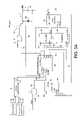
- FIG. 1Bshows a discontinuous switching voltage regulator according to an embodiment of the present invention comprising an inductor, switching circuitry, and switch control circuitry for controlling the switching circuitry in response to an error signal representing a difference between a propagation oscillation signal and a reference oscillation signal.
- FIG. 2Aillustrates an inductor current relative to an error signal as well as an on-time, discharge time, and tristate time of a cycle, according to one embodiment of the present invention.
- FIG. 2Bis a state diagram illustrating an embodiment of the present invention wherein the on-time is reduced if the ratio of the tristate time to the switch time exceeds a predetermined threshold.
- FIG. 3Ashows example circuitry for implementing a discontinuous switching voltage regulator according to an embodiment of the present invention, including a state mapper for implementing the state diagram of FIG. 2B and state controller circuitry.
- FIGS. 4A-4Dillustrate operation of a discontinuous switching voltage regulator according to an embodiment of the present invention, including the inductor current, the load current, the error signal, the data rate of the system circuitry, and the output voltage.
- FIG. 1Ashows an embodiment of the present invention comprising a discontinuous switching voltage regulator including a charging element 2 operable to generate an output voltage 4 , switching circuitry 6 coupled to the charging element 2 , and switch control circuitry 8 operable to control the switching circuitry 6 to configure the charging element 2 during a cycle, including to charge the charging element 2 for an on-time, discharge the charging element 2 for a discharge time, and tristate the charging element 2 for a tristate time.
- the on-timeis initialized to a first on-time, and a first switch time is measured comprising the first on-time and a first discharge time of a first cycle.
- a first tristate time of the first cycleis also measured, and a first ratio of the first tristate time to the first switch time is determined. The first ratio is compared to a first ratio threshold, and the on-time is adjusted to a second on-time if the first ratio exceeds the first ratio threshold.
- the switch control circuitry 8when the output voltage 4 falls below the reference voltage 12 , the resulting error signal 14 triggers the switch control circuitry 8 to begin a cycle by turning on a FET 6 A to charge the charging element 2 for the on-time, thereby building a charge across a capacitor 16 .
- the switch control circuitry 8turns off the FET 6 A so that the inductor current discharges while recirculating through a diode 6 B to ground.
- the diode 6 Bstops conducting, thereby preventing the output capacitor 16 from discharging through the inductor 2 to ground.
- the inductor 2remains in this tristate condition during the tristate time until the output voltage 4 falls below the reference voltage 12 (and the error signal turns positive), as shown in FIG. 2A .
- the diode 6 Bis replaced with a FET and a current sensor, wherein the FET is turned off when the current sensor detects zero current flowing through the FET at the end of the discharge time.
- the error signal 14may be generated in any suitable manner.
- FIG. 1Bshows an embodiment of the present invention wherein the error signal 14 is generated by a cycle comparator 18 which compares a propagation oscillation signal 20 to a reference oscillation signal 22 output by a frequency generator 24 .
- An oscillator 26generates the propagation oscillation signal 20 which represents a propagation delay of a digital circuit within the system circuitry 11 .
- the error signal 14may represent a phase or frequency error between the propagation oscillation signal 20 and the reference oscillation signal 22 output by the frequency generator 24 .
- FIG. 2Bis a state diagram illustrating how the on-time is adjusted according to an embodiment of the present invention.
- Operation of the discontinuous switching voltage regulatorbegins in STATE 1 where the on-time is initialized to a first on-time.
- the first on-timeis selected to maximize the peak inductor current while preventing damage to the FET 6 A (e.g., an on-time that corresponds to the maximum peak current the FET 6 A can handle minus a predetermined margin).
- a first switch time (T SW )is measured comprising the first on-time (T ON ) and a first discharge time (T REC ) of the inductor 2 .
- a first tristate time of the first cycleis also measured, and a first ratio (T TRI /T SW ) of the first tristate time to the first switch time is determined at branch 28 . If the first ratio is greater than a first ratio threshold (e.g., 3) at branch 28 , then at step 30 the on-time (T ON ) is adjusted to a second on-time by reducing the on-time by 25%, and the state changes to STATE 2 . Otherwise, the on-time (T ON ) is not adjusted and the state remains in STATE 1 . Any suitable value may be selected for the ratio threshold. For example, the first ratio threshold may be selected relative to the number of states in the state diagram, and/or relative to the range of on-times.
- a first ratio thresholde.g., 3
- a second switch time (T SW )is measured comprising the second on-time (T ON ) and a second discharge time (T REC ) of the inductor 2 .
- a second tristate time (T TRI ) of the second cycleis also measured, and a second ratio (T TRI /T SW ) of the second tristate time to the second switch time is determined at branch 32 . If the second ratio is greater than a second ratio threshold (e.g., 3) at branch 32 , then at step 34 the on-time (T ON ) is adjusted to a third on-time by reducing the on-time by 25%, and the state changes to STATE 3 .
- a second ratio thresholde.g., 3
- the second on-timeis approximately 1/N times the first on-time
- the third on-timeis approximately 1/N times the second on-time, and so on for the on-time of the following states. If the second ratio is not greater than the second ratio threshold at branch 32 , then the second ratio is compared to a third ratio threshold (e.g., 0.75) at branch 36 . If the second ratio is less than the third ratio threshold at branch 36 , then the on-time is reset to the first on-time, and the state changes to STATE 1 . Otherwise, the on-time (T ON ) is not adjusted, and the state remains in STATE 2 . Assuming the state changes to STATE 3 , a third switch time and a third tristate time are measured during a third cycle, a similar ratio generated and compared to a third ratio threshold at step 38 , and the on-time adjusted accordingly at step 40 .
- a third ratio thresholde.g. 0.5
- the state diagram of FIG. 2Bmay comprise any suitable number of states, and may also be modified in any suitable manner. Adjusting the on-time relative to the ratio of the tristate time to the switch time may improve the transient response without requiring an analog current sensor or a programmable analog current comparator as in the prior art.
- FIG. 3Ashows circuitry for implementing a discontinuous switching voltage regulator according to an embodiment of the present invention, wherein the error signal 14 is generated by comparing a propagation oscillation signal 20 to a reference oscillation signal 22 .
- the circuitry disclosed in FIG. 3Amay also be employed in an embodiment wherein the error signal 14 is generated using a different method, for example, by comparing the output voltage 4 to a reference voltage 12 as shown in FIG. 1A .
- the circuitry in FIG. 3Acomprises state mapper circuitry 42 for implementing the state diagram of FIG. 2B , and state controller circuitry 44 for generating three state signals S 0 , S 1 and S 2 corresponding to three states of the switching voltage regulator T TRI , T ON , and T REC .
- the state mapper circuitry 42may comprise any suitable circuitry for implementing the state diagram of FIG. 2B , such as a suitable state machine together with suitable math operators (multipliers, dividers, etc.) and/or code segments of a control program executed by a microprocessor.
- a power-on-reset (POR) signal 46is held high turning FET 6 A on through OR gate 48 until the output voltage 4 rises sufficiently for the oscillator 26 to function properly.
- POR 46is reset, the FET 6 A is turned off.
- the state controller 44is enabled via control signal 50 output by AND gate 51 .
- the state controller 44has been initialized to state S 0 (tristate time of FIG. 2A ).
- the state controller 44transitions from state S 0 to state S 1 (on-time of FIG. 2A ), which turns on FET 6 A via control signal 52 and enables via control signal 54 a digital timer (counter) 56 to begin timing the switch time (T SW ).
- the state controller 44also loads the on-time 58 generated by the state mapper 42 into a counter 60 (via control line 61 ) and enables the counter 60 via control line 63 .
- the counter 60generates a DONE signal 62 at the end of the on-time.
- the state controller 44transitions from state S 1 to state S 2 , loads a maximum discharge time into counter 60 , and begins monitoring the voltage 64 across the diode 6 B to detect the end of the discharge time.
- the maximum discharge timeis related to the inductor drive voltage (input voltage of the battery minus the output voltage Vdd in FIG. 1 ), and the flyback voltage that discharges the inductor 2 (Vdd plus the voltage across the diode 6 B). If the input voltage is much higher than the output voltage (plus the reverse bias voltage caused by the flyback diode), then the maximum off time is selected to be longer than the on-time.
- the state controller 44transitions from state S 2 to state S 0 and enables via control signal 66 a digital timer (counter) 68 for timing the next tristate time (T TRI ), and stops the counter 56 .
- the state controller 44loads via control signal 52 the switch time (T SW ) and the tristate time (T TRI ) into the state mapper 42 , which generates the next on-time according to the state diagram of FIG. 2B .
- the state mapper 42generates the next on-time in a manner that compensates for the delay in computing the next on-time.
- FIG. 3Bshows circuitry for implementing the state controller 44 of FIG. 3A according to an embodiment of the present invention.
- the 2-bit counter 70is initialized to state S 0 by the enable signal 50 (see FIG. 3A ).
- the 2-bit counter 70is enabled by a multiplexer 76 when the switching voltage regulator transitions into the next state. For example, when in state S 0 , the multiplexer 76 outputs control signal 78 as the enable signal 80 to the 2-bit counter 70 .
- control signal 78enables the 2-bit counter 70 which transitions from state S 0 to state S 1 .
- the multiplexer 76enables the 2-bit counter 70 which transitions from state S 1 to state S 2 .
- the voltage across the diode 6 Btransitions from a high to low logic level (over a certain interval) and then eventually rises from a low to high logic level at the end of the discharge time.
- a latch 82is used to detect the low to high transition of voltage 64 at the end of the discharge time.
- the latch 82When the voltage 64 transitions from high to low at the end of the on-time, the latch 82 enables an AND gate 84 which then detects the transition from low to high at the end of the discharge time. Alternatively, an AND gate 86 detects if the counter 60 ( FIG. 3A ) times out before the voltage 64 transitions from low to high. An OR gate 88 outputs the control signal 90 indicating the end of the discharge time, which enables the 2-bit counter 70 to transition from state S 2 back to state S 0 which activates control signal 66 to begin timing the tristate time.
- FIGS. 4A-4Billustrate operation of the switching voltage regulator, including the inductor current, load current, error signal, data rate, and output voltage.
- the error signalis high and the state mapper 42 remains in STATE 1 ( FIG. 2B ) until the output voltage rises to an operating level. Once the output voltage stabilizes, the state mapper 42 reduces the on-time and transitions into STATE 2 and then into STATE 3 .
- the state mapper 42further reduces the on-time and transitions into STATE 4 .
- the state mapper 42resets the on-time to the maximum and transitions into STATE 1 as shown in FIG.
Landscapes
- Engineering & Computer Science (AREA)
- Power Engineering (AREA)
- Dc-Dc Converters (AREA)
Abstract
Description
Claims (32)
Priority Applications (1)
| Application Number | Priority Date | Filing Date | Title |
|---|---|---|---|
| US11/590,704US7330019B1 (en) | 2006-10-31 | 2006-10-31 | Adjusting on-time for a discontinuous switching voltage regulator |
Applications Claiming Priority (1)
| Application Number | Priority Date | Filing Date | Title |
|---|---|---|---|
| US11/590,704US7330019B1 (en) | 2006-10-31 | 2006-10-31 | Adjusting on-time for a discontinuous switching voltage regulator |
Publications (1)
| Publication Number | Publication Date |
|---|---|
| US7330019B1true US7330019B1 (en) | 2008-02-12 |
Family
ID=39031465
Family Applications (1)
| Application Number | Title | Priority Date | Filing Date |
|---|---|---|---|
| US11/590,704ActiveUS7330019B1 (en) | 2006-10-31 | 2006-10-31 | Adjusting on-time for a discontinuous switching voltage regulator |
Country Status (1)
| Country | Link |
|---|---|
| US (1) | US7330019B1 (en) |
Cited By (120)
| Publication number | Priority date | Publication date | Assignee | Title |
|---|---|---|---|---|
| US20080224673A1 (en)* | 2007-03-14 | 2008-09-18 | Advanced Analog Technology, Inc. | Circuit for starting up a synchronous step-up DC/DC converter and the method thereof |
| US7486060B1 (en) | 2006-03-30 | 2009-02-03 | Western Digital Technologies, Inc. | Switching voltage regulator comprising a cycle comparator for dynamic voltage scaling |
| US7551383B1 (en) | 2006-06-28 | 2009-06-23 | Western Digital Technologies, Inc. | Adjusting voltage delivered to disk drive circuitry based on a selected zone |
| US20100014328A1 (en)* | 2008-07-18 | 2010-01-21 | Qisda Corporation | Direct Current Generator and the Pulse generator thereof |
| US20100052629A1 (en)* | 2007-04-04 | 2010-03-04 | Kwan-Jen Chu | Adaptive zero current sense apparatus and method for a switching regulator |
| US7733189B1 (en) | 2007-09-14 | 2010-06-08 | Western Digital Technologies, Inc. | Oscillator comprising foldover detection |
| US8085020B1 (en) | 2008-06-13 | 2011-12-27 | Western Digital Technologies, Inc. | Switching voltage regulator employing dynamic voltage scaling with hysteretic comparator |
| US8324974B1 (en) | 2010-12-17 | 2012-12-04 | Western Digital Technologies, Inc. | Regulating power consumption of digital circuitry using a multi-layer ring oscillator |
| US8350628B1 (en) | 2011-02-15 | 2013-01-08 | Western Digital Technologies, Inc. | Gate speed regulator dithering ring oscillator to match critical path circuit |
| US8390367B1 (en) | 2011-02-15 | 2013-03-05 | Western Digital Technologies, Inc. | Ensuring minimum gate speed during startup of gate speed regulator |
| US8427130B2 (en) | 2010-12-16 | 2013-04-23 | Integrated Device Technology, Inc. | Methods and apparatuses for combined frequency compensation and soft start processes |
| US8513935B2 (en) | 2010-12-16 | 2013-08-20 | Integrated Device Technology, Inc. | Combinations of current feedback for frequency compensation, overload detection, and super overload detection in switching power converters |
| US8598856B1 (en)* | 2010-02-25 | 2013-12-03 | International Rectifier Corporation | Power supply switching and discontinuous power supply mode |
| US8824081B1 (en) | 2012-03-13 | 2014-09-02 | Western Digital Technologies, Inc. | Disk drive employing radially coherent reference pattern for servo burst demodulation and fly height measurement |
| US8830617B1 (en) | 2013-05-30 | 2014-09-09 | Western Digital Technologies, Inc. | Disk drive adjusting state estimator to compensate for unreliable servo data |
| TWI456381B (en)* | 2010-02-25 | 2014-10-11 | Int Rectifier Corp | Method and system of power supply |
| US8879191B1 (en) | 2012-11-14 | 2014-11-04 | Western Digital Technologies, Inc. | Disk drive modifying rotational position optimization algorithm to achieve target performance for limited stroke |
| US8891191B1 (en) | 2014-05-06 | 2014-11-18 | Western Digital Technologies, Inc. | Data storage device initializing read signal gain to detect servo seed pattern |
| US8891194B1 (en) | 2013-05-14 | 2014-11-18 | Western Digital Technologies, Inc. | Disk drive iteratively adapting correction value that compensates for non-linearity of head |
| US8896957B1 (en) | 2013-05-10 | 2014-11-25 | Western Digital Technologies, Inc. | Disk drive performing spiral scan of disk surface to detect residual data |
| US8902539B1 (en) | 2014-05-13 | 2014-12-02 | Western Digital Technologies, Inc. | Data storage device reducing seek power consumption |
| US8902538B1 (en) | 2013-03-29 | 2014-12-02 | Western Digital Technologies, Inc. | Disk drive detecting crack in microactuator |
| US8913342B1 (en) | 2014-03-21 | 2014-12-16 | Western Digital Technologies, Inc. | Data storage device adjusting range of microactuator digital-to-analog converter based on operating temperature |
| US8917474B1 (en) | 2011-08-08 | 2014-12-23 | Western Digital Technologies, Inc. | Disk drive calibrating a velocity profile prior to writing a spiral track |
| US8917475B1 (en) | 2013-12-20 | 2014-12-23 | Western Digital Technologies, Inc. | Disk drive generating a disk locked clock using radial dependent timing feed-forward compensation |
| US8922938B1 (en) | 2012-11-02 | 2014-12-30 | Western Digital Technologies, Inc. | Disk drive filtering disturbance signal and error signal for adaptive feed-forward compensation |
| US8922931B1 (en) | 2013-05-13 | 2014-12-30 | Western Digital Technologies, Inc. | Disk drive releasing variable amount of buffered write data based on sliding window of predicted servo quality |
| US8922940B1 (en) | 2014-05-27 | 2014-12-30 | Western Digital Technologies, Inc. | Data storage device reducing spindle motor voltage boost during power failure |
| US8922937B1 (en) | 2012-04-19 | 2014-12-30 | Western Digital Technologies, Inc. | Disk drive evaluating multiple vibration sensor outputs to enable write-protection |
| US8929022B1 (en) | 2012-12-19 | 2015-01-06 | Western Digital Technologies, Inc. | Disk drive detecting microactuator degradation by evaluating frequency component of servo signal |
| US8929021B1 (en) | 2012-03-27 | 2015-01-06 | Western Digital Technologies, Inc. | Disk drive servo writing from spiral tracks using radial dependent timing feed-forward compensation |
| US8934186B1 (en) | 2014-03-26 | 2015-01-13 | Western Digital Technologies, Inc. | Data storage device estimating servo zone to reduce size of track address |
| US8937404B1 (en) | 2010-08-23 | 2015-01-20 | Western Digital Technologies, Inc. | Data storage device comprising dual mode independent/parallel voltage regulators |
| US8937784B1 (en) | 2012-08-01 | 2015-01-20 | Western Digital Technologies, Inc. | Disk drive employing feed-forward compensation and phase shift compensation during seek settling |
| US8941945B1 (en) | 2014-06-06 | 2015-01-27 | Western Digital Technologies, Inc. | Data storage device servoing heads based on virtual servo tracks |
| US8941939B1 (en) | 2013-10-24 | 2015-01-27 | Western Digital Technologies, Inc. | Disk drive using VCM BEMF feed-forward compensation to write servo data to a disk |
| US8947819B1 (en) | 2012-08-28 | 2015-02-03 | Western Digital Technologies, Inc. | Disk drive implementing hysteresis for primary shock detector based on a more sensitive secondary shock detector |
| US8953271B1 (en) | 2013-05-13 | 2015-02-10 | Western Digital Technologies, Inc. | Disk drive compensating for repeatable run out selectively per zone |
| US8953278B1 (en) | 2011-11-16 | 2015-02-10 | Western Digital Technologies, Inc. | Disk drive selecting disturbance signal for feed-forward compensation |
| US8958169B1 (en) | 2014-06-11 | 2015-02-17 | Western Digital Technologies, Inc. | Data storage device re-qualifying state estimator while decelerating head |
| US8970979B1 (en) | 2013-12-18 | 2015-03-03 | Western Digital Technologies, Inc. | Disk drive determining frequency response of actuator near servo sample frequency |
| US8970191B1 (en)* | 2010-02-01 | 2015-03-03 | National Semiconductor Corporation | On/off time modulation for constant on-time and constant off-time switching regulators |
| US8982501B1 (en) | 2014-09-22 | 2015-03-17 | Western Digital Technologies, Inc. | Data storage device compensating for repeatable disturbance when commutating a spindle motor |
| US8982490B1 (en) | 2014-04-24 | 2015-03-17 | Western Digital Technologies, Inc. | Data storage device reading first spiral track while simultaneously writing second spiral track |
| US8995082B1 (en) | 2011-06-03 | 2015-03-31 | Western Digital Technologies, Inc. | Reducing acoustic noise in a disk drive when exiting idle mode |
| US8995075B1 (en) | 2012-06-21 | 2015-03-31 | Western Digital Technologies, Inc. | Disk drive adjusting estimated servo state to compensate for transient when crossing a servo zone boundary |
| US9001454B1 (en) | 2013-04-12 | 2015-04-07 | Western Digital Technologies, Inc. | Disk drive adjusting phase of adaptive feed-forward controller when reconfiguring servo loop |
| US9007714B1 (en) | 2014-07-18 | 2015-04-14 | Western Digital Technologies Inc. | Data storage device comprising slew rate anti-windup compensation for microactuator |
| US9013825B1 (en) | 2014-03-24 | 2015-04-21 | Western Digital Technologies, Inc. | Electronic system with vibration management mechanism and method of operation thereof |
| US9013824B1 (en) | 2014-06-04 | 2015-04-21 | Western Digital Technologies, Inc. | Data storage device comprising dual read sensors and dual servo channels to improve servo demodulation |
| US9025269B1 (en) | 2014-01-02 | 2015-05-05 | Western Digital Technologies, Inc. | Disk drive compensating for cycle slip of disk locked clock when reading mini-wedge |
| US9026728B1 (en) | 2013-06-06 | 2015-05-05 | Western Digital Technologies, Inc. | Disk drive applying feed-forward compensation when writing consecutive data tracks |
| US9047932B1 (en) | 2014-03-21 | 2015-06-02 | Western Digital Technologies, Inc. | Data storage device adjusting a power loss threshold based on samples of supply voltage |
| US9047901B1 (en) | 2013-05-28 | 2015-06-02 | Western Digital Technologies, Inc. | Disk drive measuring spiral track error by measuring a slope of a spiral track across a disk radius |
| US9047919B1 (en) | 2013-03-12 | 2015-06-02 | Western Digitial Technologies, Inc. | Disk drive initializing servo read channel by reading data preceding servo preamble during access operation |
| US9053726B1 (en) | 2014-01-29 | 2015-06-09 | Western Digital Technologies, Inc. | Data storage device on-line adapting disturbance observer filter |
| US9053727B1 (en) | 2014-06-02 | 2015-06-09 | Western Digital Technologies, Inc. | Disk drive opening spiral crossing window based on DC and AC spiral track error |
| US9053712B1 (en) | 2014-05-07 | 2015-06-09 | Western Digital Technologies, Inc. | Data storage device reading servo sector while writing data sector |
| US9058834B1 (en) | 2013-11-08 | 2015-06-16 | Western Digital Technologies, Inc. | Power architecture for low power modes in storage devices |
| US9058826B1 (en) | 2014-02-13 | 2015-06-16 | Western Digital Technologies, Inc. | Data storage device detecting free fall condition from disk speed variations |
| US9058827B1 (en) | 2013-06-25 | 2015-06-16 | Western Digitial Technologies, Inc. | Disk drive optimizing filters based on sensor signal and disturbance signal for adaptive feed-forward compensation |
| US9064537B1 (en) | 2013-09-13 | 2015-06-23 | Western Digital Technologies, Inc. | Disk drive measuring radial offset between heads by detecting a difference between ramp contact |
| US9076472B1 (en) | 2014-08-21 | 2015-07-07 | Western Digital (Fremont), Llc | Apparatus enabling writing servo data when disk reaches target rotation speed |
| US9076471B1 (en) | 2013-07-31 | 2015-07-07 | Western Digital Technologies, Inc. | Fall detection scheme using FFS |
| US9076490B1 (en) | 2012-12-12 | 2015-07-07 | Western Digital Technologies, Inc. | Disk drive writing radial offset spiral servo tracks by reading spiral seed tracks |
| US9076473B1 (en) | 2014-08-12 | 2015-07-07 | Western Digital Technologies, Inc. | Data storage device detecting fly height instability of head during load operation based on microactuator response |
| US9093105B2 (en) | 2011-12-09 | 2015-07-28 | Western Digital Technologies, Inc. | Disk drive charging capacitor using motor supply voltage during power failure |
| US9099147B1 (en) | 2014-09-22 | 2015-08-04 | Western Digital Technologies, Inc. | Data storage device commutating a spindle motor using closed-loop rotation phase alignment |
| US9111575B1 (en) | 2014-10-23 | 2015-08-18 | Western Digital Technologies, Inc. | Data storage device employing adaptive feed-forward control in timing loop to compensate for vibration |
| US9129630B1 (en) | 2014-12-16 | 2015-09-08 | Western Digital Technologies, Inc. | Data storage device employing full servo sectors on first disk surface and mini servo sectors on second disk surface |
| US9142235B1 (en) | 2009-10-27 | 2015-09-22 | Western Digital Technologies, Inc. | Disk drive characterizing microactuator by injecting sinusoidal disturbance and evaluating feed-forward compensation values |
| US9142225B1 (en) | 2014-03-21 | 2015-09-22 | Western Digital Technologies, Inc. | Electronic system with actuator control mechanism and method of operation thereof |
| US9142249B1 (en) | 2013-12-06 | 2015-09-22 | Western Digital Technologies, Inc. | Disk drive using timing loop control signal for vibration compensation in servo loop |
| US9141177B1 (en) | 2014-03-21 | 2015-09-22 | Western Digital Technologies, Inc. | Data storage device employing glitch compensation for power loss detection |
| US9147418B1 (en) | 2013-06-20 | 2015-09-29 | Western Digital Technologies, Inc. | Disk drive compensating for microactuator gain variations |
| US9147428B1 (en) | 2013-04-24 | 2015-09-29 | Western Digital Technologies, Inc. | Disk drive with improved spin-up control |
| US9155139B2 (en) | 2012-03-09 | 2015-10-06 | Rockwell Automation Technologies, Inc. | LED driver circuits and methods |
| US9153283B1 (en) | 2014-09-30 | 2015-10-06 | Western Digital Technologies, Inc. | Data storage device compensating for hysteretic response of microactuator |
| US9165583B1 (en) | 2014-10-29 | 2015-10-20 | Western Digital Technologies, Inc. | Data storage device adjusting seek profile based on seek length when ending track is near ramp |
| US9171567B1 (en) | 2014-05-27 | 2015-10-27 | Western Digital Technologies, Inc. | Data storage device employing sliding mode control of spindle motor |
| US9171568B1 (en) | 2014-06-25 | 2015-10-27 | Western Digital Technologies, Inc. | Data storage device periodically re-initializing spindle motor commutation sequence based on timing data |
| US9208810B1 (en) | 2014-04-24 | 2015-12-08 | Western Digital Technologies, Inc. | Data storage device attenuating interference from first spiral track when reading second spiral track |
| US9208808B1 (en) | 2014-04-22 | 2015-12-08 | Western Digital Technologies, Inc. | Electronic system with unload management mechanism and method of operation thereof |
| US9208815B1 (en) | 2014-10-09 | 2015-12-08 | Western Digital Technologies, Inc. | Data storage device dynamically reducing coast velocity during seek to reduce power consumption |
| US9214175B1 (en) | 2015-03-16 | 2015-12-15 | Western Digital Technologies, Inc. | Data storage device configuring a gain of a servo control system for actuating a head over a disk |
| US9230592B1 (en) | 2014-12-23 | 2016-01-05 | Western Digital Technologies, Inc. | Electronic system with a method of motor spindle bandwidth estimation and calibration thereof |
| US9230593B1 (en) | 2014-12-23 | 2016-01-05 | Western Digital Technologies, Inc. | Data storage device optimizing spindle motor power when transitioning into a power failure mode |
| US9245560B1 (en) | 2015-03-09 | 2016-01-26 | Western Digital Technologies, Inc. | Data storage device measuring reader/writer offset by reading spiral track and concentric servo sectors |
| US9245540B1 (en) | 2014-10-29 | 2016-01-26 | Western Digital Technologies, Inc. | Voice coil motor temperature sensing circuit to reduce catastrophic failure due to voice coil motor coil shorting to ground |
| US9245577B1 (en) | 2015-03-26 | 2016-01-26 | Western Digital Technologies, Inc. | Data storage device comprising spindle motor current sensing with supply voltage noise attenuation |
| US9251823B1 (en) | 2014-12-10 | 2016-02-02 | Western Digital Technologies, Inc. | Data storage device delaying seek operation to avoid thermal asperities |
| US9269386B1 (en) | 2014-01-29 | 2016-02-23 | Western Digital Technologies, Inc. | Data storage device on-line adapting disturbance observer filter |
| US9286925B1 (en) | 2015-03-26 | 2016-03-15 | Western Digital Technologies, Inc. | Data storage device writing multiple burst correction values at the same radial location |
| US9286927B1 (en) | 2014-12-16 | 2016-03-15 | Western Digital Technologies, Inc. | Data storage device demodulating servo burst by computing slope of intermediate integration points |
| US9343094B1 (en) | 2015-03-26 | 2016-05-17 | Western Digital Technologies, Inc. | Data storage device filtering burst correction values before downsampling the burst correction values |
| US9343102B1 (en) | 2015-03-25 | 2016-05-17 | Western Digital Technologies, Inc. | Data storage device employing a phase offset to generate power from a spindle motor during a power failure |
| US9349401B1 (en) | 2014-07-24 | 2016-05-24 | Western Digital Technologies, Inc. | Electronic system with media scan mechanism and method of operation thereof |
| US9350278B1 (en) | 2014-06-13 | 2016-05-24 | Western Digital Technologies, Inc. | Circuit technique to integrate voice coil motor support elements |
| US9355676B1 (en) | 2015-03-25 | 2016-05-31 | Western Digital Technologies, Inc. | Data storage device controlling amplitude and phase of driving voltage to generate power from a spindle motor |
| US9355667B1 (en) | 2014-11-11 | 2016-05-31 | Western Digital Technologies, Inc. | Data storage device saving absolute position at each servo wedge for previous write operations |
| US9361939B1 (en) | 2014-03-10 | 2016-06-07 | Western Digital Technologies, Inc. | Data storage device characterizing geometry of magnetic transitions |
| US9396751B1 (en) | 2015-06-26 | 2016-07-19 | Western Digital Technologies, Inc. | Data storage device compensating for fabrication tolerances when measuring spindle motor current |
| US9407015B1 (en) | 2014-12-29 | 2016-08-02 | Western Digital Technologies, Inc. | Automatic power disconnect device |
| US9418689B2 (en) | 2014-10-09 | 2016-08-16 | Western Digital Technologies, Inc. | Data storage device generating an operating seek time profile as a function of a base seek time profile |
| US9424871B1 (en) | 2012-09-13 | 2016-08-23 | Western Digital Technologies, Inc. | Disk drive correcting an error in a detected gray code |
| US9424868B1 (en) | 2015-05-12 | 2016-08-23 | Western Digital Technologies, Inc. | Data storage device employing spindle motor driving profile during seek to improve power performance |
| US9437237B1 (en) | 2015-02-20 | 2016-09-06 | Western Digital Technologies, Inc. | Method to detect power loss through data storage device spindle speed |
| US9437231B1 (en) | 2015-09-25 | 2016-09-06 | Western Digital Technologies, Inc. | Data storage device concurrently controlling and sensing a secondary actuator for actuating a head over a disk |
| US9454212B1 (en) | 2014-12-08 | 2016-09-27 | Western Digital Technologies, Inc. | Wakeup detector |
| US9471072B1 (en) | 2013-11-14 | 2016-10-18 | Western Digital Technologies, Inc | Self-adaptive voltage scaling |
| US9484733B1 (en) | 2013-09-11 | 2016-11-01 | Western Digital Technologies, Inc. | Power control module for data storage device |
| US9542966B1 (en) | 2015-07-09 | 2017-01-10 | Western Digital Technologies, Inc. | Data storage devices and methods with frequency-shaped sliding mode control |
| US9564162B1 (en) | 2015-12-28 | 2017-02-07 | Western Digital Technologies, Inc. | Data storage device measuring resonant frequency of a shock sensor by applying differential excitation and measuring oscillation |
| US9581978B1 (en) | 2014-12-17 | 2017-02-28 | Western Digital Technologies, Inc. | Electronic system with servo management mechanism and method of operation thereof |
| US9620160B1 (en) | 2015-12-28 | 2017-04-11 | Western Digital Technologies, Inc. | Data storage device measuring resonant frequency of a shock sensor by inserting the shock sensor into an oscillator circuit |
| US9823294B1 (en) | 2013-10-29 | 2017-11-21 | Western Digital Technologies, Inc. | Negative voltage testing methodology and tester |
| US9886285B2 (en) | 2015-03-31 | 2018-02-06 | Western Digital Technologies, Inc. | Communication interface initialization |
| US9899834B1 (en) | 2015-11-18 | 2018-02-20 | Western Digital Technologies, Inc. | Power control module using protection circuit for regulating backup voltage to power load during power fault |
| US9959204B1 (en) | 2015-03-09 | 2018-05-01 | Western Digital Technologies, Inc. | Tracking sequential ranges of non-ordered data |
| US20190140542A1 (en)* | 2017-10-30 | 2019-05-09 | Renesas Electronics America Inc. | Asynchronous controller for low power hysteretic buck-boost dc-dc controller |
Citations (51)
| Publication number | Priority date | Publication date | Assignee | Title |
|---|---|---|---|---|
| US4675617A (en) | 1986-02-03 | 1987-06-23 | Martin Kenneth W | Stable voltage controlled oscillator |
| US4737670A (en) | 1984-11-09 | 1988-04-12 | Lsi Logic Corporation | Delay control circuit |
| US4822144A (en) | 1986-12-24 | 1989-04-18 | U.S. Philips Corporation | Electro-optic color display including luminescent layer and interference filter |
| US4922141A (en) | 1986-10-07 | 1990-05-01 | Western Digital Corporation | Phase-locked loop delay line |
| US5146121A (en) | 1991-10-24 | 1992-09-08 | Northern Telecom Limited | Signal delay apparatus employing a phase locked loop |
| US5440250A (en) | 1993-06-26 | 1995-08-08 | Deutsche Itt Industries Gmbh | Clock-generating circuit for clock-controlled logic circuits |
| US5440520A (en) | 1994-09-16 | 1995-08-08 | Intel Corporation | Integrated circuit device that selects its own supply voltage by controlling a power supply |
| US5479119A (en) | 1994-11-23 | 1995-12-26 | Analog Devices, Inc. | High speed active overvoltage detection and protection for overvoltage sensitive circuits |
| US5612610A (en) | 1993-10-22 | 1997-03-18 | Sgs-Thomson Microelectronics S.R.L | DC-to-DC converter operating in a discontinuous mode |
| US5629610A (en)* | 1994-05-06 | 1997-05-13 | Sgs-Thomson Microelectronics S.R.L. | Dual threshold current mode digital PWM controller |
| US5638019A (en) | 1995-11-17 | 1997-06-10 | International Business Machines Corporation | Accurately generating precisely skewed clock signals |
| US5661422A (en) | 1995-12-12 | 1997-08-26 | Analog Devices, Inc. | High speed saturation prevention for saturable circuit elements |
| US5747976A (en)* | 1996-03-26 | 1998-05-05 | Raytheon Company | Constant on-time architecture for switching regulators |
| US5748050A (en) | 1996-03-29 | 1998-05-05 | Symbios Logic Inc. | Linearization method and apparatus for voltage controlled oscillator |
| US5777567A (en) | 1996-06-14 | 1998-07-07 | Sun Microsystems, Inc. | System and method for serial to parallel data conversion using delay line |
| US5787292A (en) | 1996-04-01 | 1998-07-28 | International Business Machines Corporation | Power saving method and apparatus for use in multiple frequency zone drives |
| US5808455A (en)* | 1996-11-13 | 1998-09-15 | Micro Linear Corporation | DC-to-DC converter having hysteretic current limiting |
| US5994885A (en) | 1993-03-23 | 1999-11-30 | Linear Technology Corporation | Control circuit and method for maintaining high efficiency over broad current ranges in a switching regulator circuit |
| US6055287A (en) | 1998-05-26 | 2000-04-25 | Mcewan; Thomas E. | Phase-comparator-less delay locked loop |
| US6125157A (en) | 1997-02-06 | 2000-09-26 | Rambus, Inc. | Delay-locked loop circuitry for clock delay adjustment |
| US6157247A (en) | 1996-08-07 | 2000-12-05 | Motorola, Inc. | Methods and circuits for dynamically adjusting a supply voltage and/or a frequency of a clock signal in a digital circuit |
| US6259293B1 (en) | 1999-06-15 | 2001-07-10 | Mitsubishi Denki Kabushiki Kaisha | Delay circuitry, clock generating circuitry, and phase synchronization circuitry |
| US6333652B1 (en) | 1999-05-27 | 2001-12-25 | Rohm Co. Ltd. | Delay circuit |
| US6356062B1 (en) | 2000-09-27 | 2002-03-12 | Intel Corporation | Degenerative load temperature correction for charge pumps |
| US6424184B1 (en) | 1996-09-25 | 2002-07-23 | Matsushita Electric Industrial Co., Ltd. | Frequency-voltage conversion circuit, delay amount judgement circuit, system having frequency-voltage conversion circuit, method of adjusting input/output characteristics of frequency-voltage conversion circuit, and apparatus for automatically adjusting input |
| US6425086B1 (en) | 1999-04-30 | 2002-07-23 | Intel Corporation | Method and apparatus for dynamic power control of a low power processor |
| US6449575B2 (en) | 1999-04-21 | 2002-09-10 | Hewlett-Packard Company | Voltage control of integrated circuits |
| US6515460B1 (en) | 2001-09-10 | 2003-02-04 | National Semiconductor Corporation | Multiphase switching regulator control architecture for low on time systems that enforces current sharing |
| US6525585B1 (en) | 2000-11-21 | 2003-02-25 | Nec Corporation | Fixed-length delay generation circuit |
| US6535735B2 (en) | 2001-03-22 | 2003-03-18 | Skyworks Solutions, Inc. | Critical path adaptive power control |
| US20030093160A1 (en) | 2001-11-09 | 2003-05-15 | The Regents Of The University Of Colorado, A Body Corporate | Adaptive voltage regulator for powered digital devices |
| US6577535B2 (en) | 2001-02-16 | 2003-06-10 | Sandisk Corporation | Method and system for distributed power generation in multi-chip memory systems |
| US6617936B2 (en) | 2001-02-20 | 2003-09-09 | Velio Communications, Inc. | Phase controlled oscillator |
| US6622252B1 (en) | 2000-04-12 | 2003-09-16 | International Business Machines Corporation | Data storage device having selectable performance modes for use in dual powered portable devices |
| US6657467B2 (en) | 2001-08-10 | 2003-12-02 | Sony Corporation | Delay control circuit with internal power supply voltage control |
| US6693473B2 (en) | 2002-03-19 | 2004-02-17 | Infineon Technologies Ag | Delay lock loop having a variable voltage regulator |
| US6831494B1 (en) | 2003-05-16 | 2004-12-14 | Transmeta Corporation | Voltage compensated integrated circuits |
| US20040257056A1 (en) | 2003-05-09 | 2004-12-23 | Jian-Rong Huang | Switching regulator with improved load transient efficiency and method thereof |
| US6868503B1 (en) | 2002-01-19 | 2005-03-15 | National Semiconductor Corporation | Adaptive voltage scaling digital processing component and method of operating the same |
| US6870410B1 (en) | 2002-10-15 | 2005-03-22 | National Semiconductor Corporation | All digital power supply system and method that provides a substantially constant supply voltage over changes in PVT without a band gap reference voltage |
| US6885210B1 (en) | 2002-04-16 | 2005-04-26 | Transmeta Corporation | System and method for measuring transistor leakage current with a ring oscillator with backbias controls |
| US6909266B2 (en) | 2002-11-14 | 2005-06-21 | Fyre Storm, Inc. | Method of regulating an output voltage of a power converter by calculating a current value to be applied to an inductor during a time interval immediately following a voltage sensing time interval and varying a duty cycle of a switch during the time interval following the voltage sensing time interval |
| US20050134391A1 (en) | 2003-12-19 | 2005-06-23 | Yasuyuki Kimura | Semiconductor integrated circuit having built-in PLL circuit |
| US20050140418A1 (en) | 2003-12-31 | 2005-06-30 | Ravisangar Muniandy | On-chip frequency degradation compensation |
| US20050218877A1 (en) | 2004-03-31 | 2005-10-06 | Matsushita Electric Industrial Co., Ltd. | Current mode switching regulator with predetermined on time |
| US20050218871A1 (en) | 2003-04-11 | 2005-10-06 | Inyup Kang | Dynamic voltage scaling for portable devices |
| US6987380B1 (en) | 2001-11-06 | 2006-01-17 | Linear Technology Corporation | Time-based current control in switching regulators |
| US7042202B2 (en) | 2002-07-10 | 2006-05-09 | Marvell World Trade Ltd | Energy saving discontinuous mode system and method |
| US7109695B2 (en) | 2004-12-08 | 2006-09-19 | Kiawe Forest Llc. | Adaptive digital voltage regulator with same-cycle feedback |
| US7129763B1 (en) | 2004-11-08 | 2006-10-31 | Western Digital Technologies, Inc. | Adjusting power consumption of digital circuitry by generating frequency error representing error in propagation delay |
| US7205805B1 (en) | 2004-11-02 | 2007-04-17 | Western Digital Technologies, Inc. | Adjusting power consumption of digital circuitry relative to critical path circuit having the largest propagation delay error |
- 2006
- 2006-10-31USUS11/590,704patent/US7330019B1/enactiveActive
Patent Citations (54)
| Publication number | Priority date | Publication date | Assignee | Title |
|---|---|---|---|---|
| US4737670A (en) | 1984-11-09 | 1988-04-12 | Lsi Logic Corporation | Delay control circuit |
| US4675617A (en) | 1986-02-03 | 1987-06-23 | Martin Kenneth W | Stable voltage controlled oscillator |
| US4922141A (en) | 1986-10-07 | 1990-05-01 | Western Digital Corporation | Phase-locked loop delay line |
| US4822144A (en) | 1986-12-24 | 1989-04-18 | U.S. Philips Corporation | Electro-optic color display including luminescent layer and interference filter |
| US5146121A (en) | 1991-10-24 | 1992-09-08 | Northern Telecom Limited | Signal delay apparatus employing a phase locked loop |
| US5994885A (en) | 1993-03-23 | 1999-11-30 | Linear Technology Corporation | Control circuit and method for maintaining high efficiency over broad current ranges in a switching regulator circuit |
| US5440250A (en) | 1993-06-26 | 1995-08-08 | Deutsche Itt Industries Gmbh | Clock-generating circuit for clock-controlled logic circuits |
| US5612610A (en) | 1993-10-22 | 1997-03-18 | Sgs-Thomson Microelectronics S.R.L | DC-to-DC converter operating in a discontinuous mode |
| US5629610A (en)* | 1994-05-06 | 1997-05-13 | Sgs-Thomson Microelectronics S.R.L. | Dual threshold current mode digital PWM controller |
| US5440520A (en) | 1994-09-16 | 1995-08-08 | Intel Corporation | Integrated circuit device that selects its own supply voltage by controlling a power supply |
| US5479119A (en) | 1994-11-23 | 1995-12-26 | Analog Devices, Inc. | High speed active overvoltage detection and protection for overvoltage sensitive circuits |
| US5638019A (en) | 1995-11-17 | 1997-06-10 | International Business Machines Corporation | Accurately generating precisely skewed clock signals |
| US5661422A (en) | 1995-12-12 | 1997-08-26 | Analog Devices, Inc. | High speed saturation prevention for saturable circuit elements |
| US5747976A (en)* | 1996-03-26 | 1998-05-05 | Raytheon Company | Constant on-time architecture for switching regulators |
| US5748050A (en) | 1996-03-29 | 1998-05-05 | Symbios Logic Inc. | Linearization method and apparatus for voltage controlled oscillator |
| US6285263B1 (en) | 1996-03-29 | 2001-09-04 | Lsi Logic Corporation | Linearization method and apparatus for voltage controlled oscillator |
| US5787292A (en) | 1996-04-01 | 1998-07-28 | International Business Machines Corporation | Power saving method and apparatus for use in multiple frequency zone drives |
| US5777567A (en) | 1996-06-14 | 1998-07-07 | Sun Microsystems, Inc. | System and method for serial to parallel data conversion using delay line |
| US6157247A (en) | 1996-08-07 | 2000-12-05 | Motorola, Inc. | Methods and circuits for dynamically adjusting a supply voltage and/or a frequency of a clock signal in a digital circuit |
| US6424184B1 (en) | 1996-09-25 | 2002-07-23 | Matsushita Electric Industrial Co., Ltd. | Frequency-voltage conversion circuit, delay amount judgement circuit, system having frequency-voltage conversion circuit, method of adjusting input/output characteristics of frequency-voltage conversion circuit, and apparatus for automatically adjusting input |
| US5808455A (en)* | 1996-11-13 | 1998-09-15 | Micro Linear Corporation | DC-to-DC converter having hysteretic current limiting |
| US6125157A (en) | 1997-02-06 | 2000-09-26 | Rambus, Inc. | Delay-locked loop circuitry for clock delay adjustment |
| US6055287A (en) | 1998-05-26 | 2000-04-25 | Mcewan; Thomas E. | Phase-comparator-less delay locked loop |
| US6449575B2 (en) | 1999-04-21 | 2002-09-10 | Hewlett-Packard Company | Voltage control of integrated circuits |
| US6425086B1 (en) | 1999-04-30 | 2002-07-23 | Intel Corporation | Method and apparatus for dynamic power control of a low power processor |
| US6333652B1 (en) | 1999-05-27 | 2001-12-25 | Rohm Co. Ltd. | Delay circuit |
| US6259293B1 (en) | 1999-06-15 | 2001-07-10 | Mitsubishi Denki Kabushiki Kaisha | Delay circuitry, clock generating circuitry, and phase synchronization circuitry |
| US6622252B1 (en) | 2000-04-12 | 2003-09-16 | International Business Machines Corporation | Data storage device having selectable performance modes for use in dual powered portable devices |
| US6356062B1 (en) | 2000-09-27 | 2002-03-12 | Intel Corporation | Degenerative load temperature correction for charge pumps |
| US6525585B1 (en) | 2000-11-21 | 2003-02-25 | Nec Corporation | Fixed-length delay generation circuit |
| US6577535B2 (en) | 2001-02-16 | 2003-06-10 | Sandisk Corporation | Method and system for distributed power generation in multi-chip memory systems |
| US6617936B2 (en) | 2001-02-20 | 2003-09-09 | Velio Communications, Inc. | Phase controlled oscillator |
| US6535735B2 (en) | 2001-03-22 | 2003-03-18 | Skyworks Solutions, Inc. | Critical path adaptive power control |
| US6657467B2 (en) | 2001-08-10 | 2003-12-02 | Sony Corporation | Delay control circuit with internal power supply voltage control |
| US6515460B1 (en) | 2001-09-10 | 2003-02-04 | National Semiconductor Corporation | Multiphase switching regulator control architecture for low on time systems that enforces current sharing |
| US6987380B1 (en) | 2001-11-06 | 2006-01-17 | Linear Technology Corporation | Time-based current control in switching regulators |
| US20030093160A1 (en) | 2001-11-09 | 2003-05-15 | The Regents Of The University Of Colorado, A Body Corporate | Adaptive voltage regulator for powered digital devices |
| US7061292B2 (en) | 2001-11-09 | 2006-06-13 | The Regents Of The University Of Colorado | Adaptive voltage regulator for powered digital devices |
| US6868503B1 (en) | 2002-01-19 | 2005-03-15 | National Semiconductor Corporation | Adaptive voltage scaling digital processing component and method of operating the same |
| US6693473B2 (en) | 2002-03-19 | 2004-02-17 | Infineon Technologies Ag | Delay lock loop having a variable voltage regulator |
| US6885210B1 (en) | 2002-04-16 | 2005-04-26 | Transmeta Corporation | System and method for measuring transistor leakage current with a ring oscillator with backbias controls |
| US7042202B2 (en) | 2002-07-10 | 2006-05-09 | Marvell World Trade Ltd | Energy saving discontinuous mode system and method |
| US6870410B1 (en) | 2002-10-15 | 2005-03-22 | National Semiconductor Corporation | All digital power supply system and method that provides a substantially constant supply voltage over changes in PVT without a band gap reference voltage |
| US6909266B2 (en) | 2002-11-14 | 2005-06-21 | Fyre Storm, Inc. | Method of regulating an output voltage of a power converter by calculating a current value to be applied to an inductor during a time interval immediately following a voltage sensing time interval and varying a duty cycle of a switch during the time interval following the voltage sensing time interval |
| US20050218871A1 (en) | 2003-04-11 | 2005-10-06 | Inyup Kang | Dynamic voltage scaling for portable devices |
| US20040257056A1 (en) | 2003-05-09 | 2004-12-23 | Jian-Rong Huang | Switching regulator with improved load transient efficiency and method thereof |
| US6831494B1 (en) | 2003-05-16 | 2004-12-14 | Transmeta Corporation | Voltage compensated integrated circuits |
| US7015735B2 (en) | 2003-12-19 | 2006-03-21 | Renesas Technology Corp. | Semiconductor integrated circuit having built-in PLL circuit |
| US20050134391A1 (en) | 2003-12-19 | 2005-06-23 | Yasuyuki Kimura | Semiconductor integrated circuit having built-in PLL circuit |
| US20050140418A1 (en) | 2003-12-31 | 2005-06-30 | Ravisangar Muniandy | On-chip frequency degradation compensation |
| US20050218877A1 (en) | 2004-03-31 | 2005-10-06 | Matsushita Electric Industrial Co., Ltd. | Current mode switching regulator with predetermined on time |
| US7205805B1 (en) | 2004-11-02 | 2007-04-17 | Western Digital Technologies, Inc. | Adjusting power consumption of digital circuitry relative to critical path circuit having the largest propagation delay error |
| US7129763B1 (en) | 2004-11-08 | 2006-10-31 | Western Digital Technologies, Inc. | Adjusting power consumption of digital circuitry by generating frequency error representing error in propagation delay |
| US7109695B2 (en) | 2004-12-08 | 2006-09-19 | Kiawe Forest Llc. | Adaptive digital voltage regulator with same-cycle feedback |
Non-Patent Citations (10)
| Title |
|---|
| "Applications for White LED Driver in Parallel vs. Series," Analog Integrations Corporation (AIC), AIC1845, AN027.pdf, www.analog.com, pp. 1-7, Oct. 2003. |
| "Power Supply Regulation," printout from Altera website, http://www.altera.com/support/devices/power/regulators/pow-regulators.html, Oct. 2006. |
| Aleksandar Prodic, et al., "Mixed-Signal Simulation of Digitally Controlled Switching Converters," IEEE Compel, pp. 100-105, Jun. 2002. |
| Alexander Klaiber, "The Technology Behind Crusoe Processors, Low-Power x86-Compatible Processors Implemented with Code Morphing Software," Transmeta Corporation, pp. 1-18, Jan. 2000. |
| Anthony John Stratakos, "High-Efficiency Low-Voltage DC-DC Conversion for Portable Applications," pp. 1, 124-129, 177-183, 188-191, Ph.D. Dissertation, University of California, Berkley, Dec. 1998. |
| Gu-Yeon Wei, et al., "A Fully Digital, Energy-Efficient, Adaptive Power-Supply Regulator," IEEE Journal of Solid-State Circuits, vol. 34, No. 4, pp. 520-528, Apr. 1999. |
| Jinwen Xiao, et al., "A 4-muA Quiescent-Current Dual-Mode Digitally Controlled Buck Converter IC for Cellular Phone Applications," IEEE Journal of Solid-State Circuits, vol. 39, No. 12, pp. 2342-2348, Dec. 2004. |
| Marc Fleischmann, "LongRun Power Management, Dynamic Power Management for Crusoe Processors," Transmeta Corporation, pp. 1-18, Jan. 17, 2001. |
| Shamim Choudhury, "Designing a TMS320F280x Based Digitally Controlled DC-DC Switching Power Supply," Texas Instruments Application Report, http://focus.ti.com, spraab3.pdf, pp. 1-16, Jul. 2005. |
| T.D. Burd, et al., "A Dynamic Voltage Scaled Microprocessor System," IEEE Journal of Solid-State Circuits, vol. 35, No. 11, pp. 1571-1580, Nov. 2000. |
Cited By (134)
| Publication number | Priority date | Publication date | Assignee | Title |
|---|---|---|---|---|
| US7486060B1 (en) | 2006-03-30 | 2009-02-03 | Western Digital Technologies, Inc. | Switching voltage regulator comprising a cycle comparator for dynamic voltage scaling |
| US8912778B1 (en)* | 2006-03-30 | 2014-12-16 | Western Digital Technologies, Inc. | Switching voltage regulator employing current pre-adjust based on power mode |
| US7551383B1 (en) | 2006-06-28 | 2009-06-23 | Western Digital Technologies, Inc. | Adjusting voltage delivered to disk drive circuitry based on a selected zone |
| US7456622B2 (en)* | 2007-03-14 | 2008-11-25 | Advanced Analog Technology, Inc. | Circuit for starting up a synchronous step-up DC/DC converter and the method thereof |
| US20080224673A1 (en)* | 2007-03-14 | 2008-09-18 | Advanced Analog Technology, Inc. | Circuit for starting up a synchronous step-up DC/DC converter and the method thereof |
| US7940596B2 (en)* | 2007-04-04 | 2011-05-10 | Richtek Technology Corp. | Adaptive zero current sense apparatus and method for a switching regulator |
| US20100052629A1 (en)* | 2007-04-04 | 2010-03-04 | Kwan-Jen Chu | Adaptive zero current sense apparatus and method for a switching regulator |
| US7733189B1 (en) | 2007-09-14 | 2010-06-08 | Western Digital Technologies, Inc. | Oscillator comprising foldover detection |
| US8085020B1 (en) | 2008-06-13 | 2011-12-27 | Western Digital Technologies, Inc. | Switching voltage regulator employing dynamic voltage scaling with hysteretic comparator |
| US8179112B2 (en)* | 2008-07-18 | 2012-05-15 | Qisda Corporation | Direct current generator and the pulse generator thereof |
| US20100014328A1 (en)* | 2008-07-18 | 2010-01-21 | Qisda Corporation | Direct Current Generator and the Pulse generator thereof |
| US9142235B1 (en) | 2009-10-27 | 2015-09-22 | Western Digital Technologies, Inc. | Disk drive characterizing microactuator by injecting sinusoidal disturbance and evaluating feed-forward compensation values |
| US8970191B1 (en)* | 2010-02-01 | 2015-03-03 | National Semiconductor Corporation | On/off time modulation for constant on-time and constant off-time switching regulators |
| US8598856B1 (en)* | 2010-02-25 | 2013-12-03 | International Rectifier Corporation | Power supply switching and discontinuous power supply mode |
| TWI456381B (en)* | 2010-02-25 | 2014-10-11 | Int Rectifier Corp | Method and system of power supply |
| US8937404B1 (en) | 2010-08-23 | 2015-01-20 | Western Digital Technologies, Inc. | Data storage device comprising dual mode independent/parallel voltage regulators |
| US8513935B2 (en) | 2010-12-16 | 2013-08-20 | Integrated Device Technology, Inc. | Combinations of current feedback for frequency compensation, overload detection, and super overload detection in switching power converters |
| US8427130B2 (en) | 2010-12-16 | 2013-04-23 | Integrated Device Technology, Inc. | Methods and apparatuses for combined frequency compensation and soft start processes |
| US8324974B1 (en) | 2010-12-17 | 2012-12-04 | Western Digital Technologies, Inc. | Regulating power consumption of digital circuitry using a multi-layer ring oscillator |
| US8390367B1 (en) | 2011-02-15 | 2013-03-05 | Western Digital Technologies, Inc. | Ensuring minimum gate speed during startup of gate speed regulator |
| US8350628B1 (en) | 2011-02-15 | 2013-01-08 | Western Digital Technologies, Inc. | Gate speed regulator dithering ring oscillator to match critical path circuit |
| US8995082B1 (en) | 2011-06-03 | 2015-03-31 | Western Digital Technologies, Inc. | Reducing acoustic noise in a disk drive when exiting idle mode |
| US8917474B1 (en) | 2011-08-08 | 2014-12-23 | Western Digital Technologies, Inc. | Disk drive calibrating a velocity profile prior to writing a spiral track |
| US8953278B1 (en) | 2011-11-16 | 2015-02-10 | Western Digital Technologies, Inc. | Disk drive selecting disturbance signal for feed-forward compensation |
| US9093105B2 (en) | 2011-12-09 | 2015-07-28 | Western Digital Technologies, Inc. | Disk drive charging capacitor using motor supply voltage during power failure |
| US9390749B2 (en) | 2011-12-09 | 2016-07-12 | Western Digital Technologies, Inc. | Power failure management in disk drives |
| US9155139B2 (en) | 2012-03-09 | 2015-10-06 | Rockwell Automation Technologies, Inc. | LED driver circuits and methods |
| US8824081B1 (en) | 2012-03-13 | 2014-09-02 | Western Digital Technologies, Inc. | Disk drive employing radially coherent reference pattern for servo burst demodulation and fly height measurement |
| US8929021B1 (en) | 2012-03-27 | 2015-01-06 | Western Digital Technologies, Inc. | Disk drive servo writing from spiral tracks using radial dependent timing feed-forward compensation |
| US8934191B1 (en) | 2012-03-27 | 2015-01-13 | Western Digital Technologies, Inc. | Disk drive generating a disk locked clock using radial dependent timing feed-forward compensation |
| US8922937B1 (en) | 2012-04-19 | 2014-12-30 | Western Digital Technologies, Inc. | Disk drive evaluating multiple vibration sensor outputs to enable write-protection |
| US9454989B1 (en) | 2012-06-21 | 2016-09-27 | Western Digital Technologies, Inc. | Disk drive adjusting estimated servo state to compensate for transient when crossing a servo zone boundary |
| US8995075B1 (en) | 2012-06-21 | 2015-03-31 | Western Digital Technologies, Inc. | Disk drive adjusting estimated servo state to compensate for transient when crossing a servo zone boundary |
| US8937784B1 (en) | 2012-08-01 | 2015-01-20 | Western Digital Technologies, Inc. | Disk drive employing feed-forward compensation and phase shift compensation during seek settling |
| US8947819B1 (en) | 2012-08-28 | 2015-02-03 | Western Digital Technologies, Inc. | Disk drive implementing hysteresis for primary shock detector based on a more sensitive secondary shock detector |
| US9424871B1 (en) | 2012-09-13 | 2016-08-23 | Western Digital Technologies, Inc. | Disk drive correcting an error in a detected gray code |
| US8922938B1 (en) | 2012-11-02 | 2014-12-30 | Western Digital Technologies, Inc. | Disk drive filtering disturbance signal and error signal for adaptive feed-forward compensation |
| US8879191B1 (en) | 2012-11-14 | 2014-11-04 | Western Digital Technologies, Inc. | Disk drive modifying rotational position optimization algorithm to achieve target performance for limited stroke |
| US9076490B1 (en) | 2012-12-12 | 2015-07-07 | Western Digital Technologies, Inc. | Disk drive writing radial offset spiral servo tracks by reading spiral seed tracks |
| US8929022B1 (en) | 2012-12-19 | 2015-01-06 | Western Digital Technologies, Inc. | Disk drive detecting microactuator degradation by evaluating frequency component of servo signal |
| US9047919B1 (en) | 2013-03-12 | 2015-06-02 | Western Digitial Technologies, Inc. | Disk drive initializing servo read channel by reading data preceding servo preamble during access operation |
| US8902538B1 (en) | 2013-03-29 | 2014-12-02 | Western Digital Technologies, Inc. | Disk drive detecting crack in microactuator |
| US9001454B1 (en) | 2013-04-12 | 2015-04-07 | Western Digital Technologies, Inc. | Disk drive adjusting phase of adaptive feed-forward controller when reconfiguring servo loop |
| US9147428B1 (en) | 2013-04-24 | 2015-09-29 | Western Digital Technologies, Inc. | Disk drive with improved spin-up control |
| US8896957B1 (en) | 2013-05-10 | 2014-11-25 | Western Digital Technologies, Inc. | Disk drive performing spiral scan of disk surface to detect residual data |
| US8922931B1 (en) | 2013-05-13 | 2014-12-30 | Western Digital Technologies, Inc. | Disk drive releasing variable amount of buffered write data based on sliding window of predicted servo quality |
| US8953271B1 (en) | 2013-05-13 | 2015-02-10 | Western Digital Technologies, Inc. | Disk drive compensating for repeatable run out selectively per zone |
| US8891194B1 (en) | 2013-05-14 | 2014-11-18 | Western Digital Technologies, Inc. | Disk drive iteratively adapting correction value that compensates for non-linearity of head |
| US9047901B1 (en) | 2013-05-28 | 2015-06-02 | Western Digital Technologies, Inc. | Disk drive measuring spiral track error by measuring a slope of a spiral track across a disk radius |
| US8830617B1 (en) | 2013-05-30 | 2014-09-09 | Western Digital Technologies, Inc. | Disk drive adjusting state estimator to compensate for unreliable servo data |
| US9026728B1 (en) | 2013-06-06 | 2015-05-05 | Western Digital Technologies, Inc. | Disk drive applying feed-forward compensation when writing consecutive data tracks |
| US9147418B1 (en) | 2013-06-20 | 2015-09-29 | Western Digital Technologies, Inc. | Disk drive compensating for microactuator gain variations |
| US9058827B1 (en) | 2013-06-25 | 2015-06-16 | Western Digitial Technologies, Inc. | Disk drive optimizing filters based on sensor signal and disturbance signal for adaptive feed-forward compensation |
| US9076471B1 (en) | 2013-07-31 | 2015-07-07 | Western Digital Technologies, Inc. | Fall detection scheme using FFS |
| US9484733B1 (en) | 2013-09-11 | 2016-11-01 | Western Digital Technologies, Inc. | Power control module for data storage device |
| US9064537B1 (en) | 2013-09-13 | 2015-06-23 | Western Digital Technologies, Inc. | Disk drive measuring radial offset between heads by detecting a difference between ramp contact |
| US8941939B1 (en) | 2013-10-24 | 2015-01-27 | Western Digital Technologies, Inc. | Disk drive using VCM BEMF feed-forward compensation to write servo data to a disk |
| US9823294B1 (en) | 2013-10-29 | 2017-11-21 | Western Digital Technologies, Inc. | Negative voltage testing methodology and tester |
| US9058834B1 (en) | 2013-11-08 | 2015-06-16 | Western Digital Technologies, Inc. | Power architecture for low power modes in storage devices |
| US9471072B1 (en) | 2013-11-14 | 2016-10-18 | Western Digital Technologies, Inc | Self-adaptive voltage scaling |
| US9142249B1 (en) | 2013-12-06 | 2015-09-22 | Western Digital Technologies, Inc. | Disk drive using timing loop control signal for vibration compensation in servo loop |
| US8970979B1 (en) | 2013-12-18 | 2015-03-03 | Western Digital Technologies, Inc. | Disk drive determining frequency response of actuator near servo sample frequency |
| US8917475B1 (en) | 2013-12-20 | 2014-12-23 | Western Digital Technologies, Inc. | Disk drive generating a disk locked clock using radial dependent timing feed-forward compensation |
| US9025269B1 (en) | 2014-01-02 | 2015-05-05 | Western Digital Technologies, Inc. | Disk drive compensating for cycle slip of disk locked clock when reading mini-wedge |
| US9053726B1 (en) | 2014-01-29 | 2015-06-09 | Western Digital Technologies, Inc. | Data storage device on-line adapting disturbance observer filter |
| US9269386B1 (en) | 2014-01-29 | 2016-02-23 | Western Digital Technologies, Inc. | Data storage device on-line adapting disturbance observer filter |
| US9058826B1 (en) | 2014-02-13 | 2015-06-16 | Western Digital Technologies, Inc. | Data storage device detecting free fall condition from disk speed variations |
| US9361939B1 (en) | 2014-03-10 | 2016-06-07 | Western Digital Technologies, Inc. | Data storage device characterizing geometry of magnetic transitions |
| US8913342B1 (en) | 2014-03-21 | 2014-12-16 | Western Digital Technologies, Inc. | Data storage device adjusting range of microactuator digital-to-analog converter based on operating temperature |
| US9142225B1 (en) | 2014-03-21 | 2015-09-22 | Western Digital Technologies, Inc. | Electronic system with actuator control mechanism and method of operation thereof |
| US9141177B1 (en) | 2014-03-21 | 2015-09-22 | Western Digital Technologies, Inc. | Data storage device employing glitch compensation for power loss detection |
| US9047932B1 (en) | 2014-03-21 | 2015-06-02 | Western Digital Technologies, Inc. | Data storage device adjusting a power loss threshold based on samples of supply voltage |
| US9013825B1 (en) | 2014-03-24 | 2015-04-21 | Western Digital Technologies, Inc. | Electronic system with vibration management mechanism and method of operation thereof |
| US8934186B1 (en) | 2014-03-26 | 2015-01-13 | Western Digital Technologies, Inc. | Data storage device estimating servo zone to reduce size of track address |
| US9208808B1 (en) | 2014-04-22 | 2015-12-08 | Western Digital Technologies, Inc. | Electronic system with unload management mechanism and method of operation thereof |
| US8982490B1 (en) | 2014-04-24 | 2015-03-17 | Western Digital Technologies, Inc. | Data storage device reading first spiral track while simultaneously writing second spiral track |
| US9208810B1 (en) | 2014-04-24 | 2015-12-08 | Western Digital Technologies, Inc. | Data storage device attenuating interference from first spiral track when reading second spiral track |
| US8891191B1 (en) | 2014-05-06 | 2014-11-18 | Western Digital Technologies, Inc. | Data storage device initializing read signal gain to detect servo seed pattern |
| US9053712B1 (en) | 2014-05-07 | 2015-06-09 | Western Digital Technologies, Inc. | Data storage device reading servo sector while writing data sector |
| US8902539B1 (en) | 2014-05-13 | 2014-12-02 | Western Digital Technologies, Inc. | Data storage device reducing seek power consumption |
| US9171567B1 (en) | 2014-05-27 | 2015-10-27 | Western Digital Technologies, Inc. | Data storage device employing sliding mode control of spindle motor |
| US8922940B1 (en) | 2014-05-27 | 2014-12-30 | Western Digital Technologies, Inc. | Data storage device reducing spindle motor voltage boost during power failure |
| US9053727B1 (en) | 2014-06-02 | 2015-06-09 | Western Digital Technologies, Inc. | Disk drive opening spiral crossing window based on DC and AC spiral track error |
| US9013824B1 (en) | 2014-06-04 | 2015-04-21 | Western Digital Technologies, Inc. | Data storage device comprising dual read sensors and dual servo channels to improve servo demodulation |
| US8941945B1 (en) | 2014-06-06 | 2015-01-27 | Western Digital Technologies, Inc. | Data storage device servoing heads based on virtual servo tracks |
| US8958169B1 (en) | 2014-06-11 | 2015-02-17 | Western Digital Technologies, Inc. | Data storage device re-qualifying state estimator while decelerating head |
| US9350278B1 (en) | 2014-06-13 | 2016-05-24 | Western Digital Technologies, Inc. | Circuit technique to integrate voice coil motor support elements |
| US9171568B1 (en) | 2014-06-25 | 2015-10-27 | Western Digital Technologies, Inc. | Data storage device periodically re-initializing spindle motor commutation sequence based on timing data |
| US9007714B1 (en) | 2014-07-18 | 2015-04-14 | Western Digital Technologies Inc. | Data storage device comprising slew rate anti-windup compensation for microactuator |
| US9349401B1 (en) | 2014-07-24 | 2016-05-24 | Western Digital Technologies, Inc. | Electronic system with media scan mechanism and method of operation thereof |
| US9076473B1 (en) | 2014-08-12 | 2015-07-07 | Western Digital Technologies, Inc. | Data storage device detecting fly height instability of head during load operation based on microactuator response |
| US9076472B1 (en) | 2014-08-21 | 2015-07-07 | Western Digital (Fremont), Llc | Apparatus enabling writing servo data when disk reaches target rotation speed |
| US8982501B1 (en) | 2014-09-22 | 2015-03-17 | Western Digital Technologies, Inc. | Data storage device compensating for repeatable disturbance when commutating a spindle motor |
| US9099147B1 (en) | 2014-09-22 | 2015-08-04 | Western Digital Technologies, Inc. | Data storage device commutating a spindle motor using closed-loop rotation phase alignment |
| US9153283B1 (en) | 2014-09-30 | 2015-10-06 | Western Digital Technologies, Inc. | Data storage device compensating for hysteretic response of microactuator |
| US9418689B2 (en) | 2014-10-09 | 2016-08-16 | Western Digital Technologies, Inc. | Data storage device generating an operating seek time profile as a function of a base seek time profile |
| US9208815B1 (en) | 2014-10-09 | 2015-12-08 | Western Digital Technologies, Inc. | Data storage device dynamically reducing coast velocity during seek to reduce power consumption |
| US9111575B1 (en) | 2014-10-23 | 2015-08-18 | Western Digital Technologies, Inc. | Data storage device employing adaptive feed-forward control in timing loop to compensate for vibration |
| US9245540B1 (en) | 2014-10-29 | 2016-01-26 | Western Digital Technologies, Inc. | Voice coil motor temperature sensing circuit to reduce catastrophic failure due to voice coil motor coil shorting to ground |
| US9165583B1 (en) | 2014-10-29 | 2015-10-20 | Western Digital Technologies, Inc. | Data storage device adjusting seek profile based on seek length when ending track is near ramp |
| US9355667B1 (en) | 2014-11-11 | 2016-05-31 | Western Digital Technologies, Inc. | Data storage device saving absolute position at each servo wedge for previous write operations |
| US9454212B1 (en) | 2014-12-08 | 2016-09-27 | Western Digital Technologies, Inc. | Wakeup detector |
| US9251823B1 (en) | 2014-12-10 | 2016-02-02 | Western Digital Technologies, Inc. | Data storage device delaying seek operation to avoid thermal asperities |
| US9286927B1 (en) | 2014-12-16 | 2016-03-15 | Western Digital Technologies, Inc. | Data storage device demodulating servo burst by computing slope of intermediate integration points |
| US9129630B1 (en) | 2014-12-16 | 2015-09-08 | Western Digital Technologies, Inc. | Data storage device employing full servo sectors on first disk surface and mini servo sectors on second disk surface |
| US9581978B1 (en) | 2014-12-17 | 2017-02-28 | Western Digital Technologies, Inc. | Electronic system with servo management mechanism and method of operation thereof |
| US9761266B2 (en) | 2014-12-23 | 2017-09-12 | Western Digital Technologies, Inc. | Data storage device optimizing spindle motor power when transitioning into a power failure mode |
| US9230592B1 (en) | 2014-12-23 | 2016-01-05 | Western Digital Technologies, Inc. | Electronic system with a method of motor spindle bandwidth estimation and calibration thereof |
| US9230593B1 (en) | 2014-12-23 | 2016-01-05 | Western Digital Technologies, Inc. | Data storage device optimizing spindle motor power when transitioning into a power failure mode |
| US9407015B1 (en) | 2014-12-29 | 2016-08-02 | Western Digital Technologies, Inc. | Automatic power disconnect device |
| US9437237B1 (en) | 2015-02-20 | 2016-09-06 | Western Digital Technologies, Inc. | Method to detect power loss through data storage device spindle speed |
| US9959204B1 (en) | 2015-03-09 | 2018-05-01 | Western Digital Technologies, Inc. | Tracking sequential ranges of non-ordered data |
| US9245560B1 (en) | 2015-03-09 | 2016-01-26 | Western Digital Technologies, Inc. | Data storage device measuring reader/writer offset by reading spiral track and concentric servo sectors |
| US9214175B1 (en) | 2015-03-16 | 2015-12-15 | Western Digital Technologies, Inc. | Data storage device configuring a gain of a servo control system for actuating a head over a disk |
| US9355676B1 (en) | 2015-03-25 | 2016-05-31 | Western Digital Technologies, Inc. | Data storage device controlling amplitude and phase of driving voltage to generate power from a spindle motor |
| US9343102B1 (en) | 2015-03-25 | 2016-05-17 | Western Digital Technologies, Inc. | Data storage device employing a phase offset to generate power from a spindle motor during a power failure |
| US9245577B1 (en) | 2015-03-26 | 2016-01-26 | Western Digital Technologies, Inc. | Data storage device comprising spindle motor current sensing with supply voltage noise attenuation |
| US9343094B1 (en) | 2015-03-26 | 2016-05-17 | Western Digital Technologies, Inc. | Data storage device filtering burst correction values before downsampling the burst correction values |
| US9286925B1 (en) | 2015-03-26 | 2016-03-15 | Western Digital Technologies, Inc. | Data storage device writing multiple burst correction values at the same radial location |
| US9886285B2 (en) | 2015-03-31 | 2018-02-06 | Western Digital Technologies, Inc. | Communication interface initialization |
| US9424868B1 (en) | 2015-05-12 | 2016-08-23 | Western Digital Technologies, Inc. | Data storage device employing spindle motor driving profile during seek to improve power performance |
| US9396751B1 (en) | 2015-06-26 | 2016-07-19 | Western Digital Technologies, Inc. | Data storage device compensating for fabrication tolerances when measuring spindle motor current |
| US9542966B1 (en) | 2015-07-09 | 2017-01-10 | Western Digital Technologies, Inc. | Data storage devices and methods with frequency-shaped sliding mode control |
| US9437231B1 (en) | 2015-09-25 | 2016-09-06 | Western Digital Technologies, Inc. | Data storage device concurrently controlling and sensing a secondary actuator for actuating a head over a disk |
| US10127952B2 (en) | 2015-11-18 | 2018-11-13 | Western Digital Technologies, Inc. | Power control module using protection circuit for regulating backup voltage to power load during power fault |
| US9899834B1 (en) | 2015-11-18 | 2018-02-20 | Western Digital Technologies, Inc. | Power control module using protection circuit for regulating backup voltage to power load during power fault |
| US9620160B1 (en) | 2015-12-28 | 2017-04-11 | Western Digital Technologies, Inc. | Data storage device measuring resonant frequency of a shock sensor by inserting the shock sensor into an oscillator circuit |
| US9564162B1 (en) | 2015-12-28 | 2017-02-07 | Western Digital Technologies, Inc. | Data storage device measuring resonant frequency of a shock sensor by applying differential excitation and measuring oscillation |
| US20190140542A1 (en)* | 2017-10-30 | 2019-05-09 | Renesas Electronics America Inc. | Asynchronous controller for low power hysteretic buck-boost dc-dc controller |
| US10491121B2 (en) | 2017-10-30 | 2019-11-26 | Renesas Electronics America Inc. | Window comparator structure for low power hysteretic buck-boost DC-DC controller |
| US10498238B2 (en) | 2017-10-30 | 2019-12-03 | Renesas Electronics America Inc. | Synthetic ripple generator for low power hysteretic buck-boost DC-DC controller |
| US10707760B2 (en)* | 2017-10-30 | 2020-07-07 | Renesas Electronics America Inc. | Asynchronous controller for low power hysteretic buck-boost DC-DC controller |
| US11038425B2 (en) | 2017-10-30 | 2021-06-15 | Renesas Electronics America Inc. | Synthetic ripple generator for low power hysteretic buck-boost DC-DC controller |
| US11736011B2 (en) | 2017-10-30 | 2023-08-22 | Renesas Electronics America Inc. | Window comparator structure for low power hysteretic buck-boost DC-DC controller |
Similar Documents
| Publication | Publication Date | Title |
|---|---|---|
| US7330019B1 (en) | Adjusting on-time for a discontinuous switching voltage regulator | |
| US8912778B1 (en) | Switching voltage regulator employing current pre-adjust based on power mode | |
| TWI434500B (en) | Method and apparatus for implementing an unregulated dormant mode with output reset in a power converter | |
| US7298124B2 (en) | PWM regulator with discontinuous mode and method therefor | |
| US7852055B2 (en) | Switching regulator | |
| US6396252B1 (en) | Switching DC-to-DC converter with discontinuous pulse skipping and continuous operating modes without external sense resistor | |
| US7804285B2 (en) | Control of operation of switching regulator to select PWM control or PFM control based on phase comparison | |
| US7728573B2 (en) | DC-DC converter controller having optimized load transient response and method thereof | |
| US7474141B2 (en) | Mode transition control method and circuit for a charge pump | |
| US20080174292A1 (en) | Switching regulator capable of efficient control at control mode change | |
| US20040257055A1 (en) | No load to high load recovery time in ultraportable DC-DC converters | |
| US8004248B2 (en) | Systems and methods for multi-mode battery charging | |
| US10693376B2 (en) | Electronic converter and method of operating an electronic converter | |
| CN103296880B (en) | Low-power-consumption boost DC-DC converter started at ultralow voltage | |
| US20020101224A1 (en) | Circuit and method for sensing an over-current condition of a dual mode voltage converter | |
| US12027904B2 (en) | Systems and methods for low current detection | |
| US11038427B1 (en) | Charge-cycle control for burst-mode DC-DC converters | |
| US20020158612A1 (en) | Very low quiescent current regulator and method of using | |
| US7816902B2 (en) | Integrated circuit including a controller for regulating a power supply | |
| US8779741B2 (en) | DC/DC converter controlled by pulse width modulation with high efficiency for low output current | |
| US7282900B2 (en) | Performance controller for a step down current mode switching regulator | |
| TW200937159A (en) | Modulator with linear period stretching capability | |
| WO2019113584A1 (en) | Timer for power converter controller | |
| US10931198B2 (en) | Buck-boost power converter controller | |
| JP3090031B2 (en) | DC / DC converter |
Legal Events
| Date | Code | Title | Description |
|---|---|---|---|
| AS | Assignment | Owner name:WESTERN DIGITAL TECHNOLOGIES, INC., CALIFORNIA Free format text:ASSIGNMENT OF ASSIGNORS INTEREST;ASSIGNOR:BENNETT, GEORGE J.;REEL/FRAME:018483/0588 Effective date:20061026 | |
| STCF | Information on status: patent grant | Free format text:PATENTED CASE | |
| FPAY | Fee payment | Year of fee payment:4 | |
| FPAY | Fee payment | Year of fee payment:8 | |
| SULP | Surcharge for late payment | Year of fee payment:7 | |
| AS | Assignment | Owner name:U.S. BANK NATIONAL ASSOCIATION, AS COLLATERAL AGENT, CALIFORNIA Free format text:SECURITY AGREEMENT;ASSIGNOR:WESTERN DIGITAL TECHNOLOGIES, INC.;REEL/FRAME:038744/0281 Effective date:20160512 Owner name:JPMORGAN CHASE BANK, N.A., AS COLLATERAL AGENT, ILLINOIS Free format text:SECURITY AGREEMENT;ASSIGNOR:WESTERN DIGITAL TECHNOLOGIES, INC.;REEL/FRAME:038722/0229 Effective date:20160512 Owner name:JPMORGAN CHASE BANK, N.A., AS COLLATERAL AGENT, ILLINOIS Free format text:SECURITY AGREEMENT;ASSIGNOR:WESTERN DIGITAL TECHNOLOGIES, INC.;REEL/FRAME:038744/0481 Effective date:20160512 Owner name:JPMORGAN CHASE BANK, N.A., AS COLLATERAL AGENT, IL Free format text:SECURITY AGREEMENT;ASSIGNOR:WESTERN DIGITAL TECHNOLOGIES, INC.;REEL/FRAME:038722/0229 Effective date:20160512 Owner name:JPMORGAN CHASE BANK, N.A., AS COLLATERAL AGENT, IL Free format text:SECURITY AGREEMENT;ASSIGNOR:WESTERN DIGITAL TECHNOLOGIES, INC.;REEL/FRAME:038744/0481 Effective date:20160512 Owner name:U.S. BANK NATIONAL ASSOCIATION, AS COLLATERAL AGEN Free format text:SECURITY AGREEMENT;ASSIGNOR:WESTERN DIGITAL TECHNOLOGIES, INC.;REEL/FRAME:038744/0281 Effective date:20160512 | |
| AS | Assignment | Owner name:WESTERN DIGITAL TECHNOLOGIES, INC., CALIFORNIA Free format text:RELEASE BY SECURED PARTY;ASSIGNOR:U.S. BANK NATIONAL ASSOCIATION, AS COLLATERAL AGENT;REEL/FRAME:045501/0714 Effective date:20180227 | |
| MAFP | Maintenance fee payment | Free format text:PAYMENT OF MAINTENANCE FEE, 12TH YEAR, LARGE ENTITY (ORIGINAL EVENT CODE: M1553); ENTITY STATUS OF PATENT OWNER: LARGE ENTITY Year of fee payment:12 | |
| AS | Assignment | Owner name:WESTERN DIGITAL TECHNOLOGIES, INC., CALIFORNIA Free format text:RELEASE OF SECURITY INTEREST AT REEL 038744 FRAME 0481;ASSIGNOR:JPMORGAN CHASE BANK, N.A.;REEL/FRAME:058982/0556 Effective date:20220203 | |
| AS | Assignment | Owner name:JPMORGAN CHASE BANK, N.A., ILLINOIS Free format text:PATENT COLLATERAL AGREEMENT - A&R LOAN AGREEMENT;ASSIGNOR:WESTERN DIGITAL TECHNOLOGIES, INC.;REEL/FRAME:064715/0001 Effective date:20230818 Owner name:JPMORGAN CHASE BANK, N.A., ILLINOIS Free format text:PATENT COLLATERAL AGREEMENT - DDTL LOAN AGREEMENT;ASSIGNOR:WESTERN DIGITAL TECHNOLOGIES, INC.;REEL/FRAME:067045/0156 Effective date:20230818 |