US7330017B2 - Driver for a power converter and a method of driving a switch thereof - Google Patents
Driver for a power converter and a method of driving a switch thereofDownload PDFInfo
- Publication number
- US7330017B2 US7330017B2US10/767,540US76754004AUS7330017B2US 7330017 B2US7330017 B2US 7330017B2US 76754004 AUS76754004 AUS 76754004AUS 7330017 B2US7330017 B2US 7330017B2
- Authority
- US
- United States
- Prior art keywords
- driver
- switch
- voltage
- power converter
- coupled
- Prior art date
- Legal status (The legal status is an assumption and is not a legal conclusion. Google has not performed a legal analysis and makes no representation as to the accuracy of the status listed.)
- Expired - Fee Related, expires
Links
- 238000000034methodMethods0.000titleclaimsabstractdescription25
- 230000000295complement effectEffects0.000claimsdescription23
- 239000004065semiconductorSubstances0.000claimsdescription7
- 229910044991metal oxideInorganic materials0.000claimsdescription6
- 150000004706metal oxidesChemical class0.000claimsdescription6
- 230000001105regulatory effectEffects0.000claimsdescription6
- 230000001276controlling effectEffects0.000claimsdescription5
- 230000005669field effectEffects0.000claimsdescription5
- 238000010586diagramMethods0.000description14
- 230000007704transitionEffects0.000description7
- 230000008901benefitEffects0.000description6
- 230000001681protective effectEffects0.000description5
- 238000006243chemical reactionMethods0.000description4
- 230000033228biological regulationEffects0.000description3
- 230000007423decreaseEffects0.000description3
- 230000000694effectsEffects0.000description3
- 230000009471actionEffects0.000description2
- 230000008878couplingEffects0.000description2
- 238000010168coupling processMethods0.000description2
- 238000005859coupling reactionMethods0.000description2
- 230000008569processEffects0.000description2
- 230000004075alterationEffects0.000description1
- 239000003990capacitorSubstances0.000description1
- 230000008859changeEffects0.000description1
- 238000010276constructionMethods0.000description1
- 230000007812deficiencyEffects0.000description1
- 230000001934delayEffects0.000description1
- 230000001419dependent effectEffects0.000description1
- 238000006467substitution reactionMethods0.000description1
Images


Classifications
- H—ELECTRICITY
- H03—ELECTRONIC CIRCUITRY
- H03K—PULSE TECHNIQUE
- H03K17/00—Electronic switching or gating, i.e. not by contact-making and –breaking
- H03K17/08—Modifications for protecting switching circuit against overcurrent or overvoltage
- H03K17/081—Modifications for protecting switching circuit against overcurrent or overvoltage without feedback from the output circuit to the control circuit
- H03K17/0812—Modifications for protecting switching circuit against overcurrent or overvoltage without feedback from the output circuit to the control circuit by measures taken in the control circuit
- H03K17/08122—Modifications for protecting switching circuit against overcurrent or overvoltage without feedback from the output circuit to the control circuit by measures taken in the control circuit in field-effect transistor switches
- H—ELECTRICITY
- H02—GENERATION; CONVERSION OR DISTRIBUTION OF ELECTRIC POWER
- H02M—APPARATUS FOR CONVERSION BETWEEN AC AND AC, BETWEEN AC AND DC, OR BETWEEN DC AND DC, AND FOR USE WITH MAINS OR SIMILAR POWER SUPPLY SYSTEMS; CONVERSION OF DC OR AC INPUT POWER INTO SURGE OUTPUT POWER; CONTROL OR REGULATION THEREOF
- H02M3/00—Conversion of DC power input into DC power output
- H02M3/02—Conversion of DC power input into DC power output without intermediate conversion into AC
- H02M3/04—Conversion of DC power input into DC power output without intermediate conversion into AC by static converters
- H02M3/10—Conversion of DC power input into DC power output without intermediate conversion into AC by static converters using discharge tubes with control electrode or semiconductor devices with control electrode
- H02M3/145—Conversion of DC power input into DC power output without intermediate conversion into AC by static converters using discharge tubes with control electrode or semiconductor devices with control electrode using devices of a triode or transistor type requiring continuous application of a control signal
- H02M3/155—Conversion of DC power input into DC power output without intermediate conversion into AC by static converters using discharge tubes with control electrode or semiconductor devices with control electrode using devices of a triode or transistor type requiring continuous application of a control signal using semiconductor devices only
- H02M3/156—Conversion of DC power input into DC power output without intermediate conversion into AC by static converters using discharge tubes with control electrode or semiconductor devices with control electrode using devices of a triode or transistor type requiring continuous application of a control signal using semiconductor devices only with automatic control of output voltage or current, e.g. switching regulators
- H02M3/158—Conversion of DC power input into DC power output without intermediate conversion into AC by static converters using discharge tubes with control electrode or semiconductor devices with control electrode using devices of a triode or transistor type requiring continuous application of a control signal using semiconductor devices only with automatic control of output voltage or current, e.g. switching regulators including plural semiconductor devices as final control devices for a single load
- H02M3/1588—Conversion of DC power input into DC power output without intermediate conversion into AC by static converters using discharge tubes with control electrode or semiconductor devices with control electrode using devices of a triode or transistor type requiring continuous application of a control signal using semiconductor devices only with automatic control of output voltage or current, e.g. switching regulators including plural semiconductor devices as final control devices for a single load comprising at least one synchronous rectifier element
- Y—GENERAL TAGGING OF NEW TECHNOLOGICAL DEVELOPMENTS; GENERAL TAGGING OF CROSS-SECTIONAL TECHNOLOGIES SPANNING OVER SEVERAL SECTIONS OF THE IPC; TECHNICAL SUBJECTS COVERED BY FORMER USPC CROSS-REFERENCE ART COLLECTIONS [XRACs] AND DIGESTS
- Y02—TECHNOLOGIES OR APPLICATIONS FOR MITIGATION OR ADAPTATION AGAINST CLIMATE CHANGE
- Y02B—CLIMATE CHANGE MITIGATION TECHNOLOGIES RELATED TO BUILDINGS, e.g. HOUSING, HOUSE APPLIANCES OR RELATED END-USER APPLICATIONS
- Y02B70/00—Technologies for an efficient end-user side electric power management and consumption
- Y02B70/10—Technologies improving the efficiency by using switched-mode power supplies [SMPS], i.e. efficient power electronics conversion e.g. power factor correction or reduction of losses in power supplies or efficient standby modes
Definitions
- the present inventionis directed, in general, to power electronics and, more specifically, to a driver for a power converter, method of driving a switch thereof, and a power converter employing the same.
- a switch mode power converter(also referred to as a “power converter”) is a power supply or power processing circuit that converts an input voltage waveform into a specified output voltage waveform. Controllers associated with the power converters manage an operation thereof by controlling the conduction periods of switches employed therein. Generally, the controllers are coupled between an input and output of the power converter in a feedback loop configuration (also referred to as a “control loop” or “closed control loop”).
- the controllermeasures an output characteristic (e.g., an output voltage) of the power converter and based thereon modifies a duty cycle of the switches of the power converter.
- the duty cycleis a ratio represented by a conduction period of a switch to a switching period thereof. Thus, if a switch conducts for half of the switching period, the duty cycle for the switch would be 0.5 (or 50 percent).
- the controllershould be configured to dynamically increase or decrease the duty cycle of the switches therein to maintain the output characteristic at a desired value.
- a driveris often employed to provide a drive signal to the switches of the power converter as a function of a signal from the controller.
- the switches of the power converterare metal oxide semiconductor field effect transistors (“MOSFETs”)
- the driveris referred to as a gate driver and provides a gate drive signal to a gate terminal (i.e., a control terminal) of the MOSFET to control an operation thereof.
- Providing a gate drive signal with a limited control voltage range (or “gate voltage limit”) for a MOSFETis of particular interest in the design and implementation of power converters.
- the power convertershave the capability to convert an unregulated input voltage such as five volts to a lower, regulated, output voltage such as 2.5 volts to power a load.
- the power convertersare frequently employed to power loads having tight regulation characteristics such as a microprocessor with, for instance, five volts provided from a source of electrical power (e.g., a voltage source).
- a source of electrical powere.g., a voltage source.
- the power convertersinclude active switches such as the MOSFETs that are coupled to the voltage source and periodically switch a reactive circuit element such as an inductor to the voltage source at a switching frequency that may be on the order of five megahertz.
- the MOSFETs employed for the switches in the power convertersare generally configured with fine line structures and thin gate oxides. The aforementioned structures that form the MOSFETs, however, present new design challenges associated with the control signals such as a gate voltage adapted to control the conduction periods of the switches.
- MOSFETs for the power converterscan reliably sustain control signals of about 2.5 volts from the gate terminal to the source terminal, whereas MOSFETs of earlier designs were able to sustain control signals of 20 volts or more.
- the power convertersoften employ a P-channel MOSFET as a main switch therein.
- the P-channel MOSFETis generally coupled to the input voltage (e.g., nominal five volts) of the power converter, the gate voltage is desirably controlled to a value of the input voltage (again, five volts) to transition the switch to a non-conducting state.
- the P-channel MOSFETis enabled to conduct at a gate voltage equal to the input voltage of five volts minus 2.5 volts, which represents about the maximum sustainable voltage from the gate terminal to the source terminal of the switch (also referred to as a “gate-to-source voltage limit” or the “gate voltage limit” of the switch).
- the totem pole driver(as the driver is customarily designated) for the P-channel MOSFET is coupled to the source of electrical power for the power converter and the controller of the power converter.
- the drive signalis generated from a junction coupling the drain terminals of the P-channel and N-channel MOSFETs of the totem pole driver. When a signal from the controller to the totem pole driver is high, the drive signal is essentially grounded.
- the drive signalWhen the signal from the controller to the totem pole driver is low, the drive signal is substantially equal to the input voltage of the power converter. In effect, the drive signal from the totem pole driver exhibits voltages over the entire voltage range of the source of electrical power for the power converter.
- the drivermay be described as providing a drive signal referenced to ground when its output is low, and a drive signal referenced to the input voltage when its output is high.
- the extended voltage range present on the gate terminal of the switchmay break down the integrity of the thin gate oxide of the switch.
- the switchmay be damaged and fail.
- the totem pole driver and other presently available driversare typically not practical for applications wherein the switch to be driven exhibits a smaller gate voltage limit from the gate terminal to the source terminal thereof.
- circuitry that embodies the drivermay be coupled to ground and referenced to a ground potential and the switch to be driven may be referenced to, for instance, the input voltage of the power converter.
- the driveris referenced to a ground potential and the switch is referenced to an input voltage such as an unregulated five volt input voltage.
- the drivershould be adapted to drive a switch referenced to another voltage level as described above and adaptively perform the necessary voltage translation to the another voltage level to provide the drive signal.
- a driver for the power convertersand a method of driving a switch thereof, that takes into account a control voltage limit associated with a switch (i.e., the gate voltage limit for a MOSFET) of the power converter referenced to a voltage level different from the driver that overcomes the deficiencies in the prior art.
- a control voltage limit associated with a switchi.e., the gate voltage limit for a MOSFET
- a driverhaving switching circuitry referenced to a voltage level and configured to provide a drive signal for a switch referenced to another voltage level and subject to a control voltage limit.
- the driveris employable with a power converter couplable to a source of electrical power adapted to provide an input voltage thereto.
- the power converterincludes a power train having a switch referenced to the input voltage and subject to a control voltage limit.
- the driverincludes switching circuitry referenced to a voltage level different from the input voltage and configured to provide a drive signal for the switch within the control voltage limit of the switch.
- the switchmay be a metal oxide semiconductor field effect transistor (“MOSFET”) having a gate terminal and a source terminal referenced to the input voltage of the power converter.
- MOSFETmetal oxide semiconductor field effect transistor
- the switching circuitryis therein configured to provide a gate drive signal for the MOSFET within a gate voltage limit thereof.
- the present inventionprovides a method of driving a switch of the power converter referenced to the input voltage and subject to a control voltage limit.
- the methodincludes providing a drive signal for the switch within the control voltage limit of the switch with switching circuitry referenced from a voltage level different from the input voltage.
- the switching circuitrymay include a plurality of driver switches couplable to ground wherein ones of the plurality of driver switches are couplable to the ground, the source of electrical power and a bias voltage source for providing a bias voltage.
- ones of the plurality of driver switchesare configured to cooperate to provide the drive signal referenced to the input voltage and within the control voltage limit of the switch.
- the switching circuitrymay include at least one driver switch configured to enable a mode of operation wherein the drive signal for the switch is referenced to the voltage level of the switching circuitry.
- the present inventionprovides a power converter couplable to a source of electrical power adapted to provide an input voltage thereto.
- the power converterincludes a power train including a switch, referenced to the input voltage and subject to a control voltage limit, configured to conduct for a duty cycle and provide a regulated output characteristic at an output of the power converter.
- the power converteralso includes a controller configured to provide a signal to control the duty cycle of the switch.
- the power converterstill further includes a driver including switching circuitry referenced to a voltage level different from the input voltage and configured to provide a drive signal for the switch within the control voltage limit as a function of the signal from the controller. Additionally, the controller is configured to provide a complement of the signal to control the duty cycle of the switch.
- the driveris configured to provide the drive signal for the switch within the control voltage limit as a function of the complement of the signal from the controller.
- FIG. 1illustrates a block diagram of an embodiment of a power converter constructed according to the principles of the present invention
- FIG. 2illustrates a schematic diagram of an embodiment of a power train of a power converter constructed according to the principles of the present invention
- FIG. 3illustrates a schematic diagram of a conventional totem pole driver
- FIG. 4illustrates a schematic diagram of an embodiment of a driver constructed according to the principles of the present invention
- FIG. 5illustrates waveform diagrams demonstrating an exemplary operation of the driver of FIG. 4 ;
- FIG. 6illustrates a schematic diagram of another embodiment of a driver constructed according to the principles of the present invention.
- FIG. 7illustrates waveform diagrams demonstrating an exemplary operation of the driver of FIG. 6 .
- the present inventionwill be described with respect to preferred embodiments in a specific context, namely, a driver for a power converter, method of driving a switch thereof and a power converter employing the same.
- the principles of the present inventionmay also be applied to all types of power supplies employing various conversion topologies that may benefit from a driver that takes into account a control voltage limit associated with a switch [e.g., the gate voltage limit for a metal oxide semiconductor field effect transistor (“MOSFET”)] of the power converter referenced to a voltage level different from the driver.
- a control voltage limit associated with a switche.g., the gate voltage limit for a metal oxide semiconductor field effect transistor (“MOSFET”)
- the power converterincludes a power train 110 , a controller 120 and a driver 190 , and provides power to a system such as a microprocessor.
- the power train 110may employ a buck converter topology as illustrated and described with respect to FIG. 2 below.
- any number of converter topologiesmay benefit from the use of a driver 190 constructed according to the principles of the present invention and are well within the broad scope of the present invention.
- the power train 110receives an input voltage V in at an input thereof as a power source and provides a regulated output characteristic (e.g., an output voltage) V out to power a microprocessor or other load coupled to an output of the power converter.
- the controller 120receives a digital word representing a desired characteristic such as a desired system voltage V system from an internal or external source associated with the microprocessor, and the output voltage V out of the power converter. In accordance with the aforementioned characteristics, the controller 120 provides a signal to control a duty cycle and a frequency of at least one switch of the power train 110 to regulate the output voltage V out thereof.
- the controller 120includes a digital-to-analog converter (“DAC”) 130 that receives a reference voltage V REF and transforms the desired system voltage V system in the form of a digital word or format into an analog equivalent (i.e., an analog format).
- the reference voltage V REFprovides a reference for a calibration of the digital-to-analog conversion process associated with the DAC 130 .
- the analog format of the desired system voltage V systemis then amplified with a gain K, if necessary, by an operational amplifier 135 .
- a sparse analog-to-digital converter (“ADC”) 140 of the controller 120employs the analog format of the desired system voltage V system and the output voltage V out to provide an error signal S E to a duty cycle processor 150 .
- ADCanalog-to-digital converter
- the error signal S Etypically is in the form of a series of binary error signals and represents a difference between the output voltage V out of the power converter and the desired system voltage V system in discrete steps.
- a magnitude of the discrete steps of the error signal S Eis small when the difference is small and a magnitude of the discrete steps of the error signal S E is larger when the difference is larger.
- the sparse ADC 140determines a difference between the output voltage V out and the desired system voltage V system and provides the error signal S E therefrom.
- the duty cycle processor 150then employs the error signal S E to provide a digital duty cycle signal S D (e.g., a four or an eight bit digital signal representing a duty cycle) to control a duty cycle of at least one switch of the power converter.
- a sparse ADC 140 and duty cycle processor 150are disclosed in U.S. Patent Publication No. 2005/0169024, entitled “Controller for a Power Converter and a Method of Controlling a Switch Thereof,” to Dwarakanath, et al., which is incorporated herein by reference.
- the duty cycle processor 150is coupled to a modulator 180 [e.g., a pulse width modulator (“PWM”)] that converts the digital duty cycle signal S D from the duty cycle processor 150 into a signal so that the driver 190 (e.g., a gate driver) can control at least one switch of the power converter.
- An operation of the duty cycle processor 150is gated by a clock signal S CLK provided by a clock generator 170 .
- the clock generator 170also provides another clock signal S CK for the sparse ADC 140 , which may be shifted in phase as compared to the clock signal S CLK for the duty cycle processor 150 .
- a frequency of the clock signals S CLK , S CKmay be on the order of one thirty-second or one eighth of the switching frequency of the power converter.
- the switching frequency of the modulator 180is typically the same as the switching frequency of the power converter and is controlled by an oscillator (e.g., a ring oscillator) 160 .
- the ring oscillator 160also provides a high frequency clock signal S CLK-OSC to the clock generator 170 , which is divided down to produce the clock signals S CLK , S CK .
- a drive signal(s)e.g., a gate drive signal
- S DRVis provided by the driver 190 to control a duty cycle and a frequency of at least one switch of the power converter to regulate the output voltage V out thereof.
- a digital countermay be clocked by the ring oscillator 160 .
- the modulator 180reads the digital duty cycle signal S D from the duty cycle processor 150 and generates a high signal during a portion of the counting cycle that corresponds to a period when a switch of the power converter is being controlled to conduct, and a low signal otherwise. At the end of the counting cycle, the counter resets to zero.
- the ring oscillator 160generates a clock signal S CLK-OSC that can facilitate fine duty cycle granularity or resolution by the modulator 180 thereby allowing accurate control, as necessary, of the output voltage V out of the power converter.
- the modulator 180supplies a signal that is typically constructed to form a pulse width modulated signal S PWM to control the duty cycle for at least one switch of the power converter.
- the modulator 180can also supply a complement of the signal to control the duty cycle for at least one switch of the power converter (e.g., a complementary pulse width modulated signal S 1-PWM ).
- the pulse width modulated signal S PWM and the complementary pulse width modulated signal S 1-PWMare then fed to the driver 190 .
- an embodiment of a modulatoris disclosed in U.S. Patent Publication No. 2005/0168205, entitled “Controller for a Power Converter and Method of Controlling a Switch Thereof,” to Dwarakanath, et al., which is incorporated herein by reference.
- the driver 190then provides the drive signal S DRV to control at least one switch of the power converter to regulate the output voltage V out thereof.
- the driver 190is particularly adapted to take into account a control voltage limit associated with a switch of the power converter.
- the driver 190resolves a challenge wherein circuitry of the driver is referenced to a voltage level and the switch of the power converter to be driven is referenced to another voltage level.
- the driver 190may employ techniques to provide sufficient signal delays to prevent crosscurrents when controlling multiple switches in the power converter. While a particular type of controller 120 has been described in the environment of the power converter, those skilled in the art should understand that other controllers (including principally analog controllers) adapted to control at least one switch of the power converter are well within the broad scope of the present invention.
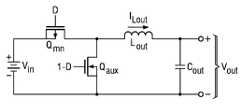
- FIG. 2illustrated is a schematic diagram of an embodiment of a power train of a power converter constructed according to the principles of the present invention. While in the illustrated embodiment, the power train employs a buck converter topology, those skilled in the art should understand that other converter topologies such as a forward converter topology are well within the broad scope of the present invention.
- the power train of the power converterreceives an input voltage V in (e.g., an unregulated input voltage) from a source of electrical power (represented by a battery) at an input thereof and provides a regulated output voltage V out to power, for instance, a microprocessor at an output of the power converter.
- V ine.g., an unregulated input voltage
- V outa regulated output voltage V out to power, for instance, a microprocessor at an output of the power converter.
- the output voltage V outis generally less than the input voltage V in such that a switching operation of the power converter can regulate the output voltage V out .
- a main switch Q mn(e.g., a P-channel MOSFET) is enabled to conduct for a primary interval (generally co-existent with a primary duty cycle “D” of the main switch Q mn ) and couples the input voltage V in to an output filter inductor L out .
- a primary intervalgenerally co-existent with a primary duty cycle “D” of the main switch Q mn
- an inductor current I Lout flowing through the output filter inductor L outincreases as a current flows from the input to the output of the power train.
- An AC component of the inductor current I Loutis filtered by the output capacitor C out .
- a complementary interval(generally co-existent with a complementary duty cycle “1-D” of the main switch Q mn )
- the main switch Q mnis transitioned to a non-conducting state and an auxiliary switch Q aux (e.g., a N-channel MOSFET) is enabled to conduct.
- the auxiliary switch Q auxprovides a path to maintain a continuity of the inductor current I Lout flowing through the output filter inductor L out .
- the inductor current I Lout through the output filter inductor L outdecreases.
- the duty cycle of the main and auxiliary switches Q mn , Q auxmay be adjusted to maintain a regulation of the output voltage V out of the power converter.
- the conduction periods for the main and auxiliary switches Q mn , Q auxmay be separated by a small time interval to avoid cross conduction therebetween and beneficially to reduce the switching losses associated with the power converter.
- the main and auxiliary switches Q mn , Q auxare embodied in P-channel and N-channel MOSFETs, respectively. Due to the design of the main switch Q mn and operating conditions of the power converter, a driver employable to provide a drive signal to control the main switch Q mn is subject to design challenges that a driver according to the present invention is adapted to overcome. Prior to introducing a driver according to the present invention, a conventional driver and the limitations associated therewith is hereinafter described.
- the totem pole drivertypically includes first and second driver switches Q DR1 , Q DR2 embodied in a P-channel MOSFET and a N-channel MOSFET, respectively, with coupled gate terminals.
- the first driver switch Q DR1is coupled to the source of electrical power for the power converter and the controller of the power converter.
- a drive signal S DRVis generated from a junction coupling the drain terminals of the first and second driver switches Q DR1 , Q DR2 of the totem pole driver.
- the drive signal S DRVWhen a signal (e.g., a pulse width modulated signal S PWM ) from the controller to the totem pole driver is high, the drive signal S DRV is essentially grounded. When the signal S PWM from the controller to the totem pole driver is low, the drive signal S DRV is substantially equal to the input Voltage V in (e.g., an unregulated input voltage) of the power converter. In effect, the drive signal S DRV from the totem pole driver exhibits voltages over the entire voltage range of the source of electrical power for the power converter.
- a signale.g., a pulse width modulated signal S PWM
- the extended voltage range present on the gate terminal of the switchmay break down the integrity of the thin gate oxide of the switch.
- the switchmay be damaged and fail.
- the switch to be drivenis referenced to another voltage (e.g., the input voltage V in to the power converter).
- the switch of the power converteris referred to as a “floating” switch.
- the totem pole driver and other presently available driversare typically not practical for applications wherein the switch to be driven exhibits a smaller control voltage limit (e.g., gate voltage limit) from the control terminal to another terminal (e.g., the gate terminal to the source terminal) thereof and is referenced to a voltage level different from the driver.
- FIG. 4illustrated is a schematic diagram of an embodiment of a driver constructed according to the principles of the present invention.
- the driveris adapted to provide a drive signal S DRV to control a switch having a control voltage limit. More specifically and in the illustrated embodiment, the driver is a gate driver that provides a gate drive signal S DRV to, for instance, a P-channel MOSFET that exhibits a gate voltage limit (i.e., a gate-to-source voltage limit) of 2.5 volts.
- the gate driverreceives a signal (e.g., a pulse width modulated signal S PWM ) from a controller (see, for instance, the controller 120 illustrated and described with respect to FIG. 1 ) and a complement of the signal (e.g., a complementary pulse width modulated signal S 1-PWM ) from the controller.
- a signale.g., a pulse width modulated signal S PWM
- the gate driverincludes switching circuitry formed by a plurality of driver switches such as first, second, third, fourth, fifth and sixth driver switches Q DR1 , Q DR2 , Q DR3 , Q DR4 , Q DR5 , Q DR6 coupled to a source of electrical power for the power converter and the controller of the power converter.
- the gate driveris also coupled to a bias voltage source that provides a bias voltage V bias , which may be internally or externally generated and may depend on an input voltage of the power converter.
- the first, second, third, fourth, fifth and sixth driver switches Q DR1 , Q DR2 , Q DR3 , Q DR4 , Q DR5 , Q DR6have a low gate voltage limit and a higher voltage drain.
- the first, second, third, fourth, fifth and sixth driver switches Q DR1 , Q DR2 , Q DR3 , Q DR4 , Q DR5 , Q DR6may exhibit a low gate voltage limit (e.g. 2.5 volts) and at the same time handle drain-to-source voltages above the gate voltage limit thereof (e.g., ten volts).
- the first, second, third, fourth, fifth and sixth driver switches Q DR1 , Q DR2 , Q DR3 , Q DR4 , Q DR5 , Q DR6exhibit a gate threshold voltage of about is 0.5 volts, which is consistent with a number of fine feature size, low voltage MOSFET designs.
- the gate threshold voltageprovides a voltage level above or below which (depending on the type) the first, second, third, fourth, fifth and sixth driver switches Q DR1 , Q DR2 , Q DR3 , Q DR4 , Q DR5 , Q DR6 are enabled to conduct.
- the first and second driver switches Q DR1 , Q DR2are N-channel MOSFETs and the third, fourth, fifth and sixth driver switches Q DR3 , Q DR4 , Q DR5 , Q DR6 are P-channel MOSFETs.
- the drain terminals of the second, third and fifth driver switches Q DR2 , Q DR3 , Q DR5are coupled together at a first node n 1 .
- the drain terminals of the first, fourth and sixth driver switches Q DR1 , Q DR4 , Q DR6are coupled together at a second node n 2 .
- each of the first, second, third, fourth, fifth and sixth driver switches Q DR1 , Q DR2 , Q DR3 , Q DR4 , Q DR5 , Q DR6are illustrated with gate, source and drain terminals, it is also common for each of the first, second, third, fourth, fifth and sixth driver switches Q DR1 , Q DR2 , Q DR3 , Q DR4 , Q DR5 , Q DR6 to include a body terminal.
- the gate driveris coupled between an input voltage V in (e.g., an unregulated input voltage at a nominal five volts) of the power converter and ground, with a potential difference therebetween for the purposes of this discussion of five volts.
- the source terminal of the third and sixth driver switches Q DR3 , Q DR6are coupled to the input voltage V in .
- the bias voltage V biasassumed for this discussion to be 2.5 volts with respect to the ground, is coupled to the gate terminal of the fourth and fifth driver switches Q DR4 , Q DR5 , and a return connection of the bias voltage source is coupled to the ground.
- the bias voltage sourcemay or may not be derived from the source of electrical power that provides the input voltage V in , depending on the application for the gate driver.
- the pulse width modulated signal S PWM provided to the second driver switch Q DR2is high (i.e., when the pulse width modulated signal S PWM is more positive than the gate threshold voltage of 0.5 volts), the first node n 1 that couples the drain terminals of the second and third driver switches Q DR2 , Q DR3 is pulled low by the second driver switch Q DR2 .
- the drain terminal of the fifth driver switch Q DR5is also coupled to the first node n 1 and the gate terminal thereof is coupled to the bias voltage source.
- the source of the fifth driver switch Q DR5is pulled down to three volts (i.e., one gate threshold voltage value more positive than the bias voltage V bias ).
- the gate drive signal S DRVis therefore pulled down two volts below the input voltage V in , which is a sufficient voltage to enable a switch such as the main switch Q mn , a P-channel MOSFET, illustrated and described with respect to the power train of the power converter of FIG. 2 to conduct.
- the first driver switch Q DR1When the complementary pulse width modulated signal S 1-PWM provided to the first driver switch Q DR1 is more positive than the gate threshold voltage, the first driver switch Q DR1 is enabled to conduct and the second node n 2 is pulled down to substantially the ground voltage by an on-resistance of the first driver switch Q DR1 .
- the gate of the third driver switch Q DR3is pulled down to about three volts (i.e., one gate threshold voltage value more positive than the bias voltage V bias ).
- the third driver switch Q DR3is enabled to conduct and the drain thereof, coupled to first node n 1 , is pulled up substantially to the input voltage V in .
- the fifth driver switch Q DR5is now enabled to conduct because the gate voltage is more than one gate threshold voltage more negative than the drain thereof, and the source of the fifth driver switch Q DR5 is pulled up substantially to the input voltage V in . Therefore, the gate drive signal S DRV from the gate driver is also pulled up to substantially the input voltage V in , which is a sufficient voltage to transition a switch such as the main switch Q mn , a P-channel MOSFET, illustrated and described with respect to the power train of the power converter of FIG. 2 to a non-conducting state.
- a type of level shifting gate driverhas been introduced with an improved level-shifting capability that can controllably raise the gate voltage of an exemplary switch (e.g., a P-channel MOSFET) to substantially the input voltage to transition the switch to a non-conducting state, and controllably reduce the gate voltage to a lower voltage to enable the switch to conduct.
- an exemplary switche.g., a P-channel MOSFET
- the gate terminal of the fifth driver switch Q DR5is coupled to the bias voltage source V bias
- the fifth driver switch Q DR5is transitioned to a non-conducting state when a voltage present on its source is less than the bias voltage V bias plus its gate threshold voltage (treating the gate threshold voltage of a P-channel MOSFET as a positive number).
- the gate driverproperly applies the bias voltage V bias (e.g., if the bias voltage V bias is the input voltage V in minus 2.5 volts and adjusted for the gate threshold voltage of the fifth driver switch Q DR5 ), the gate drive signal S DRV will not decrease more than 2.5 volts below input voltage V in thereby not exceeding the gate voltage limit of the switch to be driven.
- the bias voltage V biastherefore, is preferably dependent on the input voltage V in .
- the gate terminal of the switch(again, a P-channel MOSFET) coupled to the gate driver will thus be protected by the gate driver and, in particular, by the fifth driver switch Q DR5 , which operatively provides a protective voltage limiting function.
- the gate driveris symmetrical and as the pulse width modulated signal S PWM and complementary pulse width modulated signal S 1-PWM alternate, the conduction states and voltages within the gate driver alternate accordingly.
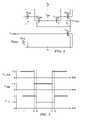
- FIG. 5illustrated are waveform diagrams demonstrating an exemplary operation of the gate driver of FIG. 4 .
- the complementary pulse width modulated signal S 1-PWMis at a voltage of 2.5 volts thereby enabling the first driver switch Q DR1 to conduct.
- the pulse width modulated signal S PWMis at zero volts at the time t 1 , which transitions the second driver switch Q DR2 to a non-conducting state.
- the gate drive signal S DRV from the gate driveris maintained at five volts thereby causing the switch such as the main switch Q mn , a P-channel MOSFET as described above, to transition to a non-conducting state.
- a polarity of the pulse width modulated signal S PWM and the complementary pulse width modulated signal S 1-PWMalternate thereby causing the second driver switch Q DR2 to transition to a conducting state and causing the first driver switch Q DR1 to transition to a non-conducting state.
- the gate drive signal S DRVdrops from five volts to 2.5 volts thereby enabling the main switch Q mn , a P-channel MOSFET as described above with a 2.5 volt gate voltage limit, to conduct.
- the brief delay period between time t 2 and time t 3represents an intrinsic delay associated with the switching action of the gate driver and may be on the order of a nanosecond.
- the gate drive signal S DRVcorrespondingly changes with the brief delay between the time t 4 and the time t 5 , which again is expected to be on the order of a nanosecond.
- the plurality of driver switches of the switching circuitry of the gate driver referenced to a voltage levelcooperate to provide the gate drive signal S DRV to a switch (e.g., the main switch Q mn , a P-channel MOSFET, of the power converter) referenced to another voltage level (in this case, the input voltage V in of the power converter).
- a switche.g., the main switch Q mn , a P-channel MOSFET, of the power converter
- the gate driveralso performs a voltage translation between the gate driver referenced to a voltage level and the switch referenced to another voltage level.
- FIG. 6illustrated is a schematic diagram of another embodiment of a driver constructed according to the principles of the present invention.
- the driveris adapted to provide a drive signal S DRV to control a switch having a control voltage limit. More specifically and in the illustrated embodiment, the driver is a gate driver that provides a gate drive signal S DRV to, for instance, a P-channel MOSFET that exhibits a gate voltage limit (i.e., a gate-to-source voltage limit) of 2.5 volts.
- the gate driverreceives a signal (e.g., a pulse width modulated signal S PWM ) from a controller (see, for instance, the controller 120 illustrated and described with respect to FIG. 1 ) and a complement of the signal (e.g., a complementary pulse width modulated signal S 1-PWM ) from the controller.
- a signale.g., a pulse width modulated signal S PWM
- the gate driverincludes switching circuitry formed by a plurality of driver switches such as first, second, third, fourth, fifth, sixth, seventh and eighth driver switches Q DR1 , Q DR2 , Q DR3 , Q DR4 , Q DR5 , Q DR6 , Q DR7 , Q DR8 coupled to a source of electrical power for the power converter and the controller of the power converter.
- the gate driveris also coupled to a first bias voltage source that provides a first bias voltage V bias1 , which may be internally or externally generated and may depend on an input voltage of the power converter.
- the first, second, third, fourth, fifth, sixth, seventh and eighth driver switches Q DR1 , Q DR2 , Q DR3 , Q DR4 , Q DR5 , Q DR6 , Q DR7 , Q DR8have a low gate voltage limit and a higher voltage drain.
- the first, second, third, fourth, fifth, sixth, seventh and eighth driver switches Q DR1 , Q DR2 , Q DR3 , Q DR4 , Q DR5 , Q DR6 , Q DR7 , Q DR8may exhibit a low gate voltage limit (e.g. 2.5 volts) and at the same time handle drain-to-source voltages above the gate voltage limit thereof (e.g., ten volts).
- the first, second, third, fourth, fifth, sixth, seventh and eighth driver switches Q DR1 , Q DR2 , Q DR3 , Q DR4 , Q DR5 , Q DR6 , Q DR7 , Q DR8exhibit a gate threshold voltage of about is 0.5 volts, which is consistent with a number of fine feature size, low voltage MOSFET designs.
- the gate threshold voltageprovides a voltage level above or below which (depending on the type) the first, second, third, fourth, fifth, sixth, seventh and eighth driver switches Q DR1 , Q DR2 , Q DR3 , Q DR4 , Q DR5 , Q DR6 , Q DR7 , Q DR8 are enabled to conduct.
- the first, second, seventh and eighth driver switches Q DR1 , Q DR2 , Q DR7 , Q DR8are N-channel MOSFETs and the third, fourth, fifth and sixth driver switches Q DR3 , Q DR4 , Q DR5 , Q DR6 are P-channel MOSFETs.
- the drain terminals of the second, third and fifth driver switches Q DR2 , Q DR3 , Q DR5are coupled together at a first node n 1 .
- the drain terminals of the first, fourth and sixth driver switches Q DR1 , Q DR4 , Q DR6are coupled together at a second node n 2 .
- each of the first, second, seventh and eighth driver switches Q DR1 , Q DR2 , Q DR7 , Q DR8are illustrated with gate, source and drain terminals, it is also common for each of the first, second, seventh and eighth driver switches Q DR1 , Q DR2 , Q DR7 , Q DR8 to include a body terminal.
- the gate driveris coupled between an input voltage V in (e.g., an unregulated input voltage at a nominal five volts) of the power converter and ground, with a potential difference therebetween for the purposes of this discussion of five volts.
- the source terminal of the third and sixth driver switches Q DR3 , Q DR6are coupled to the input voltage V in .
- the first bias voltage V bias1assumed for this discussion to be 2.5 volts with respect to the ground, is coupled to the gate terminal of the fourth and fifth driver switches Q DR4 , Q DR5 , and a return connection of the first bias voltage source is coupled to the ground.
- the first bias voltage sourcemay or may not be derived from the source of electrical power that provides the input voltage V in , depending on the application for the gate driver.
- the seventh and eighth driver switches Q DR7 , Q DR8are parallel coupled to the fourth and fifth driver switches Q DR4 , Q DR5 , respectively.
- the seventh and eighth driver switches Q DR7 , Q DR8include a higher voltage source and a higher voltage drain and typically exhibit a higher source-to-gate voltage handling (e.g., five volts) when the source is more positive than the gate and at the same time handle drain-to-source voltages above the low gate voltage limit thereof.
- the gate terminal of the seventh and eighth driver switches Q DR7 , Q DR8are coupled together and to a second voltage bias source that provides a second bias voltage V bias2 , which may be internally or externally generated and may depend on an input voltage of the power converter.
- the gate driverin the illustrated embodiment, can operate in a couple of different modes of operation. For instance, when the input voltage V in to the power converter is greater than an upper gate voltage limit for a main switch Q mn such as a P-channel MOSFET (see, as an example, the power train of the power converter illustrated and described with respect to FIG. 2 ) driven by the gate driver, then voltage protective features of the gate driver are enabled (see the description above with respect to the gate driver illustrated in FIG. 4 ). In this mode of operation, the second bias voltage V bias2 provided to the gate terminals of the seventh and eighth driver switches Q DR7 , Q DR8 is at a ground potential.
- a main switch Q mnsuch as a P-channel MOSFET
- the seventh and eighth driver switches Q DR7 , Q DR8are not coupled to a potential at or below the ground potential, the seventh and eighth driver switches Q DR7 , Q DR8 are not enabled to conduct as a consequence of the grounded gate terminals thereof. Thus, under the aforementioned circumstances, the seventh and eighth driver switches Q DR7 , Q DR8 have little effect on the operation of the gate driver.
- the input voltage V in to the power converteris not greater than an upper gate voltage limit for a main switch Q mn such as a P-channel MOSFET (see, as an example, the power train of the power converter illustrated and described with respect to FIG. 2 ) driven by the gate driver, then voltage protective features of the gate driver are not necessary.
- the clamping operation of the fifth driver switch Q DR5 on the gate drive signal S DRVis inoperative. More specifically, the gate terminal of the seventh and eighth driver switches Q DR7 , Q DR8 are coupled to a suitably high potential such as the input voltage V in .
- the seventh and eighth driver switches Q DR7 , Q DR8are enabled to conduct.
- the gate drive signal S DRVis coupled to ground potential by an on resistance of the second and eighth driver switches Q DR2 , Q DR8 when the main switch Q mn , a P-channel MOSFET as discussed above, driven by the gate driver is enabled to conduct.
- the gate drivertherefore, selectively provides additional flexibility by altering a voltage applied to an input thereof, consequently accommodating an input voltage V in above or below a gate voltage limit of a switch driven therefrom.
- FIG. 7illustrated are waveform diagrams demonstrating an exemplary operation of the gate driver of FIG. 6 .
- the gate driver described with respect to FIG. 7can operate in a couple of different modes of operation. For instance, when the input voltage V in to the power converter is greater than an upper gate voltage limit for a main switch Q mn such as a P-channel MOSFET driven by the gate driver, then voltage protective features of the gate driver are enabled. Inasmuch as the operation under such conditions is analogous to the operation of the gate driver described with respect to FIGS. 4 and 5 above, a detailed description thereof will not be forthcoming.
- the gate terminal of the seventh and eighth driver switches Q DR7 , Q DR8are coupled to the second bias voltage V bias2 , which is sufficiently near ground potential that the seventh and eighth driver switches Q DR7 , Q DR8 are not enabled to conduct and hence the operating and associated waveforms are analogous to the waveforms of FIG. 5 .
- the input voltage V in to the power converteris not greater than an upper gate voltage limit for a main switch Q mn such as a P-channel MOSFET driven by the gate driver, then voltage protective features of the gate driver are not necessary.
- the gate terminal of the seventh and eighth driver switches Q DR7 , Q DR8are coupled to the second bias voltage V bias2 , which is a suitably high potential such as the input voltage V in .
- the seventh and eighth driver switches Q DR7 , Q DR8are enabled to conduct, thereby disabling the voltage clamping operation of the fourth and fifth driver switches Q DR4 , Q DR5 .
- the gate drive signal S DRVLis substantially zero volts between the time t 3 and the time t 5 .
- the gate drive signal S DRVLis held at or below the gate voltage limit of the main switch Q mn .
- the delay between the time t 2 and time t 3 and the delay between the time t 4 and time t 5represents an intrinsic delay associated with the switching action of the gate driver and is again expected to be on the order of a nanosecond.
- the plurality of driver switches of the switching circuitry of the gate driver referenced to a voltage levelcooperate to provide the gate drive signal S DRV to a switch (e.g., the main switch Q mn , a P-channel MOSFET, of the power converter) referenced to another voltage level (in this case, the input voltage V in of the power converter).
- a switche.g., the main switch Q mn , a P-channel MOSFET, of the power converter
- the gate driveralso performs a voltage translation between the gate driver referenced to a voltage level and the switch referenced to another voltage level.
- the seventh and eighth driver switches Q DR7 , Q DR8are configured to enable a mode of operation wherein the gate drive signal S DRV for the switch is referenced to the voltage level (in this case, the ground potential) of the gate driver.
- a driver and related method of driving at least one switch of a power converterwith readily attainable and quantifiable advantages has been introduced.
- Those skilled in the artshould understand that the previously described embodiments of the driver, related method, and power converter employing the same are submitted for illustrative purposes only and that other embodiments capable of producing a drive signal for a switch referenced to different voltage levels and having a control voltage limit are well within the broad scope of the present invention.
- multiple switchesmay be included in a power converter and ones of the switches may be referenced to the same ground potential as the driver (e.g., “freewheeling switches” that can be driven with customary drivers such as the totem pole driver described above).
- a driver according to the principles of the present invention and a customary drivermay be included in the design of a power converter.
- a power converter constructed accordingly to the principles of the present inventionmay be embodied in an integrated circuit.
- portions of the power convertersuch as the driver and the power train (or portions thereof) may also be embodied in an integrated circuit and still be within the broad scope of the present invention.
- selected switches or other devices of the power convertermay be embodied in a semiconductor device as disclosed in U.S. Patent Publication No. 2005/0167756, entitled “Laterally Diffused Metal Oxide Semiconductor Device and Method of Forming the Same,” to Lotfi, et al., which is incorporated herein by reference.
- the driverincludes switching circuitry with a plurality of switches referenced to a different voltage that limit a drive signal to a switch within the control voltage limit thereof.
- the power convertercan be employed in various applications including conditions wherein the switches are subject to a low gate voltage limit.
- exemplary embodiments of the present inventionhave been illustrated with reference to specific electronic components. Those skilled in the art are aware, however, that components may be substituted (not necessarily with components of the same type) to create desired conditions or accomplish desired results. For instance, multiple components may be substituted for a single component and vice-versa.
- the principles of the present inventionmay be applied to a wide variety of power converter topologies. While the driver has been described in the environment of a power converter, those skilled in the art should understand that the driver and related principles of the present invention may be applied in other environments or applications such as a power amplifier, motor controller, and a system to control an actuator in accordance with a stepper motor or other electromechanical device.
Landscapes
- Engineering & Computer Science (AREA)
- Power Engineering (AREA)
- Power Conversion In General (AREA)
Abstract
Description
Claims (20)
Priority Applications (2)
| Application Number | Priority Date | Filing Date | Title |
|---|---|---|---|
| US10/767,540US7330017B2 (en) | 2004-01-29 | 2004-01-29 | Driver for a power converter and a method of driving a switch thereof |
| US11/961,224US7710093B2 (en) | 2004-01-29 | 2007-12-20 | Driver for a power converter and a method of driving a switch thereof |
Applications Claiming Priority (1)
| Application Number | Priority Date | Filing Date | Title |
|---|---|---|---|
| US10/767,540US7330017B2 (en) | 2004-01-29 | 2004-01-29 | Driver for a power converter and a method of driving a switch thereof |
Related Child Applications (1)
| Application Number | Title | Priority Date | Filing Date |
|---|---|---|---|
| US11/961,224ContinuationUS7710093B2 (en) | 2004-01-29 | 2007-12-20 | Driver for a power converter and a method of driving a switch thereof |
Publications (2)
| Publication Number | Publication Date |
|---|---|
| US20050168203A1 US20050168203A1 (en) | 2005-08-04 |
| US7330017B2true US7330017B2 (en) | 2008-02-12 |
Family
ID=34807688
Family Applications (2)
| Application Number | Title | Priority Date | Filing Date |
|---|---|---|---|
| US10/767,540Expired - Fee RelatedUS7330017B2 (en) | 2004-01-29 | 2004-01-29 | Driver for a power converter and a method of driving a switch thereof |
| US11/961,224Expired - Fee RelatedUS7710093B2 (en) | 2004-01-29 | 2007-12-20 | Driver for a power converter and a method of driving a switch thereof |
Family Applications After (1)
| Application Number | Title | Priority Date | Filing Date |
|---|---|---|---|
| US11/961,224Expired - Fee RelatedUS7710093B2 (en) | 2004-01-29 | 2007-12-20 | Driver for a power converter and a method of driving a switch thereof |
Country Status (1)
| Country | Link |
|---|---|
| US (2) | US7330017B2 (en) |
Cited By (52)
| Publication number | Priority date | Publication date | Assignee | Title |
|---|---|---|---|---|
| US20060096087A1 (en)* | 2004-11-10 | 2006-05-11 | Lotfi Ashraf W | Method of manufacturing a power module |
| US20060096088A1 (en)* | 2004-11-10 | 2006-05-11 | Lotfi Ashraf W | Method of manufacturing an encapsulated package for a magnetic device |
| US20070075815A1 (en)* | 2005-10-05 | 2007-04-05 | Lotfi Ashraf W | Method of forming a magnetic device having a conductive clip |
| US20070075817A1 (en)* | 2005-10-05 | 2007-04-05 | Lotfi Ashraf W | Magnetic device having a conductive clip |
| US20070074386A1 (en)* | 2005-10-05 | 2007-04-05 | Lotfi Ashraf W | Method of forming a power module with a magnetic device having a conductive clip |
| US20070075816A1 (en)* | 2005-10-05 | 2007-04-05 | Lotfi Ashraf W | Power module with a magnetic device having a conductive clip |
| US20070210777A1 (en)* | 2006-03-06 | 2007-09-13 | Cervera Pedro A | Controller for a power converter and method of operating the same |
| US20070224752A1 (en)* | 2004-01-29 | 2007-09-27 | Lotfi Ashraf W | Laterally diffused metal oxide semiconductor device and method of forming the same |
| US20080018366A1 (en)* | 2006-07-20 | 2008-01-24 | Enpirion, Inc. | Driver for switch and a method of driving the same |
| US20080094114A1 (en)* | 2006-10-20 | 2008-04-24 | Mirmira Ramarao Dwarakanath | Controller including a sawtooth generator and method of operating the same |
| US20080310189A1 (en)* | 2007-06-05 | 2008-12-18 | Saab Ab | Intergrated power converter and gate driver circuit |
| US7486060B1 (en)* | 2006-03-30 | 2009-02-03 | Western Digital Technologies, Inc. | Switching voltage regulator comprising a cycle comparator for dynamic voltage scaling |
| US20090068762A1 (en)* | 2007-09-10 | 2009-03-12 | Ken Takahashi | Methods of Processing a Substrate and Forming a Micromagnetic Device |
| US20090065363A1 (en)* | 2007-09-10 | 2009-03-12 | Liakopoulos Trifon M | Electroplating Cell and Tool |
| US20090068761A1 (en)* | 2007-09-10 | 2009-03-12 | Lotfi Ashraf W | Method of Forming a Micromagnetic Device |
| US20090066467A1 (en)* | 2007-09-10 | 2009-03-12 | Lotfi Ashraf W | Micromagnetic Device and Method of Forming the Same |
| US20090066300A1 (en)* | 2007-09-10 | 2009-03-12 | Lotfi Ashraf W | Power Converter Employing a Micromagnetic Device |
| US20090065361A1 (en)* | 2007-09-10 | 2009-03-12 | Liakopoulos Trifon M | Electrolyte and Method of Producing the Same |
| US20090068400A1 (en)* | 2007-09-10 | 2009-03-12 | Lotfi Ashraf W | Micromagnetic Device and Method of Forming the Same |
| US7551383B1 (en) | 2006-06-28 | 2009-06-23 | Western Digital Technologies, Inc. | Adjusting voltage delivered to disk drive circuitry based on a selected zone |
| US20090167267A1 (en)* | 2007-12-27 | 2009-07-02 | Mirmira Ramarao Dwarakanath | Power Converter with Monotonic Turn-On for Pre-Charged Output Capacitor |
| US20090261791A1 (en)* | 2008-04-16 | 2009-10-22 | Lopata Douglas D | Power Converter with Power Switch Operable in Controlled Current Mode |
| US20100044789A1 (en)* | 2004-01-29 | 2010-02-25 | Enpirion, Incorporated | Integrated Circuit with a Laterally Diffused Metal Oxide Semiconductor Device and Method of Forming the Same |
| US20100052050A1 (en)* | 2004-01-29 | 2010-03-04 | Enpirion, Incorporated | Integrated Circuit with a Laterally Diffused Metal Oxide Semiconductor Device and Method of Forming the Same |
| US20100052049A1 (en)* | 2004-01-29 | 2010-03-04 | Enpirion, Incorporated, A Delaware Corporation | Integrated Circuit with a Laterally Diffused Metal Oxide Semiconductor Device and Method of Forming the Same |
| US20100084750A1 (en)* | 2008-10-02 | 2010-04-08 | Lotfi Ashraf W | Module having a stacked passive element and method of forming the same |
| US20100087036A1 (en)* | 2008-10-02 | 2010-04-08 | Lotfi Ashraf W | Module having a stacked passive element and method of forming the same |
| US7733189B1 (en) | 2007-09-14 | 2010-06-08 | Western Digital Technologies, Inc. | Oscillator comprising foldover detection |
| US20100164449A1 (en)* | 2008-12-29 | 2010-07-01 | Mirmira Ramarao Dwarakanath | Power Converter with a Dynamically Configurable Controller and Output Filter |
| US20100212150A1 (en)* | 2008-10-02 | 2010-08-26 | Lotfi Ashraf W | Module Having a Stacked Magnetic Device and Semiconductor Device and Method of Forming the Same |
| US20100214746A1 (en)* | 2008-10-02 | 2010-08-26 | Lotfi Ashraf W | Module Having a Stacked Magnetic Device and Semiconductor Device and Method of Forming the Same |
| US20110049621A1 (en)* | 2004-01-29 | 2011-03-03 | Enpirion Incorporated, A Delaware Corporation | Integrated Circuit with a Laterally Diffused Metal Oxide Semiconductor Device and Method of Forming the Same |
| US20110095742A1 (en)* | 2008-04-16 | 2011-04-28 | Douglas Dean Lopata | Power Converter with Controller Operable in Selected Modes of Operation |
| US20110101933A1 (en)* | 2008-04-16 | 2011-05-05 | Douglas Dean Lopata | Power Converter with Controller Operable in Selected Modes of Operation |
| US20110101934A1 (en)* | 2008-04-16 | 2011-05-05 | Douglas Dean Lopata | Power Converter with Controller Operable in Selected Modes of Operation |
| US8018315B2 (en) | 2007-09-10 | 2011-09-13 | Enpirion, Inc. | Power converter employing a micromagnetic device |
| US8085020B1 (en) | 2008-06-13 | 2011-12-27 | Western Digital Technologies, Inc. | Switching voltage regulator employing dynamic voltage scaling with hysteretic comparator |
| US8133529B2 (en) | 2007-09-10 | 2012-03-13 | Enpirion, Inc. | Method of forming a micromagnetic device |
| US8253195B2 (en) | 2004-01-29 | 2012-08-28 | Enpirion, Inc. | Integrated circuit with a laterally diffused metal oxide semiconductor device and method of forming the same |
| US8253196B2 (en) | 2004-01-29 | 2012-08-28 | Enpirion, Inc. | Integrated circuit with a laterally diffused metal oxide semiconductor device and method of forming the same |
| US8686698B2 (en) | 2008-04-16 | 2014-04-01 | Enpirion, Inc. | Power converter with controller operable in selected modes of operation |
| US8867295B2 (en) | 2010-12-17 | 2014-10-21 | Enpirion, Inc. | Power converter for a memory module |
| US9246390B2 (en) | 2008-04-16 | 2016-01-26 | Enpirion, Inc. | Power converter with controller operable in selected modes of operation |
| US9299691B2 (en) | 2012-11-30 | 2016-03-29 | Enpirion, Inc. | Semiconductor device including alternating source and drain regions, and respective source and drain metallic strips |
| US9509217B2 (en) | 2015-04-20 | 2016-11-29 | Altera Corporation | Asymmetric power flow controller for a power converter and method of operating the same |
| US9536938B1 (en) | 2013-11-27 | 2017-01-03 | Altera Corporation | Semiconductor device including a resistor metallic layer and method of forming the same |
| US9548714B2 (en) | 2008-12-29 | 2017-01-17 | Altera Corporation | Power converter with a dynamically configurable controller and output filter |
| US9673192B1 (en) | 2013-11-27 | 2017-06-06 | Altera Corporation | Semiconductor device including a resistor metallic layer and method of forming the same |
| US9673135B2 (en) | 2014-01-13 | 2017-06-06 | Altera Corporation | Semiconductor device having mirror-symmetric terminals and methods of forming the same |
| US10020739B2 (en) | 2014-03-27 | 2018-07-10 | Altera Corporation | Integrated current replicator and method of operating the same |
| US10103627B2 (en) | 2015-02-26 | 2018-10-16 | Altera Corporation | Packaged integrated circuit including a switch-mode regulator and method of forming the same |
| US20210250021A1 (en)* | 2018-08-28 | 2021-08-12 | Texas Instruments Incorporated | Methods and apparatus to transmit signals in isolated gate drivers |
Families Citing this family (20)
| Publication number | Priority date | Publication date | Assignee | Title |
|---|---|---|---|---|
| US7190026B2 (en)* | 2004-08-23 | 2007-03-13 | Enpirion, Inc. | Integrated circuit employable with a power converter |
| US7195981B2 (en) | 2004-08-23 | 2007-03-27 | Enpirion, Inc. | Method of forming an integrated circuit employable with a power converter |
| US7229886B2 (en) | 2004-08-23 | 2007-06-12 | Enpirion, Inc. | Method of forming an integrated circuit incorporating higher voltage devices and low voltage devices therein |
| US7335948B2 (en)* | 2004-08-23 | 2008-02-26 | Enpirion, Inc. | Integrated circuit incorporating higher voltage devices and low voltage devices therein |
| US7015544B2 (en)* | 2004-08-23 | 2006-03-21 | Enpirion, Inc. | Intergrated circuit employable with a power converter |
| US7214985B2 (en)* | 2004-08-23 | 2007-05-08 | Enpirion, Inc. | Integrated circuit incorporating higher voltage devices and low voltage devices therein |
| US7186606B2 (en)* | 2004-08-23 | 2007-03-06 | Enpirion, Inc. | Method of forming an integrated circuit employable with a power converter |
| US7864546B2 (en)* | 2007-02-13 | 2011-01-04 | Akros Silicon Inc. | DC-DC converter with communication across an isolation pathway |
| US7923710B2 (en) | 2007-03-08 | 2011-04-12 | Akros Silicon Inc. | Digital isolator with communication across an isolation barrier |
| US7701731B2 (en) | 2007-02-13 | 2010-04-20 | Akros Silicon Inc. | Signal communication across an isolation barrier |
| US20080181316A1 (en)* | 2007-01-25 | 2008-07-31 | Philip John Crawley | Partitioned Signal and Power Transfer Across an Isolation Barrier |
| US20100054001A1 (en)* | 2008-08-26 | 2010-03-04 | Kenneth Dyer | AC/DC Converter with Power Factor Correction |
| KR101606400B1 (en)* | 2008-12-30 | 2016-03-25 | 주식회사 동부하이텍 | High Speed Differential Level Shifter and the Boot Strap Driver including the same |
| FI122206B (en)* | 2009-06-30 | 2011-10-14 | Vacon Oyj | Power Transmission Method and Equipment |
| US8487598B2 (en)* | 2010-08-30 | 2013-07-16 | Texas Instruments Incorporated | DC-DC converter with unity-gain feedback amplifier driving bias transistor |
| US9059641B2 (en)* | 2011-07-05 | 2015-06-16 | Atmel Corporation | Main supply zero crossing detection for PFC converter |
| US9154026B2 (en) | 2012-06-27 | 2015-10-06 | Intel Corporation | Bridge driver for a switching voltage regulator which is operable to soft-switch and hard-switch |
| US9118249B2 (en)* | 2012-07-27 | 2015-08-25 | Excelliance Mos Corporation | Power conversion apparatus |
| JP2015186360A (en)* | 2014-03-25 | 2015-10-22 | 株式会社日立製作所 | Power converter, machine equipped with power converter |
| CN106464152B (en)* | 2014-05-09 | 2019-07-26 | 松下知识产权经营株式会社 | Rectifier circuit and non-contact power supply device |
Citations (33)
| Publication number | Priority date | Publication date | Assignee | Title |
|---|---|---|---|---|
| US4761725A (en) | 1986-08-01 | 1988-08-02 | Unisys Corporation | Digitally controlled A.C. to D.C. power conditioner |
| US4912622A (en)* | 1988-03-07 | 1990-03-27 | General Electric Company | Gate driver for a full-bridge lossless switching device |
| US4982353A (en) | 1989-09-28 | 1991-01-01 | General Electric Company | Subsampling time-domain digital filter using sparsely clocked output latch |
| US5245228A (en)* | 1991-03-22 | 1993-09-14 | Siemens Aktiengesellschaft | Level inverter circuit |
| US5258662A (en)* | 1992-04-06 | 1993-11-02 | Linear Technology Corp. | Micropower gate charge pump for power MOSFETS |
| US5285369A (en) | 1992-09-01 | 1994-02-08 | Power Integrations, Inc. | Switched mode power supply integrated circuit with start-up self-biasing |
| US5371415A (en)* | 1993-06-21 | 1994-12-06 | Motorola, Inc. | Two stage gate drive circuit for a FET |
| US5469334A (en) | 1991-09-09 | 1995-11-21 | Power Integrations, Inc. | Plastic quad-packaged switched-mode integrated circuit with integrated transformer windings and mouldings for transformer core pieces |
| US5594324A (en) | 1995-03-31 | 1997-01-14 | Space Systems/Loral, Inc. | Stabilized power converter having quantized duty cycle |
| US5689213A (en) | 1995-08-23 | 1997-11-18 | Micron Technology, Inc. | Post-fabrication programmable integrated circuit ring oscillator |
| US5796276A (en)* | 1994-12-30 | 1998-08-18 | Sgs-Thomson Microelectronics, Inc. | High-side-driver gate drive circuit |
| US5877611A (en)* | 1996-10-09 | 1999-03-02 | Lucent Technologies Inc. | Simple and efficient switching regulator for fast transient loads such as microprocessors |
| US5977811A (en)* | 1996-07-16 | 1999-11-02 | Stmicroelectronics S.R.L. | Shift level circuit for a high side driver circuit |
| US6005377A (en) | 1997-09-17 | 1999-12-21 | Lucent Technologies Inc. | Programmable digital controller for switch mode power conversion and power supply employing the same |
| US6118351A (en) | 1997-06-10 | 2000-09-12 | Lucent Technologies Inc. | Micromagnetic device for power processing applications and method of manufacture therefor |
| US6201429B1 (en)* | 1999-05-20 | 2001-03-13 | Analog Microelectronics, Inc. | Clamped cascode level shifter circuit |
| US6255714B1 (en) | 1999-06-22 | 2001-07-03 | Agere Systems Guardian Corporation | Integrated circuit having a micromagnetic device including a ferromagnetic core and method of manufacture therefor |
| US6262564B1 (en)* | 2000-11-10 | 2001-07-17 | Lucent Technologies Inc. | Driver for a controllable switch in a power converter |
| US6285539B1 (en)* | 1999-07-13 | 2001-09-04 | Mitsubishi Denki Kabushiki Kaisha | Switch driver |
| US6320449B1 (en)* | 1999-10-22 | 2001-11-20 | Stmicroelectronics S.R.L. | Driver circuit for P-channel MOS switches |
| US6388468B1 (en)* | 2000-08-30 | 2002-05-14 | Yazaki North America | Circuit and method for operating a MOSFET control circuit with a system operating voltage greater than a maximum supply voltage limit |
| US6407594B1 (en)* | 1993-04-09 | 2002-06-18 | Sgs-Thomson Microelectronics S.R.L. | Zero bias current driver control circuit |
| US6407579B1 (en)* | 2000-01-20 | 2002-06-18 | Koninklijke Philips Electronics N.V. | Fast high voltage level shifter with gate oxide protection |
| US6477065B2 (en)* | 1994-10-31 | 2002-11-05 | Texas Instruments Incorporated | Resonant gate driver |
| US20020175661A1 (en)* | 2001-02-06 | 2002-11-28 | Koninklijke Philips Electronics N.V. | Integrated FET and driver |
| US6495019B1 (en) | 2000-04-19 | 2002-12-17 | Agere Systems Inc. | Device comprising micromagnetic components for power applications and process for forming device |
| US6541819B2 (en) | 2001-05-24 | 2003-04-01 | Agere Systems Inc. | Semiconductor device having non-power enhanced and power enhanced metal oxide semiconductor devices and a method of manufacture therefor |
| US6573694B2 (en)* | 2001-06-27 | 2003-06-03 | Texas Instruments Incorporated | Stable low dropout, low impedance driver for linear regulators |
| US6639427B2 (en)* | 2000-11-29 | 2003-10-28 | Stmicroelectronics Sa | High-voltage switching device and application to a non-volatile memory |
| US6650169B2 (en)* | 2001-10-01 | 2003-11-18 | Koninklijke Philips Electronics N.V. | Gate driver apparatus having an energy recovering circuit |
| US6791305B2 (en) | 2002-02-28 | 2004-09-14 | Tdk Corporation | Switching power supply control circuit and switching power supply using same |
| US6822882B1 (en)* | 2003-08-01 | 2004-11-23 | Tyco Electronics Power Systems, Inc. | Gate driver with a DC offset bias circuit and a power converter employing the same |
| US6879137B2 (en)* | 2002-06-17 | 2005-04-12 | Hitachi, Ltd. | Power-supply device |
Family Cites Families (35)
| Publication number | Priority date | Publication date | Assignee | Title |
|---|---|---|---|---|
| US4553044A (en)* | 1983-05-11 | 1985-11-12 | National Semiconductor Corporation | Integrated circuit output driver stage |
| US4654770A (en)* | 1983-12-22 | 1987-03-31 | General Electric Company | Current-limit circuit in X-ray generator |
| IT1215369B (en)* | 1987-02-25 | 1990-02-08 | Sgs Microelettronica Spa | PERIODIC SIGNAL GENERATOR WITH EXPONENTIAL TREND, IN PARTICULAR FOR SWITCHING POWER SUPPLIES. |
| US5481178A (en)* | 1993-03-23 | 1996-01-02 | Linear Technology Corporation | Control circuit and method for maintaining high efficiency over broad current ranges in a switching regulator circuit |
| US5414341A (en)* | 1993-12-07 | 1995-05-09 | Benchmarq Microelectronics, Inc. | DC-DC converter operable in an asyncronous or syncronous or linear mode |
| US5510739A (en)* | 1994-03-28 | 1996-04-23 | Motorola, Inc. | Circuit and method for enhancing logic transitions appearing on a line |
| JP3123349B2 (en)* | 1994-06-29 | 2001-01-09 | 富士電機株式会社 | Control circuit for semiconductor device |
| US5568044A (en)* | 1994-09-27 | 1996-10-22 | Micrel, Inc. | Voltage regulator that operates in either PWM or PFM mode |
| US5541541A (en)* | 1994-11-23 | 1996-07-30 | Texas Instruments Incorporated | Comparator circuit for decreasing shoot-through current on power switches |
| JP2896342B2 (en)* | 1995-05-04 | 1999-05-31 | インターナショナル・レクチファイヤー・コーポレーション | Method and circuit for driving a plurality of power transistors in a half-wave bridge configuration and allowing excessive negative oscillation of an output node, and an integrated circuit incorporating the circuit |
| US5502412A (en)* | 1995-05-04 | 1996-03-26 | International Rectifier Corporation | Method and circuit for driving power transistors in a half bridge configuration from control signals referenced to any potential between the line voltage and the line voltage return and integrated circuit incorporating the circuit |
| US5688213A (en)* | 1996-10-11 | 1997-11-18 | Recker; Mark I. | Exercise apparatus |
| US5864225A (en)* | 1997-06-04 | 1999-01-26 | Fairchild Semiconductor Corporation | Dual adjustable voltage regulators |
| JP3152204B2 (en)* | 1998-06-02 | 2001-04-03 | 日本電気株式会社 | Slew rate output circuit |
| JP2000091902A (en)* | 1998-09-16 | 2000-03-31 | Nec Corp | Interface circuit and input buffer integrated circuit including it |
| US6169433B1 (en)* | 1999-01-14 | 2001-01-02 | National Semiconductor Corporation | Method and apparatus using feedback to generate a ramped voltage with controlled maximum amplitude |
| JP3736227B2 (en)* | 1999-09-20 | 2006-01-18 | 富士電機デバイステクノロジー株式会社 | Drive circuit |
| US6759692B1 (en)* | 2002-02-04 | 2004-07-06 | Ixys Corporation | Gate driver with level shift circuit |
| JP3637904B2 (en)* | 2002-07-24 | 2005-04-13 | セイコーエプソン株式会社 | Power circuit |
| US6828825B2 (en)* | 2002-08-27 | 2004-12-07 | Texas Instruments Incorporated | Pulse response of fast level shifter |
| US6922044B2 (en)* | 2002-09-06 | 2005-07-26 | Intersil Americas Inc. | Synchronization of multiphase synthetic ripple voltage regulator |
| US7602167B2 (en)* | 2003-01-06 | 2009-10-13 | Texas Instruments Incorporated | Reconfigurable topology for switching and linear voltage regulators |
| US6922041B2 (en) | 2003-02-28 | 2005-07-26 | Sipex Corporation | Apparatus for and method of adjusting a switching regulator output for a circuit having a pre-charge voltage |
| US7038514B2 (en) | 2003-10-28 | 2006-05-02 | Intersil Americas Inc. | Startup circuit for a DC-DC converter |
| US7061217B2 (en)* | 2004-01-28 | 2006-06-13 | Texas Instruments Deutschland, Gmbh | Integrated power switching circuit |
| US7230302B2 (en) | 2004-01-29 | 2007-06-12 | Enpirion, Inc. | Laterally diffused metal oxide semiconductor device and method of forming the same |
| US7038438B2 (en) | 2004-01-29 | 2006-05-02 | Enpirion, Inc. | Controller for a power converter and a method of controlling a switch thereof |
| US7019505B2 (en) | 2004-01-29 | 2006-03-28 | Enpirion, Inc. | Digital controller for a power converter employing selectable phases of a clock signal |
| US7015544B2 (en) | 2004-08-23 | 2006-03-21 | Enpirion, Inc. | Intergrated circuit employable with a power converter |
| US7214985B2 (en) | 2004-08-23 | 2007-05-08 | Enpirion, Inc. | Integrated circuit incorporating higher voltage devices and low voltage devices therein |
| TWI276937B (en)* | 2004-12-20 | 2007-03-21 | Ind Tech Res Inst | Bias voltage generator with automatic slew rate adjustment |
| US7521907B2 (en)* | 2006-03-06 | 2009-04-21 | Enpirion, Inc. | Controller for a power converter and method of operating the same |
| US7893676B2 (en)* | 2006-07-20 | 2011-02-22 | Enpirion, Inc. | Driver for switch and a method of driving the same |
| US7948280B2 (en)* | 2006-10-20 | 2011-05-24 | Enpirion, Inc. | Controller including a sawtooth generator and method of operating the same |
| US7876080B2 (en)* | 2007-12-27 | 2011-01-25 | Enpirion, Inc. | Power converter with monotonic turn-on for pre-charged output capacitor |
- 2004
- 2004-01-29USUS10/767,540patent/US7330017B2/ennot_activeExpired - Fee Related
- 2007
- 2007-12-20USUS11/961,224patent/US7710093B2/ennot_activeExpired - Fee Related
Patent Citations (33)
| Publication number | Priority date | Publication date | Assignee | Title |
|---|---|---|---|---|
| US4761725A (en) | 1986-08-01 | 1988-08-02 | Unisys Corporation | Digitally controlled A.C. to D.C. power conditioner |
| US4912622A (en)* | 1988-03-07 | 1990-03-27 | General Electric Company | Gate driver for a full-bridge lossless switching device |
| US4982353A (en) | 1989-09-28 | 1991-01-01 | General Electric Company | Subsampling time-domain digital filter using sparsely clocked output latch |
| US5245228A (en)* | 1991-03-22 | 1993-09-14 | Siemens Aktiengesellschaft | Level inverter circuit |
| US5469334A (en) | 1991-09-09 | 1995-11-21 | Power Integrations, Inc. | Plastic quad-packaged switched-mode integrated circuit with integrated transformer windings and mouldings for transformer core pieces |
| US5258662A (en)* | 1992-04-06 | 1993-11-02 | Linear Technology Corp. | Micropower gate charge pump for power MOSFETS |
| US5285369A (en) | 1992-09-01 | 1994-02-08 | Power Integrations, Inc. | Switched mode power supply integrated circuit with start-up self-biasing |
| US6407594B1 (en)* | 1993-04-09 | 2002-06-18 | Sgs-Thomson Microelectronics S.R.L. | Zero bias current driver control circuit |
| US5371415A (en)* | 1993-06-21 | 1994-12-06 | Motorola, Inc. | Two stage gate drive circuit for a FET |
| US6477065B2 (en)* | 1994-10-31 | 2002-11-05 | Texas Instruments Incorporated | Resonant gate driver |
| US5796276A (en)* | 1994-12-30 | 1998-08-18 | Sgs-Thomson Microelectronics, Inc. | High-side-driver gate drive circuit |
| US5594324A (en) | 1995-03-31 | 1997-01-14 | Space Systems/Loral, Inc. | Stabilized power converter having quantized duty cycle |
| US5689213A (en) | 1995-08-23 | 1997-11-18 | Micron Technology, Inc. | Post-fabrication programmable integrated circuit ring oscillator |
| US5977811A (en)* | 1996-07-16 | 1999-11-02 | Stmicroelectronics S.R.L. | Shift level circuit for a high side driver circuit |
| US5877611A (en)* | 1996-10-09 | 1999-03-02 | Lucent Technologies Inc. | Simple and efficient switching regulator for fast transient loads such as microprocessors |
| US6118351A (en) | 1997-06-10 | 2000-09-12 | Lucent Technologies Inc. | Micromagnetic device for power processing applications and method of manufacture therefor |
| US6005377A (en) | 1997-09-17 | 1999-12-21 | Lucent Technologies Inc. | Programmable digital controller for switch mode power conversion and power supply employing the same |
| US6201429B1 (en)* | 1999-05-20 | 2001-03-13 | Analog Microelectronics, Inc. | Clamped cascode level shifter circuit |
| US6255714B1 (en) | 1999-06-22 | 2001-07-03 | Agere Systems Guardian Corporation | Integrated circuit having a micromagnetic device including a ferromagnetic core and method of manufacture therefor |
| US6285539B1 (en)* | 1999-07-13 | 2001-09-04 | Mitsubishi Denki Kabushiki Kaisha | Switch driver |
| US6320449B1 (en)* | 1999-10-22 | 2001-11-20 | Stmicroelectronics S.R.L. | Driver circuit for P-channel MOS switches |
| US6407579B1 (en)* | 2000-01-20 | 2002-06-18 | Koninklijke Philips Electronics N.V. | Fast high voltage level shifter with gate oxide protection |
| US6495019B1 (en) | 2000-04-19 | 2002-12-17 | Agere Systems Inc. | Device comprising micromagnetic components for power applications and process for forming device |
| US6388468B1 (en)* | 2000-08-30 | 2002-05-14 | Yazaki North America | Circuit and method for operating a MOSFET control circuit with a system operating voltage greater than a maximum supply voltage limit |
| US6262564B1 (en)* | 2000-11-10 | 2001-07-17 | Lucent Technologies Inc. | Driver for a controllable switch in a power converter |
| US6639427B2 (en)* | 2000-11-29 | 2003-10-28 | Stmicroelectronics Sa | High-voltage switching device and application to a non-volatile memory |
| US20020175661A1 (en)* | 2001-02-06 | 2002-11-28 | Koninklijke Philips Electronics N.V. | Integrated FET and driver |
| US6541819B2 (en) | 2001-05-24 | 2003-04-01 | Agere Systems Inc. | Semiconductor device having non-power enhanced and power enhanced metal oxide semiconductor devices and a method of manufacture therefor |
| US6573694B2 (en)* | 2001-06-27 | 2003-06-03 | Texas Instruments Incorporated | Stable low dropout, low impedance driver for linear regulators |
| US6650169B2 (en)* | 2001-10-01 | 2003-11-18 | Koninklijke Philips Electronics N.V. | Gate driver apparatus having an energy recovering circuit |
| US6791305B2 (en) | 2002-02-28 | 2004-09-14 | Tdk Corporation | Switching power supply control circuit and switching power supply using same |
| US6879137B2 (en)* | 2002-06-17 | 2005-04-12 | Hitachi, Ltd. | Power-supply device |
| US6822882B1 (en)* | 2003-08-01 | 2004-11-23 | Tyco Electronics Power Systems, Inc. | Gate driver with a DC offset bias circuit and a power converter employing the same |
Non-Patent Citations (14)
| Title |
|---|
| "Linear Technology: LTC3736-1: Dual 2-Phase, No R<SUB>SENSE</SUB>(TM), Synchronous Controller with Spread Spectrum," 2004, 28 pp., Linear Technology Corporation, Milpitas, CA. |
| "TPS40100: Midrange Input Synchronous Buck Controller with Advanced Sequencing and Output Margining," May 2005, 37 pp., Texas Instruments Incorporated, Dallas, TX. |
| Barrado, A., et al., "New DC/DC Converter with Low Output Voltage and Fast Transient Response," Proceedings of the IEEE Applied Power Electronics Conference, 2003, pp. 432-437, IEEE, Los Alamitos, CA. |
| Betancourt-Zamora, R.J. et al., "A 1.5 mW, 200 MHz CMOS VCO for Wireless Biotelemetry," First International Workshop on Design of Mixed-Mode Integrated Circuits and Applications, Cancun, Mexico, pp. 72-74, Jul., 1997. |
| Goder, D., et al., "V<SUP>2 </SUP>Architecture Provides Ultra-Fast Transient Response in Switch Mode Power Supplies," Proceedings of HFPC Power Conversion, 1996, pp. 414-420. |
| Goodman, J. et al., "An Energy/Security Scalable Encryption Processor Using an Embedded Variable Voltage DC/DC Converter," IEEE Journal of Solid-State Circuits, vol. 33, No. 11 (Nov. 1998). |
| Horowitz, P., et al., "The Art of Electronics," Second Edition, 1989, pp. 288-291, Cambridge University Press, Cambridge, MA. |
| Lotfi, A.W., et al., "Issues and Advances in High-Frequency Magnetics for Switching Power Supplies," Proceedings of the IEEE, Jun. 2001, vol. 89, No. 6, pp. 833-845. |
| Patella, B.J., et al., "High-Frequency Digital Controller IC for DC/DC Converters," IEEE Proceedings of the Applied Power Electronics Conference, Mar. 10, 2002, 7 pp., IEEE, Los Alamitos, CA. |
| Peterchev, A.V., et al., "Quantization Resolution and Limit Cycling in Digitally Controlled PWM Converters," IEEE Transactions on Power Electronics, Jan. 2003, pp. 301-303, vol. 18, No. 1, IEEE, Los Alamitos, CA. |
| Redl, R., et al., "Optimizing the Load Transient Response of the Buck Converter," Proceedings of the IEEE Applied Power Electronics Conference, 1998, pp. 170-176, IEEE, Los Alamitos, CA. |
| Schoneman, G.K., et al., "Output Impedance Considerations for Switching Regulators with Current-Injected Control," Proceedings of the 18th Annual IEEE Power Electronics Specialists Conference, Jun. 1987, pp. 324-335, IEEE, Los Alamitos, CA. |
| Soto, A., et al. "Analysis of the Buck Converter for Scaling the Supply Voltage of Digital Circuits," Proceedings of the IEEE Applied Power Electronics Conference, 2003, pp. 711-717, IEEE, Los Alamitos, CA. |
| Soto, A., et al., "Design Methodology for Dynamic Voltage Scaling in the Buck Converter," Proceedings of the IEEE Applied Power Electronics Conferece, 2005, pp. 263-269, IEEE, Los Alamitos, CA. |
Cited By (115)
| Publication number | Priority date | Publication date | Assignee | Title |
|---|---|---|---|---|
| US8633540B2 (en) | 2004-01-29 | 2014-01-21 | Enpirion, Inc. | Integrated circuit with a laterally diffused metal oxide semiconductor device and method of forming the same |
| US8212317B2 (en) | 2004-01-29 | 2012-07-03 | Enpirion, Inc. | Integrated circuit with a laterally diffused metal oxide semiconductor device and method of forming the same |
| US7759184B2 (en) | 2004-01-29 | 2010-07-20 | Enpirion, Inc. | Laterally diffused metal oxide semiconductor device and method of forming the same |
| US20110049621A1 (en)* | 2004-01-29 | 2011-03-03 | Enpirion Incorporated, A Delaware Corporation | Integrated Circuit with a Laterally Diffused Metal Oxide Semiconductor Device and Method of Forming the Same |
| US20100052049A1 (en)* | 2004-01-29 | 2010-03-04 | Enpirion, Incorporated, A Delaware Corporation | Integrated Circuit with a Laterally Diffused Metal Oxide Semiconductor Device and Method of Forming the Same |
| US20100052050A1 (en)* | 2004-01-29 | 2010-03-04 | Enpirion, Incorporated | Integrated Circuit with a Laterally Diffused Metal Oxide Semiconductor Device and Method of Forming the Same |
| US20100044789A1 (en)* | 2004-01-29 | 2010-02-25 | Enpirion, Incorporated | Integrated Circuit with a Laterally Diffused Metal Oxide Semiconductor Device and Method of Forming the Same |
| US20070224752A1 (en)* | 2004-01-29 | 2007-09-27 | Lotfi Ashraf W | Laterally diffused metal oxide semiconductor device and method of forming the same |
| US20070284658A1 (en)* | 2004-01-29 | 2007-12-13 | Lotfi Ashraf W | Laterally Diffused Metal Oxide Semiconductor Device and Method of Forming the Same |
| US9680008B2 (en) | 2004-01-29 | 2017-06-13 | Empirion, Inc. | Laterally diffused metal oxide semiconductor device and method of forming the same |
| US8987815B2 (en) | 2004-01-29 | 2015-03-24 | Enpirion, Inc. | Integrated circuit with a laterally diffused metal oxide semiconductor device and method of forming the same |
| US8212316B2 (en) | 2004-01-29 | 2012-07-03 | Enpirion, Inc. | Integrated circuit with a laterally diffused metal oxide semiconductor device and method of forming the same |
| US8212315B2 (en) | 2004-01-29 | 2012-07-03 | Enpirion, Inc. | Integrated circuit with a laterally diffused metal oxide semiconductor device and method of forming the same |
| US8716790B2 (en) | 2004-01-29 | 2014-05-06 | Enpirion, Inc. | Laterally diffused metal oxide semiconductor device and method of forming the same |
| US8253195B2 (en) | 2004-01-29 | 2012-08-28 | Enpirion, Inc. | Integrated circuit with a laterally diffused metal oxide semiconductor device and method of forming the same |
| US8253196B2 (en) | 2004-01-29 | 2012-08-28 | Enpirion, Inc. | Integrated circuit with a laterally diffused metal oxide semiconductor device and method of forming the same |
| US8253197B2 (en) | 2004-01-29 | 2012-08-28 | Enpirion, Inc. | Integrated circuit with a laterally diffused metal oxide semiconductor device and method of forming the same |
| US8528190B2 (en) | 2004-11-10 | 2013-09-10 | Enpirion, Inc. | Method of manufacturing a power module |
| US8043544B2 (en) | 2004-11-10 | 2011-10-25 | Enpirion, Inc. | Method of manufacturing an encapsulated package for a magnetic device |
| US20060096087A1 (en)* | 2004-11-10 | 2006-05-11 | Lotfi Ashraf W | Method of manufacturing a power module |
| US20060096088A1 (en)* | 2004-11-10 | 2006-05-11 | Lotfi Ashraf W | Method of manufacturing an encapsulated package for a magnetic device |
| US20090065964A1 (en)* | 2004-11-10 | 2009-03-12 | Lotfi Ashraf W | Method of Manufacturing an Encapsulated Package for a Magnetic Device |
| US7426780B2 (en) | 2004-11-10 | 2008-09-23 | Enpirion, Inc. | Method of manufacturing a power module |
| US7462317B2 (en) | 2004-11-10 | 2008-12-09 | Enpirion, Inc. | Method of manufacturing an encapsulated package for a magnetic device |
| US8139362B2 (en) | 2005-10-05 | 2012-03-20 | Enpirion, Inc. | Power module with a magnetic device having a conductive clip |
| US8701272B2 (en) | 2005-10-05 | 2014-04-22 | Enpirion, Inc. | Method of forming a power module with a magnetic device having a conductive clip |
| US8631560B2 (en) | 2005-10-05 | 2014-01-21 | Enpirion, Inc. | Method of forming a magnetic device having a conductive clip |
| US20100176905A1 (en)* | 2005-10-05 | 2010-07-15 | Lotfi Ashraf W | Magnetic Device Having a Conductive Clip |
| US8384506B2 (en) | 2005-10-05 | 2013-02-26 | Enpirion, Inc. | Magnetic device having a conductive clip |
| US10304615B2 (en) | 2005-10-05 | 2019-05-28 | Enpirion, Inc. | Method of forming a power module with a magnetic device having a conductive clip |
| US20070075816A1 (en)* | 2005-10-05 | 2007-04-05 | Lotfi Ashraf W | Power module with a magnetic device having a conductive clip |
| US20070074386A1 (en)* | 2005-10-05 | 2007-04-05 | Lotfi Ashraf W | Method of forming a power module with a magnetic device having a conductive clip |
| US20070075817A1 (en)* | 2005-10-05 | 2007-04-05 | Lotfi Ashraf W | Magnetic device having a conductive clip |
| US7688172B2 (en) | 2005-10-05 | 2010-03-30 | Enpirion, Inc. | Magnetic device having a conductive clip |
| US20070075815A1 (en)* | 2005-10-05 | 2007-04-05 | Lotfi Ashraf W | Method of forming a magnetic device having a conductive clip |
| US20090212751A1 (en)* | 2006-03-06 | 2009-08-27 | Pedro Alou Cervera | Controller for a Power Converter and Method of Operating The Same |
| US20070210777A1 (en)* | 2006-03-06 | 2007-09-13 | Cervera Pedro A | Controller for a power converter and method of operating the same |
| US9748840B2 (en) | 2006-03-06 | 2017-08-29 | Altera Corporation | Controller for a power converter and method of operating the same |
| US8013580B2 (en) | 2006-03-06 | 2011-09-06 | Enpirion, Inc. | Controller for a power converter and method of operating the same |
| US8736241B2 (en) | 2006-03-06 | 2014-05-27 | Enpirion, Inc. | Controller for a power converter and method of operating the same |
| US7521907B2 (en) | 2006-03-06 | 2009-04-21 | Enpirion, Inc. | Controller for a power converter and method of operating the same |
| US7486060B1 (en)* | 2006-03-30 | 2009-02-03 | Western Digital Technologies, Inc. | Switching voltage regulator comprising a cycle comparator for dynamic voltage scaling |
| US8912778B1 (en) | 2006-03-30 | 2014-12-16 | Western Digital Technologies, Inc. | Switching voltage regulator employing current pre-adjust based on power mode |
| US7551383B1 (en) | 2006-06-28 | 2009-06-23 | Western Digital Technologies, Inc. | Adjusting voltage delivered to disk drive circuitry based on a selected zone |
| US20080018366A1 (en)* | 2006-07-20 | 2008-01-24 | Enpirion, Inc. | Driver for switch and a method of driving the same |
| US7893676B2 (en) | 2006-07-20 | 2011-02-22 | Enpirion, Inc. | Driver for switch and a method of driving the same |
| US20080094114A1 (en)* | 2006-10-20 | 2008-04-24 | Mirmira Ramarao Dwarakanath | Controller including a sawtooth generator and method of operating the same |
| US7948280B2 (en) | 2006-10-20 | 2011-05-24 | Enpirion, Inc. | Controller including a sawtooth generator and method of operating the same |
| US20080310189A1 (en)* | 2007-06-05 | 2008-12-18 | Saab Ab | Intergrated power converter and gate driver circuit |
| US7952340B2 (en)* | 2007-06-05 | 2011-05-31 | Saab Ab | Integrated power converter and gate driver circuit |
| US7955868B2 (en) | 2007-09-10 | 2011-06-07 | Enpirion, Inc. | Method of forming a micromagnetic device |
| US20090065363A1 (en)* | 2007-09-10 | 2009-03-12 | Liakopoulos Trifon M | Electroplating Cell and Tool |
| US9611561B2 (en) | 2007-09-10 | 2017-04-04 | Enpirion, Inc. | Electroplating cell and tool |
| US7952459B2 (en) | 2007-09-10 | 2011-05-31 | Enpirion, Inc. | Micromagnetic device and method of forming the same |
| US9299489B2 (en) | 2007-09-10 | 2016-03-29 | Enpirion, Inc. | Micromagnetic device and method of forming the same |
| US20090068762A1 (en)* | 2007-09-10 | 2009-03-12 | Ken Takahashi | Methods of Processing a Substrate and Forming a Micromagnetic Device |
| US20110181383A1 (en)* | 2007-09-10 | 2011-07-28 | Lotfi Ashraf W | Micromagnetic Device and Method of Forming the Same |
| US8002961B2 (en) | 2007-09-10 | 2011-08-23 | Enpirion, Inc. | Electrolyte and method of producing the same |
| US7943510B2 (en) | 2007-09-10 | 2011-05-17 | Enpirion, Inc. | Methods of processing a substrate and forming a micromagnetic device |
| US20110217793A1 (en)* | 2007-09-10 | 2011-09-08 | Ken Takahashi | Methods of Processing a Substrate and Forming a Micromagnetic Device |
| US8018315B2 (en) | 2007-09-10 | 2011-09-13 | Enpirion, Inc. | Power converter employing a micromagnetic device |
| US8618900B2 (en) | 2007-09-10 | 2013-12-31 | Enpirion, Inc. | Micromagnetic device and method of forming the same |
| US20090068761A1 (en)* | 2007-09-10 | 2009-03-12 | Lotfi Ashraf W | Method of Forming a Micromagnetic Device |
| US8133529B2 (en) | 2007-09-10 | 2012-03-13 | Enpirion, Inc. | Method of forming a micromagnetic device |
| US20090066467A1 (en)* | 2007-09-10 | 2009-03-12 | Lotfi Ashraf W | Micromagnetic Device and Method of Forming the Same |
| US8339232B2 (en) | 2007-09-10 | 2012-12-25 | Enpirion, Inc. | Micromagnetic device and method of forming the same |
| US8288277B2 (en) | 2007-09-10 | 2012-10-16 | Enpirion, Inc. | Methods of processing a substrate and forming a micromagnetic device |
| US7920042B2 (en) | 2007-09-10 | 2011-04-05 | Enpirion, Inc. | Micromagnetic device and method of forming the same |
| US7544995B2 (en) | 2007-09-10 | 2009-06-09 | Enpirion, Inc. | Power converter employing a micromagnetic device |
| US20090066300A1 (en)* | 2007-09-10 | 2009-03-12 | Lotfi Ashraf W | Power Converter Employing a Micromagnetic Device |
| US20090068400A1 (en)* | 2007-09-10 | 2009-03-12 | Lotfi Ashraf W | Micromagnetic Device and Method of Forming the Same |
| US20090065361A1 (en)* | 2007-09-10 | 2009-03-12 | Liakopoulos Trifon M | Electrolyte and Method of Producing the Same |
| US7733189B1 (en) | 2007-09-14 | 2010-06-08 | Western Digital Technologies, Inc. | Oscillator comprising foldover detection |
| US20090167267A1 (en)* | 2007-12-27 | 2009-07-02 | Mirmira Ramarao Dwarakanath | Power Converter with Monotonic Turn-On for Pre-Charged Output Capacitor |
| US7876080B2 (en) | 2007-12-27 | 2011-01-25 | Enpirion, Inc. | Power converter with monotonic turn-on for pre-charged output capacitor |
| US20100156374A1 (en)* | 2008-04-16 | 2010-06-24 | Lopata Douglas D | Power Converter with Power Switch Operable in Controlled Current Mode |
| US20090261791A1 (en)* | 2008-04-16 | 2009-10-22 | Lopata Douglas D | Power Converter with Power Switch Operable in Controlled Current Mode |
| US20110101934A1 (en)* | 2008-04-16 | 2011-05-05 | Douglas Dean Lopata | Power Converter with Controller Operable in Selected Modes of Operation |
| US8154261B2 (en) | 2008-04-16 | 2012-04-10 | Enpirion, Inc. | Power converter with power switch operable in controlled current mode |
| US8410769B2 (en) | 2008-04-16 | 2013-04-02 | Enpirion, Inc. | Power converter with controller operable in selected modes of operation |
| US9246390B2 (en) | 2008-04-16 | 2016-01-26 | Enpirion, Inc. | Power converter with controller operable in selected modes of operation |
| US8541991B2 (en) | 2008-04-16 | 2013-09-24 | Enpirion, Inc. | Power converter with controller operable in selected modes of operation |
| US7679342B2 (en) | 2008-04-16 | 2010-03-16 | Enpirion, Inc. | Power converter with power switch operable in controlled current mode |
| US20110095742A1 (en)* | 2008-04-16 | 2011-04-28 | Douglas Dean Lopata | Power Converter with Controller Operable in Selected Modes of Operation |
| US8283901B2 (en) | 2008-04-16 | 2012-10-09 | Enpirion, Inc. | Power converter with power switch operable in controlled current mode |
| US8686698B2 (en) | 2008-04-16 | 2014-04-01 | Enpirion, Inc. | Power converter with controller operable in selected modes of operation |
| US8692532B2 (en) | 2008-04-16 | 2014-04-08 | Enpirion, Inc. | Power converter with controller operable in selected modes of operation |
| US20110101933A1 (en)* | 2008-04-16 | 2011-05-05 | Douglas Dean Lopata | Power Converter with Controller Operable in Selected Modes of Operation |
| US20100141228A1 (en)* | 2008-04-16 | 2010-06-10 | Lopata Douglas D | Power Converter with Power Switch Operable in Controlled Current Mode |
| US8085020B1 (en) | 2008-06-13 | 2011-12-27 | Western Digital Technologies, Inc. | Switching voltage regulator employing dynamic voltage scaling with hysteretic comparator |
| US20100084750A1 (en)* | 2008-10-02 | 2010-04-08 | Lotfi Ashraf W | Module having a stacked passive element and method of forming the same |
| US8339802B2 (en) | 2008-10-02 | 2012-12-25 | Enpirion, Inc. | Module having a stacked magnetic device and semiconductor device and method of forming the same |
| US20100212150A1 (en)* | 2008-10-02 | 2010-08-26 | Lotfi Ashraf W | Module Having a Stacked Magnetic Device and Semiconductor Device and Method of Forming the Same |
| US20100087036A1 (en)* | 2008-10-02 | 2010-04-08 | Lotfi Ashraf W | Module having a stacked passive element and method of forming the same |
| US9054086B2 (en) | 2008-10-02 | 2015-06-09 | Enpirion, Inc. | Module having a stacked passive element and method of forming the same |
| US20100214746A1 (en)* | 2008-10-02 | 2010-08-26 | Lotfi Ashraf W | Module Having a Stacked Magnetic Device and Semiconductor Device and Method of Forming the Same |
| US8266793B2 (en) | 2008-10-02 | 2012-09-18 | Enpirion, Inc. | Module having a stacked magnetic device and semiconductor device and method of forming the same |
| US8153473B2 (en) | 2008-10-02 | 2012-04-10 | Empirion, Inc. | Module having a stacked passive element and method of forming the same |
| US8698463B2 (en) | 2008-12-29 | 2014-04-15 | Enpirion, Inc. | Power converter with a dynamically configurable controller based on a power conversion mode |
| US20100164449A1 (en)* | 2008-12-29 | 2010-07-01 | Mirmira Ramarao Dwarakanath | Power Converter with a Dynamically Configurable Controller and Output Filter |
| US9548714B2 (en) | 2008-12-29 | 2017-01-17 | Altera Corporation | Power converter with a dynamically configurable controller and output filter |
| US8867295B2 (en) | 2010-12-17 | 2014-10-21 | Enpirion, Inc. | Power converter for a memory module |
| US9627028B2 (en) | 2010-12-17 | 2017-04-18 | Enpirion, Inc. | Power converter for a memory module |
| US9299691B2 (en) | 2012-11-30 | 2016-03-29 | Enpirion, Inc. | Semiconductor device including alternating source and drain regions, and respective source and drain metallic strips |
| US9553081B2 (en) | 2012-11-30 | 2017-01-24 | Enpirion, Inc. | Semiconductor device including a redistribution layer and metallic pillars coupled thereto |
| US9443839B2 (en) | 2012-11-30 | 2016-09-13 | Enpirion, Inc. | Semiconductor device including gate drivers around a periphery thereof |
| US9673192B1 (en) | 2013-11-27 | 2017-06-06 | Altera Corporation | Semiconductor device including a resistor metallic layer and method of forming the same |
| US9536938B1 (en) | 2013-11-27 | 2017-01-03 | Altera Corporation | Semiconductor device including a resistor metallic layer and method of forming the same |
| US9673135B2 (en) | 2014-01-13 | 2017-06-06 | Altera Corporation | Semiconductor device having mirror-symmetric terminals and methods of forming the same |
| US10020739B2 (en) | 2014-03-27 | 2018-07-10 | Altera Corporation | Integrated current replicator and method of operating the same |
| US10103627B2 (en) | 2015-02-26 | 2018-10-16 | Altera Corporation | Packaged integrated circuit including a switch-mode regulator and method of forming the same |
| US9509217B2 (en) | 2015-04-20 | 2016-11-29 | Altera Corporation | Asymmetric power flow controller for a power converter and method of operating the same |
| US10084380B2 (en) | 2015-04-20 | 2018-09-25 | Altera Corporation | Asymmetric power flow controller for a power converter and method of operating the same |
| US20210250021A1 (en)* | 2018-08-28 | 2021-08-12 | Texas Instruments Incorporated | Methods and apparatus to transmit signals in isolated gate drivers |
| US11799466B2 (en)* | 2018-08-28 | 2023-10-24 | Texas Instruments Incorporated | Methods and apparatus to transmit signals in isolated gate drivers |
Also Published As
| Publication number | Publication date |
|---|---|
| US20050168203A1 (en) | 2005-08-04 |
| US7710093B2 (en) | 2010-05-04 |
| US20080106246A1 (en) | 2008-05-08 |
Similar Documents
| Publication | Publication Date | Title |
|---|---|---|
| US7330017B2 (en) | Driver for a power converter and a method of driving a switch thereof | |
| US7893676B2 (en) | Driver for switch and a method of driving the same | |
| CN109155587B (en) | DC-DC converter and control circuit | |
| US6262564B1 (en) | Driver for a controllable switch in a power converter | |
| US12155377B2 (en) | Gate drive circuit of switching circuit including n-channel type transistor | |
| JP4528321B2 (en) | Switching circuit, circuit, and circuit including switching circuit and drive pulse generation circuit | |
| US7233191B2 (en) | JFET driver circuit and JFET driving method | |
| US7911192B2 (en) | High voltage power regulation using two power switches with low voltage transistors | |
| WO2012053264A1 (en) | Driver circuit | |
| CN106452025A (en) | System and Method for a Switch Having a Normally-on Transistor and a Normally-off Transistor | |
| CN102299626A (en) | Method and device for converting direct current into direct current | |
| CN107659128B (en) | DC/DC switching converter power output transistor integrated drive circuit | |
| JP7378372B2 (en) | semiconductor equipment | |
| JP2004280704A (en) | Power supply backflow prevention circuit | |
| US11888397B2 (en) | Driver circuit for switching converters | |
| WO2019003421A1 (en) | Control circuit and ideal diode circuit | |
| Abuelnasr et al. | Self-adjusting deadtime generator for high-efficiency high-voltage switched-mode power amplifiers | |
| IT201800002257A1 (en) | SWITCHING CIRCUIT, CORRESPONDING DEVICE AND PROCEDURE | |
| CN108233682B (en) | Drive circuit and drive method | |
| WO2023140353A1 (en) | Gate drive circuit, switching circuit, switching power supply, and control circuit for same | |
| JP2013025695A (en) | Dc/dc converter | |
| US20250286458A1 (en) | Single-input, multi-output direct-current-to-direct current converters and associated methods | |
| US20250219527A1 (en) | Buck circuit and charging controller and method used in buck circuit | |
| CN110663164A (en) | Power converter pre-driver system with multiple power modes | |
| JP2012010448A (en) | Dc-dc converter |
Legal Events
| Date | Code | Title | Description |
|---|---|---|---|
| AS | Assignment | Owner name:ENPIRION, INC., NEW JERSEY Free format text:ASSIGNMENT OF ASSIGNORS INTEREST;ASSIGNORS:DWARAKANATH, MIRMIRA RAMARAO;WESTON, HARRY THOMAS;REEL/FRAME:014862/0859 Effective date:20040707 | |
| STCF | Information on status: patent grant | Free format text:PATENTED CASE | |
| AS | Assignment | Owner name:HERCULES TECHNOLOGY II, L.P., CALIFORNIA Free format text:SECURITY AGREEMENT;ASSIGNOR:ENPIRION, INC.;REEL/FRAME:021029/0674 Effective date:20080523 Owner name:HERCULES TECHNOLOGY II, L.P.,CALIFORNIA Free format text:SECURITY AGREEMENT;ASSIGNOR:ENPIRION, INC.;REEL/FRAME:021029/0674 Effective date:20080523 | |
| AS | Assignment | Owner name:ENPIRION, INC., NEW JERSEY Free format text:RELEASE BY SECURED PARTY;ASSIGNOR:HERCULES TECHNOLOGY II, L.P.;REEL/FRAME:022277/0935 Effective date:20090210 Owner name:ENPIRION, INC.,NEW JERSEY Free format text:RELEASE BY SECURED PARTY;ASSIGNOR:HERCULES TECHNOLOGY II, L.P.;REEL/FRAME:022277/0935 Effective date:20090210 | |
| FPAY | Fee payment | Year of fee payment:4 | |
| FEPP | Fee payment procedure | Free format text:PAT HOLDER NO LONGER CLAIMS SMALL ENTITY STATUS, ENTITY STATUS SET TO UNDISCOUNTED (ORIGINAL EVENT CODE: STOL); ENTITY STATUS OF PATENT OWNER: LARGE ENTITY | |
| REFU | Refund | Free format text:REFUND - PAYMENT OF MAINTENANCE FEE, 8TH YR, SMALL ENTITY (ORIGINAL EVENT CODE: R2552); ENTITY STATUS OF PATENT OWNER: LARGE ENTITY | |
| FPAY | Fee payment | Year of fee payment:8 | |
| FEPP | Fee payment procedure | Free format text:MAINTENANCE FEE REMINDER MAILED (ORIGINAL EVENT CODE: REM.); ENTITY STATUS OF PATENT OWNER: LARGE ENTITY | |
| LAPS | Lapse for failure to pay maintenance fees | Free format text:PATENT EXPIRED FOR FAILURE TO PAY MAINTENANCE FEES (ORIGINAL EVENT CODE: EXP.); ENTITY STATUS OF PATENT OWNER: LARGE ENTITY | |
| STCH | Information on status: patent discontinuation | Free format text:PATENT EXPIRED DUE TO NONPAYMENT OF MAINTENANCE FEES UNDER 37 CFR 1.362 | |
| FP | Lapsed due to failure to pay maintenance fee | Effective date:20200212 | |
| AS | Assignment | Owner name:ALTERA CORPORATION, CALIFORNIA Free format text:ASSIGNMENT OF ASSIGNORS INTEREST;ASSIGNOR:ENPIRION, INC.;REEL/FRAME:060390/0187 Effective date:20220616 | |
| AS | Assignment | Owner name:INTEL CORPORATION, CALIFORNIA Free format text:ASSIGNMENT OF ASSIGNORS INTEREST;ASSIGNOR:ALTERA CORPORATION;REEL/FRAME:061159/0694 Effective date:20220616 |