US7329949B2 - Packaged microelectronic devices and methods for packaging microelectronic devices - Google Patents
Packaged microelectronic devices and methods for packaging microelectronic devicesDownload PDFInfo
- Publication number
- US7329949B2 US7329949B2US11/248,384US24838405AUS7329949B2US 7329949 B2US7329949 B2US 7329949B2US 24838405 AUS24838405 AUS 24838405AUS 7329949 B2US7329949 B2US 7329949B2
- Authority
- US
- United States
- Prior art keywords
- substrate
- microelectronic
- coefficient
- thermal expansion
- dielectric layer
- Prior art date
- Legal status (The legal status is an assumption and is not a legal conclusion. Google has not performed a legal analysis and makes no representation as to the accuracy of the status listed.)
- Expired - Lifetime
Links
- 238000004377microelectronicMethods0.000titleclaimsabstractdescription162
- 238000000034methodMethods0.000titleabstractdescription23
- 238000004806packaging method and processMethods0.000titleabstractdescription15
- 239000000758substrateSubstances0.000claimsabstractdescription112
- RYGMFSIKBFXOCR-UHFFFAOYSA-NCopperChemical compound[Cu]RYGMFSIKBFXOCR-UHFFFAOYSA-N0.000claimsabstractdescription8
- XAGFODPZIPBFFR-UHFFFAOYSA-NaluminiumChemical compound[Al]XAGFODPZIPBFFR-UHFFFAOYSA-N0.000claimsabstractdescription8
- 229910052782aluminiumInorganic materials0.000claimsabstractdescription8
- 229910052802copperInorganic materials0.000claimsabstractdescription8
- 239000010949copperSubstances0.000claimsabstractdescription8
- 229910000679solderInorganic materials0.000claimsdescription19
- 238000000151depositionMethods0.000description12
- 239000000853adhesiveSubstances0.000description6
- 230000001070adhesive effectEffects0.000description6
- 229910045601alloyInorganic materials0.000description4
- 239000000956alloySubstances0.000description4
- 238000003491arrayMethods0.000description3
- 230000007246mechanismEffects0.000description3
- 239000000919ceramicSubstances0.000description2
- 239000004020conductorSubstances0.000description2
- 239000003989dielectric materialSubstances0.000description2
- 238000005530etchingMethods0.000description2
- 238000000465mouldingMethods0.000description2
- 238000012858packaging processMethods0.000description2
- 239000004065semiconductorSubstances0.000description2
- 230000008646thermal stressEffects0.000description2
- 229910000967As alloyInorganic materials0.000description1
- 229910001030Iron–nickel alloyInorganic materials0.000description1
- 238000010923batch productionMethods0.000description1
- 230000015572biosynthetic processEffects0.000description1
- 150000001875compoundsChemical class0.000description1
- 238000005553drillingMethods0.000description1
- 239000000945fillerSubstances0.000description1
- 230000017525heat dissipationEffects0.000description1
- 238000012986modificationMethods0.000description1
- 230000004048modificationEffects0.000description1
- 239000012766organic fillerSubstances0.000description1
- 238000007747platingMethods0.000description1
- 238000007650screen-printingMethods0.000description1
- 238000005382thermal cyclingMethods0.000description1
Images


Classifications
- H—ELECTRICITY
- H01—ELECTRIC ELEMENTS
- H01L—SEMICONDUCTOR DEVICES NOT COVERED BY CLASS H10
- H01L24/00—Arrangements for connecting or disconnecting semiconductor or solid-state bodies; Methods or apparatus related thereto
- H01L24/01—Means for bonding being attached to, or being formed on, the surface to be connected, e.g. chip-to-package, die-attach, "first-level" interconnects; Manufacturing methods related thereto
- H01L24/18—High density interconnect [HDI] connectors; Manufacturing methods related thereto
- H01L24/19—Manufacturing methods of high density interconnect preforms
- H—ELECTRICITY
- H01—ELECTRIC ELEMENTS
- H01L—SEMICONDUCTOR DEVICES NOT COVERED BY CLASS H10
- H01L23/00—Details of semiconductor or other solid state devices
- H01L23/52—Arrangements for conducting electric current within the device in operation from one component to another, i.e. interconnections, e.g. wires, lead frames
- H01L23/538—Arrangements for conducting electric current within the device in operation from one component to another, i.e. interconnections, e.g. wires, lead frames the interconnection structure between a plurality of semiconductor chips being formed on, or in, insulating substrates
- H01L23/5389—Arrangements for conducting electric current within the device in operation from one component to another, i.e. interconnections, e.g. wires, lead frames the interconnection structure between a plurality of semiconductor chips being formed on, or in, insulating substrates the chips being integrally enclosed by the interconnect and support structures
- H—ELECTRICITY
- H01—ELECTRIC ELEMENTS
- H01L—SEMICONDUCTOR DEVICES NOT COVERED BY CLASS H10
- H01L24/00—Arrangements for connecting or disconnecting semiconductor or solid-state bodies; Methods or apparatus related thereto
- H01L24/01—Means for bonding being attached to, or being formed on, the surface to be connected, e.g. chip-to-package, die-attach, "first-level" interconnects; Manufacturing methods related thereto
- H01L24/18—High density interconnect [HDI] connectors; Manufacturing methods related thereto
- H01L24/23—Structure, shape, material or disposition of the high density interconnect connectors after the connecting process
- H01L24/24—Structure, shape, material or disposition of the high density interconnect connectors after the connecting process of an individual high density interconnect connector
- H—ELECTRICITY
- H01—ELECTRIC ELEMENTS
- H01L—SEMICONDUCTOR DEVICES NOT COVERED BY CLASS H10
- H01L24/00—Arrangements for connecting or disconnecting semiconductor or solid-state bodies; Methods or apparatus related thereto
- H01L24/80—Methods for connecting semiconductor or other solid state bodies using means for bonding being attached to, or being formed on, the surface to be connected
- H01L24/83—Methods for connecting semiconductor or other solid state bodies using means for bonding being attached to, or being formed on, the surface to be connected using a layer connector
- H—ELECTRICITY
- H01—ELECTRIC ELEMENTS
- H01L—SEMICONDUCTOR DEVICES NOT COVERED BY CLASS H10
- H01L24/00—Arrangements for connecting or disconnecting semiconductor or solid-state bodies; Methods or apparatus related thereto
- H01L24/93—Batch processes
- H01L24/95—Batch processes at chip-level, i.e. with connecting carried out on a plurality of singulated devices, i.e. on diced chips
- H01L24/97—Batch processes at chip-level, i.e. with connecting carried out on a plurality of singulated devices, i.e. on diced chips the devices being connected to a common substrate, e.g. interposer, said common substrate being separable into individual assemblies after connecting
- H—ELECTRICITY
- H01—ELECTRIC ELEMENTS
- H01L—SEMICONDUCTOR DEVICES NOT COVERED BY CLASS H10
- H01L2224/00—Indexing scheme for arrangements for connecting or disconnecting semiconductor or solid-state bodies and methods related thereto as covered by H01L24/00
- H01L2224/01—Means for bonding being attached to, or being formed on, the surface to be connected, e.g. chip-to-package, die-attach, "first-level" interconnects; Manufacturing methods related thereto
- H01L2224/02—Bonding areas; Manufacturing methods related thereto
- H01L2224/04—Structure, shape, material or disposition of the bonding areas prior to the connecting process
- H01L2224/04105—Bonding areas formed on an encapsulation of the semiconductor or solid-state body, e.g. bonding areas on chip-scale packages
- H—ELECTRICITY
- H01—ELECTRIC ELEMENTS
- H01L—SEMICONDUCTOR DEVICES NOT COVERED BY CLASS H10
- H01L2224/00—Indexing scheme for arrangements for connecting or disconnecting semiconductor or solid-state bodies and methods related thereto as covered by H01L24/00
- H01L2224/01—Means for bonding being attached to, or being formed on, the surface to be connected, e.g. chip-to-package, die-attach, "first-level" interconnects; Manufacturing methods related thereto
- H01L2224/10—Bump connectors; Manufacturing methods related thereto
- H01L2224/12—Structure, shape, material or disposition of the bump connectors prior to the connecting process
- H01L2224/12105—Bump connectors formed on an encapsulation of the semiconductor or solid-state body, e.g. bumps on chip-scale packages
- H—ELECTRICITY
- H01—ELECTRIC ELEMENTS
- H01L—SEMICONDUCTOR DEVICES NOT COVERED BY CLASS H10
- H01L2224/00—Indexing scheme for arrangements for connecting or disconnecting semiconductor or solid-state bodies and methods related thereto as covered by H01L24/00
- H01L2224/01—Means for bonding being attached to, or being formed on, the surface to be connected, e.g. chip-to-package, die-attach, "first-level" interconnects; Manufacturing methods related thereto
- H01L2224/18—High density interconnect [HDI] connectors; Manufacturing methods related thereto
- H01L2224/20—Structure, shape, material or disposition of high density interconnect preforms
- H—ELECTRICITY
- H01—ELECTRIC ELEMENTS
- H01L—SEMICONDUCTOR DEVICES NOT COVERED BY CLASS H10
- H01L2224/00—Indexing scheme for arrangements for connecting or disconnecting semiconductor or solid-state bodies and methods related thereto as covered by H01L24/00
- H01L2224/01—Means for bonding being attached to, or being formed on, the surface to be connected, e.g. chip-to-package, die-attach, "first-level" interconnects; Manufacturing methods related thereto
- H01L2224/18—High density interconnect [HDI] connectors; Manufacturing methods related thereto
- H01L2224/23—Structure, shape, material or disposition of the high density interconnect connectors after the connecting process
- H01L2224/24—Structure, shape, material or disposition of the high density interconnect connectors after the connecting process of an individual high density interconnect connector
- H01L2224/241—Disposition
- H01L2224/24151—Connecting between a semiconductor or solid-state body and an item not being a semiconductor or solid-state body, e.g. chip-to-substrate, chip-to-passive
- H01L2224/24221—Connecting between a semiconductor or solid-state body and an item not being a semiconductor or solid-state body, e.g. chip-to-substrate, chip-to-passive the body and the item being stacked
- H01L2224/24225—Connecting between a semiconductor or solid-state body and an item not being a semiconductor or solid-state body, e.g. chip-to-substrate, chip-to-passive the body and the item being stacked the item being non-metallic, e.g. insulating substrate with or without metallisation
- H01L2224/24227—Connecting between a semiconductor or solid-state body and an item not being a semiconductor or solid-state body, e.g. chip-to-substrate, chip-to-passive the body and the item being stacked the item being non-metallic, e.g. insulating substrate with or without metallisation the HDI interconnect not connecting to the same level of the item at which the semiconductor or solid-state body is mounted, e.g. the semiconductor or solid-state body being mounted in a cavity or on a protrusion of the item
- H—ELECTRICITY
- H01—ELECTRIC ELEMENTS
- H01L—SEMICONDUCTOR DEVICES NOT COVERED BY CLASS H10
- H01L2224/00—Indexing scheme for arrangements for connecting or disconnecting semiconductor or solid-state bodies and methods related thereto as covered by H01L24/00
- H01L2224/01—Means for bonding being attached to, or being formed on, the surface to be connected, e.g. chip-to-package, die-attach, "first-level" interconnects; Manufacturing methods related thereto
- H01L2224/26—Layer connectors, e.g. plate connectors, solder or adhesive layers; Manufacturing methods related thereto
- H01L2224/31—Structure, shape, material or disposition of the layer connectors after the connecting process
- H01L2224/32—Structure, shape, material or disposition of the layer connectors after the connecting process of an individual layer connector
- H01L2224/321—Disposition
- H01L2224/32151—Disposition the layer connector connecting between a semiconductor or solid-state body and an item not being a semiconductor or solid-state body, e.g. chip-to-substrate, chip-to-passive
- H01L2224/32221—Disposition the layer connector connecting between a semiconductor or solid-state body and an item not being a semiconductor or solid-state body, e.g. chip-to-substrate, chip-to-passive the body and the item being stacked
- H01L2224/32245—Disposition the layer connector connecting between a semiconductor or solid-state body and an item not being a semiconductor or solid-state body, e.g. chip-to-substrate, chip-to-passive the body and the item being stacked the item being metallic
- H—ELECTRICITY
- H01—ELECTRIC ELEMENTS
- H01L—SEMICONDUCTOR DEVICES NOT COVERED BY CLASS H10
- H01L2224/00—Indexing scheme for arrangements for connecting or disconnecting semiconductor or solid-state bodies and methods related thereto as covered by H01L24/00
- H01L2224/73—Means for bonding being of different types provided for in two or more of groups H01L2224/10, H01L2224/18, H01L2224/26, H01L2224/34, H01L2224/42, H01L2224/50, H01L2224/63, H01L2224/71
- H01L2224/732—Location after the connecting process
- H01L2224/73251—Location after the connecting process on different surfaces
- H01L2224/73267—Layer and HDI connectors
- H—ELECTRICITY
- H01—ELECTRIC ELEMENTS
- H01L—SEMICONDUCTOR DEVICES NOT COVERED BY CLASS H10
- H01L2224/00—Indexing scheme for arrangements for connecting or disconnecting semiconductor or solid-state bodies and methods related thereto as covered by H01L24/00
- H01L2224/80—Methods for connecting semiconductor or other solid state bodies using means for bonding being attached to, or being formed on, the surface to be connected
- H01L2224/82—Methods for connecting semiconductor or other solid state bodies using means for bonding being attached to, or being formed on, the surface to be connected by forming build-up interconnects at chip-level, e.g. for high density interconnects [HDI]
- H01L2224/82009—Pre-treatment of the connector or the bonding area
- H01L2224/8203—Reshaping, e.g. forming vias
- H01L2224/82031—Reshaping, e.g. forming vias by chemical means, e.g. etching, anodisation
- H—ELECTRICITY
- H01—ELECTRIC ELEMENTS
- H01L—SEMICONDUCTOR DEVICES NOT COVERED BY CLASS H10
- H01L2224/00—Indexing scheme for arrangements for connecting or disconnecting semiconductor or solid-state bodies and methods related thereto as covered by H01L24/00
- H01L2224/80—Methods for connecting semiconductor or other solid state bodies using means for bonding being attached to, or being formed on, the surface to be connected
- H01L2224/82—Methods for connecting semiconductor or other solid state bodies using means for bonding being attached to, or being formed on, the surface to be connected by forming build-up interconnects at chip-level, e.g. for high density interconnects [HDI]
- H01L2224/82009—Pre-treatment of the connector or the bonding area
- H01L2224/8203—Reshaping, e.g. forming vias
- H01L2224/82035—Reshaping, e.g. forming vias by heating means
- H01L2224/82039—Reshaping, e.g. forming vias by heating means using a laser
- H—ELECTRICITY
- H01—ELECTRIC ELEMENTS
- H01L—SEMICONDUCTOR DEVICES NOT COVERED BY CLASS H10
- H01L2224/00—Indexing scheme for arrangements for connecting or disconnecting semiconductor or solid-state bodies and methods related thereto as covered by H01L24/00
- H01L2224/80—Methods for connecting semiconductor or other solid state bodies using means for bonding being attached to, or being formed on, the surface to be connected
- H01L2224/83—Methods for connecting semiconductor or other solid state bodies using means for bonding being attached to, or being formed on, the surface to be connected using a layer connector
- H01L2224/8319—Arrangement of the layer connectors prior to mounting
- H01L2224/83192—Arrangement of the layer connectors prior to mounting wherein the layer connectors are disposed only on another item or body to be connected to the semiconductor or solid-state body
- H—ELECTRICITY
- H01—ELECTRIC ELEMENTS
- H01L—SEMICONDUCTOR DEVICES NOT COVERED BY CLASS H10
- H01L2224/00—Indexing scheme for arrangements for connecting or disconnecting semiconductor or solid-state bodies and methods related thereto as covered by H01L24/00
- H01L2224/91—Methods for connecting semiconductor or solid state bodies including different methods provided for in two or more of groups H01L2224/80 - H01L2224/90
- H01L2224/92—Specific sequence of method steps
- H01L2224/922—Connecting different surfaces of the semiconductor or solid-state body with connectors of different types
- H01L2224/9222—Sequential connecting processes
- H01L2224/92242—Sequential connecting processes the first connecting process involving a layer connector
- H01L2224/92244—Sequential connecting processes the first connecting process involving a layer connector the second connecting process involving a build-up interconnect
- H—ELECTRICITY
- H01—ELECTRIC ELEMENTS
- H01L—SEMICONDUCTOR DEVICES NOT COVERED BY CLASS H10
- H01L2224/00—Indexing scheme for arrangements for connecting or disconnecting semiconductor or solid-state bodies and methods related thereto as covered by H01L24/00
- H01L2224/93—Batch processes
- H01L2224/95—Batch processes at chip-level, i.e. with connecting carried out on a plurality of singulated devices, i.e. on diced chips
- H01L2224/97—Batch processes at chip-level, i.e. with connecting carried out on a plurality of singulated devices, i.e. on diced chips the devices being connected to a common substrate, e.g. interposer, said common substrate being separable into individual assemblies after connecting
- H—ELECTRICITY
- H01—ELECTRIC ELEMENTS
- H01L—SEMICONDUCTOR DEVICES NOT COVERED BY CLASS H10
- H01L2924/00—Indexing scheme for arrangements or methods for connecting or disconnecting semiconductor or solid-state bodies as covered by H01L24/00
- H01L2924/01—Chemical elements
- H01L2924/01005—Boron [B]
- H—ELECTRICITY
- H01—ELECTRIC ELEMENTS
- H01L—SEMICONDUCTOR DEVICES NOT COVERED BY CLASS H10
- H01L2924/00—Indexing scheme for arrangements or methods for connecting or disconnecting semiconductor or solid-state bodies as covered by H01L24/00
- H01L2924/01—Chemical elements
- H01L2924/01006—Carbon [C]
- H—ELECTRICITY
- H01—ELECTRIC ELEMENTS
- H01L—SEMICONDUCTOR DEVICES NOT COVERED BY CLASS H10
- H01L2924/00—Indexing scheme for arrangements or methods for connecting or disconnecting semiconductor or solid-state bodies as covered by H01L24/00
- H01L2924/01—Chemical elements
- H01L2924/01013—Aluminum [Al]
- H—ELECTRICITY
- H01—ELECTRIC ELEMENTS
- H01L—SEMICONDUCTOR DEVICES NOT COVERED BY CLASS H10
- H01L2924/00—Indexing scheme for arrangements or methods for connecting or disconnecting semiconductor or solid-state bodies as covered by H01L24/00
- H01L2924/01—Chemical elements
- H01L2924/01029—Copper [Cu]
- H—ELECTRICITY
- H01—ELECTRIC ELEMENTS
- H01L—SEMICONDUCTOR DEVICES NOT COVERED BY CLASS H10
- H01L2924/00—Indexing scheme for arrangements or methods for connecting or disconnecting semiconductor or solid-state bodies as covered by H01L24/00
- H01L2924/01—Chemical elements
- H01L2924/01078—Platinum [Pt]
- H—ELECTRICITY
- H01—ELECTRIC ELEMENTS
- H01L—SEMICONDUCTOR DEVICES NOT COVERED BY CLASS H10
- H01L2924/00—Indexing scheme for arrangements or methods for connecting or disconnecting semiconductor or solid-state bodies as covered by H01L24/00
- H01L2924/01—Chemical elements
- H01L2924/01082—Lead [Pb]
- H—ELECTRICITY
- H01—ELECTRIC ELEMENTS
- H01L—SEMICONDUCTOR DEVICES NOT COVERED BY CLASS H10
- H01L2924/00—Indexing scheme for arrangements or methods for connecting or disconnecting semiconductor or solid-state bodies as covered by H01L24/00
- H01L2924/10—Details of semiconductor or other solid state devices to be connected
- H01L2924/11—Device type
- H01L2924/12—Passive devices, e.g. 2 terminal devices
- H01L2924/1204—Optical Diode
- H01L2924/12042—LASER
- H—ELECTRICITY
- H01—ELECTRIC ELEMENTS
- H01L—SEMICONDUCTOR DEVICES NOT COVERED BY CLASS H10
- H01L2924/00—Indexing scheme for arrangements or methods for connecting or disconnecting semiconductor or solid-state bodies as covered by H01L24/00
- H01L2924/10—Details of semiconductor or other solid state devices to be connected
- H01L2924/11—Device type
- H01L2924/14—Integrated circuits
- H—ELECTRICITY
- H01—ELECTRIC ELEMENTS
- H01L—SEMICONDUCTOR DEVICES NOT COVERED BY CLASS H10
- H01L2924/00—Indexing scheme for arrangements or methods for connecting or disconnecting semiconductor or solid-state bodies as covered by H01L24/00
- H01L2924/15—Details of package parts other than the semiconductor or other solid state devices to be connected
- H01L2924/151—Die mounting substrate
- H01L2924/1515—Shape
- H01L2924/15153—Shape the die mounting substrate comprising a recess for hosting the device
- H—ELECTRICITY
- H01—ELECTRIC ELEMENTS
- H01L—SEMICONDUCTOR DEVICES NOT COVERED BY CLASS H10
- H01L2924/00—Indexing scheme for arrangements or methods for connecting or disconnecting semiconductor or solid-state bodies as covered by H01L24/00
- H01L2924/15—Details of package parts other than the semiconductor or other solid state devices to be connected
- H01L2924/151—Die mounting substrate
- H01L2924/15165—Monolayer substrate
- H—ELECTRICITY
- H01—ELECTRIC ELEMENTS
- H01L—SEMICONDUCTOR DEVICES NOT COVERED BY CLASS H10
- H01L2924/00—Indexing scheme for arrangements or methods for connecting or disconnecting semiconductor or solid-state bodies as covered by H01L24/00
- H01L2924/15—Details of package parts other than the semiconductor or other solid state devices to be connected
- H01L2924/151—Die mounting substrate
- H01L2924/153—Connection portion
- H01L2924/1531—Connection portion the connection portion being formed only on the surface of the substrate opposite to the die mounting surface
- H01L2924/15311—Connection portion the connection portion being formed only on the surface of the substrate opposite to the die mounting surface being a ball array, e.g. BGA
- H—ELECTRICITY
- H01—ELECTRIC ELEMENTS
- H01L—SEMICONDUCTOR DEVICES NOT COVERED BY CLASS H10
- H01L2924/00—Indexing scheme for arrangements or methods for connecting or disconnecting semiconductor or solid-state bodies as covered by H01L24/00
- H01L2924/15—Details of package parts other than the semiconductor or other solid state devices to be connected
- H01L2924/151—Die mounting substrate
- H01L2924/156—Material
- H01L2924/157—Material with a principal constituent of the material being a metal or a metalloid, e.g. boron [B], silicon [Si], germanium [Ge], arsenic [As], antimony [Sb], tellurium [Te] and polonium [Po], and alloys thereof
- H01L2924/15738—Material with a principal constituent of the material being a metal or a metalloid, e.g. boron [B], silicon [Si], germanium [Ge], arsenic [As], antimony [Sb], tellurium [Te] and polonium [Po], and alloys thereof the principal constituent melting at a temperature of greater than or equal to 950 C and less than 1550 C
- H01L2924/15747—Copper [Cu] as principal constituent
- H—ELECTRICITY
- H01—ELECTRIC ELEMENTS
- H01L—SEMICONDUCTOR DEVICES NOT COVERED BY CLASS H10
- H01L2924/00—Indexing scheme for arrangements or methods for connecting or disconnecting semiconductor or solid-state bodies as covered by H01L24/00
- H01L2924/15—Details of package parts other than the semiconductor or other solid state devices to be connected
- H01L2924/181—Encapsulation
- H—ELECTRICITY
- H01—ELECTRIC ELEMENTS
- H01L—SEMICONDUCTOR DEVICES NOT COVERED BY CLASS H10
- H01L2924/00—Indexing scheme for arrangements or methods for connecting or disconnecting semiconductor or solid-state bodies as covered by H01L24/00
- H01L2924/30—Technical effects
- H01L2924/35—Mechanical effects
- H01L2924/351—Thermal stress
Definitions
- the present inventionis related to packaged microelectronic devices and methods for packaging microelectronic devices.
- Packaged microelectronic devicesare typically made by (a) forming a plurality of dies on a semiconductor wafer, (b) cutting the wafer to singulate the dies, (c) attaching individual dies to an interposer substrate, (d) wire-bonding the bond-pads to the terminals of the interposer substrate, and (e) encapsulating the dies with a molding compound. It is time consuming and expensive to mount individual dies to individual interposer substrates. Also, as the demand for higher pin counts and smaller packages increases, it become more difficult to (a) form robust wire-bonds that can withstand the forces involved in molding processes and (b) accurately form other components of die level packaged devices. Therefore, packaging processes have become a significant factor in producing semiconductor and other microelectronic devices.
- wafer-level packagingAnother process for packaging microelectronic devices is wafer-level packaging.
- wafer-level packaginga plurality of microelectronic dies are formed on a wafer and then a redistribution layer is formed on top of the dies.
- the redistribution layerhas a dielectric layer, a plurality of ball-pad arrays on the dielectric layer, and traces coupled to individual ball-pads of the ball-pad arrays.
- Each ball-pad arrayis arranged over a corresponding microelectronic die, and the ball-pads in each array are coupled to corresponding bond-pads on the die by the traces in the redistribution layer.
- a stenciling machinedeposits discrete blocks of solder paste onto the ball-pads of the redistribution layer.
- the solder pasteis then reflowed to form solder balls or solder bumps on the ball-pads.
- the wafercan be cut to singulate the dies.
- Microelectronic devices packaged at the wafer-levelcan have high pin counts in a small area, but they are not as robust as devices packaged at the die-level.
- Packaged microelectronic devicescan also be produced by “build-up” packaging.
- a sacrificial substratecan be attached to a panel including a plurality of microelectronic dies and an organic filler that couples the dies together.
- the sacrificial substrateis generally a ceramic disc, and it is attached to the active side of the microelectronic dies.
- the back side of the microelectronic diesis thinned, and then a ceramic layer is attached to the back side.
- the sacrificial substrateis then removed from the active side of the dies and build-up layers or a redistribution layer can be formed on the active side of the dies.
- Packaged devices using a build-up approach on a sacrificial substrateprovide high pin counts in a small area and a reasonably robust structure.
- the build-up packaging processhas several drawbacks.
- the processis relatively expensive and may not be used on equipment set up for circular substrates.
- the resulting packaged microelectronic devicesdo not have an effective mechanism for dissipating heat, which can significantly impair the electrical performance of the device. Accordingly, there is a need for an efficient and cost-effective process to package microelectronic dies that have heat dissipation mechanisms.
- the present inventionis directed to packaged microelectronic devices and methods for packaging microelectronic devices.
- One aspect of the inventionis directed to a method of packaging a microelectronic device that includes a microelectronic die having an integrated circuit, a first side with a plurality of bond-pads electrically coupled to the integrated circuit, and a second side opposite the first side.
- the methodincludes forming a recess in a substrate, placing the microelectronic die in the recess formed in the substrate with the second side facing toward the substrate, and covering the first side of the microelectronic die with a dielectric layer after placing the microelectronic die in the recess.
- the substratecan include a thermal conductive substrate, such as a substrate comprised of copper,aluminum, or an alloy.
- the substratecan have a coefficient of thermal expansion at least approximately equal to the coefficient of thermal expansion of the microelectronic die or a printed circuit board.
- the methodincludes placing the microelectronic die in the recess in the substrate with the second side facing toward the substrate, covering the first side of the microelectronic die with the dielectric layer, and disposing a conductive link in the dielectric layer that is electrically coupled to at least one bond-pad.
- the substratecan be a generally circular substrate.
- the methodcan further include placing an electrical coupler on the at least one bond-pad of the microelectronic die before covering the first side of the microelectronic die with the dielectric layer.
- the deviceincludes a single, continuous substrate having a recess and a microelectronic die having an integrated circuit, a first side with a plurality of bond-pads electrically coupled to the integrated circuit, and a second side opposite the first side.
- the microelectronic dieis received within the recess with the second side facing the substrate.
- the devicealso includes a dielectric layer over the microelectronic die and a ball-pad in or on the dielectric layer.
- the ball-padis electrically coupled to one of the plurality of bond-pads.
- the substratecan be a thermally conductive substrate.
- the substratecan include copper, aluminum, or an alloy.
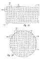
- FIG. 1Ais a top plan view of a rectilinear substrate in accordance with one embodiment of the invention.
- FIG. 1Bis a top plan view of a circular substrate in accordance with another embodiment of the invention.
- FIGS. 2-6illustrate various stages in a method of packaging microelectronic devices in accordance with one embodiment of the invention.
- FIG. 2is a schematic side cross-sectional view of microelectronic devices after microelectronic dies are received in recesses in the substrate.
- FIG. 3is a schematic side cross-sectional view of the microelectronic devices after depositing a dielectric layer and forming vias in the dielectric layer.
- FIG. 4is a schematic side cross-sectional view of the microelectronic devices after forming conductive links.
- FIG. 5is a schematic side cross-sectional view of the microelectronic devices after depositing a second dielectric layer and forming vias in the second dielectric layer.
- FIG. 6is a schematic side cross-sectional view of the microelectronic devices after depositing ball-pads and solder balls.
- FIGS. 7-11illustrate various stages in a method of packaging microelectronic devices in accordance with another embodiment of the invention.
- FIG. 8is a schematic side cross-sectional view of the microelectronic devices after covering the substrate and the microelectronic dies with a first dielectric layer.
- FIG. 9is a schematic side cross-sectional view of the microelectronic devices after forming conductive links.
- FIG. 10is a schematic side cross-sectional view of the microelectronic devices after depositing a second dielectric layer.
- FIG. 11is a schematic side cross-sectional view of the microelectronic devices after depositing ball-pads and solder balls.
- FIG. 1Ais a top plan view of a rectilinear substrate 110 a in accordance with one embodiment of the invention.
- the rectilinear substrate 110 ahas a first surface 111 a with a plurality of recesses 112 .
- the recesses 112can be arranged in a series of columns 116 a and rows 118 a or in another arrangement.
- the recesses 112are shaped to receive one or more microelectronic dies.
- the recesses 112have a generally rectangular shape. In other embodiments, the recesses 112 can have other shapes.
- FIGS. 2-6illustrate various stages in a method of packaging microelectronic devices in accordance with one embodiment of the invention.
- the microelectronic devicesare packaged as part of a batch process.
- a single microelectronic devicecan be packaged according to the illustrated method.
- FIG. 2is a schematic side cross-sectional view of microelectronic devices 100 (identified individually as 100 a - b ) after microelectronic dies are received in recesses in the substrate.
- Each microelectronic device 100can include a portion of a substrate 110 , such as a mounting member, having a recess 112 and a microelectronic die 120 (identified individually as 120 a - b ) received within the recess 112 .
- the substrate 110can be similar to the substrate 110 a described above with reference to FIG. 1A or the substrate 110 b described above with reference to FIG. 1B .
- an adhesive 130is deposited into the recesses 112 of the substrate 110 to bond the microelectronic dies 120 to the substrate 110 .
- the adhesive 130can be deposited into the recesses 112 by placing a volume of adhesive on a first surface 111 of the substrate 110 and moving a wiper blade across the first surface 111 to drive the adhesive 130 into the recesses 112 before placing the dies 120 in the recesses 112 .
- the adhesive 130can be deposited into the recesses 112 by other devices, such as by a pin transfer mechanism or screen-printing.
- the microelectronic devices 100may not include the adhesive 130 .
- the microelectronic dies 120are placed into the recesses 112 of the substrate 110 after singulating the dies 120 .
- the microelectronic dies 120include an integrated circuit 122 (shown schematically), a first side 126 with bond-pads 124 electrically coupled to the integrated circuit 122 , and a second side 128 opposite the first side 126 .
- the microelectronic dies 120are placed into the recesses 112 with the second side 128 facing the substrate 130 .
- the microelectronic dies 120can be placed into the recesses 112 by conventional die attach equipment.
- the recesses 112can have a width D 1 greater than the width D 3 of the microelectronic dies 120 and a depth D 2 greater than the height D 4 of the microelectronic dies 120 . Accordingly, the microelectronic dies 120 are received within the recesses 112 . In other embodiments, the height of the microelectronic die may exceed the depth of the recess.
- each via 150 ais aligned with a corresponding bond-pad 124 .
- the vias 150 acan be formed in the first dielectric layer 140 a by etching, laser drilling, or other suitable processes.
- FIG. 5is a schematic side cross-sectional view of the microelectronic devices 100 after depositing a second dielectric layer and forming vias in the second dielectric layer.
- a second dielectric layer 140 b having a thickness T 2is deposited across the substrate 110 .
- the second dielectric layer 140 bcovers the first dielectric layer 140 a and the conductive links 160 .
- portions of the layer 140 bare removed to create vias 150 b that extend to the conductive links 160 .
- the vias 150 bcan be formed proximate to the ends 161 of the conductive links 160 .
- FIG. 6is a schematic side cross-sectional view of the microelectronic devices 100 after depositing ball-pads and solder balls.
- the vias 150 bare formed in the second dielectric layer 140 b
- ball-pads 170are formed in the vias 150 b and then solder balls 180 are deposited onto the ball-pads 170 .
- the solder balls 180are electrically coupled to the bond-pads 124 of the microelectronic die 120 , and thus the solder balls 180 , ball-pads 170 , and conductive links 160 form a redistribution assembly.
- the solder balls 180are superimposed over the substrate 110 but not the recesses 112 .
- the conductive linksmay have a different length, and accordingly the ball-pads and solder balls can be arranged differently, such as being superimposed over the microelectronic die 120 .
- the substrate 110can be back ground to reduce the profile of the packaged microelectronic devices 100 , and the substrate 110 and dielectric layers 140 a - b can be cut along lines A 1 and A 2 to singulate the microelectronic devices 100 .
- Each microelectronic device 100can be attached to a printed circuit board or other device.
- a microelectronic devicecan include two or more microelectronic dies to create a higher density microelectronic device.
- the substrate 110can be thermally conductive to transfer heat from the microelectronic die 120 to an external heat sink (not shown).
- the substrate 110can comprise copper, aluminum, or an alloy (e.g., an NiFe alloy such as alloy 42 ).
- a substratecan have a coefficient of thermal expansion at least generally similar to the coefficient of thermal expansion of the microelectronic die.
- the thermal stress between the microelectronic die and the substrate caused by thermal cyclingis reduced because the coefficients of thermal expansion of the substrate and the microelectronic die are similar.
- the substratecan have a coefficient of thermal expansion at least generally similar to the coefficient of thermal expansion of a printed circuit board. In these embodiments, the thermal stress between the printed circuitboard and substrate is reduced.
- FIGS. 7-11illustrate various stages in a method of packaging microelectronic devices in accordance with another embodiment of the invention.
- FIG. 7is a schematic side cross-sectional view of microelectronic devices 200 after the microelectronic dies 120 are received in recesses in the substrate 110 and electrical couplers 264 are formed on the dies 120 .
- the microelectronic devices 200are generally similar to the microelectronic devices 100 described above with reference to FIG. 2 .
- the microelectronic devices 200include a substrate 110 having recesses 112 and microelectronic dies 120 received within the recesses 112 .
- the microelectronic devices 200also include a plurality of electrical couplers 264 deposited on the bond-pads 124 of the microelectronic dies 120 . More specifically, the electrical couplers 264 are deposited on a surface 125 of corresponding bond-pads 124 . Accordingly, the electrical couplers 264 can be electrically coupled to the integrated circuit 122 of the microelectronic die 120 .
- FIG. 9is a schematic side cross-sectional view of the microelectronic devices 200 after forming conductive links 260 .
- the conductive links 260are formed on the first surface 241 of the first dielectric layer 240 a to be in physical contact with corresponding electrical couplers 264 .
- the conductive links 260have a first end 262 positioned at least proximate to the top surface 266 of the electrical couplers 264 .
- FIG. 10is a schematic side cross-sectional view of the microelectronic devices 200 after depositing a second dielectric layer 240 b .
- the second dielectric layer 240 bis deposited over the first dielectric layer 240 a and the conductive links 260 .
- portions of the layer 240 bare removed to create vias 250 .
- the vias 250are formed proximate to a second end 261 of the conductive links 260 .
- the vias 250can be formed at other positions along the conductive link 260 .
- FIG. 11is a schematic side cross-sectional view of the microelectronic devices 200 after depositing ball-pads 170 and solder balls 180 .
- a plurality of ball-pads 170are formed in the vias 250 .
- a plurality of solder balls 180are deposited onto corresponding ball-pads 170 .
- the substrate 110 and the dielectric layers 240 a - bcan be cut along lines A 3 and A 4 to singulate the microelectronic devices 200 .
Landscapes
- Engineering & Computer Science (AREA)
- Computer Hardware Design (AREA)
- Microelectronics & Electronic Packaging (AREA)
- Power Engineering (AREA)
- Physics & Mathematics (AREA)
- Condensed Matter Physics & Semiconductors (AREA)
- General Physics & Mathematics (AREA)
- Manufacturing & Machinery (AREA)
- Structures For Mounting Electric Components On Printed Circuit Boards (AREA)
- Production Of Multi-Layered Print Wiring Board (AREA)
- Cooling Or The Like Of Semiconductors Or Solid State Devices (AREA)
Abstract
Description
Claims (23)
Priority Applications (2)
| Application Number | Priority Date | Filing Date | Title |
|---|---|---|---|
| US11/248,384US7329949B2 (en) | 2003-04-22 | 2005-10-11 | Packaged microelectronic devices and methods for packaging microelectronic devices |
| US12/028,211US7655500B2 (en) | 2003-04-22 | 2008-02-08 | Packaged microelectronic devices and methods for packaging microelectronic devices |
Applications Claiming Priority (2)
| Application Number | Priority Date | Filing Date | Title |
|---|---|---|---|
| US10/421,452US7312101B2 (en) | 2003-04-22 | 2003-04-22 | Packaged microelectronic devices and methods for packaging microelectronic devices |
| US11/248,384US7329949B2 (en) | 2003-04-22 | 2005-10-11 | Packaged microelectronic devices and methods for packaging microelectronic devices |
Related Parent Applications (1)
| Application Number | Title | Priority Date | Filing Date |
|---|---|---|---|
| US10/421,452DivisionUS7312101B2 (en) | 2003-04-22 | 2003-04-22 | Packaged microelectronic devices and methods for packaging microelectronic devices |
Related Child Applications (1)
| Application Number | Title | Priority Date | Filing Date |
|---|---|---|---|
| US12/028,211ContinuationUS7655500B2 (en) | 2003-04-22 | 2008-02-08 | Packaged microelectronic devices and methods for packaging microelectronic devices |
Publications (2)
| Publication Number | Publication Date |
|---|---|
| US20060030150A1 US20060030150A1 (en) | 2006-02-09 |
| US7329949B2true US7329949B2 (en) | 2008-02-12 |
Family
ID=33298687
Family Applications (4)
| Application Number | Title | Priority Date | Filing Date |
|---|---|---|---|
| US10/421,452Expired - LifetimeUS7312101B2 (en) | 2003-04-22 | 2003-04-22 | Packaged microelectronic devices and methods for packaging microelectronic devices |
| US11/248,384Expired - LifetimeUS7329949B2 (en) | 2003-04-22 | 2005-10-11 | Packaged microelectronic devices and methods for packaging microelectronic devices |
| US11/964,594Expired - LifetimeUS7550847B2 (en) | 2003-04-22 | 2007-12-26 | Packaged microelectronic devices and methods for packaging microelectronic devices |
| US12/028,211Expired - LifetimeUS7655500B2 (en) | 2003-04-22 | 2008-02-08 | Packaged microelectronic devices and methods for packaging microelectronic devices |
Family Applications Before (1)
| Application Number | Title | Priority Date | Filing Date |
|---|---|---|---|
| US10/421,452Expired - LifetimeUS7312101B2 (en) | 2003-04-22 | 2003-04-22 | Packaged microelectronic devices and methods for packaging microelectronic devices |
Family Applications After (2)
| Application Number | Title | Priority Date | Filing Date |
|---|---|---|---|
| US11/964,594Expired - LifetimeUS7550847B2 (en) | 2003-04-22 | 2007-12-26 | Packaged microelectronic devices and methods for packaging microelectronic devices |
| US12/028,211Expired - LifetimeUS7655500B2 (en) | 2003-04-22 | 2008-02-08 | Packaged microelectronic devices and methods for packaging microelectronic devices |
Country Status (1)
| Country | Link |
|---|---|
| US (4) | US7312101B2 (en) |
Cited By (5)
| Publication number | Priority date | Publication date | Assignee | Title |
|---|---|---|---|---|
| US20080111229A1 (en)* | 2006-11-14 | 2008-05-15 | Samsung Electronics Co., Ltd. | Semiconductor package and method for manufacturing the same |
| US20080132006A1 (en)* | 2003-04-22 | 2008-06-05 | Micron Technology, Inc. | Packaged microelectronic devices and methods for packaging microelectronic devices |
| US20080150164A1 (en)* | 2006-12-20 | 2008-06-26 | Phoenix Precision Technology Corporation | Carrier structure embedded with semiconductor chips and method for manufacturing the same |
| US10381322B1 (en) | 2018-04-23 | 2019-08-13 | Sandisk Technologies Llc | Three-dimensional memory device containing self-aligned interlocking bonded structure and method of making the same |
| US10879260B2 (en) | 2019-02-28 | 2020-12-29 | Sandisk Technologies Llc | Bonded assembly of a support die and plural memory dies containing laterally shifted vertical interconnections and methods for making the same |
Families Citing this family (75)
| Publication number | Priority date | Publication date | Assignee | Title |
|---|---|---|---|---|
| TWI246761B (en)* | 2003-05-14 | 2006-01-01 | Siliconware Precision Industries Co Ltd | Semiconductor package with build-up layers formed on chip and fabrication method of the semiconductor package |
| US6934065B2 (en)* | 2003-09-18 | 2005-08-23 | Micron Technology, Inc. | Microelectronic devices and methods for packaging microelectronic devices |
| US7583862B2 (en)* | 2003-11-26 | 2009-09-01 | Aptina Imaging Corporation | Packaged microelectronic imagers and methods of packaging microelectronic imagers |
| US7253397B2 (en)* | 2004-02-23 | 2007-08-07 | Micron Technology, Inc. | Packaged microelectronic imagers and methods of packaging microelectronic imagers |
| US8092734B2 (en) | 2004-05-13 | 2012-01-10 | Aptina Imaging Corporation | Covers for microelectronic imagers and methods for wafer-level packaging of microelectronics imagers |
| US7253957B2 (en)* | 2004-05-13 | 2007-08-07 | Micron Technology, Inc. | Integrated optics units and methods of manufacturing integrated optics units for use with microelectronic imagers |
| US20050275750A1 (en) | 2004-06-09 | 2005-12-15 | Salman Akram | Wafer-level packaged microelectronic imagers and processes for wafer-level packaging |
| US7498647B2 (en) | 2004-06-10 | 2009-03-03 | Micron Technology, Inc. | Packaged microelectronic imagers and methods of packaging microelectronic imagers |
| US7199439B2 (en)* | 2004-06-14 | 2007-04-03 | Micron Technology, Inc. | Microelectronic imagers and methods of packaging microelectronic imagers |
| US7262405B2 (en)* | 2004-06-14 | 2007-08-28 | Micron Technology, Inc. | Prefabricated housings for microelectronic imagers |
| US7232754B2 (en) | 2004-06-29 | 2007-06-19 | Micron Technology, Inc. | Microelectronic devices and methods for forming interconnects in microelectronic devices |
| US7294897B2 (en)* | 2004-06-29 | 2007-11-13 | Micron Technology, Inc. | Packaged microelectronic imagers and methods of packaging microelectronic imagers |
| US7416913B2 (en)* | 2004-07-16 | 2008-08-26 | Micron Technology, Inc. | Methods of manufacturing microelectronic imaging units with discrete standoffs |
| US7189954B2 (en)* | 2004-07-19 | 2007-03-13 | Micron Technology, Inc. | Microelectronic imagers with optical devices and methods of manufacturing such microelectronic imagers |
| US7402453B2 (en)* | 2004-07-28 | 2008-07-22 | Micron Technology, Inc. | Microelectronic imaging units and methods of manufacturing microelectronic imaging units |
| US7364934B2 (en)* | 2004-08-10 | 2008-04-29 | Micron Technology, Inc. | Microelectronic imaging units and methods of manufacturing microelectronic imaging units |
| US7397066B2 (en)* | 2004-08-19 | 2008-07-08 | Micron Technology, Inc. | Microelectronic imagers with curved image sensors and methods for manufacturing microelectronic imagers |
| US7223626B2 (en)* | 2004-08-19 | 2007-05-29 | Micron Technology, Inc. | Spacers for packaged microelectronic imagers and methods of making and using spacers for wafer-level packaging of imagers |
| US7429494B2 (en)* | 2004-08-24 | 2008-09-30 | Micron Technology, Inc. | Microelectronic imagers with optical devices having integral reference features and methods for manufacturing such microelectronic imagers |
| US7115961B2 (en)* | 2004-08-24 | 2006-10-03 | Micron Technology, Inc. | Packaged microelectronic imaging devices and methods of packaging microelectronic imaging devices |
| US7425499B2 (en) | 2004-08-24 | 2008-09-16 | Micron Technology, Inc. | Methods for forming interconnects in vias and microelectronic workpieces including such interconnects |
| US7276393B2 (en)* | 2004-08-26 | 2007-10-02 | Micron Technology, Inc. | Microelectronic imaging units and methods of manufacturing microelectronic imaging units |
| US20070148807A1 (en)* | 2005-08-22 | 2007-06-28 | Salman Akram | Microelectronic imagers with integrated optical devices and methods for manufacturing such microelectronic imagers |
| US7511262B2 (en)* | 2004-08-30 | 2009-03-31 | Micron Technology, Inc. | Optical device and assembly for use with imaging dies, and wafer-label imager assembly |
| US7646075B2 (en)* | 2004-08-31 | 2010-01-12 | Micron Technology, Inc. | Microelectronic imagers having front side contacts |
| US7300857B2 (en) | 2004-09-02 | 2007-11-27 | Micron Technology, Inc. | Through-wafer interconnects for photoimager and memory wafers |
| KR100577430B1 (en) | 2004-09-03 | 2006-05-08 | 삼성전자주식회사 | Display device |
| US20070129402A1 (en)* | 2004-12-27 | 2007-06-07 | Eisai Research Institute | Sustained release formulations |
| US20060141666A1 (en)* | 2004-12-29 | 2006-06-29 | Infineon Technologies Ag | Method for producing a module including an integrated circuit on a substrate and an integrated module manufactured thereby |
| US7271482B2 (en) | 2004-12-30 | 2007-09-18 | Micron Technology, Inc. | Methods for forming interconnects in microelectronic workpieces and microelectronic workpieces formed using such methods |
| US7214919B2 (en)* | 2005-02-08 | 2007-05-08 | Micron Technology, Inc. | Microelectronic imaging units and methods of manufacturing microelectronic imaging units |
| US7303931B2 (en)* | 2005-02-10 | 2007-12-04 | Micron Technology, Inc. | Microfeature workpieces having microlenses and methods of forming microlenses on microfeature workpieces |
| US20060177999A1 (en)* | 2005-02-10 | 2006-08-10 | Micron Technology, Inc. | Microelectronic workpieces and methods for forming interconnects in microelectronic workpieces |
| US7190039B2 (en)* | 2005-02-18 | 2007-03-13 | Micron Technology, Inc. | Microelectronic imagers with shaped image sensors and methods for manufacturing microelectronic imagers |
| DE102005008600B9 (en)* | 2005-02-23 | 2012-06-21 | Infineon Technologies Ag | Chip carrier, chip carrier system and semiconductor chips, and method of making a chip carrier and system |
| US7212699B2 (en)* | 2005-03-25 | 2007-05-01 | Hewlett-Packard Development Company, L.P. | Fabricating a photonic die |
| US7795134B2 (en)* | 2005-06-28 | 2010-09-14 | Micron Technology, Inc. | Conductive interconnect structures and formation methods using supercritical fluids |
| US7170159B1 (en)* | 2005-07-07 | 2007-01-30 | Taiwan Semiconductor Manufacturing Company, Ltd. | Low CTE substrates for use with low-k flip-chip package devices |
| US7807505B2 (en) | 2005-08-30 | 2010-10-05 | Micron Technology, Inc. | Methods for wafer-level packaging of microfeature devices and microfeature devices formed using such methods |
| US7745944B2 (en) | 2005-08-31 | 2010-06-29 | Micron Technology, Inc. | Microelectronic devices having intermediate contacts for connection to interposer substrates, and associated methods of packaging microelectronic devices with intermediate contacts |
| US7288757B2 (en) | 2005-09-01 | 2007-10-30 | Micron Technology, Inc. | Microelectronic imaging devices and associated methods for attaching transmissive elements |
| US7622377B2 (en) | 2005-09-01 | 2009-11-24 | Micron Technology, Inc. | Microfeature workpiece substrates having through-substrate vias, and associated methods of formation |
| US7262134B2 (en)* | 2005-09-01 | 2007-08-28 | Micron Technology, Inc. | Microfeature workpieces and methods for forming interconnects in microfeature workpieces |
| TW200731477A (en)* | 2005-11-10 | 2007-08-16 | Int Rectifier Corp | Semiconductor package including a semiconductor die having redistributed pads |
| US20070138628A1 (en)* | 2005-12-15 | 2007-06-21 | Lam Ken M | Apparatus and method for increasing the quantity of discrete electronic components in an integrated circuit package |
| SG135074A1 (en)* | 2006-02-28 | 2007-09-28 | Micron Technology Inc | Microelectronic devices, stacked microelectronic devices, and methods for manufacturing such devices |
| US8021981B2 (en)* | 2006-08-30 | 2011-09-20 | Micron Technology, Inc. | Redistribution layers for microfeature workpieces, and associated systems and methods |
| US7830004B2 (en)* | 2006-10-27 | 2010-11-09 | Taiwan Semiconductor Manufacturing Company, Ltd. | Packaging with base layers comprising alloy 42 |
| US8049323B2 (en)* | 2007-02-16 | 2011-11-01 | Taiwan Semiconductor Manufacturing Co., Ltd. | Chip holder with wafer level redistribution layer |
| JP2008211125A (en) | 2007-02-28 | 2008-09-11 | Spansion Llc | Semiconductor device and its manufacturing method |
| JP2008227232A (en)* | 2007-03-14 | 2008-09-25 | Matsushita Electric Ind Co Ltd | Semiconductor device manufacturing method, semiconductor device, and optical pickup module |
| GB2451921A (en)* | 2007-08-17 | 2009-02-18 | Wolfson Microelectronics Plc | MEMS package |
| GB2451908B (en)* | 2007-08-17 | 2009-12-02 | Wolfson Microelectronics Plc | Mems package |
| US7772691B2 (en)* | 2007-10-12 | 2010-08-10 | Taiwan Semiconductor Manufacturing Company, Ltd. | Thermally enhanced wafer level package |
| US20090261469A1 (en)* | 2008-04-21 | 2009-10-22 | Qwan Ho Chung | Semiconductor package and method for manufacturing the same |
| KR100992778B1 (en)* | 2008-05-23 | 2010-11-05 | 엘지이노텍 주식회사 | Light emitting device package and method for manufacturing the same |
| US7863096B2 (en)* | 2008-07-17 | 2011-01-04 | Fairchild Semiconductor Corporation | Embedded die package and process flow using a pre-molded carrier |
| US8030780B2 (en) | 2008-10-16 | 2011-10-04 | Micron Technology, Inc. | Semiconductor substrates with unitary vias and via terminals, and associated systems and methods |
| US8119454B2 (en)* | 2008-12-08 | 2012-02-21 | Stmicroelectronics Asia Pacific Pte Ltd. | Manufacturing fan-out wafer level packaging |
| US20100148357A1 (en)* | 2008-12-16 | 2010-06-17 | Freescale Semiconductor, Inc. | Method of packaging integrated circuit dies with thermal dissipation capability |
| US20100194465A1 (en)* | 2009-02-02 | 2010-08-05 | Ali Salih | Temperature compensated current source and method therefor |
| WO2010106473A1 (en)* | 2009-03-16 | 2010-09-23 | Nxp B.V. | Packaged semiconductor product and method for manufacture thereof |
| US8148206B2 (en)* | 2009-10-27 | 2012-04-03 | Freescale Semiconductor, Inc. | Package for high power integrated circuits and method for forming |
| US8237278B2 (en)* | 2009-11-16 | 2012-08-07 | International Business Machines Corporation | Configurable interposer |
| US8138014B2 (en)* | 2010-01-29 | 2012-03-20 | Stats Chippac, Ltd. | Method of forming thin profile WLCSP with vertical interconnect over package footprint |
| US20110215450A1 (en)* | 2010-03-05 | 2011-09-08 | Chi Heejo | Integrated circuit packaging system with encapsulation and method of manufacture thereof |
| US8076181B1 (en)* | 2010-10-22 | 2011-12-13 | Linear Technology Corporation | Lead plating technique for singulated IC packages |
| TWI446501B (en)* | 2012-01-20 | 2014-07-21 | 矽品精密工業股份有限公司 | Carrier board, semiconductor package and method of forming same |
| US8772058B2 (en)* | 2012-02-02 | 2014-07-08 | Harris Corporation | Method for making a redistributed wafer using transferrable redistribution layers |
| US8846452B2 (en)* | 2012-08-21 | 2014-09-30 | Infineon Technologies Ag | Semiconductor device package and methods of packaging thereof |
| US9056763B2 (en)* | 2013-09-27 | 2015-06-16 | Intel Corporation | Stress buffer layer for integrated microelectromechanical systems (MEMS) |
| US20150380369A1 (en)* | 2013-09-30 | 2015-12-31 | Nantong Fujitsu Microelectronics Co., Ltd | Wafer packaging structure and packaging method |
| US9299651B2 (en)* | 2013-11-20 | 2016-03-29 | Bridge Semiconductor Corporation | Semiconductor assembly and method of manufacturing the same |
| TWI548049B (en)* | 2014-09-19 | 2016-09-01 | 矽品精密工業股份有限公司 | Semiconductor structure and method of manufacture |
| CN111341750B (en)* | 2018-12-19 | 2024-03-01 | 奥特斯奥地利科技与系统技术有限公司 | Component carrier comprising an electrically conductive base structure and method of manufacture |
Citations (26)
| Publication number | Priority date | Publication date | Assignee | Title |
|---|---|---|---|---|
| US4931853A (en) | 1986-05-20 | 1990-06-05 | Kabushiki Kaisha Toshiba | IC card and method of manufacturing the same |
| US5008213A (en) | 1988-12-09 | 1991-04-16 | The United States Of America As Represented By The Secretary Of The Air Force | Hybrid wafer scale microcircuit integration |
| US5081563A (en) | 1990-04-27 | 1992-01-14 | International Business Machines Corporation | Multi-layer package incorporating a recessed cavity for a semiconductor chip |
| US5409865A (en)* | 1993-09-03 | 1995-04-25 | Advanced Semiconductor Assembly Technology | Process for assembling a TAB grid array package for an integrated circuit |
| US5851845A (en) | 1995-12-18 | 1998-12-22 | Micron Technology, Inc. | Process for packaging a semiconductor die using dicing and testing |
| US5933713A (en) | 1998-04-06 | 1999-08-03 | Micron Technology, Inc. | Method of forming overmolded chip scale package and resulting product |
| US5946553A (en) | 1991-06-04 | 1999-08-31 | Micron Technology, Inc. | Process for manufacturing a semiconductor package with bi-substrate die |
| US6004867A (en) | 1996-12-16 | 1999-12-21 | Samsung Electronics Co., Ltd. | Chip-size packages assembled using mass production techniques at the wafer-level |
| US6008070A (en) | 1998-05-21 | 1999-12-28 | Micron Technology, Inc. | Wafer level fabrication and assembly of chip scale packages |
| US6072236A (en) | 1996-03-07 | 2000-06-06 | Micron Technology, Inc. | Micromachined chip scale package |
| US6184465B1 (en) | 1998-11-12 | 2001-02-06 | Micron Technology, Inc. | Semiconductor package |
| US6187615B1 (en) | 1998-08-28 | 2001-02-13 | Samsung Electronics Co., Ltd. | Chip scale packages and methods for manufacturing the chip scale packages at wafer level |
| US6225695B1 (en)* | 1997-06-05 | 2001-05-01 | Lsi Logic Corporation | Grooved semiconductor die for flip-chip heat sink attachment |
| US6228687B1 (en) | 1999-06-28 | 2001-05-08 | Micron Technology, Inc. | Wafer-level package and methods of fabricating |
| US6235552B1 (en) | 1999-07-09 | 2001-05-22 | Samsung Electronics Co., Ltd. | Chip scale package and method for manufacturing the same using a redistribution substrate |
| US6271469B1 (en) | 1999-11-12 | 2001-08-07 | Intel Corporation | Direct build-up layer on an encapsulated die package |
| US6326698B1 (en) | 2000-06-08 | 2001-12-04 | Micron Technology, Inc. | Semiconductor devices having protective layers thereon through which contact pads are exposed and stereolithographic methods of fabricating such semiconductor devices |
| US6407381B1 (en) | 2000-07-05 | 2002-06-18 | Amkor Technology, Inc. | Wafer scale image sensor package |
| US6452255B1 (en)* | 2000-03-20 | 2002-09-17 | National Semiconductor, Corp. | Low inductance leadless package |
| US6459163B1 (en) | 2001-03-21 | 2002-10-01 | United Test Center, Inc. | Semiconductor device and method for fabricating the same |
| US6503780B1 (en) | 2000-07-05 | 2003-01-07 | Amkor Technology, Inc. | Wafer scale image sensor package fabrication method |
| US6537848B2 (en) | 2001-05-30 | 2003-03-25 | St. Assembly Test Services Ltd. | Super thin/super thermal ball grid array package |
| US6709898B1 (en) | 2000-10-04 | 2004-03-23 | Intel Corporation | Die-in-heat spreader microelectronic package |
| US20040135269A1 (en)* | 2002-07-23 | 2004-07-15 | Seiko Epson Corporation | Interconnect substrate, semiconductor device, methods of manufacturing the same, circuit board, and electronic equipment |
| US20040150101A1 (en) | 2003-01-30 | 2004-08-05 | Endicott Interconnect Technologies, Inc. | Information handling system |
| US20040214373A1 (en) | 2003-04-22 | 2004-10-28 | Tongbi Jiang | Packaged microelectronic devices and methods for packaging microelectronic devices |
Family Cites Families (12)
| Publication number | Priority date | Publication date | Assignee | Title |
|---|---|---|---|---|
| FR2618617B1 (en) | 1987-07-23 | 1989-11-17 | Merlin Gerin | DEVICE FOR FILTERING COMMON MODE DISTURBANCES AFFECTING THE CARDS OF A STATIC POWER CONVERTER |
| US5000821A (en) | 1988-05-25 | 1991-03-19 | Resources Conservation Company | Apparatus for controlling solid particle flow in an evaporator |
| US5400986A (en) | 1993-02-08 | 1995-03-28 | Martin Marietta Corporation | Optical solar reflector and mounting method |
| JPH08274906A (en) | 1995-03-31 | 1996-10-18 | Canon Inc | Output device and image processing method |
| IT1277204B1 (en) | 1995-10-19 | 1997-11-05 | Pirelli S P A Ora Pirelli Cavi | TRANSPARENT OPTICAL COMMUNICATION NETWORK WITH SELF-PROTECTED RING |
| US5904655A (en) | 1996-06-27 | 1999-05-18 | Brackett; Jacqueline D. | Disposable blood pressure cover and method for utilizing the same |
| DE69829895T2 (en) | 1997-01-17 | 2006-03-09 | Stanley Electric Co. Ltd. | headlights |
| US6000486A (en) | 1997-04-18 | 1999-12-14 | Medicart, L.L.C. | Apparatus for providing self-propelled motion to medication carts |
| US5833350A (en) | 1997-04-25 | 1998-11-10 | Electro Static Solutions, Llc | Switch cover plate providing automatic emergency lighting |
| ES2170990T3 (en) | 1997-12-10 | 2002-08-16 | Lonza Ag | PROCEDURE FOR THE PREPARATION OF ETINYL-CYCLOPROPANE. |
| US6102463A (en) | 1999-05-18 | 2000-08-15 | Delphi Technologies, Inc. | Vehicle seat assembly with hidden storage compartment |
| US20030059976A1 (en)* | 2001-09-24 | 2003-03-27 | Nathan Richard J. | Integrated package and methods for making same |
- 2003
- 2003-04-22USUS10/421,452patent/US7312101B2/ennot_activeExpired - Lifetime
- 2005
- 2005-10-11USUS11/248,384patent/US7329949B2/ennot_activeExpired - Lifetime
- 2007
- 2007-12-26USUS11/964,594patent/US7550847B2/ennot_activeExpired - Lifetime
- 2008
- 2008-02-08USUS12/028,211patent/US7655500B2/ennot_activeExpired - Lifetime
Patent Citations (29)
| Publication number | Priority date | Publication date | Assignee | Title |
|---|---|---|---|---|
| US4931853A (en) | 1986-05-20 | 1990-06-05 | Kabushiki Kaisha Toshiba | IC card and method of manufacturing the same |
| US5008213A (en) | 1988-12-09 | 1991-04-16 | The United States Of America As Represented By The Secretary Of The Air Force | Hybrid wafer scale microcircuit integration |
| US5081563A (en) | 1990-04-27 | 1992-01-14 | International Business Machines Corporation | Multi-layer package incorporating a recessed cavity for a semiconductor chip |
| US5946553A (en) | 1991-06-04 | 1999-08-31 | Micron Technology, Inc. | Process for manufacturing a semiconductor package with bi-substrate die |
| US6020624A (en) | 1991-06-04 | 2000-02-01 | Micron Technology, Inc. | Semiconductor package with bi-substrate die |
| US5409865A (en)* | 1993-09-03 | 1995-04-25 | Advanced Semiconductor Assembly Technology | Process for assembling a TAB grid array package for an integrated circuit |
| US5851845A (en) | 1995-12-18 | 1998-12-22 | Micron Technology, Inc. | Process for packaging a semiconductor die using dicing and testing |
| US6072236A (en) | 1996-03-07 | 2000-06-06 | Micron Technology, Inc. | Micromachined chip scale package |
| US6124634A (en) | 1996-03-07 | 2000-09-26 | Micron Technology, Inc. | Micromachined chip scale package |
| US6004867A (en) | 1996-12-16 | 1999-12-21 | Samsung Electronics Co., Ltd. | Chip-size packages assembled using mass production techniques at the wafer-level |
| US6225695B1 (en)* | 1997-06-05 | 2001-05-01 | Lsi Logic Corporation | Grooved semiconductor die for flip-chip heat sink attachment |
| US5933713A (en) | 1998-04-06 | 1999-08-03 | Micron Technology, Inc. | Method of forming overmolded chip scale package and resulting product |
| US6326697B1 (en) | 1998-05-21 | 2001-12-04 | Micron Technology, Inc. | Hermetically sealed chip scale packages formed by wafer level fabrication and assembly |
| US6008070A (en) | 1998-05-21 | 1999-12-28 | Micron Technology, Inc. | Wafer level fabrication and assembly of chip scale packages |
| US6187615B1 (en) | 1998-08-28 | 2001-02-13 | Samsung Electronics Co., Ltd. | Chip scale packages and methods for manufacturing the chip scale packages at wafer level |
| US6184465B1 (en) | 1998-11-12 | 2001-02-06 | Micron Technology, Inc. | Semiconductor package |
| US6228687B1 (en) | 1999-06-28 | 2001-05-08 | Micron Technology, Inc. | Wafer-level package and methods of fabricating |
| US6235552B1 (en) | 1999-07-09 | 2001-05-22 | Samsung Electronics Co., Ltd. | Chip scale package and method for manufacturing the same using a redistribution substrate |
| US6271469B1 (en) | 1999-11-12 | 2001-08-07 | Intel Corporation | Direct build-up layer on an encapsulated die package |
| US6452255B1 (en)* | 2000-03-20 | 2002-09-17 | National Semiconductor, Corp. | Low inductance leadless package |
| US6326698B1 (en) | 2000-06-08 | 2001-12-04 | Micron Technology, Inc. | Semiconductor devices having protective layers thereon through which contact pads are exposed and stereolithographic methods of fabricating such semiconductor devices |
| US6407381B1 (en) | 2000-07-05 | 2002-06-18 | Amkor Technology, Inc. | Wafer scale image sensor package |
| US6503780B1 (en) | 2000-07-05 | 2003-01-07 | Amkor Technology, Inc. | Wafer scale image sensor package fabrication method |
| US6709898B1 (en) | 2000-10-04 | 2004-03-23 | Intel Corporation | Die-in-heat spreader microelectronic package |
| US6459163B1 (en) | 2001-03-21 | 2002-10-01 | United Test Center, Inc. | Semiconductor device and method for fabricating the same |
| US6537848B2 (en) | 2001-05-30 | 2003-03-25 | St. Assembly Test Services Ltd. | Super thin/super thermal ball grid array package |
| US20040135269A1 (en)* | 2002-07-23 | 2004-07-15 | Seiko Epson Corporation | Interconnect substrate, semiconductor device, methods of manufacturing the same, circuit board, and electronic equipment |
| US20040150101A1 (en) | 2003-01-30 | 2004-08-05 | Endicott Interconnect Technologies, Inc. | Information handling system |
| US20040214373A1 (en) | 2003-04-22 | 2004-10-28 | Tongbi Jiang | Packaged microelectronic devices and methods for packaging microelectronic devices |
Cited By (9)
| Publication number | Priority date | Publication date | Assignee | Title |
|---|---|---|---|---|
| US20080132006A1 (en)* | 2003-04-22 | 2008-06-05 | Micron Technology, Inc. | Packaged microelectronic devices and methods for packaging microelectronic devices |
| US7655500B2 (en) | 2003-04-22 | 2010-02-02 | Micron Technology | Packaged microelectronic devices and methods for packaging microelectronic devices |
| US20080111229A1 (en)* | 2006-11-14 | 2008-05-15 | Samsung Electronics Co., Ltd. | Semiconductor package and method for manufacturing the same |
| US7649250B2 (en)* | 2006-11-14 | 2010-01-19 | Samsung Electronics Co., Ltd. | Semiconductor package |
| US20100136747A1 (en)* | 2006-11-14 | 2010-06-03 | Samsung Electronics Co., Ltd. | Method for manufacturing semiconductor package |
| US20080150164A1 (en)* | 2006-12-20 | 2008-06-26 | Phoenix Precision Technology Corporation | Carrier structure embedded with semiconductor chips and method for manufacturing the same |
| US7829987B2 (en)* | 2006-12-20 | 2010-11-09 | Unimicron Technology Corp. | Carrier structure embedded with semiconductor chips and method for manufacturing the same |
| US10381322B1 (en) | 2018-04-23 | 2019-08-13 | Sandisk Technologies Llc | Three-dimensional memory device containing self-aligned interlocking bonded structure and method of making the same |
| US10879260B2 (en) | 2019-02-28 | 2020-12-29 | Sandisk Technologies Llc | Bonded assembly of a support die and plural memory dies containing laterally shifted vertical interconnections and methods for making the same |
Also Published As
| Publication number | Publication date |
|---|---|
| US20060030150A1 (en) | 2006-02-09 |
| US7550847B2 (en) | 2009-06-23 |
| US20080132006A1 (en) | 2008-06-05 |
| US7655500B2 (en) | 2010-02-02 |
| US20080099917A1 (en) | 2008-05-01 |
| US20040214373A1 (en) | 2004-10-28 |
| US7312101B2 (en) | 2007-12-25 |
Similar Documents
| Publication | Publication Date | Title |
|---|---|---|
| US7329949B2 (en) | Packaged microelectronic devices and methods for packaging microelectronic devices | |
| US7754531B2 (en) | Method for packaging microelectronic devices | |
| US6777788B1 (en) | Method and structure for applying thick solder layer onto die attach pad | |
| US8304896B2 (en) | Embedded die package and process flow using a pre-molded carrier | |
| US7247934B2 (en) | Multi-chip semiconductor package | |
| US9318411B2 (en) | Semiconductor package with package-on-package stacking capability and method of manufacturing the same | |
| US6740961B1 (en) | Lead frame design for chip scale package | |
| TWI573201B (en) | Packaging structural member | |
| US7927918B2 (en) | Packaged products, including stacked package modules, and methods of forming same | |
| US7981796B2 (en) | Methods for forming packaged products | |
| US9230901B2 (en) | Semiconductor device having chip embedded in heat spreader and electrically connected to interposer and method of manufacturing the same | |
| US20070111379A1 (en) | Pre-molded leadframe and method therefor | |
| US7652376B2 (en) | Integrated circuit package system including stacked die | |
| US8124459B2 (en) | Bump chip carrier semiconductor package system | |
| US9899208B2 (en) | Molded leadframe substrate semiconductor package | |
| JP2008166752A (en) | Multichip structure and method for forming the same | |
| US20070093000A1 (en) | Pre-molded leadframe and method therefor | |
| US20060202315A1 (en) | Microelectronic devices having conductive complementary structures and methods of manufacturing microelectronic devices have conductive complementary structures | |
| KR20080114603A (en) | Semiconductor device package with pseudo chip | |
| US6339253B1 (en) | Semiconductor package | |
| US9761435B1 (en) | Flip chip cavity package | |
| US20050194698A1 (en) | Integrated circuit package with keep-out zone overlapping undercut zone | |
| US9947605B2 (en) | Flip chip cavity package | |
| US20250046733A1 (en) | Semiconductor device and process with crack reduction |
Legal Events
| Date | Code | Title | Description |
|---|---|---|---|
| FEPP | Fee payment procedure | Free format text:PAYOR NUMBER ASSIGNED (ORIGINAL EVENT CODE: ASPN); ENTITY STATUS OF PATENT OWNER: LARGE ENTITY | |
| STCF | Information on status: patent grant | Free format text:PATENTED CASE | |
| FPAY | Fee payment | Year of fee payment:4 | |
| FPAY | Fee payment | Year of fee payment:8 | |
| AS | Assignment | Owner name:U.S. BANK NATIONAL ASSOCIATION, AS COLLATERAL AGENT, CALIFORNIA Free format text:SECURITY INTEREST;ASSIGNOR:MICRON TECHNOLOGY, INC.;REEL/FRAME:038669/0001 Effective date:20160426 Owner name:U.S. BANK NATIONAL ASSOCIATION, AS COLLATERAL AGEN Free format text:SECURITY INTEREST;ASSIGNOR:MICRON TECHNOLOGY, INC.;REEL/FRAME:038669/0001 Effective date:20160426 | |
| AS | Assignment | Owner name:MORGAN STANLEY SENIOR FUNDING, INC., AS COLLATERAL AGENT, MARYLAND Free format text:PATENT SECURITY AGREEMENT;ASSIGNOR:MICRON TECHNOLOGY, INC.;REEL/FRAME:038954/0001 Effective date:20160426 Owner name:MORGAN STANLEY SENIOR FUNDING, INC., AS COLLATERAL Free format text:PATENT SECURITY AGREEMENT;ASSIGNOR:MICRON TECHNOLOGY, INC.;REEL/FRAME:038954/0001 Effective date:20160426 | |
| AS | Assignment | Owner name:U.S. BANK NATIONAL ASSOCIATION, AS COLLATERAL AGENT, CALIFORNIA Free format text:CORRECTIVE ASSIGNMENT TO CORRECT THE REPLACE ERRONEOUSLY FILED PATENT #7358718 WITH THE CORRECT PATENT #7358178 PREVIOUSLY RECORDED ON REEL 038669 FRAME 0001. ASSIGNOR(S) HEREBY CONFIRMS THE SECURITY INTEREST;ASSIGNOR:MICRON TECHNOLOGY, INC.;REEL/FRAME:043079/0001 Effective date:20160426 Owner name:U.S. BANK NATIONAL ASSOCIATION, AS COLLATERAL AGEN Free format text:CORRECTIVE ASSIGNMENT TO CORRECT THE REPLACE ERRONEOUSLY FILED PATENT #7358718 WITH THE CORRECT PATENT #7358178 PREVIOUSLY RECORDED ON REEL 038669 FRAME 0001. ASSIGNOR(S) HEREBY CONFIRMS THE SECURITY INTEREST;ASSIGNOR:MICRON TECHNOLOGY, INC.;REEL/FRAME:043079/0001 Effective date:20160426 | |
| AS | Assignment | Owner name:JPMORGAN CHASE BANK, N.A., AS COLLATERAL AGENT, ILLINOIS Free format text:SECURITY INTEREST;ASSIGNORS:MICRON TECHNOLOGY, INC.;MICRON SEMICONDUCTOR PRODUCTS, INC.;REEL/FRAME:047540/0001 Effective date:20180703 Owner name:JPMORGAN CHASE BANK, N.A., AS COLLATERAL AGENT, IL Free format text:SECURITY INTEREST;ASSIGNORS:MICRON TECHNOLOGY, INC.;MICRON SEMICONDUCTOR PRODUCTS, INC.;REEL/FRAME:047540/0001 Effective date:20180703 | |
| AS | Assignment | Owner name:MICRON TECHNOLOGY, INC., IDAHO Free format text:RELEASE BY SECURED PARTY;ASSIGNOR:U.S. BANK NATIONAL ASSOCIATION, AS COLLATERAL AGENT;REEL/FRAME:047243/0001 Effective date:20180629 | |
| MAFP | Maintenance fee payment | Free format text:PAYMENT OF MAINTENANCE FEE, 12TH YEAR, LARGE ENTITY (ORIGINAL EVENT CODE: M1553); ENTITY STATUS OF PATENT OWNER: LARGE ENTITY Year of fee payment:12 | |
| AS | Assignment | Owner name:MICRON TECHNOLOGY, INC., IDAHO Free format text:RELEASE BY SECURED PARTY;ASSIGNOR:MORGAN STANLEY SENIOR FUNDING, INC., AS COLLATERAL AGENT;REEL/FRAME:050937/0001 Effective date:20190731 | |
| AS | Assignment | Owner name:MICRON SEMICONDUCTOR PRODUCTS, INC., IDAHO Free format text:RELEASE BY SECURED PARTY;ASSIGNOR:JPMORGAN CHASE BANK, N.A., AS COLLATERAL AGENT;REEL/FRAME:051028/0001 Effective date:20190731 Owner name:MICRON TECHNOLOGY, INC., IDAHO Free format text:RELEASE BY SECURED PARTY;ASSIGNOR:JPMORGAN CHASE BANK, N.A., AS COLLATERAL AGENT;REEL/FRAME:051028/0001 Effective date:20190731 |