US7329924B2 - Integrated circuits and methods of forming a field effect transistor - Google Patents
Integrated circuits and methods of forming a field effect transistorDownload PDFInfo
- Publication number
- US7329924B2 US7329924B2US11/704,487US70448707AUS7329924B2US 7329924 B2US7329924 B2US 7329924B2US 70448707 AUS70448707 AUS 70448707AUS 7329924 B2US7329924 B2US 7329924B2
- Authority
- US
- United States
- Prior art keywords
- silicon
- source
- drain regions
- field effect
- bulk semiconductive
- Prior art date
- Legal status (The legal status is an assumption and is not a legal conclusion. Google has not performed a legal analysis and makes no representation as to the accuracy of the status listed.)
- Expired - Lifetime
Links
Images


Classifications
- H—ELECTRICITY
- H10—SEMICONDUCTOR DEVICES; ELECTRIC SOLID-STATE DEVICES NOT OTHERWISE PROVIDED FOR
- H10D—INORGANIC ELECTRIC SEMICONDUCTOR DEVICES
- H10D62/00—Semiconductor bodies, or regions thereof, of devices having potential barriers
- H10D62/10—Shapes, relative sizes or dispositions of the regions of the semiconductor bodies; Shapes of the semiconductor bodies
- H10D62/113—Isolations within a component, i.e. internal isolations
- H10D62/115—Dielectric isolations, e.g. air gaps
- H10D62/116—Dielectric isolations, e.g. air gaps adjoining the input or output regions of field-effect devices, e.g. adjoining source or drain regions
- H—ELECTRICITY
- H01—ELECTRIC ELEMENTS
- H01L—SEMICONDUCTOR DEVICES NOT COVERED BY CLASS H10
- H01L21/00—Processes or apparatus adapted for the manufacture or treatment of semiconductor or solid state devices or of parts thereof
- H01L21/02—Manufacture or treatment of semiconductor devices or of parts thereof
- H01L21/02104—Forming layers
- H01L21/02365—Forming inorganic semiconducting materials on a substrate
- H01L21/02367—Substrates
- H01L21/0237—Materials
- H—ELECTRICITY
- H01—ELECTRIC ELEMENTS
- H01L—SEMICONDUCTOR DEVICES NOT COVERED BY CLASS H10
- H01L21/00—Processes or apparatus adapted for the manufacture or treatment of semiconductor or solid state devices or of parts thereof
- H01L21/02—Manufacture or treatment of semiconductor devices or of parts thereof
- H01L21/02104—Forming layers
- H01L21/02365—Forming inorganic semiconducting materials on a substrate
- H01L21/02518—Deposited layers
- H01L21/02521—Materials
- H01L21/02524—Group 14 semiconducting materials
- H01L21/02532—Silicon, silicon germanium, germanium
- H—ELECTRICITY
- H01—ELECTRIC ELEMENTS
- H01L—SEMICONDUCTOR DEVICES NOT COVERED BY CLASS H10
- H01L21/00—Processes or apparatus adapted for the manufacture or treatment of semiconductor or solid state devices or of parts thereof
- H01L21/02—Manufacture or treatment of semiconductor devices or of parts thereof
- H01L21/02104—Forming layers
- H01L21/02365—Forming inorganic semiconducting materials on a substrate
- H01L21/02518—Deposited layers
- H01L21/02587—Structure
- H01L21/0259—Microstructure
- H01L21/02595—Microstructure polycrystalline
- H—ELECTRICITY
- H01—ELECTRIC ELEMENTS
- H01L—SEMICONDUCTOR DEVICES NOT COVERED BY CLASS H10
- H01L21/00—Processes or apparatus adapted for the manufacture or treatment of semiconductor or solid state devices or of parts thereof
- H01L21/02—Manufacture or treatment of semiconductor devices or of parts thereof
- H01L21/02104—Forming layers
- H01L21/02365—Forming inorganic semiconducting materials on a substrate
- H01L21/02612—Formation types
- H01L21/02617—Deposition types
- H01L21/0262—Reduction or decomposition of gaseous compounds, e.g. CVD
- H—ELECTRICITY
- H10—SEMICONDUCTOR DEVICES; ELECTRIC SOLID-STATE DEVICES NOT OTHERWISE PROVIDED FOR
- H10D—INORGANIC ELECTRIC SEMICONDUCTOR DEVICES
- H10D84/00—Integrated devices formed in or on semiconductor substrates that comprise only semiconducting layers, e.g. on Si wafers or on GaAs-on-Si wafers
- H10D84/01—Manufacture or treatment
- H10D84/0123—Integrating together multiple components covered by H10D12/00 or H10D30/00, e.g. integrating multiple IGBTs
- H10D84/0126—Integrating together multiple components covered by H10D12/00 or H10D30/00, e.g. integrating multiple IGBTs the components including insulated gates, e.g. IGFETs
- H10D84/0128—Manufacturing their channels
- H—ELECTRICITY
- H10—SEMICONDUCTOR DEVICES; ELECTRIC SOLID-STATE DEVICES NOT OTHERWISE PROVIDED FOR
- H10D—INORGANIC ELECTRIC SEMICONDUCTOR DEVICES
- H10D84/00—Integrated devices formed in or on semiconductor substrates that comprise only semiconducting layers, e.g. on Si wafers or on GaAs-on-Si wafers
- H10D84/01—Manufacture or treatment
- H10D84/0123—Integrating together multiple components covered by H10D12/00 or H10D30/00, e.g. integrating multiple IGBTs
- H10D84/0126—Integrating together multiple components covered by H10D12/00 or H10D30/00, e.g. integrating multiple IGBTs the components including insulated gates, e.g. IGFETs
- H10D84/013—Manufacturing their source or drain regions, e.g. silicided source or drain regions
- H—ELECTRICITY
- H10—SEMICONDUCTOR DEVICES; ELECTRIC SOLID-STATE DEVICES NOT OTHERWISE PROVIDED FOR
- H10D—INORGANIC ELECTRIC SEMICONDUCTOR DEVICES
- H10D84/00—Integrated devices formed in or on semiconductor substrates that comprise only semiconducting layers, e.g. on Si wafers or on GaAs-on-Si wafers
- H10D84/01—Manufacture or treatment
- H10D84/0123—Integrating together multiple components covered by H10D12/00 or H10D30/00, e.g. integrating multiple IGBTs
- H10D84/0126—Integrating together multiple components covered by H10D12/00 or H10D30/00, e.g. integrating multiple IGBTs the components including insulated gates, e.g. IGFETs
- H10D84/0151—Manufacturing their isolation regions
- H—ELECTRICITY
- H10—SEMICONDUCTOR DEVICES; ELECTRIC SOLID-STATE DEVICES NOT OTHERWISE PROVIDED FOR
- H10D—INORGANIC ELECTRIC SEMICONDUCTOR DEVICES
- H10D84/00—Integrated devices formed in or on semiconductor substrates that comprise only semiconducting layers, e.g. on Si wafers or on GaAs-on-Si wafers
- H10D84/01—Manufacture or treatment
- H10D84/02—Manufacture or treatment characterised by using material-based technologies
- H10D84/03—Manufacture or treatment characterised by using material-based technologies using Group IV technology, e.g. silicon technology or silicon-carbide [SiC] technology
- H10D84/038—Manufacture or treatment characterised by using material-based technologies using Group IV technology, e.g. silicon technology or silicon-carbide [SiC] technology using silicon technology, e.g. SiGe
- H—ELECTRICITY
- H10—SEMICONDUCTOR DEVICES; ELECTRIC SOLID-STATE DEVICES NOT OTHERWISE PROVIDED FOR
- H10D—INORGANIC ELECTRIC SEMICONDUCTOR DEVICES
- H10D86/00—Integrated devices formed in or on insulating or conducting substrates, e.g. formed in silicon-on-insulator [SOI] substrates or on stainless steel or glass substrates
- H10D86/01—Manufacture or treatment
- H—ELECTRICITY
- H10—SEMICONDUCTOR DEVICES; ELECTRIC SOLID-STATE DEVICES NOT OTHERWISE PROVIDED FOR
- H10D—INORGANIC ELECTRIC SEMICONDUCTOR DEVICES
- H10D86/00—Integrated devices formed in or on insulating or conducting substrates, e.g. formed in silicon-on-insulator [SOI] substrates or on stainless steel or glass substrates
- H10D86/201—Integrated devices formed in or on insulating or conducting substrates, e.g. formed in silicon-on-insulator [SOI] substrates or on stainless steel or glass substrates the substrates comprising an insulating layer on a semiconductor body, e.g. SOI
Definitions
- This inventionrelates to integrated circuits and to methods of forming field effect transistors.
- One common integrated circuit deviceis a field effect transistor. Such includes a pair of source/drain regions having a semiconductive channel region received operably therebetween. A conductive gate is received proximate the channel region, and is separated therefrom by a gate dielectric. Suitable voltage applied to the gate can enable or cause current flow between the source/drain regions through the semiconductive channel region.
- Integrated circuitrycan be fabricated relative to one or both of bulk semiconductor substrates, such as monocrystalline silicon wafers, and semiconductor-on-insulator (SOI) substrates.
- SOIforms a semiconductive layer, for example monocrystalline silicon, onto an insulator, for example silicon dioxide.
- One manner of forming SOI circuitryincludes epitaxially growing monocrystalline silicon selectively from a monocrystalline silicon surface.
- epitaxially-grown silicontends to form crystalline stacking faults, also known as dislocations, which can result in undesired leakage within or between the ultimately fabricated devices. Accordingly, the invention was motivated towards minimizing or eliminating stacking faults in the fabrication of field effect transistors involving epitaxially growing a silicon-comprising material.
- the inventionincludes integrated circuits and methods of forming field effect transistors.
- an integrated circuitincludes a semiconductor substrate comprising bulk semiconductive material. Electrically insulative material is received within the bulk semiconductive material. Semiconductor material is formed on the insulative material. A field effect transistor is included and comprises a gate, a channel region, and a pair of source/drain regions. The channel region is received partially within the semiconductor material and partially within the bulk semiconductive material.
- an integrated circuitincludes a semiconductor substrate comprising bulk semiconductive material. Electrically insulative material is received within the bulk semiconductive material. Semiconductor material is formed on the insulative material. A field effect transistor is included and comprises a gate, a channel region, and a pair of source/drain regions. One of the source/drain regions is formed in the semiconductor material, and the other of the source/drain regions is formed in the bulk semiconductive material.
- an integrated circuitincludes a semiconductor substrate comprising bulk semiconductive material. Electrically insulative material is received within the bulk semiconductive material. Semiconductor material is formed on the insulative material. A field effect transistor is included and comprises a gate, a channel region, and a pair of source/drain regions. The electrically insulative material extends from beneath one of the source/drain regions to beneath only a portion of the channel region.
- an integrated circuitincludes a semiconductor substrate comprising bulk semiconductive material. Electrically insulative material is received within the bulk semiconductive material. A semiconductor material is formed on the insulative material. A field effect transistor is included which comprises a gate, a channel region, and a pair of source/drain regions. At least a portion of at least one of a) the channel region and b) at least one of the source/drain regions is received within the semiconductor material over the insulative material. Such portion comprises a void received within the semiconductor material and extending to the insulative material.
- a method of forming a field effect transistorincludes forming electrically insulative trench isolation material within isolation trenches formed within bulk semiconductive silicon-comprising material.
- the bulk semiconductive silicon-comprising materialhas an outermost surface. Some of the trench isolation material is etched effective to recess it relative to said outermost surface and expose sidewalls of the bulk semiconductive silicon-comprising material within the isolation trenches. The etching forms recesses within the bulk semiconductive silicon-comprising material relative to said outermost surface over the trench isolation material within the isolation trenches.
- Epitaxially-grown silicon-comprising materialis grown from the exposed sidewalls effective to form epitaxially-grown silicon-comprising material within the isolation trenches and forming crystalline stacking faults in part of the epitaxially-grown silicon-comprising material.
- a field effect transistoris formed, and which comprises a gate, a channel region, and a pair of source/drain regions. At least a portion of at least one of a) the channel region and b) at least one of the source/drain regions is received within the epitaxially-grown silicon-comprising material.
- the part of the epitaxially-grown silicon-comprising material comprising the stacking faultsis removed effective to remove the crystalline stacking faults prior to forming said portion.
- a method of forming a field effect transistorincludes forming a silicon nitride-comprising masking material over a bulk semiconductive silicon-comprising material.
- the bulk semiconductive silicon-comprising materialhas an outermost surface over which the silicon nitride-comprising masking material is formed.
- Isolation trenchesare formed into the bulk semiconductive silicon-comprising material using the silicon nitride-comprising masking material as a mask.
- Electrically insulative trench isolation materialis formed within the isolation trenches formed within the bulk semiconductive silicon-comprising material.
- the silicon nitride-comprising masking materialis removed from over the outermost surface.
- trench isolation materialis etched effective to recess it relative to said outermost surface and expose opposing sidewalls of the bulk semiconductive silicon-comprising material within at least one of the isolation trenches.
- the etchingforms a recess within the bulk semiconductive silicon-comprising material relative to said outermost surface over the trench isolation material within said one isolation trench.
- epitaxial silicon-comprising materialis grown from said exposed opposing sidewalls effective to form epitaxially-grown silicon-comprising material within said at least one isolation trench.
- a field effect transistoris formed, and which comprises a gate, a channel region, and a pair of source/drain regions. At least a portion of at least one of a) the channel region and b) at least one of the source/drain regions is received within the epitaxially-grown silicon-comprising material.
- FIG. 1is a diagrammatic sectional view of a semiconductor substrate in process in accordance with an aspect of the invention.
- FIG. 2is a view of the FIG. 1 substrate at a processing step subsequent to that shown by FIG. 1 .
- FIG. 3is a view of the FIG. 2 substrate at a processing step subsequent to that shown by FIG. 2 .
- FIG. 4is a view of the FIG. 3 substrate at a processing step subsequent to that shown by FIG. 3 .
- FIG. 5is a diagrammatic sectional view of an alternate embodiment semiconductor substrate in process in accordance with an aspect of the invention.
- FIG. 6is a view of the FIG. 4 substrate at a processing step subsequent to that shown by FIG. 4 .
- FIG. 7is a view of the FIG. 6 substrate at a processing step subsequent to that shown by FIG. 6 .
- FIG. 8is a diagrammatic sectional view of an alternate embodiment semiconductor substrate in process in accordance with an aspect of the invention.
- FIG. 9is a view of the FIG. 8 substrate at a processing step subsequent to that shown by FIG. 8 .
- FIG. 10is a diagrammatic sectional view of another alternate embodiment semiconductor substrate in accordance with an aspect of the invention.
- FIG. 11is a diagrammatic sectional view of another alternate embodiment semiconductor substrate in accordance with an aspect of the invention.
- FIG. 12is a diagrammatic sectional view of another alternate embodiment semiconductor substrate in accordance with an aspect of the invention.
- FIG. 13is a diagrammatic sectional view of another alternate embodiment semiconductor substrate in accordance with an aspect of the invention.
- FIG. 14is a diagrammatic sectional view of another alternate embodiment semiconductor substrate in accordance with an aspect of the invention.
- FIG. 15is a diagrammatic sectional view of another alternate embodiment semiconductor substrate in process in accordance with an aspect of the invention.
- FIG. 16is a view of the FIG. 15 substrate at a processing step subsequent to that shown by FIG. 15 .
- FIG. 17is a view of the FIG. 16 substrate at a processing step subsequent to that shown by FIG. 16 .
- FIG. 18is a view of the FIG. 17 substrate at a processing step subsequent to that shown by FIG. 15 .
- FIG. 19is an alternate view of the FIG. 16 substrate showing alternate processing at a processing step subsequent to that shown by FIG. 16 .
- FIG. 20is a view of the FIG. 19 substrate at a processing step subsequent to that shown by FIG. 19 .
- FIG. 21is a view of the FIG. 18 substrate at a processing step subsequent to that shown by FIG. 18 .
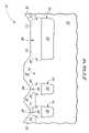
- FIG. 22is a view of the FIG. 21 substrate at a processing step subsequent to that shown by FIG. 21 , and taken through line 22 - 22 in FIG. 23 .
- FIG. 23is a top view of FIG. 22 .
- FIG. 24is a view of the FIG. 22 substrate at a processing step subsequent to that shown by FIG. 22 , and taken through line 24 - 24 in FIG. 25 .
- FIG. 25is a top view of FIG. 24 .
- FIG. 26is a view of the FIG. 24 substrate at a processing step subsequent to that shown by FIG. 24 , and taken through line 26 - 26 in FIG. 27 .
- FIG. 27is a top view of FIG. 26 .
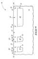
- FIG. 28is a view of the FIG. 26 substrate at a processing step subsequent to that shown by FIG. 26 , and taken through line 28 - 28 in FIG. 29 .
- FIG. 29is a top view of FIG. 28 .
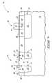
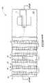
- a fragment of a semiconductive substrateis indicated generally with reference numeral 10 .
- Suchcomprises bulk semiconductive material 12 , which is preferably a bulk semiconductive silicon-comprising material.
- semiconductor substrateor “semiconductive substrate” is defined to mean any construction comprising semiconductive material, including, but not limited to, bulk semiconductive materials such as a semiconductive wafer (either alone or in assemblies comprising other materials thereon), and semiconductive material layers (either alone or in assemblies comprising other materials).
- substraterefers to any supporting structure, including, but not limited to, the semiconductive substrates described above.
- An exemplary preferred material 12includes a lightly p-doped monocrystalline silicon wafer.
- the preferred bulk semiconductive silicon-comprising materialmight include one or more other elements, for example a silicon-germanium mixture and by way of example only. Further, bulk semiconductive material 12 might include one or more localized or more global dopant wells formed therein. Bulk semiconductive silicon-comprising material 12 comprises an outermost surface 15 , which in the depicted preferred embodiment is essentially planar although of course is not required.
- a pad oxide layer 11 and a silicon nitride-comprising masking material 13are formed over, and preferably on, outermost surface 15 (with “on” in the context of this document meaning in at least some direct physical, touching contact therewith).
- a series of isolation trenches 14 , 16 and 18have been formed within bulk semiconductive silicon-comprising material 12 , preferably by etching using the silicon nitride-comprising masking material 13 and pad oxide layer 11 as a mask. Isolation trenches 14 and 16 can be considered as a pair of adjacent isolation trenches, as can isolation trenches 16 and 18 .
- isolation trenches 14 and 16might comprise part of an array area of circuitry, for example a memory array, whereas isolation trench 18 might constitute a separation region for or part of peripheral circuitry to an array of circuitry within which isolation trenches 14 and 16 are received.
- Isolation trenches 14 , 16 and 18might be formed by any existing of yet-to-be developed methods, for example utilizing photolithographic patterning and etch, and/or using the depicted nitride and pad oxide masking layers.
- isolation trenches 14 , 16 and 18comprise shallow trench isolation (STI), with an exemplary trench depth being from surface 15 being from 1,500 Angstroms to 3,000 Angstroms.
- STIshallow trench isolation
- Electrically insulative trench isolation material 20has been formed within isolation trenches 14 , 16 and 18 .
- Suchmight comprise one or more insulative materials.
- suchmight comprise a silicon nitride trench lining having a thermal silicon dioxide layer grown before or after deposition of the silicon nitride lining, and a majority silicon dioxide or other fill thereover, for example deposited by high density plasma deposition or as a spin-on-dielectric.
- materials 11 , 13 and 20have been polished back. Thereby in this example, silicon nitride-comprising masking material 13 has been removed from over outermost surface 15 .
- An exemplary preferred techniqueis by chemical mechanical polishing.
- trench isolation material 20has been etched effective to recess it relative to outermost surface 15 and thereby expose sidewalls 22 , 23 , 24 , 25 , 26 and 27 of bulk semiconductive silicon-comprising material 12 .
- sidewalls 23 and 24are of bulk semiconductive silicon-comprising material 12 between isolation trenches 14 and 16
- sidewalls 25 and 26are of bulk semiconductive silicon-comprising material 12 between isolation trenches 16 and 18 .
- Such etchingforms the depicted recesses 28 , 29 and 30 within bulk semiconductive silicon-comprising material 12 relative to outermost surface 15 over trench isolation material 20 received within the respective isolation trenches.
- An exemplary preferred depth for the recesses from outermost surface 15is at least 200 Angstroms, more preferably at least 500 Angstroms, and even more preferably at least 700 Angstroms, with a preferred range being from 700 Angstroms to 1,500 Angstroms deep from outermost surface 15 .
- Exemplary preferred manners of etching the depicted trench isolation material 20includes a wet hydrofluoric acid etch, a buffered oxide etch (i.e., NH 3 F) or a suitable dry reactive ion etch.
- epitaxially-grown silicon-comprising material 30has been grown from exposed sidewalls 22 , 23 , 24 , 25 , 26 and 27 effective to form epitaxially-grown silicon-comprising material 32 within isolation trenches 28 , 29 and 30 .
- epitaxially-grown silicon-comprising material 32has also been grown therefrom.
- the growinghas been effective to completely fill recesses 28 , 29 and 30 , and also has formed exemplary crystalline stacking faults 33 in part/portions of epitaxially-grown silicon-comprising material 32 , although neither of such is required in certain implementations of the invention.
- stacking faultsmay or may not form, with the depicted exemplary faults propogating elevationally outward from proximate outermost surface 15 from the depicted corners of bulk semiconductive material 12 where the isolation trenches are defined.
- stacking faultscan be eliminated/prevented from forming in the first place where at least silicon nitride-comprising masking material 13 , and preferably pad oxide 11 , are removed prior to growth.
- the epitaxial silicon-comprising materialis void of stacking faults upon its growth.
- exemplary preferred epitaxially-grown silicon-comprising material 32 / 32 zincludes a layer comprising, consisting essentially of, or consisting of monocrystalline silicon. Other materials might of course be encompassed, for example a silicon-germanium mixture/alloy.
- An exemplary preferred process for forming epitaxially-grown silicon-comprising material 32 / 32 zincludes a low pressure chemical vapor deposition process at an exemplary temperature from 500° C.
- a specific exemplary processincludes, in an Applied Materials Centura Processor, a substrate temperature of 850° C., a chamber pressure of 40 Torr, dichlorosilane flow of 0.235 sccm, HCI flow of 166 sccm and H 2 flow at 14 slm.
- epitaxially-grown silicon-comprising material 32has been planarized, for example by chemical mechanical polishing. Stacking faults may or may not exist in the planarized layer in part depending upon whether such were formed in the growth process of FIG. 4 , and where such do occur, and to the degree of material 32 removal. Material 32 might be removed to a point elevationally outward of outermost surface 15 (as shown), to a point at about surface 15 (not shown), or to a point below surface 15 (not shown).
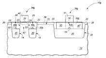
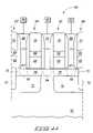
- exemplary field effect transistors 34 and 36have been formed.
- epitaxially-grown silicon-comprising material 32has been patterned, and electrically insulative isolation regions 38 have been formed therebetween.
- An exemplary preferred materialis doped or undoped silicon dioxide.
- Field effect transistors 34 and 36are depicted as comprising respective gates 40 , 41 ; channel regions 42 , 43 ; and source/drain regions 44 , 46 and 45 , 47 .
- a suitable gate dielectric layer 48separates the conductive gates from the respective channel regions.
- Conductive gates 40 , 41might comprise one or a combination of conductively doped semiconductive, metal, and metal compound materials. Insulative caps and spacers might also, of course, be provided.
- the depicted source/drain regionscan be formed by suitable ion implant doping, by way of example only.
- At least a portion of a) at least one of the channel region and b) at least one of the source/drain regionsis received within epitaxially-grown silicon-comprising material 32 .
- portions of the respective channel regions and both source/drain regions of each depicted transistorare received within epitaxially-grown silicon-comprising material 32 .
- field effect transistor 36clearly all of channel region 43 and all of both source/drain regions 45 and 47 of such pair of source/drain regions are received within epitaxially-grown silicon-comprising material 32 over trench isolation material 20 of isolation trench 18 .
- a method of forming a field effect transistorincludes, where crystalline stacking faults are formed, removing part of the epitaxially-grown silicon-comprising material effective to remove the crystalline stacking faults prior to forming that portion of the channel region and/or source/drain regions which are formed or received within the epitaxially-grown silicon-comprising material.
- the stacking faults 33 appearing in FIG. 4 relative to isolation trench 18have effectively been removed such that such do not appear in field effect transistor 36 .
- Field effect transistor 34depicts some of stacking faults 33 remaining, although such might not be formed in the first place, thereby not existing in transistor 34 .
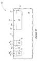
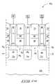
- FIGS. 8 and 9depict an alternate embodiment substrate fragment 10 a .
- Like numerals from the first-described embodimenthave been utilized where appropriate, with differences being indicated with the suffix “a”.
- FIG. 8depicts an alternate processing to that shown by FIG. 6 .
- epitaxially-grown silicon-comprising material 32has been removed at least to bulk semiconductive silicon-comprising material outermost surface 15 , leaving epitaxially-grown silicon-comprising material 32 a within recesses 28 , 29 and 30 .
- Such processingthereby removes all of the depicted stacking faults as shown in FIG. 4 .
- FIG. 9depicts resultant transistors 34 a and 36 a . Such also depicts, by way of example only, an exemplary embodiment where none of channel region 42 a of transistor 34 a is formed within epitaxially-grown silicon-comprising material 32 a , rather being formed within bulk semiconductive silicon-comprising material 12 .
- FIG. 10depicts an alternate exemplary semiconductor wafer fragment 1 O b is depicted. Like numerals from the first-described embodiment have been utilized where appropriate, with differences being indicated with the suffix “b” or with different numerals.
- FIG. 10depicts an exemplary embodiment whereby epitaxially-grown silicon-comprising material has been grown from the exposed sidewalls effective to fill only a portion of recesses 28 , 29 and 30 , leaving respective voids 50 , 52 and 54 within the depicted recesses which are covered by epitaxially-grown silicon-comprising material 32 b and with such voids extending to insulative trench isolation material 20 . Void formation can be induced by factors including deposition thickness, pressure, and temperature.
- lower pressure and faster growth ratefavorably increase the degree of void formation.
- voidsmight be formed in any of the other embodiments described above and elsewhere herein.
- FIG. 8depicts integrated circuitry incorporating field effect transistors 34 b , 36 b , individually comprising a gate, a channel region, and a pair of source/drain regions. At least a portion of at least one of a) the channel region and b) at least one of the source/drain regions is received within the semiconductor material over the insulative material, with such portion comprising a void received within the semiconductor material and extending to the insulative material.
- FIGS. 11 , 12 , 13 and 14depict exemplary alternate embodiments of integrated circuitry in fabrication encompassing dynamic random access memory (DRAM).
- DRAMdynamic random access memory
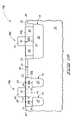
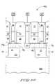
- FIG. 11such depicts an integrated circuit fragment 60 of a semiconductor substrate comprising bulk semiconductive material 62 . Alternate substrates are of course contemplated.
- a series of wordline constructions 63 , 64 , 65 and 66are received over bulk semiconductive material 62 (for example preferably of the same composition as material 12 of the first described embodiment).
- Suchcomprise a gate dielectric layer 67 , conductively doped polysilicon region 68 , conductive metal or metal silicide region 69 , and insulative caps 70 .
- Electrically insulative sidewall spacers 71are received about the respective wordlines as shown.
- Electrically insulative material 72is depicted as being received within bulk semiconductive material 62 .
- material 72comprises electrically insulative trench isolation material, for example fabricated as described above.
- Another insulative trench material 73which might be the same or different from material 72 , is shown for isolating from adjacent other devices not depicted in FIG. 11 .
- a semiconductor material 75has been formed on insulative material 72 .
- An exemplary preferred material 75is epitaxially-grown silicon, for example of a composition and formed in the manners of circuitry fabrication described above.
- Semiconductor material 75might include other materials such as germanium, and regardless might be of the same or different composition from that of semiconductive material 62 .
- Channel regions 76 and 78are depicted as being received beneath wordline constructions 64 and 65 , respectively, within semiconductor material 75 , as are a source/drain region 80 associated with wordline 64 and a source/drain region 82 associated with wordline 65 and within semiconductor material 75 .
- a exemplary shared source/drain region 84is depicted as being received within bulk semiconductive material 62 between wordline constructions 64 and 65 .
- Electrically conductive contacts 86 and 88extend elevationally outward from source/drain regions 80 and 82 , respectively. Such would connect with respective storage node capacitors designated with numerals 90 and 92 .
- a conductive contact 94extends elevationally outward from shared source/drain region 84 and electrically connects with a bitline 95 .
- one field effect transistorcomprises wordline gate construction 64 , source/drain regions 80 and 84 , and channel region 76 .
- Another depicted field effect transistorcomprises wordline gate 65 , source/drain regions 84 and 82 , and channel region 78 .
- one of the source/drain regions of a transistor(of course not necessarily all or more than one transistor) is formed in semiconductor material 75 (i.e., source/drain region 80 ), and the other of the source/drain regions is formed in bulk semiconductive material 62 (i.e., source/drain region 84 ). Accordingly by way of example only, such depicts all of only one of the source/drain regions of the transistor as being received within semiconductor material 75 , for example within epitaxially-grown silicon-comprising material as might be fabricated in accordance with the above-described methods.
- FIG. 12an alternate exemplary embodiment integrated circuit and method of fabrication of a field effect transistor is depicted in FIG. 12 with respect to a semiconductor substrate 60 a .
- the integrated circuit of FIG. 12depicts a field effect transistor wherein the channel region (i.e., channel regions 76 a and 78 a ) is received partially within semiconductor material 75 a and partially within bulk semiconductive material 62 a . Further and regardless, FIG.
- FIG. 12depicts one implementation wherein electrically insulative material 72 a extends from beneath one of the source/drain regions in a transistor (i.e., source/drain regions 80 or 82 ) to beneath only a portion of the channel region (i.e., channel regions 76 a or 78 a ). Therefore, and in accordance with the above-described or other methods of forming a field effect transistor, FIG.
- FIG. 12depicts an implementation whereby at least a part of the channel region is received within the bulk semiconductor silicon-comprising material, for example material 62 a , and also an implementation wherein only a part of a channel region is received within epitaxially-grown silicon-comprising material, depicted in the preferred embodiment and by way of example only, as material 75 a .
- FIG. 13Another alternate embodiment semiconductor substrate 60 b is depicted in FIG. 13 . Like numerals from the FIG. 11 embodiment are utilized where appropriate, with differences being indicated with the suffix “b”. Here, all of channel regions 76 b and 78 b are received within bulk semiconductive material 62 b . Further in the depicted implementation, all of only one of the source/drain regions of each transistor is received within the epitaxially-grown silicon-comprising material, with the other source/drain region (i.e., source/drain region 84 ) being received within bulk semiconductive material.
- FIG. 14Yet another alternate exemplary embodiment semiconductor substrate 60 c is depicted in FIG. 14 .
- Like numerals from the FIG. 11 embodimentare utilized where appropriate, with differences being indicated with the suffix “c”.
- suchdepicts a pseudo-SOI construction whereby source/drain regions 80 , 82 and 84 c are formed within semiconductor material/epitaxially-grown silicon-comprising material 75 c , and at least some of channel regions 76 c and 78 c are comprised of bulk semiconductive material and are also shown as comprising some semiconductor material/epitaxially-grown silicon-comprising material 75 c.
- FIG. 11exemplary methods for fabricating the structure of FIG. 11 are described with reference to FIGS. 15-29 . Processing could be modified, of course, to produce any of the other structures of FIGS. 12-14 , or other structures, in accordance with aspects of the invention, and of course using other or modified methods.
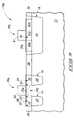
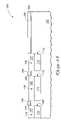
- a semiconductor substrateis indicated generally with reference numeral 100 .
- Suchcomprises bulk semiconductive material 102 , for example and by way of example only, bulk monocrystalline silicon.
- a pad oxide layer 104 and a silicon nitride layer 106have been formed over bulk semiconductive material 102 .
- Suchhave been masked and patterned to form a trench isolation mask, whereby exemplary isolation trenches 108 , 110 and 112 are formed.
- Electrically insulative trench isolation material 114has been formed within isolation trenches 108 , 110 and 112 .
- Suchhas been etched effective to recess it relative to the outermost surface of bulk semiconductive material 102 , thereby leaving recesses 116 , 118 and 120 .
- silicon-nitride comprising masking material 106 and pad oxide layer 104remain at least in part over substrate 102 .
- epitaxially-grown silicon-comprising material 122has been grown from exposed sidewalls of the trenches effective to form epitaxially-grown silicon-comprising material within such trenches.
- An exemplary epitaxially-grown silicon thicknessis 5,000 Angstroms.
- Likely stacking faultsare indicated with numeral 123 .
- epitaxially-grown silicon-comprising material 122has been chemical mechanical polished essentially selective relative to the depicted nitride mask 106 . Such might be slightly over-etched/removed, for example over-removed to about 300 Angstroms.
- masking nitride 106 and pad oxide 104have been removed.
- Preferred processingis by any suitable wet etching.
- FIGS. 19 and 20alternative processing to that depicted by FIGS. 17 and 18 is shown in FIGS. 19 and 20 with respect to a semiconductor substrate 100 a .
- Like numerals from the FIGS. 17 and 18 embodimenthave been utilized where appropriate, with differences being indicated with the suffix “a”.
- FIG. 19epitaxially-grown silicon-comprising material 122 a has been subjected to a suitable timed etch to recess it to below pad oxide 104 . Silicon nitride 106 and pad oxide 104 are subsequently stripped ( FIG. 20 ).
- the epitaxially-grown silicon-comprising material 122 of FIG. 18has been planarized, for example by chemical mechanical polishing.
- FIGS. 22 and 23another pad oxide layer 130 and another silicon nitride masking layer 132 have been deposited and patterned, as shown, for the formation of additional trench isolation.
- additional electrically insulative isolation material 133has been deposited and planarized back, as shown.
- An exemplary preferred materialis silicon dioxide, for example deposited by high density plasma deposition or as a spin-on-dielectric. Silicon nitride or other materials might of course be utilized, as well as other materials.
- silicon nitride 132 and pad oxide 130have been removed, preferably by any suitable wet or other etching.
- substrate 100has been processed essentially to produce the construction shown in FIG. 11 .
Landscapes
- Engineering & Computer Science (AREA)
- Manufacturing & Machinery (AREA)
- Physics & Mathematics (AREA)
- Condensed Matter Physics & Semiconductors (AREA)
- General Physics & Mathematics (AREA)
- Computer Hardware Design (AREA)
- Microelectronics & Electronic Packaging (AREA)
- Power Engineering (AREA)
- Chemical & Material Sciences (AREA)
- Materials Engineering (AREA)
- Crystallography & Structural Chemistry (AREA)
- Insulated Gate Type Field-Effect Transistor (AREA)
- Semiconductor Memories (AREA)
Abstract
Description
Claims (5)
Priority Applications (2)
| Application Number | Priority Date | Filing Date | Title |
|---|---|---|---|
| US11/704,487US7329924B2 (en) | 2005-03-10 | 2007-02-09 | Integrated circuits and methods of forming a field effect transistor |
| US11/957,013US7687857B2 (en) | 2005-03-10 | 2007-12-14 | Integrated circuits |
Applications Claiming Priority (2)
| Application Number | Priority Date | Filing Date | Title |
|---|---|---|---|
| US11/076,774US7244659B2 (en) | 2005-03-10 | 2005-03-10 | Integrated circuits and methods of forming a field effect transistor |
| US11/704,487US7329924B2 (en) | 2005-03-10 | 2007-02-09 | Integrated circuits and methods of forming a field effect transistor |
Related Parent Applications (1)
| Application Number | Title | Priority Date | Filing Date |
|---|---|---|---|
| US11/076,774DivisionUS7244659B2 (en) | 2005-03-10 | 2005-03-10 | Integrated circuits and methods of forming a field effect transistor |
Related Child Applications (1)
| Application Number | Title | Priority Date | Filing Date |
|---|---|---|---|
| US11/957,013DivisionUS7687857B2 (en) | 2005-03-10 | 2007-12-14 | Integrated circuits |
Publications (2)
| Publication Number | Publication Date |
|---|---|
| US20070141771A1 US20070141771A1 (en) | 2007-06-21 |
| US7329924B2true US7329924B2 (en) | 2008-02-12 |
Family
ID=36971537
Family Applications (3)
| Application Number | Title | Priority Date | Filing Date |
|---|---|---|---|
| US11/076,774Active2025-10-29US7244659B2 (en) | 2005-03-10 | 2005-03-10 | Integrated circuits and methods of forming a field effect transistor |
| US11/704,487Expired - LifetimeUS7329924B2 (en) | 2005-03-10 | 2007-02-09 | Integrated circuits and methods of forming a field effect transistor |
| US11/957,013Expired - LifetimeUS7687857B2 (en) | 2005-03-10 | 2007-12-14 | Integrated circuits |
Family Applications Before (1)
| Application Number | Title | Priority Date | Filing Date |
|---|---|---|---|
| US11/076,774Active2025-10-29US7244659B2 (en) | 2005-03-10 | 2005-03-10 | Integrated circuits and methods of forming a field effect transistor |
Family Applications After (1)
| Application Number | Title | Priority Date | Filing Date |
|---|---|---|---|
| US11/957,013Expired - LifetimeUS7687857B2 (en) | 2005-03-10 | 2007-12-14 | Integrated circuits |
Country Status (1)
| Country | Link |
|---|---|
| US (3) | US7244659B2 (en) |
Families Citing this family (28)
| Publication number | Priority date | Publication date | Assignee | Title |
|---|---|---|---|---|
| US5977579A (en)* | 1998-12-03 | 1999-11-02 | Micron Technology, Inc. | Trench dram cell with vertical device and buried word lines |
| US7071043B2 (en)* | 2002-08-15 | 2006-07-04 | Micron Technology, Inc. | Methods of forming a field effect transistor having source/drain material over insulative material |
| US6844591B1 (en)* | 2003-09-17 | 2005-01-18 | Micron Technology, Inc. | Method of forming DRAM access transistors |
| US7262089B2 (en)* | 2004-03-11 | 2007-08-28 | Micron Technology, Inc. | Methods of forming semiconductor structures |
| US7518182B2 (en)* | 2004-07-20 | 2009-04-14 | Micron Technology, Inc. | DRAM layout with vertical FETs and method of formation |
| US7547945B2 (en) | 2004-09-01 | 2009-06-16 | Micron Technology, Inc. | Transistor devices, transistor structures and semiconductor constructions |
| US7244659B2 (en)* | 2005-03-10 | 2007-07-17 | Micron Technology, Inc. | Integrated circuits and methods of forming a field effect transistor |
| US7384849B2 (en)* | 2005-03-25 | 2008-06-10 | Micron Technology, Inc. | Methods of forming recessed access devices associated with semiconductor constructions |
| US7282401B2 (en) | 2005-07-08 | 2007-10-16 | Micron Technology, Inc. | Method and apparatus for a self-aligned recessed access device (RAD) transistor gate |
| US7867851B2 (en)* | 2005-08-30 | 2011-01-11 | Micron Technology, Inc. | Methods of forming field effect transistors on substrates |
| US7867845B2 (en)* | 2005-09-01 | 2011-01-11 | Micron Technology, Inc. | Transistor gate forming methods and transistor structures |
| US7564081B2 (en) | 2005-11-30 | 2009-07-21 | International Business Machines Corporation | finFET structure with multiply stressed gate electrode |
| US7700441B2 (en) | 2006-02-02 | 2010-04-20 | Micron Technology, Inc. | Methods of forming field effect transistors, methods of forming field effect transistor gates, methods of forming integrated circuitry comprising a transistor gate array and circuitry peripheral to the gate array, and methods of forming integrated circuitry comprising a transistor gate array including first gates and second grounded isolation gates |
| US8008144B2 (en) | 2006-05-11 | 2011-08-30 | Micron Technology, Inc. | Dual work function recessed access device and methods of forming |
| US20070262395A1 (en)* | 2006-05-11 | 2007-11-15 | Gibbons Jasper S | Memory cell access devices and methods of making the same |
| US8860174B2 (en)* | 2006-05-11 | 2014-10-14 | Micron Technology, Inc. | Recessed antifuse structures and methods of making the same |
| US7602001B2 (en) | 2006-07-17 | 2009-10-13 | Micron Technology, Inc. | Capacitorless one transistor DRAM cell, integrated circuitry comprising an array of capacitorless one transistor DRAM cells, and method of forming lines of capacitorless one transistor DRAM cells |
| US7772632B2 (en) | 2006-08-21 | 2010-08-10 | Micron Technology, Inc. | Memory arrays and methods of fabricating memory arrays |
| US7589995B2 (en) | 2006-09-07 | 2009-09-15 | Micron Technology, Inc. | One-transistor memory cell with bias gate |
| US7923373B2 (en) | 2007-06-04 | 2011-04-12 | Micron Technology, Inc. | Pitch multiplication using self-assembling materials |
| KR101414076B1 (en)* | 2008-09-10 | 2014-07-02 | 삼성전자주식회사 | Semiconductor device and method for manufacturing the same |
| US7824986B2 (en) | 2008-11-05 | 2010-11-02 | Micron Technology, Inc. | Methods of forming a plurality of transistor gates, and methods of forming a plurality of transistor gates having at least two different work functions |
| US20100187660A1 (en)* | 2009-01-26 | 2010-07-29 | Sanh Tang | Method To Create SOI Layer For 3D-Stacking Memory Array |
| US8227304B2 (en)* | 2010-02-23 | 2012-07-24 | International Business Machines Corporation | Semiconductor-on-insulator (SOI) structure and method of forming the SOI structure using a bulk semiconductor starting wafer |
| US9401363B2 (en) | 2011-08-23 | 2016-07-26 | Micron Technology, Inc. | Vertical transistor devices, memory arrays, and methods of forming vertical transistor devices |
| US10109638B1 (en)* | 2017-10-23 | 2018-10-23 | Globalfoundries Singapore Pte. Ltd. | Embedded non-volatile memory (NVM) on fully depleted silicon-on-insulator (FD-SOI) substrate |
| US11315838B2 (en) | 2018-09-28 | 2022-04-26 | Taiwan Semiconductor Manufacturing Company, Ltd. | FinFET device and method of forming same |
| CN110970487B (en)* | 2018-09-28 | 2023-12-19 | 台湾积体电路制造股份有限公司 | Semiconductor devices and methods of forming the same |
Citations (53)
| Publication number | Priority date | Publication date | Assignee | Title |
|---|---|---|---|---|
| US4820654A (en) | 1987-12-09 | 1989-04-11 | Ncr Corporation | Isolation of regions in a CMOS structure using selective epitaxial growth |
| US5021843A (en) | 1983-08-25 | 1991-06-04 | Tadahiro Ohmi | Semiconductor integrated circuit |
| US5374329A (en) | 1992-01-31 | 1994-12-20 | Canon Kabushiki Kaisha | Process for producing a semiconductor wafer |
| US5405802A (en) | 1992-01-31 | 1995-04-11 | Canon Kabushiki Kaisha | Process of fabricating a semiconductor substrate |
| US5453394A (en) | 1992-01-31 | 1995-09-26 | Canon Kabushiki Kaisha | Process for preparing semiconductor substrate by bringing first and second substrates in contact |
| US5767020A (en) | 1991-02-15 | 1998-06-16 | Canon Kabushiki Kaisha | Etching solution for etching porous silicon, etching method using the etching solution and method of preparing semiconductor member using the etching solution |
| US5773355A (en) | 1994-04-08 | 1998-06-30 | Canon Kabushiki Kaisha | Method for manufacturing semiconductor substrate |
| US5841171A (en) | 1996-05-08 | 1998-11-24 | Mitsubishi Denki Kabushiki Kaisha | SOI Semiconductor devices |
| US5849627A (en) | 1990-02-07 | 1998-12-15 | Harris Corporation | Bonded wafer processing with oxidative bonding |
| US5882532A (en) | 1996-05-31 | 1999-03-16 | Hewlett-Packard Company | Fabrication of single-crystal silicon structures using sacrificial-layer wafer bonding |
| US5910672A (en) | 1997-02-26 | 1999-06-08 | Mitsubishi Denki Kabushiki Kaisha | Semiconductor device and method of manufacturing the same |
| US6010921A (en) | 1997-05-23 | 2000-01-04 | Sharp Kabushiki Kaisha | Method of fabricating a field-effect transistor utilizing an SOI substrate |
| US6037634A (en) | 1996-02-02 | 2000-03-14 | Mitsubishi Denki Kabushiki Kaisha | Semiconductor device with first and second elements formed on first and second portions |
| US6048411A (en) | 1997-05-12 | 2000-04-11 | Silicon Genesis Corporation | Silicon-on-silicon hybrid wafer assembly |
| US6071783A (en) | 1998-08-13 | 2000-06-06 | Taiwan Semiconductor Manufacturing Company | Pseudo silicon on insulator MOSFET device |
| US6091076A (en) | 1996-06-14 | 2000-07-18 | Commissariat A L'energie Atomique | Quantum WELL MOS transistor and methods for making same |
| US6147384A (en)* | 1996-12-19 | 2000-11-14 | Texas Instruments Incorporated | Method for forming planar field effect transistors with source and drain an insulator and device constructed therefrom |
| US6215155B1 (en) | 1997-12-19 | 2001-04-10 | Advanced Micro Devices, Inc. | Silicon-on-insulator configuration which is compatible with bulk CMOS architecture |
| US6245636B1 (en) | 1999-10-20 | 2001-06-12 | Advanced Micro Devices, Inc. | Method of formation of pseudo-SOI structures with direct contact of transistor body to the substrate |
| US6255731B1 (en) | 1997-07-30 | 2001-07-03 | Canon Kabushiki Kaisha | SOI bonding structure |
| US6265327B1 (en) | 1997-06-20 | 2001-07-24 | Japan Science And Technology Corp. | Method for forming an insulating film on semiconductor substrate surface and apparatus for carrying out the method |
| US6268630B1 (en) | 1999-03-16 | 2001-07-31 | Sandia Corporation | Silicon-on-insulator field effect transistor with improved body ties for rad-hard applications |
| US20010020722A1 (en) | 2000-03-07 | 2001-09-13 | Chien-Kuo Yang | Step-like silicon on isolation structure |
| US6313014B1 (en) | 1998-06-18 | 2001-11-06 | Canon Kabushiki Kaisha | Semiconductor substrate and manufacturing method of semiconductor substrate |
| US6340829B1 (en) | 1998-05-06 | 2002-01-22 | Mitsubishi Denki Kabushiki Kaisha | Semiconductor device and method for manufacturing the same |
| US20020011670A1 (en) | 2000-06-30 | 2002-01-31 | Kabushiki Kaisha Toshiba | Semiconductor device manufacturing method including forming step of SOI structure and semiconductor device having SOI structure |
| US6350703B1 (en) | 1998-07-08 | 2002-02-26 | Canon Kabushiki Kaisha | Semiconductor substrate and production method thereof |
| US6358791B1 (en) | 1999-06-04 | 2002-03-19 | International Business Machines Corporation | Method for increasing a very-large-scale-integrated (VLSI) capacitor size on bulk silicon and silicon-on-insulator (SOI) wafers and structure formed thereby |
| US6362082B1 (en)* | 1999-06-28 | 2002-03-26 | Intel Corporation | Methodology for control of short channel effects in MOS transistors |
| US20020048844A1 (en) | 2000-10-25 | 2002-04-25 | Kiyofumi Sakaguchi | Semiconductor substrate, method of manufacturing the same, and bonded substrate stack surface shape measuring method |
| US6403485B1 (en) | 2001-05-02 | 2002-06-11 | Chartered Semiconductor Manufacturing Ltd | Method to form a low parasitic capacitance pseudo-SOI CMOS device |
| US20020070454A1 (en) | 2000-11-30 | 2002-06-13 | Seiko Epson Corporation | SOI substrate, element substrate, semiconductor device, electro-optical apparatus, electronic equipment, method of manufacturing the SOI substrate, method of manufacturing the element substrate, and method of manufacturing the electro-optical apparatus |
| US6410938B1 (en) | 2001-04-03 | 2002-06-25 | Advanced Micro Devices, Inc. | Semiconductor-on-insulator device with nitrided buried oxide and method of fabricating |
| US6433401B1 (en) | 1999-04-06 | 2002-08-13 | Analog Devices Imi, Inc. | Microfabricated structures with trench-isolation using bonded-substrates and cavities |
| US20020134503A1 (en) | 2001-03-20 | 2002-09-26 | Accucorp Technical Services, Inc. | Silicon wafers bonded to insulator substrates by low viscosity epoxy wicking |
| US6509613B1 (en) | 2001-05-04 | 2003-01-21 | Advanced Micro Devices, Inc. | Self-aligned floating body control for SOI device through leakage enhanced buried oxide |
| US6512244B1 (en) | 2001-05-07 | 2003-01-28 | Advanced Micro Devices, Inc. | SOI device with structure for enhancing carrier recombination and method of fabricating same |
| US6531375B1 (en) | 2001-09-18 | 2003-03-11 | International Business Machines Corporation | Method of forming a body contact using BOX modification |
| US6534380B1 (en) | 1997-07-18 | 2003-03-18 | Denso Corporation | Semiconductor substrate and method of manufacturing the same |
| US6552496B2 (en) | 1999-06-28 | 2003-04-22 | Semiconductor Energy Laboratory Co., Ltd. | EL display device and electronic device |
| US6552396B1 (en) | 2000-03-14 | 2003-04-22 | International Business Machines Corporation | Matched transistors and methods for forming the same |
| US20030085424A1 (en) | 2001-11-02 | 2003-05-08 | International Business Machines Corporation | Transistor structure with thick recessed source/drain structures and fabrication process of same |
| US6570217B1 (en)* | 1998-04-24 | 2003-05-27 | Kabushiki Kaisha Toshiba | Semiconductor device and method of manufacturing the same |
| US6599789B1 (en)* | 2000-11-15 | 2003-07-29 | Micron Technology, Inc. | Method of forming a field effect transistor |
| US6610615B1 (en) | 2000-11-15 | 2003-08-26 | Intel Corporation | Plasma nitridation for reduced leakage gate dielectric layers |
| US6642579B2 (en) | 2001-08-28 | 2003-11-04 | International Business Machines Corporation | Method of reducing the extrinsic body resistance in a silicon-on-insulator body contacted MOSFET |
| US6661065B2 (en) | 2000-09-01 | 2003-12-09 | Mitsubishi Denki Kabushiki Kaisha | Semiconductor device and SOI substrate |
| US6664146B1 (en) | 2001-06-01 | 2003-12-16 | Advanced Micro Devices, Inc. | Integration of fully depleted and partially depleted field effect transistors formed in SOI technology |
| US6680243B1 (en) | 2001-06-29 | 2004-01-20 | Lsi Logic Corporation | Shallow junction formation |
| US6683364B2 (en) | 2001-07-13 | 2004-01-27 | Samsung Electronics Co., Ltd. | Integrated circuit devices including an isolation region defining an active region area and methods for manufacturing the same |
| US20050062080A1 (en)* | 2003-09-24 | 2005-03-24 | Fujitsu Limited | Semiconductor device and method of manufacturing same |
| US20050176222A1 (en)* | 2002-05-08 | 2005-08-11 | Atsushi Ogura | Semiconductor substrate manufacturing method and semiconductor device manufacturing method, and semiconductor substrate and semiconductor device manufactured by the methods |
| US7029989B2 (en) | 2002-10-14 | 2006-04-18 | Hynix Semiconductor Inc. | Semiconductor device and method of manufacturing the same |
Family Cites Families (29)
| Publication number | Priority date | Publication date | Assignee | Title |
|---|---|---|---|---|
| US5013680A (en)* | 1990-07-18 | 1991-05-07 | Micron Technology, Inc. | Process for fabricating a DRAM array having feature widths that transcend the resolution limit of available photolithography |
| US5122848A (en)* | 1991-04-08 | 1992-06-16 | Micron Technology, Inc. | Insulated-gate vertical field-effect transistor with high current drive and minimum overlap capacitance |
| US5676020A (en)* | 1995-06-30 | 1997-10-14 | Sram Corporation | Hand-rotatable bicycle gear shift actuator with overshift return |
| US6150687A (en)* | 1997-07-08 | 2000-11-21 | Micron Technology, Inc. | Memory cell having a vertical transistor with buried source/drain and dual gates |
| US6191470B1 (en)* | 1997-07-08 | 2001-02-20 | Micron Technology, Inc. | Semiconductor-on-insulator memory cell with buried word and body lines |
| US5909618A (en)* | 1997-07-08 | 1999-06-01 | Micron Technology, Inc. | Method of making memory cell with vertical transistor and buried word and body lines |
| US6072209A (en)* | 1997-07-08 | 2000-06-06 | Micro Technology, Inc. | Four F2 folded bit line DRAM cell structure having buried bit and word lines |
| US5963469A (en)* | 1998-02-24 | 1999-10-05 | Micron Technology, Inc. | Vertical bipolar read access for low voltage memory cell |
| US6696746B1 (en)* | 1998-04-29 | 2004-02-24 | Micron Technology, Inc. | Buried conductors |
| US5977579A (en)* | 1998-12-03 | 1999-11-02 | Micron Technology, Inc. | Trench dram cell with vertical device and buried word lines |
| FR2797640B1 (en)* | 1999-08-17 | 2001-09-21 | Inst Francais Du Petrole | METHOD AND DEVICE FOR SEPARATING ETHANE AND ETHYLENE FROM A STEAM CRACKING EFFLUENT BY SOLVENT ABSORPTION AND HYDROGENATION OF THE SOLVENT PHASE |
| KR100344282B1 (en)* | 1999-10-30 | 2002-07-24 | 주식회사 신동방 | Method of making isoflavone aglucone using rhodotorula glutinis having ability to produce isoflavone aglucone |
| US6510938B1 (en)* | 2000-11-28 | 2003-01-28 | Delaware Capital Formation, Inc. | Soft touch infeed |
| US6498062B2 (en)* | 2001-04-27 | 2002-12-24 | Micron Technology, Inc. | DRAM access transistor |
| JP2003243528A (en)* | 2002-02-13 | 2003-08-29 | Toshiba Corp | Semiconductor device |
| US7071043B2 (en)* | 2002-08-15 | 2006-07-04 | Micron Technology, Inc. | Methods of forming a field effect transistor having source/drain material over insulative material |
| JP3974542B2 (en)* | 2003-03-17 | 2007-09-12 | 株式会社東芝 | Semiconductor substrate manufacturing method and semiconductor device manufacturing method |
| US6844591B1 (en)* | 2003-09-17 | 2005-01-18 | Micron Technology, Inc. | Method of forming DRAM access transistors |
| US20050104156A1 (en)* | 2003-11-13 | 2005-05-19 | Texas Instruments Incorporated | Forming a semiconductor structure in manufacturing a semiconductor device using one or more epitaxial growth processes |
| KR100521383B1 (en)* | 2003-11-17 | 2005-10-12 | 삼성전자주식회사 | Semiconductor device with source/drain formed on isolation layers and method of fabricating the same |
| US7262089B2 (en)* | 2004-03-11 | 2007-08-28 | Micron Technology, Inc. | Methods of forming semiconductor structures |
| US7122425B2 (en)* | 2004-08-24 | 2006-10-17 | Micron Technology, Inc. | Methods of forming semiconductor constructions |
| US7335963B2 (en)* | 2004-08-25 | 2008-02-26 | Micron Technology, Inc. | Light block for pixel arrays |
| US7285812B2 (en)* | 2004-09-02 | 2007-10-23 | Micron Technology, Inc. | Vertical transistors |
| US7244659B2 (en)* | 2005-03-10 | 2007-07-17 | Micron Technology, Inc. | Integrated circuits and methods of forming a field effect transistor |
| US7384849B2 (en)* | 2005-03-25 | 2008-06-10 | Micron Technology, Inc. | Methods of forming recessed access devices associated with semiconductor constructions |
| US7214621B2 (en)* | 2005-05-18 | 2007-05-08 | Micron Technology, Inc. | Methods of forming devices associated with semiconductor constructions |
| US7282401B2 (en)* | 2005-07-08 | 2007-10-16 | Micron Technology, Inc. | Method and apparatus for a self-aligned recessed access device (RAD) transistor gate |
| US7349232B2 (en)* | 2006-03-15 | 2008-03-25 | Micron Technology, Inc. | 6F2 DRAM cell design with 3F-pitch folded digitline sense amplifier |
- 2005
- 2005-03-10USUS11/076,774patent/US7244659B2/enactiveActive
- 2007
- 2007-02-09USUS11/704,487patent/US7329924B2/ennot_activeExpired - Lifetime
- 2007-12-14USUS11/957,013patent/US7687857B2/ennot_activeExpired - Lifetime
Patent Citations (58)
| Publication number | Priority date | Publication date | Assignee | Title |
|---|---|---|---|---|
| US5021843A (en) | 1983-08-25 | 1991-06-04 | Tadahiro Ohmi | Semiconductor integrated circuit |
| US4820654A (en) | 1987-12-09 | 1989-04-11 | Ncr Corporation | Isolation of regions in a CMOS structure using selective epitaxial growth |
| US5849627A (en) | 1990-02-07 | 1998-12-15 | Harris Corporation | Bonded wafer processing with oxidative bonding |
| US5767020A (en) | 1991-02-15 | 1998-06-16 | Canon Kabushiki Kaisha | Etching solution for etching porous silicon, etching method using the etching solution and method of preparing semiconductor member using the etching solution |
| US5453394A (en) | 1992-01-31 | 1995-09-26 | Canon Kabushiki Kaisha | Process for preparing semiconductor substrate by bringing first and second substrates in contact |
| US5670411A (en) | 1992-01-31 | 1997-09-23 | Canon Kabushiki Kaisha | Process of making semiconductor-on-insulator substrate |
| US5405802A (en) | 1992-01-31 | 1995-04-11 | Canon Kabushiki Kaisha | Process of fabricating a semiconductor substrate |
| US5374329A (en) | 1992-01-31 | 1994-12-20 | Canon Kabushiki Kaisha | Process for producing a semiconductor wafer |
| US5773355A (en) | 1994-04-08 | 1998-06-30 | Canon Kabushiki Kaisha | Method for manufacturing semiconductor substrate |
| US6037634A (en) | 1996-02-02 | 2000-03-14 | Mitsubishi Denki Kabushiki Kaisha | Semiconductor device with first and second elements formed on first and second portions |
| US5841171A (en) | 1996-05-08 | 1998-11-24 | Mitsubishi Denki Kabushiki Kaisha | SOI Semiconductor devices |
| US5882532A (en) | 1996-05-31 | 1999-03-16 | Hewlett-Packard Company | Fabrication of single-crystal silicon structures using sacrificial-layer wafer bonding |
| US6091076A (en) | 1996-06-14 | 2000-07-18 | Commissariat A L'energie Atomique | Quantum WELL MOS transistor and methods for making same |
| US6147384A (en)* | 1996-12-19 | 2000-11-14 | Texas Instruments Incorporated | Method for forming planar field effect transistors with source and drain an insulator and device constructed therefrom |
| US5910672A (en) | 1997-02-26 | 1999-06-08 | Mitsubishi Denki Kabushiki Kaisha | Semiconductor device and method of manufacturing the same |
| US6048411A (en) | 1997-05-12 | 2000-04-11 | Silicon Genesis Corporation | Silicon-on-silicon hybrid wafer assembly |
| US6010921A (en) | 1997-05-23 | 2000-01-04 | Sharp Kabushiki Kaisha | Method of fabricating a field-effect transistor utilizing an SOI substrate |
| US6265327B1 (en) | 1997-06-20 | 2001-07-24 | Japan Science And Technology Corp. | Method for forming an insulating film on semiconductor substrate surface and apparatus for carrying out the method |
| US6534380B1 (en) | 1997-07-18 | 2003-03-18 | Denso Corporation | Semiconductor substrate and method of manufacturing the same |
| US6255731B1 (en) | 1997-07-30 | 2001-07-03 | Canon Kabushiki Kaisha | SOI bonding structure |
| US6215155B1 (en) | 1997-12-19 | 2001-04-10 | Advanced Micro Devices, Inc. | Silicon-on-insulator configuration which is compatible with bulk CMOS architecture |
| US6570217B1 (en)* | 1998-04-24 | 2003-05-27 | Kabushiki Kaisha Toshiba | Semiconductor device and method of manufacturing the same |
| US6340829B1 (en) | 1998-05-06 | 2002-01-22 | Mitsubishi Denki Kabushiki Kaisha | Semiconductor device and method for manufacturing the same |
| US6313014B1 (en) | 1998-06-18 | 2001-11-06 | Canon Kabushiki Kaisha | Semiconductor substrate and manufacturing method of semiconductor substrate |
| US6350703B1 (en) | 1998-07-08 | 2002-02-26 | Canon Kabushiki Kaisha | Semiconductor substrate and production method thereof |
| US6346729B1 (en) | 1998-08-13 | 2002-02-12 | Taiwan Semiconductor Manufacturing Company | Pseudo silicon on insulator MOSFET device |
| US6071783A (en) | 1998-08-13 | 2000-06-06 | Taiwan Semiconductor Manufacturing Company | Pseudo silicon on insulator MOSFET device |
| US6268630B1 (en) | 1999-03-16 | 2001-07-31 | Sandia Corporation | Silicon-on-insulator field effect transistor with improved body ties for rad-hard applications |
| US6433401B1 (en) | 1999-04-06 | 2002-08-13 | Analog Devices Imi, Inc. | Microfabricated structures with trench-isolation using bonded-substrates and cavities |
| US6358791B1 (en) | 1999-06-04 | 2002-03-19 | International Business Machines Corporation | Method for increasing a very-large-scale-integrated (VLSI) capacitor size on bulk silicon and silicon-on-insulator (SOI) wafers and structure formed thereby |
| US20020034844A1 (en) | 1999-06-04 | 2002-03-21 | Hsu Louis L. | Method for increasing a very-large-scale-integrated (VLSI) capacitor size on bulk silicon and silicon-on-insulator (SOI) wafers and structure formed thereby |
| US6649959B2 (en) | 1999-06-04 | 2003-11-18 | International Business Machines Corporation | Method for increasing a very-large-scale-integrated (VLSI) capacitor size on bulk silicon and silicon-on-insulator (SOI) wafers and structure formed thereby |
| US6362082B1 (en)* | 1999-06-28 | 2002-03-26 | Intel Corporation | Methodology for control of short channel effects in MOS transistors |
| US6552496B2 (en) | 1999-06-28 | 2003-04-22 | Semiconductor Energy Laboratory Co., Ltd. | EL display device and electronic device |
| US6245636B1 (en) | 1999-10-20 | 2001-06-12 | Advanced Micro Devices, Inc. | Method of formation of pseudo-SOI structures with direct contact of transistor body to the substrate |
| US20010020722A1 (en) | 2000-03-07 | 2001-09-13 | Chien-Kuo Yang | Step-like silicon on isolation structure |
| US6552396B1 (en) | 2000-03-14 | 2003-04-22 | International Business Machines Corporation | Matched transistors and methods for forming the same |
| US6541861B2 (en) | 2000-06-30 | 2003-04-01 | Kabushiki Kaisha Toshiba | Semiconductor device manufacturing method including forming step of SOI structure and semiconductor device having SOI structure |
| US20020011670A1 (en) | 2000-06-30 | 2002-01-31 | Kabushiki Kaisha Toshiba | Semiconductor device manufacturing method including forming step of SOI structure and semiconductor device having SOI structure |
| US6661065B2 (en) | 2000-09-01 | 2003-12-09 | Mitsubishi Denki Kabushiki Kaisha | Semiconductor device and SOI substrate |
| US20020048844A1 (en) | 2000-10-25 | 2002-04-25 | Kiyofumi Sakaguchi | Semiconductor substrate, method of manufacturing the same, and bonded substrate stack surface shape measuring method |
| US6599789B1 (en)* | 2000-11-15 | 2003-07-29 | Micron Technology, Inc. | Method of forming a field effect transistor |
| US6610615B1 (en) | 2000-11-15 | 2003-08-26 | Intel Corporation | Plasma nitridation for reduced leakage gate dielectric layers |
| US20020070454A1 (en) | 2000-11-30 | 2002-06-13 | Seiko Epson Corporation | SOI substrate, element substrate, semiconductor device, electro-optical apparatus, electronic equipment, method of manufacturing the SOI substrate, method of manufacturing the element substrate, and method of manufacturing the electro-optical apparatus |
| US20020134503A1 (en) | 2001-03-20 | 2002-09-26 | Accucorp Technical Services, Inc. | Silicon wafers bonded to insulator substrates by low viscosity epoxy wicking |
| US6410938B1 (en) | 2001-04-03 | 2002-06-25 | Advanced Micro Devices, Inc. | Semiconductor-on-insulator device with nitrided buried oxide and method of fabricating |
| US6403485B1 (en) | 2001-05-02 | 2002-06-11 | Chartered Semiconductor Manufacturing Ltd | Method to form a low parasitic capacitance pseudo-SOI CMOS device |
| US6509613B1 (en) | 2001-05-04 | 2003-01-21 | Advanced Micro Devices, Inc. | Self-aligned floating body control for SOI device through leakage enhanced buried oxide |
| US6512244B1 (en) | 2001-05-07 | 2003-01-28 | Advanced Micro Devices, Inc. | SOI device with structure for enhancing carrier recombination and method of fabricating same |
| US6664146B1 (en) | 2001-06-01 | 2003-12-16 | Advanced Micro Devices, Inc. | Integration of fully depleted and partially depleted field effect transistors formed in SOI technology |
| US6680243B1 (en) | 2001-06-29 | 2004-01-20 | Lsi Logic Corporation | Shallow junction formation |
| US6683364B2 (en) | 2001-07-13 | 2004-01-27 | Samsung Electronics Co., Ltd. | Integrated circuit devices including an isolation region defining an active region area and methods for manufacturing the same |
| US6642579B2 (en) | 2001-08-28 | 2003-11-04 | International Business Machines Corporation | Method of reducing the extrinsic body resistance in a silicon-on-insulator body contacted MOSFET |
| US6531375B1 (en) | 2001-09-18 | 2003-03-11 | International Business Machines Corporation | Method of forming a body contact using BOX modification |
| US20030085424A1 (en) | 2001-11-02 | 2003-05-08 | International Business Machines Corporation | Transistor structure with thick recessed source/drain structures and fabrication process of same |
| US20050176222A1 (en)* | 2002-05-08 | 2005-08-11 | Atsushi Ogura | Semiconductor substrate manufacturing method and semiconductor device manufacturing method, and semiconductor substrate and semiconductor device manufactured by the methods |
| US7029989B2 (en) | 2002-10-14 | 2006-04-18 | Hynix Semiconductor Inc. | Semiconductor device and method of manufacturing the same |
| US20050062080A1 (en)* | 2003-09-24 | 2005-03-24 | Fujitsu Limited | Semiconductor device and method of manufacturing same |
Non-Patent Citations (7)
| Title |
|---|
| Bashir et al., Characterization of sidewall defects in selective epitaxial growth of silicon, 13 J. Vac Sci. Technol. B, No. 3, pp. 923-927 (May/Jun. 1995). |
| Bashir et al., Reduction of sidewall defect induced leakage currents by the use of nitrided field oxides in silicon selective epitaxial growth . . . , 18 J. Vac. Sci. Technol. B, No. 2, pp. 695-699 (Mar./Apr. 2000). |
| Bernstein et al., ,Ch. 3: SOI Device Electrical Properties, § 3.4 Floating Body Effects, SOI Circuit Design Concepts, pp. 34-53 (Kluwer Academic Publishers, pre-Aug. 2001). |
| Hammad et al., The Pseudo-Two-Dimensional Approach to Model the Drain Section in SOI MOSFETs, 48 IEEE Transactions on Electron Devices, No. 2, pp. 386-387 (Feb. 2001). |
| Sivagnaname et al., Stand-by Current in PD-SOI Pseudo-nMOS Circuits, IEEE, pp. 95-96 (2003). |
| U.S. Appl. No. 10/924,776, filed Aug. 2004, Ford. |
| Wang et al., Achieving Low Junction Capacitance on Bulk SI MOSFET Using SDOI Process, Micron Technology, Inc., 12 pages (pre-2004). |
Also Published As
| Publication number | Publication date |
|---|---|
| US20080099847A1 (en) | 2008-05-01 |
| US7687857B2 (en) | 2010-03-30 |
| US20070141771A1 (en) | 2007-06-21 |
| US7244659B2 (en) | 2007-07-17 |
| US20060205128A1 (en) | 2006-09-14 |
Similar Documents
| Publication | Publication Date | Title |
|---|---|---|
| US7329924B2 (en) | Integrated circuits and methods of forming a field effect transistor | |
| KR100282452B1 (en) | Semiconductor device and method for fabricating the same | |
| US7897460B2 (en) | Methods of forming recessed access devices associated with semiconductor constructions | |
| KR100499159B1 (en) | Semiconductor device having a recessed channel and method of manufacturing the same | |
| KR100340878B1 (en) | Method for fabricating soi device | |
| US6979631B2 (en) | Methods of forming semiconductor circuitry | |
| US20050250279A1 (en) | Methods of forming semiconductor devices having buried oxide patterns and devices related thereto | |
| JP2005536893A (en) | Semiconductor structure | |
| JP2008521251A (en) | Trench capacitors with composite surface-oriented substrates | |
| KR100487564B1 (en) | Semiconductor device having elevated source/drain regions and method of fabricating the same | |
| US6319772B1 (en) | Method for making low-leakage DRAM structures using selective silicon epitaxial growth (SEG) on an insulating layer | |
| JP2004023106A (en) | Semiconductor device and manufacturing method thereof | |
| US6326272B1 (en) | Method for forming self-aligned elevated transistor | |
| KR100517328B1 (en) | Semiconductor device having contact plug using selective epitaxial growth and method of fabricating the same | |
| JP2006303402A (en) | Forming method of contact of semiconductor device using solid phase epitaxial system | |
| JP4524190B2 (en) | Method for manufacturing a semiconductor structure | |
| KR100524802B1 (en) | Semiconductor device having contact plug formed using double selective epitaxial growth and method for fabrication of the same | |
| JP3795347B2 (en) | Method for forming buried contact zone | |
| US20100059852A1 (en) | Semiconductor transistor device with improved isolation arrangement, and related fabrication methods |
Legal Events
| Date | Code | Title | Description |
|---|---|---|---|
| FEPP | Fee payment procedure | Free format text:PAYOR NUMBER ASSIGNED (ORIGINAL EVENT CODE: ASPN); ENTITY STATUS OF PATENT OWNER: LARGE ENTITY | |
| STCF | Information on status: patent grant | Free format text:PATENTED CASE | |
| FPAY | Fee payment | Year of fee payment:4 | |
| FPAY | Fee payment | Year of fee payment:8 | |
| AS | Assignment | Owner name:U.S. BANK NATIONAL ASSOCIATION, AS COLLATERAL AGENT, CALIFORNIA Free format text:SECURITY INTEREST;ASSIGNOR:MICRON TECHNOLOGY, INC.;REEL/FRAME:038669/0001 Effective date:20160426 Owner name:U.S. BANK NATIONAL ASSOCIATION, AS COLLATERAL AGEN Free format text:SECURITY INTEREST;ASSIGNOR:MICRON TECHNOLOGY, INC.;REEL/FRAME:038669/0001 Effective date:20160426 | |
| AS | Assignment | Owner name:MORGAN STANLEY SENIOR FUNDING, INC., AS COLLATERAL AGENT, MARYLAND Free format text:PATENT SECURITY AGREEMENT;ASSIGNOR:MICRON TECHNOLOGY, INC.;REEL/FRAME:038954/0001 Effective date:20160426 Owner name:MORGAN STANLEY SENIOR FUNDING, INC., AS COLLATERAL Free format text:PATENT SECURITY AGREEMENT;ASSIGNOR:MICRON TECHNOLOGY, INC.;REEL/FRAME:038954/0001 Effective date:20160426 | |
| AS | Assignment | Owner name:U.S. BANK NATIONAL ASSOCIATION, AS COLLATERAL AGENT, CALIFORNIA Free format text:CORRECTIVE ASSIGNMENT TO CORRECT THE REPLACE ERRONEOUSLY FILED PATENT #7358718 WITH THE CORRECT PATENT #7358178 PREVIOUSLY RECORDED ON REEL 038669 FRAME 0001. ASSIGNOR(S) HEREBY CONFIRMS THE SECURITY INTEREST;ASSIGNOR:MICRON TECHNOLOGY, INC.;REEL/FRAME:043079/0001 Effective date:20160426 Owner name:U.S. BANK NATIONAL ASSOCIATION, AS COLLATERAL AGEN Free format text:CORRECTIVE ASSIGNMENT TO CORRECT THE REPLACE ERRONEOUSLY FILED PATENT #7358718 WITH THE CORRECT PATENT #7358178 PREVIOUSLY RECORDED ON REEL 038669 FRAME 0001. ASSIGNOR(S) HEREBY CONFIRMS THE SECURITY INTEREST;ASSIGNOR:MICRON TECHNOLOGY, INC.;REEL/FRAME:043079/0001 Effective date:20160426 | |
| AS | Assignment | Owner name:JPMORGAN CHASE BANK, N.A., AS COLLATERAL AGENT, ILLINOIS Free format text:SECURITY INTEREST;ASSIGNORS:MICRON TECHNOLOGY, INC.;MICRON SEMICONDUCTOR PRODUCTS, INC.;REEL/FRAME:047540/0001 Effective date:20180703 Owner name:JPMORGAN CHASE BANK, N.A., AS COLLATERAL AGENT, IL Free format text:SECURITY INTEREST;ASSIGNORS:MICRON TECHNOLOGY, INC.;MICRON SEMICONDUCTOR PRODUCTS, INC.;REEL/FRAME:047540/0001 Effective date:20180703 | |
| AS | Assignment | Owner name:MICRON TECHNOLOGY, INC., IDAHO Free format text:RELEASE BY SECURED PARTY;ASSIGNOR:U.S. BANK NATIONAL ASSOCIATION, AS COLLATERAL AGENT;REEL/FRAME:047243/0001 Effective date:20180629 | |
| MAFP | Maintenance fee payment | Free format text:PAYMENT OF MAINTENANCE FEE, 12TH YEAR, LARGE ENTITY (ORIGINAL EVENT CODE: M1553); ENTITY STATUS OF PATENT OWNER: LARGE ENTITY Year of fee payment:12 | |
| AS | Assignment | Owner name:MICRON TECHNOLOGY, INC., IDAHO Free format text:RELEASE BY SECURED PARTY;ASSIGNOR:MORGAN STANLEY SENIOR FUNDING, INC., AS COLLATERAL AGENT;REEL/FRAME:050937/0001 Effective date:20190731 | |
| AS | Assignment | Owner name:MICRON SEMICONDUCTOR PRODUCTS, INC., IDAHO Free format text:RELEASE BY SECURED PARTY;ASSIGNOR:JPMORGAN CHASE BANK, N.A., AS COLLATERAL AGENT;REEL/FRAME:051028/0001 Effective date:20190731 Owner name:MICRON TECHNOLOGY, INC., IDAHO Free format text:RELEASE BY SECURED PARTY;ASSIGNOR:JPMORGAN CHASE BANK, N.A., AS COLLATERAL AGENT;REEL/FRAME:051028/0001 Effective date:20190731 |