US7329586B2 - Gapfill using deposition-etch sequence - Google Patents
Gapfill using deposition-etch sequenceDownload PDFInfo
- Publication number
- US7329586B2 US7329586B2US11/166,357US16635705AUS7329586B2US 7329586 B2US7329586 B2US 7329586B2US 16635705 AUS16635705 AUS 16635705AUS 7329586 B2US7329586 B2US 7329586B2
- Authority
- US
- United States
- Prior art keywords
- gap
- substrate
- deposition
- film
- flows
- Prior art date
- Legal status (The legal status is an assumption and is not a legal conclusion. Google has not performed a legal analysis and makes no representation as to the accuracy of the status listed.)
- Active, expires
Links
Images


Classifications
- C—CHEMISTRY; METALLURGY
- C23—COATING METALLIC MATERIAL; COATING MATERIAL WITH METALLIC MATERIAL; CHEMICAL SURFACE TREATMENT; DIFFUSION TREATMENT OF METALLIC MATERIAL; COATING BY VACUUM EVAPORATION, BY SPUTTERING, BY ION IMPLANTATION OR BY CHEMICAL VAPOUR DEPOSITION, IN GENERAL; INHIBITING CORROSION OF METALLIC MATERIAL OR INCRUSTATION IN GENERAL
- C23C—COATING METALLIC MATERIAL; COATING MATERIAL WITH METALLIC MATERIAL; SURFACE TREATMENT OF METALLIC MATERIAL BY DIFFUSION INTO THE SURFACE, BY CHEMICAL CONVERSION OR SUBSTITUTION; COATING BY VACUUM EVAPORATION, BY SPUTTERING, BY ION IMPLANTATION OR BY CHEMICAL VAPOUR DEPOSITION, IN GENERAL
- C23C16/00—Chemical coating by decomposition of gaseous compounds, without leaving reaction products of surface material in the coating, i.e. chemical vapour deposition [CVD] processes
- C23C16/04—Coating on selected surface areas, e.g. using masks
- C23C16/045—Coating cavities or hollow spaces, e.g. interior of tubes; Infiltration of porous substrates
- H—ELECTRICITY
- H01—ELECTRIC ELEMENTS
- H01L—SEMICONDUCTOR DEVICES NOT COVERED BY CLASS H10
- H01L21/00—Processes or apparatus adapted for the manufacture or treatment of semiconductor or solid state devices or of parts thereof
- H01L21/02—Manufacture or treatment of semiconductor devices or of parts thereof
- H01L21/02104—Forming layers
- H01L21/02107—Forming insulating materials on a substrate
- H01L21/02109—Forming insulating materials on a substrate characterised by the type of layer, e.g. type of material, porous/non-porous, pre-cursors, mixtures or laminates
- H01L21/02112—Forming insulating materials on a substrate characterised by the type of layer, e.g. type of material, porous/non-porous, pre-cursors, mixtures or laminates characterised by the material of the layer
- H01L21/02123—Forming insulating materials on a substrate characterised by the type of layer, e.g. type of material, porous/non-porous, pre-cursors, mixtures or laminates characterised by the material of the layer the material containing silicon
- H01L21/02126—Forming insulating materials on a substrate characterised by the type of layer, e.g. type of material, porous/non-porous, pre-cursors, mixtures or laminates characterised by the material of the layer the material containing silicon the material containing Si, O, and at least one of H, N, C, F, or other non-metal elements, e.g. SiOC, SiOC:H or SiONC
- H01L21/02129—Forming insulating materials on a substrate characterised by the type of layer, e.g. type of material, porous/non-porous, pre-cursors, mixtures or laminates characterised by the material of the layer the material containing silicon the material containing Si, O, and at least one of H, N, C, F, or other non-metal elements, e.g. SiOC, SiOC:H or SiONC the material being boron or phosphorus doped silicon oxides, e.g. BPSG, BSG or PSG
- H—ELECTRICITY
- H01—ELECTRIC ELEMENTS
- H01L—SEMICONDUCTOR DEVICES NOT COVERED BY CLASS H10
- H01L21/00—Processes or apparatus adapted for the manufacture or treatment of semiconductor or solid state devices or of parts thereof
- H01L21/02—Manufacture or treatment of semiconductor devices or of parts thereof
- H01L21/02104—Forming layers
- H01L21/02107—Forming insulating materials on a substrate
- H01L21/02109—Forming insulating materials on a substrate characterised by the type of layer, e.g. type of material, porous/non-porous, pre-cursors, mixtures or laminates
- H01L21/02112—Forming insulating materials on a substrate characterised by the type of layer, e.g. type of material, porous/non-porous, pre-cursors, mixtures or laminates characterised by the material of the layer
- H01L21/02123—Forming insulating materials on a substrate characterised by the type of layer, e.g. type of material, porous/non-porous, pre-cursors, mixtures or laminates characterised by the material of the layer the material containing silicon
- H01L21/02164—Forming insulating materials on a substrate characterised by the type of layer, e.g. type of material, porous/non-porous, pre-cursors, mixtures or laminates characterised by the material of the layer the material containing silicon the material being a silicon oxide, e.g. SiO2
- H—ELECTRICITY
- H01—ELECTRIC ELEMENTS
- H01L—SEMICONDUCTOR DEVICES NOT COVERED BY CLASS H10
- H01L21/00—Processes or apparatus adapted for the manufacture or treatment of semiconductor or solid state devices or of parts thereof
- H01L21/02—Manufacture or treatment of semiconductor devices or of parts thereof
- H01L21/02104—Forming layers
- H01L21/02107—Forming insulating materials on a substrate
- H01L21/02225—Forming insulating materials on a substrate characterised by the process for the formation of the insulating layer
- H01L21/0226—Forming insulating materials on a substrate characterised by the process for the formation of the insulating layer formation by a deposition process
- H01L21/02263—Forming insulating materials on a substrate characterised by the process for the formation of the insulating layer formation by a deposition process deposition from the gas or vapour phase
- H01L21/02271—Forming insulating materials on a substrate characterised by the process for the formation of the insulating layer formation by a deposition process deposition from the gas or vapour phase deposition by decomposition or reaction of gaseous or vapour phase compounds, i.e. chemical vapour deposition
- H01L21/02274—Forming insulating materials on a substrate characterised by the process for the formation of the insulating layer formation by a deposition process deposition from the gas or vapour phase deposition by decomposition or reaction of gaseous or vapour phase compounds, i.e. chemical vapour deposition in the presence of a plasma [PECVD]
- H—ELECTRICITY
- H01—ELECTRIC ELEMENTS
- H01L—SEMICONDUCTOR DEVICES NOT COVERED BY CLASS H10
- H01L21/00—Processes or apparatus adapted for the manufacture or treatment of semiconductor or solid state devices or of parts thereof
- H01L21/02—Manufacture or treatment of semiconductor devices or of parts thereof
- H01L21/02104—Forming layers
- H01L21/02107—Forming insulating materials on a substrate
- H01L21/02225—Forming insulating materials on a substrate characterised by the process for the formation of the insulating layer
- H01L21/0226—Forming insulating materials on a substrate characterised by the process for the formation of the insulating layer formation by a deposition process
- H01L21/02263—Forming insulating materials on a substrate characterised by the process for the formation of the insulating layer formation by a deposition process deposition from the gas or vapour phase
- H01L21/02271—Forming insulating materials on a substrate characterised by the process for the formation of the insulating layer formation by a deposition process deposition from the gas or vapour phase deposition by decomposition or reaction of gaseous or vapour phase compounds, i.e. chemical vapour deposition
- H01L21/0228—Forming insulating materials on a substrate characterised by the process for the formation of the insulating layer formation by a deposition process deposition from the gas or vapour phase deposition by decomposition or reaction of gaseous or vapour phase compounds, i.e. chemical vapour deposition deposition by cyclic CVD, e.g. ALD, ALE, pulsed CVD
Definitions
- CVDchemical-vapor deposition
- thermal CVD processessupply reactive gases to the substrate surface where heat-induced chemical reactions take place to produce a desired film.
- PECVDPlasma-enhanced CVD
- RFradio-frequency
- HDPhigh-density-plasma
- gapshave been filled with thermal CVD techniques using a “dep/etch/dep” process by sequentially depositing material, etching some of it back, and depositing additional material. The etching step acts to reshape the partially filled gap, opening it so that more material can be deposited before it closes up and leaves an interior gap.
- dep/etch/dep processeshave also been used with PECVD techniques, but some thermal and PECVD techniques are still unable to fill gaps having very large aspect ratios even by cycling deposition and etching steps.
- each deposition stepfills less of the gap by depositing a smaller amount of material.
- a correspondingly small amount of materialis thus deposited in open regions, with the result that the subsequent etching step tends to remove too much of the thin layer of material in the open regions, damaging the underlying structure.
- Embodiments of the inventionthus provide gapfill methods that use an interleaved sequence of deposition and etching steps, with an initial deposition step closing the gap before the etching is applied to etch back the deposited material and reopen the gap.
- a methodis thus provided for depositing a film on a substrate disposed in a substrate processing chamber.
- the substratehas a gap formed between adjacent raised surfaces.
- Flows of first precursor deposition gasesare provided to the substrate processing chamber.
- a first high-density plasmais formed from the flows of first deposition gases to deposit a first portion of the film over the substrate and within the gap with a first deposition process that has simultaneous deposition and sputtering components until after the gap has closed.
- a sufficient part of the first portion of the filmis etched back to reopen the gap.
- Flows of second precursor deposition gasesare provided to the substrate processing chamber.
- a second high-density plasmais formed from the flows of second precursor deposition gases to deposit a second portion of the film over the substrate and within the reopened gap with a second deposition process that has simultaneous deposition and sputtering components.
- the sufficient part of the first portion of the filmis etched back by forming a third high-density plasma in the processing chamber from a flow of an etchant gas corrosive to the film.
- An electrical biasmay additionally be applied to the substrate.
- the first and second precursor deposition gasesmay each comprise a silicon-containing gas and an oxygen-containing gas so that the film comprises a silicon oxide film; in such instances, the etchant gas may comprise a halogen-containing gas such as a fluorine-containing gas.
- the first and second precursor deposition gasesmay further comprise dopant-containing gas in some embodiments.
- the first and second precursor gasesmay comprise molecular hydrogen H 2 , which may be provided to the process chamber with a flow rate that exceeds 500 sccm.
- the first portion of the filmis deposited over the substrate and within the gap with a thickness that exceeds a critical thickness for closing the gap by more than 5% of the critical thickness. In other embodiments, the first portion of the film is deposited over the substrate and within the gap with a thickness that exceeds a critical thickness for closing the gap by more than 10% of the critical thickness.
- the gaphas an aspect ratio of at least 5:1 and a width less than 100 nm, or has an aspect ratio of at least 6:1 and a width less than 65 nm.
- the gapmay also comprise a plurality of gaps formed between adjacent raised surfaces, with a first of the gaps having a width at least five times a width of a second of the gaps.
- the second portion of the filmmay be deposited over the substrate and within the reopened gap until the gap has closed again. In such embodiments, a sufficient part of the second portion of the film may be etched back to reopen the gap again.
- Flows of third precursor deposition gasesare provided to the substrate processing chamber.
- a third high-density plasmais formed from the flows of the third precursor deposition gases to deposit a third portion of the film over the substrate and within the reopened gap with a third deposition process that has simultaneous deposition and sputtering components.
- a methodfor depositing a silicon oxide film on a substrate disposed in a substrate processing chamber.
- the substratehas a plurality of gaps distributed in open and dense areas over the substrate. At least one gap in the dense area has an aspect ratio greater than 5:1 and a width less than 100 nm. At least one gap in the open area has a width at least five times the width of the at least one gap in the dense area.
- First flows of SiH 4 , O 2 , and a first fluent gasare provided to the substrate processing chamber.
- a first high-density plasmais formed from the first flows of SiH 4 , O 2 , and the first fluent gas to deposit a first portion of the silicon oxide film over the substrate and within the gaps with a first deposition process that has simultaneous deposition and sputtering components until after the at least one gap in the dense area has closed.
- a first flow of a fluorine-containing gasis provided to the substrate processing chamber.
- a second high-density plasmais formed from the first flow of the fluorine-containing gas to etch back a sufficient part of the first portion of the silicon oxide film to reopen the gap.
- a biasis applied to the substrate while the first portion of the silicon oxide film is being etched back.
- Second flows of SiH 4 , O 2 , and a second fluent gasare provided to the substrate processing chamber.
- a third high-density plasmais formed from the second flows of SiH 4 , O 2 , and the second fluent gas to deposit a second portion of the silicon oxide film over the substrate and within the reopened gap with a second deposition process that has simultaneous deposition and sputtering components.
- the first and second fluent gaseseach comprise molecular hydrogen H 2 provided to the substrate processing chamber at a flow rate that exceeds 500 sccm.
- the first portion of the silicon oxide filmis deposited over the substrate and within the gap with a thickness that exceeds a critical thickness for closing the gap by more than 5% of the critical thickness or by more than 10% of the critical thickness.
- the second portion of the filmmay be deposited over the substrate and within the reopened gap until the gap has closed again.
- a second flow of a fluorine-containing gasis provided to the substrate processing chamber.
- a fourth high-density plasmais formed from the second flow of the fluorine-containing gas to etch back a sufficient part of the second portion of the silicon oxide film to reopen the gap again.
- Third flows of SiH 4 , O 2 , and a third fluent gasare provided to the substrate processing chamber.
- a fifth high-density plasmais formed from the third flows of SiH 4 , O 2 , and the third fluent gas to deposit a third portion of the silicon oxide film over the substrate and within the reopened gap with a third deposition process that has simultaneous deposition and sputtering components.
- FIGS. 1A and 1Bare schematic cross-sectional drawings illustrating the formation of a void during a gapfill process
- FIG. 2is a simplified cross-sectional view of a partially completed integrated circuit that includes a plurality of shallow-trench-isolation structures
- FIGS. 3A and 3Bare schematic diagrams that respectively illustrated gapfill characteristics of densely packed areas and open areas in a structure
- FIGS. 4A and 4Billustrate definitions of parameters that characterize dep/etch/dep process spaces
- FIG. 5is a flow diagram illustrating a method for depositing a film within a gap in an embodiment of the invention
- FIGS. 6A-6Cprovide graphical comparisons of dep/etch/dep process spaces under different conditions
- FIG. 7Ais a simplified diagram of one embodiment of a high-density-plasma chemical-vapor-deposition system with which methods of the invention may be implemented.
- FIG. 7Bis a simplified cross section of a gas ring that may be used in conjunction with the exemplary processing system of FIG. 7A .
- Embodiments of the inventionare directed to methods and apparatus for depositing a film in a gap within a surface of a substrate.
- the description provided belowtends to focus on deposition of a silicon oxide film, which has wide application in the art, but the invention is not limited to any particular film composition, as will be evident from the following discussion.
- Films deposited according to the techniques of the inventionhave excellent gapfill capabilities and are able to fill high-aspect-ratio gaps encountered in, for example, STI structures.
- Films deposited by the methods of the inventionare suitable for use in the fabrication of a variety of integrated circuits, and are particularly useful in filling gaps in 100-nm technology (0.100 ⁇ m) or smaller, such as 65-nm (0.065 ⁇ m) technology or smaller.
- FIG. 1Ashows a vertical cross section of a substrate 110 , such as may be provided with a semiconductor wafer, having a layer of features 120 . Adjacent features define gaps 114 that are to be filled with dielectric material 118 , with the sidewalls 116 of the gaps being defined by the surfaces of the features 120 . As the deposition proceeds, dielectric material 118 accumulates on the surfaces of the features 120 , as well as on the substrate 110 and forms overhangs 122 at the corners 124 of the features 120 .
- the overhangs 122typically grow faster than the gap 114 in a characteristic breadloafing fashion. Eventually, the overhangs 122 grow together to form the dielectric layer 126 shown in FIG. 1B , preventing deposition into an interior void 128 .
- FIG. 2provides a simplified cross-sectional view of a partially completed integrated circuit 200 .
- This integrated circuitis formed over a substrate 204 that includes a plurality of STI structures, each of which is typically created by forming a thin pad oxide layer 220 over the surface of the substrate 204 and then forming a silicon nitride layer 216 over the pad oxide layer 220 .
- the nitride and oxide layersare then patterned using standard photolithography techniques and trenches 224 are etched through the nitride/oxide stack into the substrate 204 .
- FIG. 2provides a simplified cross-sectional view of a partially completed integrated circuit 200 .
- This integrated circuitis formed over a substrate 204 that includes a plurality of STI structures, each of which is typically created by forming a thin pad oxide layer 220 over the surface of the substrate 204 and then forming a silicon nitride layer 216 over the pad oxide layer 220 .
- the nitride and oxide layersare then
- the integrated circuitmay comprise areas 208 that are relatively densely packed with transistors or other active devices, and may comprise open areas 212 that are relatively isolated. Active devices in the open areas 212 may be separated from each other by more than an order of magnitude than separations in the densely packed areas 208 , but as used herein “open areas” are considered to be areas in which gaps have a width at least five times a width of a gap in a “dense area.”
- Embodiments of the inventionprovide methods for filling the trenches 224 with an electrically insulating material such as silicon dioxide using a deposition process that has good gapfill properties.
- the gapfill characteristics provided by the methods described belowadvantageously have good gapfill capabilities in both the open and dense areas, making such techniques especially valuable for certain applications.
- an initial lining layeris deposited over the substrate as an in situ steam generation (“ISSG”) or other thermal oxide layer, or perhaps a silicon nitride layer.
- ISSGin situ steam generation
- One benefit to depositing such a liner prior to filling the trenches 224is to provide appropriate corner rounding, which may aid in avoiding such effects as early gate breakdown in transistors that are formed. In addition, such a liner may aid in relieving stress after the CVD deposition.
- a high-density-plasma processis a plasma CVD process that includes simultaneous deposition and sputtering components and that employs a plasma having an ion density on the order of 10 11 ions/cm 3 or greater.
- the relative levels of the combined deposition and sputtering characteristics of the high-density plasmamay depend on such factors as the flow rates used to provide the gaseous mixture, the source power levels applied to maintain the plasma, the bias power applied to the substrate, and the like. The combination of such factors may conveniently be quantified with a “deposition/sputter ratio,” sometimes denoted D/S to characterize the process:
- D S( net ⁇ ⁇ deposition ⁇ ⁇ rate ) + ( blanket ⁇ ⁇ sputtering ⁇ ⁇ rate ) ( blanket ⁇ ⁇ sputtering ⁇ ⁇ rate ) .
- the deposition/sputter ratioincreases with increased deposition and decreases with increased sputtering.
- the “net deposition rate”refers to the deposition rate that is measured when deposition and sputtering are occurring simultaneously.
- the “blanket sputter rate”is the sputter rate measured when the process recipe is run without deposition gases; the pressure within the process chamber is adjusted to the pressure during deposition and the sputter rate measured on a blanket thermal oxide.
- the “net deposition rate”again refers to the deposition rate measured when deposition and sputtering are occurring simultaneously.
- Embodiments of the inventionare described herein in terms of D/S ratios. While D/S and E/D are not precise reciprocals, they are inversely related and conversion between them will be understood to those of skill in the art.
- the desired D/S ratios for a given step in the HDP-CVD processesare generally achieved by including flows of precursor gases and, in some instances, flows of a fluent gas, which may also act as a sputtering agent.
- the elements comprised by the precursor gasesreact to form the film with the desired composition.
- the precursor gasesmay include a silicon-containing gas, such as silane SiH 4 , and an oxidizing gas reactant such as molecular oxygen O 2 .
- Dopantsmay be added to the film by including a precursor gas with the desired dopant, such as by including a flow of SiF 4 to fluorinate the film, including a flow of PH 3 to phosphorate the film, including a flow of B 2 H 6 to boronate the film, including a flow of N 2 to nitrogenate the film, and the like.
- the fluent gasmay be provided with a flow of H 2 or with a flow of an inert gas, including a flow of He, or even a flow a heavier inert gas, such as Ne, Ar, or Xe.
- the level of sputtering provided by the different fluent gasesis inversely related to their atomic mass (or molecular mass in the case of H 2 ), with H 2 producing even less sputtering than He.
- Flowsmay sometimes be provided of multiple gases, such as by providing both a flow of H 2 and a flow of He, which mix in the HDP-CVD process chamber.
- the gasmay sometimes be premixed so that a flow of H 2 /He is provided in a mixed state to the process chamber. It is also possible to provide separate flows of higher-mass gases, or to include higher-mass gases in the premixture.
- the gap 304 in FIG. 3Ais a high-aspect-ratio gap, with the material deposited using an HDP-CVD process forming a characteristic cusp structure 308 over the horizontal surfaces. Redeposition occurs as material 312 is sputtered from the cusp 308 in response to the impact of plasma ions along path 316 .
- the sputtered material 312follows a path 320 that encounters the sidewall 324 on the opposite side of the gap 304 . This effect is symmetrical so that as material is sputtered away from the left side of the gap onto the right side, material is also sputtered away from the right side of the gap onto the left side.
- the redeposition of materialprotects against excess sputtering resulting in clipping of the corners.
- This symmetryis not present in the open areas, as illustrated with the open-area structure 330 shown in FIG. 3B .
- the depositioncauses the formation of a similar cusp 308 ′, but when material 312 ′, is sputtered along path 320 ′, in response to the impact of plasma ions along path 316 ′, the opposite side of the gap is too far away for the redeposition to be protective.
- the corner of the structure in FIG. 3Bsuffers the same ejection of material as does the corner of the structure in FIG. 3A , without the compensating effect of receiving material sputtered from the opposite side of the gap.
- Embodiments of the inventionoperate in a process space where an initial deposition of a dep/etch/dep process deposits a film having a thickness that exceeds a critical thickness for closing the gap.
- an intermediate voidmay be formed within the deposited material, but this void is exposed by a subsequent etching step and eventually filled by the next or a later deposition step in the deposition/etching cycling.
- deposition to a thickness that exceeds the critical thickness for a given gaphas traditionally been viewed in the prior art as undesirable because of the formation of the void, the inventors have found that the availability of a larger process space resulting from the techniques described herein is sufficiently advantageous to offset the need to deal with the void.
- the STI structure 404includes a substrate 402 having liner 418 and pad layers 408 with gaps defined in both dense and open areas between adjacent raised surfaces.
- material that is initially deposited over the substrate and within the gapsresults in a film profile 412 that is characterized by a deposition thickness D 1 .
- the deposition thickness D 1 used to characterize the depositionmay be a thickness at a particular location, such as directly above one of the adjacent raised features, or may be a derived quantity such as a mean thickness. Because this deposition thickness is greater than the critical deposition thickness D c , an intermediate void 420 may be formed within the deposited film.
- the amount by which the deposition thickness D 1 exceeds the critical deposition thickness D cmay vary in different embodiments, with it exceeding the critical deposition thickness D C by 5%, by 10%, by 20%, by 50%, or by 100% in different embodiments.
- the intermediate void 420is exposed as a result of the subsequent etching step, as evident by the profile of the deposited layer 416 after such etching.
- the etchingmay be characterized by the thickness of material removed during etching E 1 . Similar to the characterization of deposition, the thickness of material removed may be nonuniform so that E 1 may be a thickness removed at a particular location, such as directly above one of the adjacent raised features, or may be a derived quantity such as a mean thickness.
- the quantities D 1 and E 1are both measured in a substantially vertical direction above the substrate. In some instances, particularly in the open areas, deposition and etching thickness may also be defined in other directions.
- One convenient measureis a horizontal measure, as exemplified in FIG. 4B by T dep (open) and T etch (open) .
- the material deposited over the substrate within the open area 430may be characterized by the vertical thickness D 1 of material deposited and/or by the horizontal thickness T dep (open) that the deposition profile 438 has extending into the open area from one of the raised surfaces.
- the amount of etching that takes place within the open area 430may be characterized by the vertical thickness E 1 of material removed in producing profile 442 , or by the horizontal thickness T etch (open) of material removed according to that profile 442 from within the open area.
- the profiles 438 and 442 of the material after deposition and after etchingmay be nonuniform.
- the parameters T dep (open) and T etch (open)may accordingly be determined at specific locations such as where the substrate 402 meets the pad layer 408 or may be derived quantities such as mean values. In the drawing, these parameters are determined where the substrate 402 meets the pad layer 408 , the separation shown in the drawing existing merely to accommodate the constraints of the drawing.
- a 70-nm-wide, 500-nm-deep gapcloses at about 60% of the total trench height for a D/S ratio of about 30.
- the critical deposition thickness D c in such an exampleis thus about 3000 ⁇ and a suitable initial deposition amount D 1 may be about 3200 ⁇ in a particular embodiment.
- a suitable etch-back amount E 1may be about 500 ⁇ to reopen the gap in a particular embodiment.
- FIG. 5is a flow diagram that summarizes various embodiments of the invention.
- a substrate having a gap formed between adjacent raised surfacesis loaded into a processing chamber at block 504 .
- the substratehas a gap in an open area and a gap in a dense area, the gap in the open area having a width at least five times a width of a the gap in the dense area. While different gap geometries may be accommodated, in some embodiments the gap has a width less than less than 100 nm or less than 65 nm and has an aspect ratio greater than 5:1 or greater than 6:1.
- the initial depositionis performed by forming a high-density plasma at block 508 from flows of deposition gases provided to the processing chamber.
- a silicon oxide layermay conveniently be deposited with deposition gases that comprise SiH 4 , O 2 , and a fluent gas, and perhaps also including a dopant gas where a doped layer is to be deposited.
- the filmis deposited over the substrate and within the gap at block 512 at least until after the gap has closed, i.e. so that a deposition thickness D 1 of the layer is greater than the critical deposition thickness D c required to close the gap.
- a high-density plasma that has a chemistry corrosive to the deposited materialis formed in the processing chamber at block 516 .
- a halogen-based chemistryis suitable for etching silicon oxide materials, and may be provide by a flow of a halogen-containing gas to the process chamber, such as by a fluorine-containing gas.
- Suitable fluorine-containing gasesinclude F 2 , NF 3 , CF 4 , C 3 F 8 , and the like.
- the sputtering characteristics of the high-density plasmamay also be used to provide a mechanical mechanism for etching back the deposited layer, particularly when the substrate is electrically biased as indicated at block 520 .
- Application of such a biasis optional and is not used in several embodiments of the invention.
- the application of such a biasincreases the sputtering effect by attracting the charged species of the plasma to the substrate nonisotropically.
- the application of such chemical and/or mechanical etching processesis thus used to reopen the gap at block 524 , exposing any intermediate void that may have been formed within the deposited layer.
- the subsequent depositionis performed in a manner similar to the initial deposition, by forming a high-density plasma at block 528 from flows of deposition gases to the processing chamber.
- the composition of the deposition gaseswill be similar for both deposition phases, but the specific deposition characteristics may differ by having different deposition/sputter ratios, reflecting the difference in shape of the gap during the different deposition phases. If two deposition phases are sufficient, the remainder of the gap may be filled at block 532 , although other embodiments may cycle greater numbers of deposition and etching phases. Once the gap has been filled, the substrate is transferred out of the processing chamber at block 536 .
- one exemplary process for deposition of an undoped silicon oxide layer on a 300-mm-diameter silicon waferdeposits an initial layer with a high-density plasma formed from a 45-sccm SiH 4 flow, a 60-sccm O 2 flow, and a 1000-sccm H 2 flow.
- This initial depositionis performed under processing conditions that provide a deposition/sputter ratio of about 30.
- This depositionis performed until the deposited thickness D 1 is approximately 1.2 times the critical deposition thickness D c .
- Thisis followed by etching the deposited material using a plasma formed from an 80-sccm F 2 flow and a 600-W bias applied to the substrate.
- a subsequent depositionuses a high-density plasma formed from gases having the same flow characteristics as the initial deposition but under processing conditions that provide a deposition/sputter ratio of about 10.
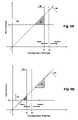
- the process space that is exploited by embodiments of the inventionmay be understood with reference to FIGS. 6A-6C .
- the process spacemay be characterized by relationships among the deposition and etch thicknesses.
- a traditional dep/etch/dep processis illustrated in FIG. 6A with the process spaced defined by the intersection of three regions in the etch-thickness-deposition-thickness plane.
- a traditional depositionis performed to provide a deposition thickness D 1 ⁇ D c , illustrated by the portion of the plane to the left of the vertical line at D 1 .
- the drawingnotes that the gap remains open for D 1 ⁇ D • , but closes when D 1 >D • .
- the traditional etchingis performed to remove an amount of material sufficient to reopen the gap a desired amount, illustrated by the portion of the plane above the horizontal line at E 1 .
- a third constraintmay be understood as follows, and imposes the condition that the etch be less than the amount that would reduce the open-field coverage to zero.
- the open field coverage T dep (open)is approximately proportion to the vertical deposition thickness D: T dep (open) ⁇ R dep D, where R dep is a positive real-number constant of proportionality.
- the blanket film etch amount E and the open-field etch amount T etch (open)are similarly approximately proportional: T etch (open) ⁇ R etch E, where R etch is also a positive real-number constant of proportionality.
- the process space for a traditional dep/etch/dep processis thus the region A in FIG. 6A representing the intersection of the areas defined by these three constraints.
- an increase in the aspect ratio and/or a decrease in the width of thecauses a decrease in the critical deposition thickness D c .
- FIG. 6Bwhere new, lower critical deposition thickness is denoted D c ′ and the corresponding initial deposition and etching thickness are respectively denoted D 1 ′ and E 1 ′.
- the resulting process space A′is smaller, and continues to grow ever smaller as applications are developed required deposition in higher-aspect-ratio narrower gaps. Region A is shown with stippled shading in FIG. 6A for comparison with region A′.
- FIG. 6Cillustrates the effect on process space when the constraint D 1 ⁇ D c is relaxed in accordance with embodiments of the invention (see block 512 of FIG. 5 ).
- the greater deposition thicknessis denoted D 1 ′′ and is greater than D c ′ (and therefore also greater than D 1 ′).
- the resulting process spaceis denoted A′′ and is larger than the process space A′ reproduced for purposes of comparison in FIG. 6C .
- process space A′′may define a region of processing conditions similar to or even larger than process space A, i.e. using processing conditions suitable for gaps having larger widths and/or smaller aspect ratios under a tradition approach.
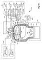
- FIG. 7Aschematically illustrates the structure of such an HDP-CVD system 710 in one embodiment.
- the system 710includes a chamber 713 , a vacuum system 770 , a source plasma system 780 A, a bias plasma system 780 B, a gas delivery system 733 , and a remote plasma cleaning system 750 .
- the upper portion of chamber 713includes a dome 714 , which is made of a ceramic dielectric material, such as aluminum oxide or aluminum nitride. Dome 714 defines an upper boundary of a plasma processing region 716 . Plasma processing region 716 is bounded on the bottom by the upper surface of a substrate 717 and a substrate support member 718 .
- a heater plate 723 and a cold plate 724surmount, and are thermally coupled to, dome 714 .
- Heater plate 723 and cold plate 724allow control of the dome temperature to within about ⁇ 10° C. over a range of about 100° C. to 200° C. This allows optimizing the dome temperature for the various processes. For example, it may be desirable to maintain the dome at a higher temperature for cleaning or etching processes than for deposition processes. Accurate control of the dome temperature also reduces the flake or particle counts in the chamber and improves adhesion between the deposited layer and the substrate.
- the lower portion of chamber 713includes a body member 722 , which joins the chamber to the vacuum system.
- a base portion 721 of substrate support member 718is mounted on, and forms a continuous inner surface with, body member 722 .
- Substratesare transferred into and out of chamber 713 by a robot blade (not shown) through an insertion/removal opening (not shown) in the side of chamber 713 .
- Lift pins(not shown) are raised and then lowered under the control of a motor (also not shown) to move the substrate from the robot blade at an upper loading position 757 to a lower processing position 756 in which the substrate is placed on a substrate receiving portion 719 of substrate support member 718 .
- Substrate receiving portion 719includes an electrostatic chuck 720 that secures the substrate to substrate support member 718 during substrate processing.
- substrate support member 718is made from an aluminum oxide or aluminum ceramic material.
- Vacuum system 770includes throttle body 725 , which houses twin-blade throttle valve 726 and is attached to gate valve 727 and turbo-molecular pump 728 . It should be noted that throttle body 725 offers minimum obstruction to gas flow, and allows symmetric pumping. Gate valve 727 can isolate pump 728 from throttle body 725 , and can also control chamber pressure by restricting the exhaust flow capacity when throttle valve 726 is fully open. The arrangement of the throttle valve, gate valve, and turbo-molecular pump allow accurate and stable control of chamber pressures up to about 1 millitorr to about 2 torr.
- the source plasma system 780 Aincludes a top coil 729 and side coil 730 , mounted on dome 714 .
- a symmetrical ground shield(not shown) reduces electrical coupling between the coils.
- Top coil 729is powered by top source RF (SRF) generator 731 A
- side coil 730is powered by side SRF generator 731 B, allowing independent power levels and frequencies of operation for each coil.
- SRFsource RF
- This dual coil systemallows control of the radial ion density in chamber 713 , thereby improving plasma uniformity.
- Side coil 730 and top coil 729are typically inductively driven, which does not require a complimentary electrode.
- the top source RF generator 731 Aprovides up to 2,500 watts of RF power at nominally 2 MHz and the side source RF generator 731 B provides up to 5,000 watts of RF power at nominally 2 MHz.
- the operating frequencies of the top and side RF generatorsmay be offset from the nominal operating frequency (e.g. to 1.7-1.9 MHz and 1.9-2.1 MHz, respectively) to improve plasma-generation efficiency.
- a bias plasma system 780 Bincludes a bias RF (“BRF”) generator 731 C and a bias matching network 732 C.
- the bias plasma system 780 Bcapacitively couples substrate portion 717 to body member 722 , which act as complimentary electrodes.
- the bias plasma system 780 Bserves to enhance the transport of plasma species (e.g., ions) created by the source plasma system 780 A to the surface of the substrate.
- bias RF generatorprovides up to 10,000 watts of RF power at a frequency less than 5 MHz, as discussed further below.
- RF generators 731 A and 731 Binclude digitally controlled synthesizers and operate over a frequency range between about 1.8 to about 2.1 MHz. Each generator includes an RF control circuit (not shown) that measures reflected power from the chamber and coil back to the generator and adjusts the frequency of operation to obtain the lowest reflected power, as understood by a person of ordinary skill in the art.
- RF generatorsare typically designed to operate into a load with a characteristic impedance of 50 ohms. RF power may be reflected from loads that have a different characteristic impedance than the generator. This can reduce power transferred to the load. Additionally, power reflected from the load back to the generator may overload and damage the generator.
- the impedance of a plasmamay range from less than 5 ohms to over 900 ohms, depending on the plasma ion density, among other factors, and because reflected power may be a function of frequency, adjusting the generator frequency according to the reflected power increases the power transferred from the RF generator to the plasma and protects the generator. Another way to reduce reflected power and improve efficiency is with a matching network.
- Matching networks 732 A and 732 Bmatch the output impedance of generators 731 A and 731 B with their respective coils 729 and 730 .
- the RF control circuitmay tune both matching networks by changing the value of capacitors within the matching networks to match the generator to the load as the load changes.
- the RF control circuitmay tune a matching network when the power reflected from the load back to the generator exceeds a certain limit.
- One way to provide a constant match, and effectively disable the RF control circuit from tuning the matching networkis to set the reflected power limit above any expected value of reflected power. This may help stabilize a plasma under some conditions by holding the matching network constant at its most recent condition.
- the RF control circuitcan be used to determine the power delivered to the load (plasma) and may increase or decrease the generator output power to keep the delivered power substantially constant during deposition of a layer.
- a gas delivery system 733provides gases from several sources, 734 A- 734 E chamber for processing the substrate via gas delivery lines 738 (only some of which are shown).
- gas delivery lines 738only some of which are shown.
- the actual sources used for sources 734 A- 734 E and the actual connection of delivery lines 738 to chamber 713varies depending on the deposition and cleaning processes executed within chamber 713 .
- Gasesare introduced into chamber 713 through a gas ring 737 and/or a top nozzle 745 .
- FIG. 7Bis a simplified, partial cross-sectional view of chamber 713 showing additional details of gas ring 737 .
- first and second gas sources, 734 A and 734 B, and first and second gas flow controllers, 735 A′ and 735 B′provide gas to ring plenum 736 in gas ring 737 via gas delivery lines 738 (only some of which are shown).
- Gas ring 737has a plurality of source gas nozzles 739 (only one of which is shown for purposes of illustration) that provide a uniform flow of gas over the substrate. Nozzle length and nozzle angle may be changed to allow tailoring of the uniformity profile and gas utilization efficiency for a particular process within an individual chamber.
- gas ring 737has 12 source gas nozzles made from an aluminum oxide ceramic.
- Gas ring 737also has a plurality of oxidizer gas nozzles 740 (only one of which is shown), which in a preferred embodiment are co-planar with and shorter than source gas nozzles 739 , and in one embodiment receive gas from body plenum 741 . In some embodiments it is desirable not to mix source gases and oxidizer gases before injecting the gases into chamber 713 . In other embodiments, oxidizer gas and source gas may be mixed prior to injecting the gases into chamber 713 by providing apertures (not shown) between body plenum 741 and gas ring plenum 736 .
- third, fourth, and fifth gas sources, 734 C, 734 D, and 734 D′, and third and fourth gas flow controllers, 735 C and 735 D′provide gas to body plenum via gas delivery lines 738 .
- Additional valves, such as 743 B (other valves not shown),may shut off gas from the flow controllers to the chamber.
- source 734 Acomprises a silane SiH 4 source
- source 734 Bcomprises a molecular oxygen O 2 source
- source 734 Ccomprises a silane SiH 4 source
- source 734 Dcomprises a helium He source
- source 734 D′comprises a molecular hydrogen H 2 source.
- valve 743 Bto isolate chamber 713 from delivery line 738 A and to vent delivery line 738 A to vacuum foreline 744 , for example.
- valve 743 A and 743 Cmay be incorporated on other gas delivery lines.
- Such three-way valvesmay be placed as close to chamber 713 as practical, to minimize the volume of the unvented gas delivery line (between the three-way valve and the chamber).
- two-way (on-off) valvesmay be placed between a mass flow controller (“MFC”) and the chamber or between a gas source and an MFC.
- MFCmass flow controller
- chamber 713also has top nozzle 745 and top vent 746 .
- Top nozzle 745 and top vent 746allow independent control of top and side flows of the gases, which improves film uniformity and allows fine adjustment of the film's deposition and doping parameters.
- Top vent 746is an annular opening around top nozzle 745 .
- first gas source 734 Asupplies source gas nozzles 739 and top nozzle 745 .
- Source nozzle MFC 735 A′controls the amount of gas delivered to source gas nozzles 739 and top nozzle MFC 735 A controls the amount of gas delivered to top gas nozzle 745 .
- two MFCs 735 B and 735 B′may be used to control the flow of oxygen to both top vent 746 and oxidizer gas nozzles 740 from a single source of oxygen, such as source 734 B.
- oxygenis not supplied to the chamber from any side nozzles.
- the gases supplied to top nozzle 745 and top vent 746may be kept separate prior to flowing the gases into chamber 713 , or the gases may be mixed in top plenum 748 before they flow into chamber 713 . Separate sources of the same gas may be used to supply various portions of the chamber.
- a remote microwave-generated plasma cleaning system 750is provided to periodically clean deposition residues from chamber components.
- the cleaning systemincludes a remote microwave generator 751 that creates a plasma from a cleaning gas source 734 E (e.g., molecular fluorine, nitrogen trifluoride, other fluorocarbons or equivalents) in reactor cavity 753 .
- the reactive species resulting from this plasmaare conveyed to chamber 713 through cleaning gas feed port 754 via applicator tube 755 .
- the materials used to contain the cleaning plasmae.g., cavity 753 and applicator tube 755 ) must be resistant to attack by the plasma.
- the distance between reactor cavity 753 and feed port 754should be kept as short as practical, since the concentration of desirable plasma species may decline with distance from reactor cavity 753 .
- Generating the cleaning plasma in a remote cavityallows the use of an efficient microwave generator and does not subject chamber components to the temperature, radiation, or bombardment of the glow discharge that may be present in a plasma formed in situ. Consequently, relatively sensitive components, such as electrostatic chuck 720 , do not need to be covered with a dummy wafer or otherwise protected, as may be required with an in situ plasma cleaning process.
- the plasma-cleaning system 750is shown disposed above the chamber 713 , although other positions may alternatively be used.
- a baffle 761may be provided proximate the top nozzle to direct flows of source gases supplied through the top nozzle into the chamber and to direct flows of remotely generated plasma.
- Source gases provided through top nozzle 745are directed through a central passage 762 into the chamber, while remotely generated plasma species provided through the cleaning gas feed port 754 are directed to the sides of the chamber 713 by the baffle 761 .
Landscapes
- Chemical & Material Sciences (AREA)
- General Chemical & Material Sciences (AREA)
- Chemical Kinetics & Catalysis (AREA)
- Engineering & Computer Science (AREA)
- Materials Engineering (AREA)
- Mechanical Engineering (AREA)
- Metallurgy (AREA)
- Organic Chemistry (AREA)
- Formation Of Insulating Films (AREA)
- Drying Of Semiconductors (AREA)
- Element Separation (AREA)
- Chemical Vapour Deposition (AREA)
Abstract
Description
The deposition/sputter ratio increases with increased deposition and decreases with increased sputtering. As used in the definition of D/S, the “net deposition rate” refers to the deposition rate that is measured when deposition and sputtering are occurring simultaneously. The “blanket sputter rate” is the sputter rate measured when the process recipe is run without deposition gases; the pressure within the process chamber is adjusted to the pressure during deposition and the sputter rate measured on a blanket thermal oxide.
which increases with increased sputtering and decreases with increased deposition. As used in the definition of E/D, the “net deposition rate” again refers to the deposition rate measured when deposition and sputtering are occurring simultaneously. The “source-only deposition rate,” however, refers to the deposition rate that is measured when the process recipe is run with no sputtering. Embodiments of the invention are described herein in terms of D/S ratios. While D/S and E/D are not precise reciprocals, they are inversely related and conversion between them will be understood to those of skill in the art.
Tdep(open)≅RdepD,
where Rdep isa positive real-number constant of proportionality. The blanket film etch amount E and the open-field etch amount Tetch(open)are similarly approximately proportional:
Tetch(open)≅RetchE,
where Retchis also a positive real-number constant of proportionality. The etching reduces the open-field coverage to zero when Tetch(open)=Tdep(open), i.e. when
In the graph, then, the constraint that the etch be less than the amount that would reduce the open-field coverage to zero is defined by that portion of the plane below the line having slope Rdep/Retch.
Claims (19)
Priority Applications (4)
| Application Number | Priority Date | Filing Date | Title |
|---|---|---|---|
| US11/166,357US7329586B2 (en) | 2005-06-24 | 2005-06-24 | Gapfill using deposition-etch sequence |
| JP2008518247AJP5225081B2 (en) | 2005-06-24 | 2006-06-15 | Gap filling using deposition and etching sequences |
| PCT/US2006/023311WO2007001878A2 (en) | 2005-06-24 | 2006-06-15 | Gapfill using deposition-etch sequence |
| CN2006800309381ACN101278380B (en) | 2005-06-24 | 2006-06-15 | Gap-fill processing using deposition-etch sequences |
Applications Claiming Priority (1)
| Application Number | Priority Date | Filing Date | Title |
|---|---|---|---|
| US11/166,357US7329586B2 (en) | 2005-06-24 | 2005-06-24 | Gapfill using deposition-etch sequence |
Publications (2)
| Publication Number | Publication Date |
|---|---|
| US20060292894A1 US20060292894A1 (en) | 2006-12-28 |
| US7329586B2true US7329586B2 (en) | 2008-02-12 |
Family
ID=37568134
Family Applications (1)
| Application Number | Title | Priority Date | Filing Date |
|---|---|---|---|
| US11/166,357Active2025-11-05US7329586B2 (en) | 2005-06-24 | 2005-06-24 | Gapfill using deposition-etch sequence |
Country Status (4)
| Country | Link |
|---|---|
| US (1) | US7329586B2 (en) |
| JP (1) | JP5225081B2 (en) |
| CN (1) | CN101278380B (en) |
| WO (1) | WO2007001878A2 (en) |
Cited By (3)
| Publication number | Priority date | Publication date | Assignee | Title |
|---|---|---|---|---|
| US20090064932A1 (en)* | 2007-08-31 | 2009-03-12 | Samsung Electronics Co., Ltd. | Apparatus for HDP-CVD and method of forming insulating layer using the same |
| US20090215214A1 (en)* | 2008-02-22 | 2009-08-27 | Mickael Renault | Method of Sealing a Cavity |
| US20090275163A1 (en)* | 2008-04-30 | 2009-11-05 | Joseph Damian Gordon Lacey | System and Method of Encapsulation |
Families Citing this family (25)
| Publication number | Priority date | Publication date | Assignee | Title |
|---|---|---|---|---|
| US7442620B2 (en)* | 2006-06-13 | 2008-10-28 | Macronix International Co., Ltd. | Methods for forming a trench isolation structure with rounded corners in a silicon substrate |
| US20080299775A1 (en)* | 2007-06-04 | 2008-12-04 | Applied Materials, Inc. | Gapfill extension of hdp-cvd integrated process modulation sio2 process |
| US7867921B2 (en)* | 2007-09-07 | 2011-01-11 | Applied Materials, Inc. | Reduction of etch-rate drift in HDP processes |
| US7745350B2 (en)* | 2007-09-07 | 2010-06-29 | Applied Materials, Inc. | Impurity control in HDP-CVD DEP/ETCH/DEP processes |
| US7972968B2 (en)* | 2008-08-18 | 2011-07-05 | Applied Materials, Inc. | High density plasma gapfill deposition-etch-deposition process etchant |
| JP5514420B2 (en)* | 2008-09-17 | 2014-06-04 | ルネサスエレクトロニクス株式会社 | Manufacturing method of semiconductor integrated circuit device |
| US7910491B2 (en)* | 2008-10-16 | 2011-03-22 | Applied Materials, Inc. | Gapfill improvement with low etch rate dielectric liners |
| JP5568244B2 (en)* | 2009-03-23 | 2014-08-06 | ラピスセミコンダクタ株式会社 | Manufacturing method of semiconductor device |
| US9257274B2 (en) | 2010-04-15 | 2016-02-09 | Lam Research Corporation | Gapfill of variable aspect ratio features with a composite PEALD and PECVD method |
| JP2012004542A (en)* | 2010-05-20 | 2012-01-05 | Tokyo Electron Ltd | Method and apparatus for forming silicon film |
| US8497211B2 (en) | 2011-06-24 | 2013-07-30 | Applied Materials, Inc. | Integrated process modulation for PSG gapfill |
| CN103681459B (en)* | 2012-09-05 | 2016-03-30 | 中芯国际集成电路制造(上海)有限公司 | Improve the method for before-metal medium layer gap-fill capabilities |
| US9087542B1 (en)* | 2012-12-10 | 2015-07-21 | Western Digital (Fremont), Llc | Method for providing a structure having reduced voids in a magnetic recording transducer |
| US9018108B2 (en) | 2013-01-25 | 2015-04-28 | Applied Materials, Inc. | Low shrinkage dielectric films |
| US20150206803A1 (en)* | 2014-01-19 | 2015-07-23 | United Microelectronics Corp. | Method of forming inter-level dielectric layer |
| US9425078B2 (en)* | 2014-02-26 | 2016-08-23 | Lam Research Corporation | Inhibitor plasma mediated atomic layer deposition for seamless feature fill |
| US9570289B2 (en)* | 2015-03-06 | 2017-02-14 | Lam Research Corporation | Method and apparatus to minimize seam effect during TEOS oxide film deposition |
| US9502238B2 (en) | 2015-04-03 | 2016-11-22 | Lam Research Corporation | Deposition of conformal films by atomic layer deposition and atomic layer etch |
| GB201620680D0 (en)* | 2016-12-05 | 2017-01-18 | Spts Technologies Ltd | Method of smoothing a surface |
| JP7203515B2 (en)* | 2017-06-06 | 2023-01-13 | アプライド マテリアルズ インコーポレイテッド | Bottom-up growth of silicon oxide and silicon nitride using a sequential deposition-etch-processing method |
| KR102726216B1 (en) | 2019-05-01 | 2024-11-04 | 램 리써치 코포레이션 | Modulated atomic layer deposition |
| US12408318B2 (en) | 2019-05-15 | 2025-09-02 | Micron Technology, Inc. | Semiconductor formation using hybrid oxidation |
| JP2022534793A (en) | 2019-06-07 | 2022-08-03 | ラム リサーチ コーポレーション | In situ control of film properties during atomic layer deposition |
| CN114207184A (en) | 2019-08-06 | 2022-03-18 | 朗姆研究公司 | Thermal Atomic Layer Deposition of Silicon-Containing Films |
| CN115735261A (en) | 2020-07-28 | 2023-03-03 | 朗姆研究公司 | Impurity reduction in silicon-containing films |
Citations (78)
| Publication number | Priority date | Publication date | Assignee | Title |
|---|---|---|---|---|
| US4468413A (en) | 1982-02-15 | 1984-08-28 | U.S. Philips Corporation | Method of manufacturing fluorine-doped optical fibers |
| JPS61276977A (en) | 1985-05-30 | 1986-12-06 | Canon Inc | Deposited film formation method |
| US4690746A (en) | 1986-02-24 | 1987-09-01 | Genus, Inc. | Interlayer dielectric process |
| US4851370A (en) | 1987-12-28 | 1989-07-25 | American Telephone And Telegraph Company, At&T Bell Laboratories | Fabricating a semiconductor device with low defect density oxide |
| US4872947A (en) | 1986-12-19 | 1989-10-10 | Applied Materials, Inc. | CVD of silicon oxide using TEOS decomposition and in-situ planarization process |
| US4892753A (en) | 1986-12-19 | 1990-01-09 | Applied Materials, Inc. | Process for PECVD of silicon oxide using TEOS decomposition |
| US4894352A (en) | 1988-10-26 | 1990-01-16 | Texas Instruments Inc. | Deposition of silicon-containing films using organosilicon compounds and nitrogen trifluoride |
| JPH0258836A (en) | 1988-08-24 | 1990-02-28 | Matsushita Electric Ind Co Ltd | Manufacturing method of semiconductor device |
| US4960488A (en) | 1986-12-19 | 1990-10-02 | Applied Materials, Inc. | Reactor chamber self-cleaning process |
| US5000113A (en) | 1986-12-19 | 1991-03-19 | Applied Materials, Inc. | Thermal CVD/PECVD reactor and use for thermal chemical vapor deposition of silicon dioxide and in-situ multi-step planarized process |
| US5013691A (en) | 1989-07-31 | 1991-05-07 | At&T Bell Laboratories | Anisotropic deposition of silicon dioxide |
| US5089442A (en) | 1990-09-20 | 1992-02-18 | At&T Bell Laboratories | Silicon dioxide deposition method using a magnetic field and both sputter deposition and plasma-enhanced cvd |
| JPH04239750A (en) | 1991-01-23 | 1992-08-27 | Nec Corp | Forming method for fluorine-containing silicon oxide film |
| US5156881A (en) | 1987-03-18 | 1992-10-20 | Kabushiki Kaisha Toshiba | Method for forming a film on a substrate by activating a reactive gas |
| WO1992020833A1 (en) | 1991-05-17 | 1992-11-26 | Lam Research Corporation | A PROCESS FOR DEPOSITING A SIOx FILM HAVING REDUCED INTRINSIC STRESS AND/OR REDUCED HYDROGEN CONTENT |
| JPH04341568A (en) | 1991-05-16 | 1992-11-27 | Toshiba Corp | Thin film forming method and thin film forming apparatus |
| US5271972A (en) | 1992-08-17 | 1993-12-21 | Applied Materials, Inc. | Method for depositing ozone/TEOS silicon oxide films of reduced surface sensitivity |
| US5275977A (en) | 1990-03-19 | 1994-01-04 | Hitachi, Ltd. | Insulating film forming method for semiconductor device interconnection |
| US5279865A (en) | 1991-06-28 | 1994-01-18 | Digital Equipment Corporation | High throughput interlevel dielectric gap filling process |
| US5288518A (en) | 1991-06-07 | 1994-02-22 | Nec Corproation | Chemical vapor deposition method for forming fluorine containing silicon oxide film |
| US5302233A (en) | 1993-03-19 | 1994-04-12 | Micron Semiconductor, Inc. | Method for shaping features of a semiconductor structure using chemical mechanical planarization (CMP) |
| US5314724A (en) | 1991-01-08 | 1994-05-24 | Fujitsu Limited | Process for forming silicon oxide film |
| US5319247A (en) | 1990-10-30 | 1994-06-07 | Mitsubishi Denki Kabushiki Kaisha | Semiconductor device having an interlayer insulating film of high crack resistance |
| US5334552A (en) | 1991-12-04 | 1994-08-02 | Nec Corporation | Method for fabricating a semiconductor device having a multi-layered interconnection structure |
| US5399529A (en) | 1992-05-27 | 1995-03-21 | Nec Corporation | Process for producing semiconductor devices |
| US5416048A (en) | 1993-04-16 | 1995-05-16 | Micron Semiconductor, Inc. | Method to slope conductor profile prior to dielectric deposition to improve dielectric step-coverage |
| US5420075A (en) | 1992-04-15 | 1995-05-30 | Nec Corporation | Forming multi-layered interconnections with fluorine compound treatment permitting selective deposition of insulator |
| JPH07161703A (en) | 1993-12-03 | 1995-06-23 | Ricoh Co Ltd | Method for manufacturing semiconductor device |
| US5429995A (en) | 1992-07-17 | 1995-07-04 | Kabushiki Kaisha Toshiba | Method of manufacturing silicon oxide film containing fluorine |
| US5468342A (en) | 1994-04-28 | 1995-11-21 | Cypress Semiconductor Corp. | Method of etching an oxide layer |
| US5474589A (en) | 1990-11-28 | 1995-12-12 | Sumitomo Electric Industries, Ltd. | UV light-permeable glass and article comprising the same |
| US5563105A (en) | 1994-09-30 | 1996-10-08 | International Business Machines Corporation | PECVD method of depositing fluorine doped oxide using a fluorine precursor containing a glass-forming element |
| US5571576A (en) | 1995-02-10 | 1996-11-05 | Watkins-Johnson | Method of forming a fluorinated silicon oxide layer using plasma chemical vapor deposition |
| US5599740A (en) | 1995-11-16 | 1997-02-04 | Taiwan Semiconductor Manufacturing Company, Ltd. | Deposit-etch-deposit ozone/teos insulator layer method |
| US5624582A (en) | 1993-01-21 | 1997-04-29 | Vlsi Technology, Inc. | Optimization of dry etching through the control of helium backside pressure |
| US5648175A (en) | 1996-02-14 | 1997-07-15 | Applied Materials, Inc. | Chemical vapor deposition reactor system and integrated circuit |
| US5661093A (en) | 1996-09-12 | 1997-08-26 | Applied Materials, Inc. | Method for the stabilization of halogen-doped films through the use of multiple sealing layers |
| US5679606A (en) | 1995-12-27 | 1997-10-21 | Taiwan Semiconductor Manufacturing Company, Ltd. | method of forming inter-metal-dielectric structure |
| US5719085A (en) | 1995-09-29 | 1998-02-17 | Intel Corporation | Shallow trench isolation technique |
| US5850105A (en) | 1997-03-21 | 1998-12-15 | Advanced Micro Devices, Inc. | Substantially planar semiconductor topography using dielectrics and chemical mechanical polish |
| US5858876A (en) | 1996-04-01 | 1999-01-12 | Chartered Semiconductor Manufacturing, Ltd. | Simultaneous deposit and etch method for forming a void-free and gap-filling insulator layer upon a patterned substrate layer |
| US5872052A (en) | 1996-02-12 | 1999-02-16 | Micron Technology, Inc. | Planarization using plasma oxidized amorphous silicon |
| US5872058A (en) | 1997-06-17 | 1999-02-16 | Novellus Systems, Inc. | High aspect ratio gapfill process by using HDP |
| US5913140A (en) | 1996-12-23 | 1999-06-15 | Lam Research Corporation | Method for reduction of plasma charging damage during chemical vapor deposition |
| US5915190A (en) | 1995-12-27 | 1999-06-22 | Lam Research Corporation | Methods for filling trenches in a semiconductor wafer |
| US5923993A (en)* | 1997-12-17 | 1999-07-13 | Advanced Micro Devices | Method for fabricating dishing free shallow isolation trenches |
| US5937323A (en) | 1997-06-03 | 1999-08-10 | Applied Materials, Inc. | Sequencing of the recipe steps for the optimal low-k HDP-CVD processing |
| US5939831A (en) | 1996-11-13 | 1999-08-17 | Applied Materials, Inc. | Methods and apparatus for pre-stabilized plasma generation for microwave clean applications |
| US5944902A (en) | 1997-02-10 | 1999-08-31 | Applied Materials, Inc. | Plasma source for HDP-CVD chamber |
| US5953635A (en) | 1996-12-19 | 1999-09-14 | Intel Corporation | Interlayer dielectric with a composite dielectric stack |
| US5968610A (en) | 1997-04-02 | 1999-10-19 | United Microelectronics Corp. | Multi-step high density plasma chemical vapor deposition process |
| US5990000A (en) | 1997-02-20 | 1999-11-23 | Applied Materials, Inc. | Method and apparatus for improving gap-fill capability using chemical and physical etchbacks |
| US6030881A (en) | 1998-05-05 | 2000-02-29 | Novellus Systems, Inc. | High throughput chemical vapor deposition process capable of filling high aspect ratio structures |
| US6037018A (en) | 1998-07-01 | 2000-03-14 | Taiwan Semiconductor Maufacturing Company | Shallow trench isolation filled by high density plasma chemical vapor deposition |
| US6039851A (en) | 1995-03-22 | 2000-03-21 | Micron Technology, Inc. | Reactive sputter faceting of silicon dioxide to enhance gap fill of spaces between metal lines |
| US6059643A (en) | 1997-02-21 | 2000-05-09 | Aplex, Inc. | Apparatus and method for polishing a flat surface using a belted polishing pad |
| US6136685A (en) | 1997-06-03 | 2000-10-24 | Applied Materials, Inc. | High deposition rate recipe for low dielectric constant films |
| US6170428B1 (en) | 1996-07-15 | 2001-01-09 | Applied Materials, Inc. | Symmetric tunable inductively coupled HDP-CVD reactor |
| US6189483B1 (en) | 1997-05-29 | 2001-02-20 | Applied Materials, Inc. | Process kit |
| US6191026B1 (en) | 1996-01-09 | 2001-02-20 | Applied Materials, Inc. | Method for submicron gap filling on a semiconductor substrate |
| US6194038B1 (en) | 1998-03-20 | 2001-02-27 | Applied Materials, Inc. | Method for deposition of a conformal layer on a substrate |
| US6197705B1 (en) | 1999-03-18 | 2001-03-06 | Chartered Semiconductor Manufacturing Ltd. | Method of silicon oxide and silicon glass films deposition |
| US6204200B1 (en) | 1997-05-05 | 2001-03-20 | Texas Instruments Incorporated | Process scheme to form controlled airgaps between interconnect lines to reduce capacitance |
| US6203863B1 (en) | 1998-11-27 | 2001-03-20 | United Microelectronics Corp. | Method of gap filling |
| US6265269B1 (en)* | 1999-08-04 | 2001-07-24 | Mosel Vitelic Inc. | Method for fabricating a concave bottom oxide in a trench |
| US6335261B1 (en)* | 2000-05-31 | 2002-01-01 | International Business Machines Corporation | Directional CVD process with optimized etchback |
| US6335288B1 (en) | 2000-08-24 | 2002-01-01 | Applied Materials, Inc. | Gas chemistry cycling to achieve high aspect ratio gapfill with HDP-CVD |
| US6395150B1 (en) | 1998-04-01 | 2002-05-28 | Novellus Systems, Inc. | Very high aspect ratio gapfill using HDP |
| US20020187655A1 (en) | 2001-05-11 | 2002-12-12 | Applied Materials, Inc. | HDP-CVD deposition process for filling high aspect ratio gaps |
| US6503843B1 (en) | 1999-09-21 | 2003-01-07 | Applied Materials, Inc. | Multistep chamber cleaning and film deposition process using a remote plasma that also enhances film gap fill |
| US6596654B1 (en) | 2001-08-24 | 2003-07-22 | Novellus Systems, Inc. | Gap fill for high aspect ratio structures |
| US20030207580A1 (en)* | 2002-05-03 | 2003-11-06 | Applied Materials, Inc. | HDP-CVD dep/etch/dep process for improved deposition into high aspect ratio features |
| US20040079728A1 (en)* | 2002-10-23 | 2004-04-29 | Applied Materials, Inc. | Reactive ion etching for semiconductor device feature topography modification |
| US6846745B1 (en)* | 2001-08-03 | 2005-01-25 | Novellus Systems, Inc. | High-density plasma process for filling high aspect ratio structures |
| US6867086B1 (en)* | 2003-03-13 | 2005-03-15 | Novellus Systems, Inc. | Multi-step deposition and etch back gap fill process |
| US7078312B1 (en)* | 2003-09-02 | 2006-07-18 | Novellus Systems, Inc. | Method for controlling etch process repeatability |
| US7163896B1 (en)* | 2003-12-10 | 2007-01-16 | Novellus Systems, Inc. | Biased H2 etch process in deposition-etch-deposition gap fill |
| US7205240B2 (en)* | 2003-06-04 | 2007-04-17 | Applied Materials, Inc. | HDP-CVD multistep gapfill process |
Family Cites Families (4)
| Publication number | Priority date | Publication date | Assignee | Title |
|---|---|---|---|---|
| US5416046A (en)* | 1994-01-18 | 1995-05-16 | Wang; Ping-Lung | Method for making semiconductor heat-cooling device having a supporting mesh |
| KR100319185B1 (en)* | 1998-07-31 | 2002-01-04 | 윤종용 | Method for forming dielectric layer |
| KR100403630B1 (en)* | 2001-07-07 | 2003-10-30 | 삼성전자주식회사 | Method for forming inter-layer dielectric film of semiconductor device by HDP CVD |
| JP3975099B2 (en)* | 2002-03-26 | 2007-09-12 | 富士通株式会社 | Manufacturing method of semiconductor device |
- 2005
- 2005-06-24USUS11/166,357patent/US7329586B2/enactiveActive
- 2006
- 2006-06-15CNCN2006800309381Apatent/CN101278380B/ennot_activeExpired - Fee Related
- 2006-06-15WOPCT/US2006/023311patent/WO2007001878A2/ennot_activeCeased
- 2006-06-15JPJP2008518247Apatent/JP5225081B2/enactiveActive
Patent Citations (84)
| Publication number | Priority date | Publication date | Assignee | Title |
|---|---|---|---|---|
| US4468413A (en) | 1982-02-15 | 1984-08-28 | U.S. Philips Corporation | Method of manufacturing fluorine-doped optical fibers |
| JPS61276977A (en) | 1985-05-30 | 1986-12-06 | Canon Inc | Deposited film formation method |
| US4690746A (en) | 1986-02-24 | 1987-09-01 | Genus, Inc. | Interlayer dielectric process |
| US4872947A (en) | 1986-12-19 | 1989-10-10 | Applied Materials, Inc. | CVD of silicon oxide using TEOS decomposition and in-situ planarization process |
| US4892753A (en) | 1986-12-19 | 1990-01-09 | Applied Materials, Inc. | Process for PECVD of silicon oxide using TEOS decomposition |
| US5362526A (en) | 1986-12-19 | 1994-11-08 | Applied Materials, Inc. | Plasma-enhanced CVD process using TEOS for depositing silicon oxide |
| US4960488A (en) | 1986-12-19 | 1990-10-02 | Applied Materials, Inc. | Reactor chamber self-cleaning process |
| US5000113A (en) | 1986-12-19 | 1991-03-19 | Applied Materials, Inc. | Thermal CVD/PECVD reactor and use for thermal chemical vapor deposition of silicon dioxide and in-situ multi-step planarized process |
| US6167834B1 (en) | 1986-12-19 | 2001-01-02 | Applied Materials, Inc. | Thermal CVD/PECVD reactor and use for thermal chemical vapor deposition of silicon dioxide and in-situ multi-step planarized process |
| US5385763A (en) | 1987-03-18 | 1995-01-31 | Kabushiki Kaisha Toshiba | Method for forming a film on a substrate by activating a reactive gas |
| US5156881A (en) | 1987-03-18 | 1992-10-20 | Kabushiki Kaisha Toshiba | Method for forming a film on a substrate by activating a reactive gas |
| US4851370A (en) | 1987-12-28 | 1989-07-25 | American Telephone And Telegraph Company, At&T Bell Laboratories | Fabricating a semiconductor device with low defect density oxide |
| JPH0258836A (en) | 1988-08-24 | 1990-02-28 | Matsushita Electric Ind Co Ltd | Manufacturing method of semiconductor device |
| US4894352A (en) | 1988-10-26 | 1990-01-16 | Texas Instruments Inc. | Deposition of silicon-containing films using organosilicon compounds and nitrogen trifluoride |
| US5013691A (en) | 1989-07-31 | 1991-05-07 | At&T Bell Laboratories | Anisotropic deposition of silicon dioxide |
| US5275977A (en) | 1990-03-19 | 1994-01-04 | Hitachi, Ltd. | Insulating film forming method for semiconductor device interconnection |
| US5089442A (en) | 1990-09-20 | 1992-02-18 | At&T Bell Laboratories | Silicon dioxide deposition method using a magnetic field and both sputter deposition and plasma-enhanced cvd |
| US5319247A (en) | 1990-10-30 | 1994-06-07 | Mitsubishi Denki Kabushiki Kaisha | Semiconductor device having an interlayer insulating film of high crack resistance |
| US5474589A (en) | 1990-11-28 | 1995-12-12 | Sumitomo Electric Industries, Ltd. | UV light-permeable glass and article comprising the same |
| US5314724A (en) | 1991-01-08 | 1994-05-24 | Fujitsu Limited | Process for forming silicon oxide film |
| US5215787A (en) | 1991-01-23 | 1993-06-01 | Nec Corporation | Method of forming silicon oxide film containing fluorine |
| JPH04239750A (en) | 1991-01-23 | 1992-08-27 | Nec Corp | Forming method for fluorine-containing silicon oxide film |
| JPH04341568A (en) | 1991-05-16 | 1992-11-27 | Toshiba Corp | Thin film forming method and thin film forming apparatus |
| US5413967A (en) | 1991-05-16 | 1995-05-09 | Kabushiki Kaisha Toshiba | Method of manufacturing semiconductor devices |
| WO1992020833A1 (en) | 1991-05-17 | 1992-11-26 | Lam Research Corporation | A PROCESS FOR DEPOSITING A SIOx FILM HAVING REDUCED INTRINSIC STRESS AND/OR REDUCED HYDROGEN CONTENT |
| US5288518A (en) | 1991-06-07 | 1994-02-22 | Nec Corproation | Chemical vapor deposition method for forming fluorine containing silicon oxide film |
| US5279865A (en) | 1991-06-28 | 1994-01-18 | Digital Equipment Corporation | High throughput interlevel dielectric gap filling process |
| US5334552A (en) | 1991-12-04 | 1994-08-02 | Nec Corporation | Method for fabricating a semiconductor device having a multi-layered interconnection structure |
| US5420075A (en) | 1992-04-15 | 1995-05-30 | Nec Corporation | Forming multi-layered interconnections with fluorine compound treatment permitting selective deposition of insulator |
| US5399529A (en) | 1992-05-27 | 1995-03-21 | Nec Corporation | Process for producing semiconductor devices |
| US5429995A (en) | 1992-07-17 | 1995-07-04 | Kabushiki Kaisha Toshiba | Method of manufacturing silicon oxide film containing fluorine |
| US5271972A (en) | 1992-08-17 | 1993-12-21 | Applied Materials, Inc. | Method for depositing ozone/TEOS silicon oxide films of reduced surface sensitivity |
| US5624582A (en) | 1993-01-21 | 1997-04-29 | Vlsi Technology, Inc. | Optimization of dry etching through the control of helium backside pressure |
| US5302233A (en) | 1993-03-19 | 1994-04-12 | Micron Semiconductor, Inc. | Method for shaping features of a semiconductor structure using chemical mechanical planarization (CMP) |
| US5416048A (en) | 1993-04-16 | 1995-05-16 | Micron Semiconductor, Inc. | Method to slope conductor profile prior to dielectric deposition to improve dielectric step-coverage |
| JPH07161703A (en) | 1993-12-03 | 1995-06-23 | Ricoh Co Ltd | Method for manufacturing semiconductor device |
| US5468342A (en) | 1994-04-28 | 1995-11-21 | Cypress Semiconductor Corp. | Method of etching an oxide layer |
| US5563105A (en) | 1994-09-30 | 1996-10-08 | International Business Machines Corporation | PECVD method of depositing fluorine doped oxide using a fluorine precursor containing a glass-forming element |
| US5571576A (en) | 1995-02-10 | 1996-11-05 | Watkins-Johnson | Method of forming a fluorinated silicon oxide layer using plasma chemical vapor deposition |
| US6039851A (en) | 1995-03-22 | 2000-03-21 | Micron Technology, Inc. | Reactive sputter faceting of silicon dioxide to enhance gap fill of spaces between metal lines |
| US5719085A (en) | 1995-09-29 | 1998-02-17 | Intel Corporation | Shallow trench isolation technique |
| US5599740A (en) | 1995-11-16 | 1997-02-04 | Taiwan Semiconductor Manufacturing Company, Ltd. | Deposit-etch-deposit ozone/teos insulator layer method |
| US5679606A (en) | 1995-12-27 | 1997-10-21 | Taiwan Semiconductor Manufacturing Company, Ltd. | method of forming inter-metal-dielectric structure |
| US5915190A (en) | 1995-12-27 | 1999-06-22 | Lam Research Corporation | Methods for filling trenches in a semiconductor wafer |
| US6191026B1 (en) | 1996-01-09 | 2001-02-20 | Applied Materials, Inc. | Method for submicron gap filling on a semiconductor substrate |
| US5872052A (en) | 1996-02-12 | 1999-02-16 | Micron Technology, Inc. | Planarization using plasma oxidized amorphous silicon |
| US5648175A (en) | 1996-02-14 | 1997-07-15 | Applied Materials, Inc. | Chemical vapor deposition reactor system and integrated circuit |
| US5858876A (en) | 1996-04-01 | 1999-01-12 | Chartered Semiconductor Manufacturing, Ltd. | Simultaneous deposit and etch method for forming a void-free and gap-filling insulator layer upon a patterned substrate layer |
| US6182602B1 (en) | 1996-07-15 | 2001-02-06 | Applied Materials, Inc. | Inductively coupled HDP-CVD reactor |
| US6170428B1 (en) | 1996-07-15 | 2001-01-09 | Applied Materials, Inc. | Symmetric tunable inductively coupled HDP-CVD reactor |
| US5661093A (en) | 1996-09-12 | 1997-08-26 | Applied Materials, Inc. | Method for the stabilization of halogen-doped films through the use of multiple sealing layers |
| US5939831A (en) | 1996-11-13 | 1999-08-17 | Applied Materials, Inc. | Methods and apparatus for pre-stabilized plasma generation for microwave clean applications |
| US5953635A (en) | 1996-12-19 | 1999-09-14 | Intel Corporation | Interlayer dielectric with a composite dielectric stack |
| US5913140A (en) | 1996-12-23 | 1999-06-15 | Lam Research Corporation | Method for reduction of plasma charging damage during chemical vapor deposition |
| US5944902A (en) | 1997-02-10 | 1999-08-31 | Applied Materials, Inc. | Plasma source for HDP-CVD chamber |
| US5990000A (en) | 1997-02-20 | 1999-11-23 | Applied Materials, Inc. | Method and apparatus for improving gap-fill capability using chemical and physical etchbacks |
| US6059643A (en) | 1997-02-21 | 2000-05-09 | Aplex, Inc. | Apparatus and method for polishing a flat surface using a belted polishing pad |
| US5850105A (en) | 1997-03-21 | 1998-12-15 | Advanced Micro Devices, Inc. | Substantially planar semiconductor topography using dielectrics and chemical mechanical polish |
| US5968610A (en) | 1997-04-02 | 1999-10-19 | United Microelectronics Corp. | Multi-step high density plasma chemical vapor deposition process |
| US6204200B1 (en) | 1997-05-05 | 2001-03-20 | Texas Instruments Incorporated | Process scheme to form controlled airgaps between interconnect lines to reduce capacitance |
| US6189483B1 (en) | 1997-05-29 | 2001-02-20 | Applied Materials, Inc. | Process kit |
| US6136685A (en) | 1997-06-03 | 2000-10-24 | Applied Materials, Inc. | High deposition rate recipe for low dielectric constant films |
| US5937323A (en) | 1997-06-03 | 1999-08-10 | Applied Materials, Inc. | Sequencing of the recipe steps for the optimal low-k HDP-CVD processing |
| US5872058A (en) | 1997-06-17 | 1999-02-16 | Novellus Systems, Inc. | High aspect ratio gapfill process by using HDP |
| US5923993A (en)* | 1997-12-17 | 1999-07-13 | Advanced Micro Devices | Method for fabricating dishing free shallow isolation trenches |
| US6194038B1 (en) | 1998-03-20 | 2001-02-27 | Applied Materials, Inc. | Method for deposition of a conformal layer on a substrate |
| US6395150B1 (en) | 1998-04-01 | 2002-05-28 | Novellus Systems, Inc. | Very high aspect ratio gapfill using HDP |
| US6030881A (en) | 1998-05-05 | 2000-02-29 | Novellus Systems, Inc. | High throughput chemical vapor deposition process capable of filling high aspect ratio structures |
| US6037018A (en) | 1998-07-01 | 2000-03-14 | Taiwan Semiconductor Maufacturing Company | Shallow trench isolation filled by high density plasma chemical vapor deposition |
| US6203863B1 (en) | 1998-11-27 | 2001-03-20 | United Microelectronics Corp. | Method of gap filling |
| US6197705B1 (en) | 1999-03-18 | 2001-03-06 | Chartered Semiconductor Manufacturing Ltd. | Method of silicon oxide and silicon glass films deposition |
| US6265269B1 (en)* | 1999-08-04 | 2001-07-24 | Mosel Vitelic Inc. | Method for fabricating a concave bottom oxide in a trench |
| US6503843B1 (en) | 1999-09-21 | 2003-01-07 | Applied Materials, Inc. | Multistep chamber cleaning and film deposition process using a remote plasma that also enhances film gap fill |
| US6335261B1 (en)* | 2000-05-31 | 2002-01-01 | International Business Machines Corporation | Directional CVD process with optimized etchback |
| US6335288B1 (en) | 2000-08-24 | 2002-01-01 | Applied Materials, Inc. | Gas chemistry cycling to achieve high aspect ratio gapfill with HDP-CVD |
| US20020187655A1 (en) | 2001-05-11 | 2002-12-12 | Applied Materials, Inc. | HDP-CVD deposition process for filling high aspect ratio gaps |
| US6846745B1 (en)* | 2001-08-03 | 2005-01-25 | Novellus Systems, Inc. | High-density plasma process for filling high aspect ratio structures |
| US6596654B1 (en) | 2001-08-24 | 2003-07-22 | Novellus Systems, Inc. | Gap fill for high aspect ratio structures |
| US20030207580A1 (en)* | 2002-05-03 | 2003-11-06 | Applied Materials, Inc. | HDP-CVD dep/etch/dep process for improved deposition into high aspect ratio features |
| US20040079728A1 (en)* | 2002-10-23 | 2004-04-29 | Applied Materials, Inc. | Reactive ion etching for semiconductor device feature topography modification |
| US6867086B1 (en)* | 2003-03-13 | 2005-03-15 | Novellus Systems, Inc. | Multi-step deposition and etch back gap fill process |
| US7205240B2 (en)* | 2003-06-04 | 2007-04-17 | Applied Materials, Inc. | HDP-CVD multistep gapfill process |
| US7078312B1 (en)* | 2003-09-02 | 2006-07-18 | Novellus Systems, Inc. | Method for controlling etch process repeatability |
| US7163896B1 (en)* | 2003-12-10 | 2007-01-16 | Novellus Systems, Inc. | Biased H2 etch process in deposition-etch-deposition gap fill |
Non-Patent Citations (16)
Cited By (6)
| Publication number | Priority date | Publication date | Assignee | Title |
|---|---|---|---|---|
| US20090064932A1 (en)* | 2007-08-31 | 2009-03-12 | Samsung Electronics Co., Ltd. | Apparatus for HDP-CVD and method of forming insulating layer using the same |
| US20090215214A1 (en)* | 2008-02-22 | 2009-08-27 | Mickael Renault | Method of Sealing a Cavity |
| US7989262B2 (en) | 2008-02-22 | 2011-08-02 | Cavendish Kinetics, Ltd. | Method of sealing a cavity |
| US8395249B2 (en) | 2008-02-22 | 2013-03-12 | Cavendish Kinetics, Ltd. | Sealed cavity |
| US20090275163A1 (en)* | 2008-04-30 | 2009-11-05 | Joseph Damian Gordon Lacey | System and Method of Encapsulation |
| US7993950B2 (en) | 2008-04-30 | 2011-08-09 | Cavendish Kinetics, Ltd. | System and method of encapsulation |
Also Published As
| Publication number | Publication date |
|---|---|
| CN101278380A (en) | 2008-10-01 |
| JP2008547224A (en) | 2008-12-25 |
| JP5225081B2 (en) | 2013-07-03 |
| US20060292894A1 (en) | 2006-12-28 |
| CN101278380B (en) | 2012-05-23 |
| WO2007001878A3 (en) | 2007-08-09 |
| WO2007001878A2 (en) | 2007-01-04 |
Similar Documents
| Publication | Publication Date | Title |
|---|---|---|
| US7329586B2 (en) | Gapfill using deposition-etch sequence | |
| US8414747B2 (en) | High-throughput HDP-CVD processes for advanced gapfill applications | |
| US7867921B2 (en) | Reduction of etch-rate drift in HDP processes | |
| US7097886B2 (en) | Deposition process for high aspect ratio trenches | |
| US6808748B2 (en) | Hydrogen assisted HDP-CVD deposition process for aggressive gap-fill technology | |
| US7244658B2 (en) | Low stress STI films and methods | |
| US20140187045A1 (en) | Silicon nitride gapfill implementing high density plasma | |
| US7745350B2 (en) | Impurity control in HDP-CVD DEP/ETCH/DEP processes | |
| WO2006074489A1 (en) | Low-frequency bias power in hdp-cvd processes | |
| US20070029046A1 (en) | Methods and systems for increasing substrate temperature in plasma reactors | |
| CN101414551B (en) | Reduction of etch-rate drift in hdp processes | |
| US7229931B2 (en) | Oxygen plasma treatment for enhanced HDP-CVD gapfill | |
| US7189639B2 (en) | Use of germanium dioxide and/or alloys of GeO2 with silicon dioxide for semiconductor dielectric applications | |
| US8497211B2 (en) | Integrated process modulation for PSG gapfill | |
| US20080299775A1 (en) | Gapfill extension of hdp-cvd integrated process modulation sio2 process | |
| US20070111543A1 (en) | Methods for improving low k FSG film gap-fill characteristics | |
| US20050260356A1 (en) | Microcontamination abatement in semiconductor processing |
Legal Events
| Date | Code | Title | Description |
|---|---|---|---|
| AS | Assignment | Owner name:APPLIED MATERIALS, INC., CALIFORNIA Free format text:ASSIGNMENT OF ASSIGNORS INTEREST;ASSIGNORS:VELLAIKAL, MANOJ;MUNGEKAR, HEMANT P.;LEE, YOUNG S.;AND OTHERS;REEL/FRAME:017260/0104;SIGNING DATES FROM 20060130 TO 20060220 Owner name:MATSUSHITA ELECTRIC INDUSTRIAL CO., LTD., JAPAN Free format text:ASSIGNMENT OF ASSIGNORS INTEREST;ASSIGNORS:VELLAIKAL, MANOJ;MUNGEKAR, HEMANT P.;LEE, YOUNG S.;AND OTHERS;REEL/FRAME:017260/0104;SIGNING DATES FROM 20060130 TO 20060220 | |
| STCF | Information on status: patent grant | Free format text:PATENTED CASE | |
| FPAY | Fee payment | Year of fee payment:4 | |
| FPAY | Fee payment | Year of fee payment:8 | |
| MAFP | Maintenance fee payment | Free format text:PAYMENT OF MAINTENANCE FEE, 12TH YEAR, LARGE ENTITY (ORIGINAL EVENT CODE: M1553); ENTITY STATUS OF PATENT OWNER: LARGE ENTITY Year of fee payment:12 | |
| AS | Assignment | Owner name:PANASONIC CORPORATION, JAPAN Free format text:CHANGE OF NAME;ASSIGNOR:MATSUSHITA ELECTRIC INDUSTRIAL CO., LTD.;REEL/FRAME:052184/0943 Effective date:20081001 | |
| AS | Assignment | Owner name:NUVOTON TECHNOLOGY CORPORATION JAPAN, JAPAN Free format text:ASSIGNMENT OF ASSIGNORS INTEREST;ASSIGNOR:PANASONIC CORPORATION;REEL/FRAME:055502/0185 Effective date:20200901 |