US7327510B2 - Process for modifying offset voltage characteristics of an interferometric modulator - Google Patents
Process for modifying offset voltage characteristics of an interferometric modulatorDownload PDFInfo
- Publication number
- US7327510B2 US7327510B2US11/208,052US20805205AUS7327510B2US 7327510 B2US7327510 B2US 7327510B2US 20805205 AUS20805205 AUS 20805205AUS 7327510 B2US7327510 B2US 7327510B2
- Authority
- US
- United States
- Prior art keywords
- interferometric modulator
- processing parameters
- modifying
- offset voltage
- zero
- Prior art date
- Legal status (The legal status is an assumption and is not a legal conclusion. Google has not performed a legal analysis and makes no representation as to the accuracy of the status listed.)
- Expired - Fee Related, expires
Links
- 238000000034methodMethods0.000titleclaimsabstractdescription132
- 230000008569processEffects0.000titleclaimsabstractdescription59
- 238000012545processingMethods0.000claimsabstractdescription100
- 238000004519manufacturing processMethods0.000claimsabstractdescription57
- 230000008021depositionEffects0.000claimsabstractdescription40
- 238000000137annealingMethods0.000claimsabstractdescription20
- 230000003287optical effectEffects0.000claimsdescription38
- 238000011165process developmentMethods0.000claimsdescription26
- 239000000758substrateSubstances0.000claimsdescription13
- 238000010438heat treatmentMethods0.000claimsdescription12
- 150000002500ionsChemical class0.000claimsdescription5
- 230000000284resting effectEffects0.000claimsdescription2
- 238000004891communicationMethods0.000claims2
- 238000000151depositionMethods0.000description41
- 239000000463materialSubstances0.000description26
- 238000010586diagramMethods0.000description15
- 238000005530etchingMethods0.000description15
- 230000015572biosynthetic processEffects0.000description14
- 238000000623plasma-assisted chemical vapour depositionMethods0.000description14
- 238000004140cleaningMethods0.000description9
- 238000013461designMethods0.000description9
- 238000002230thermal chemical vapour depositionMethods0.000description9
- 238000005094computer simulationMethods0.000description8
- 229910052751metalInorganic materials0.000description7
- 239000002184metalSubstances0.000description7
- 238000000059patterningMethods0.000description7
- 238000004528spin coatingMethods0.000description7
- 238000001816coolingMethods0.000description6
- 238000005240physical vapour depositionMethods0.000description6
- 238000012360testing methodMethods0.000description6
- 230000003750conditioning effectEffects0.000description5
- 239000007789gasSubstances0.000description5
- BLIQUJLAJXRXSG-UHFFFAOYSA-N1-benzyl-3-(trifluoromethyl)pyrrolidin-1-ium-3-carboxylateChemical compoundC1C(C(=O)O)(C(F)(F)F)CCN1CC1=CC=CC=C1BLIQUJLAJXRXSG-UHFFFAOYSA-N0.000description4
- 230000008901benefitEffects0.000description4
- 230000008859changeEffects0.000description4
- 238000003050experimental design methodMethods0.000description4
- 239000003990capacitorSubstances0.000description3
- 230000001413cellular effectEffects0.000description3
- 230000033001locomotionEffects0.000description3
- 230000000873masking effectEffects0.000description3
- 239000004033plasticSubstances0.000description3
- 239000000126substanceSubstances0.000description3
- VYZAMTAEIAYCRO-UHFFFAOYSA-NChromiumChemical compound[Cr]VYZAMTAEIAYCRO-UHFFFAOYSA-N0.000description2
- ZOKXTWBITQBERF-UHFFFAOYSA-NMolybdenumChemical compound[Mo]ZOKXTWBITQBERF-UHFFFAOYSA-N0.000description2
- 229910052782aluminiumInorganic materials0.000description2
- XAGFODPZIPBFFR-UHFFFAOYSA-NaluminiumChemical compound[Al]XAGFODPZIPBFFR-UHFFFAOYSA-N0.000description2
- 229910021417amorphous siliconInorganic materials0.000description2
- 238000003491arrayMethods0.000description2
- 229910052804chromiumInorganic materials0.000description2
- 239000011651chromiumSubstances0.000description2
- 230000000694effectsEffects0.000description2
- 238000005516engineering processMethods0.000description2
- 239000011521glassSubstances0.000description2
- 238000010348incorporationMethods0.000description2
- AMGQUBHHOARCQH-UHFFFAOYSA-Nindium;oxotinChemical compound[In].[Sn]=OAMGQUBHHOARCQH-UHFFFAOYSA-N0.000description2
- 239000012528membraneSubstances0.000description2
- 238000012986modificationMethods0.000description2
- 230000004048modificationEffects0.000description2
- 229910052750molybdenumInorganic materials0.000description2
- 239000011733molybdenumSubstances0.000description2
- 238000006386neutralization reactionMethods0.000description2
- 238000005498polishingMethods0.000description2
- 230000002040relaxant effectEffects0.000description2
- 230000008439repair processEffects0.000description2
- 238000004544sputter depositionMethods0.000description2
- 230000000007visual effectEffects0.000description2
- IRLPACMLTUPBCL-KQYNXXCUSA-N5'-adenylyl sulfateChemical compoundC1=NC=2C(N)=NC=NC=2N1[C@@H]1O[C@H](COP(O)(=O)OS(O)(=O)=O)[C@@H](O)[C@H]1OIRLPACMLTUPBCL-KQYNXXCUSA-N0.000description1
- 238000012935AveragingMethods0.000description1
- UFHFLCQGNIYNRP-UHFFFAOYSA-NHydrogenChemical compound[H][H]UFHFLCQGNIYNRP-UHFFFAOYSA-N0.000description1
- HBBGRARXTFLTSG-UHFFFAOYSA-NLithium ionChemical compound[Li+]HBBGRARXTFLTSG-UHFFFAOYSA-N0.000description1
- 238000009825accumulationMethods0.000description1
- 238000004458analytical methodMethods0.000description1
- 238000009638autodisplayMethods0.000description1
- 230000009286beneficial effectEffects0.000description1
- 230000005540biological transmissionEffects0.000description1
- OJIJEKBXJYRIBZ-UHFFFAOYSA-Ncadmium nickelChemical compound[Ni].[Cd]OJIJEKBXJYRIBZ-UHFFFAOYSA-N0.000description1
- 239000000919ceramicSubstances0.000description1
- 238000007600chargingMethods0.000description1
- 238000003486chemical etchingMethods0.000description1
- 238000005229chemical vapour depositionMethods0.000description1
- 239000003086colorantSubstances0.000description1
- 239000004020conductorSubstances0.000description1
- 230000003247decreasing effectEffects0.000description1
- 239000003989dielectric materialSubstances0.000description1
- 238000004146energy storageMethods0.000description1
- 230000001747exhibiting effectEffects0.000description1
- 238000002474experimental methodMethods0.000description1
- 238000011049fillingMethods0.000description1
- 239000001257hydrogenSubstances0.000description1
- 229910052739hydrogenInorganic materials0.000description1
- 238000001746injection mouldingMethods0.000description1
- 230000010354integrationEffects0.000description1
- 238000005468ion implantationMethods0.000description1
- 230000000670limiting effectEffects0.000description1
- 229910001416lithium ionInorganic materials0.000description1
- 239000011159matrix materialSubstances0.000description1
- 238000005259measurementMethods0.000description1
- 239000007769metal materialSubstances0.000description1
- 238000005459micromachiningMethods0.000description1
- 238000013508migrationMethods0.000description1
- 230000005012migrationEffects0.000description1
- 238000005457optimizationMethods0.000description1
- 238000004806packaging method and processMethods0.000description1
- 239000003973paintSubstances0.000description1
- 238000001020plasma etchingMethods0.000description1
- 229920000642polymerPolymers0.000description1
- 238000002360preparation methodMethods0.000description1
- 238000003908quality control methodMethods0.000description1
- 230000002829reductive effectEffects0.000description1
- 239000005060rubberSubstances0.000description1
- 238000005070samplingMethods0.000description1
- 239000004065semiconductorSubstances0.000description1
- 238000000926separation methodMethods0.000description1
- 238000003860storageMethods0.000description1
- 238000006467substitution reactionMethods0.000description1
- 238000012546transferMethods0.000description1
- 238000007666vacuum formingMethods0.000description1
- 238000005406washingMethods0.000description1
- 238000001039wet etchingMethods0.000description1
- 210000000707wristAnatomy0.000description1
Images


Classifications
- G—PHYSICS
- G09—EDUCATION; CRYPTOGRAPHY; DISPLAY; ADVERTISING; SEALS
- G09G—ARRANGEMENTS OR CIRCUITS FOR CONTROL OF INDICATING DEVICES USING STATIC MEANS TO PRESENT VARIABLE INFORMATION
- G09G3/00—Control arrangements or circuits, of interest only in connection with visual indicators other than cathode-ray tubes
- G09G3/20—Control arrangements or circuits, of interest only in connection with visual indicators other than cathode-ray tubes for presentation of an assembly of a number of characters, e.g. a page, by composing the assembly by combination of individual elements arranged in a matrix no fixed position being assigned to or needed to be assigned to the individual characters or partial characters
- G09G3/34—Control arrangements or circuits, of interest only in connection with visual indicators other than cathode-ray tubes for presentation of an assembly of a number of characters, e.g. a page, by composing the assembly by combination of individual elements arranged in a matrix no fixed position being assigned to or needed to be assigned to the individual characters or partial characters by control of light from an independent source
- G09G3/3433—Control arrangements or circuits, of interest only in connection with visual indicators other than cathode-ray tubes for presentation of an assembly of a number of characters, e.g. a page, by composing the assembly by combination of individual elements arranged in a matrix no fixed position being assigned to or needed to be assigned to the individual characters or partial characters by control of light from an independent source using light modulating elements actuated by an electric field and being other than liquid crystal devices and electrochromic devices
- G09G3/3466—Control arrangements or circuits, of interest only in connection with visual indicators other than cathode-ray tubes for presentation of an assembly of a number of characters, e.g. a page, by composing the assembly by combination of individual elements arranged in a matrix no fixed position being assigned to or needed to be assigned to the individual characters or partial characters by control of light from an independent source using light modulating elements actuated by an electric field and being other than liquid crystal devices and electrochromic devices based on interferometric effect
- G—PHYSICS
- G02—OPTICS
- G02B—OPTICAL ELEMENTS, SYSTEMS OR APPARATUS
- G02B26/00—Optical devices or arrangements for the control of light using movable or deformable optical elements
- G02B26/001—Optical devices or arrangements for the control of light using movable or deformable optical elements based on interference in an adjustable optical cavity
- G—PHYSICS
- G09—EDUCATION; CRYPTOGRAPHY; DISPLAY; ADVERTISING; SEALS
- G09G—ARRANGEMENTS OR CIRCUITS FOR CONTROL OF INDICATING DEVICES USING STATIC MEANS TO PRESENT VARIABLE INFORMATION
- G09G2320/00—Control of display operating conditions
- G09G2320/02—Improving the quality of display appearance
- G09G2320/0204—Compensation of DC component across the pixels in flat panels
Definitions
- This inventionrelates to microelectromechanical systems for use as interferometric modulators. More particularly, this invention relates to systems and methods for improving the micro-electromechanical operation of interferometric modulators.
- Microelectromechanical systemsinclude micro mechanical elements, actuators, and electronics. Micromechanical elements may be created using deposition, etching, and or other micromachining processes that etch away parts of substrates and/or deposited material layers or that add layers to form electrical and electromechanical devices.
- One type of MEMS deviceis called an interferometric modulator.
- interferometric modulator or interferometric light modulatorrefers to a device that selectively absorbs and/or reflects light using the principles of optical interference.
- an interferometric modulatormay comprise a pair of conductive plates, one or both of which may be transparent and/or reflective in whole or part and capable of relative motion upon application of an appropriate electrical signal.
- one platemay comprise a stationary layer deposited on a substrate and the other plate may comprise a metallic membrane separated from the stationary layer by an air gap.
- the position of one plate in relation to anothercan change the optical interference of light incident on the interferometric modulator.
- Such deviceshave a wide range of applications, and it would be beneficial in the art to utilize and/or modify the characteristics of these types of devices so that their features can be exploited in improving existing products and creating new products that have not yet been developed.
- Another embodimentprovides a process development method that includes identifying a first set of processing parameters for manufacturing a first interferometric modulator and determining a first non-zero offset voltage for the first interferometric modulator manufactured by the first set of processing parameters. The method further includes modifying the first set of processing parameters to create a second set of processing parameters and determining a second offset voltage for a second interferometric modulator manufactured by the second set of processing parameters. The second offset voltage is closer to zero than the first offset voltage.
- Another embodimentprovides a process development method that includes identifying a means for manufacturing an interferometric modulator that results in a non-zero offset voltage for the interferometric modulator and modifying the means for manufacturing to shift the non-zero offset voltage closer to zero.
- the means for manufacturingmay include a set of processing parameters.
- Another embodimentprovides a method of modifying an interferometric modulator that includes identifying an interferometric modulator having a non-zero offset voltage and applying a current to the interferometric modulator to thereby shift the non-zero offset voltage closer to zero.
- Another embodimentprovides an interferometric modulator made by such a method.
- FIG. 1is an isometric view depicting a portion of one embodiment of an interferometric modulator display in which a movable reflective layer of a first interferometric modulator is in a relaxed position and a movable reflective layer of a second interferometric modulator is in an actuated position.
- FIG. 2is a system block diagram illustrating one embodiment of an electronic device incorporating a 3 ⁇ 3 interferometric modulator display.
- FIG. 3is a diagram of movable mirror position versus applied voltage for one exemplary embodiment of an interferometric modulator of FIG. 1 .
- FIG. 4is an illustration of a set of row and column voltages that may be used to drive an interferometric modulator display.
- FIGS. 5A and 5Billustrate one exemplary timing diagram for row and column signals that may be used to write a frame of display data to the 3 ⁇ 3 interferometric modulator display of FIG. 2 .
- FIGS. 6A and 6Bare system block diagrams illustrating an embodiment of a visual display device comprising a plurality of interferometric modulators.
- FIG. 7Ais a cross section of the device of FIG. 1 .
- FIG. 7Bis a cross section of an alternative embodiment of an interferometric modulator.
- FIG. 7Cis a cross section of another alternative embodiment of an interferometric modulator.
- FIG. 7Dis a cross section of yet another alternative embodiment of an interferometric modulator.
- FIG. 7Eis a cross section of an additional alternative embodiment of an interferometric modulator.
- FIG. 8illustrates certain steps in an embodiment of a manufacturing process for an interferometric modulator.
- FIG. 9shows a diagram of movable mirror position versus applied voltage for an interferometric modulator having an offset voltage of 1.0 volts.
- FIG. 10is a process flow diagram that illustrates an embodiment of a process development method.
- FIG. 11is a cross section of an embodiment of an interferometric modulator that includes charged components.
- FIG. 12is a process flow diagram that illustrates an embodiment of a process development method.
- the embodimentsmay be implemented in or associated with a variety of electronic devices such as, but not limited to, mobile telephones, wireless devices, personal data assistants (PDAs), hand-held or portable computers, GPS receivers/navigators, cameras, MP3 players, camcorders, game consoles, wrist watches, clocks, calculators, television monitors, flat panel displays, computer monitors, auto displays (e.g., odometer display, etc.), cockpit controls and/or displays, display of camera views (e.g., display of a rear view camera in a vehicle), electronic photographs, electronic billboards or signs, projectors, architectural structures, packaging, and aesthetic structures (e.g., display of images on a piece of jewelry).
- MEMS devices of similar structure to those described hereincan also be used in non-display applications such as in electronic switching devices.
- An embodimentprovides a process development method that involves modifying the processing parameters used to make interferometric modulators in a manner that shifts the non-zero offset voltage closer to zero.
- the non-zero offset voltagemay be shifted closer to zero by, e.g., modifying one or more deposition parameters used to make the interferometric modulator, applying a current (e.g., a counteracting current) to the interferometric modulator, and/or annealing the interferometric modulator.
- a currente.g., a counteracting current
- FIG. 1One interferometric modulator display embodiment comprising an interferometric MEMS display element is illustrated in FIG. 1 .
- the pixelsare in either a bright or dark state.
- the display elementIn the bright (“on” or “open”) state, the display element reflects a large portion of incident visible light to a user.
- the dark (“off” or “closed”) stateWhen in the dark (“off” or “closed”) state, the display element reflects little incident visible light to the user.
- the light reflectance properties of the “on” and “off” statesmay be reversed.
- MEMS pixelscan be configured to reflect predominantly at selected colors, allowing for a color display in addition to black and white.
- FIG. 1is an isometric view depicting two adjacent pixels in a series of pixels of a visual display, wherein each pixel comprises a MEMS interferometric modulator.
- an interferometric modulator displaycomprises a row/column array of these interferometric modulators.
- Each interferometric modulatorincludes a pair of reflective layers positioned at a variable and controllable distance from each other to form a resonant optical cavity with at least one variable dimension.
- one of the reflective layersmay be moved between two positions. In the first position, referred to herein as the relaxed position, the movable reflective layer is positioned at a relatively large distance from a fixed partially reflective layer.
- the movable reflective layerIn the second position, referred to herein as the actuated position, the movable reflective layer is positioned more closely adjacent to the partially reflective layer. Incident light that reflects from the two layers interferes constructively or destructively depending on the position of the movable reflective layer, producing either an overall reflective or non-reflective state for each pixel.
- the depicted portion of the pixel array in FIG. 1includes two adjacent interferometric modulators 12 a and 12 b .
- a movable reflective layer 14 ais illustrated in a relaxed position at a predetermined distance from an optical stack 16 a , which includes a partially reflective layer.
- the movable reflective layer 14 bis illustrated in an actuated position adjacent to the optical stack 16 b.
- optical stack 16typically comprise of several fused layers, which can include an electrode layer, such as indium tin oxide (ITO), a partially reflective layer, such as chromium, and a transparent dielectric.
- ITOindium tin oxide
- the optical stack 16is thus electrically conductive, partially transparent and partially reflective, and may be fabricated, for example, by depositing one or more of the above layers onto a transparent substrate 20 .
- the layersare patterned into parallel strips, and may form row electrodes in a display device as described further below.
- the movable reflective layers 14 a , 14 bmay be formed as a series of parallel strips of a deposited metal layer or layers (orthogonal to the row electrodes of 16 a , 16 b ) deposited on top of posts 18 and an intervening sacrificial material deposited between the posts 18 . When the sacrificial material is etched away, the movable reflective layers 14 a , 14 b are separated from the optical stacks 16 a , 16 b by a defined gap 19 .
- a highly conductive and reflective materialsuch as aluminum may be used for the reflective layers 14 , and these strips may form column electrodes in a display device.
- the cavity 19remains between the movable reflective layer 14 a and optical stack 16 a , with the movable reflective layer 14 a in a mechanically relaxed state, as illustrated by the pixel 12 a in FIG. 1 .
- a potential differenceis applied to a selected row and column, the capacitor formed at the intersection of the row and column electrodes at the corresponding pixel becomes charged, and electrostatic forces pull the electrodes together.
- the movable reflective layer 14is deformed and is forced against the optical stack 16 .
- a dielectric layerwithin the optical stack 16 may prevent shorting and control the separation distance between layers 14 and 16 , as illustrated by pixel 12 b on the right in FIG. 1 .
- the behavioris the same regardless of the polarity of the applied potential difference. In this way, row/column actuation that can control the reflective vs. non-reflective pixel states is analogous in many ways to that used in conventional LCD and other display technologies.
- FIGS. 2 through 5illustrate one exemplary process and system for using an array of interferometric modulators in a display application.
- FIG. 2is a system block diagram illustrating one embodiment of an electronic device that may incorporate aspects of the invention.
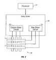
- the electronic deviceincludes a processor 21 which may be any general purpose single- or multi-chip microprocessor such as an ARM, Pentium®, Pentium II®, Pentium III®, Pentium IV®, Pentium® Pro, an 8051, a MIPS®, a Power PC®, an ALPHA®, or any special purpose microprocessor such as a digital signal processor, microcontroller, or a programmable gate array.
- the processor 21may be configured to execute one or more software modules.
- the processormay be configured to execute one or more software applications, including a web browser, a telephone application, an email program, or any other software application.
- the processor 21is also configured to communicate with an array driver 22 .
- the array driver 22includes a row driver circuit 24 and a column driver circuit 26 that provide signals to a panel or display array (display) 30 .
- the cross section of the array illustrated in FIG. 1is shown by the lines 1 - 1 in FIG. 2 .
- the row/column actuation protocolmay take advantage of a hysteresis property of these devices illustrated in FIG. 3 . It may require, for example, a 10 volt potential difference to cause a movable layer to deform from the relaxed state to the actuated state.
- the movable layermaintains its state as the voltage drops back below 10 volts.
- the movable layerdoes not relax completely until the voltage drops below 2 volts.
- There is thus a range of voltage, about 3 to 7 V in the example illustrated in FIG. 3where there exists a window of applied voltage within which the device is stable in either the relaxed or actuated state. This is referred to herein as the “hysteresis window” or “stability window.”
- the row/column actuation protocolcan be designed such that during row strobing, pixels in the strobed row that are to be actuated are exposed to a voltage difference of about 10 volts, and pixels that are to be relaxed are exposed to a voltage difference of close to zero volts. After the strobe, the pixels are exposed to a steady state voltage difference of about 5 volts such that they remain in whatever state the row strobe put them in. After being written, each pixel sees a potential difference within the “stability window” of 3-7 volts in this example. This feature makes the pixel design illustrated in FIG. 1 stable under the same applied voltage conditions in either an actuated or relaxed pre-existing state.
- each pixel of the interferometric modulatoris essentially a capacitor formed by the fixed and moving reflective layers, this stable state can be held at a voltage within the hysteresis window with almost no power dissipation. Essentially no current flows into the pixel if the applied potential is fixed.
- a display framemay be created by asserting the set of column electrodes in accordance with the desired set of actuated pixels in the first row.
- a row pulseis then applied to the row 1 electrode, actuating the pixels corresponding to the asserted column lines.
- the asserted set of column electrodesis then changed to correspond to the desired set of actuated pixels in the second row.
- a pulseis then applied to the row 2 electrode, actuating the appropriate pixels in row 2 in accordance with the asserted column electrodes.
- the row 1 pixelsare unaffected by the row 2 pulse, and remain in the state they were set to during the row 1 pulse. This may be repeated for the entire series of rows in a sequential fashion to produce the frame.
- the framesare refreshed and/or updated with new display data by continually repeating this process at some desired number of frames per second.
- protocols for driving row and column electrodes of pixel arrays to produce display framesare also well known and may be used in conjunction with the present invention.
- FIGS. 4 and 5illustrate one possible actuation protocol for creating a display frame on the 3 ⁇ 3 array of FIG. 2 .
- FIG. 4illustrates a possible set of column and row voltage levels that may be used for pixels exhibiting the hysteresis curves of FIG. 3 .
- actuating a pixelinvolves setting the appropriate column to ⁇ V bias , and the appropriate row to + ⁇ V, which may correspond to ⁇ 5 volts and +5 volts respectively. Relaxing the pixel is accomplished by setting the appropriate column to +V bias , and the appropriate row to the same + ⁇ V, producing a zero volt potential difference across the pixel.
- the pixelsare stable in whatever state they were originally in, regardless of whether the column is at +V bias , or ⁇ V bias .
- voltages of opposite polarity than those described abovecan be used, e.g., actuating a pixel can involve setting the appropriate column to +V bias , and the appropriate row to ⁇ V.
- releasing the pixelis accomplished by setting the appropriate column to ⁇ V bias , and the appropriate row to the same ⁇ V, producing a zero volt potential difference across the pixel.
- FIG. 5Bis a timing diagram showing a series of row and column signals applied to the 3 ⁇ 3 array of FIG. 2 which will result in the display arrangement illustrated in FIG. 5A , where actuated pixels are non-reflective.
- the pixelsPrior to writing the frame illustrated in FIG. 5A , the pixels can be in any state, and in this example, all the rows are at 0 volts, and all the columns are at +5 volts. With these applied voltages, all pixels are stable in their existing actuated or relaxed states.
- pixels (1,1), (1,2), (2,2), (3,2) and (3,3)are actuated.
- columns 1 and 2are set to ⁇ 5 volts
- column 3is set to +5 volts. This does not change the state of any pixels, because all the pixels remain in the 3-7 volt stability window.
- Row 1is then strobed with a pulse that goes from 0, up to 5 volts, and back to zero. This actuates the (1,1) and (1,2) pixels and relaxes the (1,3) pixel. No other pixels in the array are affected.
- column 2is set to ⁇ 5 volts
- columns 1 and 3are set to +5 volts.
- Row 3is similarly set by setting columns 2 and 3 to ⁇ 5 volts, and column 1 to +5 volts.
- the row 3 strobesets the row 3 pixels as shown in FIG. 5A .
- the row potentialsare zero, and the column potentials can remain at either +5 or ⁇ 5 volts, and the display is then stable in the arrangement of FIG. 5A . It will be appreciated that the same procedure can be employed for arrays of dozens or hundreds of rows and columns.
- FIGS. 6A and 6Bare system block diagrams illustrating an embodiment of a display device 40 .
- the display device 40can be, for example, a cellular or mobile telephone.
- the same components of display device 40 or slight variations thereofare also illustrative of various types of display devices such as televisions and portable media players.
- the display device 40includes a housing 41 , a display 30 , an antenna 43 , a speaker 45 , an input device 48 , and a microphone 46 .
- the housing 41is generally formed from any of a variety of manufacturing processes as are well known to those of skill in the art, including injection molding, and vacuum forming.
- the housing 41may be made from any of a variety of materials, including but not limited to plastic, metal, glass, rubber, and ceramic, or a combination thereof.
- the housing 41includes removable portions (not shown) that may be interchanged with other removable portions of different color, or containing different logos, pictures, or symbols.
- the display 30 of exemplary display device 40may be any of a variety of displays, including a bi-stable display, as described herein.
- the display 30includes a flat-panel display, such as plasma, EL, OLED, STN LCD, or TFT LCD as described above, or a non-flat-panel display, such as a CRT or other tube device, as is well known to those of skill in the art.
- the display 30includes an interferometric modulator display, as described herein.
- the components of one embodiment of exemplary display device 40are schematically illustrated in FIG. 6B .
- the illustrated exemplary display device 40includes a housing 41 and can include additional components at least partially enclosed therein.
- the exemplary display device 40includes a network interface 27 that includes an antenna 43 which is coupled to a transceiver 47 .
- the transceiver 47is connected to the processor 21 , which is connected to conditioning hardware 52 .
- the conditioning hardware 52may be configured to condition a signal (e.g. filter a signal).
- the conditioning hardware 52is connected to a speaker 45 and a microphone 46 .
- the processor 21is also connected to an input device 48 and a driver controller 29 .
- the driver controller 29is coupled to a frame buffer 28 and to the array driver 22 , which in turn is coupled to a display array 30 .
- a power supply 50provides power to all components as required by the particular exemplary display device 40 design.
- the network interface 27includes the antenna 43 and the transceiver 47 so that the exemplary display device 40 can communicate with one ore more devices over a network. In one embodiment the network interface 27 may also have some processing capabilities to relieve requirements of the processor 21 .
- the antenna 43is any antenna known to those of skill in the art for transmitting and receiving signals. In one embodiment, the antenna transmits and receives RF signals according to the IEEE 802.11 standard, including IEEE 802.11(a), (b), or (g). In another embodiment, the antenna transmits and receives RF signals according to the BLUETOOTH standard. In the case of a cellular telephone, the antenna is designed to receive CDMA, GSM, AMPS or other known signals that are used to communicate within a wireless cell phone network.
- the transceiver 47pre-processes the signals received from the antenna 43 so that they may be received by and further manipulated by the processor 21 .
- the transceiver 47also processes signals received from the processor 21 so that they may be transmitted from the exemplary display device 40 via the antenna 43 .
- the transceiver 47can be replaced by a receiver.
- network interface 27can be replaced by an image source, which can store or generate image data to be sent to the processor 21 .
- the image sourcecan be a digital video disc (DVD) or a hard-disc drive that contains image data, or a software module that generates image data.
- Processor 21generally controls the overall operation of the exemplary display device 40 .
- the processor 21receives data, such as compressed image data from the network interface 27 or an image source, and processes the data into raw image data or into a format that is readily processed into raw image data.
- the processor 21then sends the processed data to the driver controller 29 or to frame buffer 28 for storage.
- Raw datatypically refers to the information that identifies the image characteristics at each location within an image. For example, such image characteristics can include color, saturation, and gray-scale level.
- the processor 21includes a microcontroller, CPU, or logic unit to control operation of the exemplary display device 40 .
- Conditioning hardware 52generally includes amplifiers and filters for transmitting signals to the speaker 45 , and for receiving signals from the microphone 46 .
- Conditioning hardware 52may be discrete components within the exemplary display device 40 , or may be incorporated within the processor 21 or other components.
- the driver controller 29takes the raw image data generated by the processor 21 either directly from the processor 21 or from the frame buffer 28 and reformats the raw image data appropriately for high speed transmission to the array driver 22 . Specifically, the driver controller 29 reformats the raw image data into a data flow having a raster-like format, such that it has a time order suitable for scanning across the display array 30 . Then the driver controller 29 sends the formatted information to the array driver 22 .
- a driver controller 29such as a LCD controller, is often associated with the system processor 21 as a stand-alone Integrated Circuit (IC), such controllers may be implemented in many ways. They may be embedded in the processor 21 as hardware, embedded in the processor 21 as software, or fully integrated in hardware with the array driver 22 .
- the array driver 22receives the formatted information from the driver controller 29 and reformats the video data into a parallel set of waveforms that are applied many times per second to the hundreds and sometimes thousands of leads coming from the display's x-y matrix of pixels.
- driver controller 29is a conventional display controller or a bi-stable display controller (e.g., an interferometric modulator controller).
- array driver 22is a conventional driver or a bi-stable display driver (e.g., an interferometric modulator display).
- a driver controller 29is integrated with the array driver 22 .
- display array 30is a typical display array or a bi-stable display array (e.g., a display including an array of interferometric modulators).
- the input device 48allows a user to control the operation of the exemplary display device 40 .
- input device 48includes a keypad, such as a QWERTY keyboard or a telephone keypad, a button, a switch, a touch-sensitive screen, a pressure- or heat-sensitive membrane.
- the microphone 46is an input device for the exemplary display device 40 . When the microphone 46 is used to input data to the device, voice commands may be provided by a user for controlling operations of the exemplary display device 40 .
- Power supply 50can include a variety of energy storage devices as are well known in the art.
- power supply 50is a rechargeable battery, such as a nickel-cadmium battery or a lithium ion battery.
- power supply 50is a renewable energy source, a capacitor, or a solar cell, including a plastic solar cell, and solar-cell paint.
- power supply 50is configured to receive power from a wall outlet.
- control programmabilityresides, as described above, in a driver controller which can be located in several places in the electronic display system. In some cases control programmability resides in the array driver 22 . Those of skill in the art will recognize that the above-described optimization may be implemented in any number of hardware and/or software components and in various configurations.
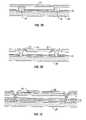
- FIGS. 7A-7Eillustrate five different embodiments of the movable reflective layer 14 and its supporting structures.
- FIG. 7Ais a cross section of the embodiment of FIG. 1 , where a strip of metal material 14 is deposited on orthogonally extending supports 18 .
- FIG. 7Bthe moveable reflective layer 14 is attached to supports at the corners only, on tethers 32 .
- FIG. 7Cthe moveable reflective layer 14 is suspended from a deformable layer 34 , which may comprise a flexible metal.
- the deformable layer 34connects, directly or indirectly, to the substrate 20 around the perimeter of the deformable layer 34 .
- connection postsare herein referred to as support posts.
- the embodiment illustrated in FIG. 7Dhas support post plugs 42 upon which the deformable layer 34 rests.
- the movable reflective layer 14remains suspended over the cavity, as in FIGS. 7A-7C , but the deformable layer 34 does not form the support posts by filling holes between the deformable layer 34 and the optical stack 16 . Rather, the support posts are formed of a planarization material, which is used to form support post plugs 42 .
- the embodiment illustrated in FIG. 7Eis based on the embodiment shown in FIG. 7D , but may also be adapted to work with any of the embodiments illustrated in FIGS. 7A-7C as well as additional embodiments not shown. In the embodiment shown in FIG. 7E , an extra layer of metal or other conductive material has been used to form a bus structure 44 . This allows signal routing along the back of the interferometric modulators, eliminating a number of electrodes that may otherwise have had to be formed on the substrate 20 .
- the interferometric modulatorsfunction as direct-view devices, in which images are viewed from the front side of the transparent substrate 20 , the side opposite to that upon which the modulator is arranged.
- the reflective layer 14optically shields some portions of the interferometric modulator on the side of the reflective layer opposite the substrate 20 , including the deformable layer 34 and the bus structure 44 . This allows the shielded areas to be configured and operated upon without negatively affecting the image quality.
- This separable modulator architectureallows the structural design and materials used for the electromechanical aspects and the optical aspects of the modulator to be selected and to function independently of each other.
- Interferometric modulatorsare typically manufactured by depositing a series of carefully defined structures onto a substrate in accordance with a set of processing parameters that is designed to produce the desired device configuration.
- the manufacturing processtypically includes, for example, a number of deposition, cleaning, masking, etching, removing, washing, doping, charging, heating, cooling, moving, storing, connecting (e.g., to other components), and/or testing steps that are carried out in a carefully planned sequence designed for efficient production.
- the individual stepsare typically known to those skilled in the art of semiconductor and/or MEMS manufacturing, although the number and type of processing steps carried out in accordance with any particular set of processing parameters may vary significantly from one manufacturing process to another, depending on the type and configuration of the device being manufactured.
- the term “set of processing parameters for manufacturing an interferometric modulator”refers to the group of individual steps and associated processing conditions used to make the particular interferometric modulator at issue, including (but not limited to) testing and integration of the resulting interferometric modulator into a device such as the display device 40 discussed above.
- the set of processing parameters used for manufacturing itare familiar with the set of processing parameters used for manufacturing it.
- FIG. 8illustrates certain steps in an embodiment of a manufacturing process 800 for an interferometric modulator. Such steps may be present in a process for manufacturing, e.g., interferometric modulators of the general type illustrated in FIGS. 1 and 7 , along with other steps not shown in FIG. 8 .
- the process 800begins at step 805 with the formation of the optical stack 16 over the substrate 20 .
- the substrate 20may be a transparent substrate such as glass or plastic and may have been subjected to prior preparation step(s), e.g., cleaning, to facilitate efficient formation of the optical stack 16 .
- the optical stack 16may be formed by employing one or more deposition steps, e.g., conductive layer (e.g., indium tin oxide) deposition, reflective layer (e.g., chromium) deposition, and dielectric layer deposition, along with one or more patterning, masking, and/or etching steps.
- conductive layere.g., indium tin oxide
- reflective layere.g., chromium
- dielectric layer depositione.g., a dielectric layer deposition
- Various charged speciesmay be generated during step 805 , e.g., by ionization during plasma-enhanced chemical vapor deposition (PECVD), and some or all of those charged species may become trapped in the optical stack 16 during deposition.
- PECVDplasma-enhanced chemical vapor deposition
- the set of processing parameters associated with the formation of the optical stack at step 805may include, e.g., cleaning, deposition (e.g., physical vapor deposition (PVD, e.g., sputter coating), PECVD, thermal chemical vapor deposition (thermal CVD), spin-coating), heating, cooling, patterning, etching and ionization.
- depositione.g., physical vapor deposition (PVD, e.g., sputter coating
- PECVDphysical chemical vapor deposition
- thermal CVDthermal chemical vapor deposition
- spin-coatinge.g., spin-coating
- the process 800 illustrated in FIG. 8continues at step 810 with the formation of a sacrificial layer over the optical stack 16 .
- the sacrificial layeris later removed (e.g., at step 825 ) to form the cavity 19 as discussed below and thus the sacrificial layer is not shown in the resulting interferometric modulator 12 illustrated in FIGS. 1 and 7 .
- the formation of the sacrificial layer over the optical stack 16may include deposition of a material such as molybdenum or amorphous silicon, in a thickness selected to provide, after subsequent removal, a cavity 19 having the desired size. Deposition of the sacrificial material may be carried out using deposition techniques such as PVD, PECVD, thermal CVD, or spin-coating.
- the set of processing parameters associated with the formation of the sacrificial layer over the optical stack at step 810may include, e.g., cleaning (e.g., cleaning of the optical stack 16 prior to deposition), deposition (e.g., PVD, PECVD, thermal CVD, spin-coating), heating, cooling, patterning, etching and ionization.
- cleaninge.g., cleaning of the optical stack 16 prior to deposition
- depositione.g., PVD, PECVD, thermal CVD, spin-coating
- heatingcooling, patterning, etching and ionization.
- the process 800 illustrated in FIG. 8continues at step 815 with the formation of a support structure e.g., a post 18 as illustrated in FIGS. 1 and 7 .
- the formation of the post 18may include the steps of patterning the sacrificial layer to form an aperture, then depositing a material (e.g., a polymer, metal or oxide) into the aperture to form the post 18 , using a deposition method such as PECVD, thermal CVD, or spin-coating.
- the upper end of the post 18may be planarized by, e.g., chemical mechanical polishing (CMP).
- CMPchemical mechanical polishing
- the set of processing parameters associated with the formation of the support structure at step 815may include, e.g., patterning, etching (e.g., forming an aperture in the sacrificial layer and the underlying optical stack 16 ), deposition (e.g., PECVD, thermal CVD, spin-coating) of the material forming the support structure, ionization, heating, cooling, and polishing.
- etchinge.g., forming an aperture in the sacrificial layer and the underlying optical stack 16
- depositione.g., PECVD, thermal CVD, spin-coating
- the process 800 illustrated in FIG. 8continues at step 820 with the formation of a moveable reflective layer such as the moveable reflective layer 14 illustrated in FIGS. 1 and 7 .
- the moveable reflective layer 14may be formed by employing one or more deposition steps, e.g., reflective layer (e.g., aluminum) deposition, along with one or more patterning, masking, and/or etching steps.
- Various charged speciesmay be generated during step 820 , e.g., by ionization during PECVD, and some or all of those charged species may become trapped in the moveable reflective layer 14 during deposition.
- the set of processing parameters associated with the formation of the moveable reflective layer at step 820may include, e.g., cleaning, deposition (e.g., PVD, PECVD, thermal CVD, spin-coating), heating, cooling, patterning, etching and ionization.
- depositione.g., PVD, PECVD, thermal CVD, spin-coating
- the process 800 illustrated in FIG. 8continues at step 825 with the formation of a cavity, e.g., a cavity 19 as illustrated in FIGS. 1 and 7 .
- the cavity 19may be formed by exposing the sacrificial material (deposited at step 810 ) to an etchant.
- a sacrificial materialsuch as molybdenum or amorphous silicon may be removed by dry chemical etching, e.g., by exposing the sacrificial layer to a gaseous or vaporous etchant such as xenon difluoride (XeF 2 ) for a period of time that is effective to remove the desired amount of material.
- XeF 2xenon difluoride
- etching methodse.g., wet etching and/or plasma etching
- Various charged speciesmay be generated during the formation of the cavity at step 825 , e.g., by ionization during PECVD, and some or all of those charged species may become trapped in the optical stack 16 and/or the moveable reflective layer 14 .
- the set of processing parameters associated with the formation of the cavity at step 825may include, e.g., heating, cooling, etching and ionization.
- Interferometric modulatorsmay be manufactured in accordance with various sets of processing parameters, and thus it will be understood that FIG. 8 shows only a few of the more common steps for the purposes of illustration. It will be also be understood that not all processes for manufacturing interferometric modulators include all the steps illustrated in FIG. 8 ; that the steps illustrated in FIG. 8 need not necessarily be carried out in the order shown, and that various additional manufacturing steps may be carried out, e.g., testing, back-end processing, and incorporating the interferometric modulator into a display device 40 as illustrated in FIG. 6 .
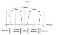
- the diagram of movable mirror position versus applied voltage shown in FIG. 3is for an idealized interferometric modulator having an offset voltage of zero.
- offset voltagerefers to the resting voltage potential present across two layers of the interferometric modulator separated by a gap.
- the offset voltagemay be determined by averaging the positive and negative actuation voltages of an interferometric modulator.
- actuation and relaxation of a pixelmay be accomplished in a symmetrical fashion. For example, as described above for the embodiment of FIG.
- actuating a pixelinvolves setting the appropriate column to ⁇ V bias , and the appropriate row to + ⁇ V, which may correspond to ⁇ 5 volts and +5 volts respectively. Relaxing the pixel is accomplished by setting the appropriate column to +V bias , and the appropriate row to the same + ⁇ V, producing a zero volt potential difference across the pixel.
- Interferometric modulatorsmay be depicted in an idealized fashion as having an offset voltage of zero, but in practice it has been discovered that existing fabrication techniques have not been adequate to reliably manufacture interferometric modulators having an offset voltage of zero. Instead, it has been discovered that interferometric modulators fabricated by existing manufacturing techniques have significant non-zero offset voltages.
- FIG. 9shows a diagram of movable mirror position versus applied voltage for an interferometric modulator having an offset voltage of 1.0 volts. It will be appreciated that an actuation protocol such as that illustrated in FIGS.
- An interferometric modulator having a non-zero offset voltagee.g., for an interferometric modulator having an offset voltage of 1.0 volts as illustrated in FIG. 9 .
- An interferometric modulator having a significant non-zero offset voltagemay require higher drive voltages and thus may have undesirably higher power consumption. For example, it is frequently desirable to consider and compensate for the non-zero offset voltage when selecting the operational voltages used to control the moveable reflective layer 14 , resulting in significantly more complicated drive schemes.
- a fixed electrical chargemay be associated with one or both of the layers 14 , 16 for interferometric modulators fabricated by existing fabrication techniques, and that this fixed electrical charge results in a non-zero offset voltage.
- charged speciesmay be trapped on or within one or both of the layers 14 , 16 during fabrication and/or subsequent processing, producing a fixed electrical charge that is manifested as a non-zero offset voltage in the resulting interferometric modulator 12 and/or the array 30 .
- the non-zero offset voltagemay also arise in other ways.
- the amount of fixed electrical charge that is associated with each layercan be modeled and used as a design criteria to select materials and/or layer configurations that minimize the amount of total offset voltage imparted to the interferometric modulator.
- FIG. 10is a process flow diagram that illustrates an embodiment of a process development method that comprises, at step 1002 , identifying a set of processing parameters for manufacturing an interferometric modulator that results in a non-zero offset voltage for the interferometric modulator.
- the set of processing parametersmay be identified in various ways.
- the set of processing parametersmay be the known processing parameters used in an existing process for manufacturing an interferometric modulator.
- the set of processing parametersare identified by modeling (e.g., computer modeling) a process for manufacturing an interferometric modulator. Suitable modeling techniques are known to those skilled in the art.
- the resulting non-zero offset voltagemay also be determined in various ways, e.g., by measuring the offset voltage of the interferometric modulator produced by the existing process and/or by modeling (e.g., computer modeling). A combination of manufacturing, testing, and/or modeling may be used to identify a suitable set of processing parameters and/or offset voltage(s).
- the process development method of FIG. 10further comprises, at step 1004 , modifying the set of processing parameters to shift the non-zero offset voltage closer to zero.
- the set of processing parametersmay be modified in various ways, e.g., by altering the value of one or more selected processing parameters, such as altering the deposition temperature and/or pressure during one or more deposition steps (e.g., the deposition temperature during deposition of a dielectric layer), altering the cleaning temperature and/or pressure during one or more cleaning steps, altering the annealing temperature and/or pressure during one or more annealing steps, and/or altering the etching temperature and/or pressure during one or more etching steps; altering the type of deposition (e.g., sputter coating, plasma-enhanced chemical vapor deposition (PECVD), thermal chemical vapor deposition, spin-coating) used to deposit one or more layers; altering an ionization parameter (e.g., changing a group of ions incorporated into a dielectric layer
- the set of processing parametersmay also be modified by adding or subtracting one or more steps from the set of processing parameters, e.g., by depositing an additional layer, by changing (or not changing) the temperature of the interferometric modulator (e.g., annealing by heating for a selected period of time, or removing an existing annealing step), by exposing (or not exposing) the interferometric modulator to a group of ions (e.g., an ionized gas such as a plasma), by passing (or not passing) a current through the interferometric modulator (e.g., by applying a counteracting current and/or a high voltage pulse), etc.
- the set of processing parametersmay be modified by any combination of changing one or more processing parameters, adding one or more processing parameters, and/or subtracting one or more processing parameters.
- the set of processing parametersmay be modified to shift the non-zero offset voltage closer to zero by implanting (or not implanting) one or more materials into one or more of the interferometric modulator layers to change the electrical characteristics of the overall interferometric modulator device.
- the optical stack 16 of an interferometric modulator of the general design illustrated in FIG. 7Ais modified to include a charged component 1005 in order to shift the non-zero offset voltage closer to zero by, e.g., obtaining a neutrally charged system.
- the charged component 1005comprises a group of positively charged ions.
- the depicted location of the charged component 1005 in the optical stack 16is illustrative, as the charged component 1005 may be incorporated into various parts of the optical stack 16 .
- the charged component 1005may be added to one or more of the various sublayers that may be present in the optical stack 16 , e.g., the dielectric sublayer 16 c and/or the metal sublayer 16 d as depicted in FIG. 11 .
- Other charged componentse.g., a group of negatively charged ions, may be used in place of or in addition to the charged component 1005 .
- the movable reflective layer 14may be modified to include a charged component 1005 (not shown in FIG. 11 ).
- the charged component 1005may also be incorporated into other types of interferometric modulators, e.g., as illustrated in FIGS. 7B-E .
- the set of processing parametersis modified to reduce or eliminate the amount of charged component incorporated into a layer during a particular processing step.
- an initial set of processing parametersmay include an ionization step (e.g., during PECVD) that results in the incorporation of a charged component into a layer.
- the set of processing parametersmay be modified to shift the non-zero offset voltage closer to zero by reducing or eliminating the ionization step so that less of the charged component is incorporated into the layer.
- a set of processing parameters that includes a step of removing the sacrificial layer by a plasma etchmay be modified by using a chemical etch (e.g., XeF 2 ) to remove the sacrificial layer instead of plasma.
- a modificationmay also include related adjustments to the materials involved, e.g., replacement of a sacrificial layer material that is removable by a plasma etch with a material that is removable by XeF 2 etching.
- the incorporation of the charged component 1005 into an interferometric modulatormay be achieved in a number of ways.
- the charged component 1005may be added to the dielectric material while the dielectric sublayer 16 c is being formed on the underlying metal sublayer 16 d .
- processing parametersexamples include changing the type of deposition, e.g., varying the deposition rate, varying the rate at which deposition gases are supplied to the process, and/or forming a dielectric layer in a PVD tool (which may produce negatively charged species that become incorporated into the dielectric layer) instead of forming the dielectric layer by chemical vapor deposition process (which may produce positively charged species that become incorporated into the dielectric layer).
- the set of processing parametersmay also be modified by altering the amount of hydrogen incorporated into the layer by, e.g., varying the amount and type of deposition gases supplied during deposition.
- the charged componentmay be added during deposition by, e.g., carrying out the deposition in the presence of charge species that become trapped within the layer 16 during deposition.
- the charged component 1005may also be added after deposition, e.g., by ion implantation. Other methods of incorporating charged components known to those skilled in the art may also be used.
- the set of processing parametersis modified to shift the non-zero offset voltage closer to zero by electrically connecting the optical stack 16 and the movable reflective layer 14 so as to minimize the charge difference between the two layers during fabrication of the interferometric modulator. This may allow for higher yield in production and higher reliability in the final interferometric modulator.
- This electrical connectionmay be removed to allow the device to properly function. In one embodiment, this connection between the two layers is created from the same material as that from which the movable reflective layer 14 is formed.
- the set of processing parametersmay be modified to shift the non-zero offset voltage closer to zero by passing a current through the interferometric modulator.
- an initial set of processing parametersmay include a step in which a current is passed through an interferometric modulator.
- Modification of the set of processing parametersmay include one or more of modifying the current, e.g., increasing the current, decreasing the current, eliminating the current, applying a counteracting current, and applying a high voltage pulse.
- counteracting currentrefers to a current that is opposite to the offset voltage bias.
- a high voltage pulseis applied for a period of time of about 1 second or less.
- a high voltage pulseis a pulse in excess of the amount typically experienced by the interferometric modulator during operation, e.g., in excess of the actuation voltage.
- modifying the currentcomprises applying a counteracting current by applying a voltage of about 10 volts or higher. In another embodiment, modifying the current comprises applying a counteracting current by applying a voltage of about 15 volts or higher.
- An interferometric modulator having a non-zero offset voltagemay be modified to shift the non-zero offset voltage closer to zero by applying a current to the interferometric modulator.
- An embodimentthus provides a method of modifying an interferometric modulator, comprising identifying an interferometric modulator having a non-zero offset voltage and applying a current to the interferometric modulator to thereby shift the non-zero offset voltage closer to zero.
- the interferometric modulator having the non-zero offset voltagemay be identified in various ways, e.g., by direct measurement of the offset voltage of a particular interferometric modulator, by modeling (e.g., by computer modeling), and/or by quality control sampling.
- a non-zero offset voltagemay be measured on a particular interferometric modulator that has characteristics representative of a batch of interferometric modulators, thereby identifying other interferometric modulators in the batch as having a non-zero offset voltage.
- Application of a current to the identified interferometric modulator to thereby shift the non-zero offset voltage closer to zeromay also be conducted in various ways as discussed above.
- the applied currentmay be a counteracting current and/or a high voltage pulse, e.g., greater than about an actuation voltage of the interferometric modulator.
- the non-zero offset voltageis sufficiently far from zero that the interferometric modulator is considered unacceptable for its intended application.
- the production of such unacceptable interferometric modulatorsmay undesirably lower manufacturing yield.
- the total number of devices N Tis the number of acceptable devices N A plus the number of unacceptable device N U .
- the manufacturing yieldis 100%.
- N Tbecomes larger than N A and the manufacturing yield falls below 100%.
- the unacceptable devicesare discarded or considered lower grade devices useable in lower value applications than originally intended.
- an embodimentprovides a method of increasing the manufacturing yield of an interferometric modulator manufacturing process by identifying an interferometric modulator having a non-zero offset voltage and applying a current to the interferometric modulator to thereby shift the non-zero offset voltage closer to zero.
- the interferometric modulator having the non-zero offset voltageconsidered unacceptable prior to application of the current, may be rendered acceptable by applying the current, thus reducing N U and increasing manufacturing yield.
- the currentmay be applied to the interferometric modulator at any stage of the manufacturing process, including after the interferometric modulator has been incorporated into a display device.
- the currentis applied to the interferometric modulator by an array driver of a display device, e.g., the array driver of the display device into which the interferometric modulator is incorporated.
- the set of processing parametersmay be modified to shift the non-zero offset voltage closer to zero by modifying or adding a processing step that comprises annealing the interferometric modulator.
- a processing stepthat comprises annealing the interferometric modulator.
- Heating the interferometric modulatormay facilitate migration and neutralization of charged components that may have become trapped within the interferometric modulator during manufacturing.
- Annealingmay be conducted by, e.g., increasing the temperature and/or time of an existing heating step, e.g., an existing annealing step or an existing heating step carried out primarily for some other purpose such as during thermal CVD, and/or by adding one or more additional heating steps. Annealing may be conducted over a broad range of temperatures and times.
- the annealing temperatures and timesare preferably selected to facilitate movement and neutralization of charged components. Shorter annealing times are typically appropriate at higher annealing temperatures, and longer annealing times are typically appropriate at lower annealing temperatures. Suitable time/temperature annealing conditions may be determined by routine experimentation. In an embodiment, annealing temperatures are in the range of about 50° C. to about 350° C., and annealing times are in the range of about one minute to about 3 hours.
- particular materialsare selected with to optimize the electrochemical characteristics of the materials.
- various work function differencesmay be used to control the final offset voltage of the interferometric modulator or change the charge accumulation rate within the device during operation of the device.
- one or both of the surfaces of the deformable layer 14 and the optical stack 16 that may come into contact during operationmay have a high work function to minimize the transfer of electrons between the layers.
- materials to be used to connect the layers 14 and 16 during processingcan be selected on the basis of their work function properties.
- FIG. 12is a process flow diagram that illustrates an embodiment of a process development method 1200 that comprises, at step 1205 , identifying a first set of processing parameters for manufacturing a first interferometric modulator.
- the first set of processing parametersmay be identified in various ways, as explained with respect to step 1002 in FIG. 10 above.
- the first set of processing parametersmay be the known processing parameters used in an existing process; in another embodiment, the first set of processing parameters may be identified by modeling (e.g., computer modeling).
- FIG. 12further illustrates, at step 1210 , continuing the process development method 1200 by determining a first offset voltage for the first interferometric modulator manufactured by the first set of processing parameters.
- the first non-zero offset voltagemay be determined in various ways, e.g., by measuring the offset voltage of the interferometric modulator produced by the existing process and/or by modeling (e.g., computer modeling).
- the process development method 1200is continued by modifying the first set of processing parameters to create a second set of processing parameters.
- the first set of processing parametersmay be modified in various ways, including by any of the ways discussed above, including modifying an existing processing parameter, adding a processing parameter and/or deleting a processing parameter.
- the second set of processing parametersis thus a modified version of the first set of processing parameters.
- FIG. 12further illustrates, at step 1220 , continuing the process development method 1200 by determining a second offset voltage for a second interferometric modulator manufactured by the second set of processing parameters.
- the second offset voltagemay also be determined in various ways, e.g., by measuring the offset voltage of a second interferometric modulator manufactured in accordance with the second set of processing parameters and/or by modeling (e.g., computer modeling).
- the second offset voltageis compared to the first offset voltage. If the second offset voltage is closer to zero than the first offset voltage, then the process development method illustrated in FIG.
- step 12has been used to successfully determine that the second set of processing parameters has been modified to shift the non-zero offset voltage closer to zero, as indicated at step 1230 . If, at step 1225 , the second offset voltage is not closer to zero than the first offset voltage, the process development method 1200 continues by returning to step 1215 . The set of processing parameters is then modified by repeating steps 1215 , 1220 and 1225 until it is determined that the modified set of processing parameters has been successfully modified to shift the non-zero offset voltage closer to zero.
- the set of processing parametersmay be modified (e.g., at steps 1004 and 1215 , respectively) in various ways.
- the set of processing parametersmay be modified by changing a single process parameter, e.g., a process condition such as deposition temperature.
- the set of processing parametersmay include a very large number of individual process parameters, such that it may be relatively time consuming to identify a modified process parameters for which the offset voltage is shifted closer to zero by changing only a single process parameter at a time.
- computer modelingmay reduce the need to carry out multiple manufacturing runs, it is often desirable to combine computer modeling with manufacturing runs.
- experimental design methodsare used to determine the effect of changing various processing parameters and combinations thereof on offset voltage.
- Experimental design methods per seare well-known, see e.g., Douglas C. Montgomery, “Design and Analysis of Experiments,” 2nd Ed., John Wiley and Sons, 1984. Experimental design methods allow various individual process parameters to be changed simultaneously. Thus, in an embodiment, the set of processing parameters is modified by using experimental design methods in which a plurality of individual process parameters are changed simultaneously.
- the process development method described above and illustrated in FIGS. 10 and 12may be used to develop a modified process for manufacturing an interferometric modulator, wherein the interferometric modulator produced by the modified process has an offset voltage that is closer to zero than an interferometric modulator produced by the unmodified process.
- an embodimentprovides a process of manufacturing an interferometric modulator, wherein the process is developed by a process development method as described herein. The individual process steps in such a process may vary, depending on the design of the particular interferometric modulator produced by the process.
- a process of manufacturing an interferometric modulatorcomprises forming an optical stack over a substrate; forming a sacrificial layer over the optical stack; forming a support structure; forming a moveable reflective layer over the sacrificial layer; and forming a cavity.
- Such a processmay be used to advantageously produce an interferometric modulator having an offset voltage that is closer to zero than interferometric modulators produced by existing processes.
- an embodimentprovides an interferometric modulator produced by such a process.
- the interferometric modulator, produced by a process developed by a process development method as described hereinhas improved performance and/or a simpler drive scheme as compared to interferometric modulators produced by existing processes.
- the interferometric modulatorproduced by a process developed by a process development method as described herein, may be incorporated into various devices, e.g., into an array of interferometric modulators and/or a display device.
- such an interferometric modulatoris incorporated into a display device as described herein, e.g., as described above with respect to FIGS. 2-6 .
Landscapes
- Physics & Mathematics (AREA)
- Engineering & Computer Science (AREA)
- General Physics & Mathematics (AREA)
- Computer Hardware Design (AREA)
- Theoretical Computer Science (AREA)
- Spectroscopy & Molecular Physics (AREA)
- Optics & Photonics (AREA)
- Mechanical Light Control Or Optical Switches (AREA)
Abstract
Description
Claims (38)
Priority Applications (8)
| Application Number | Priority Date | Filing Date | Title |
|---|---|---|---|
| US11/208,052US7327510B2 (en) | 2004-09-27 | 2005-08-19 | Process for modifying offset voltage characteristics of an interferometric modulator |
| PCT/US2005/030962WO2006036439A1 (en) | 2004-09-27 | 2005-08-31 | Process for modifying offset voltage characteristics of an interferometric modulator |
| BRPI0515291-7ABRPI0515291A (en) | 2004-09-27 | 2005-08-31 | process for modifying displacement voltage characteristics of an interferometric modulator |
| EP05792988AEP1800164A1 (en) | 2004-09-27 | 2005-08-31 | Process for modifying offset voltage characteristics of an interferometric modulator |
| AU2005290034AAU2005290034A1 (en) | 2004-09-27 | 2005-08-31 | Process for modifying offset voltage characteristics of an interferometric modulator |
| TW094132358ATW200626951A (en) | 2004-09-27 | 2005-09-19 | Process for modifying offset voltage characteristics of an interferometric modulator |
| IL180798AIL180798A0 (en) | 2004-09-27 | 2007-01-18 | Process for modifying offset voltage characteristics of an interferometric modulator |
| US11/961,744US7532386B2 (en) | 2004-09-27 | 2007-12-20 | Process for modifying offset voltage characteristics of an interferometric modulator |
Applications Claiming Priority (2)
| Application Number | Priority Date | Filing Date | Title |
|---|---|---|---|
| US61349904P | 2004-09-27 | 2004-09-27 | |
| US11/208,052US7327510B2 (en) | 2004-09-27 | 2005-08-19 | Process for modifying offset voltage characteristics of an interferometric modulator |
Related Child Applications (1)
| Application Number | Title | Priority Date | Filing Date |
|---|---|---|---|
| US11/961,744ContinuationUS7532386B2 (en) | 2004-09-27 | 2007-12-20 | Process for modifying offset voltage characteristics of an interferometric modulator |
Publications (2)
| Publication Number | Publication Date |
|---|---|
| US20060066935A1 US20060066935A1 (en) | 2006-03-30 |
| US7327510B2true US7327510B2 (en) | 2008-02-05 |
Family
ID=35447278
Family Applications (2)
| Application Number | Title | Priority Date | Filing Date |
|---|---|---|---|
| US11/208,052Expired - Fee RelatedUS7327510B2 (en) | 2004-09-27 | 2005-08-19 | Process for modifying offset voltage characteristics of an interferometric modulator |
| US11/961,744Expired - Fee RelatedUS7532386B2 (en) | 2004-09-27 | 2007-12-20 | Process for modifying offset voltage characteristics of an interferometric modulator |
Family Applications After (1)
| Application Number | Title | Priority Date | Filing Date |
|---|---|---|---|
| US11/961,744Expired - Fee RelatedUS7532386B2 (en) | 2004-09-27 | 2007-12-20 | Process for modifying offset voltage characteristics of an interferometric modulator |
Country Status (7)
| Country | Link |
|---|---|
| US (2) | US7327510B2 (en) |
| EP (1) | EP1800164A1 (en) |
| AU (1) | AU2005290034A1 (en) |
| BR (1) | BRPI0515291A (en) |
| IL (1) | IL180798A0 (en) |
| TW (1) | TW200626951A (en) |
| WO (1) | WO2006036439A1 (en) |
Cited By (229)
| Publication number | Priority date | Publication date | Assignee | Title |
|---|---|---|---|---|
| US20060066586A1 (en)* | 2004-09-27 | 2006-03-30 | Gally Brian J | Touchscreens for displays |
| US20070126673A1 (en)* | 2005-12-07 | 2007-06-07 | Kostadin Djordjev | Method and system for writing data to MEMS display elements |
| US20070147688A1 (en)* | 2005-12-22 | 2007-06-28 | Mithran Mathew | System and method for power reduction when decompressing video streams for interferometric modulator displays |
| US20080094690A1 (en)* | 2006-10-18 | 2008-04-24 | Qi Luo | Spatial Light Modulator |
| US20080094686A1 (en)* | 2006-10-19 | 2008-04-24 | U Ren Gregory David | Sacrificial spacer process and resultant structure for MEMS support structure |
| US20080093688A1 (en)* | 2004-09-27 | 2008-04-24 | Idc, Llc | Process for modifying offset voltage characteristics of an interferometric modulator |
| US20080180956A1 (en)* | 2007-01-30 | 2008-07-31 | Qualcomm Mems Technologies, Inc. | Systems and methods of providing a light guiding layer |
| US20080180783A1 (en)* | 2007-01-25 | 2008-07-31 | Li-Ming Wang | Critical dimension control for photolithography for microelectromechanical systems devices |
| US20080218843A1 (en)* | 2006-04-19 | 2008-09-11 | Qualcomm Mems Technologies,Inc. | Microelectromechanical device and method utilizing a porous surface |
| US20080226929A1 (en)* | 2006-01-18 | 2008-09-18 | Qualcomm Mems Technologies, Inc. | Silicon-rich silicon nitrides as etch stop in mems manufacture |
| US20080239449A1 (en)* | 2006-05-03 | 2008-10-02 | Qualcomm Mems Technologies, Inc. | Electrode and interconnect materials for mems devices |
| US20080252959A1 (en)* | 2003-12-09 | 2008-10-16 | Clarence Chui | Mems display |
| US20080266333A1 (en)* | 2007-01-29 | 2008-10-30 | Qualcomm Mems Technologies, Inc. | Hybrid color synthesis for multistate reflective modular displays |
| US20080311690A1 (en)* | 2007-04-04 | 2008-12-18 | Qualcomm Mems Technologies, Inc. | Eliminate release etch attack by interface modification in sacrificial layers |
| US20090002804A1 (en)* | 2007-06-29 | 2009-01-01 | Qualcomm Mems Technologies, Inc. | Electromechanical device treatment with water vapor |
| US20090009847A1 (en)* | 2007-07-05 | 2009-01-08 | Qualcomm Incorporated | Integrated imods and solar cells on a substrate |
| US20090051925A1 (en)* | 2006-06-30 | 2009-02-26 | Qualcomm Mems Technologies, Inc. | Determination of interferometric modulator mirror curvature and airgap variation using digital photographs |
| US20090059345A1 (en)* | 2006-03-02 | 2009-03-05 | Qualcomm Mems Technologies, Inc. | Mems devices with protective coatings |
| US20090062131A1 (en)* | 2003-10-02 | 2009-03-05 | Wyeth | Nucleic acid arrays for detecting gene expression in animal models of inflammatory diseases |
| US20090071933A1 (en)* | 2007-09-14 | 2009-03-19 | Qualcomm Mems Technologies, Inc. | Etching processes used in mems production |
| US20090073534A1 (en)* | 2007-09-14 | 2009-03-19 | Donovan Lee | Interferometric modulator display devices |
| US20090078316A1 (en)* | 2007-09-24 | 2009-03-26 | Qualcomm Incorporated | Interferometric photovoltaic cell |
| US20090088619A1 (en)* | 2007-10-01 | 2009-04-02 | Quantum Applied Science & Research, Inc. | Self-Locating Sensor Mounting Apparatus |
| US20090101192A1 (en)* | 2007-10-19 | 2009-04-23 | Qualcomm Incorporated | Photovoltaic devices with integrated color interferometric film stacks |
| US20090103165A1 (en)* | 2007-10-19 | 2009-04-23 | Qualcomm Mems Technologies, Inc. | Display with Integrated Photovoltaics |
| US20090103166A1 (en)* | 2007-10-23 | 2009-04-23 | Qualcomm Mems Technologies, Inc. | Adjustably transmissive mems-based devices |
| US20090126792A1 (en)* | 2007-11-16 | 2009-05-21 | Qualcomm Incorporated | Thin film solar concentrator/collector |
| US20090126777A1 (en)* | 2007-11-16 | 2009-05-21 | Qualcomm Mems Technologies, Inc. | Simultaneous light collection and illumination on an active display |
| US20090135466A1 (en)* | 2004-09-27 | 2009-05-28 | Idc, Llc | Method and device for multistate interferometric light modulation |
| US20090135465A1 (en)* | 2004-09-27 | 2009-05-28 | Idc, Llc | System and method for multi-level brightness in interferometric modulation |
| US20090147343A1 (en)* | 2007-12-07 | 2009-06-11 | Lior Kogut | Mems devices requiring no mechanical support |
| US7547565B2 (en) | 2005-02-04 | 2009-06-16 | Qualcomm Mems Technologies, Inc. | Method of manufacturing optical interference color display |
| US20090151771A1 (en)* | 2007-12-17 | 2009-06-18 | Qualcomm Mems Technologies, Inc. | Photovoltaics with interferometric ribbon masks |
| US20090159123A1 (en)* | 2007-12-21 | 2009-06-25 | Qualcomm Mems Technologies, Inc. | Multijunction photovoltaic cells |
| US20090168459A1 (en)* | 2007-12-27 | 2009-07-02 | Qualcomm Incorporated | Light guide including conjugate film |
| US7556981B2 (en) | 2006-12-29 | 2009-07-07 | Qualcomm Mems Technologies, Inc. | Switches for shorting during MEMS etch release |
| US7561321B2 (en) | 2006-06-01 | 2009-07-14 | Qualcomm Mems Technologies, Inc. | Process and structure for fabrication of MEMS device having isolated edge posts |
| US20090201008A1 (en)* | 2008-02-11 | 2009-08-13 | Qualcomm Mems Technologies, Inc. | Methods for measurement and characterization of interferometric modulators |
| US20090199900A1 (en)* | 2008-02-12 | 2009-08-13 | Qualcomm Mems Technologies, Inc. | Thin film holographic solar concentrator/collector |
| US20090204350A1 (en)* | 2008-02-11 | 2009-08-13 | Qualcomms Technologies, Inc, | Methods for measurement and characterization of interferometric modulators |
| US20090201318A1 (en)* | 2008-02-13 | 2009-08-13 | Qualcomm Mems Technologies, Inc. | Multi-level stochastic dithering with noise mitigation via sequential template averaging |
| US20090201282A1 (en)* | 2008-02-11 | 2009-08-13 | Qualcomm Mems Technologies, Inc | Methods of tuning interferometric modulator displays |
| US20090201301A1 (en)* | 2008-02-12 | 2009-08-13 | Qualcomm Mems Technologies, Inc. | Integrated front light solution |
| US20090201242A1 (en)* | 2008-02-11 | 2009-08-13 | Qualcomm Mems Technologies, Inc. | Sensing to determine pixel state in a passively addressed display array |
| US20090201571A1 (en)* | 2008-02-12 | 2009-08-13 | Qualcomm Mems Technologies, Inc. | Integrated front light diffuser for reflective displays |
| US20090204349A1 (en)* | 2008-02-11 | 2009-08-13 | Qualcomm Mems Technologies, Inc. | Measurement and apparatus for electrical measurement of electrical drive parameters for a mems based display |
| US20090207159A1 (en)* | 2008-02-11 | 2009-08-20 | Qualcomm Mems Technologies, Inc. | Method and apparatus for sensing, measurement or characterization of display elements integrated with the display drive scheme, and system and applications using the same |
| US7580172B2 (en) | 2005-09-30 | 2009-08-25 | Qualcomm Mems Technologies, Inc. | MEMS device and interconnects for same |
| US20090213451A1 (en)* | 2006-06-30 | 2009-08-27 | Qualcomm Mems Technology, Inc. | Method of manufacturing mems devices providing air gap control |
| US20090219604A1 (en)* | 1999-10-05 | 2009-09-03 | Qualcomm Mems Technologies, Inc. | Photonic mems and structures |
| US20090224748A1 (en)* | 2004-08-27 | 2009-09-10 | Idc, Llc | System and method of sensing actuation and release voltages of an interferometric modulator |
| US20090225395A1 (en)* | 2008-03-07 | 2009-09-10 | Qualcomm Mems Technologies, Inc. | Interferometric modulator in transmission mode |
| US20090231816A1 (en)* | 2008-03-07 | 2009-09-17 | Qualcomm Mems Technologies, Inc. | System and method of preventing damage to metal traces of flexible printed circuits |
| US20090237040A1 (en)* | 2008-03-18 | 2009-09-24 | Qualcomm Mems Technologies, Inc. | family of current/power-efficient high voltage linear regulator circuit architectures |
| US20090242836A1 (en)* | 2007-12-06 | 2009-10-01 | Jean-Pierre Tahon | X-ray imaging photostimulable phosphor screen or panel |
| US20090244679A1 (en)* | 2008-03-27 | 2009-10-01 | Qualcomm Mems Technologies, Inc. | Dimming mirror |
| US20090244683A1 (en)* | 2008-03-28 | 2009-10-01 | Qualcomm Mems Technologies, Inc. | Apparatus and method of dual-mode display |
| US20090244680A1 (en)* | 2008-03-31 | 2009-10-01 | Qualcomm Mems Technologies, Inc. | Human-readable, bi-state environmental sensors based on micro-mechanical membranes |
| US20090251761A1 (en)* | 2008-04-02 | 2009-10-08 | Kasra Khazeni | Microelectromechanical systems display element with photovoltaic structure |
| US20090251752A1 (en)* | 2006-10-10 | 2009-10-08 | Qualcomm Mems Technologies, Inc. | Display device with diffractive optics |
| US20090255569A1 (en)* | 2008-04-11 | 2009-10-15 | Qualcomm Mems Technologies, Inc. | Method to improve pv aesthetics and efficiency |
| US20090257105A1 (en)* | 2008-04-10 | 2009-10-15 | Qualcomm Mems Technologies, Inc. | Device having thin black mask and method of fabricating the same |
| US7612933B2 (en) | 2008-03-27 | 2009-11-03 | Qualcomm Mems Technologies, Inc. | Microelectromechanical device with spacing layer |
| US20090273824A1 (en)* | 2007-05-09 | 2009-11-05 | Qualcomm Mems Techologies, Inc. | Electromechanical system having a dielectric movable membrane |
| US20090279174A1 (en)* | 2008-05-07 | 2009-11-12 | Qualcomm Mems Technologies, Inc. | Printable static interferometric images |
| US20090293955A1 (en)* | 2007-11-07 | 2009-12-03 | Qualcomm Incorporated | Photovoltaics with interferometric masks |
| US20090305010A1 (en)* | 2008-06-05 | 2009-12-10 | Qualcomm Mems Technologies, Inc. | Low temperature amorphous silicon sacrificial layer for controlled adhesion in mems devices |
| US20090303746A1 (en)* | 2008-06-04 | 2009-12-10 | Qualcomm Mems Technologies, Inc. | Edge shadow reducing methods for prismatic front light |
| US20090319218A1 (en)* | 2008-06-24 | 2009-12-24 | Qualcomm Mems Technologies, Inc. | Apparatus, method and computer-readable medium for testing a panel of interferometric modulators |
| US20090315567A1 (en)* | 2006-02-22 | 2009-12-24 | Qualcomm Mems Technologies, Inc. | Electrical conditioning of mems device and insulating layer thereof |
| US20090319220A1 (en)* | 2008-06-18 | 2009-12-24 | Qualcomm Mems Technologies, Inc. | Pressure measurement using a mems device |
| US20090317946A1 (en)* | 2006-02-21 | 2009-12-24 | Qualcomm Mems Technologies, Inc. | Method for providing and removing discharging interconnect for chip-on-glass output leads and structures thereof |
| US20090323144A1 (en)* | 2008-06-30 | 2009-12-31 | Qualcomm Mems Technologies, Inc. | Illumination device with holographic light guide |
| US20090323154A1 (en)* | 2008-06-25 | 2009-12-31 | Qualcomm Mems Technologies, Inc. | Backlight displays |
| US20090323170A1 (en)* | 2008-06-30 | 2009-12-31 | Qualcomm Mems Technologies, Inc. | Groove on cover plate or substrate |
| US20090323153A1 (en)* | 2008-06-25 | 2009-12-31 | Qualcomm Mems Technologies, Inc. | Backlight displays |
| US20090323165A1 (en)* | 2008-06-25 | 2009-12-31 | Qualcomm Mems Technologies, Inc. | Method for packaging a display device and the device obtained thereof |
| US20100014146A1 (en)* | 2008-07-17 | 2010-01-21 | Qualcomm Mems Technologies, Inc. | Encapsulation methods for interferometric modulator and mems devices |
| US7652814B2 (en) | 2006-01-27 | 2010-01-26 | Qualcomm Mems Technologies, Inc. | MEMS device with integrated optical element |
| US20100019336A1 (en)* | 2005-07-22 | 2010-01-28 | Qualcomm Mems Technologies, Inc. | Mems devices having overlying support structures and methods of fabricating the same |
| US20100020382A1 (en)* | 2008-07-22 | 2010-01-28 | Qualcomm Mems Technologies, Inc. | Spacer for mems device |
| US20100026727A1 (en)* | 2006-10-06 | 2010-02-04 | Qualcomm Mems Technologies, Inc. | Optical loss structure integrated in an illumination apparatus |
| US20100046058A1 (en)* | 2005-10-28 | 2010-02-25 | Qualcomm Mems Technologies, Inc. | Diffusion barrier layer for mems devices |
| US20100053148A1 (en)* | 2008-09-02 | 2010-03-04 | Qualcomm Mems Technologies, Inc. | Light turning device with prismatic light turning features |
| US20100079847A1 (en)* | 2008-09-30 | 2010-04-01 | Qualcomm Mems Technologies, Inc. | Multi-thickness layers for mems and mask-saving sequence for same |
| US20100096011A1 (en)* | 2008-10-16 | 2010-04-22 | Qualcomm Mems Technologies, Inc. | High efficiency interferometric color filters for photovoltaic modules |
| US20100096006A1 (en)* | 2008-10-16 | 2010-04-22 | Qualcomm Mems Technologies, Inc. | Monolithic imod color enhanced photovoltaic cell |
| US20100108056A1 (en)* | 2008-11-06 | 2010-05-06 | Industrial Technology Research Institute | Solar energy collecting module |
| US20100118382A1 (en)* | 2006-06-01 | 2010-05-13 | Qualcomm Mems Technologies, Inc. | Analog interferometric modulator device with electrostatic actuation and release |
| US20100128339A1 (en)* | 2006-04-10 | 2010-05-27 | Qualcomm Mems Technologies, Inc. | Interferometric optical display system with broadband characteristics |
| US20100128337A1 (en)* | 2008-07-11 | 2010-05-27 | Yeh-Jiun Tung | Stiction mitigation with integrated mech micro-cantilevers through vertical stress gradient control |
| US20100134503A1 (en)* | 2004-09-27 | 2010-06-03 | Qualcomm Mems Technologies, Inc. | Controller and driver features for bi-stable display |
| US20100141557A1 (en)* | 2006-10-06 | 2010-06-10 | Qualcomm Mems Technologies, Inc. | Light guide |
| US20100147790A1 (en)* | 2005-07-22 | 2010-06-17 | Qualcomm Mems Technologies, Inc. | Support structure for mems device and methods therefor |
| US20100157406A1 (en)* | 2008-12-19 | 2010-06-24 | Qualcomm Mems Technologies, Inc. | System and method for matching light source emission to display element reflectivity |
| US20100177533A1 (en)* | 2009-01-13 | 2010-07-15 | Qualcomm Mems Technologies, Inc. | Large area light panel and screen |
| US20100180946A1 (en)* | 2008-09-18 | 2010-07-22 | Qualcomm Mems Technologies, Inc. | Increasing the angular range of light collection in solar collectors/concentrators |
| US20100182308A1 (en)* | 2006-10-06 | 2010-07-22 | Holman Robert L | Light bar including turning microstructures and contoured back reflector |
| US20100182675A1 (en)* | 2007-05-11 | 2010-07-22 | Qualcomm Mems Technologies, Inc. | Methods of fabricating mems with spacers between plates and devices formed by same |
| US20100187422A1 (en)* | 2009-01-23 | 2010-07-29 | Qualcomm Mems Technologies, Inc. | Integrated light emitting and light detecting device |
| US20100188443A1 (en)* | 2007-01-19 | 2010-07-29 | Pixtronix, Inc | Sensor-based feedback for display apparatus |
| US7768690B2 (en) | 2008-06-25 | 2010-08-03 | Qualcomm Mems Technologies, Inc. | Backlight displays |
| US20100200938A1 (en)* | 2005-08-19 | 2010-08-12 | Qualcomm Mems Technologies, Inc. | Methods for forming layers within a mems device using liftoff processes |
| US20100202038A1 (en)* | 2006-12-20 | 2010-08-12 | Qualcomm Mems Technologies, Inc. | Mems device and interconnects for same |
| US20100206629A1 (en)* | 2009-02-13 | 2010-08-19 | Qualcomm Mems Technologies, Inc. | Display device with desiccant |
| US20100214642A1 (en)* | 1995-11-06 | 2010-08-26 | Miles Mark W | Method and device for modulating light with optical compensation |
| US7787130B2 (en) | 2008-03-31 | 2010-08-31 | Qualcomm Mems Technologies, Inc. | Human-readable, bi-state environmental sensors based on micro-mechanical membranes |
| US20100219155A1 (en)* | 2007-02-20 | 2010-09-02 | Qualcomm Mems Technologies, Inc. | Equipment and methods for etching of mems |
| US20100231510A1 (en)* | 2007-04-30 | 2010-09-16 | Qualcomm Mems Technologies, Inc. | Dual film light guide for illuminating displays |
| US20100238572A1 (en)* | 2009-03-23 | 2010-09-23 | Qualcomm Mems Technologies, Inc. | Display device with openings between sub-pixels and method of making same |
| US20100238537A1 (en)* | 2007-11-12 | 2010-09-23 | Qualcomm Mems Technologies, Inc. | Capacitive mems device with programmable offset voltage control |
| US20100245979A1 (en)* | 2007-03-21 | 2010-09-30 | Qualcomm Mems Technologies, Inc. | Mems cavity-coating layers and methods |
| US20100245311A1 (en)* | 2009-03-27 | 2010-09-30 | Qualcomm Mems Technologies, Inc. | Low voltage driver scheme for interferometric modulators |
| US20100245338A1 (en)* | 2009-03-27 | 2010-09-30 | Qualcomm Mems Technologies, Inc. | Frame rates in a mems display by selective line skipping |
| US20100245977A1 (en)* | 2009-03-27 | 2010-09-30 | Qualcomm Mems Technologies, Inc. | Post-release adjustment of interferometric modulator reflectivity |
| US20100245313A1 (en)* | 2009-03-27 | 2010-09-30 | Qualcomm Mems Technologies, Inc. | Low voltage driver scheme for interferometric modulators |
| US20100245833A1 (en)* | 2009-03-24 | 2010-09-30 | Qualcomm Mems Technologies, Inc. | System and method for measuring display quality with a hyperspectral imager |
| US20100245370A1 (en)* | 2009-03-25 | 2010-09-30 | Qualcomm Mems Technologies, Inc. | Em shielding for display devices |
| US7808695B2 (en) | 2006-06-15 | 2010-10-05 | Qualcomm Mems Technologies, Inc. | Method and apparatus for low range bit depth enhancement for MEMS display architectures |
| US20100271688A1 (en)* | 2005-12-29 | 2010-10-28 | Qualcomm Mems Technologies, Inc. | Method of creating mems device cavities by a non-etching process |
| US20100302802A1 (en)* | 2009-05-29 | 2010-12-02 | QUALCOMM MEMS Tecnologies, Inc. | Illumination devices |
| US20100309572A1 (en)* | 2007-09-14 | 2010-12-09 | Qualcomm Mems Technologies, Inc. | Periodic dimple array |
| US7852491B2 (en) | 2008-03-31 | 2010-12-14 | Qualcomm Mems Technologies, Inc. | Human-readable, bi-state environmental sensors based on micro-mechanical membranes |
| US20100315833A1 (en)* | 2008-01-30 | 2010-12-16 | Digital Optics International Llc | Thin illumination system |
| US20100315696A1 (en)* | 2009-06-15 | 2010-12-16 | Qualcomm Mems Technologies, Inc. | Analog interferometric modulator |
| US7855826B2 (en) | 2008-08-12 | 2010-12-21 | Qualcomm Mems Technologies, Inc. | Method and apparatus to reduce or eliminate stiction and image retention in interferometric modulator devices |
| US20100321352A1 (en)* | 2006-06-29 | 2010-12-23 | Qualcomm Mems Technologies, Inc. | Passive circuits for de-multiplexing display inputs |
| US7863079B2 (en) | 2008-02-05 | 2011-01-04 | Qualcomm Mems Technologies, Inc. | Methods of reducing CD loss in a microelectromechanical device |
| US20110012219A1 (en)* | 2007-09-28 | 2011-01-20 | Qualcomm Mems Technologies, Inc. | Optimization of desiccant usage in a mems package |
| US20110026095A1 (en)* | 2007-07-31 | 2011-02-03 | Qualcomm Mems Technologies, Inc. | Devices and methods for enhancing color shift of interferometric modulators |
| US20110025727A1 (en)* | 2009-08-03 | 2011-02-03 | Qualcomm Mems Technologies, Inc. | Microstructures for light guide illumination |
| US20110032427A1 (en)* | 2009-06-05 | 2011-02-10 | Qualcomm Mems Technologies, Inc. | System and method for improving the quality of halftone video using a fixed threshold |
| US20110032214A1 (en)* | 2009-06-01 | 2011-02-10 | Qualcomm Mems Technologies, Inc. | Front light based optical touch screen |
| US20110053304A1 (en)* | 2004-05-12 | 2011-03-03 | Qualcomm Mems Technologies, Inc. | Method of making an electronic device with a curved backplate |
| US7903316B2 (en) | 2007-07-25 | 2011-03-08 | Qualcomm Mems Technologies, Inc. | MEMS display devices and methods of fabricating the same |
| US7903047B2 (en) | 2006-04-17 | 2011-03-08 | Qualcomm Mems Technologies, Inc. | Mode indicator for interferometric modulator displays |
| US20110063712A1 (en)* | 2009-09-17 | 2011-03-17 | Qualcomm Mems Technologies, Inc. | Display device with at least one movable stop element |
| US20110075241A1 (en)* | 2009-09-28 | 2011-03-31 | Qualcomm Mems Technologies, Inc. | Interferometric display with interferometric reflector |
| US7920319B2 (en) | 2007-07-02 | 2011-04-05 | Qualcomm Mems Technologies, Inc. | Electromechanical device with optical function separated from mechanical and electrical function |
| US20110096508A1 (en)* | 2009-10-23 | 2011-04-28 | Qualcomm Mems Technologies, Inc. | Light-based sealing and device packaging |
| US20110102800A1 (en)* | 2009-11-05 | 2011-05-05 | Qualcomm Mems Technologies, Inc. | Methods and devices for detecting and measuring environmental conditions in high performance device packages |
| US20110109615A1 (en)* | 2009-11-12 | 2011-05-12 | Qualcomm Mems Technologies, Inc. | Energy saving driving sequence for a display |
| US20110113616A1 (en)* | 2009-11-16 | 2011-05-19 | Qualcomm Mems Technologies, Inc. | System and method for manufacturing a display device having an electrically connected front plate and back plate |
| US20110128307A1 (en)* | 2004-09-27 | 2011-06-02 | Qualcomm Mems Technologies, Inc. | Method and device for manipulating color in a display |
| US20110148751A1 (en)* | 2004-09-27 | 2011-06-23 | Qualcomm Mems Technologies, Inc. | Method and device for manipulating color in a display |
| US7969641B2 (en) | 2008-02-14 | 2011-06-28 | Qualcomm Mems Technologies, Inc. | Device having power generating black mask and method of fabricating the same |
| US20110157093A1 (en)* | 2009-12-29 | 2011-06-30 | Qualcomm Mems Technologies, Inc. | Illumination device with metalized light-turning features |
| US20110164014A1 (en)* | 2010-01-06 | 2011-07-07 | Qualcomm Mems Technologies, Inc. | Display drive switch configuration |
| US20110164068A1 (en)* | 2010-01-06 | 2011-07-07 | Qualcomm Mems Technologies, Inc. | Reordering display line updates |
| US20110164009A1 (en)* | 2010-01-06 | 2011-07-07 | Qualcomm Mems Technologies, Inc. | Charge pump for producing display driver output |
| US20110164027A1 (en)* | 2010-01-06 | 2011-07-07 | Qualcomm Mems Technologies, Inc. | Method of detecting change in display data |
| US20110169428A1 (en)* | 2010-01-08 | 2011-07-14 | Qualcomm Mems Technologies, Inc. | Edge bar designs to mitigate edge shadow artifact |
| US20110177745A1 (en)* | 2006-01-13 | 2011-07-21 | Qualcomm Mems Technologies, Inc. | Interconnect structure for mems device |
| US20110176196A1 (en)* | 2010-01-15 | 2011-07-21 | Qualcomm Mems Technologies, Inc. | Methods and devices for pressure detection |
| US20110182086A1 (en)* | 2007-12-07 | 2011-07-28 | Qualcomm Incorporated | Light illumination of displays with front light guide and coupling elements |
| US20110193770A1 (en)* | 2004-09-27 | 2011-08-11 | Qualcomm Mems Technologies, Inc. | Device and method for wavelength filtering |
| US20110199667A1 (en)* | 2006-02-17 | 2011-08-18 | Qualcomm Mems Technologies, Inc. | Method and apparatus for lighting a display device |
| US8004514B2 (en) | 2006-02-10 | 2011-08-23 | Qualcomm Mems Technologies, Inc. | Method and system for updating of displays showing deterministic content |
| US20110221798A1 (en)* | 2010-03-12 | 2011-09-15 | Qualcomm Mems Technologies, Inc. | Line multiplying to enable increased refresh rate of a display |
| US20110227937A1 (en)* | 2010-03-17 | 2011-09-22 | Qualcomm Mems Technologies, Inc. | System and method for frame buffer storage and retrieval in alternating orientations |
| US20110235155A1 (en)* | 2010-03-25 | 2011-09-29 | Qualcomm Mems Technologies, Inc. | Mechanical layer and methods of shaping the same |
| US20110235156A1 (en)* | 2010-03-26 | 2011-09-29 | Qualcomm Mems Technologies, Inc. | Methods and devices for pressure detection |
| WO2011130718A2 (en) | 2010-04-16 | 2011-10-20 | Flex Lighting Ii, Llc | Front illumination device comprising a film-based lightguide |
| WO2011130715A2 (en) | 2010-04-16 | 2011-10-20 | Flex Lighting Ii, Llc | Illumination device comprising a film-based lightguide |
| US8077326B1 (en) | 2008-03-31 | 2011-12-13 | Qualcomm Mems Technologies, Inc. | Human-readable, bi-state environmental sensors based on micro-mechanical membranes |
| US20110316832A1 (en)* | 2010-06-24 | 2011-12-29 | Qualcomm Mems Technologies, Inc. | Pixel drive scheme having improved release characteristics |
| US8164821B2 (en) | 2008-02-22 | 2012-04-24 | Qualcomm Mems Technologies, Inc. | Microelectromechanical device with thermal expansion balancing layer or stiffening layer |
| US8294184B2 (en) | 2011-02-23 | 2012-10-23 | Qualcomm Mems Technologies, Inc. | EMS tunable transistor |
| US8346048B2 (en) | 2008-05-28 | 2013-01-01 | Qualcomm Mems Technologies, Inc. | Front light devices and methods of fabrication thereof |
| US8345030B2 (en) | 2011-03-18 | 2013-01-01 | Qualcomm Mems Technologies, Inc. | System and method for providing positive and negative voltages from a single inductor |
| US8390916B2 (en) | 2010-06-29 | 2013-03-05 | Qualcomm Mems Technologies, Inc. | System and method for false-color sensing and display |
| US8402647B2 (en) | 2010-08-25 | 2013-03-26 | Qualcomm Mems Technologies Inc. | Methods of manufacturing illumination systems |
| US8411026B2 (en) | 2004-09-27 | 2013-04-02 | Qualcomm Mems Technologies, Inc. | Methods and devices for lighting displays |
| US8416154B2 (en) | 2004-09-27 | 2013-04-09 | Qualcomm Mems Technologies, Inc. | Apparatus and method for reducing perceived color shift |
| US20130100097A1 (en)* | 2011-10-21 | 2013-04-25 | Qualcomm Mems Technologies, Inc. | Device and method of controlling lighting of a display based on ambient lighting conditions |
| US8437070B2 (en) | 2004-09-27 | 2013-05-07 | Qualcomm Mems Technologies, Inc. | Interferometric modulator with dielectric layer |
| US8445390B1 (en) | 2011-11-10 | 2013-05-21 | Qualcomm Mems Technologies, Inc. | Patterning of antistiction films for electromechanical systems devices |
| US8514169B2 (en) | 2004-09-27 | 2013-08-20 | Qualcomm Mems Technologies, Inc. | Apparatus and system for writing data to electromechanical display elements |
| US8638491B2 (en) | 2004-09-27 | 2014-01-28 | Qualcomm Mems Technologies, Inc. | Device having a conductive light absorbing mask and method for fabricating same |
| US8643936B2 (en) | 2011-05-04 | 2014-02-04 | Qualcomm Mems Technologies, Inc. | Devices and methods for achieving non-contacting white state in interferometric modulators |
| US8659816B2 (en) | 2011-04-25 | 2014-02-25 | Qualcomm Mems Technologies, Inc. | Mechanical layer and methods of making the same |
| US8669926B2 (en) | 2011-11-30 | 2014-03-11 | Qualcomm Mems Technologies, Inc. | Drive scheme for a display |
| US8670171B2 (en) | 2010-10-18 | 2014-03-11 | Qualcomm Mems Technologies, Inc. | Display having an embedded microlens array |
| US8674616B2 (en) | 2008-10-10 | 2014-03-18 | Qualcomm Mems Technologies, Inc. | Distributed illumination system |
| US8714023B2 (en) | 2011-03-10 | 2014-05-06 | Qualcomm Mems Technologies, Inc. | System and method for detecting surface perturbations |
| US8721149B2 (en) | 2008-01-30 | 2014-05-13 | Qualcomm Mems Technologies, Inc. | Illumination device having a tapered light guide |
| US8736939B2 (en) | 2011-11-04 | 2014-05-27 | Qualcomm Mems Technologies, Inc. | Matching layer thin-films for an electromechanical systems reflective display device |
| US8735225B2 (en) | 2004-09-27 | 2014-05-27 | Qualcomm Mems Technologies, Inc. | Method and system for packaging MEMS devices with glass seal |
| US8742570B2 (en) | 2011-09-09 | 2014-06-03 | Qualcomm Mems Technologies, Inc. | Backplate interconnect with integrated passives |
| US8749538B2 (en) | 2011-10-21 | 2014-06-10 | Qualcomm Mems Technologies, Inc. | Device and method of controlling brightness of a display based on ambient lighting conditions |
| US8760751B2 (en) | 2012-01-26 | 2014-06-24 | Qualcomm Mems Technologies, Inc. | Analog IMOD having a color notch filter |
| US8780104B2 (en) | 2011-03-15 | 2014-07-15 | Qualcomm Mems Technologies, Inc. | System and method of updating drive scheme voltages |
| US8786592B2 (en) | 2011-10-13 | 2014-07-22 | Qualcomm Mems Technologies, Inc. | Methods and systems for energy recovery in a display |
| US8791897B2 (en) | 2004-09-27 | 2014-07-29 | Qualcomm Mems Technologies, Inc. | Method and system for writing data to MEMS display elements |
| US8798425B2 (en) | 2007-12-07 | 2014-08-05 | Qualcomm Mems Technologies, Inc. | Decoupled holographic film and diffuser |
| US8797632B2 (en) | 2010-08-17 | 2014-08-05 | Qualcomm Mems Technologies, Inc. | Actuation and calibration of charge neutral electrode of a display device |
| US8803861B2 (en) | 2012-02-23 | 2014-08-12 | Qualcomm Mems Technologies, Inc. | Electromechanical systems device |
| US8817357B2 (en) | 2010-04-09 | 2014-08-26 | Qualcomm Mems Technologies, Inc. | Mechanical layer and methods of forming the same |
| US8836681B2 (en) | 2011-10-21 | 2014-09-16 | Qualcomm Mems Technologies, Inc. | Method and device for reducing effect of polarity inversion in driving display |
| US8848294B2 (en) | 2010-05-20 | 2014-09-30 | Qualcomm Mems Technologies, Inc. | Method and structure capable of changing color saturation |
| US8847862B2 (en) | 2011-11-29 | 2014-09-30 | Qualcomm Mems Technologies, Inc. | Systems, devices, and methods for driving an interferometric modulator |
| US8861071B2 (en) | 2004-09-27 | 2014-10-14 | Qualcomm Mems Technologies, Inc. | Method and device for compensating for color shift as a function of angle of view |
| US8872804B2 (en) | 2011-07-21 | 2014-10-28 | Qualcomm Mems Technologies, Inc. | Touch sensing display devices and related methods |
| US8878771B2 (en) | 2004-09-27 | 2014-11-04 | Qualcomm Mems Technologies, Inc. | Method and system for reducing power consumption in a display |
| US8885244B2 (en) | 2004-09-27 | 2014-11-11 | Qualcomm Mems Technologies, Inc. | Display device |
| US8902484B2 (en) | 2010-12-15 | 2014-12-02 | Qualcomm Mems Technologies, Inc. | Holographic brightness enhancement film |
| US8904867B2 (en) | 2010-11-04 | 2014-12-09 | Qualcomm Mems Technologies, Inc. | Display-integrated optical accelerometer |
| US8911102B2 (en) | 2012-06-29 | 2014-12-16 | Qualcomm Mems Technologies, Inc. | Low-profile lighting system |
| US8928967B2 (en) | 1998-04-08 | 2015-01-06 | Qualcomm Mems Technologies, Inc. | Method and device for modulating light |
| US8963159B2 (en) | 2011-04-04 | 2015-02-24 | Qualcomm Mems Technologies, Inc. | Pixel via and methods of forming the same |
| US8970767B2 (en) | 2011-06-21 | 2015-03-03 | Qualcomm Mems Technologies, Inc. | Imaging method and system with angle-discrimination layer |
| US8970939B2 (en) | 2004-09-27 | 2015-03-03 | Qualcomm Mems Technologies, Inc. | Method and device for multistate interferometric light modulation |
| US8979349B2 (en) | 2009-05-29 | 2015-03-17 | Qualcomm Mems Technologies, Inc. | Illumination devices and methods of fabrication thereof |
| US8988409B2 (en) | 2011-07-22 | 2015-03-24 | Qualcomm Mems Technologies, Inc. | Methods and devices for voltage reduction for active matrix displays using variability of pixel device capacitance |
| US8995043B2 (en) | 2011-11-29 | 2015-03-31 | Qualcomm Mems Technologies, Inc. | Interferometric modulator with dual absorbing layers |
| US9001412B2 (en) | 2004-09-27 | 2015-04-07 | Qualcomm Mems Technologies, Inc. | Electromechanical device with optical function separated from mechanical and electrical function |
| US9019590B2 (en) | 2004-02-03 | 2015-04-28 | Qualcomm Mems Technologies, Inc. | Spatial light modulator with integrated optical compensation structure |
| US9019240B2 (en) | 2011-09-29 | 2015-04-28 | Qualcomm Mems Technologies, Inc. | Optical touch device with pixilated light-turning features |
| US9025235B2 (en) | 2002-12-25 | 2015-05-05 | Qualcomm Mems Technologies, Inc. | Optical interference type of color display having optical diffusion layer between substrate and electrode |
| US9030391B2 (en) | 2011-11-30 | 2015-05-12 | Qualcomm Mems Technologies, Inc. | Systems, devices, and methods for driving an analog interferometric modulator |
| US9035934B2 (en) | 2012-05-02 | 2015-05-19 | Qualcomm Mems Technologies, Inc. | Voltage biased pull analog interferometric modulator with charge injection control |
| US9057872B2 (en) | 2010-08-31 | 2015-06-16 | Qualcomm Mems Technologies, Inc. | Dielectric enhanced mirror for IMOD display |
| US9086564B2 (en) | 2004-09-27 | 2015-07-21 | Qualcomm Mems Technologies, Inc. | Conductive bus structure for interferometric modulator array |
| US9110289B2 (en) | 1998-04-08 | 2015-08-18 | Qualcomm Mems Technologies, Inc. | Device for modulating light with multiple electrodes |
| US9135843B2 (en) | 2012-05-31 | 2015-09-15 | Qualcomm Mems Technologies, Inc. | Charge pump for producing display driver output |
| US9134527B2 (en) | 2011-04-04 | 2015-09-15 | Qualcomm Mems Technologies, Inc. | Pixel via and methods of forming the same |
| US9183812B2 (en) | 2013-01-29 | 2015-11-10 | Pixtronix, Inc. | Ambient light aware display apparatus |
| US9305497B2 (en) | 2012-08-31 | 2016-04-05 | Qualcomm Mems Technologies, Inc. | Systems, devices, and methods for driving an analog interferometric modulator |
| US9554213B2 (en) | 2012-10-01 | 2017-01-24 | The Research Foundation For The State University Of New York | Hinged MEMS diaphragm |
Families Citing this family (150)
| Publication number | Priority date | Publication date | Assignee | Title |
|---|---|---|---|---|
| US6674562B1 (en)* | 1994-05-05 | 2004-01-06 | Iridigm Display Corporation | Interferometric modulation of radiation |
| US7123216B1 (en) | 1994-05-05 | 2006-10-17 | Idc, Llc | Photonic MEMS and structures |
| US7776631B2 (en) | 1994-05-05 | 2010-08-17 | Qualcomm Mems Technologies, Inc. | MEMS device and method of forming a MEMS device |
| US7550794B2 (en) | 2002-09-20 | 2009-06-23 | Idc, Llc | Micromechanical systems device comprising a displaceable electrode and a charge-trapping layer |
| US7619810B2 (en)* | 1994-05-05 | 2009-11-17 | Idc, Llc | Systems and methods of testing micro-electromechanical devices |
| US7297471B1 (en)* | 2003-04-15 | 2007-11-20 | Idc, Llc | Method for manufacturing an array of interferometric modulators |
| US7460291B2 (en) | 1994-05-05 | 2008-12-02 | Idc, Llc | Separable modulator |
| US20010003487A1 (en)* | 1996-11-05 | 2001-06-14 | Mark W. Miles | Visible spectrum modulator arrays |
| US7898722B2 (en) | 1995-05-01 | 2011-03-01 | Qualcomm Mems Technologies, Inc. | Microelectromechanical device with restoring electrode |
| US7532377B2 (en)* | 1998-04-08 | 2009-05-12 | Idc, Llc | Movable micro-electromechanical device |
| US6589625B1 (en) | 2001-08-01 | 2003-07-08 | Iridigm Display Corporation | Hermetic seal and method to create the same |
| US6574033B1 (en) | 2002-02-27 | 2003-06-03 | Iridigm Display Corporation | Microelectromechanical systems device and method for fabricating same |
| US7221495B2 (en)* | 2003-06-24 | 2007-05-22 | Idc Llc | Thin film precursor stack for MEMS manufacturing |
| TWI251712B (en) | 2003-08-15 | 2006-03-21 | Prime View Int Corp Ltd | Interference display plate |
| TW593127B (en) | 2003-08-18 | 2004-06-21 | Prime View Int Co Ltd | Interference display plate and manufacturing method thereof |
| US7706050B2 (en)* | 2004-03-05 | 2010-04-27 | Qualcomm Mems Technologies, Inc. | Integrated modulator illumination |
| US7855824B2 (en)* | 2004-03-06 | 2010-12-21 | Qualcomm Mems Technologies, Inc. | Method and system for color optimization in a display |
| US7476327B2 (en) | 2004-05-04 | 2009-01-13 | Idc, Llc | Method of manufacture for microelectromechanical devices |
| US7256922B2 (en) | 2004-07-02 | 2007-08-14 | Idc, Llc | Interferometric modulators with thin film transistors |
| EP2246726B1 (en) | 2004-07-29 | 2013-04-03 | QUALCOMM MEMS Technologies, Inc. | System and method for micro-electromechanical operating of an interferometric modulator |
| US7299681B2 (en)* | 2004-09-27 | 2007-11-27 | Idc, Llc | Method and system for detecting leak in electronic devices |
| US7710636B2 (en)* | 2004-09-27 | 2010-05-04 | Qualcomm Mems Technologies, Inc. | Systems and methods using interferometric optical modulators and diffusers |
| US7415186B2 (en)* | 2004-09-27 | 2008-08-19 | Idc, Llc | Methods for visually inspecting interferometric modulators for defects |
| US8004504B2 (en)* | 2004-09-27 | 2011-08-23 | Qualcomm Mems Technologies, Inc. | Reduced capacitance display element |
| US7813026B2 (en)* | 2004-09-27 | 2010-10-12 | Qualcomm Mems Technologies, Inc. | System and method of reducing color shift in a display |
| US8008736B2 (en)* | 2004-09-27 | 2011-08-30 | Qualcomm Mems Technologies, Inc. | Analog interferometric modulator device |
| US8362987B2 (en)* | 2004-09-27 | 2013-01-29 | Qualcomm Mems Technologies, Inc. | Method and device for manipulating color in a display |
| US7429334B2 (en) | 2004-09-27 | 2008-09-30 | Idc, Llc | Methods of fabricating interferometric modulators by selectively removing a material |
| US7373026B2 (en) | 2004-09-27 | 2008-05-13 | Idc, Llc | MEMS device fabricated on a pre-patterned substrate |
| US7916103B2 (en)* | 2004-09-27 | 2011-03-29 | Qualcomm Mems Technologies, Inc. | System and method for display device with end-of-life phenomena |
| US20060176487A1 (en)* | 2004-09-27 | 2006-08-10 | William Cummings | Process control monitors for interferometric modulators |
| US7719500B2 (en) | 2004-09-27 | 2010-05-18 | Qualcomm Mems Technologies, Inc. | Reflective display pixels arranged in non-rectangular arrays |
| US7349141B2 (en)* | 2004-09-27 | 2008-03-25 | Idc, Llc | Method and post structures for interferometric modulation |
| US7259449B2 (en)* | 2004-09-27 | 2007-08-21 | Idc, Llc | Method and system for sealing a substrate |
| US7550912B2 (en)* | 2004-09-27 | 2009-06-23 | Idc, Llc | Method and system for maintaining partial vacuum in display device |
| US7343080B2 (en)* | 2004-09-27 | 2008-03-11 | Idc, Llc | System and method of testing humidity in a sealed MEMS device |
| US7405924B2 (en)* | 2004-09-27 | 2008-07-29 | Idc, Llc | System and method for protecting microelectromechanical systems array using structurally reinforced back-plate |
| US20060077126A1 (en)* | 2004-09-27 | 2006-04-13 | Manish Kothari | Apparatus and method for arranging devices into an interconnected array |
| US7553684B2 (en) | 2004-09-27 | 2009-06-30 | Idc, Llc | Method of fabricating interferometric devices using lift-off processing techniques |
| US7446926B2 (en) | 2004-09-27 | 2008-11-04 | Idc, Llc | System and method of providing a regenerating protective coating in a MEMS device |
| US7405861B2 (en) | 2004-09-27 | 2008-07-29 | Idc, Llc | Method and device for protecting interferometric modulators from electrostatic discharge |
| US7893919B2 (en) | 2004-09-27 | 2011-02-22 | Qualcomm Mems Technologies, Inc. | Display region architectures |
| US7492502B2 (en) | 2004-09-27 | 2009-02-17 | Idc, Llc | Method of fabricating a free-standing microstructure |
| US7184202B2 (en)* | 2004-09-27 | 2007-02-27 | Idc, Llc | Method and system for packaging a MEMS device |
| US7527995B2 (en) | 2004-09-27 | 2009-05-05 | Qualcomm Mems Technologies, Inc. | Method of making prestructure for MEMS systems |
| US7807488B2 (en)* | 2004-09-27 | 2010-10-05 | Qualcomm Mems Technologies, Inc. | Display element having filter material diffused in a substrate of the display element |
| US7612932B2 (en)* | 2004-09-27 | 2009-11-03 | Idc, Llc | Microelectromechanical device with optical function separated from mechanical and electrical function |
| US7692839B2 (en)* | 2004-09-27 | 2010-04-06 | Qualcomm Mems Technologies, Inc. | System and method of providing MEMS device with anti-stiction coating |
| US7724993B2 (en) | 2004-09-27 | 2010-05-25 | Qualcomm Mems Technologies, Inc. | MEMS switches with deforming membranes |
| US7424198B2 (en)* | 2004-09-27 | 2008-09-09 | Idc, Llc | Method and device for packaging a substrate |
| US7355780B2 (en)* | 2004-09-27 | 2008-04-08 | Idc, Llc | System and method of illuminating interferometric modulators using backlighting |
| US8102407B2 (en)* | 2004-09-27 | 2012-01-24 | Qualcomm Mems Technologies, Inc. | Method and device for manipulating color in a display |
| US8124434B2 (en)* | 2004-09-27 | 2012-02-28 | Qualcomm Mems Technologies, Inc. | Method and system for packaging a display |
| US7561323B2 (en)* | 2004-09-27 | 2009-07-14 | Idc, Llc | Optical films for directing light towards active areas of displays |
| US7684104B2 (en) | 2004-09-27 | 2010-03-23 | Idc, Llc | MEMS using filler material and method |
| US20060066557A1 (en)* | 2004-09-27 | 2006-03-30 | Floyd Philip D | Method and device for reflective display with time sequential color illumination |
| US20060076632A1 (en)* | 2004-09-27 | 2006-04-13 | Lauren Palmateer | System and method for display device with activated desiccant |
| US20060132383A1 (en)* | 2004-09-27 | 2006-06-22 | Idc, Llc | System and method for illuminating interferometric modulator display |
| US7554714B2 (en) | 2004-09-27 | 2009-06-30 | Idc, Llc | Device and method for manipulation of thermal response in a modulator |
| US7130104B2 (en)* | 2004-09-27 | 2006-10-31 | Idc, Llc | Methods and devices for inhibiting tilting of a mirror in an interferometric modulator |
| US7564612B2 (en) | 2004-09-27 | 2009-07-21 | Idc, Llc | Photonic MEMS and structures |
| US7417783B2 (en) | 2004-09-27 | 2008-08-26 | Idc, Llc | Mirror and mirror layer for optical modulator and method |
| US7525730B2 (en)* | 2004-09-27 | 2009-04-28 | Idc, Llc | Method and device for generating white in an interferometric modulator display |
| US7289256B2 (en) | 2004-09-27 | 2007-10-30 | Idc, Llc | Electrical characterization of interferometric modulators |
| US7417735B2 (en)* | 2004-09-27 | 2008-08-26 | Idc, Llc | Systems and methods for measuring color and contrast in specular reflective devices |
| US7630119B2 (en) | 2004-09-27 | 2009-12-08 | Qualcomm Mems Technologies, Inc. | Apparatus and method for reducing slippage between structures in an interferometric modulator |
| US20060076631A1 (en)* | 2004-09-27 | 2006-04-13 | Lauren Palmateer | Method and system for providing MEMS device package with secondary seal |
| US20060103643A1 (en)* | 2004-09-27 | 2006-05-18 | Mithran Mathew | Measuring and modeling power consumption in displays |
| US7668415B2 (en)* | 2004-09-27 | 2010-02-23 | Qualcomm Mems Technologies, Inc. | Method and device for providing electronic circuitry on a backplate |
| US7321456B2 (en) | 2004-09-27 | 2008-01-22 | Idc, Llc | Method and device for corner interferometric modulation |
| US7551246B2 (en)* | 2004-09-27 | 2009-06-23 | Idc, Llc. | System and method for display device with integrated desiccant |
| US7573547B2 (en) | 2004-09-27 | 2009-08-11 | Idc, Llc | System and method for protecting micro-structure of display array using spacers in gap within display device |
| US7508571B2 (en)* | 2004-09-27 | 2009-03-24 | Idc, Llc | Optical films for controlling angular characteristics of displays |
| US7453579B2 (en)* | 2004-09-27 | 2008-11-18 | Idc, Llc | Measurement of the dynamic characteristics of interferometric modulators |
| US7701631B2 (en)* | 2004-09-27 | 2010-04-20 | Qualcomm Mems Technologies, Inc. | Device having patterned spacers for backplates and method of making the same |
| US7368803B2 (en)* | 2004-09-27 | 2008-05-06 | Idc, Llc | System and method for protecting microelectromechanical systems array using back-plate with non-flat portion |
| US7710629B2 (en)* | 2004-09-27 | 2010-05-04 | Qualcomm Mems Technologies, Inc. | System and method for display device with reinforcing substance |
| US8031133B2 (en)* | 2004-09-27 | 2011-10-04 | Qualcomm Mems Technologies, Inc. | Method and device for manipulating color in a display |
| US7936497B2 (en) | 2004-09-27 | 2011-05-03 | Qualcomm Mems Technologies, Inc. | MEMS device having deformable membrane characterized by mechanical persistence |
| US7359066B2 (en)* | 2004-09-27 | 2008-04-15 | Idc, Llc | Electro-optical measurement of hysteresis in interferometric modulators |
| US7463403B1 (en)* | 2005-04-22 | 2008-12-09 | Silicon Light Machines Corporation | High impedance drive circuit for a micro-electromechanical system device |
| EP1878001A1 (en) | 2005-05-05 | 2008-01-16 | QUALCOMM Incorporated, Inc. | Dynamic driver ic and display panel configuration |
| US7920136B2 (en) | 2005-05-05 | 2011-04-05 | Qualcomm Mems Technologies, Inc. | System and method of driving a MEMS display device |
| US7884989B2 (en)* | 2005-05-27 | 2011-02-08 | Qualcomm Mems Technologies, Inc. | White interferometric modulators and methods for forming the same |
| US7460292B2 (en) | 2005-06-03 | 2008-12-02 | Qualcomm Mems Technologies, Inc. | Interferometric modulator with internal polarization and drive method |
| KR20080041663A (en) | 2005-07-22 | 2008-05-13 | 콸콤 인코포레이티드 | Supporting structures for MEMS devices and methods thereof |
| US7561334B2 (en)* | 2005-12-20 | 2009-07-14 | Qualcomm Mems Technologies, Inc. | Method and apparatus for reducing back-glass deflection in an interferometric modulator display device |
| US7636151B2 (en)* | 2006-01-06 | 2009-12-22 | Qualcomm Mems Technologies, Inc. | System and method for providing residual stress test structures |
| US8194056B2 (en)* | 2006-02-09 | 2012-06-05 | Qualcomm Mems Technologies Inc. | Method and system for writing data to MEMS display elements |
| US7550810B2 (en) | 2006-02-23 | 2009-06-23 | Qualcomm Mems Technologies, Inc. | MEMS device having a layer movable at asymmetric rates |
| WO2007120887A2 (en)* | 2006-04-13 | 2007-10-25 | Qualcomm Mems Technologies, Inc | Packaging a mems device using a frame |
| US7711239B2 (en) | 2006-04-19 | 2010-05-04 | Qualcomm Mems Technologies, Inc. | Microelectromechanical device and method utilizing nanoparticles |
| US7527996B2 (en)* | 2006-04-19 | 2009-05-05 | Qualcomm Mems Technologies, Inc. | Non-planar surface structures and process for microelectromechanical systems |
| US7623287B2 (en) | 2006-04-19 | 2009-11-24 | Qualcomm Mems Technologies, Inc. | Non-planar surface structures and process for microelectromechanical systems |
| US8004743B2 (en)* | 2006-04-21 | 2011-08-23 | Qualcomm Mems Technologies, Inc. | Method and apparatus for providing brightness control in an interferometric modulator (IMOD) display |
| US8049713B2 (en) | 2006-04-24 | 2011-11-01 | Qualcomm Mems Technologies, Inc. | Power consumption optimized display update |
| WO2007136706A1 (en)* | 2006-05-17 | 2007-11-29 | Qualcomm Mems Technologies Inc. | Desiccant in a mems device |
| US20070268201A1 (en)* | 2006-05-22 | 2007-11-22 | Sampsell Jeffrey B | Back-to-back displays |
| US7405863B2 (en) | 2006-06-01 | 2008-07-29 | Qualcomm Mems Technologies, Inc. | Patterning of mechanical layer in MEMS to reduce stresses at supports |
| EP2029473A2 (en)* | 2006-06-21 | 2009-03-04 | Qualcomm Incorporated | Method for packaging an optical mems device |
| US7766498B2 (en)* | 2006-06-21 | 2010-08-03 | Qualcomm Mems Technologies, Inc. | Linear solid state illuminator |
| US7702192B2 (en) | 2006-06-21 | 2010-04-20 | Qualcomm Mems Technologies, Inc. | Systems and methods for driving MEMS display |
| US7385744B2 (en) | 2006-06-28 | 2008-06-10 | Qualcomm Mems Technologies, Inc. | Support structure for free-standing MEMS device and methods for forming the same |
| US7835061B2 (en) | 2006-06-28 | 2010-11-16 | Qualcomm Mems Technologies, Inc. | Support structures for free-standing electromechanical devices |
| JP4327183B2 (en)* | 2006-07-31 | 2009-09-09 | 株式会社日立製作所 | High pressure fuel pump control device for internal combustion engine |
| US7763546B2 (en) | 2006-08-02 | 2010-07-27 | Qualcomm Mems Technologies, Inc. | Methods for reducing surface charges during the manufacture of microelectromechanical systems devices |
| US7566664B2 (en) | 2006-08-02 | 2009-07-28 | Qualcomm Mems Technologies, Inc. | Selective etching of MEMS using gaseous halides and reactive co-etchants |
| US7845841B2 (en) | 2006-08-28 | 2010-12-07 | Qualcomm Mems Technologies, Inc. | Angle sweeping holographic illuminator |
| EP1971884A2 (en)* | 2006-10-06 | 2008-09-24 | Qualcomm Mems Technologies, Inc. | Thin light bar and method of manufacturing |
| US7855827B2 (en)* | 2006-10-06 | 2010-12-21 | Qualcomm Mems Technologies, Inc. | Internal optical isolation structure for integrated front or back lighting |
| US8107155B2 (en)* | 2006-10-06 | 2012-01-31 | Qualcomm Mems Technologies, Inc. | System and method for reducing visual artifacts in displays |
| EP2069838A2 (en)* | 2006-10-06 | 2009-06-17 | Qualcomm Mems Technologies, Inc. | Illumination device with built-in light coupler |
| US7864395B2 (en) | 2006-10-27 | 2011-01-04 | Qualcomm Mems Technologies, Inc. | Light guide including optical scattering elements and a method of manufacture |
| US7684106B2 (en)* | 2006-11-02 | 2010-03-23 | Qualcomm Mems Technologies, Inc. | Compatible MEMS switch architecture |
| US20080111834A1 (en)* | 2006-11-09 | 2008-05-15 | Mignard Marc M | Two primary color display |
| US7816164B2 (en) | 2006-12-01 | 2010-10-19 | Qualcomm Mems Technologies, Inc. | MEMS processing |
| US7724417B2 (en)* | 2006-12-19 | 2010-05-25 | Qualcomm Mems Technologies, Inc. | MEMS switches with deforming membranes |
| US7545556B2 (en)* | 2006-12-21 | 2009-06-09 | Qualcomm Mems Technologies, Inc. | Method and apparatus for measuring the force of stiction of a membrane in a MEMS device |
| US7535621B2 (en) | 2006-12-27 | 2009-05-19 | Qualcomm Mems Technologies, Inc. | Aluminum fluoride films for microelectromechanical system applications |
| US7957589B2 (en)* | 2007-01-25 | 2011-06-07 | Qualcomm Mems Technologies, Inc. | Arbitrary power function using logarithm lookup table |
| US8115987B2 (en)* | 2007-02-01 | 2012-02-14 | Qualcomm Mems Technologies, Inc. | Modulating the intensity of light from an interferometric reflector |
| US7916378B2 (en) | 2007-03-08 | 2011-03-29 | Qualcomm Mems Technologies, Inc. | Method and apparatus for providing a light absorbing mask in an interferometric modulator display |
| US7423287B1 (en) | 2007-03-23 | 2008-09-09 | Qualcomm Mems Technologies, Inc. | System and method for measuring residual stress |
| US7742220B2 (en)* | 2007-03-28 | 2010-06-22 | Qualcomm Mems Technologies, Inc. | Microelectromechanical device and method utilizing conducting layers separated by stops |
| US7715085B2 (en)* | 2007-05-09 | 2010-05-11 | Qualcomm Mems Technologies, Inc. | Electromechanical system having a dielectric movable membrane and a mirror |
| US8111262B2 (en)* | 2007-05-18 | 2012-02-07 | Qualcomm Mems Technologies, Inc. | Interferometric modulator displays with reduced color sensitivity |
| US7625825B2 (en)* | 2007-06-14 | 2009-12-01 | Qualcomm Mems Technologies, Inc. | Method of patterning mechanical layer for MEMS structures |
| US7643199B2 (en)* | 2007-06-19 | 2010-01-05 | Qualcomm Mems Technologies, Inc. | High aperture-ratio top-reflective AM-iMod displays |
| US7782517B2 (en)* | 2007-06-21 | 2010-08-24 | Qualcomm Mems Technologies, Inc. | Infrared and dual mode displays |
| US7569488B2 (en)* | 2007-06-22 | 2009-08-04 | Qualcomm Mems Technologies, Inc. | Methods of making a MEMS device by monitoring a process parameter |
| US8068268B2 (en)* | 2007-07-03 | 2011-11-29 | Qualcomm Mems Technologies, Inc. | MEMS devices having improved uniformity and methods for making them |
| US7570415B2 (en)* | 2007-08-07 | 2009-08-04 | Qualcomm Mems Technologies, Inc. | MEMS device and interconnects for same |
| US8022896B2 (en)* | 2007-08-08 | 2011-09-20 | Qualcomm Mems Technologies, Inc. | ESD protection for MEMS display panels |
| US20090051369A1 (en)* | 2007-08-21 | 2009-02-26 | Qualcomm Incorporated | System and method for measuring adhesion forces in mems devices |
| US8072402B2 (en)* | 2007-08-29 | 2011-12-06 | Qualcomm Mems Technologies, Inc. | Interferometric optical modulator with broadband reflection characteristics |
| KR20100084518A (en) | 2007-09-17 | 2010-07-26 | 퀄컴 엠이엠스 테크놀로지스, 인크. | Semi-transparent/transflective lighted interferometric modulator devices |
| WO2009102731A2 (en) | 2008-02-12 | 2009-08-20 | Qualcomm Mems Technologies, Inc. | Devices and methods for enhancing brightness of displays using angle conversion layers |
| US7948672B2 (en)* | 2008-03-07 | 2011-05-24 | Qualcomm Mems Technologies, Inc. | System and methods for tiling display panels |
| WO2009129264A1 (en)* | 2008-04-15 | 2009-10-22 | Qualcomm Mems Technologies, Inc. | Light with bi-directional propagation |
| US8118468B2 (en)* | 2008-05-16 | 2012-02-21 | Qualcomm Mems Technologies, Inc. | Illumination apparatus and methods |
| US20100039424A1 (en)* | 2008-08-14 | 2010-02-18 | Qualcomm Mems Technologies, Inc. | Method of reducing offset voltage in a microelectromechanical device |
| US20100195310A1 (en)* | 2009-02-04 | 2010-08-05 | Qualcomm Mems Technologies, Inc. | Shaped frontlight reflector for use with display |
| US8172417B2 (en)* | 2009-03-06 | 2012-05-08 | Qualcomm Mems Technologies, Inc. | Shaped frontlight reflector for use with display |
| JP5249150B2 (en)* | 2009-07-23 | 2013-07-31 | 株式会社東海理化電機製作所 | Manufacturing method of magnetic sensor and magnetic sensor |
| JP5310529B2 (en)* | 2009-12-22 | 2013-10-09 | 株式会社豊田中央研究所 | Oscillator for plate member |
| US20120053872A1 (en)* | 2010-08-26 | 2012-03-01 | Qualcomm Mems Technologies, Inc. | System and method for determining humidity based on determination of an offset voltage shift |
| CN102146564A (en)* | 2010-12-17 | 2011-08-10 | 北京航空航天大学 | Method for preparing titanium dioxide array film on flexible metallic matrix and application of method in lithium ion battery |
| US8988440B2 (en)* | 2011-03-15 | 2015-03-24 | Qualcomm Mems Technologies, Inc. | Inactive dummy pixels |
| US20140210836A1 (en)* | 2013-01-28 | 2014-07-31 | Qualcomm Mems Technologies, Inc. | Layer for reduced charge migration between mems layers |
| US20150055205A1 (en)* | 2013-08-22 | 2015-02-26 | Pixtronix, Inc. | Mems display incorporating extended height actuators |
Citations (403)
| Publication number | Priority date | Publication date | Assignee | Title |
|---|---|---|---|---|
| US2534846A (en) | 1946-06-20 | 1950-12-19 | Emi Ltd | Color filter |
| US3439973A (en) | 1963-06-28 | 1969-04-22 | Siemens Ag | Polarizing reflector for electromagnetic wave radiation in the micron wavelength |
| US3653741A (en) | 1970-02-16 | 1972-04-04 | Alvin M Marks | Electro-optical dipolar material |
| US3656836A (en) | 1968-07-05 | 1972-04-18 | Thomson Csf | Light modulator |
| US3725868A (en) | 1970-10-19 | 1973-04-03 | Burroughs Corp | Small reconfigurable processor for a variety of data processing applications |
| US3813265A (en) | 1970-02-16 | 1974-05-28 | A Marks | Electro-optical dipolar material |
| US3955880A (en) | 1973-07-20 | 1976-05-11 | Organisation Europeenne De Recherches Spatiales | Infrared radiation modulator |
| US4099854A (en) | 1976-10-12 | 1978-07-11 | The Unites States Of America As Represented By The Secretary Of The Navy | Optical notch filter utilizing electric dipole resonance absorption |
| US4196396A (en) | 1976-10-15 | 1980-04-01 | Bell Telephone Laboratories, Incorporated | Interferometer apparatus using electro-optic material with feedback |
| US4228437A (en) | 1979-06-26 | 1980-10-14 | The United States Of America As Represented By The Secretary Of The Navy | Wideband polarization-transforming electromagnetic mirror |
| US4377324A (en) | 1980-08-04 | 1983-03-22 | Honeywell Inc. | Graded index Fabry-Perot optical filter device |
| US4389096A (en) | 1977-12-27 | 1983-06-21 | Matsushita Electric Industrial Co., Ltd. | Image display apparatus of liquid crystal valve projection type |
| US4392711A (en) | 1980-03-28 | 1983-07-12 | Hoechst Aktiengesellschaft | Process and apparatus for rendering visible charge images |
| US4403248A (en) | 1980-03-04 | 1983-09-06 | U.S. Philips Corporation | Display device with deformable reflective medium |
| US4441791A (en) | 1980-09-02 | 1984-04-10 | Texas Instruments Incorporated | Deformable mirror light modulator |
| US4445050A (en) | 1981-12-15 | 1984-04-24 | Marks Alvin M | Device for conversion of light power to electric power |
| US4482213A (en) | 1982-11-23 | 1984-11-13 | Texas Instruments Incorporated | Perimeter seal reinforcement holes for plastic LCDs |
| US4500171A (en) | 1982-06-02 | 1985-02-19 | Texas Instruments Incorporated | Process for plastic LCD fill hole sealing |
| US4519676A (en) | 1982-02-01 | 1985-05-28 | U.S. Philips Corporation | Passive display device |
| US4531126A (en) | 1981-05-18 | 1985-07-23 | Societe D'etude Du Radant | Method and device for analyzing a very high frequency radiation beam of electromagnetic waves |
| US4566935A (en) | 1984-07-31 | 1986-01-28 | Texas Instruments Incorporated | Spatial light modulator and method |
| US4571603A (en) | 1981-11-03 | 1986-02-18 | Texas Instruments Incorporated | Deformable mirror electrostatic printer |
| US4596992A (en) | 1984-08-31 | 1986-06-24 | Texas Instruments Incorporated | Linear spatial light modulator and printer |
| US4615595A (en) | 1984-10-10 | 1986-10-07 | Texas Instruments Incorporated | Frame addressed spatial light modulator |
| US4662746A (en) | 1985-10-30 | 1987-05-05 | Texas Instruments Incorporated | Spatial light modulator and method |
| US4663083A (en) | 1978-05-26 | 1987-05-05 | Marks Alvin M | Electro-optical dipole suspension with reflective-absorptive-transmissive characteristics |
| US4666254A (en) | 1984-01-30 | 1987-05-19 | Sharp Kabushiki Kaisha | Liquid crystal display panel with a metal plate in its terminal portion |
| JPS6282454U (en) | 1985-11-13 | 1987-05-26 | ||
| US4681403A (en) | 1981-07-16 | 1987-07-21 | U.S. Philips Corporation | Display device with micromechanical leaf spring switches |
| US4710732A (en) | 1984-07-31 | 1987-12-01 | Texas Instruments Incorporated | Spatial light modulator and method |
| US4748366A (en) | 1986-09-02 | 1988-05-31 | Taylor George W | Novel uses of piezoelectric materials for creating optical effects |
| US4786128A (en) | 1986-12-02 | 1988-11-22 | Quantum Diagnostics, Ltd. | Device for modulating and reflecting electromagnetic radiation employing electro-optic layer having a variable index of refraction |
| US4790635A (en) | 1986-04-25 | 1988-12-13 | The Secretary Of State For Defence In Her Brittanic Majesty's Government Of The United Kingdom Of Great Britain And Northern Ireland | Electro-optical device |
| EP0310176A2 (en) | 1987-09-30 | 1989-04-05 | Philips Electronics Uk Limited | Method of and arrangement for generating a two-dimensional image |
| US4857978A (en) | 1987-08-11 | 1989-08-15 | North American Philips Corporation | Solid state light modulator incorporating metallized gel and method of metallization |
| US4856863A (en) | 1988-06-22 | 1989-08-15 | Texas Instruments Incorporated | Optical fiber interconnection network including spatial light modulator |
| US4859060A (en) | 1985-11-26 | 1989-08-22 | 501 Sharp Kabushiki Kaisha | Variable interferometric device and a process for the production of the same |
| US4900395A (en) | 1989-04-07 | 1990-02-13 | Fsi International, Inc. | HF gas etching of wafers in an acid processor |
| US4900136A (en) | 1987-08-11 | 1990-02-13 | North American Philips Corporation | Method of metallizing silica-containing gel and solid state light modulator incorporating the metallized gel |
| US4937496A (en) | 1987-05-16 | 1990-06-26 | W. C. Heraeus Gmbh | Xenon short arc discharge lamp |
| US4954789A (en) | 1989-09-28 | 1990-09-04 | Texas Instruments Incorporated | Spatial light modulator |
| US4956619A (en) | 1988-02-19 | 1990-09-11 | Texas Instruments Incorporated | Spatial light modulator |
| US4965562A (en) | 1987-05-13 | 1990-10-23 | U.S. Philips Corporation | Electroscopic display device |
| US4982184A (en) | 1989-01-03 | 1991-01-01 | General Electric Company | Electrocrystallochromic display and element |
| US5018256A (en) | 1990-06-29 | 1991-05-28 | Texas Instruments Incorporated | Architecture and process for integrating DMD with control circuit substrates |
| US5022745A (en) | 1989-09-07 | 1991-06-11 | Massachusetts Institute Of Technology | Electrostatically deformable single crystal dielectrically coated mirror |
| US5028939A (en) | 1988-08-23 | 1991-07-02 | Texas Instruments Incorporated | Spatial light modulator system |
| US5037173A (en) | 1989-11-22 | 1991-08-06 | Texas Instruments Incorporated | Optical interconnection network |
| US5044736A (en) | 1990-11-06 | 1991-09-03 | Motorola, Inc. | Configurable optical filter or display |
| US5061049A (en) | 1984-08-31 | 1991-10-29 | Texas Instruments Incorporated | Spatial light modulator and method |
| US5075796A (en) | 1990-05-31 | 1991-12-24 | Eastman Kodak Company | Optical article for multicolor imaging |
| US5079544A (en) | 1989-02-27 | 1992-01-07 | Texas Instruments Incorporated | Standard independent digitized video system |
| US5078479A (en) | 1990-04-20 | 1992-01-07 | Centre Suisse D'electronique Et De Microtechnique Sa | Light modulation device with matrix addressing |
| US5083857A (en) | 1990-06-29 | 1992-01-28 | Texas Instruments Incorporated | Multi-level deformable mirror device |
| US5096279A (en) | 1984-08-31 | 1992-03-17 | Texas Instruments Incorporated | Spatial light modulator and method |
| US5099353A (en) | 1990-06-29 | 1992-03-24 | Texas Instruments Incorporated | Architecture and process for integrating DMD with control circuit substrates |
| US5124834A (en) | 1989-11-16 | 1992-06-23 | General Electric Company | Transferrable, self-supporting pellicle for elastomer light valve displays and method for making the same |
| US5136669A (en) | 1991-03-15 | 1992-08-04 | Sperry Marine Inc. | Variable ratio fiber optic coupler optical signal processing element |
| US5142414A (en) | 1991-04-22 | 1992-08-25 | Koehler Dale R | Electrically actuatable temporal tristimulus-color device |
| US5142405A (en) | 1990-06-29 | 1992-08-25 | Texas Instruments Incorporated | Bistable dmd addressing circuit and method |
| DE4108966A1 (en) | 1991-03-19 | 1992-09-24 | Iot Entwicklungsgesellschaft F | Electro-optical interferometric light modulator - uses single crystal with three flat face sides, refractive index being variable by application of electrical or magnetic field |
| US5153771A (en) | 1990-07-18 | 1992-10-06 | Northrop Corporation | Coherent light modulation and detector |
| US5162787A (en) | 1989-02-27 | 1992-11-10 | Texas Instruments Incorporated | Apparatus and method for digitized video system utilizing a moving display surface |
| US5168406A (en) | 1991-07-31 | 1992-12-01 | Texas Instruments Incorporated | Color deformable mirror device and method for manufacture |
| US5170156A (en) | 1989-02-27 | 1992-12-08 | Texas Instruments Incorporated | Multi-frequency two dimensional display system |
| US5172262A (en) | 1985-10-30 | 1992-12-15 | Texas Instruments Incorporated | Spatial light modulator and method |
| US5179274A (en) | 1991-07-12 | 1993-01-12 | Texas Instruments Incorporated | Method for controlling operation of optical systems and devices |
| US5192395A (en) | 1990-10-12 | 1993-03-09 | Texas Instruments Incorporated | Method of making a digital flexure beam accelerometer |
| US5192946A (en) | 1989-02-27 | 1993-03-09 | Texas Instruments Incorporated | Digitized color video display system |
| US5206629A (en) | 1989-02-27 | 1993-04-27 | Texas Instruments Incorporated | Spatial light modulator and memory for digitized video display |
| US5212582A (en) | 1992-03-04 | 1993-05-18 | Texas Instruments Incorporated | Electrostatically controlled beam steering device and method |
| US5214420A (en) | 1989-02-27 | 1993-05-25 | Texas Instruments Incorporated | Spatial light modulator projection system with random polarity light |
| US5214419A (en) | 1989-02-27 | 1993-05-25 | Texas Instruments Incorporated | Planarized true three dimensional display |
| US5216537A (en) | 1990-06-29 | 1993-06-01 | Texas Instruments Incorporated | Architecture and process for integrating DMD with control circuit substrates |
| US5226099A (en) | 1991-04-26 | 1993-07-06 | Texas Instruments Incorporated | Digital micromirror shutter device |
| US5228013A (en) | 1992-01-10 | 1993-07-13 | Bik Russell J | Clock-painting device and method for indicating the time-of-day with a non-traditional, now analog artistic panel of digital electronic visual displays |
| US5231532A (en) | 1992-02-05 | 1993-07-27 | Texas Instruments Incorporated | Switchable resonant filter for optical radiation |
| US5233385A (en) | 1991-12-18 | 1993-08-03 | Texas Instruments Incorporated | White light enhanced color field sequential projection |
| US5233459A (en) | 1991-03-06 | 1993-08-03 | Massachusetts Institute Of Technology | Electric display device |
| US5233456A (en) | 1991-12-20 | 1993-08-03 | Texas Instruments Incorporated | Resonant mirror and method of manufacture |
| US5254980A (en) | 1991-09-06 | 1993-10-19 | Texas Instruments Incorporated | DMD display system controller |
| US5272473A (en) | 1989-02-27 | 1993-12-21 | Texas Instruments Incorporated | Reduced-speckle display system |
| US5278652A (en) | 1991-04-01 | 1994-01-11 | Texas Instruments Incorporated | DMD architecture and timing for use in a pulse width modulated display system |
| US5280277A (en) | 1990-06-29 | 1994-01-18 | Texas Instruments Incorporated | Field updated deformable mirror device |
| US5287096A (en) | 1989-02-27 | 1994-02-15 | Texas Instruments Incorporated | Variable luminosity display system |
| US5293272A (en) | 1992-08-24 | 1994-03-08 | Physical Optics Corporation | High finesse holographic fabry-perot etalon and method of fabricating |
| US5296950A (en) | 1992-01-31 | 1994-03-22 | Texas Instruments Incorporated | Optical signal free-space conversion board |
| US5311360A (en) | 1992-04-28 | 1994-05-10 | The Board Of Trustees Of The Leland Stanford, Junior University | Method and apparatus for modulating a light beam |
| US5312513A (en) | 1992-04-03 | 1994-05-17 | Texas Instruments Incorporated | Methods of forming multiple phase light modulators |
| US5323002A (en) | 1992-03-25 | 1994-06-21 | Texas Instruments Incorporated | Spatial light modulator based optical calibration system |
| US5324683A (en) | 1993-06-02 | 1994-06-28 | Motorola, Inc. | Method of forming a semiconductor structure having an air region |
| US5325116A (en) | 1992-09-18 | 1994-06-28 | Texas Instruments Incorporated | Device for writing to and reading from optical storage media |
| US5326430A (en) | 1992-09-24 | 1994-07-05 | International Business Machines Corporation | Cooling microfan arrangements and process |
| US5327286A (en) | 1992-08-31 | 1994-07-05 | Texas Instruments Incorporated | Real time optical correlation system |
| US5331454A (en) | 1990-11-13 | 1994-07-19 | Texas Instruments Incorporated | Low reset voltage process for DMD |
| US5345328A (en) | 1992-08-12 | 1994-09-06 | Sandia Corporation | Tandem resonator reflectance modulator |
| US5355357A (en) | 1990-01-20 | 1994-10-11 | Sony Corporation | Disc player and disc loading device |
| US5358601A (en) | 1991-09-24 | 1994-10-25 | Micron Technology, Inc. | Process for isotropically etching semiconductor devices |
| US5365283A (en) | 1993-07-19 | 1994-11-15 | Texas Instruments Incorporated | Color phase control for projection display using spatial light modulator |
| US5381253A (en) | 1991-11-14 | 1995-01-10 | Board Of Regents Of University Of Colorado | Chiral smectic liquid crystal optical modulators having variable retardation |
| US5381232A (en) | 1992-05-19 | 1995-01-10 | Akzo Nobel N.V. | Fabry-perot with device mirrors including a dielectric coating outside the resonant cavity |
| US5401983A (en) | 1992-04-08 | 1995-03-28 | Georgia Tech Research Corporation | Processes for lift-off of thin film materials or devices for fabricating three dimensional integrated circuits, optical detectors, and micromechanical devices |
| EP0667548A1 (en) | 1994-01-27 | 1995-08-16 | AT&T Corp. | Micromechanical modulator |
| US5444566A (en) | 1994-03-07 | 1995-08-22 | Texas Instruments Incorporated | Optimized electronic operation of digital micromirror devices |
| US5446479A (en) | 1989-02-27 | 1995-08-29 | Texas Instruments Incorporated | Multi-dimensional array video processor system |
| US5448314A (en) | 1994-01-07 | 1995-09-05 | Texas Instruments | Method and apparatus for sequential color imaging |
| US5452024A (en) | 1993-11-01 | 1995-09-19 | Texas Instruments Incorporated | DMD display system |
| US5454906A (en) | 1994-06-21 | 1995-10-03 | Texas Instruments Inc. | Method of providing sacrificial spacer for micro-mechanical devices |
| US5457493A (en) | 1993-09-15 | 1995-10-10 | Texas Instruments Incorporated | Digital micro-mirror based image simulation system |
| US5457566A (en) | 1991-11-22 | 1995-10-10 | Texas Instruments Incorporated | DMD scanner |
| US5459602A (en) | 1993-10-29 | 1995-10-17 | Texas Instruments | Micro-mechanical optical shutter |
| US5461411A (en) | 1993-03-29 | 1995-10-24 | Texas Instruments Incorporated | Process and architecture for digital micromirror printer |
| WO1995030924A1 (en) | 1994-05-05 | 1995-11-16 | Etalon, Inc. | Visible spectrum modulator arrays |
| US5474865A (en) | 1994-11-21 | 1995-12-12 | Sematech, Inc. | Globally planarized binary optical mask using buried absorbers |
| EP0361981B1 (en) | 1988-09-30 | 1995-12-20 | Sharp Kabushiki Kaisha | Liquid crystal display device for display with grey levels |
| US5489952A (en) | 1993-07-14 | 1996-02-06 | Texas Instruments Incorporated | Method and device for multi-format television |
| US5497197A (en) | 1993-11-04 | 1996-03-05 | Texas Instruments Incorporated | System and method for packaging data into video processor |
| US5497172A (en) | 1994-06-13 | 1996-03-05 | Texas Instruments Incorporated | Pulse width modulation for spatial light modulator with split reset addressing |
| US5499062A (en) | 1994-06-23 | 1996-03-12 | Texas Instruments Incorporated | Multiplexed memory timing with block reset and secondary memory |
| US5500635A (en) | 1990-02-20 | 1996-03-19 | Mott; Jonathan C. | Products incorporating piezoelectric material |
| US5506597A (en) | 1989-02-27 | 1996-04-09 | Texas Instruments Incorporated | Apparatus and method for image projection |
| US5517347A (en) | 1993-12-01 | 1996-05-14 | Texas Instruments Incorporated | Direct view deformable mirror device |
| US5526327A (en) | 1994-03-15 | 1996-06-11 | Cordova, Jr.; David J. | Spatial displacement time display |
| US5526172A (en) | 1993-07-27 | 1996-06-11 | Texas Instruments Incorporated | Microminiature, monolithic, variable electrical signal processor and apparatus including same |
| US5526051A (en) | 1993-10-27 | 1996-06-11 | Texas Instruments Incorporated | Digital television system |
| US5526688A (en) | 1990-10-12 | 1996-06-18 | Texas Instruments Incorporated | Digital flexure beam accelerometer and method |
| US5535047A (en) | 1995-04-18 | 1996-07-09 | Texas Instruments Incorporated | Active yoke hidden hinge digital micromirror device |
| US5535526A (en) | 1994-01-07 | 1996-07-16 | International Business Machines Corporation | Apparatus for surface mounting flip chip carrier modules |
| US5548301A (en) | 1993-01-11 | 1996-08-20 | Texas Instruments Incorporated | Pixel control circuitry for spatial light modulator |
| US5552925A (en) | 1993-09-07 | 1996-09-03 | John M. Baker | Electro-micro-mechanical shutters on transparent substrates |
| US5552924A (en) | 1994-11-14 | 1996-09-03 | Texas Instruments Incorporated | Micromechanical device having an improved beam |
| US5559358A (en) | 1993-05-25 | 1996-09-24 | Honeywell Inc. | Opto-electro-mechanical device or filter, process for making, and sensors made therefrom |
| US5563398A (en) | 1991-10-31 | 1996-10-08 | Texas Instruments Incorporated | Spatial light modulator scanning system |
| US5567334A (en) | 1995-02-27 | 1996-10-22 | Texas Instruments Incorporated | Method for creating a digital micromirror device using an aluminum hard mask |
| US5579149A (en) | 1993-09-13 | 1996-11-26 | Csem Centre Suisse D'electronique Et De Microtechnique Sa | Miniature network of light obturators |
| US5581272A (en) | 1993-08-25 | 1996-12-03 | Texas Instruments Incorporated | Signal generator for controlling a spatial light modulator |
| US5583688A (en) | 1993-12-21 | 1996-12-10 | Texas Instruments Incorporated | Multi-level digital micromirror device |
| US5597736A (en) | 1992-08-11 | 1997-01-28 | Texas Instruments Incorporated | High-yield spatial light modulator with light blocking layer |
| US5602671A (en) | 1990-11-13 | 1997-02-11 | Texas Instruments Incorporated | Low surface energy passivation layer for micromechanical devices |
| US5610624A (en) | 1994-11-30 | 1997-03-11 | Texas Instruments Incorporated | Spatial light modulator with reduced possibility of an on state defect |
| US5610625A (en) | 1992-05-20 | 1997-03-11 | Texas Instruments Incorporated | Monolithic spatial light modulator and memory package |
| US5610438A (en) | 1995-03-08 | 1997-03-11 | Texas Instruments Incorporated | Micro-mechanical device with non-evaporable getter |
| US5614937A (en) | 1993-07-26 | 1997-03-25 | Texas Instruments Incorporated | Method for high resolution printing |
| US5619059A (en) | 1994-09-28 | 1997-04-08 | National Research Council Of Canada | Color deformable mirror device having optical thin film interference color coatings |
| US5619366A (en) | 1992-06-08 | 1997-04-08 | Texas Instruments Incorporated | Controllable surface filter |
| US5629790A (en) | 1993-10-18 | 1997-05-13 | Neukermans; Armand P. | Micromachined torsional scanner |
| WO1997017628A1 (en) | 1995-11-06 | 1997-05-15 | Etalon, Inc. | Interferometric modulation |
| JPH09127439A (en) | 1995-09-29 | 1997-05-16 | Texas Instr Inc <Ti> | Optical switch with analog beam for optical operation |
| US5633652A (en) | 1984-02-17 | 1997-05-27 | Canon Kabushiki Kaisha | Method for driving optical modulation device |
| US5636185A (en) | 1995-03-10 | 1997-06-03 | Boit Incorporated | Dynamically changing liquid crystal display timekeeping apparatus |
| US5636052A (en) | 1994-07-29 | 1997-06-03 | Lucent Technologies Inc. | Direct view display based on a micromechanical modulation |
| US5638084A (en) | 1992-05-22 | 1997-06-10 | Dielectric Systems International, Inc. | Lighting-independent color video display |
| US5638946A (en) | 1996-01-11 | 1997-06-17 | Northeastern University | Micromechanical switch with insulated switch contact |
| US5641391A (en) | 1995-05-15 | 1997-06-24 | Hunter; Ian W. | Three dimensional microfabrication by localized electrodeposition and etching |
| US5646768A (en) | 1994-07-29 | 1997-07-08 | Texas Instruments Incorporated | Support posts for micro-mechanical devices |
| US5650881A (en) | 1994-11-02 | 1997-07-22 | Texas Instruments Incorporated | Support post architecture for micromechanical devices |
| US5654741A (en) | 1994-05-17 | 1997-08-05 | Texas Instruments Incorporation | Spatial light modulator display pointing device |
| US5659374A (en) | 1992-10-23 | 1997-08-19 | Texas Instruments Incorporated | Method of repairing defective pixels |
| US5665997A (en) | 1994-03-31 | 1997-09-09 | Texas Instruments Incorporated | Grated landing area to eliminate sticking of micro-mechanical devices |
| US5673139A (en) | 1993-07-19 | 1997-09-30 | Medcom, Inc. | Microelectromechanical television scanning device and method for making the same |
| US5683591A (en) | 1993-05-25 | 1997-11-04 | Robert Bosch Gmbh | Process for producing surface micromechanical structures |
| US5703710A (en) | 1994-09-09 | 1997-12-30 | Deacon Research | Method for manipulating optical energy using poled structure |
| US5710656A (en) | 1996-07-30 | 1998-01-20 | Lucent Technologies Inc. | Micromechanical optical modulator having a reduced-mass composite membrane |
| US5726480A (en) | 1995-01-27 | 1998-03-10 | The Regents Of The University Of California | Etchants for use in micromachining of CMOS Microaccelerometers and microelectromechanical devices and method of making the same |
| US5740150A (en) | 1995-11-24 | 1998-04-14 | Kabushiki Kaisha Toshiba | Galvanomirror and optical disk drive using the same |
| US5739945A (en) | 1995-09-29 | 1998-04-14 | Tayebati; Parviz | Electrically tunable optical filter utilizing a deformable multi-layer mirror |
| US5745281A (en) | 1995-12-29 | 1998-04-28 | Hewlett-Packard Company | Electrostatically-driven light modulator and display |
| US5751469A (en) | 1996-02-01 | 1998-05-12 | Lucent Technologies Inc. | Method and apparatus for an improved micromechanical modulator |
| US5771116A (en) | 1996-10-21 | 1998-06-23 | Texas Instruments Incorporated | Multiple bias level reset waveform for enhanced DMD control |
| US5784190A (en) | 1995-04-27 | 1998-07-21 | John M. Baker | Electro-micro-mechanical shutters on transparent substrates |
| US5786927A (en) | 1997-03-12 | 1998-07-28 | Lucent Technologies Inc. | Gas-damped micromechanical structure |
| US5793504A (en) | 1996-08-07 | 1998-08-11 | Northrop Grumman Corporation | Hybrid angular/spatial holographic multiplexer |
| US5808780A (en) | 1997-06-09 | 1998-09-15 | Texas Instruments Incorporated | Non-contacting micromechanical optical switch |
| US5825528A (en) | 1995-12-26 | 1998-10-20 | Lucent Technologies Inc. | Phase-mismatched fabry-perot cavity micromechanical modulator |
| US5838484A (en) | 1996-08-19 | 1998-11-17 | Lucent Technologies Inc. | Micromechanical optical modulator with linear operating characteristic |
| US5842088A (en) | 1994-06-17 | 1998-11-24 | Texas Instruments Incorporated | Method of calibrating a spatial light modulator printing system |
| US5867302A (en) | 1997-08-07 | 1999-02-02 | Sandia Corporation | Bistable microelectromechanical actuator |
| US5905482A (en) | 1994-04-11 | 1999-05-18 | The Secretary Of State For Defence In Her Britannic Majesty's Government Of The United Kingdom Of Great Britain And Northern Ireland | Ferroelectric liquid crystal displays with digital greyscale |
| US5912758A (en) | 1996-09-11 | 1999-06-15 | Texas Instruments Incorporated | Bipolar reset for spatial light modulators |
| JPH11211999A (en) | 1998-01-28 | 1999-08-06 | Teijin Ltd | Optical modulating element and display device |
| US5943158A (en) | 1998-05-05 | 1999-08-24 | Lucent Technologies Inc. | Micro-mechanical, anti-reflection, switched optical modulator array and fabrication method |
| WO1999052006A2 (en) | 1998-04-08 | 1999-10-14 | Etalon, Inc. | Interferometric modulation of radiation |
| US5994174A (en) | 1997-09-29 | 1999-11-30 | The Regents Of The University Of California | Method of fabrication of display pixels driven by silicon thin film transistors |
| US5999304A (en)* | 1997-08-04 | 1999-12-07 | Honeywell, Inc. | Fiber optic gyroscope with deadband error reduction |
| US6028690A (en) | 1997-11-26 | 2000-02-22 | Texas Instruments Incorporated | Reduced micromirror mirror gaps for improved contrast ratio |
| US6038056A (en) | 1997-05-08 | 2000-03-14 | Texas Instruments Incorporated | Spatial light modulator having improved contrast ratio |
| US6040937A (en) | 1994-05-05 | 2000-03-21 | Etalon, Inc. | Interferometric modulation |
| US6046840A (en) | 1995-06-19 | 2000-04-04 | Reflectivity, Inc. | Double substrate reflective spatial light modulator with self-limiting micro-mechanical elements |
| US6056406A (en) | 1997-08-19 | 2000-05-02 | Samsung Electronics Co., Ltd. | Projection system having multiple screens |
| US6061075A (en) | 1992-01-23 | 2000-05-09 | Texas Instruments Incorporated | Non-systolic time delay and integration printing |
| US6097145A (en) | 1998-04-27 | 2000-08-01 | Copytele, Inc. | Aerogel-based phase transition flat panel display |
| US6099132A (en) | 1994-09-23 | 2000-08-08 | Texas Instruments Incorporated | Manufacture method for micromechanical devices |
| US6100872A (en) | 1993-05-25 | 2000-08-08 | Canon Kabushiki Kaisha | Display control method and apparatus |
| US6113239A (en) | 1998-09-04 | 2000-09-05 | Sharp Laboratories Of America, Inc. | Projection display system for reflective light valves |
| JP2000306515A (en) | 1999-02-19 | 2000-11-02 | Fujitsu Ltd | Plasma display panel |
| US6147790A (en) | 1998-06-02 | 2000-11-14 | Texas Instruments Incorporated | Spring-ring micromechanical device |
| US6158156A (en) | 1995-10-30 | 2000-12-12 | John Mcgavigan Limited | Display panels |
| US6160833A (en) | 1998-05-06 | 2000-12-12 | Xerox Corporation | Blue vertical cavity surface emitting laser |
| US6171945B1 (en) | 1998-10-22 | 2001-01-09 | Applied Materials, Inc. | CVD nanoporous silica low dielectric constant films |
| US6180428B1 (en) | 1997-12-12 | 2001-01-30 | Xerox Corporation | Monolithic scanning light emitting devices using micromachining |
| US6195196B1 (en) | 1998-03-13 | 2001-02-27 | Fuji Photo Film Co., Ltd. | Array-type exposing device and flat type display incorporating light modulator and driving method thereof |
| US6201633B1 (en) | 1999-06-07 | 2001-03-13 | Xerox Corporation | Micro-electromechanical based bistable color display sheets |
| US6215221B1 (en) | 1998-12-29 | 2001-04-10 | Honeywell International Inc. | Electrostatic/pneumatic actuators for active surfaces |
| US6232936B1 (en) | 1993-12-03 | 2001-05-15 | Texas Instruments Incorporated | DMD Architecture to improve horizontal resolution |
| US6239777B1 (en) | 1997-07-22 | 2001-05-29 | Kabushiki Kaisha Toshiba | Display device |
| US6243149B1 (en) | 1994-10-27 | 2001-06-05 | Massachusetts Institute Of Technology | Method of imaging using a liquid crystal display device |
| US20010003487A1 (en) | 1996-11-05 | 2001-06-14 | Mark W. Miles | Visible spectrum modulator arrays |
| US6282010B1 (en) | 1998-05-14 | 2001-08-28 | Texas Instruments Incorporated | Anti-reflective coatings for spatial light modulators |
| US6288824B1 (en) | 1998-11-03 | 2001-09-11 | Alex Kastalsky | Display device based on grating electromechanical shutter |
| US6295154B1 (en) | 1998-06-05 | 2001-09-25 | Texas Instruments Incorporated | Optical switching apparatus |
| US6297072B1 (en) | 1998-04-17 | 2001-10-02 | Interuniversitair Micro-Elktronica Centrum (Imec Vzw) | Method of fabrication of a microstructure having an internal cavity |
| US20010028503A1 (en) | 2000-03-03 | 2001-10-11 | Flanders Dale C. | Integrated tunable fabry-perot filter and method of making same |
| US6323982B1 (en) | 1998-05-22 | 2001-11-27 | Texas Instruments Incorporated | Yield superstructure for digital micromirror device |
| US6327071B1 (en) | 1998-10-16 | 2001-12-04 | Fuji Photo Film Co., Ltd. | Drive methods of array-type light modulation element and flat-panel display |
| US6331909B1 (en) | 1999-08-05 | 2001-12-18 | Microvision, Inc. | Frequency tunable resonant scanner |
| US6335831B2 (en) | 1998-12-18 | 2002-01-01 | Eastman Kodak Company | Multilevel mechanical grating device |
| US20020015215A1 (en) | 1994-05-05 | 2002-02-07 | Iridigm Display Corporation, A Delaware Corporation | Interferometric modulation of radiation |
| US20020014579A1 (en) | 1999-08-05 | 2002-02-07 | Microvision, Inc. | Frequency tunable resonant scanner |
| US20020021485A1 (en) | 2000-07-13 | 2002-02-21 | Nissim Pilossof | Blazed micro-mechanical light modulator and array thereof |
| JP2002062490A (en) | 2000-08-14 | 2002-02-28 | Canon Inc | Interferometric modulator |
| US20020024711A1 (en) | 1994-05-05 | 2002-02-28 | Iridigm Display Corporation, A Delaware Corporation | Interferometric modulation of radiation |
| US20020027636A1 (en) | 2000-09-04 | 2002-03-07 | Jun Yamada | Non-flat liquid crystal display element and method of producing the same |
| US6356254B1 (en) | 1998-09-25 | 2002-03-12 | Fuji Photo Film Co., Ltd. | Array-type light modulating device and method of operating flat display unit |
| US6358021B1 (en) | 1998-12-29 | 2002-03-19 | Honeywell International Inc. | Electrostatic actuators for active surfaces |
| US6376787B1 (en) | 2000-08-24 | 2002-04-23 | Texas Instruments Incorporated | Microelectromechanical switch with fixed metal electrode/dielectric interface with a protective cap layer |
| US20020054422A1 (en) | 2000-11-03 | 2002-05-09 | Carr Dustin W. | Packaged MEMs device and method for making the same |
| US20020054424A1 (en) | 1994-05-05 | 2002-05-09 | Etalon, Inc. | Photonic mems and structures |
| US6407851B1 (en) | 2000-08-01 | 2002-06-18 | Mohammed N. Islam | Micromechanical optical switch |
| US6417868B1 (en) | 1998-09-03 | 2002-07-09 | Sharp Kabushiki Kaisha | Switchable display devices |
| US6433917B1 (en) | 2000-11-22 | 2002-08-13 | Ball Semiconductor, Inc. | Light modulation device and system |
| US6438282B1 (en) | 1998-01-20 | 2002-08-20 | Seiko Epson Corporation | Optical switching device and image display device |
| US20020114558A1 (en) | 2000-12-07 | 2002-08-22 | Yael Nemirovsky | Integrated actuator for optical switch mirror array |
| US6449084B1 (en) | 1999-05-10 | 2002-09-10 | Yanping Guo | Optical deflector |
| US6456420B1 (en) | 2000-07-27 | 2002-09-24 | Mcnc | Microelectromechanical elevating structures |
| JP2002277771A (en) | 2001-03-21 | 2002-09-25 | Ricoh Co Ltd | Light modulator |
| US20020139981A1 (en) | 2001-04-03 | 2002-10-03 | Koninklijke Philips Electronics N.V. | Matrix array devices with flexible substrates |
| WO2002079853A1 (en) | 2001-03-16 | 2002-10-10 | Corning Intellisense Corporation | Electrostatically actuated micro-electro-mechanical devices and method of manufacture |
| US6466190B1 (en) | 2000-06-19 | 2002-10-15 | Koninklijke Philips Electronics N.V. | Flexible color modulation tables of ratios for generating color modulation patterns |
| US6465355B1 (en) | 2001-04-27 | 2002-10-15 | Hewlett-Packard Company | Method of fabricating suspended microstructures |
| US6466358B2 (en) | 1999-12-30 | 2002-10-15 | Texas Instruments Incorporated | Analog pulse width modulation cell for digital micromechanical device |
| US6466354B1 (en) | 2000-09-19 | 2002-10-15 | Silicon Light Machines | Method and apparatus for interferometric modulation of light |
| US20020149850A1 (en) | 2001-04-17 | 2002-10-17 | E-Tek Dynamics, Inc. | Tunable optical filter |
| US20020149828A1 (en) | 1994-05-05 | 2002-10-17 | Miles Mark W. | Controlling micro-electro-mechanical cavities |
| US6473072B1 (en) | 1998-05-12 | 2002-10-29 | E Ink Corporation | Microencapsulated electrophoretic electrostatically-addressed media for drawing device applications |
| US6473274B1 (en) | 2000-06-28 | 2002-10-29 | Texas Instruments Incorporated | Symmetrical microactuator structure for use in mass data storage devices, or the like |
| US6480177B2 (en) | 1997-06-04 | 2002-11-12 | Texas Instruments Incorporated | Blocked stepped address voltage for micromechanical devices |
| US20020167730A1 (en) | 2001-05-02 | 2002-11-14 | Anthony Needham | Wavelength selectable optical filter |
| US20020167072A1 (en) | 2001-03-16 | 2002-11-14 | Andosca Robert George | Electrostatically actuated micro-electro-mechanical devices and method of manufacture |
| US20020186483A1 (en) | 2001-06-11 | 2002-12-12 | Hagelin Paul Merritt | Optical mirror system with multi-axis rotational control |
| US6496122B2 (en) | 1998-06-26 | 2002-12-17 | Sharp Laboratories Of America, Inc. | Image display and remote control system capable of displaying two distinct images |
| US20030015936A1 (en) | 2001-07-18 | 2003-01-23 | Korea Advanced Institute Of Science And Technology | Electrostatic actuator |
| US20030016428A1 (en) | 2001-07-11 | 2003-01-23 | Takahisa Kato | Light deflector, method of manufacturing light deflector, optical device using light deflector, and torsion oscillating member |
| WO2003007049A1 (en) | 1999-10-05 | 2003-01-23 | Iridigm Display Corporation | Photonic mems and structures |
| US20030021004A1 (en) | 2000-12-19 | 2003-01-30 | Cunningham Shawn Jay | Method for fabricating a through-wafer optical MEMS device having an anti-reflective coating |
| US20030029705A1 (en) | 2001-01-19 | 2003-02-13 | Massachusetts Institute Of Technology | Bistable actuation techniques, mechanisms, and applications |
| WO2003014789A2 (en) | 2001-07-05 | 2003-02-20 | International Business Machines Coporation | Microsystem switches |
| US20030053078A1 (en) | 2001-09-17 | 2003-03-20 | Mark Missey | Microelectromechanical tunable fabry-perot wavelength monitor with thermal actuators |
| US20030054925A1 (en) | 2001-06-06 | 2003-03-20 | Andrea Burkhardt | Wellness apparatus |
| US20030053233A1 (en) | 2001-09-20 | 2003-03-20 | Felton Lawrence E. | Optical switching apparatus and method for assembling same |
| US6545335B1 (en) | 1999-12-27 | 2003-04-08 | Xerox Corporation | Structure and method for electrical isolation of optoelectronic integrated circuits |
| US20030069413A1 (en) | 2001-06-15 | 2003-04-10 | Pai Derek S | Low volume filtration column devices and methods of filtering therewith |
| US6548908B2 (en) | 1999-12-27 | 2003-04-15 | Xerox Corporation | Structure and method for planar lateral oxidation in passive devices |
| US6549338B1 (en) | 1999-11-12 | 2003-04-15 | Texas Instruments Incorporated | Bandpass filter to reduce thermal impact of dichroic light shift |
| US6552840B2 (en) | 1999-12-03 | 2003-04-22 | Texas Instruments Incorporated | Electrostatic efficiency of micromechanical devices |
| US6574033B1 (en) | 2002-02-27 | 2003-06-03 | Iridigm Display Corporation | Microelectromechanical systems device and method for fabricating same |
| US6589625B1 (en) | 2001-08-01 | 2003-07-08 | Iridigm Display Corporation | Hermetic seal and method to create the same |
| JP2003195201A (en) | 2001-12-27 | 2003-07-09 | Fuji Photo Film Co Ltd | Optical modulation element, optical modulation element array and exposure device using the same |
| US6600201B2 (en) | 2001-08-03 | 2003-07-29 | Hewlett-Packard Development Company, L.P. | Systems with high density packing of micromachines |
| US6606175B1 (en) | 1999-03-16 | 2003-08-12 | Sharp Laboratories Of America, Inc. | Multi-segment light-emitting diode |
| US6608268B1 (en) | 2002-02-05 | 2003-08-19 | Memtronics, A Division Of Cogent Solutions, Inc. | Proximity micro-electro-mechanical system |
| WO2003069404A1 (en) | 2002-02-15 | 2003-08-21 | Bridgestone Corporation | Image display unit |
| WO2003069413A1 (en) | 2002-02-12 | 2003-08-21 | Iridigm Display Corporation | A method for fabricating a structure for a microelectromechanical systems (mems) device |
| US20030156315A1 (en) | 2002-02-20 | 2003-08-21 | Kebin Li | Piecewise linear spatial phase modulator using dual-mode micromirror arrays for temporal and diffractive fourier optics |
| US6625047B2 (en) | 2000-12-31 | 2003-09-23 | Texas Instruments Incorporated | Micromechanical memory element |
| US6624944B1 (en) | 1996-03-29 | 2003-09-23 | Texas Instruments Incorporated | Fluorinated coating for an optical element |
| US6630786B2 (en) | 2001-03-30 | 2003-10-07 | Candescent Technologies Corporation | Light-emitting device having light-reflective layer formed with, or/and adjacent to, material that enhances device performance |
| US6632698B2 (en) | 2001-08-07 | 2003-10-14 | Hewlett-Packard Development Company, L.P. | Microelectromechanical device having a stiffened support beam, and methods of forming stiffened support beams in MEMS |
| WO2003085728A1 (en) | 2002-04-11 | 2003-10-16 | Koninklijke Philips Electronics N.V. | Carrier, method of manufacturing a carrier and an electronic device |
| US6635919B1 (en) | 2000-08-17 | 2003-10-21 | Texas Instruments Incorporated | High Q-large tuning range micro-electro mechanical system (MEMS) varactor for broadband applications |
| US20030202265A1 (en) | 2002-04-30 | 2003-10-30 | Reboa Paul F. | Micro-mirror device including dielectrophoretic liquid |
| US20030202266A1 (en) | 2002-04-30 | 2003-10-30 | Ring James W. | Micro-mirror device with light angle amplification |
| US20030202264A1 (en) | 2002-04-30 | 2003-10-30 | Weber Timothy L. | Micro-mirror device |
| US6643069B2 (en) | 2000-08-31 | 2003-11-04 | Texas Instruments Incorporated | SLM-base color projection display having multiple SLM's and multiple projection lenses |
| US20030210851A1 (en) | 2000-12-01 | 2003-11-13 | Fu Xiaodong R. | Mems optical switch actuator |
| US6657832B2 (en) | 2001-04-26 | 2003-12-02 | Texas Instruments Incorporated | Mechanically assisted restoring force support for micromachined membranes |
| US6660656B2 (en) | 1998-02-11 | 2003-12-09 | Applied Materials Inc. | Plasma processes for depositing low dielectric constant films |
| US6666561B1 (en) | 2002-10-28 | 2003-12-23 | Hewlett-Packard Development Company, L.P. | Continuously variable analog micro-mirror device |
| US6674090B1 (en) | 1999-12-27 | 2004-01-06 | Xerox Corporation | Structure and method for planar lateral oxidation in active |
| US6674563B2 (en) | 2000-04-13 | 2004-01-06 | Lightconnect, Inc. | Method and apparatus for device linearization |
| US20040008438A1 (en) | 2002-06-04 | 2004-01-15 | Nec Corporation | Tunable filter, manufacturing method thereof and optical switching device comprising the tunable filter |
| US20040008396A1 (en) | 2002-01-09 | 2004-01-15 | The Regents Of The University Of California | Differentially-driven MEMS spatial light modulator |
| WO2004006003A1 (en) | 2002-07-02 | 2004-01-15 | Iridigm Display Corporation | A device having a light-absorbing mask a method for fabricating same |
| DE10228946A1 (en) | 2002-06-28 | 2004-01-22 | Universität Bremen | Optical modulator, used in projection displays, comprises a base layer arranged on a substrate, a membrane layer, and devices for applying an electrical voltage between the membrane layer and the substrate |
| US20040027671A1 (en) | 2002-08-09 | 2004-02-12 | Xingtao Wu | Tunable optical filter |
| US20040027701A1 (en) | 2001-07-12 | 2004-02-12 | Hiroichi Ishikawa | Optical multilayer structure and its production method, optical switching device, and image display |
| US20040051929A1 (en) | 1994-05-05 | 2004-03-18 | Sampsell Jeffrey Brian | Separable modulator |
| US20040056742A1 (en) | 2000-12-11 | 2004-03-25 | Dabbaj Rad H. | Electrostatic device |
| US20040058532A1 (en) | 2002-09-20 | 2004-03-25 | Miles Mark W. | Controlling electromechanical behavior of structures within a microelectromechanical systems device |
| US20040075967A1 (en) | 2002-10-21 | 2004-04-22 | Hrl Laboratories, Llc | Variable capacitance membrane actuator for wide band tuning of microstrip resonators and filters |
| US20040080807A1 (en) | 2002-10-24 | 2004-04-29 | Zhizhang Chen | Mems-actuated color light modulator and methods |
| US20040080035A1 (en) | 2002-10-24 | 2004-04-29 | Commissariat A L'energie Atomique | Integrated electromechanical microstructure comprising pressure adjusting means in a sealed cavity and pressure adjustment process |
| US6741383B2 (en) | 2000-08-11 | 2004-05-25 | Reflectivity, Inc. | Deflectable micromirrors with stopping mechanisms |
| US6741384B1 (en) | 2003-04-30 | 2004-05-25 | Hewlett-Packard Development Company, L.P. | Control of MEMS and light modulator arrays |
| US6741503B1 (en) | 2002-12-04 | 2004-05-25 | Texas Instruments Incorporated | SLM display data address mapping for four bank frame buffer |
| US20040100680A1 (en) | 2002-11-26 | 2004-05-27 | Reflectivity, Inc., California Corporation | Spatial light modulators with light absorbing areas |
| US20040100594A1 (en) | 2002-11-26 | 2004-05-27 | Reflectivity, Inc., A California Corporation | Spatial light modulators with light absorbing areas |
| JP2004157527A (en) | 2002-10-16 | 2004-06-03 | Olympus Corp | Variable shape reflecting mirror and manufacturing method thereof |
| US6747800B1 (en) | 2002-12-27 | 2004-06-08 | Prime View International Co., Ltd. | Optical interference type panel and the manufacturing method thereof |
| US20040124483A1 (en) | 2002-12-31 | 2004-07-01 | Aaron Partridge | Gap tuning for surface micromachined structures in an epitaxial reactor |
| US20040125281A1 (en) | 2002-12-25 | 2004-07-01 | Wen-Jian Lin | Optical interference type of color display |
| US20040125347A1 (en) | 2003-01-29 | 2004-07-01 | Patel Satyadev R. | Micromirrors and off-diagonal hinge structures for micromirror arrays in projection displays |
| WO2003054925A3 (en) | 2001-10-25 | 2004-07-01 | Univ Michigan | Method and system for locally sealing a vacuum microcavity, methods and systems for monitoring and controlling pressure and method and system for trimming resonant frequency of a microstructure therein |
| US20040136045A1 (en) | 2003-01-15 | 2004-07-15 | Tran Alex T. | Mirror for an integrated device |
| US20040140557A1 (en) | 2003-01-21 | 2004-07-22 | United Test & Assembly Center Limited | Wl-bga for MEMS/MOEMS devices |
| US20040145811A1 (en) | 2003-01-29 | 2004-07-29 | Prime View International Co., Ltd. | Optical-interference type reflective panel and method for making the same |
| US20040148009A1 (en) | 2001-10-12 | 2004-07-29 | Jon Buzzard | Locking handle deployment mechanism for medical device and method |
| US20040147056A1 (en) | 2003-01-29 | 2004-07-29 | Mckinnell James C. | Micro-fabricated device and method of making |
| US20040145049A1 (en) | 2003-01-29 | 2004-07-29 | Mckinnell James C. | Micro-fabricated device with thermoelectric device and method of making |
| US20040147198A1 (en) | 2003-01-29 | 2004-07-29 | Prime View International Co., Ltd. | Optical-interference type display panel and method for making the same |
| US20040150939A1 (en) | 2002-11-20 | 2004-08-05 | Corporation For National Research Initiatives | MEMS-based variable capacitor |
| US6775174B2 (en) | 2000-12-28 | 2004-08-10 | Texas Instruments Incorporated | Memory architecture for micromirror cell |
| US6778155B2 (en) | 2000-07-31 | 2004-08-17 | Texas Instruments Incorporated | Display operation with inserted block clears |
| US20040160143A1 (en) | 2003-02-14 | 2004-08-19 | Shreeve Robert W. | Micro-mirror device with increased mirror tilt |
| JP2004235465A (en) | 2003-01-30 | 2004-08-19 | Tokyo Electron Ltd | Bonding method, bonding device and sealant |
| US20040175577A1 (en) | 2003-03-05 | 2004-09-09 | Prime View International Co., Ltd. | Structure of a light-incidence electrode of an optical interference display plate |
| US20040179445A1 (en) | 2003-03-13 | 2004-09-16 | Park Yong Cheol | Write-once recording medium and defective area management method and apparatus for write-once recording medium |
| US20040179281A1 (en) | 2003-03-12 | 2004-09-16 | Reboa Paul F. | Micro-mirror device including dielectrophoretic liquid |
| US20040184766A1 (en) | 2003-03-17 | 2004-09-23 | Lg Electronics Inc. | Apparatus and method for processing image data in an interactive media player |
| US20040201908A1 (en) | 2002-10-16 | 2004-10-14 | Olympus Corporation | Variable-shape reflection mirror and method of manufacturing the same |
| JP2004286825A (en) | 2003-03-19 | 2004-10-14 | Fuji Photo Film Co Ltd | Flat panel display device |
| US20040207897A1 (en) | 2003-04-21 | 2004-10-21 | Wen-Jian Lin | Method for fabricating an interference display unit |
| US20040209192A1 (en) | 2003-04-21 | 2004-10-21 | Prime View International Co., Ltd. | Method for fabricating an interference display unit |
| US20040209195A1 (en) | 2003-04-21 | 2004-10-21 | Wen-Jian Lin | Method for fabricating an interference display unit |
| US6809788B2 (en) | 2000-06-30 | 2004-10-26 | Minolta Co., Ltd. | Liquid crystal display element with different ratios of polydomain and monodomain states |
| US20040212026A1 (en) | 2002-05-07 | 2004-10-28 | Hewlett-Packard Company | MEMS device having time-varying control |
| US6811267B1 (en) | 2003-06-09 | 2004-11-02 | Hewlett-Packard Development Company, L.P. | Display system with nonvisible data projection |
| EP1473581A2 (en) | 2003-04-30 | 2004-11-03 | Hewlett-Packard Development Company, L.P. | Optical interference pixel display with charge control |
| US20040218334A1 (en) | 2003-04-30 | 2004-11-04 | Martin Eric T | Selective update of micro-electromechanical device |
| US20040218341A1 (en) | 2003-04-30 | 2004-11-04 | Martin Eric T. | Charge control of micro-electromechanical device |
| US20040217378A1 (en) | 2003-04-30 | 2004-11-04 | Martin Eric T. | Charge control circuit for a micro-electromechanical device |
| US20040217919A1 (en) | 2003-04-30 | 2004-11-04 | Arthur Piehl | Self-packaged optical interference display device having anti-stiction bumps, integral micro-lens, and reflection-absorbing layers |
| US6819469B1 (en) | 2003-05-05 | 2004-11-16 | Igor M. Koba | High-resolution spatial light modulator for 3-dimensional holographic display |
| US20040227493A1 (en) | 2003-04-30 | 2004-11-18 | Van Brocklin Andrew L. | System and a method of driving a parallel-plate variable micro-electromechanical capacitor |
| US6822628B2 (en) | 2001-06-28 | 2004-11-23 | Candescent Intellectual Property Services, Inc. | Methods and systems for compensating row-to-row brightness variations of a field emission display |
| US20040233503A1 (en) | 2003-05-23 | 2004-11-25 | Fuji Photo Film Co., Ltd. | Transmissive spatial light modulator and method of manufacturing the same |
| US20040240138A1 (en) | 2003-05-14 | 2004-12-02 | Eric Martin | Charge control circuit |
| US20040245588A1 (en) | 2003-06-03 | 2004-12-09 | Nikkel Eric L. | MEMS device and method of forming MEMS device |
| US20040263944A1 (en) | 2003-06-24 | 2004-12-30 | Miles Mark W. | Thin film precursor stack for MEMS manufacturing |
| US20050003667A1 (en) | 2003-05-26 | 2005-01-06 | Prime View International Co., Ltd. | Method for fabricating optical interference display cell |
| WO2005006364A1 (en) | 2003-07-01 | 2005-01-20 | Commissariat A L'energie Atomique | Low power consumption bistable microswitch |
| US6853129B1 (en) | 2000-07-28 | 2005-02-08 | Candescent Technologies Corporation | Protected substrate structure for a field emission display device |
| US6855610B2 (en) | 2002-09-18 | 2005-02-15 | Promos Technologies, Inc. | Method of forming self-aligned contact structure with locally etched gate conductive layer |
| US20050036095A1 (en) | 2003-08-15 | 2005-02-17 | Jia-Jiun Yeh | Color-changeable pixels of an optical interference display panel |
| US20050036192A1 (en) | 2003-08-15 | 2005-02-17 | Wen-Jian Lin | Optical interference display panel |
| US20050035699A1 (en) | 2003-08-15 | 2005-02-17 | Hsiung-Kuang Tsai | Optical interference display panel |
| US20050038950A1 (en) | 2003-08-13 | 2005-02-17 | Adelmann Todd C. | Storage device having a probe and a storage cell with moveable parts |
| US6859218B1 (en) | 2000-11-07 | 2005-02-22 | Hewlett-Packard Development Company, L.P. | Electronic display devices and methods |
| US20050042117A1 (en) | 2003-08-18 | 2005-02-24 | Wen-Jian Lin | Optical interference display panel and manufacturing method thereof |
| US6861277B1 (en) | 2003-10-02 | 2005-03-01 | Hewlett-Packard Development Company, L.P. | Method of forming MEMS device |
| US6862029B1 (en) | 1999-07-27 | 2005-03-01 | Hewlett-Packard Development Company, L.P. | Color display system |
| US6862022B2 (en) | 2001-07-20 | 2005-03-01 | Hewlett-Packard Development Company, L.P. | Method and system for automatically selecting a vertical refresh rate for a video display monitor |
| US20050046922A1 (en) | 2003-09-03 | 2005-03-03 | Wen-Jian Lin | Interferometric modulation pixels and manufacturing method thereof |
| US20050046948A1 (en) | 2003-08-26 | 2005-03-03 | Wen-Jian Lin | Interference display cell and fabrication method thereof |
| US20050057442A1 (en) | 2003-08-28 | 2005-03-17 | Olan Way | Adjacent display of sequential sub-images |
| US6870581B2 (en) | 2001-10-30 | 2005-03-22 | Sharp Laboratories Of America, Inc. | Single panel color video projection display using reflective banded color falling-raster illumination |
| US6870654B2 (en) | 2003-05-26 | 2005-03-22 | Prime View International Co., Ltd. | Structure of a structure release and a method for manufacturing the same |
| US20050069209A1 (en) | 2003-09-26 | 2005-03-31 | Niranjan Damera-Venkata | Generating and displaying spatially offset sub-frames |
| US20050068606A1 (en) | 2003-09-26 | 2005-03-31 | Prime View International Co., Ltd. | Color changeable pixel |
| US20050068583A1 (en) | 2003-09-30 | 2005-03-31 | Gutkowski Lawrence J. | Organizing a digital image |
| US20050078348A1 (en) | 2003-09-30 | 2005-04-14 | Wen-Jian Lin | Structure of a micro electro mechanical system and the manufacturing method thereof |
| US6882458B2 (en) | 2003-04-21 | 2005-04-19 | Prime View International Co., Ltd. | Structure of an optical interference display cell |
| US6882461B1 (en) | 2004-02-18 | 2005-04-19 | Prime View International Co., Ltd | Micro electro mechanical system display cell and method for fabricating thereof |
| US6891658B2 (en) | 2002-03-04 | 2005-05-10 | The University Of British Columbia | Wide viewing angle reflective display |
| US6912022B2 (en) | 2002-12-27 | 2005-06-28 | Prime View International Co., Ltd. | Optical interference color display and optical interference modulator |
| US20050157364A1 (en) | 2004-01-20 | 2005-07-21 | Wen-Jian Lin | Structure of an optical interference display unit |
| US20050195462A1 (en) | 2004-03-05 | 2005-09-08 | Prime View International Co., Ltd. | Interference display plate and manufacturing method thereof |
| US20050195467A1 (en) | 2004-03-03 | 2005-09-08 | Manish Kothari | Altering temporal response of microelectromechanical elements |
| US20050202649A1 (en) | 2004-03-10 | 2005-09-15 | Po-Chung Hung | Optical interference reflective element and repairing and manufacturing methods thereof |
| US6952303B2 (en) | 2003-08-29 | 2005-10-04 | Prime View International Co., Ltd | Interferometric modulation pixels and manufacturing method thereof |
| US6959990B2 (en) | 2001-12-31 | 2005-11-01 | Texas Instruments Incorporated | Prism for high contrast projection |
| US20050249966A1 (en) | 2004-05-04 | 2005-11-10 | Ming-Hau Tung | Method of manufacture for microelectromechanical devices |
| US20060024880A1 (en) | 2004-07-29 | 2006-02-02 | Clarence Chui | System and method for micro-electromechanical operation of an interferometric modulator |
| US20060044298A1 (en)* | 2004-08-27 | 2006-03-02 | Marc Mignard | System and method of sensing actuation and release voltages of an interferometric modulator |
| US20060044654A1 (en) | 2004-09-01 | 2006-03-02 | Krist Vandorpe | Prism assembly |
| US7008812B1 (en) | 2000-05-30 | 2006-03-07 | Ic Mechanics, Inc. | Manufacture of MEMS structures in sealed cavity using dry-release MEMS device encapsulation |
| US20060067649A1 (en) | 2004-09-27 | 2006-03-30 | Ming-Hau Tung | Apparatus and method for reducing slippage between structures in an interferometric modulator |
| US20060066640A1 (en) | 2004-09-27 | 2006-03-30 | Manish Kothari | Display region architectures |
| US20060066599A1 (en) | 2004-09-27 | 2006-03-30 | Clarence Chui | Reflective display pixels arranged in non-rectangular arrays |
| US20060067651A1 (en) | 2004-09-27 | 2006-03-30 | Clarence Chui | Photonic MEMS and structures |
| US20060067643A1 (en) | 2004-09-27 | 2006-03-30 | Clarence Chui | System and method for multi-level brightness in interferometric modulation |
| US20060065940A1 (en) | 2004-09-27 | 2006-03-30 | Manish Kothari | Analog interferometric modulator device |
| US20060077533A1 (en) | 2004-09-27 | 2006-04-13 | Miles Mark W | Method and system for packaging a MEMS device |
| US20060077515A1 (en) | 2004-09-27 | 2006-04-13 | Cummings William J | Method and device for corner interferometric modulation |
| US20060077152A1 (en) | 2004-09-27 | 2006-04-13 | Clarence Chui | Device and method for manipulation of thermal response in a modulator |
| US20060079048A1 (en) | 2004-09-27 | 2006-04-13 | Sampsell Jeffrey B | Method of making prestructure for MEMS systems |
| US20060077507A1 (en) | 2004-09-27 | 2006-04-13 | Clarence Chui | Conductive bus structure for interferometric modulator array |
| US20060077508A1 (en) | 2004-09-27 | 2006-04-13 | Clarence Chui | Method and device for multistate interferometric light modulation |
| US20060077527A1 (en) | 2004-09-27 | 2006-04-13 | Cummings William J | Methods and devices for inhibiting tilting of a mirror in an interferometric modulator |
| US20060077156A1 (en) | 2004-09-27 | 2006-04-13 | Clarence Chui | MEMS device having deformable membrane characterized by mechanical persistence |
| US20060077155A1 (en) | 2004-09-27 | 2006-04-13 | Clarence Chui | Reflective display device having viewable display on both sides |
| US20060077516A1 (en) | 2004-09-27 | 2006-04-13 | Manish Kothari | Device having a conductive light absorbing mask and method for fabricating same |
| US7053737B2 (en) | 2001-09-21 | 2006-05-30 | Hrl Laboratories, Llc | Stress bimorph MEMS switches and methods of making same |
| US7075700B2 (en) | 2004-06-25 | 2006-07-11 | The Boeing Company | Mirror actuator position sensor systems and methods |
Family Cites Families (93)
| Publication number | Priority date | Publication date | Assignee | Title |
|---|---|---|---|---|
| US4863245A (en) | 1984-02-28 | 1989-09-05 | Exxon Research And Engineering Company | Superlattice electrooptic devices |
| US5218472A (en) | 1989-03-22 | 1993-06-08 | Alcan International Limited | Optical interference structures incorporating porous films |
| CH680534A5 (en) | 1991-09-16 | 1992-09-15 | Landis & Gyr Betriebs Ag | Fabry=perot sensor for optical parameter measurement - uses two opposing mirrors respectively attached to deflected measuring membrane and transparent plate |
| US5737050A (en) | 1992-08-25 | 1998-04-07 | Matsushita Electric Industrial Co., Ltd. | Light valve having reduced reflected light, high brightness and high contrast |
| US5488505A (en) | 1992-10-01 | 1996-01-30 | Engle; Craig D. | Enhanced electrostatic shutter mosaic modulator |
| US5312512A (en) | 1992-10-23 | 1994-05-17 | Ncr Corporation | Global planarization using SOG and CMP |
| JPH0745550Y2 (en) | 1992-11-12 | 1995-10-18 | 岐阜プラスチック工業株式会社 | Composting container |
| JPH06281956A (en) | 1993-03-29 | 1994-10-07 | Sharp Corp | Active matrix wiring board |
| US5353170A (en)* | 1993-05-19 | 1994-10-04 | International Business Machines Corporation | Error recovery data storage system and method with two position read verification |
| US7776631B2 (en) | 1994-05-05 | 2010-08-17 | Qualcomm Mems Technologies, Inc. | MEMS device and method of forming a MEMS device |
| KR0135391B1 (en) | 1994-05-28 | 1998-04-22 | 김광호 | Self-aligned thin film transistor and manufacturing method for liquid crystal display |
| JP3435850B2 (en) | 1994-10-28 | 2003-08-11 | 株式会社デンソー | Semiconductor dynamic quantity sensor and method of manufacturing the same |
| US6849471B2 (en) | 2003-03-28 | 2005-02-01 | Reflectivity, Inc. | Barrier layers for microelectromechanical systems |
| US5835256A (en) | 1995-06-19 | 1998-11-10 | Reflectivity, Inc. | Reflective spatial light modulator with encapsulated micro-mechanical elements |
| US5578976A (en) | 1995-06-22 | 1996-11-26 | Rockwell International Corporation | Micro electromechanical RF switch |
| JP3489273B2 (en) | 1995-06-27 | 2004-01-19 | 株式会社デンソー | Manufacturing method of semiconductor dynamic quantity sensor |
| JPH0936387A (en) | 1995-07-18 | 1997-02-07 | Denso Corp | Method for manufacturing semiconductor sensor for amount of dynamics |
| JP3234854B2 (en) | 1995-08-28 | 2001-12-04 | アルプス電気株式会社 | Multilayer filter and manufacturing method thereof |
| US6324192B1 (en) | 1995-09-29 | 2001-11-27 | Coretek, Inc. | Electrically tunable fabry-perot structure utilizing a deformable multi-layer mirror and method of making the same |
| US5771321A (en) | 1996-01-04 | 1998-06-23 | Massachusetts Institute Of Technology | Micromechanical optical switch and flat panel display |
| US5967163A (en) | 1996-01-30 | 1999-10-19 | Abbott Laboratories | Actuator and method |
| JPH10116996A (en) | 1996-10-14 | 1998-05-06 | Texas Instr Japan Ltd | Composite device manufacturing method and composite device |
| JPH10260641A (en) | 1997-03-17 | 1998-09-29 | Nec Corp | Mount structure for driver ic for flat panel type display device |
| US6031653A (en) | 1997-08-28 | 2000-02-29 | California Institute Of Technology | Low-cost thin-metal-film interference filters |
| US6333556B1 (en) | 1997-10-09 | 2001-12-25 | Micron Technology, Inc. | Insulating materials |
| US5822170A (en) | 1997-10-09 | 1998-10-13 | Honeywell Inc. | Hydrophobic coating for reducing humidity effect in electrostatic actuators |
| US5945980A (en) | 1997-11-14 | 1999-08-31 | Logitech, Inc. | Touchpad with active plane for pen detection |
| US6340435B1 (en) | 1998-02-11 | 2002-01-22 | Applied Materials, Inc. | Integrated low K dielectrics and etch stops |
| JP3441358B2 (en) | 1998-02-26 | 2003-09-02 | 日本電信電話株式会社 | Manufacturing method of microstructure |
| JPH11263012A (en) | 1998-03-18 | 1999-09-28 | Seiko Epson Corp | Electrostatic actuator and method of manufacturing the same |
| US6858080B2 (en) | 1998-05-15 | 2005-02-22 | Apollo Diamond, Inc. | Tunable CVD diamond structures |
| KR100301803B1 (en) | 1998-06-05 | 2001-09-22 | 김영환 | Thin film transistor and its manufacturing method |
| EP1087286A4 (en) | 1998-06-08 | 2007-10-17 | Kaneka Corp | Resistor film touch panel used for liquid crystal display and liquid crystal display with the same |
| JP4214565B2 (en) | 1998-07-22 | 2009-01-28 | 株式会社デンソー | Manufacturing method of semiconductor dynamic quantity sensor |
| US5976902A (en) | 1998-08-03 | 1999-11-02 | Industrial Technology Research Institute | Method of fabricating a fully self-aligned TFT-LCD |
| US5943155A (en) | 1998-08-12 | 1999-08-24 | Lucent Techonolgies Inc. | Mars optical modulators |
| US6249039B1 (en) | 1998-09-10 | 2001-06-19 | Bourns, Inc. | Integrated inductive components and method of fabricating such components |
| US6391675B1 (en) | 1998-11-25 | 2002-05-21 | Raytheon Company | Method and apparatus for switching high frequency signals |
| US6194323B1 (en) | 1998-12-16 | 2001-02-27 | Lucent Technologies Inc. | Deep sub-micron metal etch with in-situ hard mask etch |
| JP3592136B2 (en) | 1999-06-04 | 2004-11-24 | キヤノン株式会社 | Liquid discharge head, method of manufacturing the same, and method of manufacturing microelectromechanical device |
| US6322712B1 (en) | 1999-09-01 | 2001-11-27 | Micron Technology, Inc. | Buffer layer in flat panel display |
| KR100333482B1 (en) | 1999-09-15 | 2002-04-25 | 오길록 | High speed semiconductor optical modulator and its fabrication method |
| KR20010112456A (en) | 2000-02-24 | 2001-12-20 | 요트.게.아. 롤페즈 | Display device comprising a light guide |
| JP2001356701A (en) | 2000-06-15 | 2001-12-26 | Fuji Photo Film Co Ltd | Optical element, light source unit and display device |
| US6452465B1 (en) | 2000-06-27 | 2002-09-17 | M-Squared Filters, Llc | High quality-factor tunable resonator |
| WO2002001584A1 (en) | 2000-06-28 | 2002-01-03 | The Regents Of The University Of California | Capacitive microelectromechanical switches |
| EP1720347B1 (en) | 2000-07-03 | 2010-06-23 | Sony Corporation | Optical multilayer structure, optical switching device, and image display |
| US6795605B1 (en) | 2000-08-01 | 2004-09-21 | Cheetah Omni, Llc | Micromechanical optical switch |
| KR100381011B1 (en) | 2000-11-13 | 2003-04-26 | 한국전자통신연구원 | Stiction-free release method of microstructure for fabrication of MEMS device |
| US6906847B2 (en) | 2000-12-07 | 2005-06-14 | Reflectivity, Inc | Spatial light modulators with light blocking/absorbing areas |
| US6947195B2 (en) | 2001-01-18 | 2005-09-20 | Ricoh Company, Ltd. | Optical modulator, optical modulator manufacturing method, light information processing apparatus including optical modulator, image formation apparatus including optical modulator, and image projection and display apparatus including optical modulator |
| US6819932B2 (en)* | 2001-03-05 | 2004-11-16 | Tekelec | Methods and systems for preventing delivery of unwanted short message service (SMS) messages |
| US6465856B2 (en) | 2001-03-19 | 2002-10-15 | Xerox Corporation | Micro-fabricated shielded conductors |
| JP4684448B2 (en) | 2001-03-30 | 2011-05-18 | 株式会社リコー | LIGHT MODULATION DEVICE, ITS MODULATION DEVICE MANUFACTURING METHOD, IMAGE FORMING DEVICE HAVING THE LIGHT MODULATION DEVICE, AND IMAGE PROJECTION DISPLAY DEVICE HAVING THE LIGHT MODULATION DEVICE |
| US20020171610A1 (en) | 2001-04-04 | 2002-11-21 | Eastman Kodak Company | Organic electroluminescent display with integrated touch-screen |
| US6525396B2 (en) | 2001-04-17 | 2003-02-25 | Texas Instruments Incorporated | Selection of materials and dimensions for a micro-electromechanical switch for use in the RF regime |
| JP4449249B2 (en) | 2001-05-11 | 2010-04-14 | ソニー株式会社 | Method for driving optical multilayer structure, method for driving display device, and display device |
| US6424094B1 (en) | 2001-05-15 | 2002-07-23 | Eastman Kodak Company | Organic electroluminescent display with integrated resistive touch screen |
| US7106307B2 (en) | 2001-05-24 | 2006-09-12 | Eastman Kodak Company | Touch screen for use with an OLED display |
| US6803534B1 (en) | 2001-05-25 | 2004-10-12 | Raytheon Company | Membrane for micro-electro-mechanical switch, and methods of making and using it |
| US6639724B2 (en) | 2001-06-05 | 2003-10-28 | Lucent Technologies Inc. | Device having a barrier layer located therein and a method of manufacture therefor |
| JP3852306B2 (en) | 2001-07-06 | 2006-11-29 | ソニー株式会社 | Method for manufacturing MEMS element, method for manufacturing GLV device, and method for manufacturing laser display |
| KR100437825B1 (en) | 2001-07-06 | 2004-06-26 | 엘지.필립스 엘시디 주식회사 | Liquid Crystal Display Device And Method For Fabricating The Same |
| JP2003059905A (en) | 2001-07-31 | 2003-02-28 | Applied Materials Inc | Etching method, method of manufacturing capacitor, and semiconductor device |
| JP2003057571A (en) | 2001-08-16 | 2003-02-26 | Sony Corp | Optical multilayer structure, optical switching element, and image display device |
| JP4045090B2 (en) | 2001-11-06 | 2008-02-13 | オムロン株式会社 | Adjustment method of electrostatic actuator |
| ATE509272T1 (en) | 2001-11-09 | 2011-05-15 | 3Dbiosurfaces Technologies Llc | SUBSTRATES WITH HIGH SURFACE AREA FOR MICROARRAYS AND METHOD FOR PRODUCING SAME |
| US6803160B2 (en) | 2001-12-13 | 2004-10-12 | Dupont Photomasks, Inc. | Multi-tone photomask and method for manufacturing the same |
| KR100439423B1 (en) | 2002-01-16 | 2004-07-09 | 한국전자통신연구원 | Microelectromechanical actuators |
| JP3558066B2 (en) | 2002-02-19 | 2004-08-25 | ソニー株式会社 | MEMS element and its manufacturing method, light modulation element, GLV device and its manufacturing method, and laser display |
| US7145143B2 (en) | 2002-03-18 | 2006-12-05 | Honeywell International Inc. | Tunable sensor |
| US6791441B2 (en) | 2002-05-07 | 2004-09-14 | Raytheon Company | Micro-electro-mechanical switch, and methods of making and using it |
| GB0214206D0 (en) | 2002-06-19 | 2002-07-31 | Filtronic Compound Semiconduct | A micro-electromechanical variable capacitor |
| US7013403B2 (en)* | 2002-07-19 | 2006-03-14 | Sun Microsystems, Inc. | Synthesizing a pixel clock with extremely close channel spacing |
| US6905626B2 (en) | 2002-07-24 | 2005-06-14 | Unaxis Usa Inc. | Notch-free etching of high aspect SOI structures using alternating deposition and etching and pulsed plasma |
| US20040058531A1 (en) | 2002-08-08 | 2004-03-25 | United Microelectronics Corp. | Method for preventing metal extrusion in a semiconductor structure. |
| KR100512960B1 (en) | 2002-09-26 | 2005-09-07 | 삼성전자주식회사 | Flexible MEMS transducer and its manufacturing method, and flexible MEMS wireless microphone |
| KR100501185B1 (en)* | 2002-12-10 | 2005-07-18 | 삼성전기주식회사 | Method and apparatus for uniformizating output ac level in mems capacitive type sensor |
| US7553686B2 (en) | 2002-12-17 | 2009-06-30 | The Regents Of The University Of Colorado, A Body Corporate | Al2O3 atomic layer deposition to enhance the deposition of hydrophobic or hydrophilic coatings on micro-electromechanical devices |
| US6944008B2 (en) | 2002-12-18 | 2005-09-13 | Lucent Technologies Inc. | Charge dissipation in electrostatically driven devices |
| US20040157426A1 (en) | 2003-02-07 | 2004-08-12 | Luc Ouellet | Fabrication of advanced silicon-based MEMS devices |
| US6720267B1 (en) | 2003-03-19 | 2004-04-13 | United Microelectronics Corp. | Method for forming a cantilever beam model micro-electromechanical system |
| JP3979982B2 (en) | 2003-08-29 | 2007-09-19 | シャープ株式会社 | Interferometric modulator and display device |
| US7142346B2 (en)* | 2003-12-09 | 2006-11-28 | Idc, Llc | System and method for addressing a MEMS display |
| EP1706792B1 (en) | 2003-12-11 | 2012-11-14 | Micronic Mydata AB | Spatial light modulator and method for patterning a workpiece |
| US7323217B2 (en) | 2004-01-08 | 2008-01-29 | Qualcomm Mems Technologies, Inc. | Method for making an optical interference type reflective panel |
| US7612759B2 (en) | 2004-05-12 | 2009-11-03 | Shimano Inc. | Cycle computer display apparatus |
| KR100627139B1 (en) | 2004-06-18 | 2006-09-25 | 한국전자통신연구원 | Micromechanical Structure Manufacturing Method |
| US7126741B2 (en) | 2004-08-12 | 2006-10-24 | Hewlett-Packard Development Company, L.P. | Light modulator assembly |
| US7499208B2 (en) | 2004-08-27 | 2009-03-03 | Udc, Llc | Current mode display driver circuit realization feature |
| US7327510B2 (en) | 2004-09-27 | 2008-02-05 | Idc, Llc | Process for modifying offset voltage characteristics of an interferometric modulator |
| EP2495212A3 (en) | 2005-07-22 | 2012-10-31 | QUALCOMM MEMS Technologies, Inc. | Mems devices having support structures and methods of fabricating the same |
| US7733552B2 (en) | 2007-03-21 | 2010-06-08 | Qualcomm Mems Technologies, Inc | MEMS cavity-coating layers and methods |
- 2005
- 2005-08-19USUS11/208,052patent/US7327510B2/ennot_activeExpired - Fee Related
- 2005-08-31BRBRPI0515291-7Apatent/BRPI0515291A/ennot_activeApplication Discontinuation
- 2005-08-31AUAU2005290034Apatent/AU2005290034A1/ennot_activeAbandoned
- 2005-08-31EPEP05792988Apatent/EP1800164A1/ennot_activeWithdrawn
- 2005-08-31WOPCT/US2005/030962patent/WO2006036439A1/enactiveApplication Filing
- 2005-09-19TWTW094132358Apatent/TW200626951A/enunknown
- 2007
- 2007-01-18ILIL180798Apatent/IL180798A0/enunknown
- 2007-12-20USUS11/961,744patent/US7532386B2/ennot_activeExpired - Fee Related
Patent Citations (469)
| Publication number | Priority date | Publication date | Assignee | Title |
|---|---|---|---|---|
| US2534846A (en) | 1946-06-20 | 1950-12-19 | Emi Ltd | Color filter |
| US3439973A (en) | 1963-06-28 | 1969-04-22 | Siemens Ag | Polarizing reflector for electromagnetic wave radiation in the micron wavelength |
| US3443854A (en) | 1963-06-28 | 1969-05-13 | Siemens Ag | Dipole device for electromagnetic wave radiation in micron wavelength ranges |
| US3656836A (en) | 1968-07-05 | 1972-04-18 | Thomson Csf | Light modulator |
| US3653741A (en) | 1970-02-16 | 1972-04-04 | Alvin M Marks | Electro-optical dipolar material |
| US3813265A (en) | 1970-02-16 | 1974-05-28 | A Marks | Electro-optical dipolar material |
| US3725868A (en) | 1970-10-19 | 1973-04-03 | Burroughs Corp | Small reconfigurable processor for a variety of data processing applications |
| US3955880A (en) | 1973-07-20 | 1976-05-11 | Organisation Europeenne De Recherches Spatiales | Infrared radiation modulator |
| US4099854A (en) | 1976-10-12 | 1978-07-11 | The Unites States Of America As Represented By The Secretary Of The Navy | Optical notch filter utilizing electric dipole resonance absorption |
| US4196396A (en) | 1976-10-15 | 1980-04-01 | Bell Telephone Laboratories, Incorporated | Interferometer apparatus using electro-optic material with feedback |
| US4389096A (en) | 1977-12-27 | 1983-06-21 | Matsushita Electric Industrial Co., Ltd. | Image display apparatus of liquid crystal valve projection type |
| US4663083A (en) | 1978-05-26 | 1987-05-05 | Marks Alvin M | Electro-optical dipole suspension with reflective-absorptive-transmissive characteristics |
| US4228437A (en) | 1979-06-26 | 1980-10-14 | The United States Of America As Represented By The Secretary Of The Navy | Wideband polarization-transforming electromagnetic mirror |
| US4403248A (en) | 1980-03-04 | 1983-09-06 | U.S. Philips Corporation | Display device with deformable reflective medium |
| US4459182A (en) | 1980-03-04 | 1984-07-10 | U.S. Philips Corporation | Method of manufacturing a display device |
| US4392711A (en) | 1980-03-28 | 1983-07-12 | Hoechst Aktiengesellschaft | Process and apparatus for rendering visible charge images |
| US4377324A (en) | 1980-08-04 | 1983-03-22 | Honeywell Inc. | Graded index Fabry-Perot optical filter device |
| US4441791A (en) | 1980-09-02 | 1984-04-10 | Texas Instruments Incorporated | Deformable mirror light modulator |
| US4531126A (en) | 1981-05-18 | 1985-07-23 | Societe D'etude Du Radant | Method and device for analyzing a very high frequency radiation beam of electromagnetic waves |
| US4681403A (en) | 1981-07-16 | 1987-07-21 | U.S. Philips Corporation | Display device with micromechanical leaf spring switches |
| US4571603A (en) | 1981-11-03 | 1986-02-18 | Texas Instruments Incorporated | Deformable mirror electrostatic printer |
| US4445050A (en) | 1981-12-15 | 1984-04-24 | Marks Alvin M | Device for conversion of light power to electric power |
| US4519676A (en) | 1982-02-01 | 1985-05-28 | U.S. Philips Corporation | Passive display device |
| US4500171A (en) | 1982-06-02 | 1985-02-19 | Texas Instruments Incorporated | Process for plastic LCD fill hole sealing |
| US4482213A (en) | 1982-11-23 | 1984-11-13 | Texas Instruments Incorporated | Perimeter seal reinforcement holes for plastic LCDs |
| US4666254A (en) | 1984-01-30 | 1987-05-19 | Sharp Kabushiki Kaisha | Liquid crystal display panel with a metal plate in its terminal portion |
| US5633652A (en) | 1984-02-17 | 1997-05-27 | Canon Kabushiki Kaisha | Method for driving optical modulation device |
| US4566935A (en) | 1984-07-31 | 1986-01-28 | Texas Instruments Incorporated | Spatial light modulator and method |
| US4710732A (en) | 1984-07-31 | 1987-12-01 | Texas Instruments Incorporated | Spatial light modulator and method |
| US4596992A (en) | 1984-08-31 | 1986-06-24 | Texas Instruments Incorporated | Linear spatial light modulator and printer |
| US5096279A (en) | 1984-08-31 | 1992-03-17 | Texas Instruments Incorporated | Spatial light modulator and method |
| US5061049A (en) | 1984-08-31 | 1991-10-29 | Texas Instruments Incorporated | Spatial light modulator and method |
| US4615595A (en) | 1984-10-10 | 1986-10-07 | Texas Instruments Incorporated | Frame addressed spatial light modulator |
| US5172262A (en) | 1985-10-30 | 1992-12-15 | Texas Instruments Incorporated | Spatial light modulator and method |
| US4662746A (en) | 1985-10-30 | 1987-05-05 | Texas Instruments Incorporated | Spatial light modulator and method |
| JPS6282454U (en) | 1985-11-13 | 1987-05-26 | ||
| US4859060A (en) | 1985-11-26 | 1989-08-22 | 501 Sharp Kabushiki Kaisha | Variable interferometric device and a process for the production of the same |
| US5835255A (en) | 1986-04-23 | 1998-11-10 | Etalon, Inc. | Visible spectrum modulator arrays |
| US4790635A (en) | 1986-04-25 | 1988-12-13 | The Secretary Of State For Defence In Her Brittanic Majesty's Government Of The United Kingdom Of Great Britain And Northern Ireland | Electro-optical device |
| US4748366A (en) | 1986-09-02 | 1988-05-31 | Taylor George W | Novel uses of piezoelectric materials for creating optical effects |
| US4786128A (en) | 1986-12-02 | 1988-11-22 | Quantum Diagnostics, Ltd. | Device for modulating and reflecting electromagnetic radiation employing electro-optic layer having a variable index of refraction |
| US4965562A (en) | 1987-05-13 | 1990-10-23 | U.S. Philips Corporation | Electroscopic display device |
| US4937496A (en) | 1987-05-16 | 1990-06-26 | W. C. Heraeus Gmbh | Xenon short arc discharge lamp |
| US4900136A (en) | 1987-08-11 | 1990-02-13 | North American Philips Corporation | Method of metallizing silica-containing gel and solid state light modulator incorporating the metallized gel |
| US4857978A (en) | 1987-08-11 | 1989-08-15 | North American Philips Corporation | Solid state light modulator incorporating metallized gel and method of metallization |
| EP0310176A2 (en) | 1987-09-30 | 1989-04-05 | Philips Electronics Uk Limited | Method of and arrangement for generating a two-dimensional image |
| US4956619A (en) | 1988-02-19 | 1990-09-11 | Texas Instruments Incorporated | Spatial light modulator |
| US4856863A (en) | 1988-06-22 | 1989-08-15 | Texas Instruments Incorporated | Optical fiber interconnection network including spatial light modulator |
| US5028939A (en) | 1988-08-23 | 1991-07-02 | Texas Instruments Incorporated | Spatial light modulator system |
| US5499037A (en) | 1988-09-30 | 1996-03-12 | Sharp Kabushiki Kaisha | Liquid crystal display device for display with gray levels |
| EP0361981B1 (en) | 1988-09-30 | 1995-12-20 | Sharp Kabushiki Kaisha | Liquid crystal display device for display with grey levels |
| US4982184A (en) | 1989-01-03 | 1991-01-01 | General Electric Company | Electrocrystallochromic display and element |
| US5192946A (en) | 1989-02-27 | 1993-03-09 | Texas Instruments Incorporated | Digitized color video display system |
| US5272473A (en) | 1989-02-27 | 1993-12-21 | Texas Instruments Incorporated | Reduced-speckle display system |
| US5446479A (en) | 1989-02-27 | 1995-08-29 | Texas Instruments Incorporated | Multi-dimensional array video processor system |
| US5287096A (en) | 1989-02-27 | 1994-02-15 | Texas Instruments Incorporated | Variable luminosity display system |
| US5506597A (en) | 1989-02-27 | 1996-04-09 | Texas Instruments Incorporated | Apparatus and method for image projection |
| US5079544A (en) | 1989-02-27 | 1992-01-07 | Texas Instruments Incorporated | Standard independent digitized video system |
| US5515076A (en) | 1989-02-27 | 1996-05-07 | Texas Instruments Incorporated | Multi-dimensional array video processor system |
| US5589852A (en) | 1989-02-27 | 1996-12-31 | Texas Instruments Incorporated | Apparatus and method for image projection with pixel intensity control |
| US5214419A (en) | 1989-02-27 | 1993-05-25 | Texas Instruments Incorporated | Planarized true three dimensional display |
| US5214420A (en) | 1989-02-27 | 1993-05-25 | Texas Instruments Incorporated | Spatial light modulator projection system with random polarity light |
| US5206629A (en) | 1989-02-27 | 1993-04-27 | Texas Instruments Incorporated | Spatial light modulator and memory for digitized video display |
| US5170156A (en) | 1989-02-27 | 1992-12-08 | Texas Instruments Incorporated | Multi-frequency two dimensional display system |
| US5162787A (en) | 1989-02-27 | 1992-11-10 | Texas Instruments Incorporated | Apparatus and method for digitized video system utilizing a moving display surface |
| US6049317A (en) | 1989-02-27 | 2000-04-11 | Texas Instruments Incorporated | System for imaging of light-sensitive media |
| US4900395A (en) | 1989-04-07 | 1990-02-13 | Fsi International, Inc. | HF gas etching of wafers in an acid processor |
| US5022745A (en) | 1989-09-07 | 1991-06-11 | Massachusetts Institute Of Technology | Electrostatically deformable single crystal dielectrically coated mirror |
| US4954789A (en) | 1989-09-28 | 1990-09-04 | Texas Instruments Incorporated | Spatial light modulator |
| US5124834A (en) | 1989-11-16 | 1992-06-23 | General Electric Company | Transferrable, self-supporting pellicle for elastomer light valve displays and method for making the same |
| US5037173A (en) | 1989-11-22 | 1991-08-06 | Texas Instruments Incorporated | Optical interconnection network |
| US5355357A (en) | 1990-01-20 | 1994-10-11 | Sony Corporation | Disc player and disc loading device |
| US5500635A (en) | 1990-02-20 | 1996-03-19 | Mott; Jonathan C. | Products incorporating piezoelectric material |
| US5078479A (en) | 1990-04-20 | 1992-01-07 | Centre Suisse D'electronique Et De Microtechnique Sa | Light modulation device with matrix addressing |
| US5075796A (en) | 1990-05-31 | 1991-12-24 | Eastman Kodak Company | Optical article for multicolor imaging |
| US5142405A (en) | 1990-06-29 | 1992-08-25 | Texas Instruments Incorporated | Bistable dmd addressing circuit and method |
| US5280277A (en) | 1990-06-29 | 1994-01-18 | Texas Instruments Incorporated | Field updated deformable mirror device |
| US5600383A (en) | 1990-06-29 | 1997-02-04 | Texas Instruments Incorporated | Multi-level deformable mirror device with torsion hinges placed in a layer different from the torsion beam layer |
| US5018256A (en) | 1990-06-29 | 1991-05-28 | Texas Instruments Incorporated | Architecture and process for integrating DMD with control circuit substrates |
| US5083857A (en) | 1990-06-29 | 1992-01-28 | Texas Instruments Incorporated | Multi-level deformable mirror device |
| US5099353A (en) | 1990-06-29 | 1992-03-24 | Texas Instruments Incorporated | Architecture and process for integrating DMD with control circuit substrates |
| US5216537A (en) | 1990-06-29 | 1993-06-01 | Texas Instruments Incorporated | Architecture and process for integrating DMD with control circuit substrates |
| US5153771A (en) | 1990-07-18 | 1992-10-06 | Northrop Corporation | Coherent light modulation and detector |
| US5526688A (en) | 1990-10-12 | 1996-06-18 | Texas Instruments Incorporated | Digital flexure beam accelerometer and method |
| US5192395A (en) | 1990-10-12 | 1993-03-09 | Texas Instruments Incorporated | Method of making a digital flexure beam accelerometer |
| US5551293A (en) | 1990-10-12 | 1996-09-03 | Texas Instruments Incorporated | Micro-machined accelerometer array with shield plane |
| US5305640A (en) | 1990-10-12 | 1994-04-26 | Texas Instruments Incorporated | Digital flexure beam accelerometer |
| US5044736A (en) | 1990-11-06 | 1991-09-03 | Motorola, Inc. | Configurable optical filter or display |
| US5602671A (en) | 1990-11-13 | 1997-02-11 | Texas Instruments Incorporated | Low surface energy passivation layer for micromechanical devices |
| US5331454A (en) | 1990-11-13 | 1994-07-19 | Texas Instruments Incorporated | Low reset voltage process for DMD |
| US5411769A (en) | 1990-11-13 | 1995-05-02 | Texas Instruments Incorporated | Method of producing micromechanical devices |
| US5233459A (en) | 1991-03-06 | 1993-08-03 | Massachusetts Institute Of Technology | Electric display device |
| US5959763A (en) | 1991-03-06 | 1999-09-28 | Massachusetts Institute Of Technology | Spatial light modulator |
| US5136669A (en) | 1991-03-15 | 1992-08-04 | Sperry Marine Inc. | Variable ratio fiber optic coupler optical signal processing element |
| DE4108966A1 (en) | 1991-03-19 | 1992-09-24 | Iot Entwicklungsgesellschaft F | Electro-optical interferometric light modulator - uses single crystal with three flat face sides, refractive index being variable by application of electrical or magnetic field |
| US5339116A (en) | 1991-04-01 | 1994-08-16 | Texas Instruments Incorporated | DMD architecture and timing for use in a pulse-width modulated display system |
| US5278652A (en) | 1991-04-01 | 1994-01-11 | Texas Instruments Incorporated | DMD architecture and timing for use in a pulse width modulated display system |
| US5523803A (en) | 1991-04-01 | 1996-06-04 | Texas Instruments Incorporated | DMD architecture and timing for use in a pulse-width modulated display system |
| US5745193A (en) | 1991-04-01 | 1998-04-28 | Texas Instruments Incorporated | DMD architecture and timing for use in a pulse-width modulated display system |
| US5142414A (en) | 1991-04-22 | 1992-08-25 | Koehler Dale R | Electrically actuatable temporal tristimulus-color device |
| US5226099A (en) | 1991-04-26 | 1993-07-06 | Texas Instruments Incorporated | Digital micromirror shutter device |
| US5179274A (en) | 1991-07-12 | 1993-01-12 | Texas Instruments Incorporated | Method for controlling operation of optical systems and devices |
| US5168406A (en) | 1991-07-31 | 1992-12-01 | Texas Instruments Incorporated | Color deformable mirror device and method for manufacture |
| US5254980A (en) | 1991-09-06 | 1993-10-19 | Texas Instruments Incorporated | DMD display system controller |
| US5358601A (en) | 1991-09-24 | 1994-10-25 | Micron Technology, Inc. | Process for isotropically etching semiconductor devices |
| US5563398A (en) | 1991-10-31 | 1996-10-08 | Texas Instruments Incorporated | Spatial light modulator scanning system |
| US5381253A (en) | 1991-11-14 | 1995-01-10 | Board Of Regents Of University Of Colorado | Chiral smectic liquid crystal optical modulators having variable retardation |
| US5457566A (en) | 1991-11-22 | 1995-10-10 | Texas Instruments Incorporated | DMD scanner |
| US5233385A (en) | 1991-12-18 | 1993-08-03 | Texas Instruments Incorporated | White light enhanced color field sequential projection |
| US5233456A (en) | 1991-12-20 | 1993-08-03 | Texas Instruments Incorporated | Resonant mirror and method of manufacture |
| US5228013A (en) | 1992-01-10 | 1993-07-13 | Bik Russell J | Clock-painting device and method for indicating the time-of-day with a non-traditional, now analog artistic panel of digital electronic visual displays |
| US6061075A (en) | 1992-01-23 | 2000-05-09 | Texas Instruments Incorporated | Non-systolic time delay and integration printing |
| US5296950A (en) | 1992-01-31 | 1994-03-22 | Texas Instruments Incorporated | Optical signal free-space conversion board |
| US5231532A (en) | 1992-02-05 | 1993-07-27 | Texas Instruments Incorporated | Switchable resonant filter for optical radiation |
| US5212582A (en) | 1992-03-04 | 1993-05-18 | Texas Instruments Incorporated | Electrostatically controlled beam steering device and method |
| US5323002A (en) | 1992-03-25 | 1994-06-21 | Texas Instruments Incorporated | Spatial light modulator based optical calibration system |
| US5312513A (en) | 1992-04-03 | 1994-05-17 | Texas Instruments Incorporated | Methods of forming multiple phase light modulators |
| US5606441A (en) | 1992-04-03 | 1997-02-25 | Texas Instruments Incorporated | Multiple phase light modulation using binary addressing |
| US5401983A (en) | 1992-04-08 | 1995-03-28 | Georgia Tech Research Corporation | Processes for lift-off of thin film materials or devices for fabricating three dimensional integrated circuits, optical detectors, and micromechanical devices |
| US5459610A (en) | 1992-04-28 | 1995-10-17 | The Board Of Trustees Of The Leland Stanford, Junior University | Deformable grating apparatus for modulating a light beam and including means for obviating stiction between grating elements and underlying substrate |
| US5311360A (en) | 1992-04-28 | 1994-05-10 | The Board Of Trustees Of The Leland Stanford, Junior University | Method and apparatus for modulating a light beam |
| US5381232A (en) | 1992-05-19 | 1995-01-10 | Akzo Nobel N.V. | Fabry-perot with device mirrors including a dielectric coating outside the resonant cavity |
| US5610625A (en) | 1992-05-20 | 1997-03-11 | Texas Instruments Incorporated | Monolithic spatial light modulator and memory package |
| US5638084A (en) | 1992-05-22 | 1997-06-10 | Dielectric Systems International, Inc. | Lighting-independent color video display |
| US5619366A (en) | 1992-06-08 | 1997-04-08 | Texas Instruments Incorporated | Controllable surface filter |
| US5619365A (en) | 1992-06-08 | 1997-04-08 | Texas Instruments Incorporated | Elecronically tunable optical periodic surface filters with an alterable resonant frequency |
| US5597736A (en) | 1992-08-11 | 1997-01-28 | Texas Instruments Incorporated | High-yield spatial light modulator with light blocking layer |
| US5818095A (en) | 1992-08-11 | 1998-10-06 | Texas Instruments Incorporated | High-yield spatial light modulator with light blocking layer |
| US5345328A (en) | 1992-08-12 | 1994-09-06 | Sandia Corporation | Tandem resonator reflectance modulator |
| US5293272A (en) | 1992-08-24 | 1994-03-08 | Physical Optics Corporation | High finesse holographic fabry-perot etalon and method of fabricating |
| US5327286A (en) | 1992-08-31 | 1994-07-05 | Texas Instruments Incorporated | Real time optical correlation system |
| US5325116A (en) | 1992-09-18 | 1994-06-28 | Texas Instruments Incorporated | Device for writing to and reading from optical storage media |
| US5326430A (en) | 1992-09-24 | 1994-07-05 | International Business Machines Corporation | Cooling microfan arrangements and process |
| US5659374A (en) | 1992-10-23 | 1997-08-19 | Texas Instruments Incorporated | Method of repairing defective pixels |
| US5548301A (en) | 1993-01-11 | 1996-08-20 | Texas Instruments Incorporated | Pixel control circuitry for spatial light modulator |
| US5986796A (en) | 1993-03-17 | 1999-11-16 | Etalon Inc. | Visible spectrum modulator arrays |
| US5461411A (en) | 1993-03-29 | 1995-10-24 | Texas Instruments Incorporated | Process and architecture for digital micromirror printer |
| US6100872A (en) | 1993-05-25 | 2000-08-08 | Canon Kabushiki Kaisha | Display control method and apparatus |
| US5559358A (en) | 1993-05-25 | 1996-09-24 | Honeywell Inc. | Opto-electro-mechanical device or filter, process for making, and sensors made therefrom |
| US5683591A (en) | 1993-05-25 | 1997-11-04 | Robert Bosch Gmbh | Process for producing surface micromechanical structures |
| US5324683A (en) | 1993-06-02 | 1994-06-28 | Motorola, Inc. | Method of forming a semiconductor structure having an air region |
| US5608468A (en) | 1993-07-14 | 1997-03-04 | Texas Instruments Incorporated | Method and device for multi-format television |
| US5489952A (en) | 1993-07-14 | 1996-02-06 | Texas Instruments Incorporated | Method and device for multi-format television |
| US5570135A (en) | 1993-07-14 | 1996-10-29 | Texas Instruments Incorporated | Method and device for multi-format television |
| US5365283A (en) | 1993-07-19 | 1994-11-15 | Texas Instruments Incorporated | Color phase control for projection display using spatial light modulator |
| US5657099A (en) | 1993-07-19 | 1997-08-12 | Texas Instruments Incorporated | Color phase control for projection display using spatial light modulator |
| US5673139A (en) | 1993-07-19 | 1997-09-30 | Medcom, Inc. | Microelectromechanical television scanning device and method for making the same |
| US5614937A (en) | 1993-07-26 | 1997-03-25 | Texas Instruments Incorporated | Method for high resolution printing |
| US5526172A (en) | 1993-07-27 | 1996-06-11 | Texas Instruments Incorporated | Microminiature, monolithic, variable electrical signal processor and apparatus including same |
| US5581272A (en) | 1993-08-25 | 1996-12-03 | Texas Instruments Incorporated | Signal generator for controlling a spatial light modulator |
| US5552925A (en) | 1993-09-07 | 1996-09-03 | John M. Baker | Electro-micro-mechanical shutters on transparent substrates |
| US5579149A (en) | 1993-09-13 | 1996-11-26 | Csem Centre Suisse D'electronique Et De Microtechnique Sa | Miniature network of light obturators |
| US5457493A (en) | 1993-09-15 | 1995-10-10 | Texas Instruments Incorporated | Digital micro-mirror based image simulation system |
| US5629790A (en) | 1993-10-18 | 1997-05-13 | Neukermans; Armand P. | Micromachined torsional scanner |
| US5526051A (en) | 1993-10-27 | 1996-06-11 | Texas Instruments Incorporated | Digital television system |
| US5459602A (en) | 1993-10-29 | 1995-10-17 | Texas Instruments | Micro-mechanical optical shutter |
| US5452024A (en) | 1993-11-01 | 1995-09-19 | Texas Instruments Incorporated | DMD display system |
| US5497197A (en) | 1993-11-04 | 1996-03-05 | Texas Instruments Incorporated | System and method for packaging data into video processor |
| US5517347A (en) | 1993-12-01 | 1996-05-14 | Texas Instruments Incorporated | Direct view deformable mirror device |
| US6232936B1 (en) | 1993-12-03 | 2001-05-15 | Texas Instruments Incorporated | DMD Architecture to improve horizontal resolution |
| US5583688A (en) | 1993-12-21 | 1996-12-10 | Texas Instruments Incorporated | Multi-level digital micromirror device |
| US5535526A (en) | 1994-01-07 | 1996-07-16 | International Business Machines Corporation | Apparatus for surface mounting flip chip carrier modules |
| US5448314A (en) | 1994-01-07 | 1995-09-05 | Texas Instruments | Method and apparatus for sequential color imaging |
| EP0667548A1 (en) | 1994-01-27 | 1995-08-16 | AT&T Corp. | Micromechanical modulator |
| US5500761A (en) | 1994-01-27 | 1996-03-19 | At&T Corp. | Micromechanical modulator |
| US5444566A (en) | 1994-03-07 | 1995-08-22 | Texas Instruments Incorporated | Optimized electronic operation of digital micromirror devices |
| US5526327A (en) | 1994-03-15 | 1996-06-11 | Cordova, Jr.; David J. | Spatial displacement time display |
| US5665997A (en) | 1994-03-31 | 1997-09-09 | Texas Instruments Incorporated | Grated landing area to eliminate sticking of micro-mechanical devices |
| US5905482A (en) | 1994-04-11 | 1999-05-18 | The Secretary Of State For Defence In Her Britannic Majesty's Government Of The United Kingdom Of Great Britain And Northern Ireland | Ferroelectric liquid crystal displays with digital greyscale |
| US20020075555A1 (en) | 1994-05-05 | 2002-06-20 | Iridigm Display Corporation | Interferometric modulation of radiation |
| US20020015215A1 (en) | 1994-05-05 | 2002-02-07 | Iridigm Display Corporation, A Delaware Corporation | Interferometric modulation of radiation |
| US20040240032A1 (en) | 1994-05-05 | 2004-12-02 | Miles Mark W. | Interferometric modulation of radiation |
| US20020149828A1 (en) | 1994-05-05 | 2002-10-17 | Miles Mark W. | Controlling micro-electro-mechanical cavities |
| US20050002082A1 (en) | 1994-05-05 | 2005-01-06 | Miles Mark W. | Interferometric modulation of radiation |
| US6710908B2 (en) | 1994-05-05 | 2004-03-23 | Iridigm Display Corporation | Controlling micro-electro-mechanical cavities |
| US20040051929A1 (en) | 1994-05-05 | 2004-03-18 | Sampsell Jeffrey Brian | Separable modulator |
| US20020054424A1 (en) | 1994-05-05 | 2002-05-09 | Etalon, Inc. | Photonic mems and structures |
| US6040937A (en) | 1994-05-05 | 2000-03-21 | Etalon, Inc. | Interferometric modulation |
| US6650455B2 (en) | 1994-05-05 | 2003-11-18 | Iridigm Display Corporation | Photonic mems and structures |
| US7123216B1 (en) | 1994-05-05 | 2006-10-17 | Idc, Llc | Photonic MEMS and structures |
| US6867896B2 (en) | 1994-05-05 | 2005-03-15 | Idc, Llc | Interferometric modulation of radiation |
| US20020024711A1 (en) | 1994-05-05 | 2002-02-28 | Iridigm Display Corporation, A Delaware Corporation | Interferometric modulation of radiation |
| US20020126364A1 (en) | 1994-05-05 | 2002-09-12 | Iridigm Display Corporation, A Delaware Corporation | Interferometric modulation of radiation |
| WO1995030924A1 (en) | 1994-05-05 | 1995-11-16 | Etalon, Inc. | Visible spectrum modulator arrays |
| US6674562B1 (en) | 1994-05-05 | 2004-01-06 | Iridigm Display Corporation | Interferometric modulation of radiation |
| US6680792B2 (en) | 1994-05-05 | 2004-01-20 | Iridigm Display Corporation | Interferometric modulation of radiation |
| US6055090A (en) | 1994-05-05 | 2000-04-25 | Etalon, Inc. | Interferometric modulation |
| US5654741A (en) | 1994-05-17 | 1997-08-05 | Texas Instruments Incorporation | Spatial light modulator display pointing device |
| US5497172A (en) | 1994-06-13 | 1996-03-05 | Texas Instruments Incorporated | Pulse width modulation for spatial light modulator with split reset addressing |
| US5842088A (en) | 1994-06-17 | 1998-11-24 | Texas Instruments Incorporated | Method of calibrating a spatial light modulator printing system |
| US5454906A (en) | 1994-06-21 | 1995-10-03 | Texas Instruments Inc. | Method of providing sacrificial spacer for micro-mechanical devices |
| US5499062A (en) | 1994-06-23 | 1996-03-12 | Texas Instruments Incorporated | Multiplexed memory timing with block reset and secondary memory |
| US5636052A (en) | 1994-07-29 | 1997-06-03 | Lucent Technologies Inc. | Direct view display based on a micromechanical modulation |
| US5646768A (en) | 1994-07-29 | 1997-07-08 | Texas Instruments Incorporated | Support posts for micro-mechanical devices |
| US5703710A (en) | 1994-09-09 | 1997-12-30 | Deacon Research | Method for manipulating optical energy using poled structure |
| US6099132A (en) | 1994-09-23 | 2000-08-08 | Texas Instruments Incorporated | Manufacture method for micromechanical devices |
| US5619059A (en) | 1994-09-28 | 1997-04-08 | National Research Council Of Canada | Color deformable mirror device having optical thin film interference color coatings |
| US6243149B1 (en) | 1994-10-27 | 2001-06-05 | Massachusetts Institute Of Technology | Method of imaging using a liquid crystal display device |
| US5784212A (en) | 1994-11-02 | 1998-07-21 | Texas Instruments Incorporated | Method of making a support post for a micromechanical device |
| US5650881A (en) | 1994-11-02 | 1997-07-22 | Texas Instruments Incorporated | Support post architecture for micromechanical devices |
| US6447126B1 (en) | 1994-11-02 | 2002-09-10 | Texas Instruments Incorporated | Support post architecture for micromechanical devices |
| US5552924A (en) | 1994-11-14 | 1996-09-03 | Texas Instruments Incorporated | Micromechanical device having an improved beam |
| US5474865A (en) | 1994-11-21 | 1995-12-12 | Sematech, Inc. | Globally planarized binary optical mask using buried absorbers |
| US5610624A (en) | 1994-11-30 | 1997-03-11 | Texas Instruments Incorporated | Spatial light modulator with reduced possibility of an on state defect |
| US5726480A (en) | 1995-01-27 | 1998-03-10 | The Regents Of The University Of California | Etchants for use in micromachining of CMOS Microaccelerometers and microelectromechanical devices and method of making the same |
| US5567334A (en) | 1995-02-27 | 1996-10-22 | Texas Instruments Incorporated | Method for creating a digital micromirror device using an aluminum hard mask |
| US5610438A (en) | 1995-03-08 | 1997-03-11 | Texas Instruments Incorporated | Micro-mechanical device with non-evaporable getter |
| US5636185A (en) | 1995-03-10 | 1997-06-03 | Boit Incorporated | Dynamically changing liquid crystal display timekeeping apparatus |
| US5535047A (en) | 1995-04-18 | 1996-07-09 | Texas Instruments Incorporated | Active yoke hidden hinge digital micromirror device |
| US5784190A (en) | 1995-04-27 | 1998-07-21 | John M. Baker | Electro-micro-mechanical shutters on transparent substrates |
| US20060139723A9 (en) | 1995-05-01 | 2006-06-29 | Iridigm Display Corporation, A Delaware Corporation | Visible spectrum modulator arrays |
| US20030072070A1 (en) | 1995-05-01 | 2003-04-17 | Etalon, Inc., A Ma Corporation | Visible spectrum modulator arrays |
| US5641391A (en) | 1995-05-15 | 1997-06-24 | Hunter; Ian W. | Three dimensional microfabrication by localized electrodeposition and etching |
| US6947200B2 (en) | 1995-06-19 | 2005-09-20 | Reflectivity, Inc | Double substrate reflective spatial light modulator with self-limiting micro-mechanical elements |
| US6046840A (en) | 1995-06-19 | 2000-04-04 | Reflectivity, Inc. | Double substrate reflective spatial light modulator with self-limiting micro-mechanical elements |
| US6172797B1 (en) | 1995-06-19 | 2001-01-09 | Reflectivity, Inc. | Double substrate reflective spatial light modulator with self-limiting micro-mechanical elements |
| JPH09127439A (en) | 1995-09-29 | 1997-05-16 | Texas Instr Inc <Ti> | Optical switch with analog beam for optical operation |
| US5661591A (en) | 1995-09-29 | 1997-08-26 | Texas Instruments Incorporated | Optical switch having an analog beam for steering light |
| US5739945A (en) | 1995-09-29 | 1998-04-14 | Tayebati; Parviz | Electrically tunable optical filter utilizing a deformable multi-layer mirror |
| US6158156A (en) | 1995-10-30 | 2000-12-12 | John Mcgavigan Limited | Display panels |
| WO1997017628A1 (en) | 1995-11-06 | 1997-05-15 | Etalon, Inc. | Interferometric modulation |
| US5740150A (en) | 1995-11-24 | 1998-04-14 | Kabushiki Kaisha Toshiba | Galvanomirror and optical disk drive using the same |
| US5825528A (en) | 1995-12-26 | 1998-10-20 | Lucent Technologies Inc. | Phase-mismatched fabry-perot cavity micromechanical modulator |
| US5745281A (en) | 1995-12-29 | 1998-04-28 | Hewlett-Packard Company | Electrostatically-driven light modulator and display |
| US5638946A (en) | 1996-01-11 | 1997-06-17 | Northeastern University | Micromechanical switch with insulated switch contact |
| US5751469A (en) | 1996-02-01 | 1998-05-12 | Lucent Technologies Inc. | Method and apparatus for an improved micromechanical modulator |
| US5808781A (en) | 1996-02-01 | 1998-09-15 | Lucent Technologies Inc. | Method and apparatus for an improved micromechanical modulator |
| EP0788005B1 (en) | 1996-02-01 | 2006-10-11 | AT&T Corp. | Micromechanical optical modulator and method for making the same |
| US6624944B1 (en) | 1996-03-29 | 2003-09-23 | Texas Instruments Incorporated | Fluorinated coating for an optical element |
| US5710656A (en) | 1996-07-30 | 1998-01-20 | Lucent Technologies Inc. | Micromechanical optical modulator having a reduced-mass composite membrane |
| US5793504A (en) | 1996-08-07 | 1998-08-11 | Northrop Grumman Corporation | Hybrid angular/spatial holographic multiplexer |
| US5838484A (en) | 1996-08-19 | 1998-11-17 | Lucent Technologies Inc. | Micromechanical optical modulator with linear operating characteristic |
| US5912758A (en) | 1996-09-11 | 1999-06-15 | Texas Instruments Incorporated | Bipolar reset for spatial light modulators |
| US5771116A (en) | 1996-10-21 | 1998-06-23 | Texas Instruments Incorporated | Multiple bias level reset waveform for enhanced DMD control |
| US20010003487A1 (en) | 1996-11-05 | 2001-06-14 | Mark W. Miles | Visible spectrum modulator arrays |
| US5786927A (en) | 1997-03-12 | 1998-07-28 | Lucent Technologies Inc. | Gas-damped micromechanical structure |
| US6038056A (en) | 1997-05-08 | 2000-03-14 | Texas Instruments Incorporated | Spatial light modulator having improved contrast ratio |
| US6480177B2 (en) | 1997-06-04 | 2002-11-12 | Texas Instruments Incorporated | Blocked stepped address voltage for micromechanical devices |
| US5808780A (en) | 1997-06-09 | 1998-09-15 | Texas Instruments Incorporated | Non-contacting micromechanical optical switch |
| US6239777B1 (en) | 1997-07-22 | 2001-05-29 | Kabushiki Kaisha Toshiba | Display device |
| US5999304A (en)* | 1997-08-04 | 1999-12-07 | Honeywell, Inc. | Fiber optic gyroscope with deadband error reduction |
| US5867302A (en) | 1997-08-07 | 1999-02-02 | Sandia Corporation | Bistable microelectromechanical actuator |
| US6056406A (en) | 1997-08-19 | 2000-05-02 | Samsung Electronics Co., Ltd. | Projection system having multiple screens |
| US5994174A (en) | 1997-09-29 | 1999-11-30 | The Regents Of The University Of California | Method of fabrication of display pixels driven by silicon thin film transistors |
| US6028690A (en) | 1997-11-26 | 2000-02-22 | Texas Instruments Incorporated | Reduced micromirror mirror gaps for improved contrast ratio |
| US6180428B1 (en) | 1997-12-12 | 2001-01-30 | Xerox Corporation | Monolithic scanning light emitting devices using micromachining |
| US6438282B1 (en) | 1998-01-20 | 2002-08-20 | Seiko Epson Corporation | Optical switching device and image display device |
| JPH11211999A (en) | 1998-01-28 | 1999-08-06 | Teijin Ltd | Optical modulating element and display device |
| US6660656B2 (en) | 1998-02-11 | 2003-12-09 | Applied Materials Inc. | Plasma processes for depositing low dielectric constant films |
| US6195196B1 (en) | 1998-03-13 | 2001-02-27 | Fuji Photo Film Co., Ltd. | Array-type exposing device and flat type display incorporating light modulator and driving method thereof |
| WO1999052006A2 (en) | 1998-04-08 | 1999-10-14 | Etalon, Inc. | Interferometric modulation of radiation |
| WO1999052006A3 (en) | 1998-04-08 | 1999-12-29 | Etalon Inc | Interferometric modulation of radiation |
| US6297072B1 (en) | 1998-04-17 | 2001-10-02 | Interuniversitair Micro-Elktronica Centrum (Imec Vzw) | Method of fabrication of a microstructure having an internal cavity |
| US6097145A (en) | 1998-04-27 | 2000-08-01 | Copytele, Inc. | Aerogel-based phase transition flat panel display |
| US5943158A (en) | 1998-05-05 | 1999-08-24 | Lucent Technologies Inc. | Micro-mechanical, anti-reflection, switched optical modulator array and fabrication method |
| US6160833A (en) | 1998-05-06 | 2000-12-12 | Xerox Corporation | Blue vertical cavity surface emitting laser |
| US6473072B1 (en) | 1998-05-12 | 2002-10-29 | E Ink Corporation | Microencapsulated electrophoretic electrostatically-addressed media for drawing device applications |
| US6282010B1 (en) | 1998-05-14 | 2001-08-28 | Texas Instruments Incorporated | Anti-reflective coatings for spatial light modulators |
| US6323982B1 (en) | 1998-05-22 | 2001-11-27 | Texas Instruments Incorporated | Yield superstructure for digital micromirror device |
| US6147790A (en) | 1998-06-02 | 2000-11-14 | Texas Instruments Incorporated | Spring-ring micromechanical device |
| US6295154B1 (en) | 1998-06-05 | 2001-09-25 | Texas Instruments Incorporated | Optical switching apparatus |
| US6496122B2 (en) | 1998-06-26 | 2002-12-17 | Sharp Laboratories Of America, Inc. | Image display and remote control system capable of displaying two distinct images |
| US6417868B1 (en) | 1998-09-03 | 2002-07-09 | Sharp Kabushiki Kaisha | Switchable display devices |
| US6113239A (en) | 1998-09-04 | 2000-09-05 | Sharp Laboratories Of America, Inc. | Projection display system for reflective light valves |
| US6356254B1 (en) | 1998-09-25 | 2002-03-12 | Fuji Photo Film Co., Ltd. | Array-type light modulating device and method of operating flat display unit |
| US6327071B1 (en) | 1998-10-16 | 2001-12-04 | Fuji Photo Film Co., Ltd. | Drive methods of array-type light modulation element and flat-panel display |
| US6171945B1 (en) | 1998-10-22 | 2001-01-09 | Applied Materials, Inc. | CVD nanoporous silica low dielectric constant films |
| US6288824B1 (en) | 1998-11-03 | 2001-09-11 | Alex Kastalsky | Display device based on grating electromechanical shutter |
| US6335831B2 (en) | 1998-12-18 | 2002-01-01 | Eastman Kodak Company | Multilevel mechanical grating device |
| US6215221B1 (en) | 1998-12-29 | 2001-04-10 | Honeywell International Inc. | Electrostatic/pneumatic actuators for active surfaces |
| US6358021B1 (en) | 1998-12-29 | 2002-03-19 | Honeywell International Inc. | Electrostatic actuators for active surfaces |
| US6288472B1 (en) | 1998-12-29 | 2001-09-11 | Honeywell International Inc. | Electrostatic/pneumatic actuators for active surfaces |
| JP2000306515A (en) | 1999-02-19 | 2000-11-02 | Fujitsu Ltd | Plasma display panel |
| US6606175B1 (en) | 1999-03-16 | 2003-08-12 | Sharp Laboratories Of America, Inc. | Multi-segment light-emitting diode |
| US6449084B1 (en) | 1999-05-10 | 2002-09-10 | Yanping Guo | Optical deflector |
| US6201633B1 (en) | 1999-06-07 | 2001-03-13 | Xerox Corporation | Micro-electromechanical based bistable color display sheets |
| US6862029B1 (en) | 1999-07-27 | 2005-03-01 | Hewlett-Packard Development Company, L.P. | Color display system |
| US6331909B1 (en) | 1999-08-05 | 2001-12-18 | Microvision, Inc. | Frequency tunable resonant scanner |
| US20020014579A1 (en) | 1999-08-05 | 2002-02-07 | Microvision, Inc. | Frequency tunable resonant scanner |
| WO2003007049A1 (en) | 1999-10-05 | 2003-01-23 | Iridigm Display Corporation | Photonic mems and structures |
| US20030043157A1 (en) | 1999-10-05 | 2003-03-06 | Iridigm Display Corporation | Photonic MEMS and structures |
| US6549338B1 (en) | 1999-11-12 | 2003-04-15 | Texas Instruments Incorporated | Bandpass filter to reduce thermal impact of dichroic light shift |
| US6552840B2 (en) | 1999-12-03 | 2003-04-22 | Texas Instruments Incorporated | Electrostatic efficiency of micromechanical devices |
| US6545335B1 (en) | 1999-12-27 | 2003-04-08 | Xerox Corporation | Structure and method for electrical isolation of optoelectronic integrated circuits |
| US6548908B2 (en) | 1999-12-27 | 2003-04-15 | Xerox Corporation | Structure and method for planar lateral oxidation in passive devices |
| US6674090B1 (en) | 1999-12-27 | 2004-01-06 | Xerox Corporation | Structure and method for planar lateral oxidation in active |
| US6466358B2 (en) | 1999-12-30 | 2002-10-15 | Texas Instruments Incorporated | Analog pulse width modulation cell for digital micromechanical device |
| US20010028503A1 (en) | 2000-03-03 | 2001-10-11 | Flanders Dale C. | Integrated tunable fabry-perot filter and method of making same |
| US6674563B2 (en) | 2000-04-13 | 2004-01-06 | Lightconnect, Inc. | Method and apparatus for device linearization |
| US7008812B1 (en) | 2000-05-30 | 2006-03-07 | Ic Mechanics, Inc. | Manufacture of MEMS structures in sealed cavity using dry-release MEMS device encapsulation |
| US6466190B1 (en) | 2000-06-19 | 2002-10-15 | Koninklijke Philips Electronics N.V. | Flexible color modulation tables of ratios for generating color modulation patterns |
| US6473274B1 (en) | 2000-06-28 | 2002-10-29 | Texas Instruments Incorporated | Symmetrical microactuator structure for use in mass data storage devices, or the like |
| US6809788B2 (en) | 2000-06-30 | 2004-10-26 | Minolta Co., Ltd. | Liquid crystal display element with different ratios of polydomain and monodomain states |
| US20020021485A1 (en) | 2000-07-13 | 2002-02-21 | Nissim Pilossof | Blazed micro-mechanical light modulator and array thereof |
| US6456420B1 (en) | 2000-07-27 | 2002-09-24 | Mcnc | Microelectromechanical elevating structures |
| US6853129B1 (en) | 2000-07-28 | 2005-02-08 | Candescent Technologies Corporation | Protected substrate structure for a field emission display device |
| US6778155B2 (en) | 2000-07-31 | 2004-08-17 | Texas Instruments Incorporated | Display operation with inserted block clears |
| US6407851B1 (en) | 2000-08-01 | 2002-06-18 | Mohammed N. Islam | Micromechanical optical switch |
| US6741383B2 (en) | 2000-08-11 | 2004-05-25 | Reflectivity, Inc. | Deflectable micromirrors with stopping mechanisms |
| JP2002062490A (en) | 2000-08-14 | 2002-02-28 | Canon Inc | Interferometric modulator |
| US6635919B1 (en) | 2000-08-17 | 2003-10-21 | Texas Instruments Incorporated | High Q-large tuning range micro-electro mechanical system (MEMS) varactor for broadband applications |
| US6376787B1 (en) | 2000-08-24 | 2002-04-23 | Texas Instruments Incorporated | Microelectromechanical switch with fixed metal electrode/dielectric interface with a protective cap layer |
| US6643069B2 (en) | 2000-08-31 | 2003-11-04 | Texas Instruments Incorporated | SLM-base color projection display having multiple SLM's and multiple projection lenses |
| US20020027636A1 (en) | 2000-09-04 | 2002-03-07 | Jun Yamada | Non-flat liquid crystal display element and method of producing the same |
| US6466354B1 (en) | 2000-09-19 | 2002-10-15 | Silicon Light Machines | Method and apparatus for interferometric modulation of light |
| US20020054422A1 (en) | 2000-11-03 | 2002-05-09 | Carr Dustin W. | Packaged MEMs device and method for making the same |
| US6859218B1 (en) | 2000-11-07 | 2005-02-22 | Hewlett-Packard Development Company, L.P. | Electronic display devices and methods |
| US6433917B1 (en) | 2000-11-22 | 2002-08-13 | Ball Semiconductor, Inc. | Light modulation device and system |
| US20030210851A1 (en) | 2000-12-01 | 2003-11-13 | Fu Xiaodong R. | Mems optical switch actuator |
| US20020114558A1 (en) | 2000-12-07 | 2002-08-22 | Yael Nemirovsky | Integrated actuator for optical switch mirror array |
| US20040056742A1 (en) | 2000-12-11 | 2004-03-25 | Dabbaj Rad H. | Electrostatic device |
| US20030021004A1 (en) | 2000-12-19 | 2003-01-30 | Cunningham Shawn Jay | Method for fabricating a through-wafer optical MEMS device having an anti-reflective coating |
| US6775174B2 (en) | 2000-12-28 | 2004-08-10 | Texas Instruments Incorporated | Memory architecture for micromirror cell |
| US6625047B2 (en) | 2000-12-31 | 2003-09-23 | Texas Instruments Incorporated | Micromechanical memory element |
| US20030029705A1 (en) | 2001-01-19 | 2003-02-13 | Massachusetts Institute Of Technology | Bistable actuation techniques, mechanisms, and applications |
| US20020146200A1 (en) | 2001-03-16 | 2002-10-10 | Kudrle Thomas David | Electrostatically actuated micro-electro-mechanical devices and method of manufacture |
| WO2002079853A1 (en) | 2001-03-16 | 2002-10-10 | Corning Intellisense Corporation | Electrostatically actuated micro-electro-mechanical devices and method of manufacture |
| US20020167072A1 (en) | 2001-03-16 | 2002-11-14 | Andosca Robert George | Electrostatically actuated micro-electro-mechanical devices and method of manufacture |
| JP2002277771A (en) | 2001-03-21 | 2002-09-25 | Ricoh Co Ltd | Light modulator |
| US6630786B2 (en) | 2001-03-30 | 2003-10-07 | Candescent Technologies Corporation | Light-emitting device having light-reflective layer formed with, or/and adjacent to, material that enhances device performance |
| US20020139981A1 (en) | 2001-04-03 | 2002-10-03 | Koninklijke Philips Electronics N.V. | Matrix array devices with flexible substrates |
| US20020149850A1 (en) | 2001-04-17 | 2002-10-17 | E-Tek Dynamics, Inc. | Tunable optical filter |
| US6657832B2 (en) | 2001-04-26 | 2003-12-02 | Texas Instruments Incorporated | Mechanically assisted restoring force support for micromachined membranes |
| US6465355B1 (en) | 2001-04-27 | 2002-10-15 | Hewlett-Packard Company | Method of fabricating suspended microstructures |
| US20020167730A1 (en) | 2001-05-02 | 2002-11-14 | Anthony Needham | Wavelength selectable optical filter |
| US20030054925A1 (en) | 2001-06-06 | 2003-03-20 | Andrea Burkhardt | Wellness apparatus |
| US20020186483A1 (en) | 2001-06-11 | 2002-12-12 | Hagelin Paul Merritt | Optical mirror system with multi-axis rotational control |
| US20030069413A1 (en) | 2001-06-15 | 2003-04-10 | Pai Derek S | Low volume filtration column devices and methods of filtering therewith |
| US6822628B2 (en) | 2001-06-28 | 2004-11-23 | Candescent Intellectual Property Services, Inc. | Methods and systems for compensating row-to-row brightness variations of a field emission display |
| WO2003014789A2 (en) | 2001-07-05 | 2003-02-20 | International Business Machines Coporation | Microsystem switches |
| EP1275997B1 (en) | 2001-07-11 | 2007-06-20 | Canon Kabushiki Kaisha | Light deflector, method of manufacturing light deflector, optical device using light deflector, and torsion oscillating member |
| US20030016428A1 (en) | 2001-07-11 | 2003-01-23 | Takahisa Kato | Light deflector, method of manufacturing light deflector, optical device using light deflector, and torsion oscillating member |
| US20040027701A1 (en) | 2001-07-12 | 2004-02-12 | Hiroichi Ishikawa | Optical multilayer structure and its production method, optical switching device, and image display |
| US20030015936A1 (en) | 2001-07-18 | 2003-01-23 | Korea Advanced Institute Of Science And Technology | Electrostatic actuator |
| US6862022B2 (en) | 2001-07-20 | 2005-03-01 | Hewlett-Packard Development Company, L.P. | Method and system for automatically selecting a vertical refresh rate for a video display monitor |
| US6589625B1 (en) | 2001-08-01 | 2003-07-08 | Iridigm Display Corporation | Hermetic seal and method to create the same |
| US6600201B2 (en) | 2001-08-03 | 2003-07-29 | Hewlett-Packard Development Company, L.P. | Systems with high density packing of micromachines |
| US6632698B2 (en) | 2001-08-07 | 2003-10-14 | Hewlett-Packard Development Company, L.P. | Microelectromechanical device having a stiffened support beam, and methods of forming stiffened support beams in MEMS |
| US20030053078A1 (en) | 2001-09-17 | 2003-03-20 | Mark Missey | Microelectromechanical tunable fabry-perot wavelength monitor with thermal actuators |
| US20030053233A1 (en) | 2001-09-20 | 2003-03-20 | Felton Lawrence E. | Optical switching apparatus and method for assembling same |
| US7053737B2 (en) | 2001-09-21 | 2006-05-30 | Hrl Laboratories, Llc | Stress bimorph MEMS switches and methods of making same |
| US20040148009A1 (en) | 2001-10-12 | 2004-07-29 | Jon Buzzard | Locking handle deployment mechanism for medical device and method |
| WO2003054925A3 (en) | 2001-10-25 | 2004-07-01 | Univ Michigan | Method and system for locally sealing a vacuum microcavity, methods and systems for monitoring and controlling pressure and method and system for trimming resonant frequency of a microstructure therein |
| US6870581B2 (en) | 2001-10-30 | 2005-03-22 | Sharp Laboratories Of America, Inc. | Single panel color video projection display using reflective banded color falling-raster illumination |
| JP2003195201A (en) | 2001-12-27 | 2003-07-09 | Fuji Photo Film Co Ltd | Optical modulation element, optical modulation element array and exposure device using the same |
| US6959990B2 (en) | 2001-12-31 | 2005-11-01 | Texas Instruments Incorporated | Prism for high contrast projection |
| US20040008396A1 (en) | 2002-01-09 | 2004-01-15 | The Regents Of The University Of California | Differentially-driven MEMS spatial light modulator |
| US6608268B1 (en) | 2002-02-05 | 2003-08-19 | Memtronics, A Division Of Cogent Solutions, Inc. | Proximity micro-electro-mechanical system |
| WO2003069413A1 (en) | 2002-02-12 | 2003-08-21 | Iridigm Display Corporation | A method for fabricating a structure for a microelectromechanical systems (mems) device |
| US6794119B2 (en) | 2002-02-12 | 2004-09-21 | Iridigm Display Corporation | Method for fabricating a structure for a microelectromechanical systems (MEMS) device |
| WO2003069404A1 (en) | 2002-02-15 | 2003-08-21 | Bridgestone Corporation | Image display unit |
| EP1484635A1 (en) | 2002-02-15 | 2004-12-08 | Bridgestone Corporation | Image display unit |
| US20030156315A1 (en) | 2002-02-20 | 2003-08-21 | Kebin Li | Piecewise linear spatial phase modulator using dual-mode micromirror arrays for temporal and diffractive fourier optics |
| US6574033B1 (en) | 2002-02-27 | 2003-06-03 | Iridigm Display Corporation | Microelectromechanical systems device and method for fabricating same |
| WO2003073151A1 (en) | 2002-02-27 | 2003-09-04 | Iridigm Display Corporation | A microelectromechanical systems device and method for fabricating same |
| US6891658B2 (en) | 2002-03-04 | 2005-05-10 | The University Of British Columbia | Wide viewing angle reflective display |
| WO2003085728A1 (en) | 2002-04-11 | 2003-10-16 | Koninklijke Philips Electronics N.V. | Carrier, method of manufacturing a carrier and an electronic device |
| US20030202265A1 (en) | 2002-04-30 | 2003-10-30 | Reboa Paul F. | Micro-mirror device including dielectrophoretic liquid |
| US20030202266A1 (en) | 2002-04-30 | 2003-10-30 | Ring James W. | Micro-mirror device with light angle amplification |
| US20030202264A1 (en) | 2002-04-30 | 2003-10-30 | Weber Timothy L. | Micro-mirror device |
| US20040212026A1 (en) | 2002-05-07 | 2004-10-28 | Hewlett-Packard Company | MEMS device having time-varying control |
| US20040008438A1 (en) | 2002-06-04 | 2004-01-15 | Nec Corporation | Tunable filter, manufacturing method thereof and optical switching device comprising the tunable filter |
| DE10228946A1 (en) | 2002-06-28 | 2004-01-22 | Universität Bremen | Optical modulator, used in projection displays, comprises a base layer arranged on a substrate, a membrane layer, and devices for applying an electrical voltage between the membrane layer and the substrate |
| WO2004006003A1 (en) | 2002-07-02 | 2004-01-15 | Iridigm Display Corporation | A device having a light-absorbing mask a method for fabricating same |
| US6741377B2 (en) | 2002-07-02 | 2004-05-25 | Iridigm Display Corporation | Device having a light-absorbing mask and a method for fabricating same |
| US20040027671A1 (en) | 2002-08-09 | 2004-02-12 | Xingtao Wu | Tunable optical filter |
| US6855610B2 (en) | 2002-09-18 | 2005-02-15 | Promos Technologies, Inc. | Method of forming self-aligned contact structure with locally etched gate conductive layer |
| WO2004026757A2 (en) | 2002-09-20 | 2004-04-01 | Iridigm Display Corporation | Controlling electromechanical behavior of structures within a microelectromechanical systems device |
| US20040058532A1 (en) | 2002-09-20 | 2004-03-25 | Miles Mark W. | Controlling electromechanical behavior of structures within a microelectromechanical systems device |
| JP2004157527A (en) | 2002-10-16 | 2004-06-03 | Olympus Corp | Variable shape reflecting mirror and manufacturing method thereof |
| US20040201908A1 (en) | 2002-10-16 | 2004-10-14 | Olympus Corporation | Variable-shape reflection mirror and method of manufacturing the same |
| US20040075967A1 (en) | 2002-10-21 | 2004-04-22 | Hrl Laboratories, Llc | Variable capacitance membrane actuator for wide band tuning of microstrip resonators and filters |
| US6747785B2 (en) | 2002-10-24 | 2004-06-08 | Hewlett-Packard Development Company, L.P. | MEMS-actuated color light modulator and methods |
| US20040174583A1 (en) | 2002-10-24 | 2004-09-09 | Zhizhang Chen | MEMS-actuated color light modulator and methods |
| US20040080035A1 (en) | 2002-10-24 | 2004-04-29 | Commissariat A L'energie Atomique | Integrated electromechanical microstructure comprising pressure adjusting means in a sealed cavity and pressure adjustment process |
| US20040080807A1 (en) | 2002-10-24 | 2004-04-29 | Zhizhang Chen | Mems-actuated color light modulator and methods |
| US6666561B1 (en) | 2002-10-28 | 2003-12-23 | Hewlett-Packard Development Company, L.P. | Continuously variable analog micro-mirror device |
| US20040150939A1 (en) | 2002-11-20 | 2004-08-05 | Corporation For National Research Initiatives | MEMS-based variable capacitor |
| US20040100680A1 (en) | 2002-11-26 | 2004-05-27 | Reflectivity, Inc., California Corporation | Spatial light modulators with light absorbing areas |
| US20040100594A1 (en) | 2002-11-26 | 2004-05-27 | Reflectivity, Inc., A California Corporation | Spatial light modulators with light absorbing areas |
| US6741503B1 (en) | 2002-12-04 | 2004-05-25 | Texas Instruments Incorporated | SLM display data address mapping for four bank frame buffer |
| US20040125281A1 (en) | 2002-12-25 | 2004-07-01 | Wen-Jian Lin | Optical interference type of color display |
| US20050024557A1 (en) | 2002-12-25 | 2005-02-03 | Wen-Jian Lin | Optical interference type of color display |
| US6747800B1 (en) | 2002-12-27 | 2004-06-08 | Prime View International Co., Ltd. | Optical interference type panel and the manufacturing method thereof |
| US6912022B2 (en) | 2002-12-27 | 2005-06-28 | Prime View International Co., Ltd. | Optical interference color display and optical interference modulator |
| US20050014374A1 (en) | 2002-12-31 | 2005-01-20 | Aaron Partridge | Gap tuning for surface micromachined structures in an epitaxial reactor |
| EP1435336A2 (en) | 2002-12-31 | 2004-07-07 | Robert Bosch Gmbh | Gap tuning for surface micromachined structures in an epitaxial reactor |
| US20040124483A1 (en) | 2002-12-31 | 2004-07-01 | Aaron Partridge | Gap tuning for surface micromachined structures in an epitaxial reactor |
| US20040136045A1 (en) | 2003-01-15 | 2004-07-15 | Tran Alex T. | Mirror for an integrated device |
| US20040140557A1 (en) | 2003-01-21 | 2004-07-22 | United Test & Assembly Center Limited | Wl-bga for MEMS/MOEMS devices |
| US20040147198A1 (en) | 2003-01-29 | 2004-07-29 | Prime View International Co., Ltd. | Optical-interference type display panel and method for making the same |
| US20040125347A1 (en) | 2003-01-29 | 2004-07-01 | Patel Satyadev R. | Micromirrors and off-diagonal hinge structures for micromirror arrays in projection displays |
| US20040147056A1 (en) | 2003-01-29 | 2004-07-29 | Mckinnell James C. | Micro-fabricated device and method of making |
| US20040145811A1 (en) | 2003-01-29 | 2004-07-29 | Prime View International Co., Ltd. | Optical-interference type reflective panel and method for making the same |
| US20040145049A1 (en) | 2003-01-29 | 2004-07-29 | Mckinnell James C. | Micro-fabricated device with thermoelectric device and method of making |
| JP2004235465A (en) | 2003-01-30 | 2004-08-19 | Tokyo Electron Ltd | Bonding method, bonding device and sealant |
| US20040160143A1 (en) | 2003-02-14 | 2004-08-19 | Shreeve Robert W. | Micro-mirror device with increased mirror tilt |
| US20040175577A1 (en) | 2003-03-05 | 2004-09-09 | Prime View International Co., Ltd. | Structure of a light-incidence electrode of an optical interference display plate |
| US20040179281A1 (en) | 2003-03-12 | 2004-09-16 | Reboa Paul F. | Micro-mirror device including dielectrophoretic liquid |
| US20040179445A1 (en) | 2003-03-13 | 2004-09-16 | Park Yong Cheol | Write-once recording medium and defective area management method and apparatus for write-once recording medium |
| US20040184766A1 (en) | 2003-03-17 | 2004-09-23 | Lg Electronics Inc. | Apparatus and method for processing image data in an interactive media player |
| JP2004286825A (en) | 2003-03-19 | 2004-10-14 | Fuji Photo Film Co Ltd | Flat panel display device |
| US6882458B2 (en) | 2003-04-21 | 2005-04-19 | Prime View International Co., Ltd. | Structure of an optical interference display cell |
| US20040207897A1 (en) | 2003-04-21 | 2004-10-21 | Wen-Jian Lin | Method for fabricating an interference display unit |
| US20040209192A1 (en) | 2003-04-21 | 2004-10-21 | Prime View International Co., Ltd. | Method for fabricating an interference display unit |
| US20050168849A1 (en) | 2003-04-21 | 2005-08-04 | Prime View International Co., Ltd. | Method for fabricating an interference display unit |
| US20040209195A1 (en) | 2003-04-21 | 2004-10-21 | Wen-Jian Lin | Method for fabricating an interference display unit |
| US20040217919A1 (en) | 2003-04-30 | 2004-11-04 | Arthur Piehl | Self-packaged optical interference display device having anti-stiction bumps, integral micro-lens, and reflection-absorbing layers |
| US6829132B2 (en) | 2003-04-30 | 2004-12-07 | Hewlett-Packard Development Company, L.P. | Charge control of micro-electromechanical device |
| US20040218334A1 (en) | 2003-04-30 | 2004-11-04 | Martin Eric T | Selective update of micro-electromechanical device |
| US20040218341A1 (en) | 2003-04-30 | 2004-11-04 | Martin Eric T. | Charge control of micro-electromechanical device |
| US20040218251A1 (en) | 2003-04-30 | 2004-11-04 | Arthur Piehl | Optical interference pixel display with charge control |
| US6741384B1 (en) | 2003-04-30 | 2004-05-25 | Hewlett-Packard Development Company, L.P. | Control of MEMS and light modulator arrays |
| US20040217378A1 (en) | 2003-04-30 | 2004-11-04 | Martin Eric T. | Charge control circuit for a micro-electromechanical device |
| US20040227493A1 (en) | 2003-04-30 | 2004-11-18 | Van Brocklin Andrew L. | System and a method of driving a parallel-plate variable micro-electromechanical capacitor |
| US20050001828A1 (en) | 2003-04-30 | 2005-01-06 | Martin Eric T. | Charge control of micro-electromechanical device |
| EP1473581A2 (en) | 2003-04-30 | 2004-11-03 | Hewlett-Packard Development Company, L.P. | Optical interference pixel display with charge control |
| US6819469B1 (en) | 2003-05-05 | 2004-11-16 | Igor M. Koba | High-resolution spatial light modulator for 3-dimensional holographic display |
| US20040240138A1 (en) | 2003-05-14 | 2004-12-02 | Eric Martin | Charge control circuit |
| US20040233503A1 (en) | 2003-05-23 | 2004-11-25 | Fuji Photo Film Co., Ltd. | Transmissive spatial light modulator and method of manufacturing the same |
| US20050003667A1 (en) | 2003-05-26 | 2005-01-06 | Prime View International Co., Ltd. | Method for fabricating optical interference display cell |
| US6870654B2 (en) | 2003-05-26 | 2005-03-22 | Prime View International Co., Ltd. | Structure of a structure release and a method for manufacturing the same |
| US20040245588A1 (en) | 2003-06-03 | 2004-12-09 | Nikkel Eric L. | MEMS device and method of forming MEMS device |
| US6811267B1 (en) | 2003-06-09 | 2004-11-02 | Hewlett-Packard Development Company, L.P. | Display system with nonvisible data projection |
| US20040263944A1 (en) | 2003-06-24 | 2004-12-30 | Miles Mark W. | Thin film precursor stack for MEMS manufacturing |
| WO2005006364A1 (en) | 2003-07-01 | 2005-01-20 | Commissariat A L'energie Atomique | Low power consumption bistable microswitch |
| US20050038950A1 (en) | 2003-08-13 | 2005-02-17 | Adelmann Todd C. | Storage device having a probe and a storage cell with moveable parts |
| US20050036095A1 (en) | 2003-08-15 | 2005-02-17 | Jia-Jiun Yeh | Color-changeable pixels of an optical interference display panel |
| US20050035699A1 (en) | 2003-08-15 | 2005-02-17 | Hsiung-Kuang Tsai | Optical interference display panel |
| US20050036192A1 (en) | 2003-08-15 | 2005-02-17 | Wen-Jian Lin | Optical interference display panel |
| US20050042117A1 (en) | 2003-08-18 | 2005-02-24 | Wen-Jian Lin | Optical interference display panel and manufacturing method thereof |
| US20050046948A1 (en) | 2003-08-26 | 2005-03-03 | Wen-Jian Lin | Interference display cell and fabrication method thereof |
| US20050057442A1 (en) | 2003-08-28 | 2005-03-17 | Olan Way | Adjacent display of sequential sub-images |
| US6952303B2 (en) | 2003-08-29 | 2005-10-04 | Prime View International Co., Ltd | Interferometric modulation pixels and manufacturing method thereof |
| US20050046922A1 (en) | 2003-09-03 | 2005-03-03 | Wen-Jian Lin | Interferometric modulation pixels and manufacturing method thereof |
| US20050069209A1 (en) | 2003-09-26 | 2005-03-31 | Niranjan Damera-Venkata | Generating and displaying spatially offset sub-frames |
| US20050068605A1 (en) | 2003-09-26 | 2005-03-31 | Prime View International Co., Ltd. | Color changeable pixel |
| US20050068606A1 (en) | 2003-09-26 | 2005-03-31 | Prime View International Co., Ltd. | Color changeable pixel |
| US20050068583A1 (en) | 2003-09-30 | 2005-03-31 | Gutkowski Lawrence J. | Organizing a digital image |
| US20050078348A1 (en) | 2003-09-30 | 2005-04-14 | Wen-Jian Lin | Structure of a micro electro mechanical system and the manufacturing method thereof |
| US6861277B1 (en) | 2003-10-02 | 2005-03-01 | Hewlett-Packard Development Company, L.P. | Method of forming MEMS device |
| US20050157364A1 (en) | 2004-01-20 | 2005-07-21 | Wen-Jian Lin | Structure of an optical interference display unit |
| US6958847B2 (en) | 2004-01-20 | 2005-10-25 | Prime View International Co., Ltd. | Structure of an optical interference display unit |
| US6882461B1 (en) | 2004-02-18 | 2005-04-19 | Prime View International Co., Ltd | Micro electro mechanical system display cell and method for fabricating thereof |
| US20050195467A1 (en) | 2004-03-03 | 2005-09-08 | Manish Kothari | Altering temporal response of microelectromechanical elements |
| US20050195462A1 (en) | 2004-03-05 | 2005-09-08 | Prime View International Co., Ltd. | Interference display plate and manufacturing method thereof |
| US20050202649A1 (en) | 2004-03-10 | 2005-09-15 | Po-Chung Hung | Optical interference reflective element and repairing and manufacturing methods thereof |
| US20050249966A1 (en) | 2004-05-04 | 2005-11-10 | Ming-Hau Tung | Method of manufacture for microelectromechanical devices |
| US7075700B2 (en) | 2004-06-25 | 2006-07-11 | The Boeing Company | Mirror actuator position sensor systems and methods |
| US20060024880A1 (en) | 2004-07-29 | 2006-02-02 | Clarence Chui | System and method for micro-electromechanical operation of an interferometric modulator |
| WO2006014929A1 (en) | 2004-07-29 | 2006-02-09 | Idc, Llc | System and method for micro-electromechanical operating of an interferometric modulator |
| US20060044298A1 (en)* | 2004-08-27 | 2006-03-02 | Marc Mignard | System and method of sensing actuation and release voltages of an interferometric modulator |
| US20060044654A1 (en) | 2004-09-01 | 2006-03-02 | Krist Vandorpe | Prism assembly |
| US20060065940A1 (en) | 2004-09-27 | 2006-03-30 | Manish Kothari | Analog interferometric modulator device |
| US20060077515A1 (en) | 2004-09-27 | 2006-04-13 | Cummings William J | Method and device for corner interferometric modulation |
| US20060077152A1 (en) | 2004-09-27 | 2006-04-13 | Clarence Chui | Device and method for manipulation of thermal response in a modulator |
| US20060079048A1 (en) | 2004-09-27 | 2006-04-13 | Sampsell Jeffrey B | Method of making prestructure for MEMS systems |
| US20060077507A1 (en) | 2004-09-27 | 2006-04-13 | Clarence Chui | Conductive bus structure for interferometric modulator array |
| US20060077508A1 (en) | 2004-09-27 | 2006-04-13 | Clarence Chui | Method and device for multistate interferometric light modulation |
| US20060077527A1 (en) | 2004-09-27 | 2006-04-13 | Cummings William J | Methods and devices for inhibiting tilting of a mirror in an interferometric modulator |
| US20060077156A1 (en) | 2004-09-27 | 2006-04-13 | Clarence Chui | MEMS device having deformable membrane characterized by mechanical persistence |
| US20060077155A1 (en) | 2004-09-27 | 2006-04-13 | Clarence Chui | Reflective display device having viewable display on both sides |
| US20060077516A1 (en) | 2004-09-27 | 2006-04-13 | Manish Kothari | Device having a conductive light absorbing mask and method for fabricating same |
| US20060077533A1 (en) | 2004-09-27 | 2006-04-13 | Miles Mark W | Method and system for packaging a MEMS device |
| US20060067643A1 (en) | 2004-09-27 | 2006-03-30 | Clarence Chui | System and method for multi-level brightness in interferometric modulation |
| US20060067651A1 (en) | 2004-09-27 | 2006-03-30 | Clarence Chui | Photonic MEMS and structures |
| US20060066599A1 (en) | 2004-09-27 | 2006-03-30 | Clarence Chui | Reflective display pixels arranged in non-rectangular arrays |
| US20060066640A1 (en) | 2004-09-27 | 2006-03-30 | Manish Kothari | Display region architectures |
| US20060067649A1 (en) | 2004-09-27 | 2006-03-30 | Ming-Hau Tung | Apparatus and method for reducing slippage between structures in an interferometric modulator |
Non-Patent Citations (58)
| Title |
|---|
| Akasaka, "Three-Dimensional IC Trends", Proceedings of IEEE, vol. 74, No. 12, pp. 1703-1714, (Dec. 1986). |
| Aratani et al., "Process and Design Considerations for Surface Micromachined Beams for a Tuneable Interferometer Array in Silicon," Proc. IEEE Microelectromechanical Workshop, Fort Lauderdale, FL, pp. 230-235 (Feb. 1993). |
| Aratani K., et al., "Surface micromachined tuneable interferometer array," Sensors and Actuators, pp. 17-23. (1994). |
| Austrian Patent Office Search Report dated Jul. 14, 2005. |
| Austrian Search Report No. 161/2005, Dated Jul. 15, 2005. |
| Austrian Search Report No. 66/2005, Dated May 9, 2005. |
| Austrian SR Aug. 11, 2005. |
| Austrian SR Jul. 14, 2005. |
| Austrian SR Jul. 15, 2005. |
| Austrian SR Jul. 29, 2005. |
| Austrian SR Jul. 4, 2005. |
| Bass, "Handbook of Optics, vol. I, Fundamentals, Techniques, and Design, Second Edition," McGraw-Hill, Inc., New York, pp. 2.29-2.36 (1995). |
| Butler et al., "An Embedded Overlay Concept for Microsystems Packaging," IEEE Transactions on Advanced Packaging IEEE USA, vol. 23, No. 4, pp. 617-622, XP002379648 (2000). |
| Chiou, "A Novel Capacitance Control Design of Tunable Capacitor Using Multiple Electrostatic Driving Electrodes", IEEE-NANO 2001, M3.1 Nanoelectronics and Giga-Scale Systems (Special Session), Oct. 29, 2001, pp. 319-324. |
| Chunjun Wang et al., "Flexible curcuit-based RF MEMS Switches," MEMS. XP002379649 pp. 757-762, (Nov. 2001). |
| Conner, "Hybrid Color Display Using Optical Interference Filter Array," SID Digest, pp. 577-580 (1993). |
| European Search Report Application No. 05255693.3-2217, dated May 24, 2006 |
| European Search Report Application No. EP 05 25 5673 in 9 pages, dated Jan. 23, 2006. |
| Fan et al., "Channel Drop Filters in Photonic Crystals," Optics Express, vol. 3, No. 1, 1998. |
| Fork, et al., "P-67: Chip on Glass Bonding using StressedMetal(TM) Technology" Sid 05 Digest, May 24, 2005. |
| Fork, et al., "P-67: Chip on Glass Bonding using StressedMetal™ Technology" Sid 05 Digest, May 24, 2005. |
| Giles et al., "A Silicon MEMS Optical Switch Attenuator and Its Use in Lightwave Subsystems," IEEE Journal of Selected Topics in Quanum Electronics, vol. 5, No. 1, pp. 18-25, (Jan./Feb. 1999). |
| Goossen et al., "Possible Display Applications of the Silicon Mechanical Anti-Reflection Switch," Society for Information Display (1994). |
| Goossen et al., "Silicon Modulator Based on Mechanically-Active Anti-Reflection Layer with 1Mbit/sec Capability for Fiber-in-the-Loop Applications," IEEE Photonics Technology Letters, pp. 1119-1121 (Sep. 1994). |
| Goossen K.W., "MEMS-Based Variable Optical Interference Devices", Optical MEMS, 2000 IEEE/Leos International Conference on Aug. 21-24, 2000, Piscataway, NJ, USA, IEE, Aug. 21, 2000, pp. 17-18. |
| Gosch, "West Germany Grabs the Lead in X-Ray Lithography," Electronics pp. 78-80 (Feb. 5, 1987). |
| Howard et al., "Nanometer-Scale Fabrication Techniques", VLSI Electronics: Microstructure Science, vol. 5, pp. 145-153 and pp. 166-173 (1982). |
| Ibbotson et al., "Comparison of XeF2 and F-atom reactions with Si and SiO2," Applied Physics Letters, vol. 44, No. 12, pp. 1129-1131 (Jun. 1984). |
| International Search Report and Written Opinion of the International Searching Authority for PCT/US2005/005919 dated Aug. 24, 2005. |
| IPRP for PCT/US05/030962 filed Aug. 31, 2005. |
| ISR and WO PCT/US05/030962 filed Aug. 31, 2005. |
| Jackson "Classical Electrodynamics", John Wiley & Sons Inc., pp. 568-573, date unknown. |
| Jerman et al., "A Miniature Fabry-Perot Interferometer with a Corrugated Silicon Diaphragm Support", (1988). |
| Jerman, "A Miniature Fabry-Perot Interferometer Fabricated Using Sillicon Micromachining Techniques", 1988 IEEE Solid-State Sensors Workshop. |
| Joannopoulos et al., "Molding the Flow of Light," Photonic Crystals. 1995. |
| Johnson "Optical Scanners", Microwave Scanning Antennas, vol. 1, p. 251-261, (1964). |
| Kim et al., "Control of Optical Transmission Through metals Perforated With Subwave-Length Hole Arrays," Optic Letters, vol. 24, No. 4, Feb. 15, 1999, pp. 256-257. |
| Light over Matter, Circle No. 36 (Jun. 1993). |
| Lin et al., "Free-Space Michromachined Optical Switches for Optical Networking," IEEE Journal of Selected Topics in Quantum Electronics, vol. 5, No. 1m Jan./Feb. 1999, pp. 4-9. |
| Little et al., "Vertically Coupled Microring Resonator Channel Dropping Filter," IEEE Photonics Technology Letters, vol. 11, No. 2, 1999. |
| Magel, "Integrated Optic Devices Using Micromachined Metal Membranes," SPIE vol. 2686, 0-8194-2060-Mar. 1996. |
| Miles, Mark, W., "A New Reflective FPD Technology Using Interferometric Modulation", The Proceedings of the Society for Information Display (May 11-16, 1997). |
| Newsbreaks, "Quantum-trench devices might operate at terahertz frequencies", Laser Focus World (May 1993). |
| Office Action mailed Jun. 1, 2007 in U.S. Appl. No. 11/203,613. |
| Oliner et al., "Radiating Elements and Mutual Coupling", Microwave Scanning Antennas, vol. 2, pp. 131-141, (1966). |
| Peerlings et al., Long Resonator Micromachined Tunable GaAs-AlAs Fabry-Perot Filter., IEEE Photonics Technology Letters. vol. 9, No. 9., Sep. 1997. pp. 1235-1237. |
| Raley et al., "A Fabry-Perot Microinterferometer for Visible Wavelengths", IEEE Solid-State Sensor and Actuator Workshop, Jun. 1992, Hilton Head, SC. |
| Schnakenberg, et al. TMAHW Etchants for Silicon Micromachining. 1991 International Conference on Solid State Sensors and Actuators-Digest of Technical Papers. pp. 815-818. |
| Science and Technology, The Economist, May 22, 1999, pp. 89-90. |
| Sperger et al., "High Performance Patterned All-Dielectric Interference Colour Filter for Display Applications", SID Digest, pp. 81-83, (1994). |
| Stone, "Radiation and Optics, An Introduction to the Classical Theory", McGraw-Hill, pp. 340-343, (1963). |
| Walker, et al., "Electron-beam-tunable Interference Filter Spatial Light Modulator", Optics Letters vol. 13, No. 5, pp. 345-347, (May 1988). |
| Williams, et al. Etch Rates for Micromachining Processing. Journal of Microelectromechanical Systems, vol. 5, No. 4, pp. 256-259, (Dec. 1996). |
| Winters, et al. The etching of silicon with XeF2 vapor. Applied Physics Letters, vol. 34, No. 1, pp. 70-73, (Jan. 1979). |
| Winton, John M., "A novel way to capture solar energy", Chemical Week, (May 1985). |
| Wu et al., "MEMS Designed for Tunable Capacitors," Microwave Symposium Digest, 1998 IEEE MTT-S Int'l., Baltimore, MD, Jun. 7-12, 1998, vol. 1, pp. 127-129. |
| Wu, "Design of a Reflective Color LCD Using Optical Interference Reflectors", ASIA Display '95, pp. 929-931, (Oct. 1995). |
| Zhou et al., "Waveguide Panel Display Using Electromechanical Spatial Modulators," SID Digest, vol. XXIX, 1998. |
Cited By (426)
| Publication number | Priority date | Publication date | Assignee | Title |
|---|---|---|---|---|
| US8422108B2 (en) | 1995-11-06 | 2013-04-16 | Qualcomm Mems Technologies, Inc. | Method and device for modulating light with optical compensation |
| US20100214642A1 (en)* | 1995-11-06 | 2010-08-26 | Miles Mark W | Method and device for modulating light with optical compensation |
| US8928967B2 (en) | 1998-04-08 | 2015-01-06 | Qualcomm Mems Technologies, Inc. | Method and device for modulating light |
| US9110289B2 (en) | 1998-04-08 | 2015-08-18 | Qualcomm Mems Technologies, Inc. | Device for modulating light with multiple electrodes |
| US8416487B2 (en) | 1999-10-05 | 2013-04-09 | Qualcomm Mems Technologies, Inc. | Photonic MEMS and structures |
| US20090219604A1 (en)* | 1999-10-05 | 2009-09-03 | Qualcomm Mems Technologies, Inc. | Photonic mems and structures |
| US8643935B2 (en) | 1999-10-05 | 2014-02-04 | Qualcomm Mems Technologies, Inc. | Photonic MEMS and structures |
| US9025235B2 (en) | 2002-12-25 | 2015-05-05 | Qualcomm Mems Technologies, Inc. | Optical interference type of color display having optical diffusion layer between substrate and electrode |
| US20090062131A1 (en)* | 2003-10-02 | 2009-03-05 | Wyeth | Nucleic acid arrays for detecting gene expression in animal models of inflammatory diseases |
| US7864402B2 (en) | 2003-12-09 | 2011-01-04 | Qualcomm Mems Technologies, Inc. | MEMS display |
| US20080252959A1 (en)* | 2003-12-09 | 2008-10-16 | Clarence Chui | Mems display |
| US20090213449A1 (en)* | 2003-12-09 | 2009-08-27 | Idc, Llc | Mems display |
| US7545554B2 (en) | 2003-12-09 | 2009-06-09 | Idc, Llc | MEMS display |
| US9019590B2 (en) | 2004-02-03 | 2015-04-28 | Qualcomm Mems Technologies, Inc. | Spatial light modulator with integrated optical compensation structure |
| US20110053304A1 (en)* | 2004-05-12 | 2011-03-03 | Qualcomm Mems Technologies, Inc. | Method of making an electronic device with a curved backplate |
| US8853747B2 (en) | 2004-05-12 | 2014-10-07 | Qualcomm Mems Technologies, Inc. | Method of making an electronic device with a curved backplate |
| US8487846B2 (en) | 2004-08-27 | 2013-07-16 | Qualcomm Mems Technologies, Inc. | System and method of sensing actuation and release voltages of an interferometric modulator |
| US20090224748A1 (en)* | 2004-08-27 | 2009-09-10 | Idc, Llc | System and method of sensing actuation and release voltages of an interferometric modulator |
| US8207920B2 (en) | 2004-08-27 | 2012-06-26 | Qualcomm Mems Technologies, Inc. | System and method of sensing actuation and release voltages of an interferometric modulator |
| US8144385B2 (en) | 2004-09-27 | 2012-03-27 | Qualcomm Mems Technologies, Inc. | Method and device for multistate interferometric light modulation |
| US7787173B2 (en) | 2004-09-27 | 2010-08-31 | Qualcomm Mems Technologies, Inc. | System and method for multi-level brightness in interferometric modulation |
| US8791897B2 (en) | 2004-09-27 | 2014-07-29 | Qualcomm Mems Technologies, Inc. | Method and system for writing data to MEMS display elements |
| US8861071B2 (en) | 2004-09-27 | 2014-10-14 | Qualcomm Mems Technologies, Inc. | Method and device for compensating for color shift as a function of angle of view |
| US8878771B2 (en) | 2004-09-27 | 2014-11-04 | Qualcomm Mems Technologies, Inc. | Method and system for reducing power consumption in a display |
| US8885244B2 (en) | 2004-09-27 | 2014-11-11 | Qualcomm Mems Technologies, Inc. | Display device |
| US20110128307A1 (en)* | 2004-09-27 | 2011-06-02 | Qualcomm Mems Technologies, Inc. | Method and device for manipulating color in a display |
| US20080093688A1 (en)* | 2004-09-27 | 2008-04-24 | Idc, Llc | Process for modifying offset voltage characteristics of an interferometric modulator |
| US8735225B2 (en) | 2004-09-27 | 2014-05-27 | Qualcomm Mems Technologies, Inc. | Method and system for packaging MEMS devices with glass seal |
| US20110148751A1 (en)* | 2004-09-27 | 2011-06-23 | Qualcomm Mems Technologies, Inc. | Method and device for manipulating color in a display |
| US8638491B2 (en) | 2004-09-27 | 2014-01-28 | Qualcomm Mems Technologies, Inc. | Device having a conductive light absorbing mask and method for fabricating same |
| US7532386B2 (en) | 2004-09-27 | 2009-05-12 | Idc, Llc | Process for modifying offset voltage characteristics of an interferometric modulator |
| US20100134503A1 (en)* | 2004-09-27 | 2010-06-03 | Qualcomm Mems Technologies, Inc. | Controller and driver features for bi-stable display |
| US8437070B2 (en) | 2004-09-27 | 2013-05-07 | Qualcomm Mems Technologies, Inc. | Interferometric modulator with dielectric layer |
| US20090135466A1 (en)* | 2004-09-27 | 2009-05-28 | Idc, Llc | Method and device for multistate interferometric light modulation |
| US20090135465A1 (en)* | 2004-09-27 | 2009-05-28 | Idc, Llc | System and method for multi-level brightness in interferometric modulation |
| US8514169B2 (en) | 2004-09-27 | 2013-08-20 | Qualcomm Mems Technologies, Inc. | Apparatus and system for writing data to electromechanical display elements |
| US20100110526A1 (en)* | 2004-09-27 | 2010-05-06 | Qualcomm Mems Technologies, Inc. | Method and device for multistate interferometric light modulation |
| US8970939B2 (en) | 2004-09-27 | 2015-03-03 | Qualcomm Mems Technologies, Inc. | Method and device for multistate interferometric light modulation |
| US9097885B2 (en) | 2004-09-27 | 2015-08-04 | Qualcomm Mems Technologies, Inc. | Device having a conductive light absorbing mask and method for fabricating same |
| US9001412B2 (en) | 2004-09-27 | 2015-04-07 | Qualcomm Mems Technologies, Inc. | Electromechanical device with optical function separated from mechanical and electrical function |
| US20060066586A1 (en)* | 2004-09-27 | 2006-03-30 | Gally Brian J | Touchscreens for displays |
| US8411026B2 (en) | 2004-09-27 | 2013-04-02 | Qualcomm Mems Technologies, Inc. | Methods and devices for lighting displays |
| US20110193770A1 (en)* | 2004-09-27 | 2011-08-11 | Qualcomm Mems Technologies, Inc. | Device and method for wavelength filtering |
| US8416154B2 (en) | 2004-09-27 | 2013-04-09 | Qualcomm Mems Technologies, Inc. | Apparatus and method for reducing perceived color shift |
| US9086564B2 (en) | 2004-09-27 | 2015-07-21 | Qualcomm Mems Technologies, Inc. | Conductive bus structure for interferometric modulator array |
| US7646529B2 (en) | 2004-09-27 | 2010-01-12 | Qualcomm Mems Technologies, Inc. | Method and device for multistate interferometric light modulation |
| US7547565B2 (en) | 2005-02-04 | 2009-06-16 | Qualcomm Mems Technologies, Inc. | Method of manufacturing optical interference color display |
| US8344470B2 (en) | 2005-07-22 | 2013-01-01 | Qualcomm Mems Technologies, Inc. | Electromechanical devices having support structures |
| US8120125B2 (en) | 2005-07-22 | 2012-02-21 | Qualcomm Mems Technologies, Inc. | MEMS devices having overlying support structures |
| US8149497B2 (en) | 2005-07-22 | 2012-04-03 | Qualcomm Mems Technologies, Inc. | Support structure for MEMS device and methods therefor |
| US8218229B2 (en) | 2005-07-22 | 2012-07-10 | Qualcomm Mems Technologies, Inc. | Support structure for MEMS device and methods therefor |
| US7875485B2 (en) | 2005-07-22 | 2011-01-25 | Qualcomm Mems Technologies, Inc. | Methods of fabricating MEMS devices having overlying support structures |
| US20100019336A1 (en)* | 2005-07-22 | 2010-01-28 | Qualcomm Mems Technologies, Inc. | Mems devices having overlying support structures and methods of fabricating the same |
| US20110115762A1 (en)* | 2005-07-22 | 2011-05-19 | Qualcomm Mems Technologies, Inc. | Mems devices having overlying support structures and methods of fabricating the same |
| US20100149627A1 (en)* | 2005-07-22 | 2010-06-17 | Qualcomm Mems Technologies, Inc. | Support structure for mems device and methods therefor |
| US20100147790A1 (en)* | 2005-07-22 | 2010-06-17 | Qualcomm Mems Technologies, Inc. | Support structure for mems device and methods therefor |
| US20110058243A1 (en)* | 2005-08-19 | 2011-03-10 | Qualcomm Mems Technologies, Inc. | Methods for forming layers within a mems device using liftoff processes |
| US8298847B2 (en) | 2005-08-19 | 2012-10-30 | Qualcomm Mems Technologies, Inc. | MEMS devices having support structures with substantially vertical sidewalls and methods for fabricating the same |
| US8229253B2 (en) | 2005-08-19 | 2012-07-24 | Qualcomm Mems Technologies, Inc. | Electromechanical device configured to minimize stress-related deformation and methods for fabricating same |
| US20100200938A1 (en)* | 2005-08-19 | 2010-08-12 | Qualcomm Mems Technologies, Inc. | Methods for forming layers within a mems device using liftoff processes |
| US20100202039A1 (en)* | 2005-08-19 | 2010-08-12 | Qualcomm Mems Technologies, Inc. | Mems devices having support structures with substantially vertical sidewalls and methods for fabricating the same |
| US20100265563A1 (en)* | 2005-08-19 | 2010-10-21 | Qualcomm Mems Technologies, Inc. | Electromechanical device configured to minimize stress-related deformation and methods for fabricating same |
| US7835093B2 (en) | 2005-08-19 | 2010-11-16 | Qualcomm Mems Technologies, Inc. | Methods for forming layers within a MEMS device using liftoff processes |
| US7580172B2 (en) | 2005-09-30 | 2009-08-25 | Qualcomm Mems Technologies, Inc. | MEMS device and interconnects for same |
| US20100046058A1 (en)* | 2005-10-28 | 2010-02-25 | Qualcomm Mems Technologies, Inc. | Diffusion barrier layer for mems devices |
| US8085458B2 (en) | 2005-10-28 | 2011-12-27 | Qualcomm Mems Technologies, Inc. | Diffusion barrier layer for MEMS devices |
| US20070126673A1 (en)* | 2005-12-07 | 2007-06-07 | Kostadin Djordjev | Method and system for writing data to MEMS display elements |
| US8391630B2 (en) | 2005-12-22 | 2013-03-05 | Qualcomm Mems Technologies, Inc. | System and method for power reduction when decompressing video streams for interferometric modulator displays |
| US20070147688A1 (en)* | 2005-12-22 | 2007-06-28 | Mithran Mathew | System and method for power reduction when decompressing video streams for interferometric modulator displays |
| US8394656B2 (en) | 2005-12-29 | 2013-03-12 | Qualcomm Mems Technologies, Inc. | Method of creating MEMS device cavities by a non-etching process |
| US20100271688A1 (en)* | 2005-12-29 | 2010-10-28 | Qualcomm Mems Technologies, Inc. | Method of creating mems device cavities by a non-etching process |
| US8971675B2 (en) | 2006-01-13 | 2015-03-03 | Qualcomm Mems Technologies, Inc. | Interconnect structure for MEMS device |
| US20110177745A1 (en)* | 2006-01-13 | 2011-07-21 | Qualcomm Mems Technologies, Inc. | Interconnect structure for mems device |
| US20080226929A1 (en)* | 2006-01-18 | 2008-09-18 | Qualcomm Mems Technologies, Inc. | Silicon-rich silicon nitrides as etch stop in mems manufacture |
| US8064124B2 (en) | 2006-01-18 | 2011-11-22 | Qualcomm Mems Technologies, Inc. | Silicon-rich silicon nitrides as etch stops in MEMS manufacture |
| US7652814B2 (en) | 2006-01-27 | 2010-01-26 | Qualcomm Mems Technologies, Inc. | MEMS device with integrated optical element |
| US8004514B2 (en) | 2006-02-10 | 2011-08-23 | Qualcomm Mems Technologies, Inc. | Method and system for updating of displays showing deterministic content |
| US20110199667A1 (en)* | 2006-02-17 | 2011-08-18 | Qualcomm Mems Technologies, Inc. | Method and apparatus for lighting a display device |
| US20090317946A1 (en)* | 2006-02-21 | 2009-12-24 | Qualcomm Mems Technologies, Inc. | Method for providing and removing discharging interconnect for chip-on-glass output leads and structures thereof |
| US8319232B2 (en) | 2006-02-21 | 2012-11-27 | Qualcomm Mems Technologies, Inc. | Method for providing and removing discharging interconnect for chip-on-glass output leads and structures thereof |
| US7955899B2 (en) | 2006-02-21 | 2011-06-07 | Qualcomm Mems Technologies, Inc. | Method for providing and removing discharging interconnect for chip-on-glass output leads and structures thereof |
| US20110227101A1 (en)* | 2006-02-21 | 2011-09-22 | Qualcomm Mems Technologies, Inc. | Method for providing and removing discharging interconnect for chip-on-glass output leads and structures thereof |
| US7932728B2 (en) | 2006-02-22 | 2011-04-26 | Qualcomm Mems Technologies, Inc. | Electrical conditioning of MEMS device and insulating layer thereof |
| US20090315567A1 (en)* | 2006-02-22 | 2009-12-24 | Qualcomm Mems Technologies, Inc. | Electrical conditioning of mems device and insulating layer thereof |
| US20090059345A1 (en)* | 2006-03-02 | 2009-03-05 | Qualcomm Mems Technologies, Inc. | Mems devices with protective coatings |
| US7952789B2 (en) | 2006-03-02 | 2011-05-31 | Qualcomm Mems Technologies, Inc. | MEMS devices with multi-component sacrificial layers |
| US20110205615A1 (en)* | 2006-03-02 | 2011-08-25 | Qualcomm Mems Technologies, Inc. | Mems devices with multi-component sacrificial layers |
| US20100165442A1 (en)* | 2006-03-02 | 2010-07-01 | Qualcomm Mems Technologies, Inc. | Mems devices with multi-component sacrificial layers |
| US8300299B2 (en) | 2006-03-02 | 2012-10-30 | Qualcomm Mems Technologies, Inc. | MEMS devices with multi-component sacrificial layers |
| US20100128339A1 (en)* | 2006-04-10 | 2010-05-27 | Qualcomm Mems Technologies, Inc. | Interferometric optical display system with broadband characteristics |
| US8077379B2 (en) | 2006-04-10 | 2011-12-13 | Qualcomm Mems Technologies, Inc. | Interferometric optical display system with broadband characteristics |
| US7903047B2 (en) | 2006-04-17 | 2011-03-08 | Qualcomm Mems Technologies, Inc. | Mode indicator for interferometric modulator displays |
| US8441412B2 (en) | 2006-04-17 | 2013-05-14 | Qualcomm Mems Technologies, Inc. | Mode indicator for interferometric modulator displays |
| US20110115690A1 (en)* | 2006-04-17 | 2011-05-19 | Qualcomm Mems Technologies, Inc. | Mode indicator for interferometric modulator displays |
| US20080218843A1 (en)* | 2006-04-19 | 2008-09-11 | Qualcomm Mems Technologies,Inc. | Microelectromechanical device and method utilizing a porous surface |
| US7944603B2 (en) | 2006-04-19 | 2011-05-17 | Qualcomm Mems Technologies, Inc. | Microelectromechanical device and method utilizing a porous surface |
| US7564613B2 (en) | 2006-04-19 | 2009-07-21 | Qualcomm Mems Technologies, Inc. | Microelectromechanical device and method utilizing a porous surface |
| US7688494B2 (en) | 2006-05-03 | 2010-03-30 | Qualcomm Mems Technologies, Inc. | Electrode and interconnect materials for MEMS devices |
| US20080239449A1 (en)* | 2006-05-03 | 2008-10-02 | Qualcomm Mems Technologies, Inc. | Electrode and interconnect materials for mems devices |
| US7561321B2 (en) | 2006-06-01 | 2009-07-14 | Qualcomm Mems Technologies, Inc. | Process and structure for fabrication of MEMS device having isolated edge posts |
| US8098416B2 (en) | 2006-06-01 | 2012-01-17 | Qualcomm Mems Technologies, Inc. | Analog interferometric modulator device with electrostatic actuation and release |
| US20100118382A1 (en)* | 2006-06-01 | 2010-05-13 | Qualcomm Mems Technologies, Inc. | Analog interferometric modulator device with electrostatic actuation and release |
| US7808695B2 (en) | 2006-06-15 | 2010-10-05 | Qualcomm Mems Technologies, Inc. | Method and apparatus for low range bit depth enhancement for MEMS display architectures |
| US7898725B2 (en) | 2006-06-15 | 2011-03-01 | Qualcomm Mems Technologies, Inc. | Apparatuses with enhanced low range bit depth |
| US20100328755A1 (en)* | 2006-06-15 | 2010-12-30 | Qualcomm Mems Technologies, Inc. | Apparatuses with enhanced low range bit depth |
| US8040338B2 (en) | 2006-06-29 | 2011-10-18 | Qualcomm Mems Technologies, Inc. | Method of making passive circuits for de-multiplexing display inputs |
| US20100321352A1 (en)* | 2006-06-29 | 2010-12-23 | Qualcomm Mems Technologies, Inc. | Passive circuits for de-multiplexing display inputs |
| US20090051925A1 (en)* | 2006-06-30 | 2009-02-26 | Qualcomm Mems Technologies, Inc. | Determination of interferometric modulator mirror curvature and airgap variation using digital photographs |
| US20090213451A1 (en)* | 2006-06-30 | 2009-08-27 | Qualcomm Mems Technology, Inc. | Method of manufacturing mems devices providing air gap control |
| US7688452B2 (en) | 2006-06-30 | 2010-03-30 | Qualcomm Mems Technologies, Inc. | Determination of interferometric modulator mirror curvature and airgap variation using digital photographs |
| US8964280B2 (en) | 2006-06-30 | 2015-02-24 | Qualcomm Mems Technologies, Inc. | Method of manufacturing MEMS devices providing air gap control |
| US8102590B2 (en) | 2006-06-30 | 2012-01-24 | Qualcomm Mems Technologies, Inc. | Method of manufacturing MEMS devices providing air gap control |
| US7952787B2 (en) | 2006-06-30 | 2011-05-31 | Qualcomm Mems Technologies, Inc. | Method of manufacturing MEMS devices providing air gap control |
| US9019183B2 (en) | 2006-10-06 | 2015-04-28 | Qualcomm Mems Technologies, Inc. | Optical loss structure integrated in an illumination apparatus |
| US20100182308A1 (en)* | 2006-10-06 | 2010-07-22 | Holman Robert L | Light bar including turning microstructures and contoured back reflector |
| US8872085B2 (en) | 2006-10-06 | 2014-10-28 | Qualcomm Mems Technologies, Inc. | Display device having front illuminator with turning features |
| US20100141557A1 (en)* | 2006-10-06 | 2010-06-10 | Qualcomm Mems Technologies, Inc. | Light guide |
| US20100026727A1 (en)* | 2006-10-06 | 2010-02-04 | Qualcomm Mems Technologies, Inc. | Optical loss structure integrated in an illumination apparatus |
| US20090251752A1 (en)* | 2006-10-10 | 2009-10-08 | Qualcomm Mems Technologies, Inc. | Display device with diffractive optics |
| US20100103488A1 (en)* | 2006-10-10 | 2010-04-29 | Qualcomm Mems Technologies, Inc. | Display device with diffractive optics |
| US8368981B2 (en) | 2006-10-10 | 2013-02-05 | Qualcomm Mems Technologies, Inc. | Display device with diffractive optics |
| US7629197B2 (en) | 2006-10-18 | 2009-12-08 | Qualcomm Mems Technologies, Inc. | Spatial light modulator |
| US20080094690A1 (en)* | 2006-10-18 | 2008-04-24 | Qi Luo | Spatial Light Modulator |
| US7545552B2 (en) | 2006-10-19 | 2009-06-09 | Qualcomm Mems Technologies, Inc. | Sacrificial spacer process and resultant structure for MEMS support structure |
| US20080094686A1 (en)* | 2006-10-19 | 2008-04-24 | U Ren Gregory David | Sacrificial spacer process and resultant structure for MEMS support structure |
| US8097174B2 (en) | 2006-12-20 | 2012-01-17 | Qualcomm Mems Technologies, Inc. | MEMS device and interconnects for same |
| US20100202038A1 (en)* | 2006-12-20 | 2010-08-12 | Qualcomm Mems Technologies, Inc. | Mems device and interconnects for same |
| US7556981B2 (en) | 2006-12-29 | 2009-07-07 | Qualcomm Mems Technologies, Inc. | Switches for shorting during MEMS etch release |
| US20100188443A1 (en)* | 2007-01-19 | 2010-07-29 | Pixtronix, Inc | Sensor-based feedback for display apparatus |
| US20080180783A1 (en)* | 2007-01-25 | 2008-07-31 | Li-Ming Wang | Critical dimension control for photolithography for microelectromechanical systems devices |
| US20080266333A1 (en)* | 2007-01-29 | 2008-10-30 | Qualcomm Mems Technologies, Inc. | Hybrid color synthesis for multistate reflective modular displays |
| US7777954B2 (en) | 2007-01-30 | 2010-08-17 | Qualcomm Mems Technologies, Inc. | Systems and methods of providing a light guiding layer |
| US20080180956A1 (en)* | 2007-01-30 | 2008-07-31 | Qualcomm Mems Technologies, Inc. | Systems and methods of providing a light guiding layer |
| US20100219155A1 (en)* | 2007-02-20 | 2010-09-02 | Qualcomm Mems Technologies, Inc. | Equipment and methods for etching of mems |
| US8536059B2 (en) | 2007-02-20 | 2013-09-17 | Qualcomm Mems Technologies, Inc. | Equipment and methods for etching of MEMS |
| US20100245979A1 (en)* | 2007-03-21 | 2010-09-30 | Qualcomm Mems Technologies, Inc. | Mems cavity-coating layers and methods |
| US8164815B2 (en) | 2007-03-21 | 2012-04-24 | Qualcomm Mems Technologies, Inc. | MEMS cavity-coating layers and methods |
| US8222066B2 (en) | 2007-04-04 | 2012-07-17 | Qualcomm Mems Technologies, Inc. | Eliminate release etch attack by interface modification in sacrificial layers |
| US20080311690A1 (en)* | 2007-04-04 | 2008-12-18 | Qualcomm Mems Technologies, Inc. | Eliminate release etch attack by interface modification in sacrificial layers |
| US8373821B2 (en) | 2007-04-30 | 2013-02-12 | Qualcomm Mems Technologies, Inc. | Dual film light guide for illuminating displays |
| US20100309687A1 (en)* | 2007-04-30 | 2010-12-09 | Qualcomm Mems Technologies, Inc. | Dual film light guide for illuminating displays |
| US20100231510A1 (en)* | 2007-04-30 | 2010-09-16 | Qualcomm Mems Technologies, Inc. | Dual film light guide for illuminating displays |
| US7889417B2 (en) | 2007-05-09 | 2011-02-15 | Qualcomm Mems Technologies, Inc. | Electromechanical system having a dielectric movable membrane |
| US20110134505A1 (en)* | 2007-05-09 | 2011-06-09 | Qualcomm Mems Technologies, Inc. | Electromechanical system having a dielectric movable membrane |
| US20090273824A1 (en)* | 2007-05-09 | 2009-11-05 | Qualcomm Mems Techologies, Inc. | Electromechanical system having a dielectric movable membrane |
| US8098417B2 (en) | 2007-05-09 | 2012-01-17 | Qualcomm Mems Technologies, Inc. | Electromechanical system having a dielectric movable membrane |
| US20100182675A1 (en)* | 2007-05-11 | 2010-07-22 | Qualcomm Mems Technologies, Inc. | Methods of fabricating mems with spacers between plates and devices formed by same |
| US8830557B2 (en) | 2007-05-11 | 2014-09-09 | Qualcomm Mems Technologies, Inc. | Methods of fabricating MEMS with spacers between plates and devices formed by same |
| US8284475B2 (en) | 2007-05-11 | 2012-10-09 | Qualcomm Mems Technologies, Inc. | Methods of fabricating MEMS with spacers between plates and devices formed by same |
| US7738158B2 (en) | 2007-06-29 | 2010-06-15 | Qualcomm Mems Technologies, Inc. | Electromechanical device treatment with water vapor |
| US20090002804A1 (en)* | 2007-06-29 | 2009-01-01 | Qualcomm Mems Technologies, Inc. | Electromechanical device treatment with water vapor |
| US8368997B2 (en) | 2007-07-02 | 2013-02-05 | Qualcomm Mems Technologies, Inc. | Electromechanical device with optical function separated from mechanical and electrical function |
| US20110170168A1 (en)* | 2007-07-02 | 2011-07-14 | Qualcomm Mems Technologies, Inc. | Electromechanical device with optical function separated from mechanical and electrical function |
| US7920319B2 (en) | 2007-07-02 | 2011-04-05 | Qualcomm Mems Technologies, Inc. | Electromechanical device with optical function separated from mechanical and electrical function |
| US7595926B2 (en) | 2007-07-05 | 2009-09-29 | Qualcomm Mems Technologies, Inc. | Integrated IMODS and solar cells on a substrate |
| US8094363B2 (en) | 2007-07-05 | 2012-01-10 | Qualcomm Mems Technologies, Inc. | Integrated imods and solar cells on a substrate |
| US20090308452A1 (en)* | 2007-07-05 | 2009-12-17 | Qualcomm Mems Technologies, Inc. | Integrated imods and solar cells on a substrate |
| US20090009847A1 (en)* | 2007-07-05 | 2009-01-08 | Qualcomm Incorporated | Integrated imods and solar cells on a substrate |
| US7903316B2 (en) | 2007-07-25 | 2011-03-08 | Qualcomm Mems Technologies, Inc. | MEMS display devices and methods of fabricating the same |
| US20110157010A1 (en)* | 2007-07-25 | 2011-06-30 | Qualcomm Mems Technologies, Inc. | Electromechanical display devices and methods of fabricating the same |
| US8081373B2 (en) | 2007-07-31 | 2011-12-20 | Qualcomm Mems Technologies, Inc. | Devices and methods for enhancing color shift of interferometric modulators |
| US8736949B2 (en) | 2007-07-31 | 2014-05-27 | Qualcomm Mems Technologies, Inc. | Devices and methods for enhancing color shift of interferometric modulators |
| US20110026095A1 (en)* | 2007-07-31 | 2011-02-03 | Qualcomm Mems Technologies, Inc. | Devices and methods for enhancing color shift of interferometric modulators |
| US8308962B2 (en) | 2007-09-14 | 2012-11-13 | Qualcomm Mems Technologies, Inc. | Etching processes used in MEMS production |
| US20090071932A1 (en)* | 2007-09-14 | 2009-03-19 | Qualcomm Mems Technologies, Inc. | Etching processes used in mems production |
| US8323516B2 (en) | 2007-09-14 | 2012-12-04 | Qualcomm Mems Technologies, Inc. | Etching processes used in MEMS production |
| US20090101623A1 (en)* | 2007-09-14 | 2009-04-23 | Qualcomm Mems Technologies, Inc. | Etching processes used in mems production |
| US7847999B2 (en) | 2007-09-14 | 2010-12-07 | Qualcomm Mems Technologies, Inc. | Interferometric modulator display devices |
| US20100309572A1 (en)* | 2007-09-14 | 2010-12-09 | Qualcomm Mems Technologies, Inc. | Periodic dimple array |
| US20090074646A1 (en)* | 2007-09-14 | 2009-03-19 | Qualcomm Mems Technologies, Inc. | Etching processes used in mems production |
| US20090073534A1 (en)* | 2007-09-14 | 2009-03-19 | Donovan Lee | Interferometric modulator display devices |
| US20090071933A1 (en)* | 2007-09-14 | 2009-03-19 | Qualcomm Mems Technologies, Inc. | Etching processes used in mems production |
| US20090078316A1 (en)* | 2007-09-24 | 2009-03-26 | Qualcomm Incorporated | Interferometric photovoltaic cell |
| US20100236624A1 (en)* | 2007-09-24 | 2010-09-23 | Qualcomm Mems Technologies, Inc. | Interferometric photovoltaic cell |
| US8435838B2 (en) | 2007-09-28 | 2013-05-07 | Qualcomm Mems Technologies, Inc. | Optimization of desiccant usage in a MEMS package |
| US20110012219A1 (en)* | 2007-09-28 | 2011-01-20 | Qualcomm Mems Technologies, Inc. | Optimization of desiccant usage in a mems package |
| US20090088619A1 (en)* | 2007-10-01 | 2009-04-02 | Quantum Applied Science & Research, Inc. | Self-Locating Sensor Mounting Apparatus |
| US20090103161A1 (en)* | 2007-10-19 | 2009-04-23 | Qualcomm Mems Technologies, Inc. | Display with integrated photovoltaic device |
| US20090101192A1 (en)* | 2007-10-19 | 2009-04-23 | Qualcomm Incorporated | Photovoltaic devices with integrated color interferometric film stacks |
| US20100284055A1 (en)* | 2007-10-19 | 2010-11-11 | Qualcomm Mems Technologies, Inc. | Display with integrated photovoltaic device |
| US8169686B2 (en) | 2007-10-19 | 2012-05-01 | Qualcomm Mems Technologies, Inc. | Display with integrated photovoltaics |
| US20090103165A1 (en)* | 2007-10-19 | 2009-04-23 | Qualcomm Mems Technologies, Inc. | Display with Integrated Photovoltaics |
| US8058549B2 (en) | 2007-10-19 | 2011-11-15 | Qualcomm Mems Technologies, Inc. | Photovoltaic devices with integrated color interferometric film stacks |
| US8797628B2 (en) | 2007-10-19 | 2014-08-05 | Qualcomm Memstechnologies, Inc. | Display with integrated photovoltaic device |
| US8130440B2 (en) | 2007-10-19 | 2012-03-06 | Qualcomm Mems Technologies, Inc. | Display with integrated photovoltaic device |
| US8054527B2 (en) | 2007-10-23 | 2011-11-08 | Qualcomm Mems Technologies, Inc. | Adjustably transmissive MEMS-based devices |
| US20090103166A1 (en)* | 2007-10-23 | 2009-04-23 | Qualcomm Mems Technologies, Inc. | Adjustably transmissive mems-based devices |
| US20090293955A1 (en)* | 2007-11-07 | 2009-12-03 | Qualcomm Incorporated | Photovoltaics with interferometric masks |
| US20100238537A1 (en)* | 2007-11-12 | 2010-09-23 | Qualcomm Mems Technologies, Inc. | Capacitive mems device with programmable offset voltage control |
| US7978395B2 (en) | 2007-11-12 | 2011-07-12 | Qualcomm Mems Technologies, Inc. | Capacitive MEMS device with programmable offset voltage control |
| US8941631B2 (en) | 2007-11-16 | 2015-01-27 | Qualcomm Mems Technologies, Inc. | Simultaneous light collection and illumination on an active display |
| US20090126777A1 (en)* | 2007-11-16 | 2009-05-21 | Qualcomm Mems Technologies, Inc. | Simultaneous light collection and illumination on an active display |
| US20090126792A1 (en)* | 2007-11-16 | 2009-05-21 | Qualcomm Incorporated | Thin film solar concentrator/collector |
| US20090242836A1 (en)* | 2007-12-06 | 2009-10-01 | Jean-Pierre Tahon | X-ray imaging photostimulable phosphor screen or panel |
| US7715079B2 (en) | 2007-12-07 | 2010-05-11 | Qualcomm Mems Technologies, Inc. | MEMS devices requiring no mechanical support |
| US8798425B2 (en) | 2007-12-07 | 2014-08-05 | Qualcomm Mems Technologies, Inc. | Decoupled holographic film and diffuser |
| US20110182086A1 (en)* | 2007-12-07 | 2011-07-28 | Qualcomm Incorporated | Light illumination of displays with front light guide and coupling elements |
| US20090147343A1 (en)* | 2007-12-07 | 2009-06-11 | Lior Kogut | Mems devices requiring no mechanical support |
| US20090151771A1 (en)* | 2007-12-17 | 2009-06-18 | Qualcomm Mems Technologies, Inc. | Photovoltaics with interferometric ribbon masks |
| US20090242024A1 (en)* | 2007-12-17 | 2009-10-01 | Qualcomm Mems Technologies, Inc. | Photovoltaics with interferometric back side masks |
| US8193441B2 (en) | 2007-12-17 | 2012-06-05 | Qualcomm Mems Technologies, Inc. | Photovoltaics with interferometric ribbon masks |
| US20090159123A1 (en)* | 2007-12-21 | 2009-06-25 | Qualcomm Mems Technologies, Inc. | Multijunction photovoltaic cells |
| US20090168459A1 (en)* | 2007-12-27 | 2009-07-02 | Qualcomm Incorporated | Light guide including conjugate film |
| US20100315833A1 (en)* | 2008-01-30 | 2010-12-16 | Digital Optics International Llc | Thin illumination system |
| US8721149B2 (en) | 2008-01-30 | 2014-05-13 | Qualcomm Mems Technologies, Inc. | Illumination device having a tapered light guide |
| US9448353B2 (en) | 2008-01-30 | 2016-09-20 | Qualcomm Mems Technologies, Inc. | Illumination device having a tapered light guide |
| US8740439B2 (en) | 2008-01-30 | 2014-06-03 | Qualcomm Mems Technologies, Inc. | Thin illumination system |
| US9244212B2 (en) | 2008-01-30 | 2016-01-26 | Qualcomm Mems Technologies, Inc. | Illumination device having a tapered light guide |
| US8348489B2 (en) | 2008-01-30 | 2013-01-08 | Qualcomm Mems Technologies, Inc. | Thin illumination system |
| US9395479B2 (en) | 2008-01-30 | 2016-07-19 | Qualcomm Mems Technologies, Inc. | Illumination device having a tapered light guide |
| US7863079B2 (en) | 2008-02-05 | 2011-01-04 | Qualcomm Mems Technologies, Inc. | Methods of reducing CD loss in a microelectromechanical device |
| US20100039409A1 (en)* | 2008-02-11 | 2010-02-18 | Qualcomm Mems Technologies, Inc. | Method and apparatus for sensing, measurement or characterization of display elements integrated with the display drive scheme, and system and applications using the same |
| US20090201033A1 (en)* | 2008-02-11 | 2009-08-13 | Qualcomm Mems Technolgies, Inc. | Methods for measurement and characterization of interferometric modulators |
| US8775107B2 (en) | 2008-02-11 | 2014-07-08 | Qualcomm Mems Technologies, Inc. | Measurement and apparatus for electrical measurement of electrical drive parameters for a MEMS based display |
| US8386201B2 (en) | 2008-02-11 | 2013-02-26 | Qualcomm Mems Technologies, Inc. | Methods for measurement and characterization of interferometric modulators |
| US20090201008A1 (en)* | 2008-02-11 | 2009-08-13 | Qualcomm Mems Technologies, Inc. | Methods for measurement and characterization of interferometric modulators |
| US8355883B2 (en) | 2008-02-11 | 2013-01-15 | Qualcomm Mems Technologies, Inc. | Measurement and apparatus for electrical measurement of electrical drive parameters for a MEMS based display |
| US8115471B2 (en) | 2008-02-11 | 2012-02-14 | Qualcomm Mems Technologies, Inc. | Methods for measurement and characterization of interferometric modulators |
| US8258800B2 (en) | 2008-02-11 | 2012-09-04 | Qualcomm Mems Technologies, Inc. | Methods for measurement and characterization of interferometric modulators |
| US20090204350A1 (en)* | 2008-02-11 | 2009-08-13 | Qualcomms Technologies, Inc, | Methods for measurement and characterization of interferometric modulators |
| US8169426B2 (en) | 2008-02-11 | 2012-05-01 | Qualcomm Mems Technologies, Inc. | Method and apparatus for sensing, measurement or characterization of display elements integrated with the display drive scheme, and system and applications using the same |
| US20090201282A1 (en)* | 2008-02-11 | 2009-08-13 | Qualcomm Mems Technologies, Inc | Methods of tuning interferometric modulator displays |
| US20090201034A1 (en)* | 2008-02-11 | 2009-08-13 | Qualcomm Mems Technologies, Inc. | Methods for measurement and characterization of interferometric modulators |
| US8395371B2 (en) | 2008-02-11 | 2013-03-12 | Qualcomm Mems Technologies, Inc. | Methods for characterizing the behavior of microelectromechanical system devices |
| US20090201242A1 (en)* | 2008-02-11 | 2009-08-13 | Qualcomm Mems Technologies, Inc. | Sensing to determine pixel state in a passively addressed display array |
| US8274299B2 (en) | 2008-02-11 | 2012-09-25 | Qualcomm Mems Technologies, Inc. | Methods for measurement and characterization of interferometric modulators |
| US8204703B2 (en) | 2008-02-11 | 2012-06-19 | Qualcomm Mems Technologies, Inc. | Measurement and apparatus for electrical measurement of electrical drive parameters for a MEMS based display |
| US20090201009A1 (en)* | 2008-02-11 | 2009-08-13 | Qualcomm Mems Technologies, Inc. | Methods for measurement and characterization of interferometric modulators |
| US8466858B2 (en) | 2008-02-11 | 2013-06-18 | Qualcomm Mems Technologies, Inc. | Sensing to determine pixel state in a passively addressed display array |
| US20090213107A1 (en)* | 2008-02-11 | 2009-08-27 | Qualcomm Mems Technologies, Inc, | Method and apparatus for sensing, measurement or characterization of display elements integrated with the display drive scheme, and system and applications using the same |
| US20090207159A1 (en)* | 2008-02-11 | 2009-08-20 | Qualcomm Mems Technologies, Inc. | Method and apparatus for sensing, measurement or characterization of display elements integrated with the display drive scheme, and system and applications using the same |
| US20090204349A1 (en)* | 2008-02-11 | 2009-08-13 | Qualcomm Mems Technologies, Inc. | Measurement and apparatus for electrical measurement of electrical drive parameters for a mems based display |
| US20090251157A1 (en)* | 2008-02-11 | 2009-10-08 | Qualcomm Mems Technologies, Inc. | Methods for measurement and characterization of interferometric modulators |
| US20090199900A1 (en)* | 2008-02-12 | 2009-08-13 | Qualcomm Mems Technologies, Inc. | Thin film holographic solar concentrator/collector |
| US20090201301A1 (en)* | 2008-02-12 | 2009-08-13 | Qualcomm Mems Technologies, Inc. | Integrated front light solution |
| US8300304B2 (en) | 2008-02-12 | 2012-10-30 | Qualcomm Mems Technologies, Inc. | Integrated front light diffuser for reflective displays |
| US20090201571A1 (en)* | 2008-02-12 | 2009-08-13 | Qualcomm Mems Technologies, Inc. | Integrated front light diffuser for reflective displays |
| US20090199893A1 (en)* | 2008-02-12 | 2009-08-13 | Qualcomm Mems Technologies, Inc. | Thin film holographic solar concentrator/collector |
| US8654061B2 (en) | 2008-02-12 | 2014-02-18 | Qualcomm Mems Technologies, Inc. | Integrated front light solution |
| US8451298B2 (en) | 2008-02-13 | 2013-05-28 | Qualcomm Mems Technologies, Inc. | Multi-level stochastic dithering with noise mitigation via sequential template averaging |
| US20090201318A1 (en)* | 2008-02-13 | 2009-08-13 | Qualcomm Mems Technologies, Inc. | Multi-level stochastic dithering with noise mitigation via sequential template averaging |
| US7969641B2 (en) | 2008-02-14 | 2011-06-28 | Qualcomm Mems Technologies, Inc. | Device having power generating black mask and method of fabricating the same |
| US8164821B2 (en) | 2008-02-22 | 2012-04-24 | Qualcomm Mems Technologies, Inc. | Microelectromechanical device with thermal expansion balancing layer or stiffening layer |
| US20090225395A1 (en)* | 2008-03-07 | 2009-09-10 | Qualcomm Mems Technologies, Inc. | Interferometric modulator in transmission mode |
| US20110194169A1 (en)* | 2008-03-07 | 2011-08-11 | Qualcomm Mems Technologies, Inc. | Interferometric modulator in transmission mode |
| US8174752B2 (en) | 2008-03-07 | 2012-05-08 | Qualcomm Mems Technologies, Inc. | Interferometric modulator in transmission mode |
| US20090231816A1 (en)* | 2008-03-07 | 2009-09-17 | Qualcomm Mems Technologies, Inc. | System and method of preventing damage to metal traces of flexible printed circuits |
| US8693084B2 (en) | 2008-03-07 | 2014-04-08 | Qualcomm Mems Technologies, Inc. | Interferometric modulator in transmission mode |
| US7643305B2 (en) | 2008-03-07 | 2010-01-05 | Qualcomm Mems Technologies, Inc. | System and method of preventing damage to metal traces of flexible printed circuits |
| US7944604B2 (en) | 2008-03-07 | 2011-05-17 | Qualcomm Mems Technologies, Inc. | Interferometric modulator in transmission mode |
| US20090237040A1 (en)* | 2008-03-18 | 2009-09-24 | Qualcomm Mems Technologies, Inc. | family of current/power-efficient high voltage linear regulator circuit architectures |
| US8299774B2 (en) | 2008-03-18 | 2012-10-30 | Qualcomm Mems Technologies, Inc. | Family of current/power-efficient high voltage linear regulator circuit architectures |
| US8531172B2 (en) | 2008-03-18 | 2013-09-10 | Qualcomm Mems Technologies, Inc. | Family of current/power-efficient high voltage linear regulator circuit architectures |
| US7977931B2 (en) | 2008-03-18 | 2011-07-12 | Qualcomm Mems Technologies, Inc. | Family of current/power-efficient high voltage linear regulator circuit architectures |
| US7612933B2 (en) | 2008-03-27 | 2009-11-03 | Qualcomm Mems Technologies, Inc. | Microelectromechanical device with spacing layer |
| US8094358B2 (en) | 2008-03-27 | 2012-01-10 | Qualcomm Mems Technologies, Inc. | Dimming mirror |
| US20090244679A1 (en)* | 2008-03-27 | 2009-10-01 | Qualcomm Mems Technologies, Inc. | Dimming mirror |
| US20100014148A1 (en)* | 2008-03-27 | 2010-01-21 | Qualcomm Mems Technologies, Inc. | Microelectromechanical device with spacing layer |
| US8068269B2 (en) | 2008-03-27 | 2011-11-29 | Qualcomm Mems Technologies, Inc. | Microelectromechanical device with spacing layer |
| US8023169B2 (en) | 2008-03-28 | 2011-09-20 | Qualcomm Mems Technologies, Inc. | Apparatus and method of dual-mode display |
| US20100123706A1 (en)* | 2008-03-28 | 2010-05-20 | Qualcomm Mems Technologies, Inc. | Apparatus and method of dual-mode display |
| US7660028B2 (en) | 2008-03-28 | 2010-02-09 | Qualcomm Mems Technologies, Inc. | Apparatus and method of dual-mode display |
| US20090244683A1 (en)* | 2008-03-28 | 2009-10-01 | Qualcomm Mems Technologies, Inc. | Apparatus and method of dual-mode display |
| US7787171B2 (en) | 2008-03-31 | 2010-08-31 | Qualcomm Mems Technologies, Inc. | Human-readable, bi-state environmental sensors based on micro-mechanical membranes |
| US7852491B2 (en) | 2008-03-31 | 2010-12-14 | Qualcomm Mems Technologies, Inc. | Human-readable, bi-state environmental sensors based on micro-mechanical membranes |
| US8077326B1 (en) | 2008-03-31 | 2011-12-13 | Qualcomm Mems Technologies, Inc. | Human-readable, bi-state environmental sensors based on micro-mechanical membranes |
| US7787130B2 (en) | 2008-03-31 | 2010-08-31 | Qualcomm Mems Technologies, Inc. | Human-readable, bi-state environmental sensors based on micro-mechanical membranes |
| US20090244680A1 (en)* | 2008-03-31 | 2009-10-01 | Qualcomm Mems Technologies, Inc. | Human-readable, bi-state environmental sensors based on micro-mechanical membranes |
| US20090251761A1 (en)* | 2008-04-02 | 2009-10-08 | Kasra Khazeni | Microelectromechanical systems display element with photovoltaic structure |
| US7898723B2 (en) | 2008-04-02 | 2011-03-01 | Qualcomm Mems Technologies, Inc. | Microelectromechanical systems display element with photovoltaic structure |
| US7969638B2 (en) | 2008-04-10 | 2011-06-28 | Qualcomm Mems Technologies, Inc. | Device having thin black mask and method of fabricating the same |
| US20090257105A1 (en)* | 2008-04-10 | 2009-10-15 | Qualcomm Mems Technologies, Inc. | Device having thin black mask and method of fabricating the same |
| US20090255569A1 (en)* | 2008-04-11 | 2009-10-15 | Qualcomm Mems Technologies, Inc. | Method to improve pv aesthetics and efficiency |
| US8310758B2 (en) | 2008-05-07 | 2012-11-13 | Qualcomm Mems Technologies, Inc. | Printable static interferometric images |
| US20090279174A1 (en)* | 2008-05-07 | 2009-11-12 | Qualcomm Mems Technologies, Inc. | Printable static interferometric images |
| US8023191B2 (en) | 2008-05-07 | 2011-09-20 | Qualcomm Mems Technologies, Inc. | Printable static interferometric images |
| US8346048B2 (en) | 2008-05-28 | 2013-01-01 | Qualcomm Mems Technologies, Inc. | Front light devices and methods of fabrication thereof |
| US20090303746A1 (en)* | 2008-06-04 | 2009-12-10 | Qualcomm Mems Technologies, Inc. | Edge shadow reducing methods for prismatic front light |
| US20090305010A1 (en)* | 2008-06-05 | 2009-12-10 | Qualcomm Mems Technologies, Inc. | Low temperature amorphous silicon sacrificial layer for controlled adhesion in mems devices |
| US8358458B2 (en) | 2008-06-05 | 2013-01-22 | Qualcomm Mems Technologies, Inc. | Low temperature amorphous silicon sacrificial layer for controlled adhesion in MEMS devices |
| US7851239B2 (en) | 2008-06-05 | 2010-12-14 | Qualcomm Mems Technologies, Inc. | Low temperature amorphous silicon sacrificial layer for controlled adhesion in MEMS devices |
| US20110051224A1 (en)* | 2008-06-05 | 2011-03-03 | Qualcomm Mems Technologies, Inc. | Low temperature amorphous silicon sacrificial layer for controlled adhesion in mems devices |
| US7860668B2 (en) | 2008-06-18 | 2010-12-28 | Qualcomm Mems Technologies, Inc. | Pressure measurement using a MEMS device |
| US20110071775A1 (en)* | 2008-06-18 | 2011-03-24 | Qualcomm Mems Technologies, Inc. | Pressure measurement using a mems device |
| US20090319220A1 (en)* | 2008-06-18 | 2009-12-24 | Qualcomm Mems Technologies, Inc. | Pressure measurement using a mems device |
| US20090319218A1 (en)* | 2008-06-24 | 2009-12-24 | Qualcomm Mems Technologies, Inc. | Apparatus, method and computer-readable medium for testing a panel of interferometric modulators |
| US8027800B2 (en) | 2008-06-24 | 2011-09-27 | Qualcomm Mems Technologies, Inc. | Apparatus and method for testing a panel of interferometric modulators |
| US7791783B2 (en) | 2008-06-25 | 2010-09-07 | Qualcomm Mems Technologies, Inc. | Backlight displays |
| US20090323153A1 (en)* | 2008-06-25 | 2009-12-31 | Qualcomm Mems Technologies, Inc. | Backlight displays |
| US20090323165A1 (en)* | 2008-06-25 | 2009-12-31 | Qualcomm Mems Technologies, Inc. | Method for packaging a display device and the device obtained thereof |
| US8023167B2 (en) | 2008-06-25 | 2011-09-20 | Qualcomm Mems Technologies, Inc. | Backlight displays |
| US7768690B2 (en) | 2008-06-25 | 2010-08-03 | Qualcomm Mems Technologies, Inc. | Backlight displays |
| US20090323154A1 (en)* | 2008-06-25 | 2009-12-31 | Qualcomm Mems Technologies, Inc. | Backlight displays |
| US7746539B2 (en) | 2008-06-25 | 2010-06-29 | Qualcomm Mems Technologies, Inc. | Method for packing a display device and the device obtained thereof |
| US20090323170A1 (en)* | 2008-06-30 | 2009-12-31 | Qualcomm Mems Technologies, Inc. | Groove on cover plate or substrate |
| US20090323144A1 (en)* | 2008-06-30 | 2009-12-31 | Qualcomm Mems Technologies, Inc. | Illumination device with holographic light guide |
| US20110090554A1 (en)* | 2008-07-11 | 2011-04-21 | Qualcomm Mems Technologies, Inc. | Stiction mitigation with integrated mech micro-cantilevers through vertical stress gradient control |
| US7859740B2 (en) | 2008-07-11 | 2010-12-28 | Qualcomm Mems Technologies, Inc. | Stiction mitigation with integrated mech micro-cantilevers through vertical stress gradient control |
| US20100128337A1 (en)* | 2008-07-11 | 2010-05-27 | Yeh-Jiun Tung | Stiction mitigation with integrated mech micro-cantilevers through vertical stress gradient control |
| US20100290102A1 (en)* | 2008-07-17 | 2010-11-18 | Qualcomm Mems Technologies, Inc. | Encapsulated electromechanical devices |
| US7782522B2 (en) | 2008-07-17 | 2010-08-24 | Qualcomm Mems Technologies, Inc. | Encapsulation methods for interferometric modulator and MEMS devices |
| US20100014146A1 (en)* | 2008-07-17 | 2010-01-21 | Qualcomm Mems Technologies, Inc. | Encapsulation methods for interferometric modulator and mems devices |
| US8988760B2 (en) | 2008-07-17 | 2015-03-24 | Qualcomm Mems Technologies, Inc. | Encapsulated electromechanical devices |
| US20100020382A1 (en)* | 2008-07-22 | 2010-01-28 | Qualcomm Mems Technologies, Inc. | Spacer for mems device |
| US7855826B2 (en) | 2008-08-12 | 2010-12-21 | Qualcomm Mems Technologies, Inc. | Method and apparatus to reduce or eliminate stiction and image retention in interferometric modulator devices |
| US8358266B2 (en) | 2008-09-02 | 2013-01-22 | Qualcomm Mems Technologies, Inc. | Light turning device with prismatic light turning features |
| US20100053148A1 (en)* | 2008-09-02 | 2010-03-04 | Qualcomm Mems Technologies, Inc. | Light turning device with prismatic light turning features |
| US20100180946A1 (en)* | 2008-09-18 | 2010-07-22 | Qualcomm Mems Technologies, Inc. | Increasing the angular range of light collection in solar collectors/concentrators |
| US20100079847A1 (en)* | 2008-09-30 | 2010-04-01 | Qualcomm Mems Technologies, Inc. | Multi-thickness layers for mems and mask-saving sequence for same |
| US7719754B2 (en) | 2008-09-30 | 2010-05-18 | Qualcomm Mems Technologies, Inc. | Multi-thickness layers for MEMS and mask-saving sequence for same |
| US8674616B2 (en) | 2008-10-10 | 2014-03-18 | Qualcomm Mems Technologies, Inc. | Distributed illumination system |
| US20100096006A1 (en)* | 2008-10-16 | 2010-04-22 | Qualcomm Mems Technologies, Inc. | Monolithic imod color enhanced photovoltaic cell |
| US20100096011A1 (en)* | 2008-10-16 | 2010-04-22 | Qualcomm Mems Technologies, Inc. | High efficiency interferometric color filters for photovoltaic modules |
| US20100108056A1 (en)* | 2008-11-06 | 2010-05-06 | Industrial Technology Research Institute | Solar energy collecting module |
| US9960296B2 (en)* | 2008-11-06 | 2018-05-01 | Industrial Technology Research Institute | Solar energy collecting module |
| US20100157406A1 (en)* | 2008-12-19 | 2010-06-24 | Qualcomm Mems Technologies, Inc. | System and method for matching light source emission to display element reflectivity |
| US8439546B2 (en) | 2009-01-13 | 2013-05-14 | Qualcomm Mems Technologies, Inc. | Large area light panel and screen |
| US20100177533A1 (en)* | 2009-01-13 | 2010-07-15 | Qualcomm Mems Technologies, Inc. | Large area light panel and screen |
| US8231257B2 (en) | 2009-01-13 | 2012-07-31 | Qualcomm Mems Technologies, Inc. | Large area light panel and screen |
| US8138479B2 (en) | 2009-01-23 | 2012-03-20 | Qualcomm Mems Technologies, Inc. | Integrated light emitting and light detecting device |
| US20100187422A1 (en)* | 2009-01-23 | 2010-07-29 | Qualcomm Mems Technologies, Inc. | Integrated light emitting and light detecting device |
| US20100206629A1 (en)* | 2009-02-13 | 2010-08-19 | Qualcomm Mems Technologies, Inc. | Display device with desiccant |
| US8410690B2 (en) | 2009-02-13 | 2013-04-02 | Qualcomm Mems Technologies, Inc. | Display device with desiccant |
| US20100238572A1 (en)* | 2009-03-23 | 2010-09-23 | Qualcomm Mems Technologies, Inc. | Display device with openings between sub-pixels and method of making same |
| US8270056B2 (en) | 2009-03-23 | 2012-09-18 | Qualcomm Mems Technologies, Inc. | Display device with openings between sub-pixels and method of making same |
| US20100245833A1 (en)* | 2009-03-24 | 2010-09-30 | Qualcomm Mems Technologies, Inc. | System and method for measuring display quality with a hyperspectral imager |
| US8035812B2 (en) | 2009-03-24 | 2011-10-11 | Qualcomm Mems Technologies, Inc. | System and method for measuring display quality with a hyperspectral imager |
| US20100245370A1 (en)* | 2009-03-25 | 2010-09-30 | Qualcomm Mems Technologies, Inc. | Em shielding for display devices |
| US8405649B2 (en) | 2009-03-27 | 2013-03-26 | Qualcomm Mems Technologies, Inc. | Low voltage driver scheme for interferometric modulators |
| US8248358B2 (en) | 2009-03-27 | 2012-08-21 | Qualcomm Mems Technologies, Inc. | Altering frame rates in a MEMS display by selective line skipping |
| US7864403B2 (en) | 2009-03-27 | 2011-01-04 | Qualcomm Mems Technologies, Inc. | Post-release adjustment of interferometric modulator reflectivity |
| US20100245313A1 (en)* | 2009-03-27 | 2010-09-30 | Qualcomm Mems Technologies, Inc. | Low voltage driver scheme for interferometric modulators |
| US8736590B2 (en) | 2009-03-27 | 2014-05-27 | Qualcomm Mems Technologies, Inc. | Low voltage driver scheme for interferometric modulators |
| US20100245977A1 (en)* | 2009-03-27 | 2010-09-30 | Qualcomm Mems Technologies, Inc. | Post-release adjustment of interferometric modulator reflectivity |
| US20100245338A1 (en)* | 2009-03-27 | 2010-09-30 | Qualcomm Mems Technologies, Inc. | Frame rates in a mems display by selective line skipping |
| US9019190B2 (en) | 2009-03-27 | 2015-04-28 | Qualcomm Mems Technologies, Inc. | Altering frame rates in a MEMS display by selective line skipping |
| US20100245311A1 (en)* | 2009-03-27 | 2010-09-30 | Qualcomm Mems Technologies, Inc. | Low voltage driver scheme for interferometric modulators |
| US8979349B2 (en) | 2009-05-29 | 2015-03-17 | Qualcomm Mems Technologies, Inc. | Illumination devices and methods of fabrication thereof |
| US20100302802A1 (en)* | 2009-05-29 | 2010-12-02 | QUALCOMM MEMS Tecnologies, Inc. | Illumination devices |
| US20110032214A1 (en)* | 2009-06-01 | 2011-02-10 | Qualcomm Mems Technologies, Inc. | Front light based optical touch screen |
| US8305394B2 (en) | 2009-06-05 | 2012-11-06 | Qualcomm Mems Technologies, Inc. | System and method for improving the quality of halftone video using a fixed threshold |
| US20110032427A1 (en)* | 2009-06-05 | 2011-02-10 | Qualcomm Mems Technologies, Inc. | System and method for improving the quality of halftone video using a fixed threshold |
| US8330770B2 (en) | 2009-06-05 | 2012-12-11 | Qualcomm Mems Technologies, Inc. | System and method for improving the quality of halftone video using an adaptive threshold |
| US8619350B2 (en) | 2009-06-15 | 2013-12-31 | Qualcomm Mems Technologies, Inc. | Analog interferometric modulator |
| US8879141B2 (en) | 2009-06-15 | 2014-11-04 | Qualcomm Mems Technologies, Inc. | Analog interferometric modulator |
| US20100315696A1 (en)* | 2009-06-15 | 2010-12-16 | Qualcomm Mems Technologies, Inc. | Analog interferometric modulator |
| US7990604B2 (en) | 2009-06-15 | 2011-08-02 | Qualcomm Mems Technologies, Inc. | Analog interferometric modulator |
| US20110025727A1 (en)* | 2009-08-03 | 2011-02-03 | Qualcomm Mems Technologies, Inc. | Microstructures for light guide illumination |
| US20110063712A1 (en)* | 2009-09-17 | 2011-03-17 | Qualcomm Mems Technologies, Inc. | Display device with at least one movable stop element |
| US8270062B2 (en) | 2009-09-17 | 2012-09-18 | Qualcomm Mems Technologies, Inc. | Display device with at least one movable stop element |
| US8488228B2 (en) | 2009-09-28 | 2013-07-16 | Qualcomm Mems Technologies, Inc. | Interferometric display with interferometric reflector |
| US20110075241A1 (en)* | 2009-09-28 | 2011-03-31 | Qualcomm Mems Technologies, Inc. | Interferometric display with interferometric reflector |
| US8379392B2 (en) | 2009-10-23 | 2013-02-19 | Qualcomm Mems Technologies, Inc. | Light-based sealing and device packaging |
| US20110096508A1 (en)* | 2009-10-23 | 2011-04-28 | Qualcomm Mems Technologies, Inc. | Light-based sealing and device packaging |
| US20110102800A1 (en)* | 2009-11-05 | 2011-05-05 | Qualcomm Mems Technologies, Inc. | Methods and devices for detecting and measuring environmental conditions in high performance device packages |
| US8711361B2 (en) | 2009-11-05 | 2014-04-29 | Qualcomm, Incorporated | Methods and devices for detecting and measuring environmental conditions in high performance device packages |
| US20110109615A1 (en)* | 2009-11-12 | 2011-05-12 | Qualcomm Mems Technologies, Inc. | Energy saving driving sequence for a display |
| US9090456B2 (en) | 2009-11-16 | 2015-07-28 | Qualcomm Mems Technologies, Inc. | System and method of manufacturing an electromechanical device by printing raised conductive contours |
| US20110113616A1 (en)* | 2009-11-16 | 2011-05-19 | Qualcomm Mems Technologies, Inc. | System and method for manufacturing a display device having an electrically connected front plate and back plate |
| US20110157058A1 (en)* | 2009-12-29 | 2011-06-30 | Qualcomm Mems Technologies, Inc. | Coated light-turning feature with auxiliary structure |
| US9817534B2 (en) | 2009-12-29 | 2017-11-14 | Snaptrack, Inc. | Illumination device with metalized light-turning features |
| US8866757B2 (en) | 2009-12-29 | 2014-10-21 | Qualcomm Mems Technologies, Inc. | Coated light-turning feature with auxiliary structure |
| US8810528B2 (en) | 2009-12-29 | 2014-08-19 | Qualcomm Mems Technologies, Inc. | Illumination device with metalized light-turning features |
| US20110157093A1 (en)* | 2009-12-29 | 2011-06-30 | Qualcomm Mems Technologies, Inc. | Illumination device with metalized light-turning features |
| US9182851B2 (en) | 2009-12-29 | 2015-11-10 | Qualcomm Mems Technologies, Inc. | Illumination device with metalized light-turning features |
| US20110164009A1 (en)* | 2010-01-06 | 2011-07-07 | Qualcomm Mems Technologies, Inc. | Charge pump for producing display driver output |
| US8884940B2 (en) | 2010-01-06 | 2014-11-11 | Qualcomm Mems Technologies, Inc. | Charge pump for producing display driver output |
| US20110164014A1 (en)* | 2010-01-06 | 2011-07-07 | Qualcomm Mems Technologies, Inc. | Display drive switch configuration |
| US8310421B2 (en) | 2010-01-06 | 2012-11-13 | Qualcomm Mems Technologies, Inc. | Display drive switch configuration |
| US20110164068A1 (en)* | 2010-01-06 | 2011-07-07 | Qualcomm Mems Technologies, Inc. | Reordering display line updates |
| US20110164027A1 (en)* | 2010-01-06 | 2011-07-07 | Qualcomm Mems Technologies, Inc. | Method of detecting change in display data |
| US20110169428A1 (en)* | 2010-01-08 | 2011-07-14 | Qualcomm Mems Technologies, Inc. | Edge bar designs to mitigate edge shadow artifact |
| US20110176196A1 (en)* | 2010-01-15 | 2011-07-21 | Qualcomm Mems Technologies, Inc. | Methods and devices for pressure detection |
| US20110221798A1 (en)* | 2010-03-12 | 2011-09-15 | Qualcomm Mems Technologies, Inc. | Line multiplying to enable increased refresh rate of a display |
| US8659611B2 (en) | 2010-03-17 | 2014-02-25 | Qualcomm Mems Technologies, Inc. | System and method for frame buffer storage and retrieval in alternating orientations |
| US20110227937A1 (en)* | 2010-03-17 | 2011-09-22 | Qualcomm Mems Technologies, Inc. | System and method for frame buffer storage and retrieval in alternating orientations |
| US20110235155A1 (en)* | 2010-03-25 | 2011-09-29 | Qualcomm Mems Technologies, Inc. | Mechanical layer and methods of shaping the same |
| US8547626B2 (en) | 2010-03-25 | 2013-10-01 | Qualcomm Mems Technologies, Inc. | Mechanical layer and methods of shaping the same |
| US20110235156A1 (en)* | 2010-03-26 | 2011-09-29 | Qualcomm Mems Technologies, Inc. | Methods and devices for pressure detection |
| US8817357B2 (en) | 2010-04-09 | 2014-08-26 | Qualcomm Mems Technologies, Inc. | Mechanical layer and methods of forming the same |
| WO2011130715A2 (en) | 2010-04-16 | 2011-10-20 | Flex Lighting Ii, Llc | Illumination device comprising a film-based lightguide |
| WO2011130718A2 (en) | 2010-04-16 | 2011-10-20 | Flex Lighting Ii, Llc | Front illumination device comprising a film-based lightguide |
| US9110200B2 (en) | 2010-04-16 | 2015-08-18 | Flex Lighting Ii, Llc | Illumination device comprising a film-based lightguide |
| US8848294B2 (en) | 2010-05-20 | 2014-09-30 | Qualcomm Mems Technologies, Inc. | Method and structure capable of changing color saturation |
| US20110316832A1 (en)* | 2010-06-24 | 2011-12-29 | Qualcomm Mems Technologies, Inc. | Pixel drive scheme having improved release characteristics |
| US8390916B2 (en) | 2010-06-29 | 2013-03-05 | Qualcomm Mems Technologies, Inc. | System and method for false-color sensing and display |
| US8797632B2 (en) | 2010-08-17 | 2014-08-05 | Qualcomm Mems Technologies, Inc. | Actuation and calibration of charge neutral electrode of a display device |
| US8402647B2 (en) | 2010-08-25 | 2013-03-26 | Qualcomm Mems Technologies Inc. | Methods of manufacturing illumination systems |
| US9057872B2 (en) | 2010-08-31 | 2015-06-16 | Qualcomm Mems Technologies, Inc. | Dielectric enhanced mirror for IMOD display |
| US8670171B2 (en) | 2010-10-18 | 2014-03-11 | Qualcomm Mems Technologies, Inc. | Display having an embedded microlens array |
| US8904867B2 (en) | 2010-11-04 | 2014-12-09 | Qualcomm Mems Technologies, Inc. | Display-integrated optical accelerometer |
| US8902484B2 (en) | 2010-12-15 | 2014-12-02 | Qualcomm Mems Technologies, Inc. | Holographic brightness enhancement film |
| US8294184B2 (en) | 2011-02-23 | 2012-10-23 | Qualcomm Mems Technologies, Inc. | EMS tunable transistor |
| US8714023B2 (en) | 2011-03-10 | 2014-05-06 | Qualcomm Mems Technologies, Inc. | System and method for detecting surface perturbations |
| US8780104B2 (en) | 2011-03-15 | 2014-07-15 | Qualcomm Mems Technologies, Inc. | System and method of updating drive scheme voltages |
| US8345030B2 (en) | 2011-03-18 | 2013-01-01 | Qualcomm Mems Technologies, Inc. | System and method for providing positive and negative voltages from a single inductor |
| US8963159B2 (en) | 2011-04-04 | 2015-02-24 | Qualcomm Mems Technologies, Inc. | Pixel via and methods of forming the same |
| US9134527B2 (en) | 2011-04-04 | 2015-09-15 | Qualcomm Mems Technologies, Inc. | Pixel via and methods of forming the same |
| US8659816B2 (en) | 2011-04-25 | 2014-02-25 | Qualcomm Mems Technologies, Inc. | Mechanical layer and methods of making the same |
| US8643936B2 (en) | 2011-05-04 | 2014-02-04 | Qualcomm Mems Technologies, Inc. | Devices and methods for achieving non-contacting white state in interferometric modulators |
| US8970767B2 (en) | 2011-06-21 | 2015-03-03 | Qualcomm Mems Technologies, Inc. | Imaging method and system with angle-discrimination layer |
| US8872804B2 (en) | 2011-07-21 | 2014-10-28 | Qualcomm Mems Technologies, Inc. | Touch sensing display devices and related methods |
| US8988409B2 (en) | 2011-07-22 | 2015-03-24 | Qualcomm Mems Technologies, Inc. | Methods and devices for voltage reduction for active matrix displays using variability of pixel device capacitance |
| US8742570B2 (en) | 2011-09-09 | 2014-06-03 | Qualcomm Mems Technologies, Inc. | Backplate interconnect with integrated passives |
| US9019240B2 (en) | 2011-09-29 | 2015-04-28 | Qualcomm Mems Technologies, Inc. | Optical touch device with pixilated light-turning features |
| US8786592B2 (en) | 2011-10-13 | 2014-07-22 | Qualcomm Mems Technologies, Inc. | Methods and systems for energy recovery in a display |
| US20130100097A1 (en)* | 2011-10-21 | 2013-04-25 | Qualcomm Mems Technologies, Inc. | Device and method of controlling lighting of a display based on ambient lighting conditions |
| US8749538B2 (en) | 2011-10-21 | 2014-06-10 | Qualcomm Mems Technologies, Inc. | Device and method of controlling brightness of a display based on ambient lighting conditions |
| US8836681B2 (en) | 2011-10-21 | 2014-09-16 | Qualcomm Mems Technologies, Inc. | Method and device for reducing effect of polarity inversion in driving display |
| US8736939B2 (en) | 2011-11-04 | 2014-05-27 | Qualcomm Mems Technologies, Inc. | Matching layer thin-films for an electromechanical systems reflective display device |
| US9081188B2 (en) | 2011-11-04 | 2015-07-14 | Qualcomm Mems Technologies, Inc. | Matching layer thin-films for an electromechanical systems reflective display device |
| US8445390B1 (en) | 2011-11-10 | 2013-05-21 | Qualcomm Mems Technologies, Inc. | Patterning of antistiction films for electromechanical systems devices |
| US8995043B2 (en) | 2011-11-29 | 2015-03-31 | Qualcomm Mems Technologies, Inc. | Interferometric modulator with dual absorbing layers |
| US8847862B2 (en) | 2011-11-29 | 2014-09-30 | Qualcomm Mems Technologies, Inc. | Systems, devices, and methods for driving an interferometric modulator |
| US8669926B2 (en) | 2011-11-30 | 2014-03-11 | Qualcomm Mems Technologies, Inc. | Drive scheme for a display |
| US9030391B2 (en) | 2011-11-30 | 2015-05-12 | Qualcomm Mems Technologies, Inc. | Systems, devices, and methods for driving an analog interferometric modulator |
| US8970941B2 (en) | 2012-01-26 | 2015-03-03 | Qualcomm Mems Technologies, Inc. | Analog IMOD having a color notch filter |
| US8760751B2 (en) | 2012-01-26 | 2014-06-24 | Qualcomm Mems Technologies, Inc. | Analog IMOD having a color notch filter |
| US8803861B2 (en) | 2012-02-23 | 2014-08-12 | Qualcomm Mems Technologies, Inc. | Electromechanical systems device |
| US9035934B2 (en) | 2012-05-02 | 2015-05-19 | Qualcomm Mems Technologies, Inc. | Voltage biased pull analog interferometric modulator with charge injection control |
| US9135843B2 (en) | 2012-05-31 | 2015-09-15 | Qualcomm Mems Technologies, Inc. | Charge pump for producing display driver output |
| US8911102B2 (en) | 2012-06-29 | 2014-12-16 | Qualcomm Mems Technologies, Inc. | Low-profile lighting system |
| US9305497B2 (en) | 2012-08-31 | 2016-04-05 | Qualcomm Mems Technologies, Inc. | Systems, devices, and methods for driving an analog interferometric modulator |
| US9554213B2 (en) | 2012-10-01 | 2017-01-24 | The Research Foundation For The State University Of New York | Hinged MEMS diaphragm |
| US9906869B2 (en) | 2012-10-01 | 2018-02-27 | The Research Foundation For The State University Of New York | Hinged MEMS diaphragm, and method of manufacture thereof |
| US9183812B2 (en) | 2013-01-29 | 2015-11-10 | Pixtronix, Inc. | Ambient light aware display apparatus |
Also Published As
| Publication number | Publication date |
|---|---|
| US20060066935A1 (en) | 2006-03-30 |
| IL180798A0 (en) | 2007-06-03 |
| US20080093688A1 (en) | 2008-04-24 |
| WO2006036439A1 (en) | 2006-04-06 |
| TW200626951A (en) | 2006-08-01 |
| AU2005290034A1 (en) | 2006-04-06 |
| BRPI0515291A (en) | 2008-07-15 |
| EP1800164A1 (en) | 2007-06-27 |
| US7532386B2 (en) | 2009-05-12 |
Similar Documents
| Publication | Publication Date | Title |
|---|---|---|
| US7327510B2 (en) | Process for modifying offset voltage characteristics of an interferometric modulator | |
| US7595926B2 (en) | Integrated IMODS and solar cells on a substrate | |
| US7630119B2 (en) | Apparatus and method for reducing slippage between structures in an interferometric modulator | |
| US8164821B2 (en) | Microelectromechanical device with thermal expansion balancing layer or stiffening layer | |
| US7652814B2 (en) | MEMS device with integrated optical element | |
| US7385744B2 (en) | Support structure for free-standing MEMS device and methods for forming the same | |
| US8394656B2 (en) | Method of creating MEMS device cavities by a non-etching process | |
| US7851239B2 (en) | Low temperature amorphous silicon sacrificial layer for controlled adhesion in MEMS devices | |
| US7625825B2 (en) | Method of patterning mechanical layer for MEMS structures | |
| US20060067650A1 (en) | Method of making a reflective display device using thin film transistor production techniques | |
| US7863079B2 (en) | Methods of reducing CD loss in a microelectromechanical device | |
| US20100039424A1 (en) | Method of reducing offset voltage in a microelectromechanical device | |
| HK1103445A (en) | Process for modifying offset voltage characteristics of an interferometric modulator | |
| WO2009099791A1 (en) | Methods of reducing cd loss in a microelectromechanical device |
Legal Events
| Date | Code | Title | Description |
|---|---|---|---|
| AS | Assignment | Owner name:IDC, LLC, CALIFORNIA Free format text:ASSIGNMENT OF ASSIGNORS INTEREST;ASSIGNORS:CUMMINGS, WILLIAM J.;GALLY, BRIAN J.;REEL/FRAME:016915/0625 Effective date:20050819 | |
| AS | Assignment | Owner name:QUALCOMM MEMS TECHNOLOGIES, INC., CALIFORNIA Free format text:ASSIGNMENT OF ASSIGNORS INTEREST;ASSIGNOR:IDC,LLC;REEL/FRAME:023449/0614 Effective date:20090925 | |
| FEPP | Fee payment procedure | Free format text:PAYER NUMBER DE-ASSIGNED (ORIGINAL EVENT CODE: RMPN); ENTITY STATUS OF PATENT OWNER: LARGE ENTITY Free format text:PAYOR NUMBER ASSIGNED (ORIGINAL EVENT CODE: ASPN); ENTITY STATUS OF PATENT OWNER: LARGE ENTITY | |
| FPAY | Fee payment | Year of fee payment:4 | |
| REMI | Maintenance fee reminder mailed | ||
| LAPS | Lapse for failure to pay maintenance fees | ||
| STCH | Information on status: patent discontinuation | Free format text:PATENT EXPIRED DUE TO NONPAYMENT OF MAINTENANCE FEES UNDER 37 CFR 1.362 | |
| FP | Lapsed due to failure to pay maintenance fee | Effective date:20160205 | |
| AS | Assignment | Owner name:SNAPTRACK, INC., CALIFORNIA Free format text:ASSIGNMENT OF ASSIGNORS INTEREST;ASSIGNOR:QUALCOMM MEMS TECHNOLOGIES, INC.;REEL/FRAME:039891/0001 Effective date:20160830 |