US7324072B1 - Pixel border for improved viewability of a display device - Google Patents
Pixel border for improved viewability of a display deviceDownload PDFInfo
- Publication number
- US7324072B1 US7324072B1US11/243,037US24303705AUS7324072B1US 7324072 B1US7324072 B1US 7324072B1US 24303705 AUS24303705 AUS 24303705AUS 7324072 B1US7324072 B1US 7324072B1
- Authority
- US
- United States
- Prior art keywords
- pixel
- matrix
- pixels
- dummy
- display unit
- Prior art date
- Legal status (The legal status is an assumption and is not a legal conclusion. Google has not performed a legal analysis and makes no representation as to the accuracy of the status listed.)
- Expired - Fee Related, expires
Links
- 239000011159matrix materialSubstances0.000claimsabstractdescription67
- 238000005516engineering processMethods0.000claimsdescription16
- 239000004973liquid crystal related substanceSubstances0.000claimsdescription10
- 239000010409thin filmSubstances0.000claimsdescription7
- 238000004891communicationMethods0.000description21
- 241001422033ThestylusSpecies0.000description11
- 238000010586diagramMethods0.000description5
- 230000006872improvementEffects0.000description4
- 238000000034methodMethods0.000description4
- 230000008901benefitEffects0.000description3
- 239000000463materialSubstances0.000description3
- 239000011521glassSubstances0.000description2
- 238000004458analytical methodMethods0.000description1
- 238000013500data storageMethods0.000description1
- 229910003460diamondInorganic materials0.000description1
- 239000010432diamondSubstances0.000description1
- 230000006870functionEffects0.000description1
- 230000000977initiatory effectEffects0.000description1
- 230000010354integrationEffects0.000description1
- 238000007726management methodMethods0.000description1
- 230000007246mechanismEffects0.000description1
- 230000004048modificationEffects0.000description1
- 238000012986modificationMethods0.000description1
- 238000001579optical reflectometryMethods0.000description1
- 230000008569processEffects0.000description1
- 238000012545processingMethods0.000description1
- 238000010079rubber tappingMethods0.000description1
- 238000005070samplingMethods0.000description1
- 230000003068static effectEffects0.000description1
- 238000012795verificationMethods0.000description1
Images


Classifications
- G—PHYSICS
- G09—EDUCATION; CRYPTOGRAPHY; DISPLAY; ADVERTISING; SEALS
- G09G—ARRANGEMENTS OR CIRCUITS FOR CONTROL OF INDICATING DEVICES USING STATIC MEANS TO PRESENT VARIABLE INFORMATION
- G09G3/00—Control arrangements or circuits, of interest only in connection with visual indicators other than cathode-ray tubes
- G09G3/20—Control arrangements or circuits, of interest only in connection with visual indicators other than cathode-ray tubes for presentation of an assembly of a number of characters, e.g. a page, by composing the assembly by combination of individual elements arranged in a matrix no fixed position being assigned to or needed to be assigned to the individual characters or partial characters
- G09G3/34—Control arrangements or circuits, of interest only in connection with visual indicators other than cathode-ray tubes for presentation of an assembly of a number of characters, e.g. a page, by composing the assembly by combination of individual elements arranged in a matrix no fixed position being assigned to or needed to be assigned to the individual characters or partial characters by control of light from an independent source
- G09G3/36—Control arrangements or circuits, of interest only in connection with visual indicators other than cathode-ray tubes for presentation of an assembly of a number of characters, e.g. a page, by composing the assembly by combination of individual elements arranged in a matrix no fixed position being assigned to or needed to be assigned to the individual characters or partial characters by control of light from an independent source using liquid crystals
- G09G3/3611—Control of matrices with row and column drivers
- G—PHYSICS
- G02—OPTICS
- G02F—OPTICAL DEVICES OR ARRANGEMENTS FOR THE CONTROL OF LIGHT BY MODIFICATION OF THE OPTICAL PROPERTIES OF THE MEDIA OF THE ELEMENTS INVOLVED THEREIN; NON-LINEAR OPTICS; FREQUENCY-CHANGING OF LIGHT; OPTICAL LOGIC ELEMENTS; OPTICAL ANALOGUE/DIGITAL CONVERTERS
- G02F1/00—Devices or arrangements for the control of the intensity, colour, phase, polarisation or direction of light arriving from an independent light source, e.g. switching, gating or modulating; Non-linear optics
- G02F1/01—Devices or arrangements for the control of the intensity, colour, phase, polarisation or direction of light arriving from an independent light source, e.g. switching, gating or modulating; Non-linear optics for the control of the intensity, phase, polarisation or colour
- G02F1/13—Devices or arrangements for the control of the intensity, colour, phase, polarisation or direction of light arriving from an independent light source, e.g. switching, gating or modulating; Non-linear optics for the control of the intensity, phase, polarisation or colour based on liquid crystals, e.g. single liquid crystal display cells
- G02F1/133—Constructional arrangements; Operation of liquid crystal cells; Circuit arrangements
- G02F1/136—Liquid crystal cells structurally associated with a semi-conducting layer or substrate, e.g. cells forming part of an integrated circuit
- G02F1/1362—Active matrix addressed cells
- G—PHYSICS
- G02—OPTICS
- G02F—OPTICAL DEVICES OR ARRANGEMENTS FOR THE CONTROL OF LIGHT BY MODIFICATION OF THE OPTICAL PROPERTIES OF THE MEDIA OF THE ELEMENTS INVOLVED THEREIN; NON-LINEAR OPTICS; FREQUENCY-CHANGING OF LIGHT; OPTICAL LOGIC ELEMENTS; OPTICAL ANALOGUE/DIGITAL CONVERTERS
- G02F1/00—Devices or arrangements for the control of the intensity, colour, phase, polarisation or direction of light arriving from an independent light source, e.g. switching, gating or modulating; Non-linear optics
- G02F1/01—Devices or arrangements for the control of the intensity, colour, phase, polarisation or direction of light arriving from an independent light source, e.g. switching, gating or modulating; Non-linear optics for the control of the intensity, phase, polarisation or colour
- G02F1/13—Devices or arrangements for the control of the intensity, colour, phase, polarisation or direction of light arriving from an independent light source, e.g. switching, gating or modulating; Non-linear optics for the control of the intensity, phase, polarisation or colour based on liquid crystals, e.g. single liquid crystal display cells
- G02F1/133—Constructional arrangements; Operation of liquid crystal cells; Circuit arrangements
- G02F1/1333—Constructional arrangements; Manufacturing methods
- G02F1/133388—Constructional arrangements; Manufacturing methods with constructional differences between the display region and the peripheral region
- G—PHYSICS
- G09—EDUCATION; CRYPTOGRAPHY; DISPLAY; ADVERTISING; SEALS
- G09G—ARRANGEMENTS OR CIRCUITS FOR CONTROL OF INDICATING DEVICES USING STATIC MEANS TO PRESENT VARIABLE INFORMATION
- G09G2310/00—Command of the display device
- G09G2310/02—Addressing, scanning or driving the display screen or processing steps related thereto
- G09G2310/0232—Special driving of display border areas
Definitions
- the present inventionrelates to the field of display screen technology. More specifically, embodiments of the present invention relate to flat panel display screens that are useful in conjunction with portable electronic devices.
- Palmtop computer systemis a computer that is small enough to be held in the hand of a user and can therefore be “palm-sized.” Most palmtop computer systems are used to implement various Personal Information Management (PIM) applications such as an address book, a daily organizer and electronic notepads, to name a few. Palmtop computers with PIM software have been know as Personal Digital Assistants (PDAs). Many PDAs have a small and flat display screen associated therewith.
- PDAsPersonal Digital Assistants
- small flat display screenshave also been implemented within other portable electronic devices, such as cell phones, electronic pagers, remote control devices and other wireless portable devices.
- LCDliquid crystal display
- other flat panel display technologieshave been used to implement many of the small flat display screens used in portable electronic devices.
- These display screenscontain a matrix of pixels, with each pixel containing subpixels for color displays.
- Some of the displayse.g., color displays, use a back lighting element for projecting light through an LCD matrix.
- Other displayse.g., black and white, use light reflectivity to create images through the LCD matrix and these displays do not need back lighting elements when used in lit surroundings.
- every pixelis typically needed and used by the operating system in order to create displays and present information to the user.
- the display deviceis typically integrated together with the other elements of the portable electronic device, the operating systems of the portable electronic devices typically expect the display unit to have a standard pixel dimension, e.g., an (m ⁇ n) array of pixels.
- FIG. 1Aillustrates a typical black and white display screen having a standard size pixel matrix 20 with an exemplary edge-displayed character thereon.
- the edge-displayed characteris the letter “A” and is displayed at the left hand side of the display screen at an arbitrary height.
- the technologycould be either transmissive or reflective liquid crystal display (LCD).
- the background pixels 26are typically light, e.g., not very dark, and the pixels 24 that make up the edge-displayed character are typically dark.
- the edge location 28 of the display screene.g., between the edge of the matrix 20 and the bezel 22 of the portable electronic device, is typically the same color as the background pixels 26 .
- the left edge of the edge-displayed character, “A,”has good contrast and is therefore easily viewed by the user. This is the case regardless of the particular edge used, e.g., left, right, up, down, because region 28 surrounds the matrix 20 .
- FIG. 1Billustrates a typical color display screen having a pixel matrix 20 ′ with the same edge-displayed character thereon.
- the display screencould be an LCD having thin film transistor (TFT) technology.
- the edge-displayed characteris the letter “A” and is displayed at the left hand side of the display screen at an arbitrary height.
- the background pixels 26are typically light, e.g., because of the back lighting element, and the pixels 24 that make up the edge-displayed character are typically dark.
- the edge location 28 of the display screene.g., between the edge of the color matrix 20 ′ and the bezel 22 of the portable electronic device, is typically dark. Being dark, the edge region 28 is the same or similar color as the pixels 24 that make up the character.
- the left edge of the edge-displayed character, “A,”has very poor contrast and is therefore typically lost as illustrated in FIG. 1B .
- edge-located charactersIn an attempt to address this problem, some computer systems do not display edge-located characters to avoid the contrast problems associated with the screen edge. Many desktop computer systems, for example, simply try to avoid the display of edge-located characters on the cathode ray tube (CRT) screen or on a large flat panel display.
- CRTcathode ray tube
- this solutionis not acceptable in the case of a small display screen where every pixel is needed for image and information presentation.
- What is neededis a display that makes maximal use of the available screen pixels while eliminating the problems associated with edge displayed characters in any display format where the pixels of the character are of the same or similar color as the edge region 28 . What is also needed is a solution that is also compatible with standard display screen dimensions and formats.
- embodiments of the present inventionprovide an electronic device, e.g., a cell phone, PDA, electronic pager, etc., having a screen that makes maximal use of the available screen pixels while eliminating the problems associated with edge displayed characters in any display format where the pixels of the character are of the same or similar color as the edge region.
- Embodimentsprovide the above benefits while being compatible with standard display screen sizes and formats.
- Embodiments of the present inventiontherefore provide a small display screen with improve viewability, especially at the edge locations.
- the present inventionprovides these advantages and others not specifically mentioned above but described in the sections to follow.
- a display devicehaving a display matrix including a pixel border of width x and located around the edge locations of the display matrix for improved viewability.
- the bordercan be several pixels wide, e.g., 1 ⁇ x ⁇ 5.
- the borderis two pixels wide and surrounds a liquid crystal display (LCD) matrix area in which images are generated from a frame buffer memory.
- the pixels of the borderare “dummy pixels” each containing a red, a green and a blue subpixel. Each subpixel has a respective color filter and is manufactured with a “dummy” transistor which operates to fix open the subpixels thereby allowing a predetermined amount of “white” color brightness through the dummy pixels.
- the brightness amountis approximately 80-95 percent of the saturation brightness for the display screen.
- the pixel borderis useful for increasing viewability of characters that are displayed along the edge of the LCD matrix area in which images are generated from a frame buffer memory.
- the pixel borderis particularly useful for these edge displayed characters when the background color is of a particular color or shade and the characters are generated using pixels of that same particular color or shade.
- the pixel borderis also advantageous in that it can be used without requiring any changes in the character generation processes of the operating system of the computer used to drive the display screen. In this way, the display advantages of the present invention are compatible with standard circuitry for driving standard displays.
- the novel displaycan be used within a portable computer system or other portable electronic device.
- an embodiment of the present inventionincludes a portable electronic device comprising: a processor coupled to a bus; a memory unit coupled to the bus; a user input device coupled to the bus; and a display unit coupled to the bus and comprising: a matrix of independently controllable pixels comprising m rows and n columns of discrete pixels, the matrix for generating an image therein by light modulation and wherein the image is representative of information stored in a frame buffer memory; and a pixel border having a predetermined width, the pixel border surrounding the matrix of independently controllable discrete pixels and comprising dummy pixels, wherein each dummy pixel is analogous to a pixel of the matrix but without containing an active transistor.
- Embodimentsinclude the above and further comprising a back lighting element for illuminating the matrix and the pixel border.
- Embodimentsinclude the portable electronic device as described above and wherein each pixel of the matrix comprises: a red subpixel having a first active transistor; a green subpixel having a second active transistor; and a blue subpixel having a third active transistor and wherein each dummy pixel of the matrix comprises: a red sub-dummy-pixel; a green sub-dummy-pixel; and a blue sub-dummy-pixel.
- Embodimentsinclude the portable electronic device as described above wherein the matrix is fabricated using thin film transistor liquid crystal display technology.
- FIG. 1Aillustrates a display screen of the prior art having an edge displayed character where the background pixels are light and the character is composed of darker pixels.
- FIG. 1Billustrates a display screen of the prior art having an edge displayed character in a video format where the pixels of the character are of the same or similar color and shade as the edge region of the display panel.
- FIG. 2Ais a top side perspective view of an exemplary palmtop computer system that can be used in one embodiment of the present invention.
- FIG. 2Bis a bottom side perspective view of the exemplary palmtop computer system of FIG. 2A .
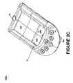
- FIG. 2Cis another exemplary computer system embodiment
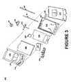
- FIG. 3is an exploded view of the components of the exemplary palmtop computer system of FIG. 2A and FIG. 2C .
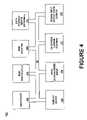
- FIG. 4is a logical block diagram of the exemplary palmtop computer system in accordance with an embodiment of the present invention.
- FIG. 5is a front view of the exemplary computer system that can be used within the display screen of the present invention.
- FIG. 6Ais an exemplary communication network in which the exemplary palmtop computer can be used.
- FIG. 6Bis a perspective view of a cradle device for connecting the exemplary palmtop computer system to other systems via a communication interface.
- FIG. 7illustrates a display screen in accordance with one embodiment of the present invention including a border pixel region and a frame buffer pixel region.
- FIG. 8is a block diagram of the display unit in accordance with one embodiment of the present invention.
- FIG. 9Ais a diagram of a dummy pixel of the border pixel region in accordance with an embodiment of the present invention.
- FIG. 9Bis a diagram of an active pixel of the frame buffer pixel region in accordance with an embodiment of the present invention.
- FIG. 10illustrates the pixel architecture of the display matrix of one embodiment of the present invention including the border pixel region and the frame buffer pixel region.
- FIG. 11Ais a cross sectional view of the display matrix including a cross sectional view of the pixel border in accordance with an embodiment of the present invention.
- FIG. 11Bis a cross sectional view of a reflective display matrix including a cross sectional view of the pixel border in accordance with an embodiment of the present invention.
- FIG. 12is an exemplary display using the display unit with pixel border in accordance with one embodiment of the present invention and having an edge displayed character in a video format in which the character pixels are of the same or similar color as the edge of the display panel.
- FIG. 2Ais a perspective illustration of the top face 100 a of one embodiment of a palmtop computer system that can be used in implementation of the present invention.
- the top face 100 acontains the novel display screen 105 surrounded by a bezel or cover.
- a removable stylus 80is also shown.
- the novel display screen 105contains a transparent touch screen (digitizer) able to register contact between the screen and the tip of the stylus 80 .
- the novel display screen 105is described in more detail further below.
- the stylus 80can be of any material to make contact with the screen 105 . As shown in FIG. 2A , the stylus 80 is inserted into a receiving slot or rail 350 . Slot or rail 350 acts to hold the stylus when the computer system is not in use. Slot or rail 350 may contain switching devices for automatically powering down and automatically powering up computer system based on the position of the stylus 80 .
- the top face 100 aalso contains one or more dedicated and/or programmable buttons 75 for selecting information and causing the computer system to implement functions.
- the on/off button 95is also shown.
- FIG. 2Aalso illustrates a handwriting recognition pad or “digitizer” containing two regions 106 a and 106 b .
- Region 106 ais for the drawing of alpha characters therein for automatic recognition (and generally not used for recognizing numeric characters) and region 106 b is for the drawing of numeric characters therein for automatic recognition (and generally not used for recognizing numeric characters).
- the stylus 80is used for stroking a character within one of the regions 106 a and 106 b .
- the stroke informationis then fed to an internal processor for automatic character recognition. Once characters are recognized, they are typically displayed on the screen 105 for verification and/or modification.
- the digitizer 160records both the (x, y) coordinate value of the current location of the stylus and also simultaneously records the pressure that the stylus exerts on the face of the digitizer pad.
- the coordinate values (spatial information) pressure dataare then output on separate channels for sampling by the processor 101 ( FIG. 5 ). In one implementation, there are roughly 256 different discrete levels of pressure that can be detected by the digitizer 106 . Since the digitizer's channels are sampled serially by the processor, the stroke spatial data are sampled “pseudo” simultaneously with the associated pressure data. The sampled data is then stored in a memory by the processor 101 ( FIG. 5 ) for later analysis.
- FIG. 2Billustrates the bottom side 100 b of one embodiment of the palmtop computer system.
- An optional extendible antenna 85is shown and also a battery storage compartment door 90 is shown.
- a communication interface 108is also shown.
- the serial communication interface 108is a serial communication port, but could also alternatively be of any of a number of well known communication standards and protocols, e.g., parallel, SCSI, Firewire (IEEE 1394), Ethernet, etc.
- FIG. 2Bis also shown the stylus receiving slot or rail 350 .
- FIG. 2Cillustrates a front perspective view of another implementation of the palmtop computer system 100 c .
- the flat central areais composed of the novel display screen area 105 and a thin silk screen layer material portion 84 .
- the silk screen layer material portion 84is opaque and may contain icons, buttons, images, etc., graphically printed thereon in addition to regions 106 a 106 b .
- the novel display screen area 105 and portion 84are disposed over a digitizer.
- FIG. 3is an exploded view of the exemplary palmtop computer system 100 in accordance with one implementation of the present invention.
- System 100contains a front cover 210 having an outline of region 106 and holes 75 a for receiving buttons 75 b .
- the novel flat panel display 105(both liquid crystal display and touch screen in one embodiment) fits into front cover 210 . Any of a number of display technologies can be used, e.g., LCD, FED, plasma, etc., for the flat panel display 105 and having the further details as described below.
- the display 105is a flat panel multi-mode display capable of both monochrome and color display modes.
- the touch screencan be a digitizer.
- a battery 215provides electrical power. Replaceable cells or rechargeable batteries can be used.
- Well known electronics coupled to the battery 215can detect the energy level of the battery 215 .
- This informationcan be sampled by the computer system 110 ( FIG. 5 ) using well known techniques.
- the digitizer of FIG. 3can be implemented using well known devices, for instance, using the ADS-7846 device by Burr-Brown that provides separate channels for spatial stroke information and pressure information.
- An optional contrast adjustment (potentiometer) 220is also shown.
- On/off button 95is shown along with an infrared emitter and detector device 64 .
- a flex circuit 230is shown along with a PC board 225 containing electronics and logic (e.g., memory, communication bus, processor, etc.) for implementing computer system functionality.
- the digitizer padis also included in PC board 225 .
- a midframe 235is shown along with stylus 80 .
- Position adjustable antenna 85is shown. The midframe 235 contains the stylus receiving slot or rail 350 .
- a radio receiver/transmitter device 240is also shown between the midframe and the rear cover 245 of FIG. 3 .
- the receiver/transmitter device 240is coupled to the antenna 85 and also coupled to communicate with the PC board 225 .
- the Mobitex wireless communication systemis used to provide two way communication between system 100 and other networked computers and/or the Internet via a proxy server.
- TCP protocolcan be used.
- FIG. 4illustrates circuitry of computer system 100 , some of which can be implemented on PC board 225 .
- Computer system 100includes an address/data bus 99 for communicating information, a central processor 101 coupled with the bus 99 for processing information and instructions, a volatile memory 102 (e.g., random access memory RAM) coupled with the bus 99 for storing information and instructions for the central processor 101 and a non-volatile memory 103 (e.g., read only memory ROM) coupled with the bus 99 for storing static information and instructions for the processor 101 .
- Computer system 100also includes an optional data storage device 104 (e.g., memory stick) coupled with the bus 99 for storing information and instructions. Device 104 can be removable.
- system 100also contains the novel display device 105 in accordance with the present invention which is coupled to the bus 99 for displaying information to the computer user.
- PC board 225can contain the processor 101 , the bus 99 , the ROM 103 and the RAM 102 .
- an alphanumeric input device 106which in one implementation is a handwriting recognition pad (“digitizer”) having regions 106 a and 106 b ( FIG. 2A ), for instance.
- Device 106can communicate information (spatial data and pressure data) and command selections to the central processor 101 .
- System 100also includes an optional-cursor control or directing device 107 coupled to the bus for communicating user input information and command selections to the central processor 101 .
- device 107is a touch screen device incorporated with screen 105 . Device 107 is capable of registering a position on the screen 105 where the stylus makes contact and the pressure of the contact.
- the display device 105 utilized with the computer system 100is described in more detail below and may be a liquid crystal device, cathode ray tube (CRT), field emission device (FED, also called flat panel CRT) or other display device suitable for creating graphic images and alphanumeric characters recognizable to the user.
- CTRcathode ray tube
- FEDfield emission device
- flat panel CRTflat panel CRT
- Signal communication device 108also coupled to bus 99 , can be a serial port for communicating with the cradle 60 .
- Device 108can also include an infrared communication port.
- FIG. 5is a front view of the exemplary palmtop computer system 100 having an exemplary display within screen 105 .
- the exemplary displaycontains one or more graphical user-interface elements including a menu bar and selectable on-screen buttons 410 . Buttons on screen 105 can be selected by the user directly tapping on the screen location of the button with stylus 80 as is well known.
- two regions of digitizer 106 a and 106 bare also shown. Region 106 a is for receiving user stroke data (and pressure data) for alphabet characters, and typically not numeric characters, and region 106 b is for receiving user stroke data (and pressure data) for numeric data, and typically not for alphabetic characters.
- Physical buttons 75are also shown. Although different regions are shown for alphabetic and numeric characters, the device is also operable within a single region that recognizes both alphabetic and numeric characters.
- the digitizer region 106 a and 106 bare separate from the display screen 105 and therefore does not consume any display area.
- FIG. 6Aillustrates a communication system 50 that can be used in conjunction with the palmtop computer system 100 .
- System 50is exemplary and comprises a host computer system 56 which can either be a desktop unit as shown, or, alternatively, can be a laptop system 58 .
- one or more host computer systemscan be used within system 50 .
- Host computer systems 58 and 56are shown connected to a communication bus 54 , which in one embodiment can be a serial communication bus, but could be of any of a number of well known designs, e.g., a parallel bus, Ethernet Local Area Network (LAN), etc.
- bus 54can provide communication with the Internet 52 using a number of well known protocols.
- bus 54is also coupled to a cradle 60 for receiving and initiating communication with a palm top (“palm-sized”) portable computer system 100 of the present invention.
- Cradle 60provides an electrical and mechanical communication interface between bus 54 (and anything coupled to bus 54 ) and the computer system 100 for two way communications.
- Computer system 100also contains a wireless infrared communication mechanism 64 for sending and receiving information from other devices.
- FIG. 6Bis a perspective illustration of one embodiment of the cradle 60 for receiving the palmtop computer system 100 .
- Cradle 60contains a mechanical and electrical interface 260 for interfacing with serial connection 108 ( FIG. 2B ) of computer system 100 when system 100 is slid into the cradle 60 in an upright position. Once inserted, button 270 can be pressed to initiate two way communication between system 100 and other computer systems coupled to serial communication 265 .
- FIG. 7illustrates a front view of the display screen in accordance with an embodiment of the present invention.
- the display screencontains two different display regions.
- Region 314is the frame buffer pixel region and contains a matrix of pixels oriented in m rows and n columns according to a variety of display dimensions and formats.
- Region 314generates an image that is a representation of data stored in a frame buffer memory (also called video memory) of computer system 100 .
- region 314can have any dimensions, in one embodiment it includes the dimensions of 160 pixels by 160 pixels.
- the computer systeme.g., the operating system, controls the information that is stored into the frame buffer memory and thereby controls the pixels of region 314 .
- Surrounding region 314 of FIG. 7is a novel pixel border region 312 in accordance with the present invention and having a predetermined pixel width, x.
- the pixels of the pixel border region 312are called “dummy” pixels because they do not have a controllable element therein.
- the widthis arbitrary, in one embodiment the width is two pixels.
- the pixel border region 312 of the present inventionis not controlled by the frame buffer memory and is useful for giving contrast improvement for the viewability of edge located characters.
- the pixels of the pixel border 312are generally displayed white to match the background pixel color.
- the pixel border 312is useful for giving contrast improvement for characters displayed along the edges, e.g., upper, lower, right and left, of region 314 .
- FIG. 8illustrates a logical diagram of the components of the novel display unit 105 in accordance with an embodiment of the present invention.
- Frame buffer memory 320contains a bitmapped image for display. This frame buffer is read, periodically, by a display controller 322 .
- the display controller 322is well known.
- Display controller 322is either coupled directly to a display driver 326 or to a timing generator 324 .
- Controller 322generates well known timing signals, such as vertical and horizontal synchronization signals, as well as clocking signals; all required to properly propagate image data into the display drivers 326 .
- the timing generator 324is sometimes needed to convert the signals from the controller according to the requirements of the drivers.
- the display drivers 326are coupled to active transistors within the display matrix 310 .
- the display matrix 310generates images by the modulation of light by discrete pixel elements.
- the display matrix 310can be of liquid crystal display (LCD) technology but could also be of any active display technology, such as field emission display (FED) technology or other flat panel display technologies.
- LCDliquid crystal display
- FEDfield emission display
- display matrix 310is coupled to display drivers 326 , it is appreciated that region 312 is not coupled to display drivers because it contains no active elements.
- FIG. 9Aillustrates an example dummy pixel 312 i of the pixel border region 312 of the present invention.
- the display matrix 310is an LCD device constructed using thin film transistor (TFT) technology.
- the dummy pixelis like a conventional pixel of the frame buffer pixel region 314 except the dummy pixel 312 i does not contain an active element, as indicated by the darkened diamond 340 .
- the active elementcan be any number of display elements, including a transistor, a series of diodes or a single diode. Therefore, the dummy pixels are not controlled by the frame buffer memory and are not coupled electrically to the display driver circuits 326 ( FIG. 8 ).
- the displayis a color display and therefore the dummy pixel 312 i is comprised of three sub-dummy-pixels including a red sub-dummy-pixel 342 a , a green sub-dummy-pixel 342 b and a blue sub-dummy-pixel 342 c .
- Each sub-dummy-pixel 342 a - 342 ccontains a respective color filter. It is appreciated that by not containing an active transistor therein, each of the sub-dummy-pixels 342 a - 342 c of the dummy pixel 312 i remain fixed and open thereby allowing light to pass there through creating a white image for the dummy pixel 312 i .
- Each sub-dummy-pixelcontains a respective color filter.
- FIG. 9Billustrates a pixel 3141 of the frame buffer pixel region 314 .
- the displayis color and therefore pixel 3141 contains a red subpixel 352 a , a green subpixel 352 b and a blue subpixel 352 c .
- Each subpixelcontains a respective active element 350 , e.g., transistor, that is controlled by the frame buffer memory, e.g., each transistor 350 is coupled to the display driver circuits 326 ( FIG. 8 ).
- each subpixel 352also contains a respective color filter.
- the left hand side of the pixel border 312is shown partially with the upper and lower corners displayed.
- dummy transistorsare darkened.
- Two columns of dummy pixelsare shown 360 along the left side edge.
- two rows of dummy pixels 362are also shown and also on the bottom.
- the dummy pixels 312 i of the border region 312surround the frame buffer display region 314 , which contains an array of m rows and n columns of pixels, some of which are shown as 314 i .
- the LCD glasshas a color filter pattern of 164 ⁇ 164 pixels which allow light through from a back light element ( FIG. 11 ).
- the LCD glasshas transistors placed on only the interior 160 ⁇ 160 pixels (region 314 ) which are addressed by the frame buffer memory. In this case, the pixel border 312 remains lit all the time thereby providing a white border.
- FIG. 11Aillustrates a cross section of the display matrix 310 in accordance with one embodiment of the present invention.
- a backlighting element 570e.g., a cold cathode fluorescent (CCF) tube or other lighting device
- CCFcold cathode fluorescent
- An active transistor LCD layer 530is also shown.
- the active transistor layer 530maps to region 314 and may control m rows and n columns of pixels.
- Region 540 and region 550correspond to the dummy pixel border 312 and therefore do not contain any transistors thereby always allowing light to pass there through.
- a color filter pattern 520is also shown.
- the color filter pattern 520is a matrix of (m+2x) by (n+2x) pixels.
- a front polarizer layer 510is provided.
- FIG. 11Billustrates a cross section of a reflective display matrix 610 in accordance with one embodiment of the present invention.
- a reflective thin film transistor layer 620is used.
- Layer 620maps to region 314 and may control m rows and n columns of pixels.
- Region 640 and region 630correspond to the dummy pixel border 312 and therefore do not contain any transistors thereby always allowing light to pass there through.
- An optional frontlight layer 650can be used and a front polarizer 510 is shown along with a rear polarizer 560 .
- the color filter pattern 520is a matrix of (m+2x) by (n+2x) pixels.
- the pixels 380 of the edge displayed character, “A,”are dark and the background pixels are white in this case, e.g., one exemplary form of a reverse video display format.
- the edge region 28 of the display panelis dark, e.g., the same or similar color as the pixels 380 of the character.
- the border pixels 312 of the present inventionare also white.
- the total number of pixels in the display 310are (m+2x) by (n+2x).
Landscapes
- Physics & Mathematics (AREA)
- Engineering & Computer Science (AREA)
- Chemical & Material Sciences (AREA)
- Crystallography & Structural Chemistry (AREA)
- Nonlinear Science (AREA)
- General Physics & Mathematics (AREA)
- Microelectronics & Electronic Packaging (AREA)
- Mathematical Physics (AREA)
- Optics & Photonics (AREA)
- Computer Hardware Design (AREA)
- Theoretical Computer Science (AREA)
- Control Of Indicators Other Than Cathode Ray Tubes (AREA)
Abstract
Description
Claims (17)
Priority Applications (1)
| Application Number | Priority Date | Filing Date | Title |
|---|---|---|---|
| US11/243,037US7324072B1 (en) | 2000-11-08 | 2005-10-03 | Pixel border for improved viewability of a display device |
Applications Claiming Priority (2)
| Application Number | Priority Date | Filing Date | Title |
|---|---|---|---|
| US09/709,142US6961029B1 (en) | 2000-11-08 | 2000-11-08 | Pixel border for improved viewability of a display device |
| US11/243,037US7324072B1 (en) | 2000-11-08 | 2005-10-03 | Pixel border for improved viewability of a display device |
Related Parent Applications (1)
| Application Number | Title | Priority Date | Filing Date |
|---|---|---|---|
| US09/709,142ContinuationUS6961029B1 (en) | 2000-11-08 | 2000-11-08 | Pixel border for improved viewability of a display device |
Publications (1)
| Publication Number | Publication Date |
|---|---|
| US7324072B1true US7324072B1 (en) | 2008-01-29 |
Family
ID=35150798
Family Applications (3)
| Application Number | Title | Priority Date | Filing Date |
|---|---|---|---|
| US09/709,142Expired - LifetimeUS6961029B1 (en) | 2000-11-08 | 2000-11-08 | Pixel border for improved viewability of a display device |
| US09/724,197Expired - Fee RelatedUS7362338B1 (en) | 2000-11-08 | 2000-11-27 | Controllable pixel border for improved viewability of a display device |
| US11/243,037Expired - Fee RelatedUS7324072B1 (en) | 2000-11-08 | 2005-10-03 | Pixel border for improved viewability of a display device |
Family Applications Before (2)
| Application Number | Title | Priority Date | Filing Date |
|---|---|---|---|
| US09/709,142Expired - LifetimeUS6961029B1 (en) | 2000-11-08 | 2000-11-08 | Pixel border for improved viewability of a display device |
| US09/724,197Expired - Fee RelatedUS7362338B1 (en) | 2000-11-08 | 2000-11-27 | Controllable pixel border for improved viewability of a display device |
Country Status (1)
| Country | Link |
|---|---|
| US (3) | US6961029B1 (en) |
Cited By (5)
| Publication number | Priority date | Publication date | Assignee | Title |
|---|---|---|---|---|
| US20030093469A1 (en)* | 2000-10-16 | 2003-05-15 | Akihiro Ohta | Apparatus control method and device |
| US7890881B1 (en)* | 2005-07-29 | 2011-02-15 | Adobe Systems Incorporated | Systems and methods for a fold preview |
| US20120169578A1 (en)* | 2010-12-29 | 2012-07-05 | Chang-Sin Kim | Display Panel and Display Apparatus Having the Same |
| US20150269742A1 (en)* | 2014-03-21 | 2015-09-24 | Fluke Corporation | Visible light image with edge marking for enhancing ir imagery |
| US10152811B2 (en) | 2015-08-27 | 2018-12-11 | Fluke Corporation | Edge enhancement for thermal-visible combined images and cameras |
Families Citing this family (40)
| Publication number | Priority date | Publication date | Assignee | Title |
|---|---|---|---|---|
| US6961029B1 (en)* | 2000-11-08 | 2005-11-01 | Palm, Inc. | Pixel border for improved viewability of a display device |
| US7724270B1 (en) | 2000-11-08 | 2010-05-25 | Palm, Inc. | Apparatus and methods to achieve a variable color pixel border on a negative mode screen with a passive matrix drive |
| JP3628997B2 (en)* | 2000-11-27 | 2005-03-16 | セイコーエプソン株式会社 | Method for manufacturing organic electroluminescence device |
| US7158675B2 (en)* | 2002-05-14 | 2007-01-02 | Microsoft Corporation | Interfacing with ink |
| US7925987B2 (en)* | 2002-05-14 | 2011-04-12 | Microsoft Corporation | Entry and editing of electronic ink |
| US20030214553A1 (en)* | 2002-05-14 | 2003-11-20 | Microsoft Corporation | Ink regions in an overlay control |
| US8166388B2 (en) | 2002-05-14 | 2012-04-24 | Microsoft Corporation | Overlaying electronic ink |
| KR100878790B1 (en) | 2002-09-05 | 2009-01-14 | 삼성전자주식회사 | Active matrix image display device and image display method using same |
| JP4046011B2 (en)* | 2003-05-29 | 2008-02-13 | 松下電器産業株式会社 | Flat panel display |
| US8717301B2 (en) | 2005-08-01 | 2014-05-06 | Sony Corporation | Information processing apparatus and method, and program |
| JP5358865B2 (en)* | 2005-06-23 | 2013-12-04 | ソニー株式会社 | Display terminal device |
| US8920343B2 (en) | 2006-03-23 | 2014-12-30 | Michael Edward Sabatino | Apparatus for acquiring and processing of physiological auditory signals |
| WO2008005629A2 (en)* | 2006-05-26 | 2008-01-10 | Riverbed Technology, Inc. | Throttling of predictive acks in an accelerated network communication system |
| US20080143876A1 (en)* | 2006-08-31 | 2008-06-19 | James Kouramanis | Video stream timing detection |
| GB0702350D0 (en) | 2007-02-07 | 2007-03-21 | Plastic Logic Ltd | Electronic reading devices |
| GB0702347D0 (en)* | 2007-02-07 | 2007-03-21 | Plastic Logic Ltd | Electronic document reading devices |
| GB0702349D0 (en)* | 2007-02-07 | 2007-03-21 | Plastic Logic Ltd | Electronic document readers and reading devices |
| GB2454032A (en) | 2007-10-24 | 2009-04-29 | Plastic Logic Ltd | Edgeless document viewer |
| US20090150435A1 (en)* | 2007-12-08 | 2009-06-11 | International Business Machines Corporation | Dynamic updating of personal web page |
| GB2458106B (en) | 2008-03-03 | 2012-07-18 | Plastic Logic Ltd | Electronic document reader system |
| US8587758B2 (en)* | 2009-02-13 | 2013-11-19 | Apple Inc. | Electrodes for use in displays |
| US8531408B2 (en)* | 2009-02-13 | 2013-09-10 | Apple Inc. | Pseudo multi-domain design for improved viewing angle and color shift |
| US8294647B2 (en)* | 2009-02-13 | 2012-10-23 | Apple Inc. | LCD pixel design varying by color |
| US8390553B2 (en)* | 2009-02-13 | 2013-03-05 | Apple Inc. | Advanced pixel design for optimized driving |
| US9612489B2 (en)* | 2009-02-13 | 2017-04-04 | Apple Inc. | Placement and shape of electrodes for use in displays |
| US8345177B2 (en)* | 2009-02-13 | 2013-01-01 | Shih Chang Chang | Via design for use in displays |
| US8558978B2 (en)* | 2009-02-13 | 2013-10-15 | Apple Inc. | LCD panel with index-matching passivation layers |
| US20100208179A1 (en)* | 2009-02-13 | 2010-08-19 | Apple Inc. | Pixel Black Mask Design and Formation Technique |
| US8633879B2 (en) | 2009-02-13 | 2014-01-21 | Apple Inc. | Undulating electrodes for improved viewing angle and color shift |
| US8111232B2 (en)* | 2009-03-27 | 2012-02-07 | Apple Inc. | LCD electrode arrangement |
| US8294850B2 (en)* | 2009-03-31 | 2012-10-23 | Apple Inc. | LCD panel having improved response |
| KR101965207B1 (en)* | 2012-03-27 | 2019-04-05 | 삼성디스플레이 주식회사 | Display apparatus |
| TWI449012B (en) | 2012-04-20 | 2014-08-11 | E Ink Holdings Inc | Display apparatus and display method thereof |
| JP2015132862A (en)* | 2012-04-27 | 2015-07-23 | シャープ株式会社 | Touch panel-attached display device |
| KR102413473B1 (en)* | 2015-10-01 | 2022-06-28 | 삼성디스플레이 주식회사 | Method of display apparatus |
| US10547846B2 (en)* | 2017-04-17 | 2020-01-28 | Intel Corporation | Encoding 3D rendered images by tagging objects |
| US10602139B2 (en)* | 2017-12-27 | 2020-03-24 | Omnivision Technologies, Inc. | Embedded multimedia systems with adaptive rate control for power efficient video streaming |
| CN109671760A (en)* | 2018-12-18 | 2019-04-23 | 武汉华星光电半导体显示技术有限公司 | A kind of active matrix organic LED panel |
| KR102652983B1 (en) | 2019-06-04 | 2024-04-01 | 삼성디스플레이 주식회사 | Display apparatus and method of driving display panel using the same |
| TWI768317B (en)* | 2020-04-01 | 2022-06-21 | 緯創資通股份有限公司 | Display device and display method thereof |
Citations (36)
| Publication number | Priority date | Publication date | Assignee | Title |
|---|---|---|---|---|
| US4620289A (en) | 1983-04-25 | 1986-10-28 | Texas Instruments Incorporated | Video display system |
| US4731742A (en) | 1984-03-16 | 1988-03-15 | Ascii Corporation | Video display control system |
| EP0283235A2 (en) | 1987-03-14 | 1988-09-21 | Sharp Kabushiki Kaisha | Liquid crystal display device |
| US4814756A (en) | 1980-12-12 | 1989-03-21 | Texas Instruments Incorporated | Video display control system having improved storage of alphanumeric and graphic display data |
| GB2214342A (en) | 1988-01-19 | 1989-08-31 | Mitsubishi Electric Corp | Liquid crystal display apparatus |
| EP0394814A1 (en) | 1989-04-24 | 1990-10-31 | Asulab S.A. | Improved electro-optical display cell |
| US5038297A (en) | 1988-09-13 | 1991-08-06 | Silicon Graphics, Inc. | Method and apparatus for clearing a region of Z-buffer |
| US5086295A (en) | 1988-01-12 | 1992-02-04 | Boettcher Eric R | Apparatus for increasing color and spatial resolutions of a raster graphics system |
| US5355443A (en) | 1990-06-04 | 1994-10-11 | University Of Washington | Image computing system |
| US5513028A (en)* | 1992-02-27 | 1996-04-30 | Canon Kabushiki Kaisha | Liquid crystal display with display area having same height as peripheral portion thereof |
| US5559529A (en) | 1992-02-26 | 1996-09-24 | Rockwell International | Discrete media display device and method for efficiently drawing lines on same |
| US5657043A (en) | 1994-04-18 | 1997-08-12 | Matsushita Electric Industrial Co., Ltd. | Driving apparatus for liquid crystal display |
| US5719648A (en)* | 1995-07-14 | 1998-02-17 | Sharp Kabushiki Kaisha | Liquid crystal display apparatus and method for producing the same with electrodes for producing a reference signal outside display area |
| US5754186A (en) | 1993-05-10 | 1998-05-19 | Apple Computer, Inc. | Method and apparatus for blending images |
| US5784132A (en)* | 1994-10-19 | 1998-07-21 | Sony Corporation | Display device |
| US5805149A (en) | 1991-10-28 | 1998-09-08 | Canon Kabushiki Kaisha | Display control device and display apparatus with display control device |
| US5825343A (en) | 1995-01-11 | 1998-10-20 | Samsung Electronics Co., Ltd. | Driving device and driving method for a thin film transistor liquid crystal display |
| US5838334A (en) | 1994-11-16 | 1998-11-17 | Dye; Thomas A. | Memory and graphics controller which performs pointer-based display list video refresh operations |
| US5844539A (en) | 1996-02-02 | 1998-12-01 | Sony Corporation | Image display system |
| US6018331A (en) | 1996-12-04 | 2000-01-25 | Nec Corporation | Frame display control in an image display having a liquid crystal display panel |
| US6064359A (en) | 1997-07-09 | 2000-05-16 | Seiko Epson Corporation | Frame rate modulation for liquid crystal display (LCD) |
| US6100858A (en) | 1997-09-30 | 2000-08-08 | Infineon Technologies North America Corp. | Alphanumeric display with 21-dot matrix format |
| US6140992A (en) | 1994-01-11 | 2000-10-31 | Canon Kabushiki Kaisha | Display control system which prevents transmission of the horizontal synchronizing signal for a predetermined period when the display state has changed |
| US6181313B1 (en) | 1997-01-30 | 2001-01-30 | Hitachi, Ltd. | Liquid crystal display controller and liquid crystal display device |
| US6195078B1 (en) | 1996-08-21 | 2001-02-27 | Thomson Licensing S.A. | Parallel mode on-screen display system |
| US6204895B1 (en)* | 1997-09-30 | 2001-03-20 | Kabushiki Kaisha Toshiba | Display panel associated with light collecting plate and position adjusting method using microlenses for the display panel |
| US6288704B1 (en) | 1999-06-08 | 2001-09-11 | Vega, Vista, Inc. | Motion detection and tracking system to control navigation and display of object viewers |
| US6323834B1 (en) | 1998-10-08 | 2001-11-27 | International Business Machines Corporation | Micromechanical displays and fabrication method |
| US6323849B1 (en) | 1999-01-22 | 2001-11-27 | Motorola, Inc. | Display module with reduced power consumption |
| US6476821B2 (en) | 1997-01-31 | 2002-11-05 | Hitachi, Ltd. | Image displaying system and information processing apparatus |
| US6535188B1 (en) | 1998-07-08 | 2003-03-18 | Kabushiki Kaisha Toshiba | Liquid crystal display device |
| US6577291B2 (en)* | 1998-10-07 | 2003-06-10 | Microsoft Corporation | Gray scale and color display methods and apparatus |
| US6590592B1 (en) | 1999-04-23 | 2003-07-08 | Xsides Corporation | Parallel interface |
| US6597373B1 (en) | 2000-01-07 | 2003-07-22 | Intel Corporation | System and method of aligning images for display devices |
| US6831662B1 (en) | 2000-11-08 | 2004-12-14 | Palmone, Inc. | Apparatus and methods to achieve a variable color pixel border on a negative mode screen with a passive matrix drive |
| US6961029B1 (en)* | 2000-11-08 | 2005-11-01 | Palm, Inc. | Pixel border for improved viewability of a display device |
- 2000
- 2000-11-08USUS09/709,142patent/US6961029B1/ennot_activeExpired - Lifetime
- 2000-11-27USUS09/724,197patent/US7362338B1/ennot_activeExpired - Fee Related
- 2005
- 2005-10-03USUS11/243,037patent/US7324072B1/ennot_activeExpired - Fee Related
Patent Citations (37)
| Publication number | Priority date | Publication date | Assignee | Title |
|---|---|---|---|---|
| US4814756A (en) | 1980-12-12 | 1989-03-21 | Texas Instruments Incorporated | Video display control system having improved storage of alphanumeric and graphic display data |
| US4620289A (en) | 1983-04-25 | 1986-10-28 | Texas Instruments Incorporated | Video display system |
| US4731742A (en) | 1984-03-16 | 1988-03-15 | Ascii Corporation | Video display control system |
| EP0283235A2 (en) | 1987-03-14 | 1988-09-21 | Sharp Kabushiki Kaisha | Liquid crystal display device |
| US4824212A (en) | 1987-03-14 | 1989-04-25 | Sharp Kabushiki Kaisha | Liquid crystal display device having separate driving circuits for display and non-display regions |
| US5086295A (en) | 1988-01-12 | 1992-02-04 | Boettcher Eric R | Apparatus for increasing color and spatial resolutions of a raster graphics system |
| GB2214342A (en) | 1988-01-19 | 1989-08-31 | Mitsubishi Electric Corp | Liquid crystal display apparatus |
| US5038297A (en) | 1988-09-13 | 1991-08-06 | Silicon Graphics, Inc. | Method and apparatus for clearing a region of Z-buffer |
| EP0394814A1 (en) | 1989-04-24 | 1990-10-31 | Asulab S.A. | Improved electro-optical display cell |
| US5355443A (en) | 1990-06-04 | 1994-10-11 | University Of Washington | Image computing system |
| US5805149A (en) | 1991-10-28 | 1998-09-08 | Canon Kabushiki Kaisha | Display control device and display apparatus with display control device |
| US5559529A (en) | 1992-02-26 | 1996-09-24 | Rockwell International | Discrete media display device and method for efficiently drawing lines on same |
| US5513028A (en)* | 1992-02-27 | 1996-04-30 | Canon Kabushiki Kaisha | Liquid crystal display with display area having same height as peripheral portion thereof |
| US5754186A (en) | 1993-05-10 | 1998-05-19 | Apple Computer, Inc. | Method and apparatus for blending images |
| US6140992A (en) | 1994-01-11 | 2000-10-31 | Canon Kabushiki Kaisha | Display control system which prevents transmission of the horizontal synchronizing signal for a predetermined period when the display state has changed |
| US5657043A (en) | 1994-04-18 | 1997-08-12 | Matsushita Electric Industrial Co., Ltd. | Driving apparatus for liquid crystal display |
| US5784132A (en)* | 1994-10-19 | 1998-07-21 | Sony Corporation | Display device |
| US5838334A (en) | 1994-11-16 | 1998-11-17 | Dye; Thomas A. | Memory and graphics controller which performs pointer-based display list video refresh operations |
| US5825343A (en) | 1995-01-11 | 1998-10-20 | Samsung Electronics Co., Ltd. | Driving device and driving method for a thin film transistor liquid crystal display |
| US5719648A (en)* | 1995-07-14 | 1998-02-17 | Sharp Kabushiki Kaisha | Liquid crystal display apparatus and method for producing the same with electrodes for producing a reference signal outside display area |
| US5844539A (en) | 1996-02-02 | 1998-12-01 | Sony Corporation | Image display system |
| US6195078B1 (en) | 1996-08-21 | 2001-02-27 | Thomson Licensing S.A. | Parallel mode on-screen display system |
| US6018331A (en) | 1996-12-04 | 2000-01-25 | Nec Corporation | Frame display control in an image display having a liquid crystal display panel |
| US6181313B1 (en) | 1997-01-30 | 2001-01-30 | Hitachi, Ltd. | Liquid crystal display controller and liquid crystal display device |
| US6476821B2 (en) | 1997-01-31 | 2002-11-05 | Hitachi, Ltd. | Image displaying system and information processing apparatus |
| US6064359A (en) | 1997-07-09 | 2000-05-16 | Seiko Epson Corporation | Frame rate modulation for liquid crystal display (LCD) |
| US6100858A (en) | 1997-09-30 | 2000-08-08 | Infineon Technologies North America Corp. | Alphanumeric display with 21-dot matrix format |
| US6204895B1 (en)* | 1997-09-30 | 2001-03-20 | Kabushiki Kaisha Toshiba | Display panel associated with light collecting plate and position adjusting method using microlenses for the display panel |
| US6535188B1 (en) | 1998-07-08 | 2003-03-18 | Kabushiki Kaisha Toshiba | Liquid crystal display device |
| US6577291B2 (en)* | 1998-10-07 | 2003-06-10 | Microsoft Corporation | Gray scale and color display methods and apparatus |
| US6323834B1 (en) | 1998-10-08 | 2001-11-27 | International Business Machines Corporation | Micromechanical displays and fabrication method |
| US6323849B1 (en) | 1999-01-22 | 2001-11-27 | Motorola, Inc. | Display module with reduced power consumption |
| US6590592B1 (en) | 1999-04-23 | 2003-07-08 | Xsides Corporation | Parallel interface |
| US6288704B1 (en) | 1999-06-08 | 2001-09-11 | Vega, Vista, Inc. | Motion detection and tracking system to control navigation and display of object viewers |
| US6597373B1 (en) | 2000-01-07 | 2003-07-22 | Intel Corporation | System and method of aligning images for display devices |
| US6831662B1 (en) | 2000-11-08 | 2004-12-14 | Palmone, Inc. | Apparatus and methods to achieve a variable color pixel border on a negative mode screen with a passive matrix drive |
| US6961029B1 (en)* | 2000-11-08 | 2005-11-01 | Palm, Inc. | Pixel border for improved viewability of a display device |
Cited By (11)
| Publication number | Priority date | Publication date | Assignee | Title |
|---|---|---|---|---|
| US20030093469A1 (en)* | 2000-10-16 | 2003-05-15 | Akihiro Ohta | Apparatus control method and device |
| US7568159B2 (en)* | 2000-10-16 | 2009-07-28 | Sony Corporation | Apparatus control method and system |
| US7890881B1 (en)* | 2005-07-29 | 2011-02-15 | Adobe Systems Incorporated | Systems and methods for a fold preview |
| US20120169578A1 (en)* | 2010-12-29 | 2012-07-05 | Chang-Sin Kim | Display Panel and Display Apparatus Having the Same |
| US8963818B2 (en)* | 2010-12-29 | 2015-02-24 | Samsung Display Co., Ltd. | Display panel and display apparatus having the same |
| US20150269742A1 (en)* | 2014-03-21 | 2015-09-24 | Fluke Corporation | Visible light image with edge marking for enhancing ir imagery |
| US9990730B2 (en)* | 2014-03-21 | 2018-06-05 | Fluke Corporation | Visible light image with edge marking for enhancing IR imagery |
| US10366496B2 (en) | 2014-03-21 | 2019-07-30 | Fluke Corporation | Visible light image with edge marking for enhancing IR imagery |
| US10726559B2 (en) | 2014-03-21 | 2020-07-28 | Fluke Corporation | Visible light image with edge marking for enhancing IR imagery |
| US10152811B2 (en) | 2015-08-27 | 2018-12-11 | Fluke Corporation | Edge enhancement for thermal-visible combined images and cameras |
| US10872448B2 (en) | 2015-08-27 | 2020-12-22 | Fluke Corporation | Edge enhancement for thermal-visible combined images and cameras |
Also Published As
| Publication number | Publication date |
|---|---|
| US6961029B1 (en) | 2005-11-01 |
| US7362338B1 (en) | 2008-04-22 |
Similar Documents
| Publication | Publication Date | Title |
|---|---|---|
| US7324072B1 (en) | Pixel border for improved viewability of a display device | |
| US7425970B1 (en) | Controllable pixel border for a negative mode passive matrix display device | |
| US7002569B1 (en) | Method and apparatus for user selectable display mode for intelligently enhancing battery life | |
| US7289083B1 (en) | Multi-sided display for portable computer | |
| US7552349B2 (en) | User configurable power conservation through LCD display screen reduction | |
| US20080150901A1 (en) | Integrated Liquid Crystal Display And Touchscreen For An Electronic Device | |
| TW574524B (en) | Electronic apparatus provided with organic electroluminescent device | |
| US6232937B1 (en) | Low power active display system | |
| CN101273396B (en) | Flat-panel display with hybrid imaging technology | |
| EP1936479A1 (en) | Integrated Liquid Crystal Display and Touchscreen for an Electronic Device | |
| EP3629321B1 (en) | Display structure, display panel and display device | |
| US6476784B2 (en) | Portable display system with memory card reader | |
| US8237718B2 (en) | Apparatus and methods to achieve a variable color pixel border on a negative mode screen with a passive matrix drive | |
| JP2003315764A (en) | Liquid crystal display | |
| JP2005182005A (en) | Display device and electronic equipment | |
| US6552704B2 (en) | Color display with thin gap liquid crystal | |
| JP4693222B2 (en) | Portable electronic device | |
| JP2008209711A (en) | Electronic paper | |
| Oyama et al. | Smaller and bigger displays | |
| US8525773B2 (en) | Apparatus for control liquid crystal timing | |
| US20030034942A1 (en) | Electronic device with a display and method for controlling a display | |
| US7138964B2 (en) | Mobile unit with dual panel display | |
| JP2001237934A (en) | Electronic apparatus having display panel and portable radio communication device | |
| KR20230158762A (en) | Image display apparatus and method thereof | |
| JP2017054134A (en) | Information terminal |
Legal Events
| Date | Code | Title | Description |
|---|---|---|---|
| FEPP | Fee payment procedure | Free format text:PAYOR NUMBER ASSIGNED (ORIGINAL EVENT CODE: ASPN); ENTITY STATUS OF PATENT OWNER: LARGE ENTITY | |
| AS | Assignment | Owner name:JPMORGAN CHASE BANK, N.A., NEW YORK Free format text:SECURITY AGREEMENT;ASSIGNOR:PALM, INC.;REEL/FRAME:020341/0285 Effective date:20071219 Owner name:JPMORGAN CHASE BANK, N.A.,NEW YORK Free format text:SECURITY AGREEMENT;ASSIGNOR:PALM, INC.;REEL/FRAME:020341/0285 Effective date:20071219 | |
| STCF | Information on status: patent grant | Free format text:PATENTED CASE | |
| AS | Assignment | Owner name:JPMORGAN CHASE BANK, N.A., NEW YORK Free format text:SECURITY AGREEMENT;ASSIGNOR:PALM, INC.;REEL/FRAME:021158/0380 Effective date:20080414 | |
| AS | Assignment | Owner name:PALM, INC., CALIFORNIA Free format text:RELEASE BY SECURED PARTY;ASSIGNOR:JPMORGAN CHASE BANK, N.A., AS ADMINISTRATIVE AGENT;REEL/FRAME:024630/0474 Effective date:20100701 | |
| AS | Assignment | Owner name:HEWLETT-PACKARD DEVELOPMENT COMPANY, L.P., TEXAS Free format text:ASSIGNMENT OF ASSIGNORS INTEREST;ASSIGNOR:PALM, INC.;REEL/FRAME:025204/0809 Effective date:20101027 | |
| FPAY | Fee payment | Year of fee payment:4 | |
| AS | Assignment | Owner name:PALM, INC., CALIFORNIA Free format text:ASSIGNMENT OF ASSIGNORS INTEREST;ASSIGNOR:HEWLETT-PACKARD DEVELOPMENT COMPANY, L.P.;REEL/FRAME:030341/0459 Effective date:20130430 | |
| AS | Assignment | Owner name:HEWLETT-PACKARD DEVELOPMENT COMPANY, L.P., TEXAS Free format text:ASSIGNMENT OF ASSIGNORS INTEREST;ASSIGNOR:PALM, INC.;REEL/FRAME:031837/0239 Effective date:20131218 Owner name:PALM, INC., CALIFORNIA Free format text:ASSIGNMENT OF ASSIGNORS INTEREST;ASSIGNOR:HEWLETT-PACKARD DEVELOPMENT COMPANY, L.P.;REEL/FRAME:031837/0544 Effective date:20131218 Owner name:HEWLETT-PACKARD DEVELOPMENT COMPANY, L.P., TEXAS Free format text:ASSIGNMENT OF ASSIGNORS INTEREST;ASSIGNOR:PALM, INC.;REEL/FRAME:031837/0659 Effective date:20131218 | |
| AS | Assignment | Owner name:QUALCOMM INCORPORATED, CALIFORNIA Free format text:ASSIGNMENT OF ASSIGNORS INTEREST;ASSIGNORS:HEWLETT-PACKARD COMPANY;HEWLETT-PACKARD DEVELOPMENT COMPANY, L.P.;PALM, INC.;REEL/FRAME:032132/0001 Effective date:20140123 | |
| FPAY | Fee payment | Year of fee payment:8 | |
| FEPP | Fee payment procedure | Free format text:MAINTENANCE FEE REMINDER MAILED (ORIGINAL EVENT CODE: REM.); ENTITY STATUS OF PATENT OWNER: LARGE ENTITY | |
| LAPS | Lapse for failure to pay maintenance fees | Free format text:PATENT EXPIRED FOR FAILURE TO PAY MAINTENANCE FEES (ORIGINAL EVENT CODE: EXP.); ENTITY STATUS OF PATENT OWNER: LARGE ENTITY | |
| STCH | Information on status: patent discontinuation | Free format text:PATENT EXPIRED DUE TO NONPAYMENT OF MAINTENANCE FEES UNDER 37 CFR 1.362 | |
| FP | Lapsed due to failure to pay maintenance fee | Effective date:20200129 |