US7324043B2 - Phase shifters deposited en masse for an electronically scanned antenna - Google Patents
Phase shifters deposited en masse for an electronically scanned antennaDownload PDFInfo
- Publication number
- US7324043B2 US7324043B2US11/219,400US21940005AUS7324043B2US 7324043 B2US7324043 B2US 7324043B2US 21940005 AUS21940005 AUS 21940005AUS 7324043 B2US7324043 B2US 7324043B2
- Authority
- US
- United States
- Prior art keywords
- electrode
- phase shifter
- phase
- radiating element
- antenna
- Prior art date
- Legal status (The legal status is an assumption and is not a legal conclusion. Google has not performed a legal analysis and makes no representation as to the accuracy of the status listed.)
- Active, expires
Links
Images


Classifications
- H—ELECTRICITY
- H01—ELECTRIC ELEMENTS
- H01P—WAVEGUIDES; RESONATORS, LINES, OR OTHER DEVICES OF THE WAVEGUIDE TYPE
- H01P1/00—Auxiliary devices
- H01P1/18—Phase-shifters
- H01P1/181—Phase-shifters using ferroelectric devices
- H—ELECTRICITY
- H01—ELECTRIC ELEMENTS
- H01Q—ANTENNAS, i.e. RADIO AERIALS
- H01Q21/00—Antenna arrays or systems
- H01Q21/0006—Particular feeding systems
- H01Q21/0075—Stripline fed arrays
- H—ELECTRICITY
- H01—ELECTRIC ELEMENTS
- H01Q—ANTENNAS, i.e. RADIO AERIALS
- H01Q21/00—Antenna arrays or systems
- H01Q21/0087—Apparatus or processes specially adapted for manufacturing antenna arrays
- H—ELECTRICITY
- H01—ELECTRIC ELEMENTS
- H01Q—ANTENNAS, i.e. RADIO AERIALS
- H01Q21/00—Antenna arrays or systems
- H01Q21/06—Arrays of individually energised antenna units similarly polarised and spaced apart
- H01Q21/061—Two dimensional planar arrays
- H01Q21/065—Patch antenna array
- H—ELECTRICITY
- H01—ELECTRIC ELEMENTS
- H01Q—ANTENNAS, i.e. RADIO AERIALS
- H01Q3/00—Arrangements for changing or varying the orientation or the shape of the directional pattern of the waves radiated from an antenna or antenna system
- H01Q3/44—Arrangements for changing or varying the orientation or the shape of the directional pattern of the waves radiated from an antenna or antenna system varying the electric or magnetic characteristics of reflecting, refracting, or diffracting devices associated with the radiating element
Definitions
- the inventionrelates generally to an electronically scanned antenna, and more particularly to phase shifters deposited en masse along with other antenna components on a wafer scale substrate using a thin film process.
- Allowing an antenna to electronically scanhas benefits over a mechanically scanned antenna, including fast scanning, the ability to host multiple antenna beams on the same array, eliminating mechanical complexity and reliability issues, the ability to angle the antenna in such a way that it reduces radar cross section and the ability to operate over a wider frequency range, a wide field of view, a range of beamwidths and a high update rate.
- Electronically scanned antennashave broad applicability for both commercial and military applications, including advanced radar systems, cellular base stations, satellite communications, and automotive anti-collision radar.
- conventional electronically scanned antennas using discrete phase shiftersare expensive and introduce excessive RF loss at typical automotive radar frequencies (i.e., 24 GHz and 76 GHz).
- Contemporary systemsindividually assemble, package, individually mount and individually test discrete phase shifters on an antenna structure. Typically, ten to hundreds of phase shifters are mounted on a scanning antenna. In military applications, several hundred phase shifters are commonly mounted on a scanning antenna.
- Phase shiftersallow an antenna beam to be steered in a desired direction without physically repositioning the antenna.
- Phase shiftersare critical elements for electronically scanned phase array antennas, and typically represent a significant amount of the cost of producing an antenna array.
- Phase shifterscan represent nearly half of the cost of the entire electronically scanned array. This considerable cost has limited the deployment of electronically scanned antennas and has largely curbed their use to military systems and a limited number of commercial applications such as cellular telephone base stations. The application of these technologies to consumer systems is prohibitive due to fabrication costs.
- Phase shiftersare manufactured by standard manufacturing processes and include switch based and continuously variable phase shifters such as Gallium-Arsenide (GaAs) based varactors, GaAs FETs, switched delay lines or high/low pass filter structures using PIN diodes or FET switches, ferromagnetic systems, and Micro-electrical mechanical system (MEM) varactors and switches.
- GaAsGallium-Arsenide
- FETsGaAs FETs
- switched delay lines or high/low pass filter structures using PIN diodes or FET switchesferromagnetic systems
- MEMMicro-electrical mechanical system
- phase shiftersare directly deposited en masse for a wafer scale antenna.
- a virtually unlimited number of phase shifterscan be created for an antenna, and significant processing costs are saved as compared with contemporary discrete phase shifters that are individually mounted on an antenna.
- Both one-dimensional and two-dimensional electronically scanned antennascan be fabricated at essentially the same cost by utilizing the present invention. Patterning of backside metal, vias and other expensive processes and steps are avoided.
- Applications for the present inventioninclude radar, communication systems, and more specifically, automotive safety sensors (including typical automotive radar frequencies of 24 GHz and 76 GHz) and military missile seeker systems using small aperture microwave and millimeter wave electronically scanned antennas.
- the phase shifters of the present inventionmay be employed with applications requiring a wafer scale size array.
- variable capacitorsen masse along with other electronically scanned antenna components, including phase shifter control lines and connections, and radiating elements.
- the variable capacitoris made up of a base electrode, a barium strontanate titanate (BST) ferroelectric varactor and a top electrode.
- BST ferroelectric varactoris deposited on a low cost insulating wafer scale substrate using a thin film process.
- phase shiftersmay be deposited en masse along with other antenna components, rather than being individually mounted on an antenna.
- Thin film processes that can be employedinclude sputtering, and chemical vapor deposition (CVD) such as metal-organic chemical vapor deposition (MOCVD).
- CVDchemical vapor deposition
- MOCVDmetal-organic chemical vapor deposition
- Alternative wafer scale sizesare utilized to furnish a required antenna aperture area.
- a wafer scale antennais provided to reduce the cost of small aperture arrays.
- the BST ferroelectric materialis a voltage variable dielectric, which generates a radiation phase. Ferroelectric materials exhibit a high capacitance density and so large value capacitor can be constructed in a small physical area.
- the radiation phaseis regulated by a phase shifter control.
- the phase shifter controlapplies an analog DC voltage to the BST ferroelectric material to adjust the value of the phase shift.
- the antenna radiating elementsare fed by a microstrip power divider via the BST ferroelectric material.
- the radiation phasegenerates an electromagnetic field about the radiating element and electromagnetic radio waves are radiated from the radiating element.
- the radiating elements and external connectionsmake up a single metallization layer.
- antenna elementsincluding radiators, ground plane and resistive terminations are fabricated using standard foundry metallizations and depositions. Additionally, individual control lines can be utilized to connect a phase shifter control to a variable capacitor. Alternatively, the antenna array itself (the radiating elements) may be utilized as a distribution network.
- FIG. 1Ais a schematic view of a conventional two-dimensional scanning array utilizing discrete integrated circuit phase shifters
- FIG. 1Bis a diagrammatic sectional view of the supporting structure of the conventional two-dimensional scanning array as in FIG. 1A ;
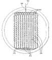
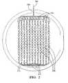
- FIG. 2is a perspective view of a wafer scale integration of antenna components, in an embodiment of the present invention
- FIG. 3is a schematic view of antenna elements having phase shifters as in FIG. 2 —that control the phase of radiation from the antenna elements, in which the present invention can be useful;
- FIG. 4is a diagrammatic sectional view of the wafer scale integration of antenna components as in FIG. 2 , in an embodiment of the present invention
- FIG. 5illustrates a schematic view of the wafer scale integration of antenna components as in FIG. 2 , in an embodiment of the present invention.
- FIG. 6is a graphical illustration of example applied control voltages to a barium strontanate titanate (BST) ferroelectric phase shifter and a measured capacitance response, in an embodiment of the present invention.
- BSTbarium strontanate titanate
- phase shiftersare fabricated en masse in a series of depositions along with other ESA components including phase shifter control lines and connections and radiating elements. En masse as used herein is defined as “as a whole.” Since the phase shifters are fabricated en masse along with other electronically scanned antenna components, a virtually unlimited number of phase shifters can be created for an antenna. Further, patterning of backside metal, vias and other expensive processes and steps are avoided utilizing the present invention.
- the phase shiftersinclude a ferroelectric material that is deposited on a low cost wafer scale substrate using a thin film process.
- Embodiments of the present inventionmay be utilized with radar and communication systems.
- Communications systems that can utilize the present inventioninclude point-to-point microwave links, links between buildings, and data links.
- Automotive safety sensorsincluding typical automotive radar frequencies of 24 GHz and 76 GHz
- military missile seeker systems using small aperture microwave and millimeter wave electronically scanned antennascan benefit from the present invention.
- FIG. 1Aillustrates a schematic view of a conventional two-dimensional scanning array 100 utilizing discrete integrated circuit phase shifters 102 .
- a microwave feed 104provides an input signal to the phase shifters 102 , and phase shifter control lines 108 provide DC signals to regulate the radiation phase of phase shifters 102 .
- the phase shifter control lines 108are directly connected to phase shifters 102 .
- Discrete integrated circuit phase shifters 102generate a radiation phase.
- Patch radiator 106radiates electromagnetic radio waves from an electromagnetic field about patch radiator 106 , generated by the radiation phase.
- fabrication expenseis increased due to the cost of the phase shifter components and the individual mounting of discrete phase shifters on a substrate or supporting structure.
- FIG. 1Bshows a diagrammatic sectional view of the supporting structure of the conventional two-dimensional scanning array as in FIG. 1A .
- the phase shifter integrated circuits 102are mounted to top metal for interconnects and patches 110 and a circuit board 114 .
- the ground plane metal 112provides a ground for the circuit.
- the phase shifter integrated circuits 102are individually assembled, packaged, individually positioned and mounted (soldered down) and individually tested on the antenna structure.
- FIG. 2is a perspective view of a wafer scale integration of antenna components, in an embodiment of the present invention.
- RF input 202feeds an RF signal to microstrip feed 208 .
- RF input 202can use a standard coaxial connection that interfaces with a quasi TEM of microstrip feed 208 with little loss.
- Microstrip feed 208passes on the RF signal to phase shifter 204 .
- the phase shifter 204a ferroelectric material, is a voltage variable dielectric, which generates a radiation phase.
- the radiation phase from phase shifter 204generates an electromagnetic field about the radiating elements 206 and electromagnetic radio waves are radiated from the radiating elements 206 .
- each phase shifter 204receives a predetermined voltage for regulating the phase shift and causing the antenna to scan.
- the radiation phase from each phase shifter 204 elementis regulated by a phase shifter control, which provides an analog DC control voltage or current. Analog control voltages are used when the phase shifter 204 must continuously change with voltage. With digital control voltages, the phase shifter 204 may jump by discrete bits.
- the pads for the DC phase shift 210are connected to the radiating elements 206 and supply the analog DC voltage for regulating the radiation phase. In an embodiment, DC control voltage pads 210 are connected using wirebonds to a circuit board interfacing with a ribbon cable. Additionally, termination resistors 212 , connected to the radiating elements 206 , suppress spurious lobes due to reflections from the end of the radiating elements 206 .
- FIG. 3a schematic view is shown of antenna elements 306 having phase shifters 304 that control the phase of radiation from the antenna elements 306 , as in FIG. 2 .
- Both one-dimensional and two-dimensional electronically scanned antennascan be fabricated at substantially the same cost.
- each line of radiating antenna elements 306requires one phase shifter 304 .
- 12 phase shiftersare employed.
- each radiating antenna element 306requires one phase shifter.
- an array of 144 phase shiftersis formed.
- each radiating antenna element 306 requiring one phase shifter 304can be fabricated for substantially the same cost as each line of radiating antenna elements 306 requiring one phase shifter 304 .
- the present inventionfabricates 144 phase shifters for substantially the same cost as 12 phase shifters.
- conventional systemsindividually assemble and mount phase shifters, and for each phase shifter mounted the cost increases.
- two-dimensional scanning requiring 144 phase shiftersis prohibitively costly for most applications.
- FIG. 4is a diagrammatic sectional view of the wafer scale integration of antenna components as in FIG. 2 .
- a wafer scale antennais provided in part to reduce the cost of small aperture arrays.
- Alternative wafer scale sizescan be utilized by the present invention to furnish a required antenna aperture area.
- a four-inch diameter waferis utilized.
- a larger wafer size and larger antennais employed for applications requiring a more directed beam and smaller beamwidth.
- a larger apertureis required and thus a larger wafer is employed.
- the first electrode 422i.e., platinum
- the ferroelectric layeris a barium strontanate titanate (BST) ferroelectric varactor.
- the first interconnect 410(for example, a gold Au interconnect metallization layer) acts as the radiating element.
- the first interconnect 410contacts the second interconnect 438 , and the second interconnect 438 acts as the radiating element.
- the microstrip feed, control lines and connections and radiating elementsare implemented on first interconnect 410 .
- the first interconnect 410contacts first electrode 422 .
- the passivation layer 430 and 436a non-conductive and inert material acts as a shield.
- the passivationis in part used to shield the phase shifters, since gold interconnects do not require passivation being nonreactive.
- the substrate 414is also inert and non-conductive.
- Antenna components of the present inventionare fabricated (grown) collectively including phase shifters, radiating elements, phase shifter control lines and connections and termination resistors. These components are fabricated en masse in a series of depositions including first interconnect 410 , first electrode 422 , ferroelectric layer 424 , second electrode 426 , and termination resistor layer (not shown). Passivation layers 430 , 436 and insulation 432 may further be deposited en masse. In contrast, conventionally, ferroelectric phase shifters are fabricated, individually divided, packaged and individually mounted on a further substrate. These components of the present invention are deposited on substrate 414 , which includes a ground plane metal layer 410 . A sapphire substrate may be used. Alternatively, a glass or quartz substrate may be used for lesser cost.
- Antenna elementsincluding radiators, ground plane, and resistive terminations are fabricated using standard foundry metallizations and depositions.
- the first electrode 422is selectively deposited partly across the wafer substrate.
- the ferroelectric layer 424is subsequently deposited.
- the second electrode 426is next deposited. Masking steps are used during deposition steps to properly position materials.
- first interconnect 410is deposited effecting the microstrip feed, control connections and radiating patches.
- An insulation 432 and second passivation layer 430may next be deposited along with the optional second interconnect 438 . In an example, a 4-inch, 500 ⁇ m thick substrate is utilized.
- variable capacitoris deposited on a low cost insulating wafer scale substrate with high-quality passives using a thin film process.
- Thin film processesthat can be employed include sputtering, and chemical vapor deposition (CVD) such as metal-organic chemical vapor deposition (MOCVD).
- CVDchemical vapor deposition
- MOCVDmetal-organic chemical vapor deposition
- the phase shiftersmay be deposited en masse along with other antenna components, rather than being individually mounted on an antenna.
- Thin film processesare employed for advantages as discussed in FIG. 6 , infra.
- the radiating elements and external connectionsmake up a single metallization layer.
- the phase shiftersare symmetrical and balanced and provide a transition from an unbalanced to a balanced structure. That is, the microstrip feed includes a ground connection (sapphire substrate) and a connection out to the radiating elements and the phase shifter control. This is an asymmetrical and unbalanced structure.
- the phase shiftersare fabricated with two parallel lines and a BST deposit. In an embodiment, the phase shifters provide a shunt from the input to the phase shifter control connections.
- FIG. 5illustrates a schematic view of the wafer scale integration of antenna components as in FIG. 2 .
- individual phase shifter control lines 510are utilized to connect a DC phase shifter control to a phase shifter 504 .
- the antenna array itself(the radiating elements 506 ) are utilized as a DC phase shifter control distribution network, and thus separate phase shifter control lines are not required.
- the phase shifter controlsare physically connected to the variable capacitor via the radiating elements.
- FIG. 6shows a graphical illustration of example applied control voltages to a BST ferroelectric phase shifter and a measured capacitance response.
- thin-film ferroelectricsrequire only a moderate voltage change to adjust the capacitance.
- the useable tunability of the thin-film BSTis 2:1 or more. That is, changing the capacitance of the ferroelectric material with an applied voltage gives the ferroelectric material the ability to tune the capacitance over a wide range of at least a 2:1 capacitance to voltage change.
- Ferroelectric materialsexhibit a high capacitance density and so a large value capacitor can be constructed in a small physical area. Since small tunable capacitors can be formed, many can be constructed on a single wafer.
- the present inventionprovides a voltage variable dielectric having a high capacitance density (10 to 20 nF/mm 2 ), and a wide range of control voltages is utilized, i.e., 5 to 30 volts. In an example, diode-conduction is not observed, the BST operating at zero bias with large AC swings.
Landscapes
- Engineering & Computer Science (AREA)
- Manufacturing & Machinery (AREA)
- Variable-Direction Aerials And Aerial Arrays (AREA)
- Waveguide Switches, Polarizers, And Phase Shifters (AREA)
Abstract
Description
Claims (20)
Priority Applications (2)
| Application Number | Priority Date | Filing Date | Title |
|---|---|---|---|
| US11/219,400US7324043B2 (en) | 2005-09-02 | 2005-09-02 | Phase shifters deposited en masse for an electronically scanned antenna |
| EP06076621.9AEP1760829B1 (en) | 2005-09-02 | 2006-08-25 | Phase shifters deposited en masse for an electronically scanned antenna |
Applications Claiming Priority (1)
| Application Number | Priority Date | Filing Date | Title |
|---|---|---|---|
| US11/219,400US7324043B2 (en) | 2005-09-02 | 2005-09-02 | Phase shifters deposited en masse for an electronically scanned antenna |
Publications (2)
| Publication Number | Publication Date |
|---|---|
| US20070052592A1 US20070052592A1 (en) | 2007-03-08 |
| US7324043B2true US7324043B2 (en) | 2008-01-29 |
Family
ID=37491731
Family Applications (1)
| Application Number | Title | Priority Date | Filing Date |
|---|---|---|---|
| US11/219,400Active2026-05-03US7324043B2 (en) | 2005-09-02 | 2005-09-02 | Phase shifters deposited en masse for an electronically scanned antenna |
Country Status (2)
| Country | Link |
|---|---|
| US (1) | US7324043B2 (en) |
| EP (1) | EP1760829B1 (en) |
Cited By (34)
| Publication number | Priority date | Publication date | Assignee | Title |
|---|---|---|---|---|
| US20090270059A1 (en)* | 2008-04-28 | 2009-10-29 | Bally Nazar F | Receiver system and method for receiving signals |
| US20100201816A1 (en)* | 2009-02-06 | 2010-08-12 | Lee Ethan J | Multi-display mirror system and method for expanded view around a vehicle |
| US7918570B2 (en) | 2002-06-06 | 2011-04-05 | Donnelly Corporation | Vehicular interior rearview information mirror system |
| US7994471B2 (en) | 1998-01-07 | 2011-08-09 | Donnelly Corporation | Interior rearview mirror system with forwardly-viewing camera |
| US8000894B2 (en) | 2000-03-02 | 2011-08-16 | Donnelly Corporation | Vehicular wireless communication system |
| US8019505B2 (en) | 2003-10-14 | 2011-09-13 | Donnelly Corporation | Vehicle information display |
| US8063753B2 (en) | 1997-08-25 | 2011-11-22 | Donnelly Corporation | Interior rearview mirror system |
| US8094002B2 (en) | 1998-01-07 | 2012-01-10 | Donnelly Corporation | Interior rearview mirror system |
| US8100568B2 (en) | 1997-08-25 | 2012-01-24 | Donnelly Corporation | Interior rearview mirror system for a vehicle |
| US8106347B2 (en) | 2002-05-03 | 2012-01-31 | Donnelly Corporation | Vehicle rearview mirror system |
| US8164817B2 (en) | 1994-05-05 | 2012-04-24 | Donnelly Corporation | Method of forming a mirrored bent cut glass shape for vehicular exterior rearview mirror assembly |
| US8162493B2 (en) | 1999-11-24 | 2012-04-24 | Donnelly Corporation | Interior rearview mirror assembly for vehicle |
| US8179586B2 (en) | 2003-10-02 | 2012-05-15 | Donnelly Corporation | Rearview mirror assembly for vehicle |
| US8228588B2 (en) | 2002-09-20 | 2012-07-24 | Donnelly Corporation | Interior rearview mirror information display system for a vehicle |
| US8237909B2 (en) | 2009-02-06 | 2012-08-07 | Gentex Corporation | Vehicular rearview mirror assembly including integrated backlighting for a liquid crystal display (LCD) |
| US8282253B2 (en) | 2004-11-22 | 2012-10-09 | Donnelly Corporation | Mirror reflective element sub-assembly for exterior rearview mirror of a vehicle |
| US8288711B2 (en) | 1998-01-07 | 2012-10-16 | Donnelly Corporation | Interior rearview mirror system with forwardly-viewing camera and a control |
| US8335032B2 (en) | 2002-09-20 | 2012-12-18 | Donnelly Corporation | Reflective mirror assembly |
| US8427288B2 (en) | 2000-03-02 | 2013-04-23 | Donnelly Corporation | Rear vision system for a vehicle |
| US20130141295A1 (en)* | 2011-06-06 | 2013-06-06 | University Of Dayton | Miniaturized and reconfigurable cpw square-ring slot antenna including ferroelectric bst varactors |
| US8465163B2 (en) | 2002-06-06 | 2013-06-18 | Donnelly Corporation | Interior rearview mirror system |
| US20130188041A1 (en)* | 2012-01-19 | 2013-07-25 | Canon Kabushiki Kaisha | Detecting device, detector, and imaging apparatus using the same |
| US8503062B2 (en) | 2005-05-16 | 2013-08-06 | Donnelly Corporation | Rearview mirror element assembly for vehicle |
| US8508383B2 (en) | 2008-03-31 | 2013-08-13 | Magna Mirrors of America, Inc | Interior rearview mirror system |
| US8511841B2 (en) | 1994-05-05 | 2013-08-20 | Donnelly Corporation | Vehicular blind spot indicator mirror |
| US8525703B2 (en) | 1998-04-08 | 2013-09-03 | Donnelly Corporation | Interior rearview mirror system |
| US8610992B2 (en) | 1997-08-25 | 2013-12-17 | Donnelly Corporation | Variable transmission window |
| US8653959B2 (en) | 2001-01-23 | 2014-02-18 | Donnelly Corporation | Video mirror system for a vehicle |
| US8908039B2 (en) | 2000-03-02 | 2014-12-09 | Donnelly Corporation | Vehicular video mirror system |
| US9019091B2 (en) | 1999-11-24 | 2015-04-28 | Donnelly Corporation | Interior rearview mirror system |
| US9041806B2 (en) | 2009-09-01 | 2015-05-26 | Magna Electronics Inc. | Imaging and display system for vehicle |
| US9264672B2 (en) | 2010-12-22 | 2016-02-16 | Magna Mirrors Of America, Inc. | Vision display system for vehicle |
| US9809171B2 (en) | 2000-03-02 | 2017-11-07 | Magna Electronics Inc. | Vision system for vehicle |
| US11994272B2 (en) | 2021-08-20 | 2024-05-28 | Gentex Corporation | Lighting assembly and illumination system having a lighting assembly |
Families Citing this family (12)
| Publication number | Priority date | Publication date | Assignee | Title |
|---|---|---|---|---|
| US7324043B2 (en)* | 2005-09-02 | 2008-01-29 | Delphi Technologies, Inc. | Phase shifters deposited en masse for an electronically scanned antenna |
| DE102011089639A1 (en)* | 2011-12-22 | 2013-06-27 | Siemens Aktiengesellschaft | Circuit carrier with a separate RF circuit and method for assembling such a circuit carrier |
| US9178276B1 (en)* | 2013-02-15 | 2015-11-03 | Rockwell Collins, Inc. | Widely varied reconfigurable aperture antenna system utilizing ultra-fast transitioned aperture material |
| CN104638352A (en)* | 2013-11-13 | 2015-05-20 | 深圳光启创新技术有限公司 | Ultra-broadband patch antenna |
| WO2017121477A1 (en)* | 2016-01-14 | 2017-07-20 | Huawei Technologies Co., Ltd. | Phased antenna array device |
| CN108879108B (en)* | 2018-07-06 | 2020-09-29 | 电子科技大学 | Reconfigurable phased array antenna RCS reduction method based on scattering polarization |
| US11340329B2 (en)* | 2018-12-07 | 2022-05-24 | Apple Inc. | Electronic devices with broadband ranging capabilities |
| US11664593B1 (en) | 2020-05-18 | 2023-05-30 | Amazon Technologies, Inc. | Antenna module with feed elements on a triangular lattice for antenna arrays |
| US11641067B1 (en)* | 2020-05-18 | 2023-05-02 | Amazon Technologies, Inc. | Passive antenna elements used to fill gaps in a paneltzed phased array antenna |
| US12323180B2 (en) | 2021-04-21 | 2025-06-03 | Skyworks Solutions, Inc. | Antenna array with antenna elements interconnected by controllable resistances |
| US11916303B2 (en)* | 2021-04-21 | 2024-02-27 | Skyworks Solutions, Inc. | Antenna array having antenna elements interconnected by material for controlling beamforming |
| EP4352819A4 (en)* | 2021-06-08 | 2025-04-30 | SPRA Savunma Havacilik ve Uzay Teknolojileri Elektronik Yazilim Makina Sanyi ve Ticaret Limited Sirketi | COMPACT BEAMFORMING MODULE FOR PHASE-STACKED ARRANGE ANTENNA SYSTEMS |
Citations (17)
| Publication number | Priority date | Publication date | Assignee | Title |
|---|---|---|---|---|
| US3454945A (en)* | 1964-09-18 | 1969-07-08 | Texas Instruments Inc | Modular integrated electronics radar |
| US3750055A (en)* | 1969-12-16 | 1973-07-31 | Thomas Csf | Integrated phase-shifting microcircuit |
| US4382261A (en)* | 1980-05-05 | 1983-05-03 | The United States Of America As Represented By The Secretary Of The Army | Phase shifter and line scanner for phased array applications |
| FR2538188A1 (en)* | 1982-12-16 | 1984-06-22 | Dreuilhe Jacqueline | Oscillator for Doppler effect radar head for detecting moving objects. |
| US4675628A (en)* | 1985-02-28 | 1987-06-23 | Rca Corporation | Distributed pin diode phase shifter |
| US5329255A (en)* | 1992-09-04 | 1994-07-12 | Trw Inc. | Thermally compensating microwave cavity |
| US5617103A (en) | 1995-07-19 | 1997-04-01 | The United States Of America As Represented By The Secretary Of The Army | Ferroelectric phase shifting antenna array |
| US5680073A (en)* | 1993-06-08 | 1997-10-21 | Ramot University Authority For Applied Research & Industrial Development Ltd. | Controlled semiconductor capacitors |
| US5721194A (en) | 1992-12-01 | 1998-02-24 | Superconducting Core Technologies, Inc. | Tuneable microwave devices including fringe effect capacitor incorporating ferroelectric films |
| US20020175878A1 (en) | 2001-04-11 | 2002-11-28 | Toncich Stanley S. | Tunable matching circuit |
| US20040063566A1 (en)* | 2002-09-27 | 2004-04-01 | Christopher Caspers | Dielectric composite materials including an electronically tunable dielectric phase and a calcium and oxygen-containing compound phase |
| US20040089985A1 (en)* | 2001-01-24 | 2004-05-13 | Sengupta Louise C. | Electronically tunable, low-loss ceramic materials including a tunable dielectric phase and multiple metal oxide phases |
| GB2406443A (en) | 2003-09-25 | 2005-03-30 | Bosch Gmbh Robert | Phase Shifter Having An Adjustable Thin Film Capacitor |
| US6999040B2 (en)* | 2003-06-18 | 2006-02-14 | Raytheon Company | Transverse device array phase shifter circuit techniques and antennas |
| US20060060900A1 (en)* | 2004-09-20 | 2006-03-23 | Xubai Zhang | Tunable low loss material composition and methods of manufacture and use therefore |
| US7173503B1 (en)* | 2004-07-29 | 2007-02-06 | Lockheed Martin Corporation | Multibit phase shifter with active and passive phase bits, and active phase bit therefor |
| US20070052592A1 (en)* | 2005-09-02 | 2007-03-08 | Purden George J | Phase shifters deposited en masse for an electronically scanned antenna |
- 2005
- 2005-09-02USUS11/219,400patent/US7324043B2/enactiveActive
- 2006
- 2006-08-25EPEP06076621.9Apatent/EP1760829B1/enactiveActive
Patent Citations (17)
| Publication number | Priority date | Publication date | Assignee | Title |
|---|---|---|---|---|
| US3454945A (en)* | 1964-09-18 | 1969-07-08 | Texas Instruments Inc | Modular integrated electronics radar |
| US3750055A (en)* | 1969-12-16 | 1973-07-31 | Thomas Csf | Integrated phase-shifting microcircuit |
| US4382261A (en)* | 1980-05-05 | 1983-05-03 | The United States Of America As Represented By The Secretary Of The Army | Phase shifter and line scanner for phased array applications |
| FR2538188A1 (en)* | 1982-12-16 | 1984-06-22 | Dreuilhe Jacqueline | Oscillator for Doppler effect radar head for detecting moving objects. |
| US4675628A (en)* | 1985-02-28 | 1987-06-23 | Rca Corporation | Distributed pin diode phase shifter |
| US5329255A (en)* | 1992-09-04 | 1994-07-12 | Trw Inc. | Thermally compensating microwave cavity |
| US5721194A (en) | 1992-12-01 | 1998-02-24 | Superconducting Core Technologies, Inc. | Tuneable microwave devices including fringe effect capacitor incorporating ferroelectric films |
| US5680073A (en)* | 1993-06-08 | 1997-10-21 | Ramot University Authority For Applied Research & Industrial Development Ltd. | Controlled semiconductor capacitors |
| US5617103A (en) | 1995-07-19 | 1997-04-01 | The United States Of America As Represented By The Secretary Of The Army | Ferroelectric phase shifting antenna array |
| US20040089985A1 (en)* | 2001-01-24 | 2004-05-13 | Sengupta Louise C. | Electronically tunable, low-loss ceramic materials including a tunable dielectric phase and multiple metal oxide phases |
| US20020175878A1 (en) | 2001-04-11 | 2002-11-28 | Toncich Stanley S. | Tunable matching circuit |
| US20040063566A1 (en)* | 2002-09-27 | 2004-04-01 | Christopher Caspers | Dielectric composite materials including an electronically tunable dielectric phase and a calcium and oxygen-containing compound phase |
| US6999040B2 (en)* | 2003-06-18 | 2006-02-14 | Raytheon Company | Transverse device array phase shifter circuit techniques and antennas |
| GB2406443A (en) | 2003-09-25 | 2005-03-30 | Bosch Gmbh Robert | Phase Shifter Having An Adjustable Thin Film Capacitor |
| US7173503B1 (en)* | 2004-07-29 | 2007-02-06 | Lockheed Martin Corporation | Multibit phase shifter with active and passive phase bits, and active phase bit therefor |
| US20060060900A1 (en)* | 2004-09-20 | 2006-03-23 | Xubai Zhang | Tunable low loss material composition and methods of manufacture and use therefore |
| US20070052592A1 (en)* | 2005-09-02 | 2007-03-08 | Purden George J | Phase shifters deposited en masse for an electronically scanned antenna |
Non-Patent Citations (3)
| Title |
|---|
| Database Inspec [Online] The Institute of Electrical Engineers, Stevenage, GB; 2001, York R et al: "Microwave integrated circuits using thin-film BST" XP002411793 Database Accession No. 7137789 *abstract* & ISAF 2000. Proceedings of the 2000 12<SUP>th </SUP>IEEE. |
| EP Search Report dated Jan. 31, 2007. |
| International Symposium on Application of Ferroelectrics Jul. 21-Aug. 2, 2000 Honolulu, HI, USA, vol. 1, Jul. 21, 2000,-Aug. 2, 2000 pp. 195-200 vol. ISAF 2000. Proceedings of the 2000 12<SUP>th </SUP>IEEE International Symposium on Applications of Ferroelectrics (IEEE Cat. No. 00CH37076) IEEE Piscataway, NJ, USA ISBN: 0-7803-5940-2. |
Cited By (115)
| Publication number | Priority date | Publication date | Assignee | Title |
|---|---|---|---|---|
| US8164817B2 (en) | 1994-05-05 | 2012-04-24 | Donnelly Corporation | Method of forming a mirrored bent cut glass shape for vehicular exterior rearview mirror assembly |
| US8511841B2 (en) | 1994-05-05 | 2013-08-20 | Donnelly Corporation | Vehicular blind spot indicator mirror |
| US8559093B2 (en) | 1995-04-27 | 2013-10-15 | Donnelly Corporation | Electrochromic mirror reflective element for vehicular rearview mirror assembly |
| US8100568B2 (en) | 1997-08-25 | 2012-01-24 | Donnelly Corporation | Interior rearview mirror system for a vehicle |
| US8267559B2 (en) | 1997-08-25 | 2012-09-18 | Donnelly Corporation | Interior rearview mirror assembly for a vehicle |
| US8610992B2 (en) | 1997-08-25 | 2013-12-17 | Donnelly Corporation | Variable transmission window |
| US8779910B2 (en) | 1997-08-25 | 2014-07-15 | Donnelly Corporation | Interior rearview mirror system |
| US8063753B2 (en) | 1997-08-25 | 2011-11-22 | Donnelly Corporation | Interior rearview mirror system |
| US8325028B2 (en) | 1998-01-07 | 2012-12-04 | Donnelly Corporation | Interior rearview mirror system |
| US8094002B2 (en) | 1998-01-07 | 2012-01-10 | Donnelly Corporation | Interior rearview mirror system |
| US8288711B2 (en) | 1998-01-07 | 2012-10-16 | Donnelly Corporation | Interior rearview mirror system with forwardly-viewing camera and a control |
| US8134117B2 (en) | 1998-01-07 | 2012-03-13 | Donnelly Corporation | Vehicular having a camera, a rain sensor and a single-ball interior electrochromic mirror assembly attached at an attachment element |
| US7994471B2 (en) | 1998-01-07 | 2011-08-09 | Donnelly Corporation | Interior rearview mirror system with forwardly-viewing camera |
| US9481306B2 (en) | 1998-04-08 | 2016-11-01 | Donnelly Corporation | Automotive communication system |
| US8884788B2 (en) | 1998-04-08 | 2014-11-11 | Donnelly Corporation | Automotive communication system |
| US9221399B2 (en) | 1998-04-08 | 2015-12-29 | Magna Mirrors Of America, Inc. | Automotive communication system |
| US8525703B2 (en) | 1998-04-08 | 2013-09-03 | Donnelly Corporation | Interior rearview mirror system |
| US9019091B2 (en) | 1999-11-24 | 2015-04-28 | Donnelly Corporation | Interior rearview mirror system |
| US8162493B2 (en) | 1999-11-24 | 2012-04-24 | Donnelly Corporation | Interior rearview mirror assembly for vehicle |
| US10144355B2 (en) | 1999-11-24 | 2018-12-04 | Donnelly Corporation | Interior rearview mirror system for vehicle |
| US9376061B2 (en) | 1999-11-24 | 2016-06-28 | Donnelly Corporation | Accessory system of a vehicle |
| US9278654B2 (en) | 1999-11-24 | 2016-03-08 | Donnelly Corporation | Interior rearview mirror system for vehicle |
| US10053013B2 (en) | 2000-03-02 | 2018-08-21 | Magna Electronics Inc. | Vision system for vehicle |
| US8427288B2 (en) | 2000-03-02 | 2013-04-23 | Donnelly Corporation | Rear vision system for a vehicle |
| US8543330B2 (en) | 2000-03-02 | 2013-09-24 | Donnelly Corporation | Driver assist system for vehicle |
| US8000894B2 (en) | 2000-03-02 | 2011-08-16 | Donnelly Corporation | Vehicular wireless communication system |
| US8676491B2 (en) | 2000-03-02 | 2014-03-18 | Magna Electronics Inc. | Driver assist system for vehicle |
| US10179545B2 (en) | 2000-03-02 | 2019-01-15 | Magna Electronics Inc. | Park-aid system for vehicle |
| US9315151B2 (en) | 2000-03-02 | 2016-04-19 | Magna Electronics Inc. | Driver assist system for vehicle |
| US9783114B2 (en) | 2000-03-02 | 2017-10-10 | Donnelly Corporation | Vehicular video mirror system |
| US9809171B2 (en) | 2000-03-02 | 2017-11-07 | Magna Electronics Inc. | Vision system for vehicle |
| US9809168B2 (en) | 2000-03-02 | 2017-11-07 | Magna Electronics Inc. | Driver assist system for vehicle |
| US9014966B2 (en) | 2000-03-02 | 2015-04-21 | Magna Electronics Inc. | Driver assist system for vehicle |
| US8121787B2 (en) | 2000-03-02 | 2012-02-21 | Donnelly Corporation | Vehicular video mirror system |
| US8271187B2 (en) | 2000-03-02 | 2012-09-18 | Donnelly Corporation | Vehicular video mirror system |
| US8908039B2 (en) | 2000-03-02 | 2014-12-09 | Donnelly Corporation | Vehicular video mirror system |
| US10239457B2 (en) | 2000-03-02 | 2019-03-26 | Magna Electronics Inc. | Vehicular vision system |
| US10131280B2 (en) | 2000-03-02 | 2018-11-20 | Donnelly Corporation | Vehicular video mirror system |
| US10272839B2 (en) | 2001-01-23 | 2019-04-30 | Magna Electronics Inc. | Rear seat occupant monitoring system for vehicle |
| US9352623B2 (en) | 2001-01-23 | 2016-05-31 | Magna Electronics Inc. | Trailer hitching aid system for vehicle |
| US9694749B2 (en) | 2001-01-23 | 2017-07-04 | Magna Electronics Inc. | Trailer hitching aid system for vehicle |
| US8653959B2 (en) | 2001-01-23 | 2014-02-18 | Donnelly Corporation | Video mirror system for a vehicle |
| US8654433B2 (en) | 2001-01-23 | 2014-02-18 | Magna Mirrors Of America, Inc. | Rearview mirror assembly for vehicle |
| US8106347B2 (en) | 2002-05-03 | 2012-01-31 | Donnelly Corporation | Vehicle rearview mirror system |
| US8304711B2 (en) | 2002-05-03 | 2012-11-06 | Donnelly Corporation | Vehicle rearview mirror system |
| US8608327B2 (en) | 2002-06-06 | 2013-12-17 | Donnelly Corporation | Automatic compass system for vehicle |
| US7918570B2 (en) | 2002-06-06 | 2011-04-05 | Donnelly Corporation | Vehicular interior rearview information mirror system |
| US8047667B2 (en) | 2002-06-06 | 2011-11-01 | Donnelly Corporation | Vehicular interior rearview mirror system |
| US8465162B2 (en) | 2002-06-06 | 2013-06-18 | Donnelly Corporation | Vehicular interior rearview mirror system |
| US8177376B2 (en) | 2002-06-06 | 2012-05-15 | Donnelly Corporation | Vehicular interior rearview mirror system |
| US8465163B2 (en) | 2002-06-06 | 2013-06-18 | Donnelly Corporation | Interior rearview mirror system |
| US8797627B2 (en) | 2002-09-20 | 2014-08-05 | Donnelly Corporation | Exterior rearview mirror assembly |
| US8228588B2 (en) | 2002-09-20 | 2012-07-24 | Donnelly Corporation | Interior rearview mirror information display system for a vehicle |
| US10661716B2 (en) | 2002-09-20 | 2020-05-26 | Donnelly Corporation | Vehicular exterior electrically variable reflectance mirror reflective element assembly |
| US10029616B2 (en) | 2002-09-20 | 2018-07-24 | Donnelly Corporation | Rearview mirror assembly for vehicle |
| US10363875B2 (en) | 2002-09-20 | 2019-07-30 | Donnelly Corportion | Vehicular exterior electrically variable reflectance mirror reflective element assembly |
| US8335032B2 (en) | 2002-09-20 | 2012-12-18 | Donnelly Corporation | Reflective mirror assembly |
| US8400704B2 (en) | 2002-09-20 | 2013-03-19 | Donnelly Corporation | Interior rearview mirror system for a vehicle |
| US9073491B2 (en) | 2002-09-20 | 2015-07-07 | Donnelly Corporation | Exterior rearview mirror assembly |
| US9545883B2 (en) | 2002-09-20 | 2017-01-17 | Donnelly Corporation | Exterior rearview mirror assembly |
| US8179586B2 (en) | 2003-10-02 | 2012-05-15 | Donnelly Corporation | Rearview mirror assembly for vehicle |
| US8705161B2 (en) | 2003-10-02 | 2014-04-22 | Donnelly Corporation | Method of manufacturing a reflective element for a vehicular rearview mirror assembly |
| US8379289B2 (en) | 2003-10-02 | 2013-02-19 | Donnelly Corporation | Rearview mirror assembly for vehicle |
| US8095260B1 (en) | 2003-10-14 | 2012-01-10 | Donnelly Corporation | Vehicle information display |
| US8019505B2 (en) | 2003-10-14 | 2011-09-13 | Donnelly Corporation | Vehicle information display |
| US8355839B2 (en) | 2003-10-14 | 2013-01-15 | Donnelly Corporation | Vehicle vision system with night vision function |
| US8170748B1 (en) | 2003-10-14 | 2012-05-01 | Donnelly Corporation | Vehicle information display system |
| US8577549B2 (en) | 2003-10-14 | 2013-11-05 | Donnelly Corporation | Information display system for a vehicle |
| US8282253B2 (en) | 2004-11-22 | 2012-10-09 | Donnelly Corporation | Mirror reflective element sub-assembly for exterior rearview mirror of a vehicle |
| US8503062B2 (en) | 2005-05-16 | 2013-08-06 | Donnelly Corporation | Rearview mirror element assembly for vehicle |
| US10308186B2 (en) | 2005-09-14 | 2019-06-04 | Magna Mirrors Of America, Inc. | Vehicular exterior rearview mirror assembly with blind spot indicator |
| US8833987B2 (en) | 2005-09-14 | 2014-09-16 | Donnelly Corporation | Mirror reflective element sub-assembly for exterior rearview mirror of a vehicle |
| US10829053B2 (en) | 2005-09-14 | 2020-11-10 | Magna Mirrors Of America, Inc. | Vehicular exterior rearview mirror assembly with blind spot indicator |
| US9694753B2 (en) | 2005-09-14 | 2017-07-04 | Magna Mirrors Of America, Inc. | Mirror reflective element sub-assembly for exterior rearview mirror of a vehicle |
| US11072288B2 (en) | 2005-09-14 | 2021-07-27 | Magna Mirrors Of America, Inc. | Vehicular exterior rearview mirror assembly with blind spot indicator element |
| US9758102B1 (en) | 2005-09-14 | 2017-09-12 | Magna Mirrors Of America, Inc. | Mirror reflective element sub-assembly for exterior rearview mirror of a vehicle |
| US9045091B2 (en) | 2005-09-14 | 2015-06-02 | Donnelly Corporation | Mirror reflective element sub-assembly for exterior rearview mirror of a vehicle |
| US10150417B2 (en) | 2005-09-14 | 2018-12-11 | Magna Mirrors Of America, Inc. | Mirror reflective element sub-assembly for exterior rearview mirror of a vehicle |
| US11285879B2 (en) | 2005-09-14 | 2022-03-29 | Magna Mirrors Of America, Inc. | Vehicular exterior rearview mirror assembly with blind spot indicator element |
| US11970113B2 (en) | 2005-11-01 | 2024-04-30 | Magna Electronics Inc. | Vehicular vision system |
| US11124121B2 (en) | 2005-11-01 | 2021-09-21 | Magna Electronics Inc. | Vehicular vision system |
| US8508383B2 (en) | 2008-03-31 | 2013-08-13 | Magna Mirrors of America, Inc | Interior rearview mirror system |
| US10175477B2 (en) | 2008-03-31 | 2019-01-08 | Magna Mirrors Of America, Inc. | Display system for vehicle |
| US8107915B2 (en) | 2008-04-28 | 2012-01-31 | Delphi Technologies, Inc. | Receiver system and method for receiving signals |
| US20090270059A1 (en)* | 2008-04-28 | 2009-10-29 | Bally Nazar F | Receiver system and method for receiving signals |
| US20100201816A1 (en)* | 2009-02-06 | 2010-08-12 | Lee Ethan J | Multi-display mirror system and method for expanded view around a vehicle |
| US8237909B2 (en) | 2009-02-06 | 2012-08-07 | Gentex Corporation | Vehicular rearview mirror assembly including integrated backlighting for a liquid crystal display (LCD) |
| US8411245B2 (en) | 2009-02-06 | 2013-04-02 | Gentex Corporation | Multi-display mirror system and method for expanded view around a vehicle |
| US10053012B2 (en) | 2009-09-01 | 2018-08-21 | Magna Electronics Inc. | Imaging and display system for vehicle |
| US9041806B2 (en) | 2009-09-01 | 2015-05-26 | Magna Electronics Inc. | Imaging and display system for vehicle |
| US9789821B2 (en) | 2009-09-01 | 2017-10-17 | Magna Electronics Inc. | Imaging and display system for vehicle |
| US11285877B2 (en) | 2009-09-01 | 2022-03-29 | Magna Electronics Inc. | Vehicular vision system |
| US11794651B2 (en) | 2009-09-01 | 2023-10-24 | Magna Electronics Inc. | Vehicular vision system |
| US10300856B2 (en) | 2009-09-01 | 2019-05-28 | Magna Electronics Inc. | Vehicular display system |
| US10875455B2 (en) | 2009-09-01 | 2020-12-29 | Magna Electronics Inc. | Vehicular vision system |
| US12296750B2 (en) | 2009-09-01 | 2025-05-13 | Magna Electronics Inc. | Vehicular vision system |
| US11155211B2 (en) | 2010-12-22 | 2021-10-26 | Magna Electronics Inc. | Vehicular multi-camera surround view system with video display |
| US9731653B2 (en) | 2010-12-22 | 2017-08-15 | Magna Electronics Inc. | Vision display system for vehicle |
| US10486597B1 (en) | 2010-12-22 | 2019-11-26 | Magna Electronics Inc. | Vehicular vision system with rear backup video display |
| US10814785B2 (en) | 2010-12-22 | 2020-10-27 | Magna Electronics Inc. | Vehicular rear backup vision system with video display |
| US10336255B2 (en) | 2010-12-22 | 2019-07-02 | Magna Electronics Inc. | Vehicular vision system with rear backup video display |
| US10589678B1 (en) | 2010-12-22 | 2020-03-17 | Magna Electronics Inc. | Vehicular rear backup vision system with video display |
| US9598014B2 (en) | 2010-12-22 | 2017-03-21 | Magna Electronics Inc. | Vision display system for vehicle |
| US10144352B2 (en) | 2010-12-22 | 2018-12-04 | Magna Electronics Inc. | Vision display system for vehicle |
| US9469250B2 (en) | 2010-12-22 | 2016-10-18 | Magna Electronics Inc. | Vision display system for vehicle |
| US12017588B2 (en) | 2010-12-22 | 2024-06-25 | Magna Electronics Inc. | Vehicular rear backup system with video display |
| US9264672B2 (en) | 2010-12-22 | 2016-02-16 | Magna Mirrors Of America, Inc. | Vision display system for vehicle |
| US11548444B2 (en) | 2010-12-22 | 2023-01-10 | Magna Electronics Inc. | Vehicular multi-camera surround view system with video display |
| US11708026B2 (en) | 2010-12-22 | 2023-07-25 | Magna Electronics Inc. | Vehicular rear backup system with video display |
| US20130141295A1 (en)* | 2011-06-06 | 2013-06-06 | University Of Dayton | Miniaturized and reconfigurable cpw square-ring slot antenna including ferroelectric bst varactors |
| US8957817B2 (en)* | 2011-06-06 | 2015-02-17 | University Of Dayton | Miniaturized and reconfigurable CPW square-ring slot antenna including ferroelectric BST varactors |
| US9437646B2 (en)* | 2012-01-19 | 2016-09-06 | Canon Kabushiki Kaisha | Detecting device, detector, and imaging apparatus using the same |
| US20130188041A1 (en)* | 2012-01-19 | 2013-07-25 | Canon Kabushiki Kaisha | Detecting device, detector, and imaging apparatus using the same |
| US11994272B2 (en) | 2021-08-20 | 2024-05-28 | Gentex Corporation | Lighting assembly and illumination system having a lighting assembly |
| US12435864B2 (en) | 2021-08-20 | 2025-10-07 | Gentex Corporation | Lighting assembly and illumination system having a lighting assembly |
Also Published As
| Publication number | Publication date |
|---|---|
| EP1760829A1 (en) | 2007-03-07 |
| EP1760829B1 (en) | 2014-04-16 |
| US20070052592A1 (en) | 2007-03-08 |
Similar Documents
| Publication | Publication Date | Title |
|---|---|---|
| US7324043B2 (en) | Phase shifters deposited en masse for an electronically scanned antenna | |
| US6335703B1 (en) | Patch antenna with finite ground plane | |
| US6806846B1 (en) | Frequency agile material-based reflectarray antenna | |
| EP1502323B1 (en) | Reflect array antenna with assymetrically switched antenna elements | |
| CN101743665B (en) | Improvements in Reconfigurable Antennas and Improvements Related thereto | |
| US10355356B2 (en) | Metamaterial-based phase shifting element and phased array | |
| EP3401999A1 (en) | Luneberg lens antenna device | |
| CN109891673A (en) | The reconfigurable super surface reflector antenna of liquid crystal | |
| WO2004091040A2 (en) | Cavity embedded antenna | |
| JP2024510409A (en) | Metasurface antenna with integrated varactor circuit | |
| Trampler et al. | Phase-agile dual-resonance single linearly polarized antenna element for reconfigurable reflectarray applications | |
| US12062864B2 (en) | High gain and fan beam antenna structures | |
| US20030184477A1 (en) | Phased array antenna steering arrangements | |
| US12062863B2 (en) | Antenna device | |
| US6894655B1 (en) | Phased array antenna with selective capacitive coupling and associated methods | |
| Zhai et al. | mm-Wave large-scale phased array based on randomly tiled rectangular sub-arrays for 5G communications | |
| US20050099354A1 (en) | Multiband radially distributed phased array antenna with a sloping ground plane and associated methods | |
| NL2023908B1 (en) | Antenna device which is suitable for wireless communications according to a 5g network standard, rf transceiver containing an antenna device, and method for use in wireless communications according to a 5g network standard. | |
| US6954179B2 (en) | Multiband radially distributed graded phased array antenna and associated methods | |
| EP4250486A1 (en) | Radial line slot antenna arrays | |
| US12155105B2 (en) | TSV phase shifter | |
| GB2616848A (en) | Radial line slot antenna arrays | |
| Gautier et al. | Hybrid integrated RF-MEMS phased array antenna at 10GHz | |
| Shi et al. | A 24 GHz wafer scale electronically scanned antenna using BST phase shifters for collision avoidance systems | |
| Shi et al. | Wideband circularly polarized ltcc modular phased array antenna at ka-band |
Legal Events
| Date | Code | Title | Description |
|---|---|---|---|
| AS | Assignment | Owner name:DELPHI TECHNOLOGIES, INC., MICHIGAN Free format text:ASSIGNMENT OF ASSIGNORS INTEREST;ASSIGNORS:PURDEN, GEORGE J.;SHI, SHAWN;REEL/FRAME:016961/0883 Effective date:20050829 | |
| STCF | Information on status: patent grant | Free format text:PATENTED CASE | |
| FPAY | Fee payment | Year of fee payment:4 | |
| FPAY | Fee payment | Year of fee payment:8 | |
| AS | Assignment | Owner name:APTIV TECHNOLOGIES LIMITED, BARBADOS Free format text:ASSIGNMENT OF ASSIGNORS INTEREST;ASSIGNOR:DELPHI TECHNOLOGIES INC.;REEL/FRAME:047143/0874 Effective date:20180101 | |
| MAFP | Maintenance fee payment | Free format text:PAYMENT OF MAINTENANCE FEE, 12TH YEAR, LARGE ENTITY (ORIGINAL EVENT CODE: M1553); ENTITY STATUS OF PATENT OWNER: LARGE ENTITY Year of fee payment:12 | |
| AS | Assignment | Owner name:APTIV TECHNOLOGIES (2) S.A R.L., LUXEMBOURG Free format text:ENTITY CONVERSION;ASSIGNOR:APTIV TECHNOLOGIES LIMITED;REEL/FRAME:066746/0001 Effective date:20230818 Owner name:APTIV MANUFACTURING MANAGEMENT SERVICES S.A R.L., LUXEMBOURG Free format text:MERGER;ASSIGNOR:APTIV TECHNOLOGIES (2) S.A R.L.;REEL/FRAME:066566/0173 Effective date:20231005 Owner name:APTIV TECHNOLOGIES AG, SWITZERLAND Free format text:ASSIGNMENT OF ASSIGNORS INTEREST;ASSIGNOR:APTIV MANUFACTURING MANAGEMENT SERVICES S.A R.L.;REEL/FRAME:066551/0219 Effective date:20231006 |