US7323424B2 - Semiconductor constructions comprising cerium oxide and titanium oxide - Google Patents
Semiconductor constructions comprising cerium oxide and titanium oxideDownload PDFInfo
- Publication number
- US7323424B2 US7323424B2US10/881,874US88187404AUS7323424B2US 7323424 B2US7323424 B2US 7323424B2US 88187404 AUS88187404 AUS 88187404AUS 7323424 B2US7323424 B2US 7323424B2
- Authority
- US
- United States
- Prior art keywords
- titanium oxide
- cerium oxide
- dielectric
- oxide
- dielectric material
- Prior art date
- Legal status (The legal status is an assumption and is not a legal conclusion. Google has not performed a legal analysis and makes no representation as to the accuracy of the status listed.)
- Expired - Lifetime, expires
Links
Images


Classifications
- H—ELECTRICITY
- H10—SEMICONDUCTOR DEVICES; ELECTRIC SOLID-STATE DEVICES NOT OTHERWISE PROVIDED FOR
- H10D—INORGANIC ELECTRIC SEMICONDUCTOR DEVICES
- H10D64/00—Electrodes of devices having potential barriers
- H10D64/60—Electrodes characterised by their materials
- H10D64/66—Electrodes having a conductor capacitively coupled to a semiconductor by an insulator, e.g. MIS electrodes
- H10D64/68—Electrodes having a conductor capacitively coupled to a semiconductor by an insulator, e.g. MIS electrodes characterised by the insulator, e.g. by the gate insulator
- H10D64/691—Electrodes having a conductor capacitively coupled to a semiconductor by an insulator, e.g. MIS electrodes characterised by the insulator, e.g. by the gate insulator comprising metallic compounds, e.g. metal oxides or metal silicates
- C—CHEMISTRY; METALLURGY
- C23—COATING METALLIC MATERIAL; COATING MATERIAL WITH METALLIC MATERIAL; CHEMICAL SURFACE TREATMENT; DIFFUSION TREATMENT OF METALLIC MATERIAL; COATING BY VACUUM EVAPORATION, BY SPUTTERING, BY ION IMPLANTATION OR BY CHEMICAL VAPOUR DEPOSITION, IN GENERAL; INHIBITING CORROSION OF METALLIC MATERIAL OR INCRUSTATION IN GENERAL
- C23C—COATING METALLIC MATERIAL; COATING MATERIAL WITH METALLIC MATERIAL; SURFACE TREATMENT OF METALLIC MATERIAL BY DIFFUSION INTO THE SURFACE, BY CHEMICAL CONVERSION OR SUBSTITUTION; COATING BY VACUUM EVAPORATION, BY SPUTTERING, BY ION IMPLANTATION OR BY CHEMICAL VAPOUR DEPOSITION, IN GENERAL
- C23C16/00—Chemical coating by decomposition of gaseous compounds, without leaving reaction products of surface material in the coating, i.e. chemical vapour deposition [CVD] processes
- C23C16/22—Chemical coating by decomposition of gaseous compounds, without leaving reaction products of surface material in the coating, i.e. chemical vapour deposition [CVD] processes characterised by the deposition of inorganic material, other than metallic material
- C23C16/30—Deposition of compounds, mixtures or solid solutions, e.g. borides, carbides, nitrides
- C23C16/40—Oxides
- C—CHEMISTRY; METALLURGY
- C23—COATING METALLIC MATERIAL; COATING MATERIAL WITH METALLIC MATERIAL; CHEMICAL SURFACE TREATMENT; DIFFUSION TREATMENT OF METALLIC MATERIAL; COATING BY VACUUM EVAPORATION, BY SPUTTERING, BY ION IMPLANTATION OR BY CHEMICAL VAPOUR DEPOSITION, IN GENERAL; INHIBITING CORROSION OF METALLIC MATERIAL OR INCRUSTATION IN GENERAL
- C23C—COATING METALLIC MATERIAL; COATING MATERIAL WITH METALLIC MATERIAL; SURFACE TREATMENT OF METALLIC MATERIAL BY DIFFUSION INTO THE SURFACE, BY CHEMICAL CONVERSION OR SUBSTITUTION; COATING BY VACUUM EVAPORATION, BY SPUTTERING, BY ION IMPLANTATION OR BY CHEMICAL VAPOUR DEPOSITION, IN GENERAL
- C23C16/00—Chemical coating by decomposition of gaseous compounds, without leaving reaction products of surface material in the coating, i.e. chemical vapour deposition [CVD] processes
- C23C16/44—Chemical coating by decomposition of gaseous compounds, without leaving reaction products of surface material in the coating, i.e. chemical vapour deposition [CVD] processes characterised by the method of coating
- C23C16/455—Chemical coating by decomposition of gaseous compounds, without leaving reaction products of surface material in the coating, i.e. chemical vapour deposition [CVD] processes characterised by the method of coating characterised by the method used for introducing gases into reaction chamber or for modifying gas flows in reaction chamber
- C23C16/45523—Pulsed gas flow or change of composition over time
- C23C16/45525—Atomic layer deposition [ALD]
- C23C16/45527—Atomic layer deposition [ALD] characterized by the ALD cycle, e.g. different flows or temperatures during half-reactions, unusual pulsing sequence, use of precursor mixtures or auxiliary reactants or activations
- C23C16/45529—Atomic layer deposition [ALD] characterized by the ALD cycle, e.g. different flows or temperatures during half-reactions, unusual pulsing sequence, use of precursor mixtures or auxiliary reactants or activations specially adapted for making a layer stack of alternating different compositions or gradient compositions
- C—CHEMISTRY; METALLURGY
- C23—COATING METALLIC MATERIAL; COATING MATERIAL WITH METALLIC MATERIAL; CHEMICAL SURFACE TREATMENT; DIFFUSION TREATMENT OF METALLIC MATERIAL; COATING BY VACUUM EVAPORATION, BY SPUTTERING, BY ION IMPLANTATION OR BY CHEMICAL VAPOUR DEPOSITION, IN GENERAL; INHIBITING CORROSION OF METALLIC MATERIAL OR INCRUSTATION IN GENERAL
- C23C—COATING METALLIC MATERIAL; COATING MATERIAL WITH METALLIC MATERIAL; SURFACE TREATMENT OF METALLIC MATERIAL BY DIFFUSION INTO THE SURFACE, BY CHEMICAL CONVERSION OR SUBSTITUTION; COATING BY VACUUM EVAPORATION, BY SPUTTERING, BY ION IMPLANTATION OR BY CHEMICAL VAPOUR DEPOSITION, IN GENERAL
- C23C16/00—Chemical coating by decomposition of gaseous compounds, without leaving reaction products of surface material in the coating, i.e. chemical vapour deposition [CVD] processes
- C23C16/44—Chemical coating by decomposition of gaseous compounds, without leaving reaction products of surface material in the coating, i.e. chemical vapour deposition [CVD] processes characterised by the method of coating
- C23C16/455—Chemical coating by decomposition of gaseous compounds, without leaving reaction products of surface material in the coating, i.e. chemical vapour deposition [CVD] processes characterised by the method of coating characterised by the method used for introducing gases into reaction chamber or for modifying gas flows in reaction chamber
- C23C16/45523—Pulsed gas flow or change of composition over time
- C23C16/45525—Atomic layer deposition [ALD]
- C23C16/45527—Atomic layer deposition [ALD] characterized by the ALD cycle, e.g. different flows or temperatures during half-reactions, unusual pulsing sequence, use of precursor mixtures or auxiliary reactants or activations
- C23C16/45531—Atomic layer deposition [ALD] characterized by the ALD cycle, e.g. different flows or temperatures during half-reactions, unusual pulsing sequence, use of precursor mixtures or auxiliary reactants or activations specially adapted for making ternary or higher compositions
- H—ELECTRICITY
- H01—ELECTRIC ELEMENTS
- H01L—SEMICONDUCTOR DEVICES NOT COVERED BY CLASS H10
- H01L21/00—Processes or apparatus adapted for the manufacture or treatment of semiconductor or solid state devices or of parts thereof
- H01L21/02—Manufacture or treatment of semiconductor devices or of parts thereof
- H01L21/02104—Forming layers
- H01L21/02107—Forming insulating materials on a substrate
- H01L21/02109—Forming insulating materials on a substrate characterised by the type of layer, e.g. type of material, porous/non-porous, pre-cursors, mixtures or laminates
- H01L21/02112—Forming insulating materials on a substrate characterised by the type of layer, e.g. type of material, porous/non-porous, pre-cursors, mixtures or laminates characterised by the material of the layer
- H01L21/02172—Forming insulating materials on a substrate characterised by the type of layer, e.g. type of material, porous/non-porous, pre-cursors, mixtures or laminates characterised by the material of the layer the material containing at least one metal element, e.g. metal oxides, metal nitrides, metal oxynitrides or metal carbides
- H01L21/02175—Forming insulating materials on a substrate characterised by the type of layer, e.g. type of material, porous/non-porous, pre-cursors, mixtures or laminates characterised by the material of the layer the material containing at least one metal element, e.g. metal oxides, metal nitrides, metal oxynitrides or metal carbides characterised by the metal
- H01L21/02186—Forming insulating materials on a substrate characterised by the type of layer, e.g. type of material, porous/non-porous, pre-cursors, mixtures or laminates characterised by the material of the layer the material containing at least one metal element, e.g. metal oxides, metal nitrides, metal oxynitrides or metal carbides characterised by the metal the material containing titanium, e.g. TiO2
- H—ELECTRICITY
- H01—ELECTRIC ELEMENTS
- H01L—SEMICONDUCTOR DEVICES NOT COVERED BY CLASS H10
- H01L21/00—Processes or apparatus adapted for the manufacture or treatment of semiconductor or solid state devices or of parts thereof
- H01L21/02—Manufacture or treatment of semiconductor devices or of parts thereof
- H01L21/02104—Forming layers
- H01L21/02107—Forming insulating materials on a substrate
- H01L21/02109—Forming insulating materials on a substrate characterised by the type of layer, e.g. type of material, porous/non-porous, pre-cursors, mixtures or laminates
- H01L21/022—Forming insulating materials on a substrate characterised by the type of layer, e.g. type of material, porous/non-porous, pre-cursors, mixtures or laminates the layer being a laminate, i.e. composed of sublayers, e.g. stacks of alternating high-k metal oxides
- H—ELECTRICITY
- H01—ELECTRIC ELEMENTS
- H01L—SEMICONDUCTOR DEVICES NOT COVERED BY CLASS H10
- H01L21/00—Processes or apparatus adapted for the manufacture or treatment of semiconductor or solid state devices or of parts thereof
- H01L21/02—Manufacture or treatment of semiconductor devices or of parts thereof
- H01L21/02104—Forming layers
- H01L21/02107—Forming insulating materials on a substrate
- H01L21/02109—Forming insulating materials on a substrate characterised by the type of layer, e.g. type of material, porous/non-porous, pre-cursors, mixtures or laminates
- H01L21/02112—Forming insulating materials on a substrate characterised by the type of layer, e.g. type of material, porous/non-porous, pre-cursors, mixtures or laminates characterised by the material of the layer
- H01L21/02172—Forming insulating materials on a substrate characterised by the type of layer, e.g. type of material, porous/non-porous, pre-cursors, mixtures or laminates characterised by the material of the layer the material containing at least one metal element, e.g. metal oxides, metal nitrides, metal oxynitrides or metal carbides
- H01L21/02175—Forming insulating materials on a substrate characterised by the type of layer, e.g. type of material, porous/non-porous, pre-cursors, mixtures or laminates characterised by the material of the layer the material containing at least one metal element, e.g. metal oxides, metal nitrides, metal oxynitrides or metal carbides characterised by the metal
- H01L21/02192—Forming insulating materials on a substrate characterised by the type of layer, e.g. type of material, porous/non-porous, pre-cursors, mixtures or laminates characterised by the material of the layer the material containing at least one metal element, e.g. metal oxides, metal nitrides, metal oxynitrides or metal carbides characterised by the metal the material containing at least one rare earth metal element, e.g. oxides of lanthanides, scandium or yttrium
- H—ELECTRICITY
- H01—ELECTRIC ELEMENTS
- H01L—SEMICONDUCTOR DEVICES NOT COVERED BY CLASS H10
- H01L21/00—Processes or apparatus adapted for the manufacture or treatment of semiconductor or solid state devices or of parts thereof
- H01L21/02—Manufacture or treatment of semiconductor devices or of parts thereof
- H01L21/02104—Forming layers
- H01L21/02107—Forming insulating materials on a substrate
- H01L21/02109—Forming insulating materials on a substrate characterised by the type of layer, e.g. type of material, porous/non-porous, pre-cursors, mixtures or laminates
- H01L21/02112—Forming insulating materials on a substrate characterised by the type of layer, e.g. type of material, porous/non-porous, pre-cursors, mixtures or laminates characterised by the material of the layer
- H01L21/02172—Forming insulating materials on a substrate characterised by the type of layer, e.g. type of material, porous/non-porous, pre-cursors, mixtures or laminates characterised by the material of the layer the material containing at least one metal element, e.g. metal oxides, metal nitrides, metal oxynitrides or metal carbides
- H01L21/02175—Forming insulating materials on a substrate characterised by the type of layer, e.g. type of material, porous/non-porous, pre-cursors, mixtures or laminates characterised by the material of the layer the material containing at least one metal element, e.g. metal oxides, metal nitrides, metal oxynitrides or metal carbides characterised by the metal
- H01L21/02194—Forming insulating materials on a substrate characterised by the type of layer, e.g. type of material, porous/non-porous, pre-cursors, mixtures or laminates characterised by the material of the layer the material containing at least one metal element, e.g. metal oxides, metal nitrides, metal oxynitrides or metal carbides characterised by the metal the material containing more than one metal element
- H—ELECTRICITY
- H01—ELECTRIC ELEMENTS
- H01L—SEMICONDUCTOR DEVICES NOT COVERED BY CLASS H10
- H01L21/00—Processes or apparatus adapted for the manufacture or treatment of semiconductor or solid state devices or of parts thereof
- H01L21/02—Manufacture or treatment of semiconductor devices or of parts thereof
- H01L21/02104—Forming layers
- H01L21/02107—Forming insulating materials on a substrate
- H01L21/02225—Forming insulating materials on a substrate characterised by the process for the formation of the insulating layer
- H01L21/0226—Forming insulating materials on a substrate characterised by the process for the formation of the insulating layer formation by a deposition process
- H01L21/02263—Forming insulating materials on a substrate characterised by the process for the formation of the insulating layer formation by a deposition process deposition from the gas or vapour phase
- H01L21/02271—Forming insulating materials on a substrate characterised by the process for the formation of the insulating layer formation by a deposition process deposition from the gas or vapour phase deposition by decomposition or reaction of gaseous or vapour phase compounds, i.e. chemical vapour deposition
- H01L21/0228—Forming insulating materials on a substrate characterised by the process for the formation of the insulating layer formation by a deposition process deposition from the gas or vapour phase deposition by decomposition or reaction of gaseous or vapour phase compounds, i.e. chemical vapour deposition deposition by cyclic CVD, e.g. ALD, ALE, pulsed CVD
- H—ELECTRICITY
- H10—SEMICONDUCTOR DEVICES; ELECTRIC SOLID-STATE DEVICES NOT OTHERWISE PROVIDED FOR
- H10D—INORGANIC ELECTRIC SEMICONDUCTOR DEVICES
- H10D64/00—Electrodes of devices having potential barriers
- H10D64/60—Electrodes characterised by their materials
- H10D64/66—Electrodes having a conductor capacitively coupled to a semiconductor by an insulator, e.g. MIS electrodes
- H10D64/68—Electrodes having a conductor capacitively coupled to a semiconductor by an insulator, e.g. MIS electrodes characterised by the insulator, e.g. by the gate insulator
- H10D64/681—Electrodes having a conductor capacitively coupled to a semiconductor by an insulator, e.g. MIS electrodes characterised by the insulator, e.g. by the gate insulator having a compositional variation, e.g. multilayered
- H10D64/685—Electrodes having a conductor capacitively coupled to a semiconductor by an insulator, e.g. MIS electrodes characterised by the insulator, e.g. by the gate insulator having a compositional variation, e.g. multilayered being perpendicular to the channel plane
Definitions
- the inventionpertains to semiconductor constructions comprising cerium oxide and tantalum oxide, and pertains to methods of forming constructions comprising dielectric materials containing cerium oxide and titanium oxide.
- Dielectric materialshave numerous applications for modern semiconductor devices. For instance, dielectric materials are utilized in field effect transistors to provide insulation between a transistor gate and a channel region, are utilized for inter-gate insulation and tunnel gate insulation in flash memory devices, and are utilized to provide insulation between electrodes in capacitor constructions.
- the inventionincludes a semiconductor construction which comprises a dielectric material containing cerium oxide and titanium oxide.
- the dielectric materialcan be a homogeneous mixture of cerium oxide and titanium oxide.
- the dielectric materialcan be a laminate of cerium oxide and titanium oxide.
- the dielectric materialcan be utilized in any suitable semiconductor device construction, including, for example, capacitor constructions, transistor constructions, and flash memory device constructions (including, for example, nitrided read only memory (NROM) devices).
- the inventionencompasses a method of forming a semiconductor construction.
- a semiconductor substrateis provided, and a laminate dielectric material is atomic layer deposited onto the substrate, with the laminate comprising CeO 2 and TiO 2 .
- FIG. 1is a diagrammatic, cross-sectional view of a semiconductor construction illustrating a first embodiment aspect of the present invention.
- FIG. 2is a diagrammatic, cross-sectional view of a semiconductor construction illustrating a second embodiment aspect of the present invention.
- FIG. 3is a diagrammatic, cross-sectional view of a semiconductor construction illustrating a third embodiment aspect of the present invention.
- FIG. 4is a diagrammatic, cross-sectional view of a semiconductor construction illustrating a fourth embodiment aspect of the present invention.
- FIG. 5is a diagrammatic, cross-sectional view of a semiconductor construction illustrating a capacitor formed in accordance with an aspect of the present invention.
- FIG. 6is a diagrammatic, cross-sectional view of a semiconductor construction illustrating a field effect transistor formed in accordance with an aspect of the present invention.
- FIG. 7is a diagrammatic, cross-sectional view of a semiconductor construction illustrating a flash memory device formed in accordance with an aspect of the present invention.
- FIG. 8is a diagrammatic view of a computer illustrating an exemplary application of the present invention.
- FIG. 9is a block diagram showing particular features of the motherboard of the FIG. 8 computer.
- FIG. 10is a high-level block diagram of an electronic system according to an exemplary aspect of the present invention.
- FIG. 11is a simplified block diagram of an exemplary memory device according to an aspect of the present invention.
- a dielectric material comprising a mixture of cerium oxide and titanium oxidecan have application for various semiconductor devices.
- the dielectric materialcan comprise, consist essentially of, or consist of cerium oxide and titanium oxide, with the cerium oxide and titanium oxide being provided in any desired ratio.
- the dielectric constant of TiO 2is about 80, whereas the dielectric constant of CeO 2 is about 52.
- a dielectric material comprising TiO 2 mixed with CeO 2can be a high-k dielectric.
- the dielectric constant of such high-k materialcan be tailored to be between 52 and 80 by adjusting the ratio of TiO 2 relative to CeO 2 .
- other properties of the dielectric materialcan be tailored by adjusting the ratio of titanium oxide and cerium oxide, including, for example, leakage properties of the dielectric material.
- Dielectric materialscomprising, consisting essentially of, or consisting of cerium oxide and titanium oxide can be formed to be homogeneous mixtures of cerium oxide and titanium oxide, or in other aspects of the invention can be formed to be laminate structures comprising alternating layers of TiO 2 and CeO 2 .
- the laminatescan be formed by, for example, atomic layer deposition (ALD), and can be formed to be very thin (in some aspects less than 50 ⁇ , or even less than 20 ⁇ ), and accordingly can be referred to as nanolaminate structures.
- ALDatomic layer deposition
- cerium oxidecan be deposited utilizing the precursor Ce(thd) 4 (where thd is 2,2,6,6-tetramethyl-3,5-heptanedione) and ozone (as described in Heini Molsa et al., “Deposition of Cerium Oxide Thin Films on Silicon Substrates By Atomic Layer Epitaxy”, Mat. Res. Soc. Symp. Proc. Vol. 335, p. 341-350, 1994; which is incorporated herein by reference).
- Ce(thd) 4where thd is 2,2,6,6-tetramethyl-3,5-heptanedione
- ozoneas described in Heini Molsa et al., “Deposition of Cerium Oxide Thin Films on Silicon Substrates By Atomic Layer Epitaxy”, Mat. Res. Soc. Symp. Proc. Vol. 335, p. 341-350, 1994; which is incorporated herein by reference).
- Titanium oxidecan be deposited by a method described in Kaupo Kukli et al., “Atomic Layer Deposition of Titanium Oxide from Til 4 and H 2 O 2 ”, Chem. Vap. Deposition, 2000, 6, No. 6, p. 303-310, which is incorporated herein by reference. Both the titanium oxide and the cerium oxide can be deposited at temperatures less than 425° C., with a typical substrate temperature for deposition of cerium oxide being from about 375° C. to about 425° C., and a typical substrate temperature for deposition of titanium oxide being from about 250° C. to about 425° C.
- the above-described ALD methodsare but exemplary suitable methods for deposition of cerium oxide and titanium oxide, and it is to be understood that other methods can be used in various aspects of the invention, including, for example, chemical vapor deposition (CVD).
- CVDchemical vapor deposition
- ALDatomic layer deposition
- a structure 10comprises a substrate 12 having a dielectric material 14 of the present invention thereover.
- Substrate 12can comprise any suitable material or combination of materials, and in particular aspects will comprise a semiconductor substrate.
- semiconductor substratecan comprise any suitable material or combination of materials, and in particular aspects will comprise a semiconductor substrate.
- semiconductor substratecan comprise any suitable material or combination of materials, and in particular aspects will comprise a semiconductor substrate.
- semiconductor substratecan comprise any suitable material or combination of materials, and in particular aspects will comprise a semiconductor substrate.
- semiconductor substrateare defined to mean any construction comprising semiconductive material, including, but not limited to, bulk semiconductive materials such as a semiconductive wafer (either alone or in assemblies comprising other materials thereon), and semiconductive material layers (either alone or in assemblies comprising other materials).
- substraterefers to any supporting structure, including, but not limited to, the semiconductive substrates described above.
- Dielectric composition 14comprises a mixture of cerium oxide and titanium oxide, and in the shown aspect of FIG. 1 comprises a homogeneous mixture of the titanium oxide and cerium oxide.
- Such homogeneous mixturecan be formed by, for example, chemical vapor deposition utilizing precursors containing cerium and titanium in combination with appropriate oxidants, such as, for example, one or both hydrogen peroxide and ozone.
- Dielectric material 14can be formed to any suitable thickness, and in particular aspects will be formed to a thickness of greater than or equal to 20 ⁇ , and in further aspects can be formed to a thickness of greater than or equal to 50 ⁇ .
- the dielectric material 14can predominately comprise cerium oxide (i.e. comprise more than 50% cerium oxide by weight) in some aspects of the invention, and in other aspects can predominately comprise titanium oxide.
- the dielectric material 14can be incorporated into any suitable semiconductor device, including, for example, capacitor devices, transistor devices, flash memory devices, etc., with exemplary devices being described below with reference to FIGS. 5-7 .
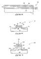
- Construction 20comprises the substrate 12 described above with reference to FIG. 1 .
- Construction 20also includes a dielectric material 22 comprising a laminate of three separate dielectric layers 24 , 26 and 28 .
- layers 24 , 26 and 28can comprise, consist essentially of, or consist of titanium oxide or cerium oxide.
- layers 24 and 28can each consist essentially of or consist of cerium oxide, while layer 26 consists essentially of or consists of titanium oxide.
- each of layers 24 and 28can consist essentially of or consist of titanium oxide, while layer 26 consists essentially of or consists of cerium oxide.
- layers 24 and 28consist essentially of or consist of cerium oxide while layer 26 consists essentially of or consists of titanium oxide, the laminate 22 will predominately comprise cerium oxide. In alternative embodiments where layers 24 and 28 consist essentially of or consist of titanium oxide while layer 26 consists essentially of or consists of cerium oxide, laminate 22 will predominately comprise titanium oxide.
- layers 24 and 28can be considered to comprise a first composition
- layer 26can be considered to comprise a second composition different from the first composition.
- One of the first and second compositionsis predominately titanium oxide, and the other is predominately cerium oxide.
- Layers 24 , 26 and 28can be considered to be a plurality of separate layers, with layers 24 and 28 being a pair of layers comprising a first composition, and which are otherwise adjacent except for the layer 26 of the second composition which is between them.
- the layers 24 , 26 and 28can each be deposited utilizing atomic layer deposition.
- the layerscan have any suitable thickness, and in particular aspects the individual layers will be atomic layer deposited to thicknesses of, for example, from about 10 ⁇ to about 50 ⁇ .
- the layer 26 comprising the second compositionis deposited over and in direct physical contact with the layer 24 comprising the first composition.
- one of the layers 26 and 24can consist essentially of, or consist of cerium oxide, and the other can consist essentially of or consist of titanium oxide.
- the inventionencompasses other aspects (not shown) in which dielectric materials other than cerium oxide and titanium oxide are incorporated into the laminate structure 22 .
- an intervening dielectric materialcan be provided between layers 26 and 28 so that a layer consisting essentially of or consisting of cerium oxide is spaced from a layer consisting essentially of or consisting of titanium oxide by an intervening dielectric material which does not contain either cerium oxide or titanium oxide.
- Such intervening dielectric materialcan comprise any suitable composition (such as, for example, silicon dioxide, silicon nitride, high k materials, etc.), and can be provided to, for example, adjust leakage properties of laminate 22 and/or adjust a dielectric constant of the laminate 22 .
- suitable compositionsuch as, for example, silicon dioxide, silicon nitride, high k materials, etc.
- laminate 22is shown to contain only three separate layers ( 24 , 26 and 28 ), it is to be understood that laminate 22 can be formed to comprise any suitable number of separate layers.
- Laminate 22can be described as comprising two or more separate layers, with at least two of the layers differing in composition relative to one another. At least one of layers of the laminate will typically predominately comprise cerium oxide, and at least one other layer of the laminate with typically predominately comprise titanium oxide.
- Construction 30comprises the substrate 12 described previously, and comprises the homogeneous dielectric material 14 described above with reference to FIG. 1 .
- Construction 30also comprises a laminate 32 over homogeneous material 14 , with such laminate comprising a first layer 34 and a second layer 36 .
- One of layers 34 and 36can predominately comprise, consist essentially of, or consist of cerium oxide, and the other can predominately comprise, consist essentially of, or consist of titanium oxide.
- the layers 34 and 36can be formed by any suitable methods, including, for example, ALD methods of the type described above with reference to FIG. 2 .
- homogeneous layer 14is thicker than either of the laminate layers 34 and 36 , and is approximately the same thickness as the combined thickness of laminate layers 34 and 36 . It is to be understood, however, that the invention encompasses other aspects in which multiple laminate layers are utilized to form a combined thickness of the laminate layers thicker than homogeneous material 14 , as well as aspects in which homogeneous material 14 is formed to be thicker than the combined thickness of the laminate materials provided thereover.
- An advantage to utilizing a homogeneous material 14 in combination with laminate layers 34 and 36is that such can enable tailoring of dielectric properties of the cerium oxide/titanium oxide material comprised by the combined layers 14 , 34 and 36 beyond the tailoring which can be achieved utilizing a homogeneous layer alone or utilizing the laminate layers alone.
- FIG. 4shows another construction 40 which illustrates yet another aspect of the invention.
- Construction 40comprises the substrate 12 , homogeneous material 14 , and laminate materials 34 and 36 described above with reference to FIG. 3 .
- the laminate materials 34 and 36are provided directly over substrate 12
- homogeneous material 14is provided over the laminate materials; which is the opposite ordering as the FIG. 3 embodiment.
- the shown embodiment of FIG. 4can be formed by, for example, atomic layer deposition of laminate layers 34 and 36 , followed by chemical vapor deposition of homogeneous material 14 .
- FIGS. 1-4can be incorporated into numerous circuit devices. Exemplary devices are described with reference to FIGS. 5-7 .
- a construction 50is illustrated to comprise a capacitor structure 52 over a semiconductor substrate 12 .
- Structure 52comprises a pair of capacitor electrodes 54 and 56 which are spaced from one another by a dielectric material 58 .
- Capacitor electrodes 54 and 56can comprise any suitable conductive material or combination of conductive materials, including, for example, metals (in either or both of elemental form and the form of metal compounds) and/or conductively-doped silicon.
- capacitor 52will be a metal-insulator-metal capacitor.
- Dielectric material 58can comprise a homogeneous mixture of cerium oxide and titanium oxide, and/or a laminate of cerium oxide and titanium oxide. Accordingly, dielectric material 58 can comprise, for example, any of the dielectric material structures described above with reference to FIGS. 1-4 .
- Capacitor electrode 54is diagrammatically illustrated as being electrically connected to adjacent circuitry 60 .
- Such adjacent circuitrycan comprise, for example, a transistor structure.
- the combination of a capacitor 52 with the transistor structurecan form a unit cell with of a dynamic random access memory (DRAM), and accordingly capacitor 52 can be incorporated into a DRAM array.
- Capacitor 52can also be incorporated into other types of electronic circuitry.
- circuitry 60can correspond to an analog circuit, a radio frequency circuit, a mixed signal integrated circuit, etc. Accordingly, capacitor 52 can be incorporated into an analog circuit, a radio frequency circuit, a mixed signal integrated circuit, etc.
- the dielectric material 58can comprise, consist essentially of, or consist of cerium oxide and titanium oxide.
- dielectric material 58will consist essentially of or consist of cerium oxide and titanium oxide.
- dielectric material 58will comprise a component consisting essentially of or consisting of titanium oxide in combination with cerium oxide, and another component which does not contain titanium oxide and cerium oxide.
- Such other componentcan be any suitable dielectric material for inclusion within the dielectric 58 of the capacitor construction 52 .
- capacitor dielectricswhich include either a homogeneous mixture of titanium oxide and cerium oxide and/or a laminate mixture of titanium oxide and cerium oxide, together with another component which is not a mixture of cerium oxide and titanium oxide (either homogeneous or laminate) can enable dielectric properties of the dielectric 58 to be tailored in ways which cannot be achieved utilizing mixtures of titanium oxide and cerium oxide alone.
- the other dielectric materials which can be utilized in addition to the mixtures of cerium oxide and titanium oxidecan comprise, consist essentially of, or consist of, for example, silicon dioxide, silicon nitride, or high-k dielectric materials.
- An exemplary method of forming capacitor construction 52is to provide the semiconductor substrate 12 , form the first electrode 54 over the substrate, form a combination of titanium oxide and cerium oxide over the first electrode as the dielectric material 58 (the combination can be a homogenous combination and/or a laminate), and then to form the second electrode 56 over the dielectric material.
- a construction 70illustrates a transistor device which can be formed in accordance with an aspect of the present invention.
- construction 70comprises a substrate 12 , and a transistor device 72 supported by such substrate.
- Transistor device 72comprises a pair of source/drain regions 74 extending within substrate 12 , and corresponding to conductively-doped diffusion regions.
- Transistor device 72further comprises a gate 76 formed over substrate 12 , and comprises a dielectric material 78 between gate 76 and substrate 12 .
- the transistor structurecomprises sidewall spacers 80 along sidewalls of gate 76 .
- Source/drain regions 74are spaced from one another by a channel region 82 which is beneath gate 76 .
- Dielectric material 78is between the gate and the channel region.
- Dielectric material 78can comprise any of the dielectric material constructions described previously with reference to FIGS. 1-4 . Accordingly, dielectric material 78 can comprise, consist essentially of, or consist of a mixture of cerium oxide and titanium oxide (either a homogeneous mixture, a laminate mixture, or a combination of a homogeneous mixture and a laminate mixture). Alternatively, dielectric 78 can comprise a mixture of cerium oxide and titanium oxide together with another dielectric which is not a mixture of cerium oxide and titanium oxide.
- Such other dielectriccan correspond to any suitable dielectric, including, for example, silicon dioxide, silicon nitride, or so-called high-k dielectric material.
- suitable dielectricincluding, for example, silicon dioxide, silicon nitride, or so-called high-k dielectric material.
- the utilization of the mixture of cerium oxide and titanium oxidecan allow the dielectric properties of dielectric material 78 to be tailored, and the inclusion of a dielectric material in addition to the mixture can further enable tailoring of the properties of dielectric material 78 .
- An exemplary method of forming transistor device 72is to provide the semiconductor substrate 12 , form the transistor device channel region 82 within the substrate, by, for example, appropriate doping of the substrate, form a combination of titanium oxide and cerium oxide over the channel region as the dielectric material 78 (the combination can be a homogenous combination and/or a laminate), and then to form gate 76 over the dielectric material.
- FIG. 7such shows a construction 100 comprising a read only memory (ROM) device (such as a flash memory device) 102 which can be formed in accordance with an exemplary aspect of the present invention.
- the read only memory device 102is supported by a substrate 12 .
- Read only memory device 102comprises a pair of source/drain regions 104 extending within substrate 12 .
- Source/drain regions 104correspond to conductively-doped diffusion regions.
- Device 102further comprises a gate stack 106 over the substrate.
- Gate stack 106comprises a floating gate 108 and a control gate 110 .
- Floating gate 108is separated from substrate 12 by a dielectric material 112
- floating gate 108is separated from control gate 110 by another dielectric material 114 .
- Dielectric material 112can be referred to as a tunnel dielectric (or tunnel gate insulator), and dielectric material 114 can be referred to as an inter-gate dielectric.
- a channel region 120extends between source/drain regions 104 , and floating gate 108 is separated from such channel region by the dielectric material 112 .
- Sidewall spacers 130are shown adjacent gate stack 106 , and along sidewalls of the gate stack. Sidewall spacers 130 can comprise any suitable dielectric material.
- Either or both of the dielectric materials 112 and 114 of the device 102can comprise a dielectric construction of the type described with reference to FIGS. 1-4 , and accordingly either or both of the dielectric materials 112 and 114 can comprise, consist essentially of, or consist of a mixture of cerium oxide and titanium oxide (either a homogeneous mixture, or a laminate mixture). Such mixture can be utilized alone as one or both of the dielectrics 112 and 114 , or can be utilized in combination with one or more other dielectric materials. For instance, either or both of the dielectric materials 112 or 114 can comprise a mixture of cerium oxide and titanium oxide, together with another dielectric which does not contain cerium oxide or titanium oxide.
- an advantage of utilizing a mixture of cerium oxide and titanium oxide with another dielectric which does not contain cerium oxide or titanium oxidecan be that the dielectric properties of the dielectric material can be better tailored than they could be if a mixture of titanium oxide and cerium oxide was utilized alone.
- FIGS. 5-7are exemplary embodiments for utilization of dielectric materials of the present invention.
- the mixed titanium oxide/cerium oxide dielectric materialscan be utilized in other devices, or in other embodiments of the shown devices.
- the flash memory device of FIG. 7can be a nitride read only memory (NROM) flash memory device in some aspects of the invention.
- the dielectric materials of FIGS. 1-4can be utilized in mixed signal integrated circuits, which are known in the art to be integrated circuits that process both analog and digital signals, such as, for example, disk drive read-channel integrated circuits.
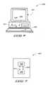
- FIG. 8illustrates generally, by way of example but not by way of limitation, an embodiment of a computer system 400 according to an aspect of the present invention.
- Computer system 400includes a monitor 401 or other communication output device, a keyboard 402 or other communication input device, and a motherboard 404 .
- Motherboard 404can carry a microprocessor 406 or other data processing unit, and at least one memory device 408 .
- Memory device 408can comprise various aspects of the invention described above.
- Memory device 408can comprise an array of memory cells, and such array can be coupled with addressing circuitry for accessing individual memory cells in the array. Further, the memory cell array can be coupled to a read circuit for reading data from the memory cells. The addressing and read circuitry can be utilized for conveying information between memory device 408 and processor 406 .
- FIG. 9Such is illustrated in the block diagram of the motherboard 404 shown in FIG. 9 .
- the addressing circuitryis illustrated as 410 and the read circuitry is illustrated as 412 .
- Various components of computer system 400can comprise one or more of the dielectric materials described previously in this disclosure.
- Processor device 406can correspond to a processor module, and associated memory utilized with the module can comprise teachings of the present invention.
- Memory device 408can correspond to a memory module.
- SIMMssingle in-line memory modules
- DIMMsdual in-line memory modules
- the memory devicecan be incorporated into any of a variety of designs which provide different methods of reading from and writing to memory cells of the device.
- One such methodis the page mode operation.
- Page mode operations in a DRAMare defined by the method of accessing a row of a memory cell arrays and randomly accessing different columns of the array. Data stored at the row and column intersection can be read and output while that column is accessed.
- EDOextended data output
- Memory device 408can comprise constructions formed in accordance with one or more aspects of the present invention.
- FIG. 10illustrates a simplified block diagram of a high-level organization of various embodiments of an exemplary electronic system 700 of the present invention.
- System 700can correspond to, for example, a computer system, a process control system, or any other system that employs a processor and associated memory.
- Electronic system 700has functional elements, including a processor or arithmetic/logic unit (ALU) 702 , a control unit 704 , a memory device unit 706 and an input/output (I/O) device 708 .
- ALUarithmetic/logic unit
- control unit 704controls the a memory device unit 706
- I/Oinput/output
- electronic system 700will have a native set of instructions that specify operations to be performed on data by the processor 702 and other interactions between the processor 702 , the memory device unit 706 and the I/O devices 708 .
- the control unit 704coordinates all operations of the processor 702 , the memory device 706 and the I/O devices 708 by continuously cycling through a set of operations that cause instructions to be fetched from the memory device 706 and executed.
- the memory device 706includes, but is not limited to, random access memory (RAM) devices, read-only memory (ROM) devices, and peripheral devices such as a floppy disk drive and a compact disk CD-ROM drive.
- RAMrandom access memory
- ROMread-only memory
- peripheral devicessuch as a floppy disk drive and a compact disk CD-ROM drive.
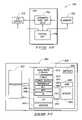
- FIG. 11is a simplified block diagram of a high-level organization of various embodiments of an exemplary electronic system 800 .
- the system 800includes a memory device 802 that has an array of memory cells 804 , address decoder 806 , row access circuitry 808 , column access circuitry 810 , read/write control circuitry 812 for controlling operations, and input/output circuitry 814 .
- the memory device 802further includes power circuitry 816 , and sensors 820 , such as current sensors for determining whether a memory cell is in a low-threshold conducting state or in a high-threshold non-conducting state.
- the illustrated power circuitry 816includes power supply circuitry 880 , circuitry 882 for providing a reference voltage, circuitry 884 for providing the first wordline with pulses, circuitry 886 for providing the second wordline with pulses, and circuitry 888 for providing the bitline with pulses.
- the system 800also includes a processor 822 , or memory controller for memory accessing.
- the memory device 802receives control signals from the processor 822 over wiring or metallization lines.
- the memory device 802is used to store data which is accessed via I/O lines. It will be appreciated by those skilled in the art that additional circuitry and control signals can be provided, and that the memory device 802 has been simplified to help focus on the invention.
- At least one of the processor 822 or memory device 802can include one or more constructions of the type described previously in this disclosure.
- Applications for memory cellscan include electronic systems for use in memory modules, device drivers, power modules, communication modems, processor modules, and application-specific modules, and may include multilayer, multichip modules.
- Such circuitrycan further be a subcomponent of a variety of electronic systems, such as a clock, a television, a cell phone, a personal computer, an automobile, an industrial control system, an aircraft, and others.
Landscapes
- Chemical & Material Sciences (AREA)
- Engineering & Computer Science (AREA)
- Materials Engineering (AREA)
- General Chemical & Material Sciences (AREA)
- Organic Chemistry (AREA)
- Metallurgy (AREA)
- Mechanical Engineering (AREA)
- Chemical Kinetics & Catalysis (AREA)
- Physics & Mathematics (AREA)
- Condensed Matter Physics & Semiconductors (AREA)
- Power Engineering (AREA)
- General Physics & Mathematics (AREA)
- Microelectronics & Electronic Packaging (AREA)
- Computer Hardware Design (AREA)
- Manufacturing & Machinery (AREA)
- Inorganic Chemistry (AREA)
- Semiconductor Memories (AREA)
Abstract
Description
Claims (5)
Priority Applications (2)
| Application Number | Priority Date | Filing Date | Title |
|---|---|---|---|
| US10/881,874US7323424B2 (en) | 2004-06-29 | 2004-06-29 | Semiconductor constructions comprising cerium oxide and titanium oxide |
| US11/064,163US7268035B2 (en) | 2004-06-29 | 2005-02-23 | Methods of forming semiconductor constructions comprising cerium oxide and titanium oxide |
Applications Claiming Priority (1)
| Application Number | Priority Date | Filing Date | Title |
|---|---|---|---|
| US10/881,874US7323424B2 (en) | 2004-06-29 | 2004-06-29 | Semiconductor constructions comprising cerium oxide and titanium oxide |
Related Child Applications (1)
| Application Number | Title | Priority Date | Filing Date |
|---|---|---|---|
| US11/064,163DivisionUS7268035B2 (en) | 2004-06-29 | 2005-02-23 | Methods of forming semiconductor constructions comprising cerium oxide and titanium oxide |
Publications (2)
| Publication Number | Publication Date |
|---|---|
| US20050285225A1 US20050285225A1 (en) | 2005-12-29 |
| US7323424B2true US7323424B2 (en) | 2008-01-29 |
Family
ID=35504650
Family Applications (2)
| Application Number | Title | Priority Date | Filing Date |
|---|---|---|---|
| US10/881,874Expired - LifetimeUS7323424B2 (en) | 2004-06-29 | 2004-06-29 | Semiconductor constructions comprising cerium oxide and titanium oxide |
| US11/064,163Expired - LifetimeUS7268035B2 (en) | 2004-06-29 | 2005-02-23 | Methods of forming semiconductor constructions comprising cerium oxide and titanium oxide |
Family Applications After (1)
| Application Number | Title | Priority Date | Filing Date |
|---|---|---|---|
| US11/064,163Expired - LifetimeUS7268035B2 (en) | 2004-06-29 | 2005-02-23 | Methods of forming semiconductor constructions comprising cerium oxide and titanium oxide |
Country Status (1)
| Country | Link |
|---|---|
| US (2) | US7323424B2 (en) |
Cited By (6)
| Publication number | Priority date | Publication date | Assignee | Title |
|---|---|---|---|---|
| US20060252211A1 (en)* | 2002-07-30 | 2006-11-09 | Micron Technology, Inc. | ATOMIC LAYER DEPOSITED NANOLAMINATES OF HfO2/ZrO2 FILMS AS GATE DIELECTRICS |
| US20070090441A1 (en)* | 2004-08-31 | 2007-04-26 | Micron Technology, Inc. | Titanium aluminum oxide films |
| US20070099366A1 (en)* | 2004-08-31 | 2007-05-03 | Micron Technology, Inc. | Lanthanum aluminum oxide dielectric layer |
| US20070158765A1 (en)* | 2006-01-10 | 2007-07-12 | Micron Technology, Inc. | Gallium lanthanide oxide films |
| US20090032910A1 (en)* | 2004-12-13 | 2009-02-05 | Micron Technology, Inc. | Dielectric stack containing lanthanum and hafnium |
| US20100207181A1 (en)* | 2006-02-16 | 2010-08-19 | Ahn Kie Y | Conductive layers for hafnium silicon oxynitride films |
Families Citing this family (29)
| Publication number | Priority date | Publication date | Assignee | Title |
|---|---|---|---|---|
| US6852167B2 (en) | 2001-03-01 | 2005-02-08 | Micron Technology, Inc. | Methods, systems, and apparatus for uniform chemical-vapor depositions |
| US7160577B2 (en) | 2002-05-02 | 2007-01-09 | Micron Technology, Inc. | Methods for atomic-layer deposition of aluminum oxides in integrated circuits |
| US7589029B2 (en) | 2002-05-02 | 2009-09-15 | Micron Technology, Inc. | Atomic layer deposition and conversion |
| US7135421B2 (en) | 2002-06-05 | 2006-11-14 | Micron Technology, Inc. | Atomic layer-deposited hafnium aluminum oxide |
| US6884739B2 (en) | 2002-08-15 | 2005-04-26 | Micron Technology Inc. | Lanthanide doped TiOx dielectric films by plasma oxidation |
| US7199023B2 (en) | 2002-08-28 | 2007-04-03 | Micron Technology, Inc. | Atomic layer deposited HfSiON dielectric films wherein each precursor is independendently pulsed |
| US7084078B2 (en) | 2002-08-29 | 2006-08-01 | Micron Technology, Inc. | Atomic layer deposited lanthanide doped TiOx dielectric films |
| US6958302B2 (en) | 2002-12-04 | 2005-10-25 | Micron Technology, Inc. | Atomic layer deposited Zr-Sn-Ti-O films using TiI4 |
| US7101813B2 (en) | 2002-12-04 | 2006-09-05 | Micron Technology Inc. | Atomic layer deposited Zr-Sn-Ti-O films |
| US7192892B2 (en) | 2003-03-04 | 2007-03-20 | Micron Technology, Inc. | Atomic layer deposited dielectric layers |
| US7135369B2 (en) | 2003-03-31 | 2006-11-14 | Micron Technology, Inc. | Atomic layer deposited ZrAlxOy dielectric layers including Zr4AlO9 |
| US7601649B2 (en) | 2004-08-02 | 2009-10-13 | Micron Technology, Inc. | Zirconium-doped tantalum oxide films |
| US7560395B2 (en) | 2005-01-05 | 2009-07-14 | Micron Technology, Inc. | Atomic layer deposited hafnium tantalum oxide dielectrics |
| US7687409B2 (en) | 2005-03-29 | 2010-03-30 | Micron Technology, Inc. | Atomic layer deposited titanium silicon oxide films |
| US7662729B2 (en) | 2005-04-28 | 2010-02-16 | Micron Technology, Inc. | Atomic layer deposition of a ruthenium layer to a lanthanide oxide dielectric layer |
| US7927948B2 (en) | 2005-07-20 | 2011-04-19 | Micron Technology, Inc. | Devices with nanocrystals and methods of formation |
| US7410910B2 (en) | 2005-08-31 | 2008-08-12 | Micron Technology, Inc. | Lanthanum aluminum oxynitride dielectric films |
| US7727908B2 (en) | 2006-08-03 | 2010-06-01 | Micron Technology, Inc. | Deposition of ZrA1ON films |
| US7563730B2 (en) | 2006-08-31 | 2009-07-21 | Micron Technology, Inc. | Hafnium lanthanide oxynitride films |
| US7776765B2 (en) | 2006-08-31 | 2010-08-17 | Micron Technology, Inc. | Tantalum silicon oxynitride high-k dielectrics and metal gates |
| US7759747B2 (en) | 2006-08-31 | 2010-07-20 | Micron Technology, Inc. | Tantalum aluminum oxynitride high-κ dielectric |
| US7605030B2 (en) | 2006-08-31 | 2009-10-20 | Micron Technology, Inc. | Hafnium tantalum oxynitride high-k dielectric and metal gates |
| US7432548B2 (en) | 2006-08-31 | 2008-10-07 | Micron Technology, Inc. | Silicon lanthanide oxynitride films |
| US7544604B2 (en) | 2006-08-31 | 2009-06-09 | Micron Technology, Inc. | Tantalum lanthanide oxynitride films |
| US20080087890A1 (en)* | 2006-10-16 | 2008-04-17 | Micron Technology, Inc. | Methods to form dielectric structures in semiconductor devices and resulting devices |
| US8367506B2 (en) | 2007-06-04 | 2013-02-05 | Micron Technology, Inc. | High-k dielectrics with gold nano-particles |
| US7759237B2 (en) | 2007-06-28 | 2010-07-20 | Micron Technology, Inc. | Method of forming lutetium and lanthanum dielectric structures |
| US20120309206A1 (en)* | 2011-04-22 | 2012-12-06 | Applied Materials, Inc. | Stoichiometry Control Of Transition Metal Oxides In Thin Films |
| TWI554636B (en)* | 2012-04-25 | 2016-10-21 | 應用材料股份有限公司 | Method for producing dielectric film from metal bismuth salt precursor |
Citations (16)
| Publication number | Priority date | Publication date | Assignee | Title |
|---|---|---|---|---|
| US6258654B1 (en)* | 1998-02-25 | 2001-07-10 | Sony Corporation | Method of manufacturing a semiconductor device |
| US6451647B1 (en)* | 2002-03-18 | 2002-09-17 | Advanced Micro Devices, Inc. | Integrated plasma etch of gate and gate dielectric and low power plasma post gate etch removal of high-K residual |
| US20020195683A1 (en)* | 1999-08-14 | 2002-12-26 | Kim Yeong-Kwan | Semiconductor device and method for manufacturing the same |
| US6509234B1 (en)* | 2002-02-21 | 2003-01-21 | Advanced Micro Devices, Inc. | Method of fabricating an ultra-thin fully depleted SOI device with T-shaped gate |
| US6528858B1 (en)* | 2002-01-11 | 2003-03-04 | Advanced Micro Devices, Inc. | MOSFETs with differing gate dielectrics and method of formation |
| US20040057193A1 (en) | 2002-09-19 | 2004-03-25 | Mr. Bum Ki Moon | Element Storage Layer in Integrated Circuits |
| US20040183116A1 (en) | 2000-08-11 | 2004-09-23 | Hag-Ju Cho | Integrated circuit devices having dielectric regions protected with multi-layer insulation structures and methods of fabricating same |
| US20040185613A1 (en)* | 2003-03-17 | 2004-09-23 | Taiwan Semiconductor Manufacturing Co. | Method of forming dram capacitors with protected outside crown surface for more robust structures |
| US6797567B2 (en)* | 2002-12-24 | 2004-09-28 | Macronix International Co., Ltd. | High-K tunneling dielectric for read only memory device and fabrication method thereof |
| US6812514B1 (en)* | 2002-09-16 | 2004-11-02 | Advanced Micro Devices, Inc. | High density floating gate flash memory and fabrication processes therefor |
| US6815297B1 (en)* | 2002-02-21 | 2004-11-09 | Advanced Micro Devices, Inc. | Ultra-thin fully depleted SOI device and method of fabrication |
| US20040235242A1 (en)* | 2003-05-20 | 2004-11-25 | Cem Basceri | Methods of forming capacitor constructions |
| US20050035410A1 (en)* | 2003-08-15 | 2005-02-17 | Yee-Chia Yeo | Semiconductor diode with reduced leakage |
| US6858514B2 (en)* | 2002-03-29 | 2005-02-22 | Sharp Laboratories Of America, Inc. | Low power flash memory cell and method |
| US20050224897A1 (en) | 2004-03-26 | 2005-10-13 | Taiwan Semiconductor Manufacturing Co., Ltd. | High-K gate dielectric stack with buffer layer to improve threshold voltage characteristics |
| US6995437B1 (en)* | 2003-03-05 | 2006-02-07 | Advanced Micro Devices, Inc. | Semiconductor device with core and periphery regions |
Family Cites Families (2)
| Publication number | Priority date | Publication date | Assignee | Title |
|---|---|---|---|---|
| KR100442104B1 (en)* | 2001-12-27 | 2004-07-27 | 삼성전자주식회사 | Method of fabricating semiconductor device having a capacitor |
| US20050224987A1 (en)* | 2004-04-07 | 2005-10-13 | Hortaleza Edgardo R | Structure and method for contact pads having double overcoat-protected bondable metal plugs over copper-metallized integrated circuits |
- 2004
- 2004-06-29USUS10/881,874patent/US7323424B2/ennot_activeExpired - Lifetime
- 2005
- 2005-02-23USUS11/064,163patent/US7268035B2/ennot_activeExpired - Lifetime
Patent Citations (16)
| Publication number | Priority date | Publication date | Assignee | Title |
|---|---|---|---|---|
| US6258654B1 (en)* | 1998-02-25 | 2001-07-10 | Sony Corporation | Method of manufacturing a semiconductor device |
| US20020195683A1 (en)* | 1999-08-14 | 2002-12-26 | Kim Yeong-Kwan | Semiconductor device and method for manufacturing the same |
| US20040183116A1 (en) | 2000-08-11 | 2004-09-23 | Hag-Ju Cho | Integrated circuit devices having dielectric regions protected with multi-layer insulation structures and methods of fabricating same |
| US6528858B1 (en)* | 2002-01-11 | 2003-03-04 | Advanced Micro Devices, Inc. | MOSFETs with differing gate dielectrics and method of formation |
| US6815297B1 (en)* | 2002-02-21 | 2004-11-09 | Advanced Micro Devices, Inc. | Ultra-thin fully depleted SOI device and method of fabrication |
| US6509234B1 (en)* | 2002-02-21 | 2003-01-21 | Advanced Micro Devices, Inc. | Method of fabricating an ultra-thin fully depleted SOI device with T-shaped gate |
| US6451647B1 (en)* | 2002-03-18 | 2002-09-17 | Advanced Micro Devices, Inc. | Integrated plasma etch of gate and gate dielectric and low power plasma post gate etch removal of high-K residual |
| US6858514B2 (en)* | 2002-03-29 | 2005-02-22 | Sharp Laboratories Of America, Inc. | Low power flash memory cell and method |
| US6812514B1 (en)* | 2002-09-16 | 2004-11-02 | Advanced Micro Devices, Inc. | High density floating gate flash memory and fabrication processes therefor |
| US20040057193A1 (en) | 2002-09-19 | 2004-03-25 | Mr. Bum Ki Moon | Element Storage Layer in Integrated Circuits |
| US6797567B2 (en)* | 2002-12-24 | 2004-09-28 | Macronix International Co., Ltd. | High-K tunneling dielectric for read only memory device and fabrication method thereof |
| US6995437B1 (en)* | 2003-03-05 | 2006-02-07 | Advanced Micro Devices, Inc. | Semiconductor device with core and periphery regions |
| US20040185613A1 (en)* | 2003-03-17 | 2004-09-23 | Taiwan Semiconductor Manufacturing Co. | Method of forming dram capacitors with protected outside crown surface for more robust structures |
| US20040235242A1 (en)* | 2003-05-20 | 2004-11-25 | Cem Basceri | Methods of forming capacitor constructions |
| US20050035410A1 (en)* | 2003-08-15 | 2005-02-17 | Yee-Chia Yeo | Semiconductor diode with reduced leakage |
| US20050224897A1 (en) | 2004-03-26 | 2005-10-13 | Taiwan Semiconductor Manufacturing Co., Ltd. | High-K gate dielectric stack with buffer layer to improve threshold voltage characteristics |
Non-Patent Citations (11)
| Title |
|---|
| Becht, M. et al., "Some Cerium beta-Diketonate Derivatives as MOCVD Precursors", Chem. Mater., vol. 5, No. 1, 1993, pp. 137-144. |
| Kukli, K. et al., "Atomic Layer Deposition of Titanium Oxide from Til<SUB>4 </SUB>and H<SUB>2</SUB>O<SUB>2</SUB>", Chem. Vap. Deposition, vol. 6, No. 6, 2000, pp. 303-310. |
| McKee, R. et al., "Crystalline Oxides on Silicon: The First Five Monolayers", Physical Review Letters, vol. 81, No. 14, Oct. 5, 1998, pp. 3014-3017. |
| McKee, R. et al., "Physical Structure and Inversion Charge at a Semiconductor Interface with a Crystalline Oxide", http://www.sciencemag.org/cgi/content/full/293/5529/468, reprinted Jul. 16, 2002, 9 pages. |
| Mölsä, H. et al., "Deposition of Cerium Dioxide Thin Films on Silicon Substrates by Atomic Layer Epitaxy", Mat. Res. Soc. Symp. Proc., vol. 335, 1994 Materials Research Society, pp. 341-350. |
| Nishikawa, Y. et al., "Electrical Properties of Single Crystalline CeO<SUB>2 </SUB>High-k Dielectrics Directly Grown on Si (111)", Jpn. J. Appl. Phys., vol. 41, Part 1, No. 4B, Apr. 2002, pp. 2480-2483. |
| Osten, H. et al., "High-k Gate Dielectrics with Ultra-Low Leakage Current Based on Praseodymum Oxide", IEEE Apr. 2000, pp. 653-656. |
| Sneh, O. et al., "Thin Film Atomic Layer Deposition Equipment for Semiconductor Processing", Thin Solid Films 402 (2002), pp. 248-261. |
| Wilk, G. et al., "High-k Gate Dielectrics: Current Status and Materials Properties Considerations", Jour. App. Phys., vol. 89, No. 10, May 15, 2001, pp. 5243-5275. |
| Wu, Y. et al., "Electrical Characteristics of High Quality La<SUB>2</SUB>O<SUB>3 </SUB>Gate Dielectric with Equivalent Oxide Thickness of 5 A", IEEE vol. 21, No. 7, Jul. 2000, pp. 341-343. |
| Zhang, H . et al., "Atomic Layer Deposition of High Dielectric Constant Nanolaminates", J. of the Electrochemical Soc., vol. 148, No. 4, 2001, pp. F63-F66. |
Cited By (17)
| Publication number | Priority date | Publication date | Assignee | Title |
|---|---|---|---|---|
| US20060252211A1 (en)* | 2002-07-30 | 2006-11-09 | Micron Technology, Inc. | ATOMIC LAYER DEPOSITED NANOLAMINATES OF HfO2/ZrO2 FILMS AS GATE DIELECTRICS |
| US8154066B2 (en) | 2004-08-31 | 2012-04-10 | Micron Technology, Inc. | Titanium aluminum oxide films |
| US20070090441A1 (en)* | 2004-08-31 | 2007-04-26 | Micron Technology, Inc. | Titanium aluminum oxide films |
| US20070099366A1 (en)* | 2004-08-31 | 2007-05-03 | Micron Technology, Inc. | Lanthanum aluminum oxide dielectric layer |
| US8541276B2 (en) | 2004-08-31 | 2013-09-24 | Micron Technology, Inc. | Methods of forming an insulating metal oxide |
| US8237216B2 (en) | 2004-08-31 | 2012-08-07 | Micron Technology, Inc. | Apparatus having a lanthanum-metal oxide semiconductor device |
| US7867919B2 (en) | 2004-08-31 | 2011-01-11 | Micron Technology, Inc. | Method of fabricating an apparatus having a lanthanum-metal oxide dielectric layer |
| US20110037117A1 (en)* | 2004-08-31 | 2011-02-17 | Ahn Kie Y | Lanthanum-metal oxide dielectric apparatus, methods, and systems |
| US20090032910A1 (en)* | 2004-12-13 | 2009-02-05 | Micron Technology, Inc. | Dielectric stack containing lanthanum and hafnium |
| US7915174B2 (en) | 2004-12-13 | 2011-03-29 | Micron Technology, Inc. | Dielectric stack containing lanthanum and hafnium |
| US7972974B2 (en) | 2006-01-10 | 2011-07-05 | Micron Technology, Inc. | Gallium lanthanide oxide films |
| US20070158765A1 (en)* | 2006-01-10 | 2007-07-12 | Micron Technology, Inc. | Gallium lanthanide oxide films |
| US9129961B2 (en) | 2006-01-10 | 2015-09-08 | Micron Technology, Inc. | Gallium lathanide oxide films |
| US9583334B2 (en) | 2006-01-10 | 2017-02-28 | Micron Technology, Inc. | Gallium lanthanide oxide films |
| US8067794B2 (en) | 2006-02-16 | 2011-11-29 | Micron Technology, Inc. | Conductive layers for hafnium silicon oxynitride films |
| US20100207181A1 (en)* | 2006-02-16 | 2010-08-19 | Ahn Kie Y | Conductive layers for hafnium silicon oxynitride films |
| US8785312B2 (en) | 2006-02-16 | 2014-07-22 | Micron Technology, Inc. | Conductive layers for hafnium silicon oxynitride |
Also Published As
| Publication number | Publication date |
|---|---|
| US7268035B2 (en) | 2007-09-11 |
| US20050285103A1 (en) | 2005-12-29 |
| US20050285225A1 (en) | 2005-12-29 |
Similar Documents
| Publication | Publication Date | Title |
|---|---|---|
| US7323424B2 (en) | Semiconductor constructions comprising cerium oxide and titanium oxide | |
| US7405454B2 (en) | Electronic apparatus with deposited dielectric layers | |
| US6893984B2 (en) | Evaporated LaA1O3 films for gate dielectrics | |
| US7217630B2 (en) | Methods of forming hafnium oxide | |
| US7199023B2 (en) | Atomic layer deposited HfSiON dielectric films wherein each precursor is independendently pulsed | |
| US7554161B2 (en) | HfAlO3 films for gate dielectrics | |
| US7045430B2 (en) | Atomic layer-deposited LaAlO3 films for gate dielectrics | |
| TWI389207B (en) | Capacitor, dielectric structure and method of forming dielectric structure | |
| US20070026601A1 (en) | Dram constructions and electronic systems | |
| US20060255470A1 (en) | ZrAlxOy DIELECTRIC LAYERS | |
| US8497566B2 (en) | Capacitors including conductive TiOxNx | |
| KR20100093353A (en) | Semiconductor device and fabficating method the sameof | |
| US7439564B2 (en) | Methods of forming capacitor constructions | |
| KR20250060792A (en) | Semiconductor device, memory device and method of manufacturing semiconductor device |
Legal Events
| Date | Code | Title | Description |
|---|---|---|---|
| AS | Assignment | Owner name:MICRON TECHNOLOGY, INC., IDAHO Free format text:ASSIGNMENT OF ASSIGNORS INTEREST;ASSIGNORS:AHN, KIE Y.;FORBES, LEONARD;REEL/FRAME:015537/0299;SIGNING DATES FROM 20040618 TO 20040621 | |
| FEPP | Fee payment procedure | Free format text:PAYOR NUMBER ASSIGNED (ORIGINAL EVENT CODE: ASPN); ENTITY STATUS OF PATENT OWNER: LARGE ENTITY | |
| STCF | Information on status: patent grant | Free format text:PATENTED CASE | |
| FPAY | Fee payment | Year of fee payment:4 | |
| FPAY | Fee payment | Year of fee payment:8 | |
| AS | Assignment | Owner name:U.S. BANK NATIONAL ASSOCIATION, AS COLLATERAL AGENT, CALIFORNIA Free format text:SECURITY INTEREST;ASSIGNOR:MICRON TECHNOLOGY, INC.;REEL/FRAME:038669/0001 Effective date:20160426 Owner name:U.S. BANK NATIONAL ASSOCIATION, AS COLLATERAL AGEN Free format text:SECURITY INTEREST;ASSIGNOR:MICRON TECHNOLOGY, INC.;REEL/FRAME:038669/0001 Effective date:20160426 | |
| AS | Assignment | Owner name:MORGAN STANLEY SENIOR FUNDING, INC., AS COLLATERAL AGENT, MARYLAND Free format text:PATENT SECURITY AGREEMENT;ASSIGNOR:MICRON TECHNOLOGY, INC.;REEL/FRAME:038954/0001 Effective date:20160426 Owner name:MORGAN STANLEY SENIOR FUNDING, INC., AS COLLATERAL Free format text:PATENT SECURITY AGREEMENT;ASSIGNOR:MICRON TECHNOLOGY, INC.;REEL/FRAME:038954/0001 Effective date:20160426 | |
| AS | Assignment | Owner name:U.S. BANK NATIONAL ASSOCIATION, AS COLLATERAL AGENT, CALIFORNIA Free format text:CORRECTIVE ASSIGNMENT TO CORRECT THE REPLACE ERRONEOUSLY FILED PATENT #7358718 WITH THE CORRECT PATENT #7358178 PREVIOUSLY RECORDED ON REEL 038669 FRAME 0001. ASSIGNOR(S) HEREBY CONFIRMS THE SECURITY INTEREST;ASSIGNOR:MICRON TECHNOLOGY, INC.;REEL/FRAME:043079/0001 Effective date:20160426 Owner name:U.S. BANK NATIONAL ASSOCIATION, AS COLLATERAL AGEN Free format text:CORRECTIVE ASSIGNMENT TO CORRECT THE REPLACE ERRONEOUSLY FILED PATENT #7358718 WITH THE CORRECT PATENT #7358178 PREVIOUSLY RECORDED ON REEL 038669 FRAME 0001. ASSIGNOR(S) HEREBY CONFIRMS THE SECURITY INTEREST;ASSIGNOR:MICRON TECHNOLOGY, INC.;REEL/FRAME:043079/0001 Effective date:20160426 | |
| AS | Assignment | Owner name:JPMORGAN CHASE BANK, N.A., AS COLLATERAL AGENT, ILLINOIS Free format text:SECURITY INTEREST;ASSIGNORS:MICRON TECHNOLOGY, INC.;MICRON SEMICONDUCTOR PRODUCTS, INC.;REEL/FRAME:047540/0001 Effective date:20180703 Owner name:JPMORGAN CHASE BANK, N.A., AS COLLATERAL AGENT, IL Free format text:SECURITY INTEREST;ASSIGNORS:MICRON TECHNOLOGY, INC.;MICRON SEMICONDUCTOR PRODUCTS, INC.;REEL/FRAME:047540/0001 Effective date:20180703 | |
| AS | Assignment | Owner name:MICRON TECHNOLOGY, INC., IDAHO Free format text:RELEASE BY SECURED PARTY;ASSIGNOR:U.S. BANK NATIONAL ASSOCIATION, AS COLLATERAL AGENT;REEL/FRAME:047243/0001 Effective date:20180629 | |
| MAFP | Maintenance fee payment | Free format text:PAYMENT OF MAINTENANCE FEE, 12TH YEAR, LARGE ENTITY (ORIGINAL EVENT CODE: M1553); ENTITY STATUS OF PATENT OWNER: LARGE ENTITY Year of fee payment:12 | |
| AS | Assignment | Owner name:MICRON TECHNOLOGY, INC., IDAHO Free format text:RELEASE BY SECURED PARTY;ASSIGNOR:MORGAN STANLEY SENIOR FUNDING, INC., AS COLLATERAL AGENT;REEL/FRAME:050937/0001 Effective date:20190731 | |
| AS | Assignment | Owner name:MICRON TECHNOLOGY, INC., IDAHO Free format text:RELEASE BY SECURED PARTY;ASSIGNOR:JPMORGAN CHASE BANK, N.A., AS COLLATERAL AGENT;REEL/FRAME:051028/0001 Effective date:20190731 Owner name:MICRON SEMICONDUCTOR PRODUCTS, INC., IDAHO Free format text:RELEASE BY SECURED PARTY;ASSIGNOR:JPMORGAN CHASE BANK, N.A., AS COLLATERAL AGENT;REEL/FRAME:051028/0001 Effective date:20190731 |