US7322754B2 - Compact optical sub-assembly - Google Patents
Compact optical sub-assemblyDownload PDFInfo
- Publication number
- US7322754B2 US7322754B2US11/054,453US5445305AUS7322754B2US 7322754 B2US7322754 B2US 7322754B2US 5445305 AUS5445305 AUS 5445305AUS 7322754 B2US7322754 B2US 7322754B2
- Authority
- US
- United States
- Prior art keywords
- laser
- light
- optical
- detector
- axis
- Prior art date
- Legal status (The legal status is an assumption and is not a legal conclusion. Google has not performed a legal analysis and makes no representation as to the accuracy of the status listed.)
- Active, expires
Links
- 230000003287optical effectEffects0.000titleclaimsabstractdescription91
- 230000001154acute effectEffects0.000claimsabstractdescription6
- 239000000919ceramicSubstances0.000claimsdescription24
- 230000005540biological transmissionEffects0.000claimsdescription20
- 239000013307optical fiberSubstances0.000claimsdescription10
- 239000010409thin filmSubstances0.000claimsdescription4
- XUIMIQQOPSSXEZ-UHFFFAOYSA-NSiliconChemical compound[Si]XUIMIQQOPSSXEZ-UHFFFAOYSA-N0.000abstractdescription2
- 229910052710siliconInorganic materials0.000abstractdescription2
- 239000010703siliconSubstances0.000abstractdescription2
- 229910000679solderInorganic materials0.000description5
- 238000013461designMethods0.000description4
- 239000000835fiberSubstances0.000description4
- 230000005693optoelectronicsEffects0.000description4
- 238000012546transferMethods0.000description4
- 235000011449RosaNutrition0.000description3
- 239000000463materialSubstances0.000description3
- 230000008054signal transmissionEffects0.000description3
- MCMNRKCIXSYSNV-UHFFFAOYSA-NZirconium dioxideChemical compoundO=[Zr]=OMCMNRKCIXSYSNV-UHFFFAOYSA-N0.000description2
- 238000013459approachMethods0.000description2
- 230000003247decreasing effectEffects0.000description2
- 238000010586diagramMethods0.000description2
- 230000010354integrationEffects0.000description2
- 238000004519manufacturing processMethods0.000description2
- 238000012544monitoring processMethods0.000description2
- 239000000243solutionSubstances0.000description2
- RYGMFSIKBFXOCR-UHFFFAOYSA-NCopperChemical compound[Cu]RYGMFSIKBFXOCR-UHFFFAOYSA-N0.000description1
- 241000510009Varanus griseusSpecies0.000description1
- 238000000429assemblyMethods0.000description1
- 229910052797bismuthInorganic materials0.000description1
- JCXGWMGPZLAOME-UHFFFAOYSA-Nbismuth atomChemical compound[Bi]JCXGWMGPZLAOME-UHFFFAOYSA-N0.000description1
- 239000003990capacitorSubstances0.000description1
- 239000004020conductorSubstances0.000description1
- 238000010276constructionMethods0.000description1
- 229910052802copperInorganic materials0.000description1
- 239000010949copperSubstances0.000description1
- 238000005530etchingMethods0.000description1
- 238000002347injectionMethods0.000description1
- 239000007924injectionSubstances0.000description1
- 229910000833kovarInorganic materials0.000description1
- 229910052751metalInorganic materials0.000description1
- 239000002184metalSubstances0.000description1
- 238000000034methodMethods0.000description1
- 238000004806packaging method and processMethods0.000description1
- 230000001902propagating effectEffects0.000description1
- 238000005476solderingMethods0.000description1
- 239000007787solidSubstances0.000description1
- XSOKHXFFCGXDJZ-UHFFFAOYSA-Ntelluride(2-)Chemical compound[Te-2]XSOKHXFFCGXDJZ-UHFFFAOYSA-N0.000description1
Images


Classifications
- G—PHYSICS
- G02—OPTICS
- G02B—OPTICAL ELEMENTS, SYSTEMS OR APPARATUS
- G02B6/00—Light guides; Structural details of arrangements comprising light guides and other optical elements, e.g. couplings
- G02B6/24—Coupling light guides
- G02B6/42—Coupling light guides with opto-electronic elements
- G02B6/4201—Packages, e.g. shape, construction, internal or external details
- G02B6/4204—Packages, e.g. shape, construction, internal or external details the coupling comprising intermediate optical elements, e.g. lenses, holograms
- G02B6/4214—Packages, e.g. shape, construction, internal or external details the coupling comprising intermediate optical elements, e.g. lenses, holograms the intermediate optical element having redirecting reflective means, e.g. mirrors, prisms for deflecting the radiation from horizontal to down- or upward direction toward a device
- G—PHYSICS
- G02—OPTICS
- G02B—OPTICAL ELEMENTS, SYSTEMS OR APPARATUS
- G02B6/00—Light guides; Structural details of arrangements comprising light guides and other optical elements, e.g. couplings
- G02B6/24—Coupling light guides
- G02B6/42—Coupling light guides with opto-electronic elements
- G02B6/4201—Packages, e.g. shape, construction, internal or external details
- G02B6/4246—Bidirectionally operating package structures
Definitions
- the present inventionrelates to a compact optical sub-assembly (OSA), and in particular to a transmitter optical sub-assembly (TOSA) including a light source mounted at an angle to the output axis.
- OSAcompact optical sub-assembly
- TOSAtransmitter optical sub-assembly
- the driving forces in the transceiver manufacturing industryare reducing the form factor sizes, increasing the data transfer rates, and decreasing the costs.
- the conventional butterfly-type or transistor outline (TO)can design approach must be replaced with a more exotic component packaging approach.
- the OSAmust use controlled impedance connections for the high speed RF electrical signal path between the OSA chip and the transceiver electronics.
- the total number of component partsmust be reduced, and manufacturable from readily available materials.
- the assembly processes, including optical alignment,must be simplified and/or automated to reduce labor costs and increase production rates, and the fiber receptacle components should support a variety of wavelengths.
- OSA designssuch as the one disclosed in U.S. Pat. No. 5,537,504, issued Jul. 16, 1996 to Cina et al and assigned to the present Applicant, include a opto-electronic (O/E) transducer 4 mounted in a container 25 , which is sealed by a window 26 .
- Solid metallic leads 23 and 24extend through the rear of the container 25 for soldering to other electrical leads or directly to a transceiver PCB.
- the Cina et al devicewill suffer from poor signal integrity at high data transfer rates, because the RF signals need to transmit through the leads 23 and 24 , which limits the quality of the transmission and the positioning of the transceiver PCB.
- the use of flexible-tape conductive wiringhas been disclosed in U.S.
- An object of the present inventionis to overcome the shortcomings of the prior art by providing an optical sub-assembly with a controlled signal impedance between the transducer chip and the transceiver PCB.
- Another object of the present inventionis to maximize functionality, while minimizing the size of the transducer chip to conform to small form factor design restrictions.
- the present inventionrelates to a transmitter optical sub-assembly, for converting an electrical data signal into an optical data signal, comprising:
- FIG. 1is a cross-sectional isometric view of a transmitter optical sub-assembly (TOSA) according to the present invention
- FIG. 2is an isometric view of the housing of the TOSA of FIG. 1 ;
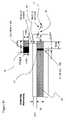
- FIG. 3is an exploded isometric view of the ceramic feedthrough of the TOSA of FIG. 1 ;
- FIG. 4is a top view of the TOSA of FIG. 1 with a housing cover removed;
- FIG. 5is a top view of the internal optics and electronics of the TOSA of FIGS. 1 and 4 ;
- FIG. 6is a top view of the optical bench of the TOSA of FIGS. 1 , 4 and 5 ;
- FIG. 7is a side view of the rear beam steering arrangement for directing light to the monitor photo-detector
- FIG. 8is a top view of the highlighted section of the optical bench of FIG. 4 ;
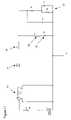
- FIG. 9is a circuit diagram of the TOSA of FIGS. 1 and 2 ;
- FIG. 10is a top view of the integrated resistances of the optical bench of FIGS. 8 and 9 ;
- FIG. 11is an alternative circuit diagram of the TOSA of FIGS. 1 and 2 ;
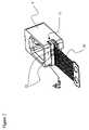
- FIG. 12is an isometric view of the TOSA of FIGS. 1 and 4 mounted in an optical transceiver.
- a transmitter optical sub-assemblyincludes an optical coupler 2 , a main housing 3 , and an electrical connector 4 .
- the optical coupler 2defines a bore 6 with a zirconia split sleeve 7 therein for receiving an optical fiber ferrule mounted on the end of an optical fiber, preferably fitted into an LC optical connector, as is well known in the art.
- An angle polished ferrule 8is mounted in the optical coupler 2 for transmitting light from the housing to the optical fiber along a main optical axis OA.
- the main housing 3is comprised of a metal injection molded (MIM) hermetic package 9 with a lid 11 , comprised of a material with a relatively low coefficient of thermal expansion, e.g. Kovar, although any suitable construction method and material can be used.
- a focusing lens 12hermetically seals the front or optical end of the housing 3 , while a multi-layer ceramic electrical feedthrough 13 hermetically seals the back or electrical end thereof.
- a opto-electronic transducer, in the form of a laser assemblycomprising a laser 14 , e.g. an externally modulated optical cavity laser (EML) diode, and a modulator 15 is mounted on a silicon optical bench 16 within the main housing 3 .
- An optical isolator 17is positioned between the focusing lens 12 and the laser 14 to prevent light from the optical fiber from entering the laser 14 .
- a thermal electronic cooler (TEC) 18preferably constructed of an array of bismuth telluride (BiTe) elements sandwiched between two pieces of ceramic, is positioned underneath the optical bench 16 .
- the TEC 18is included to cool or maintain the laser 14 at a predetermined fixed operating temperature.
- performanceis enhanced and optical signals can be transmitted over extended fiber distances, e.g. more than 100 km.
- the operating wavelength of the laser 14is stabilized and the modulated wavelength variation (chirp) is reduced.
- a temperature stabilized laseralso has less variation in electrical to optical transfer characteristic reducing the modulation requirements of the laser driver electronics.
- the illustrated embodimenttakes the form of a cooled TOSA
- similar uncooled TOSA devicescould also be constructed in this form factor, possibly with the inclusion of a driver chip as integration advances.
- This configurationwould be well suited to heatsink the thermal energy produced by laser driver integrated circuits.
- this form factorcould be used to integrate wavelength locking functions, needed for dense wavelength division multiplexing (DWDM) applications, into a transceiver device.
- DWDMdense wavelength division multiplexing
- the multi-layer ceramic feed-through 13includes five main ceramic layers 131 to 135 , which provide low inductance ground connections, an RF ground reference plane, and micro-strip signal transmission structures for propagating high speed RF data signals to the laser 14 .
- the middle layer 133includes an array of conductive traces 19 a to 19 i , six of which 19 a , 19 b , and 19 f to 19 i provide power, control and monitoring function for the various components on the optical bench 16 , e.g. monitor photo-detector and thermistor.
- Traces 19 c and 19 eare ground traces for high frequency signal trace 19 d .
- Conductive vias 20extend downwardly from traces 19 c and 19 e for connection with a first ground plane 21 formed on the second ceramic layer 132 between the first and second ceramic layers 131 and 132 , respectively.
- Castellations 22formed in the back of the first to fourth ceramic layers 131 to 135 extend from the first ground layer 21 upwardly to a second ground layer 23 formed on the fourth ceramic layer 134 between the fourth and fifth ceramic layers 134 and 135 , respectively.
- the width of the signal trace 19 d , the spacing between the signal trace 19 d and the ground traces 19 c and 19 e , and the thicknesses of the third and fourth ceramic layers 134 and 135are designed to provide a desired impedance, e.g.
- Additional ceramic layerscan be provided between the third and fourth layers 133 and 134 and between the second and third layers 132 and 133 to achieve a desired thickness.
- the top and bottom of the first and fifth ceramic layers 131 and 135 , respectively,are metalized and brazed to the housing 9 .
- the electrical connector 4includes a multi-layer flexible circuit, referred to as a micro-strip transmission line, which a signal layer, a ground layer and a mask layer.
- the signal layerincludes two RF data signal transmission lines, two or more ground lines, and four or more control lines.
- One end of the RF data signal transmission linesare connected to RF data signal pads on the ceramic feed-through 13 , using BGA solder balls or other suitable means.
- solder balls or other suitable meansare used to connect one end of the control lines to control pads on the ceramic feed-through 13 , while one end of the ground lines is connected to ground connection pads on the ceramic feed-through 13 .
- the other ends of the linesinclude solder pads for connection to the transceiver PCB.
- the ground layerincludes openings enabling access to the control lines, as well for the RF data signal lines.
- the ground linesare connected to the ground layer at various points.
- the mask layerprovides a solder mask or cover for the copper ground layer, and includes a plurality of openings enabling access to the solder pads on the bottom of the ceramic feed-through 13 .
- a lead-frame electrical interconnect 24can be used with or in place of the flexible circuit 4 for connecting the ceramic feed-through 13 with a PCB in the host transceiver device. When used together the electrical interconnect 24 is trimmed, soldered to the flexible circuit 4 , and bent into the configuration of FIG. 1 .
- FIG. 5illustrates opto-electronic components 25 highlighted in FIG. 4 .
- the EML laser 14is defined by a laser cavity, which generates light and launches a beam of light along a laser axis LA into the modulator 15 .
- the laser axis LAis disposed along the main optical axis OA; however, to limit the amount of light reflecting from the modulator/air interface and back into the laser cavity, the laser axis LA according to the present invention is positioned at an acute angle, e.g.
- ⁇25° to 45°, preferably 33°, from the main optical axis OA
- the modulator 15is curved for redirecting the beam of light from traveling along the laser axis LA to traveling along the main optical axis OA, whereby the beam of light will travel through a collimating lens 26 and the optical isolator 17 to the focusing lens 12 and out through the optical coupler 2 to an optical fiber therein.
- a lens or some other optic devicecould redirect the beam of light from the laser axis LA to the optical axis OA.
- a monitor photo-detectore.g. photodiode 27
- a rear beam steering lens 28is provided for redirecting the monitor light from the laser axis LA to a photodiode axis parallel to the main optical axis OA.
- the photodiode axiscould also be at a slight angle to the main optical axis OA in accordance with other alignment requirements, as long as the monitor light is tilted towards the main optical axis OA to save space on the optical bench 16 . As best seen in FIG.
- the rear beam steering lens 28is mounted in a cavity 29 in the optical bench 16 and directs the monitor light downwardly into a v-groove trench 30 etched from the optical bench 16 and extending from the cavity 29 .
- a reflective surface 31is provided at the end of the trench 30 for redirecting the monitor light onto the photodiode 27 , which is positioned face down over the trench 30 .
- the rear beam steering lens 28also focuses the monitor light onto photodiode 27 , thereby increasing the monitor current and decreasing noise.
- monitor photodiodeswould be mounted vertically directly behind the rear facet, which in accordance with the present invention would place the monitor photodiode along the laser axis LA.
- the industry standard spacing for a small form factor LC duplex fiber connectoris 6.25 mm between the transmit and receive optical ports; therefore, the width of the housing 3 must be less than 6 mm to ensure proper spacing between the ROSA and the TOSA. Accordingly, positioning the monitor photodiode 27 along the laser axis LA would cause this critical dimension to be exceeded.
- etching the trench 30 with the reflective surface 31 along the laser axis LAwould be much more difficult, requiring a much larger etch, since they are not along the optical bench's crystalline plane.
- Other opto-electronic elements mounted on the optical bench 16include a thermistor 33 for measuring the temperature of the laser 14 , and a capacitor 34 defining a high bias filter used as a high frequency bias choke.
- a co-planar transmission line 35is integrated into the optical bench 16 for transmitting RF signals to the laser assembly, i.e. modulator 15 .
- the transmission line 35includes a thin film resistor 36 integrated into the optical bench 16 adjacent to the transmission line 35 for providing an resistance in parallel with the transmission line 35 to match the impedance of the transmission line 35 with that of the laser assembly.
- An additional thin film resistor 37is integrated into the transmission line 35 providing series resistance for reducing microwave reflections at relatively high frequencies, e.g. above 5 GHz.
- a bond wire 38( FIG. 10 ) is used to connect the transmission line 35 and the parallel resistor 36 , the inductance of which is represented by Lp in FIG. 9 .
- a bond wire 39is used to connect the transmission line 35 and the laser assembly, i.e. modulator 15 , the inductance of which is represent by Ls in FIG. 9 .
- V 1represents an external power source
- T 1represents the transmission line 35 .
- C 1 , C 2 , R 4 and R 5represent the equivalent capacitance and resistance of the modulator 15 .
- both bond wires 38 and 39 for the parallel resistor 36 and the series resistor 37can be connected to the modulator, thereby minimizing microwave reflection.
- FIG. 12illustrates the TOSA 1 , in accordance with the present invention, mounted in a small form factor optical transceiver housing 51 adjacent to a ROSA 52 .
- the transceiver housing 51includes an LC optical coupler 53 (or other suitable coupler) on a front end thereof, with an electrical connector extending from another end 54 thereof.
- a printed circuit boardis mounted within the housing 51 providing control and monitoring circuitry for both the TOSA 1 and the ROSA 52 .
Landscapes
- Physics & Mathematics (AREA)
- General Physics & Mathematics (AREA)
- Optics & Photonics (AREA)
- Optical Couplings Of Light Guides (AREA)
- Semiconductor Lasers (AREA)
Abstract
Description
- a housing for supporting the transmitter optical sub-assembly defined by a width;
- an optical coupler attached to the housing for receiving an optical fiber along a longitudinal optical axis;
- a laser assembly including a laser and a modulator mounted in said housing, for generating light comprising the optical data signal, the laser for launching a beam light from a front face along a laser axis, which is at an acute angle to the longitudinal optical axis, and for releasing a portion of the light from a rear face along the laser axis;
- an electrical connector for transmitting the electrical data signal from host electronics to the laser;
- a front lensing means for directing the beam of light from the laser assembly to the optical coupler;
- a monitor photo-detector for receiving the portion of the light from the rear face providing a signal indicative of the beam of light;
- a rear beam steering lens for redirecting the portion of the light from the laser axis back towards the longitudinal optical axis, and for focusing the portion of the light onto the monitor photo-detector, thereby enabling the width of the housing to be reduced.
Claims (18)
Priority Applications (1)
| Application Number | Priority Date | Filing Date | Title |
|---|---|---|---|
| US11/054,453US7322754B2 (en) | 2004-02-11 | 2005-02-09 | Compact optical sub-assembly |
Applications Claiming Priority (2)
| Application Number | Priority Date | Filing Date | Title |
|---|---|---|---|
| US54372604P | 2004-02-11 | 2004-02-11 | |
| US11/054,453US7322754B2 (en) | 2004-02-11 | 2005-02-09 | Compact optical sub-assembly |
Publications (2)
| Publication Number | Publication Date |
|---|---|
| US20050244111A1 US20050244111A1 (en) | 2005-11-03 |
| US7322754B2true US7322754B2 (en) | 2008-01-29 |
Family
ID=35912339
Family Applications (1)
| Application Number | Title | Priority Date | Filing Date |
|---|---|---|---|
| US11/054,453Active2026-02-22US7322754B2 (en) | 2004-02-11 | 2005-02-09 | Compact optical sub-assembly |
Country Status (2)
| Country | Link |
|---|---|
| US (1) | US7322754B2 (en) |
| CN (1) | CN100501475C (en) |
Cited By (26)
| Publication number | Priority date | Publication date | Assignee | Title |
|---|---|---|---|---|
| US20050185882A1 (en)* | 2004-02-02 | 2005-08-25 | Jds Uniphase Corporation | Compact optical sub-assembly with ceramic package |
| US20080031634A1 (en)* | 2006-08-04 | 2008-02-07 | Finisar Corporation | Linear amplifier for use with laser driver signal |
| US20080031629A1 (en)* | 2006-08-04 | 2008-02-07 | Finisar Corporation | Optical transceiver module having an active linear optoelectronic device |
| US20080131060A1 (en)* | 2006-10-06 | 2008-06-05 | Yongdan Hu | Apparatus and method of coupling a fiber optic device to a laser |
| US20100254665A1 (en)* | 2009-04-02 | 2010-10-07 | Oki Semiconductor Co., Ltd. | Semiconductor optical communication module and manufacturing method thereof |
| US20110103056A1 (en)* | 2008-05-08 | 2011-05-05 | Oclaro Photonics Inc. | High brightness diode output methods and devices |
| US20110311182A1 (en)* | 2010-06-16 | 2011-12-22 | Avago Technologies Fiber Ip (Singapore) Pte. Ltd. | Opto-electronic alignment system and method |
| US20110317965A1 (en)* | 2009-05-12 | 2011-12-29 | Sumitomo Electric Industries, Ltd. | Optical subassembly with optical device having ceramic package |
| US20120195601A1 (en)* | 2011-01-27 | 2012-08-02 | Avago Technologies Fiber Ip (Singapore) Pte. Ltd. | Optical transmitter with hybridly integrated driver |
| US8553737B2 (en) | 2007-12-17 | 2013-10-08 | Oclaro Photonics, Inc. | Laser emitter modules and methods of assembly |
| US8644357B2 (en) | 2011-01-11 | 2014-02-04 | Ii-Vi Incorporated | High reliability laser emitter modules |
| US20150168658A1 (en)* | 2012-05-11 | 2015-06-18 | FCI Asia Pte Ltd. | Optical Coupling Device and Optical Communication System |
| US9166365B2 (en) | 2010-01-22 | 2015-10-20 | Ii-Vi Laser Enterprise Gmbh | Homogenization of far field fiber coupled radiation |
| US20170123173A1 (en)* | 2015-10-29 | 2017-05-04 | Samsung Electronics Co., Ltd. | Optical Integrated Circuit Package |
| US20170343740A1 (en)* | 2016-05-27 | 2017-11-30 | Finisar Corporation | Duplex mini lc connector |
| US11355331B2 (en) | 2018-05-31 | 2022-06-07 | Micromass Uk Limited | Mass spectrometer |
| US11367607B2 (en) | 2018-05-31 | 2022-06-21 | Micromass Uk Limited | Mass spectrometer |
| US11373849B2 (en) | 2018-05-31 | 2022-06-28 | Micromass Uk Limited | Mass spectrometer having fragmentation region |
| US11437226B2 (en) | 2018-05-31 | 2022-09-06 | Micromass Uk Limited | Bench-top time of flight mass spectrometer |
| US11476103B2 (en) | 2018-05-31 | 2022-10-18 | Micromass Uk Limited | Bench-top time of flight mass spectrometer |
| US20220404563A1 (en)* | 2020-09-11 | 2022-12-22 | Hisense Broadband Multimedia Technologies Co., Ltd. | Optical Module |
| US11538676B2 (en) | 2018-05-31 | 2022-12-27 | Micromass Uk Limited | Mass spectrometer |
| US11621154B2 (en) | 2018-05-31 | 2023-04-04 | Micromass Uk Limited | Bench-top time of flight mass spectrometer |
| US11879470B2 (en) | 2018-05-31 | 2024-01-23 | Micromass Uk Limited | Bench-top time of flight mass spectrometer |
| US12009193B2 (en) | 2018-05-31 | 2024-06-11 | Micromass Uk Limited | Bench-top Time of Flight mass spectrometer |
| US12027359B2 (en) | 2018-05-31 | 2024-07-02 | Micromass Uk Limited | Bench-top Time of Flight mass spectrometer |
Families Citing this family (22)
| Publication number | Priority date | Publication date | Assignee | Title |
|---|---|---|---|---|
| EP2115511B1 (en)* | 2007-02-08 | 2019-01-23 | Finisar Corporation | Single piece triplexer housing |
| US7690849B2 (en)* | 2007-05-16 | 2010-04-06 | Protokraft, Llc | Fiber optic connector, active contact inserts therefor, and associated methods |
| CN101907748B (en)* | 2009-06-08 | 2013-01-23 | 富士康(昆山)电脑接插件有限公司 | Connector |
| US8721193B2 (en)* | 2010-08-13 | 2014-05-13 | Finisar Corporation | Electronic module having multiple flex circuit connectors |
| CN102129101B (en)* | 2010-11-23 | 2012-10-17 | 武汉电信器件有限公司 | High-speed butterfly-shaped encapsulating tube shell with coupling lens, light emitter assembly and manufacture process |
| US9538637B2 (en) | 2011-06-29 | 2017-01-03 | Finisar Corporation | Multichannel RF feedthroughs |
| US9753242B2 (en)* | 2013-11-27 | 2017-09-05 | Bae Systems Information And Electronic Systems Integration Inc. | Optical bench assembly |
| CN104503041B (en)* | 2014-12-31 | 2016-04-06 | 中航海信光电技术有限公司 | Parallel optical assembly |
| US20180162535A1 (en)* | 2016-12-08 | 2018-06-14 | Hamilton Sundstrand Corporation | Air distribution system with recirculating zone trim tec |
| CN108777430A (en)* | 2018-08-22 | 2018-11-09 | 苏州易锐光电科技有限公司 | Coaxial packaging optical assembly and coaxial packaging laser |
| JP2020086082A (en)* | 2018-11-22 | 2020-06-04 | 日本電信電話株式会社 | Optical connection structure |
| US10608408B1 (en)* | 2018-11-28 | 2020-03-31 | Applied Optoelectronics, Inc | Laser subassembly having impedance-matching network integrated on laser submount and a transmitter optical subassembly (TOSA) implementing same |
| US10928600B2 (en) | 2019-03-07 | 2021-02-23 | Applied Optoelectronics, Inc. | Transmitter optical subassembly (TOSA) with laser diode driver (LDD) circuitry mounted to feedthrough of TOSA housing |
| US10948671B2 (en)* | 2019-03-07 | 2021-03-16 | Applied Optoelectronics, Inc. | Transmitter optical subassembly (TOSA) with laser diode driver (LDD) circuitry mounted to feedthrough of TOSA housing |
| CN113614925A (en)* | 2019-03-28 | 2021-11-05 | 古河电气工业株式会社 | Optical module |
| JP7102377B2 (en)* | 2019-08-27 | 2022-07-19 | 矢崎総業株式会社 | Optical connector |
| CN114063224B (en)* | 2020-07-31 | 2023-04-07 | 青岛海信宽带多媒体技术有限公司 | Optical module |
| WO2022148183A1 (en)* | 2021-01-08 | 2022-07-14 | 青岛海信宽带多媒体技术有限公司 | Optical module |
| CN113640927B (en)* | 2021-07-26 | 2022-10-21 | 嘉兴佳利电子有限公司 | Multilayer structure packaging ceramic for 5G optical communication module and preparation method thereof |
| CN115728880B (en)* | 2021-08-31 | 2025-04-18 | 青岛海信宽带多媒体技术有限公司 | An optical module |
| WO2023071386A1 (en)* | 2021-10-29 | 2023-05-04 | 青岛海信宽带多媒体技术有限公司 | Optical module |
| WO2023082783A1 (en)* | 2021-11-11 | 2023-05-19 | 青岛海信宽带多媒体技术有限公司 | Optical module |
Citations (9)
| Publication number | Priority date | Publication date | Assignee | Title |
|---|---|---|---|---|
| US5005939A (en) | 1990-03-26 | 1991-04-09 | International Business Machines Corporation | Optoelectronic assembly |
| US5537504A (en) | 1994-10-13 | 1996-07-16 | International Business Machines Corporation | Molded plastic optical fiber-optoelectronic converter subassembly |
| US5555334A (en)* | 1993-10-07 | 1996-09-10 | Hitachi, Ltd. | Optical transmission and receiving module and optical communication system using the same |
| US5745625A (en)* | 1995-09-28 | 1998-04-28 | The Furukawa Electric Co.,Ltd. | Semiconductor laser module |
| US6075635A (en)* | 1995-12-28 | 2000-06-13 | Lucent Technologies Inc. | Bidirectional optical transceiver assembly |
| US20030002822A1 (en)* | 1999-10-19 | 2003-01-02 | Takehisa Ishihara | Optical transmission and reception system, and optical transmission and reception module and optical cable for the system |
| US20040101006A1 (en)* | 2002-11-26 | 2004-05-27 | Nec Corporation | Semiconductor laser chip unit and semiconductor laser module using the same |
| US20050125177A1 (en)* | 2003-12-05 | 2005-06-09 | Giorgio Giaretta | Wavelength locker using modulator current and photodetector |
| US6914921B2 (en)* | 2001-09-28 | 2005-07-05 | The Furukawa Electric Company, Ltd. | Optical filter, laser module, and wavelength locker module |
- 2005
- 2005-02-09USUS11/054,453patent/US7322754B2/enactiveActive
- 2005-02-16CNCNB2005100077324Apatent/CN100501475C/ennot_activeExpired - Fee Related
Patent Citations (9)
| Publication number | Priority date | Publication date | Assignee | Title |
|---|---|---|---|---|
| US5005939A (en) | 1990-03-26 | 1991-04-09 | International Business Machines Corporation | Optoelectronic assembly |
| US5555334A (en)* | 1993-10-07 | 1996-09-10 | Hitachi, Ltd. | Optical transmission and receiving module and optical communication system using the same |
| US5537504A (en) | 1994-10-13 | 1996-07-16 | International Business Machines Corporation | Molded plastic optical fiber-optoelectronic converter subassembly |
| US5745625A (en)* | 1995-09-28 | 1998-04-28 | The Furukawa Electric Co.,Ltd. | Semiconductor laser module |
| US6075635A (en)* | 1995-12-28 | 2000-06-13 | Lucent Technologies Inc. | Bidirectional optical transceiver assembly |
| US20030002822A1 (en)* | 1999-10-19 | 2003-01-02 | Takehisa Ishihara | Optical transmission and reception system, and optical transmission and reception module and optical cable for the system |
| US6914921B2 (en)* | 2001-09-28 | 2005-07-05 | The Furukawa Electric Company, Ltd. | Optical filter, laser module, and wavelength locker module |
| US20040101006A1 (en)* | 2002-11-26 | 2004-05-27 | Nec Corporation | Semiconductor laser chip unit and semiconductor laser module using the same |
| US20050125177A1 (en)* | 2003-12-05 | 2005-06-09 | Giorgio Giaretta | Wavelength locker using modulator current and photodetector |
Non-Patent Citations (2)
| Title |
|---|
| U.S. Appl. No. 60/539,219, filed Jan. 26, 2004, Hargis et al. |
| U.S. Appl. No. 60/541,076, filed Feb. 2, 2004, Zack et al. |
Cited By (38)
| Publication number | Priority date | Publication date | Assignee | Title |
|---|---|---|---|---|
| US7476040B2 (en)* | 2004-02-02 | 2009-01-13 | Jds Uniphase Corporation | Compact optical sub-assembly with ceramic package |
| US20050185882A1 (en)* | 2004-02-02 | 2005-08-25 | Jds Uniphase Corporation | Compact optical sub-assembly with ceramic package |
| US20080031634A1 (en)* | 2006-08-04 | 2008-02-07 | Finisar Corporation | Linear amplifier for use with laser driver signal |
| US20080031629A1 (en)* | 2006-08-04 | 2008-02-07 | Finisar Corporation | Optical transceiver module having an active linear optoelectronic device |
| US7646988B2 (en)* | 2006-08-04 | 2010-01-12 | Finisar Corporation | Linear amplifier for use with laser driver signal |
| US7734184B2 (en) | 2006-08-04 | 2010-06-08 | Finisar Corporation | Optical transceiver module having an active linear optoelectronic device |
| US20080131060A1 (en)* | 2006-10-06 | 2008-06-05 | Yongdan Hu | Apparatus and method of coupling a fiber optic device to a laser |
| US7866897B2 (en)* | 2006-10-06 | 2011-01-11 | Oclaro Photonics, Inc. | Apparatus and method of coupling a fiber optic device to a laser |
| US8553737B2 (en) | 2007-12-17 | 2013-10-08 | Oclaro Photonics, Inc. | Laser emitter modules and methods of assembly |
| US8804246B2 (en) | 2008-05-08 | 2014-08-12 | Ii-Vi Laser Enterprise Gmbh | High brightness diode output methods and devices |
| US20110103056A1 (en)* | 2008-05-08 | 2011-05-05 | Oclaro Photonics Inc. | High brightness diode output methods and devices |
| US9341856B2 (en) | 2008-05-08 | 2016-05-17 | Ii-Vi Laser Enterprise Gmbh | High brightness diode output methods and devices |
| US8277131B2 (en)* | 2009-04-02 | 2012-10-02 | Lapis Semiconductor Co., Ltd. | Semiconductor optical communication module and manufacturing method thereof |
| US20100254665A1 (en)* | 2009-04-02 | 2010-10-07 | Oki Semiconductor Co., Ltd. | Semiconductor optical communication module and manufacturing method thereof |
| US20110317965A1 (en)* | 2009-05-12 | 2011-12-29 | Sumitomo Electric Industries, Ltd. | Optical subassembly with optical device having ceramic package |
| US9166365B2 (en) | 2010-01-22 | 2015-10-20 | Ii-Vi Laser Enterprise Gmbh | Homogenization of far field fiber coupled radiation |
| US20110311182A1 (en)* | 2010-06-16 | 2011-12-22 | Avago Technologies Fiber Ip (Singapore) Pte. Ltd. | Opto-electronic alignment system and method |
| US8260097B2 (en)* | 2010-06-16 | 2012-09-04 | Avago Technologies Fiber Ip (Singapore) Pte. Ltd | Opto-electronic alignment system and method |
| US8644357B2 (en) | 2011-01-11 | 2014-02-04 | Ii-Vi Incorporated | High reliability laser emitter modules |
| US8611755B2 (en)* | 2011-01-27 | 2013-12-17 | Avago Technologies General Ip (Singapore) Pte. Ltd. | Optical transmitter with hybridly integrated driver |
| US20120195601A1 (en)* | 2011-01-27 | 2012-08-02 | Avago Technologies Fiber Ip (Singapore) Pte. Ltd. | Optical transmitter with hybridly integrated driver |
| US20150168658A1 (en)* | 2012-05-11 | 2015-06-18 | FCI Asia Pte Ltd. | Optical Coupling Device and Optical Communication System |
| US9638878B2 (en)* | 2012-05-11 | 2017-05-02 | FCI Asia Pte. Ltd. | Optical coupling device and optical communication system |
| US9939596B2 (en)* | 2015-10-29 | 2018-04-10 | Samsung Electronics Co., Ltd. | Optical integrated circuit package |
| US20170123173A1 (en)* | 2015-10-29 | 2017-05-04 | Samsung Electronics Co., Ltd. | Optical Integrated Circuit Package |
| US20170343740A1 (en)* | 2016-05-27 | 2017-11-30 | Finisar Corporation | Duplex mini lc connector |
| US10222556B2 (en)* | 2016-05-27 | 2019-03-05 | Finisar Corporation | Duplex mini LC connector |
| US11355331B2 (en) | 2018-05-31 | 2022-06-07 | Micromass Uk Limited | Mass spectrometer |
| US11367607B2 (en) | 2018-05-31 | 2022-06-21 | Micromass Uk Limited | Mass spectrometer |
| US11373849B2 (en) | 2018-05-31 | 2022-06-28 | Micromass Uk Limited | Mass spectrometer having fragmentation region |
| US11437226B2 (en) | 2018-05-31 | 2022-09-06 | Micromass Uk Limited | Bench-top time of flight mass spectrometer |
| US11476103B2 (en) | 2018-05-31 | 2022-10-18 | Micromass Uk Limited | Bench-top time of flight mass spectrometer |
| US11538676B2 (en) | 2018-05-31 | 2022-12-27 | Micromass Uk Limited | Mass spectrometer |
| US11621154B2 (en) | 2018-05-31 | 2023-04-04 | Micromass Uk Limited | Bench-top time of flight mass spectrometer |
| US11879470B2 (en) | 2018-05-31 | 2024-01-23 | Micromass Uk Limited | Bench-top time of flight mass spectrometer |
| US12009193B2 (en) | 2018-05-31 | 2024-06-11 | Micromass Uk Limited | Bench-top Time of Flight mass spectrometer |
| US12027359B2 (en) | 2018-05-31 | 2024-07-02 | Micromass Uk Limited | Bench-top Time of Flight mass spectrometer |
| US20220404563A1 (en)* | 2020-09-11 | 2022-12-22 | Hisense Broadband Multimedia Technologies Co., Ltd. | Optical Module |
Also Published As
| Publication number | Publication date |
|---|---|
| CN1721899A (en) | 2006-01-18 |
| CN100501475C (en) | 2009-06-17 |
| US20050244111A1 (en) | 2005-11-03 |
Similar Documents
| Publication | Publication Date | Title |
|---|---|---|
| US7322754B2 (en) | Compact optical sub-assembly | |
| US6841733B2 (en) | Laser monitoring and control in a transmitter optical subassembly having a ceramic feedthrough header assembly | |
| US6878875B2 (en) | Small form factor optical transceiver with extended transmission range | |
| US6867368B2 (en) | Multi-layer ceramic feedthrough structure in a transmitter optical subassembly | |
| US7066659B2 (en) | Small form factor transceiver with externally modulated laser | |
| US7045824B2 (en) | High speed optical subassembly with ceramic carrier | |
| USRE44829E1 (en) | Integrated transceiver with lightpipe coupler | |
| US10989870B2 (en) | Transmitter optical subassembly with hermetically-sealed light engine and external arrayed waveguide grating | |
| US8186892B2 (en) | Optoelectronic subassembly with integral thermoelectric cooler driver | |
| US6976795B2 (en) | Optical device and optical module | |
| US7217043B2 (en) | Optoelectronic transceiver | |
| US20040091268A1 (en) | Transmitter optical sub-assembly | |
| US6852928B2 (en) | Cooled externally modulated laser for transmitter optical subassembly | |
| US10418777B2 (en) | Coaxial transmitter optical subassembly (TOSA) including side-by-side laser diode and monitor photodiode arrangement | |
| CN213780449U (en) | Optical module | |
| GB2428134A (en) | Optical transceiver with heat sink | |
| US6869230B2 (en) | Assembly for high-speed optical transmitter or receiver | |
| JP2009260095A (en) | Optical module | |
| US20250219350A1 (en) | Optical system-in-package, and optical module and optical transceiver using same | |
| JP2003198201A (en) | Signal transmission line and optical module | |
| CN217034332U (en) | Optical engine transmitter module and optical transceiver device incorporating the same | |
| CN114647041A (en) | Optical module | |
| Kurata et al. | Technology for low-lost and high-volume optical device packaging |
Legal Events
| Date | Code | Title | Description |
|---|---|---|---|
| AS | Assignment | Owner name:JDS UNIPHASE CORPORATION, CALIFORNIA Free format text:ASSIGNMENT OF ASSIGNORS INTEREST;ASSIGNORS:WOLF, ROBERT K.;FU, HUI;YESENOFSKI, ANTHONY T.;AND OTHERS;REEL/FRAME:016544/0404;SIGNING DATES FROM 20050209 TO 20050407 | |
| STCF | Information on status: patent grant | Free format text:PATENTED CASE | |
| FPAY | Fee payment | Year of fee payment:4 | |
| FPAY | Fee payment | Year of fee payment:8 | |
| AS | Assignment | Owner name:LUMENTUM OPERATIONS LLC, CALIFORNIA Free format text:ASSIGNMENT OF ASSIGNORS INTEREST;ASSIGNOR:JDS UNIPHASE CORPORATION;REEL/FRAME:036420/0340 Effective date:20150731 | |
| FEPP | Fee payment procedure | Free format text:PAYOR NUMBER ASSIGNED (ORIGINAL EVENT CODE: ASPN); ENTITY STATUS OF PATENT OWNER: LARGE ENTITY | |
| AS | Assignment | Owner name:LUMENTUM OPERATIONS LLC, CALIFORNIA Free format text:CORRECTIVE ASSIGNMENT TO CORRECT THE PATENTS LISTED ON PAGE A-A33 PREVIOUSLY RECORDED ON REEL 036420 FRAME 0340. ASSIGNOR(S) HEREBY CONFIRMS THE PATENT NUMBERS 7,868,247 AND 6,476,312 WERE LISTED IN ERROR AND SHOULD BE REMOVED;ASSIGNOR:JDS UNIPHASE CORPORATION;REEL/FRAME:037562/0513 Effective date:20150731 Owner name:LUMENTUM OPERATIONS LLC, CALIFORNIA Free format text:CORRECTIVE ASSIGNMENT TO CORRECT INCORRECT PATENTS 7,868,247 AND 6,476,312 ON PAGE A-A33 PREVIOUSLY RECORDED ON REEL 036420 FRAME 0340. ASSIGNOR(S) HEREBY CONFIRMS THE ASSIGNMENT;ASSIGNOR:JDS UNIPHASE CORPORATION;REEL/FRAME:037562/0513 Effective date:20150731 | |
| AS | Assignment | Owner name:LUMENTUM OPERATIONS LLC, CALIFORNIA Free format text:CORRECTIVE ASSIGNMENT TO CORRECT THE PATENTS LISTED ON PAGE A-A33 PATENT NUMBERS 7,868,247 AND 6,476,312 WERE LISTED IN ERROR AND SHOULD BE REMOVED. PREVIOUSLY RECORDED ON REEL 036420 FRAME 0340. ASSIGNOR(S) HEREBY CONFIRMS THE ASSIGNMENT;ASSIGNOR:JDS UNIPHASE CORPORATION;REEL/FRAME:037627/0641 Effective date:20150731 Owner name:LUMENTUM OPERATIONS LLC, CALIFORNIA Free format text:CORRECTIVE ASSIGNMENT TO CORRECT PATENTS 7,868,247 AND 6,476,312 LISTED ON PAGE A-A33 PREVIOUSLY RECORDED ON REEL 036420 FRAME 0340. ASSIGNOR(S) HEREBY CONFIRMS THE ASSIGNMENT;ASSIGNOR:JDS UNIPHASE CORPORATION;REEL/FRAME:037627/0641 Effective date:20150731 | |
| FEPP | Fee payment procedure | Free format text:PAYOR NUMBER ASSIGNED (ORIGINAL EVENT CODE: ASPN); ENTITY STATUS OF PATENT OWNER: LARGE ENTITY Free format text:PAYER NUMBER DE-ASSIGNED (ORIGINAL EVENT CODE: RMPN); ENTITY STATUS OF PATENT OWNER: LARGE ENTITY | |
| AS | Assignment | Owner name:DEUTSCHE BANK AG NEW YORK BRANCH, AS COLLATERAL AGENT, NEW YORK Free format text:PATENT SECURITY AGREEMENT;ASSIGNORS:LUMENTUM OPERATIONS LLC;OCLARO FIBER OPTICS, INC.;OCLARO, INC.;REEL/FRAME:047788/0511 Effective date:20181210 Owner name:DEUTSCHE BANK AG NEW YORK BRANCH, AS COLLATERAL AG Free format text:PATENT SECURITY AGREEMENT;ASSIGNORS:LUMENTUM OPERATIONS LLC;OCLARO FIBER OPTICS, INC.;OCLARO, INC.;REEL/FRAME:047788/0511 Effective date:20181210 | |
| MAFP | Maintenance fee payment | Free format text:PAYMENT OF MAINTENANCE FEE, 12TH YEAR, LARGE ENTITY (ORIGINAL EVENT CODE: M1553); ENTITY STATUS OF PATENT OWNER: LARGE ENTITY Year of fee payment:12 | |
| AS | Assignment | Owner name:LUMENTUM OPERATIONS LLC, CALIFORNIA Free format text:RELEASE BY SECURED PARTY;ASSIGNOR:DEUTSCHE AG NEW YORK BRANCH;REEL/FRAME:051287/0556 Effective date:20191212 Owner name:OCLARO FIBER OPTICS, INC., CALIFORNIA Free format text:RELEASE BY SECURED PARTY;ASSIGNOR:DEUTSCHE AG NEW YORK BRANCH;REEL/FRAME:051287/0556 Effective date:20191212 Owner name:OCLARO, INC., CALIFORNIA Free format text:RELEASE BY SECURED PARTY;ASSIGNOR:DEUTSCHE AG NEW YORK BRANCH;REEL/FRAME:051287/0556 Effective date:20191212 |