US7318214B1 - System and method for reducing patterning variability in integrated circuit manufacturing through mask layout corrections - Google Patents
System and method for reducing patterning variability in integrated circuit manufacturing through mask layout correctionsDownload PDFInfo
- Publication number
- US7318214B1 US7318214B1US10/841,079US84107904AUS7318214B1US 7318214 B1US7318214 B1US 7318214B1US 84107904 AUS84107904 AUS 84107904AUS 7318214 B1US7318214 B1US 7318214B1
- Authority
- US
- United States
- Prior art keywords
- layout design
- mask
- reticle
- rules
- compensated
- Prior art date
- Legal status (The legal status is an assumption and is not a legal conclusion. Google has not performed a legal analysis and makes no representation as to the accuracy of the status listed.)
- Expired - Lifetime, expires
Links
Images


Classifications
- G—PHYSICS
- G03—PHOTOGRAPHY; CINEMATOGRAPHY; ANALOGOUS TECHNIQUES USING WAVES OTHER THAN OPTICAL WAVES; ELECTROGRAPHY; HOLOGRAPHY
- G03F—PHOTOMECHANICAL PRODUCTION OF TEXTURED OR PATTERNED SURFACES, e.g. FOR PRINTING, FOR PROCESSING OF SEMICONDUCTOR DEVICES; MATERIALS THEREFOR; ORIGINALS THEREFOR; APPARATUS SPECIALLY ADAPTED THEREFOR
- G03F7/00—Photomechanical, e.g. photolithographic, production of textured or patterned surfaces, e.g. printing surfaces; Materials therefor, e.g. comprising photoresists; Apparatus specially adapted therefor
- G03F7/70—Microphotolithographic exposure; Apparatus therefor
- G03F7/70425—Imaging strategies, e.g. for increasing throughput or resolution, printing product fields larger than the image field or compensating lithography- or non-lithography errors, e.g. proximity correction, mix-and-match, stitching or double patterning
- G03F7/70433—Layout for increasing efficiency or for compensating imaging errors, e.g. layout of exposure fields for reducing focus errors; Use of mask features for increasing efficiency or for compensating imaging errors
- G03F7/70441—Optical proximity correction [OPC]
- G—PHYSICS
- G03—PHOTOGRAPHY; CINEMATOGRAPHY; ANALOGOUS TECHNIQUES USING WAVES OTHER THAN OPTICAL WAVES; ELECTROGRAPHY; HOLOGRAPHY
- G03F—PHOTOMECHANICAL PRODUCTION OF TEXTURED OR PATTERNED SURFACES, e.g. FOR PRINTING, FOR PROCESSING OF SEMICONDUCTOR DEVICES; MATERIALS THEREFOR; ORIGINALS THEREFOR; APPARATUS SPECIALLY ADAPTED THEREFOR
- G03F1/00—Originals for photomechanical production of textured or patterned surfaces, e.g., masks, photo-masks, reticles; Mask blanks or pellicles therefor; Containers specially adapted therefor; Preparation thereof
- G03F1/36—Masks having proximity correction features; Preparation thereof, e.g. optical proximity correction [OPC] design processes
- G—PHYSICS
- G03—PHOTOGRAPHY; CINEMATOGRAPHY; ANALOGOUS TECHNIQUES USING WAVES OTHER THAN OPTICAL WAVES; ELECTROGRAPHY; HOLOGRAPHY
- G03F—PHOTOMECHANICAL PRODUCTION OF TEXTURED OR PATTERNED SURFACES, e.g. FOR PRINTING, FOR PROCESSING OF SEMICONDUCTOR DEVICES; MATERIALS THEREFOR; ORIGINALS THEREFOR; APPARATUS SPECIALLY ADAPTED THEREFOR
- G03F1/00—Originals for photomechanical production of textured or patterned surfaces, e.g., masks, photo-masks, reticles; Mask blanks or pellicles therefor; Containers specially adapted therefor; Preparation thereof
- G03F1/68—Preparation processes not covered by groups G03F1/20 - G03F1/50
- G03F1/70—Adapting basic layout or design of masks to lithographic process requirements, e.g., second iteration correction of mask patterns for imaging
- G—PHYSICS
- G03—PHOTOGRAPHY; CINEMATOGRAPHY; ANALOGOUS TECHNIQUES USING WAVES OTHER THAN OPTICAL WAVES; ELECTROGRAPHY; HOLOGRAPHY
- G03F—PHOTOMECHANICAL PRODUCTION OF TEXTURED OR PATTERNED SURFACES, e.g. FOR PRINTING, FOR PROCESSING OF SEMICONDUCTOR DEVICES; MATERIALS THEREFOR; ORIGINALS THEREFOR; APPARATUS SPECIALLY ADAPTED THEREFOR
- G03F1/00—Originals for photomechanical production of textured or patterned surfaces, e.g., masks, photo-masks, reticles; Mask blanks or pellicles therefor; Containers specially adapted therefor; Preparation thereof
- G03F1/68—Preparation processes not covered by groups G03F1/20 - G03F1/50
- G03F1/76—Patterning of masks by imaging
Definitions
- the present inventionrelates in general to integrated circuit (IC) manufacture, and more particularly to improving patterning accuracy and minimization of line-width variations in the optical patterning process used to print a pattern on a photoresist layer on a semiconductor wafer.
- ICintegrated circuit
- Manufacture of integrated circuit devicesinvolves repeated sequences of the steps of deposition, photolithographic patterning, and etching.
- a layer of conductive or insulating materialis deposited on the surface of a silicon wafer. This material is then coated with a photosensitive resist.
- images of some desired geometric patterns residing on a photomaskare transferred onto the photo resist.
- the waferis then developed and etched to remove material from the areas exposed to light, corresponding to clear areas in the photomask images. This is illustrated in FIG. 1 .
- the sequenceis repeated a number of times to implement the desired circuit structures.
- the primary tool used for projecting a circuit image from a photomask onto a resist-coated waferis the wafer stepper. They are generally of two kinds: a “step-and-repeat” type and a “step-and-scan” type. In both cases the photomask or reticle generally contains multiple copies of the master image of a chip layout design, and the exposure is performed at an entire “reticle field” level, as illustrated in FIG. 2 . In some instances, a single photomask may also consist of layouts for multiple devices, a practice quite frequent in foundries.
- the resolution of a lithographic processrefers to its ability to separate component parts of an image, as measured by the smallest feature size or Critical Dimension (CD) that is printable with the given process.
- the reduction in CDis achieved by decreasing ⁇ , increasing NA, or decreasing k1.
- the reduction in ⁇follows a step function, going from 365 nm, to 248 nm, to the current state-of-the-art 193 nm, where each step typically lasts 5 ⁇ 8 years.
- Current state-of-the-art 90 nm IC manufacturing processhas a printable CD on the order of around 50 ⁇ 60 nm. But as the CD drops below the illumination wavelength, the image quality degrades rapidly due to diffraction and other effects. Pattern sizes become increasingly sensitive to the characteristics of the patterning tools and fluctuations in the manufacturing process.
- RETresolution enhancement techniques
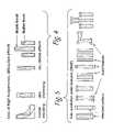
- the challenge in patterning at deep sub-wavelength feature sizesstems from the fact that image patterns as printed on the wafer get distorted from the original intended patterns, as illustrated in FIG. 4 .
- An example of such image shape distortionsis line shortening, whereby the length of a printed line is less than its intended nominal length.
- Another form of image distortionis corner rounding, where an intended sharp corner turns into a rounded one.
- Yet another type of image distortionis the so-called iso-dense effect, whereby lines print thinner when they are isolated (i.e., by themselves) than if they were amidst other patterns.
- the part of a line emerging from a cluster of patternsoften prints thinner than other parts of the same line within the cluster of patterns.
- Other factors that cause the same nominal line width to print differentlyinclude environmental variations, developer induced effects, and etch effects.
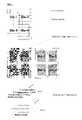
- RET'sespecially OPC techniques, attempt to compensate for patterning process aberrations and variabilities to achieve better patterning accuracy and CD uniformity control.
- Some of these prior art techniquesare illustrated in FIG. 5 .
- OPCoptical proximity corrections
- the simplest OPC examplesattempt to offset the loss of high frequencies or counter the effects of diffraction and/or scattering by appending the intended layout features with sub-resolution assist features or SRAF's such as serifs, hammerheads, corner cutouts, and scattering bars.
- SRAF'sdo not actually print on the wafer, but generate the appropriate optical behavior that results in the intended features to print right.
- MOPCmodel-based OPC
- ROIrule-based OPC
- CD variations todayremain intolerably high, both within an IC chip and across a stepper field, and will become increasingly more problematic at 0.13 ⁇ m and finer feature sizes.
- CD variationsare broadly categorized as across the chip line-width variabilities (ACLV) and across the reticle field line-width variabilities (AFLV).
- ACLVchip line-width variabilities
- AFLVreticle field line-width variabilities
- OPC correctionsmay it be for the 180 and 130 nm generations or prior generations or more state-of-the-art 90 and sub-90 nm generations, OPC and RET implementation is a very time-consuming process, and IC manufacturers are looking for more effective and efficient solutions.
- the present inventionprovides a system and method of modifying the mask layout shapes of an integrated circuit layout design to compensate for reticle field location-specific systematic CD variations resulting from mask writing process variations, lens imperfections in lithographic patterning, and photoresist process variations, as illustrated in FIG. 7 .
- Called PLCProcess-optimized Layout Compensation
- each set of compensation rules according to the present inventionis specifically tailored for a particular mask-writer-patterning-tools-and-resist-process combination, and are performed on a reticle-wide basis.
- the PLC systemconsists of two major components: a tools/resist-process-specific part (the “characterization” phase), which is conducted for each individual specific mask-writer-patterning-tool-and-etch-step or a combination of steps, to generate a unique set of correction strategies, models and rules; and a design/device-specific part (the “applications” phase), which is performed for each integrated circuit device, leading to a PLC mask that optimally corrects the specific process and tool aberrations to produce superior patterns on the wafer.
- the PLC correctionscan be applied in a number of ways, either before, during, after, or instead of, prior art RET applications.
- FIG. 12illustrates a typical example of how PLC is applied at the level of individual layout shapes.
- FIG. 13shows a PLC mask can be optimized for use on multiple steppers.
- a business processfor offering a turnkey service to semiconductor manufacturers to carry out compensation of lithography mask data for imperfections in the patterning process and to carry out other RET methodologies.
- the provider of such turnkey servicepreferably owns and takes total responsibility for implementing the layout compensation task and provides customers with data for manufacturing masks that will lead to further efficiencies and superior patterning accuracy and fidelity.
- FIG. 1is a schematic view of the optical lithography process.
- FIG. 2illustrates the step-and-repeat or step-and-scan transfer of an image on reticle onto a wafer.
- FIG. 3shows a chip design-to-production process flow employing prior art RET techniques.
- FIG. 4shows various types of image distortions.
- FIG. 5illustrates some prior art image distortion correction techniques.
- FIG. 7illustrates the reticle-wide corrections according to the present invention.
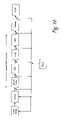
- FIG. 8shows the overall process flow of the present invention.
- FIG. 9shows the various ways of applying the present invention in the RET flow.
- FIG. 10shows the chip design-to-production process flow employing prior art RET and PLC.
- FIG. 11shows some illustrative examples of the concept shown in FIG. 10 .
- FIG. 12shows the flow of a PLC application process.
- FIG. 13shows a PLC mask may be optimized for use with multiple steppers.
- FIG. 14shows a typical flow chart for data flow for implementing OPC and patterning process corrections and components for a turnkey business process.
- FIG. 15illustrates the various steps and operations that can be used to provide customers with a total turnkey solution.
- FIG. 16is an example of maximizing efficiency using shared resources typical of outsourcing.
- FIG. 7there is shown the level of layout compensations as provided by the present invention.
- a set of correction zonesis first mapped onto the field.
- the correction zonesfollow the natural tool/process-induced regions of aberrations.
- these complex aberration regionsmay be reduced to a set of regions with more regular geometrical shapes, such as a grid of rectangular partitions of the same or varying sizes that are sufficiently small that within each such grid, the properties of the aberrations may be described in simpler mathematical terms.
- Each such partitioned spaceis called a Compensation Zone, where a zone is intended as the unit of application of the corrections.
- a rectangular grid of compensation zonesis assumed.
- zoningallows the peculiar local variability characteristics of a particular patterning system to be more fully exploited in the compensation process. All layout shapes that fall within a zone are to be corrected according to one common set of compensation rules, and such rule sets may vary from one zone to another.
- the master image of the layoutwill be arrayed (after applying the appropriate compensations) onto the reticle field.
- the number of such arrayed image copiesmay range from a handful to possibly tens or more.
- one copy of the master layout imagemay end up straddling multiple compensation zones. In that case, two otherwise nominally identical layout shapes may need to be compensated differently if they fall into different zones.
- different copies of the master image, as they are arrayed on top of multiple compensation zoneswill be compensated differently to more fully account for the local, location-specific variabilities.
- the main task of the characterization partis to extract a systematic variability signature that is unique to a tools/photoresist-process combination that may be used to pattern a critical layer during the manufacture of an integrated circuit.
- a set of specifically designed test reticlesis first used with the particular tools and resist process to pattern a number of test wafers.
- Each test reticlecontains a large collection of layout shapes of varying characteristics (different orientations, sizes, densities, . . . ), designed and configured in such a way that the unique variability signature of the tools/resist-process combination will manifest itself in the patterns as printed on the resulting wafers.
- test reticlesincorporate collections of test features designed specifically for each wafer fabrication facility (“fab”) and its design rules to allow for the extraction of the systematic variability signature of a particular patterning process.
- fabwafer fabrication facility
- These characterization reticlesare used to pattern a number of test wafers, using the target stepper and employing a range of process parameters that are likely to be used at the subject fab for the target development and etch processes.
- the wafersthen undergo certain metrology measurements, resulting in a database of as-designed and as-printed feature sizes for various layout shape and pattern types. These measurements will be made within the reticle field of all the wafers, in multiple fields, within a wafer across all the wafers, and within multiple wafers to capture “wafer-to-wafer and lot-to-lot” variabilities.
- the datais then analyzed to both statistically and physically decompose the patterning variability into systematic components and random components.
- the random componentsare stochastic in nature and are best addressed through statistical process control techniques.
- the systematic componentsare unique to the particular tools/resist-process combination, are relatively stable, and are correctable through mask layout compensation.
- the systematic CD componentbasically embodies the unique variability signature of the particular patterning process, from which a set of compensation rules is derived.
- the end result of the data analysesis a unique variability signature of the particular tools/resist-process combination. From the signature, a set of PLC compensation strategies, models and rules for modifying the IC layout is generated.
- FIG. 10illustrates this in greater detail, beginning with circuit design through MDP prior to physical mask production, and FIG. 11 illustrates some more specific examples of how PLC can be applied.
- the design/layout datais subject to specific treatments to achieve certain desired results.
- the techniques of the present inventionare applied to each critical layer of a chip design, following the process flow shown in FIG. 12 . These techniques may be applied prior to, during, or subsequent to, or instead of, the application of the prior art RET techniques.
- the optimal point of PLC applicationis determined based on individual needs of a particular IC designer or fab.
- the applications phase of the present inventionapplies the corrections to the layout shapes of an IC according to the compensation rules. More particularly, for an individual chip design, there are a number of layers for which precise CD control and high CD uniformity will have a major impact on the chip's speed performance (so-called “binning”) and production yield. These are called the “critical layers” of the particular IC layout design.
- the potential economical ramificationgives an IC manufacturer the incentive not only to process such critical layers using the most advanced mask-making and lithographic tools, but also to run the layout data for these layers through the PLC process.
- the additional PLC processing of a layer's layout datamay come before, during, or after the application of the prior art RET techniques.
- the layout data as modified by the PLC applications processis then used to make the “PLC-masks,” which are used in the patterning of the critical layers of the IC.
- each layout shape contained in the GDS fileis retrieved and modified according to the compensation method of the present invention.
- the outputis a corrected GDS file for the particular job partition.
- the whole jobmay be divided among a collection of processing nodes, to reduce the overall turnaround time.
- the final resultis the layout images for the entire reticle field, which is then used to make a PLC reticle, for use in the patterning of the particular layer.
- the PLC applicationcan also be optimized for operation with multiple steppers. This is accomplished by analyzing the signature of each target stepper and identifying components that are both similar and dissimilar. These are used to generate PLC strategies, models and rules for generating optimized masks that can work well with any of the steppers. The optimizations can be further fine-tuned based on user-specifiable weighting factors for expected usage. Such optimization enables a fab to use any stepper in a fab so that the use of a PLC mask does not restrict usage to only one stepper. Such optimization also makes it possible to get the best possible patterning results with a PLC mask on one stepper, for example, while getting acceptable results on other steppers that may be used as emergency backup systems.
- a method and business practice for a customer to outsource post-layout data modificationsis provided.
- an entity that is run independently of a customer, a fabrication facility, and a mask shopobtains a layout design from the customer.
- the entitymodifies the layout design and returns the modified layout design to the customer, fabrication facility, and/or mask shop.
- the modificationcan be based on process and equipment conditions at the fabrication facility and/or mask shop. Additionally, some or all of the modifications can be independent of the process and equipment conditions at the fabrication facility and/or mask shop. For example, some layers of the layout design can be modified using OPC models that do not require, as input, processing and equipment conditions at the fabrication facility and/or mask shop, while other layers are modified based on such process and equipment conditions.
- the entityinstead of merely returning the modified layout design, the entity makes a mask that incorporates the modified layout design and provides the mask to the customer and/or fabrication facility.
- the schematic flow diagramsshow the various steps in implementing corrections to the IC layout to account for patterning tool and process effects and other RET implementations.
- the whole operationmay be limited to simple OPC such as with sub-resolution assist features or SRAF's such as serifs, hammerheads, corner cutouts, and scattering bars.
- an entity 100receives an IC layout from a customer 105 .
- OPC/RET and patterning process correctionsare implemented 115 to modify the layout and prepare modified mask data 120 .
- the mask making data or the masks themselves 125are then provided to the customer, a fabrication facility, and/or a mask shop.
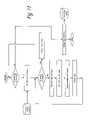
- FIG. 14also shows the steps to determine the patterning process corrections. First, test masks 130 are prepared, and wafers 135 are fabricated. The wafer undergoes wafer metrology 140 , and the resulting data is analyzed 145 to produce a patterning process and proximity correction model and/or OPC/RET rules 150 .
- FIG. 15is a more detailed step-by-step explanation of the entire turkey service process.
- the entityreceives a customer order (act 200 ).
- the entityreceives the customer layout at an on-site location or a central processing location (act 210 ) and carries out any pre-processing operations (act 220 ).
- the entityapplies a layout correction algorithm on each layer (act 230 ).
- the layout correction algorithmpreferably is based on process and equipment conditions at a fabrication facility and/or mask shop.
- the entityidentifies details of the customer IC layout and identifies which mask house will make the mask and which wafer fabrication facility will pattern the mask (act 240 ).
- the entityselects the appropriate test masks to characterize the patterning process (act 250 ).
- the entitythen carries out the patterning process, characterizes the tools used, performs the appropriate mask and wafer metrology, and collects the resulting data (act 260 ). From this data, the entity builds OPC/RET rules or a model to account for patterning process/tool effects (act 270 ).
- the entityAfter the entity applies the layout correction algorithm on each layer (act 230 ), the entity implements post-correction verification though simulation (act 280 ). If necessary, the entity can carry out mask data preparation and fracturing for data to be sent directly for mask making (act 290 ). The entity 100 then transfers data or the mask to the customer (act 300 ).
- the first element of this processis quantitative characterization of the patterning tools and process. Characterization is preferably done at the wafer fab by printing a multitude of test patterns and measuring features of the patterns formed on the wafers. The next step is preferably either generating rules or fitting a model to these observations. Once this is completed, the rules or model can then be applied to the layout.
- the IC layoutis typically in a GDS II or Oasis or equivalent format.
- design rule check (DRC) operationsas well as layer polygon operations including but not limited to Boolean and pre-biasing operations can be performed. Patterning process/tool and proximity corrections are then applied to the layout.
- post-correction verification of the layout and mask data preparationare completed. At this point, the data can be transferred to the customer for mask making or, as part of the turnkey service, a mask set can be made for the customer specific to its design and wafer fab.
- This flowcan also address other operations such as phase shifting masks (PSM) as well as tiling operations to compensate for chemical mechanical polishing effects on the wafer.
- PSMphase shifting masks
- tiling operationsto compensate for chemical mechanical polishing effects on the wafer.
- PSMphase shifting masks
- tiling operationsto compensate for chemical mechanical polishing effects on the wafer.
- a set of resourcesincluding computers, software tools including in-house developed or commercially-available OPC and RET software, networking and data communications bandwidth, physical facilities, wafer test and metrology equipment, and people, including technical experts, operators, and administrative support personnel are preferably used to carry out the turnkey solution.
- Wafer fab characterizationpreferably involves having manpower onsite who will be responsible for collecting data and processing it on-site or sending the data to a central location for processing. Based on the characterization model created, IC layout modifications can be done at a central location or at a customer site using optimized computer system configuration and layout optimization software.
- the integrated turnkey solutionincludes service and support that can be offered on an on-going basis for various design layouts and the manufacturing process used by the manufacturers of ICs.
- the business processcan comprise a set of shared resources consisting of computers, software tools including commercially-available reticle enhancement (RET) software, networking and data communications bandwidth, physical facilities, wafer test and metrology equipment, and people, including technical experts, operators, and administrative support personnel, that can be optimized for any given customer who has a plurality of operations, or, shared amongst a plurality of customers resulting in operational efficiencies.
- RETreticle enhancement
- This business process where a plurality of customers shares common resources to achieve operational efficienciesis akin to outsourcing. This is elaborated in FIG. 16 . As shown in FIG.
- an outsourced turnkey provider 310receives IC layout data files from a plurality of customers (Customers A-N) and information regarding process and equipment conditions from a plurality of wafer fabrication facilities (Wafer Fab A-N).
- Customer A-NIC layout data files
- Wafer Fab A-Nwafer fabrication facilities
- the business modelmay further include any combination of the following: on-site support at a customer site for periodic characterization of customer patterning process; completing all characterization measurements on wafers at common location/locations using standardized metrology tools of known precision and accuracies; electronically or otherwise transferring such characterization information from a single or multiple locations to common location/locations for extraction of tool signature and generating compensation rules or models; electronically or otherwise obtaining customer/customers IC layout design for each layer to common location/locations; modifying the geometric shapes of the layout using the set of compensation rules, to obtain a corrected layout using common multi-tasking computer farm/farms; and electronically or otherwise transferring modified IC layout design back to customer/customers designated location/locations.
- a system for reducing CD variability in lithographic patterning in the manufacture of an integrated circuitmay comprise the steps of characterizing a system and/or process, generating compensation rules, correcting according to such rules, making a compensated reticle/photomask using the corrected layout data, and using the compensated reticle to pattern an IC.
- the characterization stepinvolves characterizing a specific mask writing system, optical projection system, photoresist process, and etch process to obtain a unique variability signature pertaining to that particular tools/patterning-process combination.
- the generating compensation rules stepinvolves generating a set of PLC compensation rules from the unique variability signature.
- the correcting stepinvolves applying reticle field-wide PLC corrections, for any target layer of said IC layout design, by modifying the geometric shapes of the mask layout according to the set of compensation rules, to obtain corrected layout data for the entire reticle.
- the PLC reticle/photomaskis made on the specific mask writing system using the corrected layout data.
- the PLC reticleis used to pattern the particular target layer in the manufacture of the integrated circuit.
- the system described abovemay also comprise generating characterizing reticles, patterning test wafers, taking measurements to create a database, analyzing the database, and generating compensation rules.
- the generating stepcomprises generating a plurality of characterizing reticles containing a plurality of layout features for the purpose of capturing the unique variability signature of a specific patterning process using a specific mask writing tools/optical tools/resist process combination.
- the patterning stepcomprises patterning a plurality of test wafers using the characterizing reticles, through the specific pattering process.
- the measurement stepinvolves performing metrology measurements of the CD's on both the characterizing reticles, the developed wafers, and the etched wafers, to generate a database of variability map data.
- the analyzing stepinvolves analyzing the variability map database to generate the unique variability signature of the specific patterning process. A set of PLC rules are generated for the specific patterning process based on the unique variability signature.
- the characterizing reticlesmay contain: appropriate design to represent the actual device layout and fab design rules vis-à-vis appropriate CDs, pitches, densities as well as isolated and dense patterns and pattern directions; appropriate probing structures for electrical line width measurements; and appropriate structures for measurements by CD-SEM (scanning electron microscope), optical scatterometry and cross-section SEM and TEM.
- the metrology measurements processcan also include the steps of: measuring CD's on the characterizing reticles using CD-SEM or scatterometry to generate a portion of the data for the variability map database; measuring CD's on the developed test wafers using CD-SEM to generate yet another portion of the data for the variability map database; performing electrical linewidth measurements (ELM) on the etched test wafers to generate further data for the variability map database; and performing measurements on pre-calibrated metrology tools that have used standardized calibration wafer sets.
- ELMelectrical linewidth measurements
- the variability map database analysis processcan also include the steps of: organizing the database appropriately for extraction of statistical (stochastic) components and deterministic (signature) components; performing statistical decomposition to extract the systematic/deterministic signature from the variability data using Discrete Fourier Transforms; performing physical/causal decomposition of the deterministic signature through formulation of a collection of linear regression fitted transfer functions of the patterning tools.
- the derivation of PLC compensation rulescan also include steps directed to generating correction zones and generating compensation rules for each such zone.
- generating the correction zonescan involve generating an optimal number of correction zones such that (a) the correction zones are defined by regular geometric areas, such as rectangles, that facilitate selection of a cluster of layout patterns that fall within the correction zones; (b) the number of correction zones are a function of the degree of intra-field variabilities as well as the desired level of corrections; and (c) within each such correction zone, the variabilities can be sufficiently simplified and mathematically represented in a manner that facilitates the generation of one set of compensation rules that can be applied in practice with great computational efficiencies.
- Generating compensation rulescan involve, for each correction zone, a function of the feature size, pitch, density, orientation (vertical or horizontal); stepper settings such as focus, exposure dose, partial coherence and numerical aperture; and certain other process parameters in the resist and post-resist bake processes.
- the process of applying PLC corrections to a particular target layer of the IC layoutcan also include partitioning. Specifically, the process can include reading in the reticle layout information and creating one job partition for each instance of the master layout image to be mapped onto the reticle field. Then, for each job partition, reading in the GDS layout data file of the target layer and applying the corrections to the layout data according to the PLC rules.
- This input layout in GDS, or another formatcan be the output of a prior art RET process.
- the PLCcan be applied prior to, during, subsequent to, or instead of a prior art RET process.
- the application of PLCcan be performed in a multiprocessing setting, either in a distributed configuration among a plurality of processor nodes connected through a network, or among multiple processors assembled within one node.
- the integrated turnkey solutionincludes service and support for characterizing a specific projection optical system and photoresist process to obtain a unique variability signature pertaining to that particular tools/resist-process combination. This is offered on an on-going basis for all the patterning tools used by the manufacturers of integrated circuit.
- the business practiceincludes providing service and support to obtain a unique variability signature pertaining to that particular tools/resist-process combination based on the data obtained. It also includes providing service and support for deriving a set of compensation rules from the unique variability signature.
- the businessincludes service and support for each target layer of an IC layout design, including modifying the geometric shapes of the layout using the set of compensation rules to obtain a corrected layout. It also includes service and support for making a reticle/photomask using the corrected layout data, and for using the corrected reticle to pattern the particular target layer in the manufacture of the integrated circuit.
- the businesswould comprise a set of shared resources consisting of computers, software tools, networking and data communications bandwidth, physical facilities, wafer test and metrology equipment, and people, including technical experts, operators, and administrative support personnel, that can be shared amongst a plurality of customers, resulting in operational efficiencies to provide the above-described services.
- the business modelmay further include any combination of the following: on-site support at customer site for periodic characterization of customer patterning process; completing all characterization measurements on wafers at common location/locations using standardized metrology tools of known precision and accuracies; electronically or otherwise transferring such characterization information from a single or multiple locations to common location/locations for extraction of tool signature and generating compensation rules; electronically or otherwise obtaining customer/customers IC layout design for each layer to common location/locations; modifying the geometric shapes of the layout using the set of compensation rules, to obtain a corrected layout using common multi-tasking computer farm/farms; electronically or otherwise transferring modified IC layout design back to customer/customers designated location/locations.
- the PLC compensation rules generatedcan optionally be optimized for providing user-desired performance across a plurality of steppers based on user-definable weighting factors.
- a method of practicing the Resolution Enhancement Technology (RET), through mask layout corrections on an entire-reticle-field-wide basis, in lithographic patterning in the manufacture of integrated circuitscan include characterizing a system, deriving and applying compensation rules, making a corrected reticle, and patterning.
- a specific patterning systemis characterized, in its entirety, including the specific tools used and the process steps performed, to derive a unique variability signature of the specific system. Then, a plurality of compensation rules sets are derived from the unique variability signature. For each mask layout layer of an IC for which the application of RET is desired, corrections are performed, using the sets of compensation rules to generate a corrected layout data file(s) for the entire reticle field. Then, a corrected reticle is made using the corrected reticle field wide layout data. The corrected reticle is used to pattern the particular layer of the IC.
- RETResolution Enhancement Technology
- the rules setscan be constructed substantially in the form of multi-dimensional look-up tables of compensation factors for fast retrieval and expeditious execution, specifically without resorting to such time-consuming techniques as real-time optical or process simulations.
- rules look-up tablescan be keyed substantially by, but not limited to, such attributes of the layout shapes as the location in the reticle field, the size, orientation, and pattern density, and such tool settings and process parameters as the exposure dosage, the focus, and etch process parameter settings.
- the original reticlemay consist of a plurality of layouts that are not for exactly the same device, and PLC corrections are applied to these multiple devices on a reticle location-specific basis.
Landscapes
- Physics & Mathematics (AREA)
- General Physics & Mathematics (AREA)
- Exposure And Positioning Against Photoresist Photosensitive Materials (AREA)
- Preparing Plates And Mask In Photomechanical Process (AREA)
Abstract
Description
CD=k1(λ/NA)
where λ is the wavelength of the exposure light, NA is the numerical aperture of the projection system, and k1is a process-related factor that serves as a measure of the degree of “difficulty” of the lithographic process.
Claims (36)
Priority Applications (1)
| Application Number | Priority Date | Filing Date | Title |
|---|---|---|---|
| US10/841,079US7318214B1 (en) | 2003-06-19 | 2004-05-07 | System and method for reducing patterning variability in integrated circuit manufacturing through mask layout corrections |
Applications Claiming Priority (2)
| Application Number | Priority Date | Filing Date | Title |
|---|---|---|---|
| US48028603P | 2003-06-19 | 2003-06-19 | |
| US10/841,079US7318214B1 (en) | 2003-06-19 | 2004-05-07 | System and method for reducing patterning variability in integrated circuit manufacturing through mask layout corrections |
Publications (1)
| Publication Number | Publication Date |
|---|---|
| US7318214B1true US7318214B1 (en) | 2008-01-08 |
Family
ID=38893487
Family Applications (1)
| Application Number | Title | Priority Date | Filing Date |
|---|---|---|---|
| US10/841,079Expired - LifetimeUS7318214B1 (en) | 2003-06-19 | 2004-05-07 | System and method for reducing patterning variability in integrated circuit manufacturing through mask layout corrections |
Country Status (1)
| Country | Link |
|---|---|
| US (1) | US7318214B1 (en) |
Cited By (93)
| Publication number | Priority date | Publication date | Assignee | Title |
|---|---|---|---|---|
| US20060288325A1 (en)* | 2005-06-15 | 2006-12-21 | Atsushi Miyamoto | Method and apparatus for measuring dimension of a pattern formed on a semiconductor wafer |
| US20070026322A1 (en)* | 2005-08-01 | 2007-02-01 | Chin-Cheng Yang | Integration system and the method for operating the same |
| US20070264584A1 (en)* | 2006-02-13 | 2007-11-15 | Samsung Electronics Co., Ltd. | Pattern arrangement method of semiconductor device |
| US20080148194A1 (en)* | 2006-12-18 | 2008-06-19 | Cadence Design Systems, Inc. | Method and system for process optimization |
| US20080148216A1 (en)* | 2006-12-18 | 2008-06-19 | Cadence Design Systems, Inc. | Method and system for mask optimization |
| US20080147374A1 (en)* | 2006-12-18 | 2008-06-19 | Cadence Design Systems, Inc. | Modeling and cross correlation of design predicted criticalities for optimization of semiconductor manufacturing |
| US20080148195A1 (en)* | 2006-12-18 | 2008-06-19 | Cadence Design Systems, Inc. | Method and system for inspection optimization |
| US7409656B1 (en) | 2005-09-12 | 2008-08-05 | Cadence Design Systems, Inc. | Method and system for parallelizing computing operations |
| US20080241709A1 (en)* | 2007-04-02 | 2008-10-02 | Kent Nakagawa | System And Method For analyzing photomask Geometries |
| US20080263501A1 (en)* | 2007-04-23 | 2008-10-23 | Taiwan Semiconductor Manufacturing Company, Ltd. | System, Method, and Computer-Readable Medium for Performing Data Preparation for a Mask Design |
| US20090100386A1 (en)* | 2006-06-19 | 2009-04-16 | International Business Machines Corporation | IC Layout Optimization to Improve Yield |
| US7653892B1 (en) | 2004-08-18 | 2010-01-26 | Cadence Design Systems, Inc. | System and method for implementing image-based design rules |
| US7657856B1 (en)* | 2006-09-12 | 2010-02-02 | Cadence Design Systems, Inc. | Method and system for parallel processing of IC design layouts |
| US20100209830A1 (en)* | 2009-02-13 | 2010-08-19 | Tokyo Electron Limited | Multi-Pitch Scatterometry Targets |
| US20100218159A1 (en)* | 2008-11-19 | 2010-08-26 | Emile Sahouria | Data Flow Branching in Mask Data Preparation |
| US20100333049A1 (en)* | 2009-06-26 | 2010-12-30 | International Business Machines Corporation | Model-Based Retargeting of Layout Patterns for Sub-Wavelength Photolithography |
| US7904852B1 (en) | 2005-09-12 | 2011-03-08 | Cadence Design Systems, Inc. | Method and system for implementing parallel processing of electronic design automation tools |
| US7913206B1 (en) | 2004-09-16 | 2011-03-22 | Cadence Design Systems, Inc. | Method and mechanism for performing partitioning of DRC operations |
| US20110138342A1 (en)* | 2009-12-03 | 2011-06-09 | International Business Machines Corporation | Retargeting for Electrical Yield Enhancement |
| US20110161907A1 (en)* | 2009-12-28 | 2011-06-30 | Taiwan Semiconductor Manufacturing Company, Ltd. | Practical Approach to Layout Migration |
| WO2012003511A1 (en)* | 2010-07-02 | 2012-01-05 | Tfri, Inc. | Fabrication process for embedded passive components |
| US8146026B2 (en) | 2009-11-17 | 2012-03-27 | International Business Machines Corporation | Simultaneous photolithographic mask and target optimization |
| US8331646B2 (en) | 2009-12-23 | 2012-12-11 | International Business Machines Corporation | Optical proximity correction for transistors using harmonic mean of gate length |
| US8381152B2 (en) | 2008-06-05 | 2013-02-19 | Cadence Design Systems, Inc. | Method and system for model-based design and layout of an integrated circuit |
| US8448096B1 (en) | 2006-06-30 | 2013-05-21 | Cadence Design Systems, Inc. | Method and system for parallel processing of IC design layouts |
| US8499260B2 (en) | 2011-01-26 | 2013-07-30 | International Business Machines Corporation | Optical proximity correction verification accounting for mask deviations |
| US8555210B2 (en) | 2011-04-29 | 2013-10-08 | Micron Technology, Inc. | Systems and methods for stochastic models of mask process variability |
| US8577489B2 (en) | 2011-01-26 | 2013-11-05 | International Business Machines Corporation | Diagnosing in-line critical dimension control adjustments using optical proximity correction verification |
| US8578303B1 (en) | 2012-07-06 | 2013-11-05 | National Taiwan University | Method for compensating effect of patterning process and apparatus thereof |
| US8601423B1 (en)* | 2012-10-23 | 2013-12-03 | Netspeed Systems | Asymmetric mesh NoC topologies |
| US8619236B2 (en) | 2010-11-24 | 2013-12-31 | International Business Machines Corporation | Determining lithographic set point using optical proximity correction verification simulation |
| US8885510B2 (en) | 2012-10-09 | 2014-11-11 | Netspeed Systems | Heterogeneous channel capacities in an interconnect |
| US8934377B2 (en) | 2013-03-11 | 2015-01-13 | Netspeed Systems | Reconfigurable NoC for customizing traffic and optimizing performance after NoC synthesis |
| US9007920B2 (en) | 2013-01-18 | 2015-04-14 | Netspeed Systems | QoS in heterogeneous NoC by assigning weights to NoC node channels and using weighted arbitration at NoC nodes |
| US9009648B2 (en) | 2013-01-18 | 2015-04-14 | Netspeed Systems | Automatic deadlock detection and avoidance in a system interconnect by capturing internal dependencies of IP cores using high level specification |
| US9054977B2 (en) | 2013-08-05 | 2015-06-09 | Netspeed Systems | Automatic NoC topology generation |
| US20150213161A1 (en)* | 2014-01-30 | 2015-07-30 | International Business Machines Corporation | Optical model employing phase transmission values for sub-resolution assist features |
| US9130856B2 (en) | 2013-01-28 | 2015-09-08 | Netspeed Systems | Creating multiple NoC layers for isolation or avoiding NoC traffic congestion |
| US9160627B2 (en) | 2013-04-04 | 2015-10-13 | Netspeed Systems | Multiple heterogeneous NoC layers |
| US9158882B2 (en) | 2013-12-19 | 2015-10-13 | Netspeed Systems | Automatic pipelining of NoC channels to meet timing and/or performance |
| US9185026B2 (en) | 2012-12-21 | 2015-11-10 | Netspeed Systems | Tagging and synchronization for fairness in NOC interconnects |
| US9185023B2 (en) | 2013-05-03 | 2015-11-10 | Netspeed Systems | Heterogeneous SoC IP core placement in an interconnect to optimize latency and interconnect performance |
| US9223711B2 (en) | 2013-08-13 | 2015-12-29 | Netspeed Systems | Combining associativity and cuckoo hashing |
| US9244880B2 (en) | 2012-08-30 | 2016-01-26 | Netspeed Systems | Automatic construction of deadlock free interconnects |
| US9244845B2 (en) | 2014-05-12 | 2016-01-26 | Netspeed Systems | System and method for improving snoop performance |
| US9253085B2 (en) | 2012-12-21 | 2016-02-02 | Netspeed Systems | Hierarchical asymmetric mesh with virtual routers |
| US9294354B2 (en) | 2013-10-24 | 2016-03-22 | Netspeed Systems | Using multiple traffic profiles to design a network on chip |
| US9319232B2 (en) | 2014-04-04 | 2016-04-19 | Netspeed Systems | Integrated NoC for performing data communication and NoC functions |
| US9444702B1 (en) | 2015-02-06 | 2016-09-13 | Netspeed Systems | System and method for visualization of NoC performance based on simulation output |
| US9473388B2 (en) | 2013-08-07 | 2016-10-18 | Netspeed Systems | Supporting multicast in NOC interconnect |
| US9473359B2 (en) | 2014-06-06 | 2016-10-18 | Netspeed Systems | Transactional traffic specification for network-on-chip design |
| US9471726B2 (en) | 2013-07-25 | 2016-10-18 | Netspeed Systems | System level simulation in network on chip architecture |
| US9473415B2 (en) | 2014-02-20 | 2016-10-18 | Netspeed Systems | QoS in a system with end-to-end flow control and QoS aware buffer allocation |
| US9477280B1 (en) | 2014-09-24 | 2016-10-25 | Netspeed Systems | Specification for automatic power management of network-on-chip and system-on-chip |
| US9519732B1 (en) | 2011-11-28 | 2016-12-13 | Cadence Design Systems, Inc. | Methods, systems, and articles of manufacture for implementing pattern-based design enabled manufacturing of electronic circuit designs |
| US9529400B1 (en) | 2014-10-29 | 2016-12-27 | Netspeed Systems | Automatic power domain and voltage domain assignment to system-on-chip agents and network-on-chip elements |
| US9535848B2 (en) | 2014-06-18 | 2017-01-03 | Netspeed Systems | Using cuckoo movement for improved cache coherency |
| US9568970B1 (en) | 2015-02-12 | 2017-02-14 | Netspeed Systems, Inc. | Hardware and software enabled implementation of power profile management instructions in system on chip |
| US9571402B2 (en) | 2013-05-03 | 2017-02-14 | Netspeed Systems | Congestion control and QoS in NoC by regulating the injection traffic |
| US9571341B1 (en) | 2014-10-01 | 2017-02-14 | Netspeed Systems | Clock gating for system-on-chip elements |
| US9660942B2 (en) | 2015-02-03 | 2017-05-23 | Netspeed Systems | Automatic buffer sizing for optimal network-on-chip design |
| US9699079B2 (en) | 2013-12-30 | 2017-07-04 | Netspeed Systems | Streaming bridge design with host interfaces and network on chip (NoC) layers |
| US9742630B2 (en) | 2014-09-22 | 2017-08-22 | Netspeed Systems | Configurable router for a network on chip (NoC) |
| US9762474B2 (en) | 2014-04-07 | 2017-09-12 | Netspeed Systems | Systems and methods for selecting a router to connect a bridge in the network on chip (NoC) |
| US9774498B2 (en) | 2012-12-21 | 2017-09-26 | Netspeed Systems | Hierarchical asymmetric mesh with virtual routers |
| US9781043B2 (en) | 2013-07-15 | 2017-10-03 | Netspeed Systems | Identification of internal dependencies within system components for evaluating potential protocol level deadlocks |
| US9825809B2 (en) | 2015-05-29 | 2017-11-21 | Netspeed Systems | Dynamically configuring store-and-forward channels and cut-through channels in a network-on-chip |
| US9830265B2 (en) | 2013-11-20 | 2017-11-28 | Netspeed Systems, Inc. | Reuse of directory entries for holding state information through use of multiple formats |
| US9864728B2 (en) | 2015-05-29 | 2018-01-09 | Netspeed Systems, Inc. | Automatic generation of physically aware aggregation/distribution networks |
| US9928204B2 (en) | 2015-02-12 | 2018-03-27 | Netspeed Systems, Inc. | Transaction expansion for NoC simulation and NoC design |
| US10027433B2 (en) | 2013-06-19 | 2018-07-17 | Netspeed Systems | Multiple clock domains in NoC |
| US10042404B2 (en) | 2014-09-26 | 2018-08-07 | Netspeed Systems | Automatic generation of power management sequence in a SoC or NoC |
| US10050843B2 (en) | 2015-02-18 | 2018-08-14 | Netspeed Systems | Generation of network-on-chip layout based on user specified topological constraints |
| US10063496B2 (en) | 2017-01-10 | 2018-08-28 | Netspeed Systems Inc. | Buffer sizing of a NoC through machine learning |
| US10084725B2 (en) | 2017-01-11 | 2018-09-25 | Netspeed Systems, Inc. | Extracting features from a NoC for machine learning construction |
| US10218580B2 (en) | 2015-06-18 | 2019-02-26 | Netspeed Systems | Generating physically aware network-on-chip design from a physical system-on-chip specification |
| US10298485B2 (en) | 2017-02-06 | 2019-05-21 | Netspeed Systems, Inc. | Systems and methods for NoC construction |
| US10313269B2 (en) | 2016-12-26 | 2019-06-04 | Netspeed Systems, Inc. | System and method for network on chip construction through machine learning |
| US20190179996A1 (en)* | 2017-12-12 | 2019-06-13 | Mentor Graphics Corporation | Puzzle-based pattern analysis and classification |
| US10348563B2 (en) | 2015-02-18 | 2019-07-09 | Netspeed Systems, Inc. | System-on-chip (SoC) optimization through transformation and generation of a network-on-chip (NoC) topology |
| US10419300B2 (en) | 2017-02-01 | 2019-09-17 | Netspeed Systems, Inc. | Cost management against requirements for the generation of a NoC |
| US10452124B2 (en) | 2016-09-12 | 2019-10-22 | Netspeed Systems, Inc. | Systems and methods for facilitating low power on a network-on-chip |
| US10528682B2 (en) | 2014-09-04 | 2020-01-07 | Netspeed Systems | Automatic performance characterization of a network-on-chip (NOC) interconnect |
| US10547514B2 (en) | 2018-02-22 | 2020-01-28 | Netspeed Systems, Inc. | Automatic crossbar generation and router connections for network-on-chip (NOC) topology generation |
| US10657420B2 (en) | 2018-07-17 | 2020-05-19 | International Business Machines Corporation | Modeling post-lithography stochastic critical dimension variation with multi-task neural networks |
| US10691869B2 (en)* | 2018-02-24 | 2020-06-23 | Mentor Graphics Corporation | Pattern-based optical proximity correction |
| US10735335B2 (en) | 2016-12-02 | 2020-08-04 | Netspeed Systems, Inc. | Interface virtualization and fast path for network on chip |
| US10860762B2 (en) | 2019-07-11 | 2020-12-08 | Intel Corpration | Subsystem-based SoC integration |
| US10896476B2 (en) | 2018-02-22 | 2021-01-19 | Netspeed Systems, Inc. | Repository of integration description of hardware intellectual property for NoC construction and SoC integration |
| US10983910B2 (en) | 2018-02-22 | 2021-04-20 | Netspeed Systems, Inc. | Bandwidth weighting mechanism based network-on-chip (NoC) configuration |
| US11023377B2 (en) | 2018-02-23 | 2021-06-01 | Netspeed Systems, Inc. | Application mapping on hardened network-on-chip (NoC) of field-programmable gate array (FPGA) |
| US11144457B2 (en) | 2018-02-22 | 2021-10-12 | Netspeed Systems, Inc. | Enhanced page locality in network-on-chip (NoC) architectures |
| US11176302B2 (en) | 2018-02-23 | 2021-11-16 | Netspeed Systems, Inc. | System on chip (SoC) builder |
Citations (38)
| Publication number | Priority date | Publication date | Assignee | Title |
|---|---|---|---|---|
| US5308991A (en) | 1992-06-02 | 1994-05-03 | National Semiconductor Corporation | Method and apparatus for making a predistorted reticle to compensate for lens distortions |
| US5528508A (en) | 1993-02-19 | 1996-06-18 | International Business Machines Corporation | System and method for verifying a hierarchical circuit design |
| US5573890A (en) | 1994-07-18 | 1996-11-12 | Advanced Micro Devices, Inc. | Method of optical lithography using phase shift masking |
| US5705301A (en) | 1996-02-27 | 1998-01-06 | Lsi Logic Corporation | Performing optical proximity correction with the aid of design rule checkers |
| US5858580A (en) | 1997-09-17 | 1999-01-12 | Numerical Technologies, Inc. | Phase shifting circuit manufacture method and apparatus |
| US5862058A (en) | 1996-05-16 | 1999-01-19 | International Business Machines Corporation | Optical proximity correction method and system |
| US5888675A (en) | 1996-12-04 | 1999-03-30 | Advanced Micro Devices, Inc. | Reticle that compensates for radiation-induced lens error in a photolithographic system |
| US5978085A (en) | 1997-03-07 | 1999-11-02 | Litel Instruments | Apparatus method of measurement and method of data analysis for correction of optical system |
| US6048651A (en) | 1998-10-23 | 2000-04-11 | International Business Machines Corporation | Fresnel zone mask for pupilgram |
| US6091486A (en) | 1999-01-05 | 2000-07-18 | International Business Machines Corporation | Blazed grating measurements of lithographic lens aberrations |
| US6130747A (en) | 1998-02-19 | 2000-10-10 | Kabushiki Kaisha Toshiba | Method of measuring aberrations of lens |
| US6269472B1 (en) | 1996-02-27 | 2001-07-31 | Lsi Logic Corporation | Optical proximity correction method and apparatus |
| US6289499B1 (en) | 1997-12-31 | 2001-09-11 | Avant! Corporation | Proximity correction software for wafer lithography |
| US6303251B1 (en) | 1998-07-29 | 2001-10-16 | Matsushita Electric Industrial Co., Ltd. | Mask pattern correction process, photomask and semiconductor integrated circuit device |
| US6311319B1 (en) | 1998-05-22 | 2001-10-30 | Taiwan Semiconductor Manufacturing Company | Solving line-end shortening and corner rounding problems by using a simple checking rule |
| US6356345B1 (en) | 1998-02-11 | 2002-03-12 | Litel Instruments | In-situ source metrology instrument and method of use |
| US6396569B2 (en) | 1999-09-02 | 2002-05-28 | Texas Instruments Incorporated | Image displacement test reticle for measuring aberration characteristics of projection optics |
| US6403477B1 (en) | 1999-10-25 | 2002-06-11 | Nec Corporation | Method for correcting an optical proximity effect in an interconnect pattern by shortening the legs of cutout patterns to avoid linewidth reduction |
| US6413683B1 (en) | 2000-06-23 | 2002-07-02 | International Business Machines Corporation | Method for incorporating sub resolution assist features in a photomask layout |
| US20020091986A1 (en) | 2001-01-11 | 2002-07-11 | International Business Machines Corporation | Process window based optical proximity correction of lithographic images |
| US6430737B1 (en) | 2000-07-10 | 2002-08-06 | Mentor Graphics Corp. | Convergence technique for model-based optical and process correction |
| US6444373B1 (en) | 2000-06-16 | 2002-09-03 | Advanced Micro Devices, Inc. | Modification of mask layout data to improve mask fidelity |
| US6453457B1 (en) | 2000-09-29 | 2002-09-17 | Numerical Technologies, Inc. | Selection of evaluation point locations based on proximity effects model amplitudes for correcting proximity effects in a fabrication layout |
| US6453452B1 (en) | 1997-12-12 | 2002-09-17 | Numerical Technologies, Inc. | Method and apparatus for data hierarchy maintenance in a system for mask description |
| US20020138810A1 (en) | 2001-01-31 | 2002-09-26 | Lavin Mark A. | Optical proximity correction (OPC) using automated shape and edge pre-sorting |
| US6470489B1 (en) | 1997-09-17 | 2002-10-22 | Numerical Technologies, Inc. | Design rule checking system and method |
| GB2375403A (en) | 2001-05-11 | 2002-11-13 | Mitel Semiconductor Ltd | Optical proximity correction |
| US6529623B1 (en) | 1999-08-31 | 2003-03-04 | Advanced Micro Devices, Inc. | Stepper lens specific reticle compensation for critical dimension control |
| US6532585B1 (en) | 1998-03-03 | 2003-03-11 | Lsi Logic Corporation | Method and apparatus for application of proximity correction with relative segmentation |
| US6553559B2 (en) | 2001-01-05 | 2003-04-22 | International Business Machines Corporation | Method to determine optical proximity correction and assist feature rules which account for variations in mask dimensions |
| US20030088847A1 (en) | 2001-11-07 | 2003-05-08 | Numerical Technologies, Inc. | Method of incorporating lens aberration information into various process flows |
| US20030098970A1 (en) | 2000-12-06 | 2003-05-29 | Asml Masktools Netherlands B.V. | Method and apparatus for detecting aberrations in a projection lens utilized for projection optics |
| US6584609B1 (en) | 2000-02-28 | 2003-06-24 | Numerical Technologies, Inc. | Method and apparatus for mixed-mode optical proximity correction |
| US20030121021A1 (en) | 2001-12-26 | 2003-06-26 | Numerical Technologies, Inc. | System and method for determining manufacturing error enhancement factor |
| US20030192025A1 (en) | 2002-04-03 | 2003-10-09 | Numerical Technologies, Inc. | Automated flow in PSM phase assignment |
| US20030192013A1 (en) | 2002-04-05 | 2003-10-09 | Numerical Technologies, Inc. | Method and apparatus for facilitating process-compliant layout optimization |
| US6646729B2 (en) | 2000-02-23 | 2003-11-11 | Asml Netherlands B.V. | Method of measuring aberration in an optical imaging system |
| US6686100B2 (en) | 2000-10-13 | 2004-02-03 | Zarlink Semiconductor Limited | Optical proximity correction method |
- 2004
- 2004-05-07USUS10/841,079patent/US7318214B1/ennot_activeExpired - Lifetime
Patent Citations (39)
| Publication number | Priority date | Publication date | Assignee | Title |
|---|---|---|---|---|
| US5308991A (en) | 1992-06-02 | 1994-05-03 | National Semiconductor Corporation | Method and apparatus for making a predistorted reticle to compensate for lens distortions |
| US5528508A (en) | 1993-02-19 | 1996-06-18 | International Business Machines Corporation | System and method for verifying a hierarchical circuit design |
| US5573890A (en) | 1994-07-18 | 1996-11-12 | Advanced Micro Devices, Inc. | Method of optical lithography using phase shift masking |
| US6269472B1 (en) | 1996-02-27 | 2001-07-31 | Lsi Logic Corporation | Optical proximity correction method and apparatus |
| US5705301A (en) | 1996-02-27 | 1998-01-06 | Lsi Logic Corporation | Performing optical proximity correction with the aid of design rule checkers |
| US5862058A (en) | 1996-05-16 | 1999-01-19 | International Business Machines Corporation | Optical proximity correction method and system |
| US5888675A (en) | 1996-12-04 | 1999-03-30 | Advanced Micro Devices, Inc. | Reticle that compensates for radiation-induced lens error in a photolithographic system |
| US5978085A (en) | 1997-03-07 | 1999-11-02 | Litel Instruments | Apparatus method of measurement and method of data analysis for correction of optical system |
| US5858580A (en) | 1997-09-17 | 1999-01-12 | Numerical Technologies, Inc. | Phase shifting circuit manufacture method and apparatus |
| US6470489B1 (en) | 1997-09-17 | 2002-10-22 | Numerical Technologies, Inc. | Design rule checking system and method |
| US6453452B1 (en) | 1997-12-12 | 2002-09-17 | Numerical Technologies, Inc. | Method and apparatus for data hierarchy maintenance in a system for mask description |
| US6289499B1 (en) | 1997-12-31 | 2001-09-11 | Avant! Corporation | Proximity correction software for wafer lithography |
| US6356345B1 (en) | 1998-02-11 | 2002-03-12 | Litel Instruments | In-situ source metrology instrument and method of use |
| US6130747A (en) | 1998-02-19 | 2000-10-10 | Kabushiki Kaisha Toshiba | Method of measuring aberrations of lens |
| US6532585B1 (en) | 1998-03-03 | 2003-03-11 | Lsi Logic Corporation | Method and apparatus for application of proximity correction with relative segmentation |
| US6311319B1 (en) | 1998-05-22 | 2001-10-30 | Taiwan Semiconductor Manufacturing Company | Solving line-end shortening and corner rounding problems by using a simple checking rule |
| US6303251B1 (en) | 1998-07-29 | 2001-10-16 | Matsushita Electric Industrial Co., Ltd. | Mask pattern correction process, photomask and semiconductor integrated circuit device |
| US6048651A (en) | 1998-10-23 | 2000-04-11 | International Business Machines Corporation | Fresnel zone mask for pupilgram |
| US6091486A (en) | 1999-01-05 | 2000-07-18 | International Business Machines Corporation | Blazed grating measurements of lithographic lens aberrations |
| US6529623B1 (en) | 1999-08-31 | 2003-03-04 | Advanced Micro Devices, Inc. | Stepper lens specific reticle compensation for critical dimension control |
| US6396569B2 (en) | 1999-09-02 | 2002-05-28 | Texas Instruments Incorporated | Image displacement test reticle for measuring aberration characteristics of projection optics |
| US6403477B1 (en) | 1999-10-25 | 2002-06-11 | Nec Corporation | Method for correcting an optical proximity effect in an interconnect pattern by shortening the legs of cutout patterns to avoid linewidth reduction |
| US6646729B2 (en) | 2000-02-23 | 2003-11-11 | Asml Netherlands B.V. | Method of measuring aberration in an optical imaging system |
| US6584609B1 (en) | 2000-02-28 | 2003-06-24 | Numerical Technologies, Inc. | Method and apparatus for mixed-mode optical proximity correction |
| US6444373B1 (en) | 2000-06-16 | 2002-09-03 | Advanced Micro Devices, Inc. | Modification of mask layout data to improve mask fidelity |
| US6413683B1 (en) | 2000-06-23 | 2002-07-02 | International Business Machines Corporation | Method for incorporating sub resolution assist features in a photomask layout |
| US6430737B1 (en) | 2000-07-10 | 2002-08-06 | Mentor Graphics Corp. | Convergence technique for model-based optical and process correction |
| US6453457B1 (en) | 2000-09-29 | 2002-09-17 | Numerical Technologies, Inc. | Selection of evaluation point locations based on proximity effects model amplitudes for correcting proximity effects in a fabrication layout |
| US6686100B2 (en) | 2000-10-13 | 2004-02-03 | Zarlink Semiconductor Limited | Optical proximity correction method |
| US20030098970A1 (en) | 2000-12-06 | 2003-05-29 | Asml Masktools Netherlands B.V. | Method and apparatus for detecting aberrations in a projection lens utilized for projection optics |
| US6553559B2 (en) | 2001-01-05 | 2003-04-22 | International Business Machines Corporation | Method to determine optical proximity correction and assist feature rules which account for variations in mask dimensions |
| US20020091986A1 (en) | 2001-01-11 | 2002-07-11 | International Business Machines Corporation | Process window based optical proximity correction of lithographic images |
| US20020138810A1 (en) | 2001-01-31 | 2002-09-26 | Lavin Mark A. | Optical proximity correction (OPC) using automated shape and edge pre-sorting |
| GB2375403A (en) | 2001-05-11 | 2002-11-13 | Mitel Semiconductor Ltd | Optical proximity correction |
| US20030003385A1 (en) | 2001-05-11 | 2003-01-02 | Brian Martin | Optical proximity correction |
| US20030088847A1 (en) | 2001-11-07 | 2003-05-08 | Numerical Technologies, Inc. | Method of incorporating lens aberration information into various process flows |
| US20030121021A1 (en) | 2001-12-26 | 2003-06-26 | Numerical Technologies, Inc. | System and method for determining manufacturing error enhancement factor |
| US20030192025A1 (en) | 2002-04-03 | 2003-10-09 | Numerical Technologies, Inc. | Automated flow in PSM phase assignment |
| US20030192013A1 (en) | 2002-04-05 | 2003-10-09 | Numerical Technologies, Inc. | Method and apparatus for facilitating process-compliant layout optimization |
Non-Patent Citations (59)
| Title |
|---|
| "Characterizing Flare of a Projection Lens," U.S. Appl. No. 10/933,090, filed Sep. 1, 2004, inventors: Bo Wu, Abdurrahman Sezginer, Franz X. Zach. |
| "Correcting Design Data for Manufacture," U.S. Appl. No. 10/860,852, filed Jun. 4, 2004, inventors: Vishnu Kamat. |
| "Litel Instruments-ISI Product Overview," http://litel.net/isi<SUB>-</SUB>product.htm, 2 pages, printed Jan. 26, 2004. |
| "Method and System for Designing Manufacturable Patterns that Account for the Pattern- and Position-Dependent Nature of Patterning Processes," U.S. Appl. No. 10/861,170, filed Jun. 4, 2004, inventor: Abdurrahman Sezinger. |
| "Method for Characterization of the Illuminator in a Lithographic System," U.S. Appl. No. 10/960,357, filed Oct. 6, 2004, inventors: Franz X. Zach, Bo Wu, and Abdurrahman Sezinger. |
| "Method for Correcting Position-Dependent Distortions," U.S. Appl. No. 10/933,192, filed Aug. 31, 2004, inventors: Devendra Joshi, Abdurrahman Sezginer, Franz X. Zach. |
| "Method of Characterizing Flare," Invarium, Inc. U.S. Appl. No. 10/860,853, filed Jun. 4, 2004, inventors: Bo Wu, Abdurrahman Sezginer. |
| "System and Method for Compensating for Aberrations in a Photolithographic Process," U.S. Appl. No. 10/841,025, filed May 7, 2004, inventor: Roy V. Prasad. |
| "System and Method for Reducing Patterning Variability in Integrated Circuit Manufacturing through Mask Layout Corrections," U.S. Appl. No. 10/841,079, filed May 7, 2004, inventors: Roy V. Prasad, Chi-Song Horng, and Ram S. Ramanujam. |
| "'The MEEF Meter': a Realistic Approach for Lithography Process Monitoring," Yield Management Solutions, pp. 52-57 (Aug. 2000). |
| A. K-T Wong, Resolution enhancement techniques in optical lithography, SPIE Press, vol. TT47, Bellingham, WA, pp. 91-115, 2001. |
| A. Rosenbluth et al., "Fast Calculation of Images for High Numerical Aperture Lithography," Proceedings of the SPIE vol. 5377 (2004), p. 615. |
| Abramowitz, M. and Stegun, I. A. (Eds.), Ch. 22, Handbook of Mathematical Functions with Formulas, Graphs, and Mathematical Tables, 9th printing. New York: Dover, pp. 771-802, 1972. |
| Born and Wolf, "Principles of Optics," Cambridge University Press, 7<SUP>th </SUP>edition, pp. 459-490, 1999. |
| Born, M. and Wolf, E., Principles of Optics, Ch. 9, 6th ed. New York: Pergamon Press, pp. 459-490 and 523-527, 1989. |
| C. Bodendorf, et al., Impact of measured pupil illumination fill distribution on lithography simulation and OPC models, Proc. SPIE vol. 5377, Article 110, 2004. |
| C. Mack, "Inside PROLITH: A Comprehensive Guide to Optical Lithography Simulation," pp. 67-112, 1997, Finle Technologies, Austin, TX. |
| D.G. Flagello, "Theory of high-NA imaging in homogeneous thin films," Optical Society of America, A, vol. 13, No. 1, 1996. |
| Dirksen et al., "Novel Aberration Monitor for Optical Lithography," Proc. SPIE vol. 3679 (1999), p. 77. |
| E. Luce et al., "Flare impact on the intrafield CD control for sub-0.25 um patterning," SPIE vol. 3679, p. 368-381, Mar. 1999. |
| Erdmann et al., "Comparison of Simulation Approaches for Chemically Amplified Resists," SPIE vol. 4404, 12 pages, undated. |
| F. Zach et al. "Aberration Analysis using Reconstructed Aerial images of Isolated Contacts on Attenuated Phase shift masks." |
| F. Zach, "Neural Network Based Approach to Resist Modeling and OPC," Proceedings of the SPIE, vol. 5377 (2004) p. 670. |
| Frank M. Schellenberg, "Resolution Enhancement with OPC/PSM," Future Fab Intl., vol. 9, Jan. 2000. |
| G. McIntyre et al., "Characterizing illumination angular uniformity with phase shifting masks," Proc. SPIE vol. 5040, Article 16, 2003, SPIE Bellingham, WA. |
| Gill, P. R.; Murray, W.; and Wright, M. H. "The Levenberg-Marquardt Method," §4.7.3 in Practical Optimization. London: Academic Press, pp. 136-137, 1981. |
| Golub, G. H. and Van Loan, C. F., Matrix Computations, Sect. 2.5.3 and 2.5.6, 3rd ed. Baltimore, MD: Johns Hopkins University Press, 1996. |
| Granik et al., "New Process Models for OPC at sub-90nm Nodes," Deep Submicron Technical Publications, presented at SPIE 2003, 11 pages, May 2003. |
| Granik, "Dry etch proximity modeling in mask fabrication," Yuri Publication: Proc. SPIE vol. 5130, p. 86-91, Photomask and Next-Generation Lithography Mask Technology X; Hiroyoshi Tanabe; Ed. (Aug. 2003). |
| H. J. Levinson, Principles of Lithography, SPIE Press, Bellingham, WA, pp. 257-283 and 771-802, 2001. |
| H. Nomura et al., "Higher order aberration measurement with printed patterns under extremely reduced 6 illumination," Proc. SPIE vol. 3679, p. 358-367, SPIE, Bellingham, WA, 1999. |
| Haolin Zhang, "Casual Analysis of Systematic Spatial Variation in Optical Lithography," Ph.D. Thesis, Univ. of Calif., Berkeley, 14 pages, Jun. 2002. |
| J. P. Cain, "Characterization of Spatial Variation in Photolithography," M.S. thesis, University of California, Berkeley, 2002. |
| J. P. Kirk et al. "Pupil Illumination; in situ measurement of partial coherence", Proc. SPIE vol. 3334, 1998, p. 281-288. |
| J. Schacht et al., "Calibration of OPC models for multiple focus conditions," Proc. SPIE. vol. 5377 (2004), p. 691-702. |
| J.A. Kong, Electromagnetic Wave Theory, John Wiley & Sons, 2nd Ed., pp. 370-403, 1990. |
| J.M. Geary, Introduction to Wavefront Sensors, vol. TT18, SPIE Optical Engineering Press, Bellingham, WA, pp. 53-103, 1995. |
| J.P. Kirk et al., "Application of blazed gratings for determination of equivalent primary azimuthal aberrations," Proc. SPIE vol. 3679, p. 70-76, 1999. |
| J.P. Kirk, "Scattered light in photolithographic lenses," Proc SPIE 2197, p. 566-572, SPIE, Bellingham, WA, 1994. |
| J.P. Stirniman, M.L. Rieger, "Fast proximity correction with zone sampling," Proc. SPIE, vol. 2197, pp. 294-301, 1994. |
| Jason P. Cain and Costas J. Spanos, "Electrical linewidth metrology for systematic CD variation characterization and causal analysis," Proc. SPIE, vol. 5038, pp. 350-361, 2003. |
| Kirkpatrick, S., C. D. Gelatt Jr., M. P. Vecchi, "Optimization by Simulated Annealing," Science, 220, No. 4598, pp. 671-680, 1983. |
| Koza, J. R., "Genetic Programming: On the Programming of Computers by Means of Natural Selection," Cambridge, MA: MIT Press, 1992. |
| Liebmann, "Layout Impact of Resolution Enhancement Techniques: Impediment or Opportunity?," ISPD '03, Monterey, CA, pp. 110-117, Apr. 2003. |
| M. Terry et al., "Behavior of lens aberrations as a function of wavelength on KrF and ArF lithography scanners," Proc. SPIE vol. 4346, p. 15-24, 2001. |
| Mark van der Kerkof, et al, "Full optical column characterization of DUV lithographic projection tools," SPIE 29th Annual International Symposium on MicroLithography, paper 5377, Article 212, Feb. 22-27, 2004, Santa Clara, CA. |
| Metropolis, N., A. Rosenbluth, M. Rosenbluth, A. Teller, E. Teller, "Equation of State Calculations by Fast Computing Machines," J. Chem. Phys., 21, 6, 1087-1092, 1953. |
| N. Cobb et al., "Mathematical and CAD Framework for Proximity Correction," Proceedings of the SPIE, vol. 2726 (1996), p. 208. |
| N. Cobb, "Fast Optical and Process Proximity Correction Algorithms for Integrated Circuit Manufacturing," Ph.D. Thesis, University of California, Berkeley, 1998. |
| Nicolas Bailey Cobb, "Fast Optical and Process Proximity Correction algorithms for integrated circuit manufacturing," Ph.D. Thesis, Univ. of Calif., 123 pages, 1998. |
| Nomura, "New phase shift gratings for measuring aberrations," Proc. SPIE vol. 4346, p. 25-35, 2001. |
| P. Dirksen et al, "Characterization of a Projection Lens Using the Extended Nijboer-Zernike Approach," Proc. SPIE vol. 4691 (2002), p. 1392. |
| P. Dirksen et al., "Determination of resist parameters using the extended Nijboer-Zernike theory," Proc. SPIE vol. 5377, Article 13, SPIE, Bellingham, 2004. |
| Press, W. H.; Flannery, B. P.; Teukolsky, S. A.; and Vetterling, W. T. "Interpolation and Extrapolation." Ch. 3 in Numerical Recipes in FORTRAN: The Art of Scientific Computing, 2nd ed. Cambridge, England: Cambridge University Press, pp. 99-122, 1992. |
| Robertson et al., "An Improved Notch Model for Resist Dissolution in Lithography Simulation," SPIE vol. 4345, 9 pages undated. |
| Schneider et al. "Compensation of long-range process effects on photomasks by design data correction," Proc. SPIE vol. 5148, p. 179-188, 19th European Conference on Mask Technology for Integrated Circuits and Microcomponents; Jun. 2003. |
| T. A. Brunner, "Approximate Models for Resist Processing Effects," SPIE vol. 2726 (1996), p. 198. |
| T. Brunner et al., "Impact of resist blur on MEF, OPC, and CD control," Proc. SPIE 5377, SPIE Bellingham, WA, 2004. |
| Wojcik et al., "Laser Alignment Modeling Using Rigorous Numerical Simulations," SPIE vol. 1463 Optical/Laser Microlithography IV, pp. 292-303, 1991. |
Cited By (149)
| Publication number | Priority date | Publication date | Assignee | Title |
|---|---|---|---|---|
| US8365103B1 (en) | 2004-08-18 | 2013-01-29 | Cadence Design Systems, Inc. | System and method for implementing image-based design rules |
| US8769474B1 (en) | 2004-08-18 | 2014-07-01 | Cadence Design Systems, Inc. | Fast pattern matching |
| US7818707B1 (en) | 2004-08-18 | 2010-10-19 | Cadence Design Systems, Inc. | Fast pattern matching |
| US8327299B1 (en) | 2004-08-18 | 2012-12-04 | Cadence Design Systems, Inc. | System and method for implementing image-based design rules |
| US7752577B1 (en) | 2004-08-18 | 2010-07-06 | Cadence Design Systems, Inc. | Constraint plus pattern |
| US8631373B1 (en) | 2004-08-18 | 2014-01-14 | Cadence Design Systems, Inc. | Yield analysis with situations |
| US7707542B1 (en)* | 2004-08-18 | 2010-04-27 | Cadence Design Systems, Inc. | Creating a situation repository |
| US7831942B1 (en) | 2004-08-18 | 2010-11-09 | Cadence Design Systems, Inc. | Design check database |
| US7653892B1 (en) | 2004-08-18 | 2010-01-26 | Cadence Design Systems, Inc. | System and method for implementing image-based design rules |
| US7661087B1 (en) | 2004-08-18 | 2010-02-09 | Cadence Design Systems, Inc. | Yield analysis with situations |
| US7913206B1 (en) | 2004-09-16 | 2011-03-22 | Cadence Design Systems, Inc. | Method and mechanism for performing partitioning of DRC operations |
| US7559047B2 (en)* | 2005-06-15 | 2009-07-07 | Hitachi High-Technologies Corporation | Method and apparatus for creating imaging recipe |
| USRE45204E1 (en)* | 2005-06-15 | 2014-10-21 | Hitachi High-Technologies Corporation | Method and apparatus for creating imaging recipe |
| US20060288325A1 (en)* | 2005-06-15 | 2006-12-21 | Atsushi Miyamoto | Method and apparatus for measuring dimension of a pattern formed on a semiconductor wafer |
| USRE45224E1 (en)* | 2005-06-15 | 2014-10-28 | Hitachi High-Technologies Corporation | Method and apparatus for creating imaging recipe |
| US20070026322A1 (en)* | 2005-08-01 | 2007-02-01 | Chin-Cheng Yang | Integration system and the method for operating the same |
| US7493588B2 (en)* | 2005-08-01 | 2009-02-17 | Macronix International Co., Ltd. | Mixing and matching method and integration system for providing backup strategries for optical environments and method for operating the same |
| US7904852B1 (en) | 2005-09-12 | 2011-03-08 | Cadence Design Systems, Inc. | Method and system for implementing parallel processing of electronic design automation tools |
| US7409656B1 (en) | 2005-09-12 | 2008-08-05 | Cadence Design Systems, Inc. | Method and system for parallelizing computing operations |
| US20070264584A1 (en)* | 2006-02-13 | 2007-11-15 | Samsung Electronics Co., Ltd. | Pattern arrangement method of semiconductor device |
| US7818694B2 (en)* | 2006-06-19 | 2010-10-19 | International Business Machines Corporation | IC layout optimization to improve yield |
| US20090100386A1 (en)* | 2006-06-19 | 2009-04-16 | International Business Machines Corporation | IC Layout Optimization to Improve Yield |
| US8448096B1 (en) | 2006-06-30 | 2013-05-21 | Cadence Design Systems, Inc. | Method and system for parallel processing of IC design layouts |
| US7657856B1 (en)* | 2006-09-12 | 2010-02-02 | Cadence Design Systems, Inc. | Method and system for parallel processing of IC design layouts |
| US7694244B2 (en)* | 2006-12-18 | 2010-04-06 | Cadence Design Systems, Inc. | Modeling and cross correlation of design predicted criticalities for optimization of semiconductor manufacturing |
| US8146024B2 (en) | 2006-12-18 | 2012-03-27 | Cadence Design Systems, Inc. | Method and system for process optimization |
| US20080148194A1 (en)* | 2006-12-18 | 2008-06-19 | Cadence Design Systems, Inc. | Method and system for process optimization |
| US8407630B1 (en) | 2006-12-18 | 2013-03-26 | Cadence Design Systems, Inc. | Modeling and cross correlation of design predicted criticalities for optimization of semiconductor manufacturing |
| US7665048B2 (en) | 2006-12-18 | 2010-02-16 | Cadence Design Systems, Inc. | Method and system for inspection optimization in design and production of integrated circuits |
| US20080148195A1 (en)* | 2006-12-18 | 2008-06-19 | Cadence Design Systems, Inc. | Method and system for inspection optimization |
| US8156450B2 (en) | 2006-12-18 | 2012-04-10 | Cadence Design Systems, Inc. | Method and system for mask optimization |
| US20080148216A1 (en)* | 2006-12-18 | 2008-06-19 | Cadence Design Systems, Inc. | Method and system for mask optimization |
| US20080147374A1 (en)* | 2006-12-18 | 2008-06-19 | Cadence Design Systems, Inc. | Modeling and cross correlation of design predicted criticalities for optimization of semiconductor manufacturing |
| US20080241709A1 (en)* | 2007-04-02 | 2008-10-02 | Kent Nakagawa | System And Method For analyzing photomask Geometries |
| US20080263501A1 (en)* | 2007-04-23 | 2008-10-23 | Taiwan Semiconductor Manufacturing Company, Ltd. | System, Method, and Computer-Readable Medium for Performing Data Preparation for a Mask Design |
| US7571421B2 (en)* | 2007-04-23 | 2009-08-04 | Taiwan Semiconductor Manufacturing Company | System, method, and computer-readable medium for performing data preparation for a mask design |
| US8645887B2 (en) | 2008-06-05 | 2014-02-04 | Cadence Design Systems, Inc. | Method and system for model-based design and layout of an integrated circuit |
| US8677301B2 (en) | 2008-06-05 | 2014-03-18 | Cadence Design Systems, Inc. | Method and system for model-based design and layout of an integrated circuit |
| US8381152B2 (en) | 2008-06-05 | 2013-02-19 | Cadence Design Systems, Inc. | Method and system for model-based design and layout of an integrated circuit |
| US20100218159A1 (en)* | 2008-11-19 | 2010-08-26 | Emile Sahouria | Data Flow Branching in Mask Data Preparation |
| US8635562B2 (en)* | 2008-11-19 | 2014-01-21 | Mentor Graphics Corporation | Data flow branching in mask data preparation |
| US20100209830A1 (en)* | 2009-02-13 | 2010-08-19 | Tokyo Electron Limited | Multi-Pitch Scatterometry Targets |
| US8024676B2 (en)* | 2009-02-13 | 2011-09-20 | Tokyo Electron Limited | Multi-pitch scatterometry targets |
| US8321818B2 (en)* | 2009-06-26 | 2012-11-27 | International Business Machines Corporation | Model-based retargeting of layout patterns for sub-wavelength photolithography |
| US20100333049A1 (en)* | 2009-06-26 | 2010-12-30 | International Business Machines Corporation | Model-Based Retargeting of Layout Patterns for Sub-Wavelength Photolithography |
| US8146026B2 (en) | 2009-11-17 | 2012-03-27 | International Business Machines Corporation | Simultaneous photolithographic mask and target optimization |
| US20110138342A1 (en)* | 2009-12-03 | 2011-06-09 | International Business Machines Corporation | Retargeting for Electrical Yield Enhancement |
| US8495530B2 (en) | 2009-12-03 | 2013-07-23 | International Business Machines Corporation | Retargeting for electrical yield enhancement |
| US8230372B2 (en) | 2009-12-03 | 2012-07-24 | International Business Machines Corporation | Retargeting for electrical yield enhancement |
| US8331646B2 (en) | 2009-12-23 | 2012-12-11 | International Business Machines Corporation | Optical proximity correction for transistors using harmonic mean of gate length |
| US8745554B2 (en)* | 2009-12-28 | 2014-06-03 | Taiwan Semiconductor Manufacturing Company, Ltd. | Practical approach to layout migration |
| US20110161907A1 (en)* | 2009-12-28 | 2011-06-30 | Taiwan Semiconductor Manufacturing Company, Ltd. | Practical Approach to Layout Migration |
| US8763240B2 (en) | 2010-07-02 | 2014-07-01 | Tfri, Inc. | Fabrication process for embedded passive components |
| WO2012003511A1 (en)* | 2010-07-02 | 2012-01-05 | Tfri, Inc. | Fabrication process for embedded passive components |
| US8619236B2 (en) | 2010-11-24 | 2013-12-31 | International Business Machines Corporation | Determining lithographic set point using optical proximity correction verification simulation |
| US8499260B2 (en) | 2011-01-26 | 2013-07-30 | International Business Machines Corporation | Optical proximity correction verification accounting for mask deviations |
| US8577489B2 (en) | 2011-01-26 | 2013-11-05 | International Business Machines Corporation | Diagnosing in-line critical dimension control adjustments using optical proximity correction verification |
| US8745545B2 (en) | 2011-04-29 | 2014-06-03 | Micron Technology, Inc. | Systems and methods for stochastic models of mask process variability |
| US8555210B2 (en) | 2011-04-29 | 2013-10-08 | Micron Technology, Inc. | Systems and methods for stochastic models of mask process variability |
| US9519732B1 (en) | 2011-11-28 | 2016-12-13 | Cadence Design Systems, Inc. | Methods, systems, and articles of manufacture for implementing pattern-based design enabled manufacturing of electronic circuit designs |
| US8578303B1 (en) | 2012-07-06 | 2013-11-05 | National Taiwan University | Method for compensating effect of patterning process and apparatus thereof |
| US9244880B2 (en) | 2012-08-30 | 2016-01-26 | Netspeed Systems | Automatic construction of deadlock free interconnects |
| US8885510B2 (en) | 2012-10-09 | 2014-11-11 | Netspeed Systems | Heterogeneous channel capacities in an interconnect |
| US10355996B2 (en) | 2012-10-09 | 2019-07-16 | Netspeed Systems | Heterogeneous channel capacities in an interconnect |
| US8601423B1 (en)* | 2012-10-23 | 2013-12-03 | Netspeed Systems | Asymmetric mesh NoC topologies |
| US8819611B2 (en) | 2012-10-23 | 2014-08-26 | Netspeed Systems | Asymmetric mesh NoC topologies |
| US8819616B2 (en) | 2012-10-23 | 2014-08-26 | Netspeed Systems | Asymmetric mesh NoC topologies |
| US9774498B2 (en) | 2012-12-21 | 2017-09-26 | Netspeed Systems | Hierarchical asymmetric mesh with virtual routers |
| US9253085B2 (en) | 2012-12-21 | 2016-02-02 | Netspeed Systems | Hierarchical asymmetric mesh with virtual routers |
| US9185026B2 (en) | 2012-12-21 | 2015-11-10 | Netspeed Systems | Tagging and synchronization for fairness in NOC interconnects |
| US9007920B2 (en) | 2013-01-18 | 2015-04-14 | Netspeed Systems | QoS in heterogeneous NoC by assigning weights to NoC node channels and using weighted arbitration at NoC nodes |
| US9009648B2 (en) | 2013-01-18 | 2015-04-14 | Netspeed Systems | Automatic deadlock detection and avoidance in a system interconnect by capturing internal dependencies of IP cores using high level specification |
| US9130856B2 (en) | 2013-01-28 | 2015-09-08 | Netspeed Systems | Creating multiple NoC layers for isolation or avoiding NoC traffic congestion |
| US8934377B2 (en) | 2013-03-11 | 2015-01-13 | Netspeed Systems | Reconfigurable NoC for customizing traffic and optimizing performance after NoC synthesis |
| US9160627B2 (en) | 2013-04-04 | 2015-10-13 | Netspeed Systems | Multiple heterogeneous NoC layers |
| US9185023B2 (en) | 2013-05-03 | 2015-11-10 | Netspeed Systems | Heterogeneous SoC IP core placement in an interconnect to optimize latency and interconnect performance |
| US10554496B2 (en) | 2013-05-03 | 2020-02-04 | Netspeed Systems | Heterogeneous SoC IP core placement in an interconnect to optimize latency and interconnect performance |
| US9571402B2 (en) | 2013-05-03 | 2017-02-14 | Netspeed Systems | Congestion control and QoS in NoC by regulating the injection traffic |
| US10027433B2 (en) | 2013-06-19 | 2018-07-17 | Netspeed Systems | Multiple clock domains in NoC |
| US9781043B2 (en) | 2013-07-15 | 2017-10-03 | Netspeed Systems | Identification of internal dependencies within system components for evaluating potential protocol level deadlocks |
| US10496770B2 (en) | 2013-07-25 | 2019-12-03 | Netspeed Systems | System level simulation in Network on Chip architecture |
| US9471726B2 (en) | 2013-07-25 | 2016-10-18 | Netspeed Systems | System level simulation in network on chip architecture |
| US9054977B2 (en) | 2013-08-05 | 2015-06-09 | Netspeed Systems | Automatic NoC topology generation |
| US9473388B2 (en) | 2013-08-07 | 2016-10-18 | Netspeed Systems | Supporting multicast in NOC interconnect |
| US9223711B2 (en) | 2013-08-13 | 2015-12-29 | Netspeed Systems | Combining associativity and cuckoo hashing |
| US9294354B2 (en) | 2013-10-24 | 2016-03-22 | Netspeed Systems | Using multiple traffic profiles to design a network on chip |
| US9830265B2 (en) | 2013-11-20 | 2017-11-28 | Netspeed Systems, Inc. | Reuse of directory entries for holding state information through use of multiple formats |
| US9158882B2 (en) | 2013-12-19 | 2015-10-13 | Netspeed Systems | Automatic pipelining of NoC channels to meet timing and/or performance |
| US9563735B1 (en) | 2013-12-19 | 2017-02-07 | Netspeed Systems | Automatic pipelining of NoC channels to meet timing and/or performance |
| US9569579B1 (en) | 2013-12-19 | 2017-02-14 | Netspeed Systems | Automatic pipelining of NoC channels to meet timing and/or performance |
| US9699079B2 (en) | 2013-12-30 | 2017-07-04 | Netspeed Systems | Streaming bridge design with host interfaces and network on chip (NoC) layers |
| US10084692B2 (en) | 2013-12-30 | 2018-09-25 | Netspeed Systems, Inc. | Streaming bridge design with host interfaces and network on chip (NoC) layers |
| US20150213161A1 (en)* | 2014-01-30 | 2015-07-30 | International Business Machines Corporation | Optical model employing phase transmission values for sub-resolution assist features |
| US9223911B2 (en)* | 2014-01-30 | 2015-12-29 | Globalfoundries Inc. | Optical model employing phase transmission values for sub-resolution assist features |
| US10110499B2 (en) | 2014-02-20 | 2018-10-23 | Netspeed Systems | QoS in a system with end-to-end flow control and QoS aware buffer allocation |
| US9769077B2 (en) | 2014-02-20 | 2017-09-19 | Netspeed Systems | QoS in a system with end-to-end flow control and QoS aware buffer allocation |
| US9473415B2 (en) | 2014-02-20 | 2016-10-18 | Netspeed Systems | QoS in a system with end-to-end flow control and QoS aware buffer allocation |
| US9571420B2 (en) | 2014-04-04 | 2017-02-14 | Netspeed Systems | Integrated NoC for performing data communication and NoC functions |
| US9319232B2 (en) | 2014-04-04 | 2016-04-19 | Netspeed Systems | Integrated NoC for performing data communication and NoC functions |
| US9762474B2 (en) | 2014-04-07 | 2017-09-12 | Netspeed Systems | Systems and methods for selecting a router to connect a bridge in the network on chip (NoC) |
| US9244845B2 (en) | 2014-05-12 | 2016-01-26 | Netspeed Systems | System and method for improving snoop performance |
| US9473359B2 (en) | 2014-06-06 | 2016-10-18 | Netspeed Systems | Transactional traffic specification for network-on-chip design |
| US9535848B2 (en) | 2014-06-18 | 2017-01-03 | Netspeed Systems | Using cuckoo movement for improved cache coherency |
| US10528682B2 (en) | 2014-09-04 | 2020-01-07 | Netspeed Systems | Automatic performance characterization of a network-on-chip (NOC) interconnect |
| US9742630B2 (en) | 2014-09-22 | 2017-08-22 | Netspeed Systems | Configurable router for a network on chip (NoC) |
| US9477280B1 (en) | 2014-09-24 | 2016-10-25 | Netspeed Systems | Specification for automatic power management of network-on-chip and system-on-chip |
| US10042404B2 (en) | 2014-09-26 | 2018-08-07 | Netspeed Systems | Automatic generation of power management sequence in a SoC or NoC |
| US10324509B2 (en) | 2014-09-26 | 2019-06-18 | Netspeed Systems | Automatic generation of power management sequence in a SoC or NoC |
| US10074053B2 (en) | 2014-10-01 | 2018-09-11 | Netspeed Systems | Clock gating for system-on-chip elements |
| US9571341B1 (en) | 2014-10-01 | 2017-02-14 | Netspeed Systems | Clock gating for system-on-chip elements |
| US9529400B1 (en) | 2014-10-29 | 2016-12-27 | Netspeed Systems | Automatic power domain and voltage domain assignment to system-on-chip agents and network-on-chip elements |
| US9825887B2 (en) | 2015-02-03 | 2017-11-21 | Netspeed Systems | Automatic buffer sizing for optimal network-on-chip design |
| US9860197B2 (en) | 2015-02-03 | 2018-01-02 | Netspeed Systems, Inc. | Automatic buffer sizing for optimal network-on-chip design |
| US9660942B2 (en) | 2015-02-03 | 2017-05-23 | Netspeed Systems | Automatic buffer sizing for optimal network-on-chip design |
| US9444702B1 (en) | 2015-02-06 | 2016-09-13 | Netspeed Systems | System and method for visualization of NoC performance based on simulation output |
| US9928204B2 (en) | 2015-02-12 | 2018-03-27 | Netspeed Systems, Inc. | Transaction expansion for NoC simulation and NoC design |
| US9829962B2 (en) | 2015-02-12 | 2017-11-28 | Netspeed Systems, Inc. | Hardware and software enabled implementation of power profile management instructions in system on chip |
| US9568970B1 (en) | 2015-02-12 | 2017-02-14 | Netspeed Systems, Inc. | Hardware and software enabled implementation of power profile management instructions in system on chip |
| US10050843B2 (en) | 2015-02-18 | 2018-08-14 | Netspeed Systems | Generation of network-on-chip layout based on user specified topological constraints |
| US10218581B2 (en) | 2015-02-18 | 2019-02-26 | Netspeed Systems | Generation of network-on-chip layout based on user specified topological constraints |
| US10348563B2 (en) | 2015-02-18 | 2019-07-09 | Netspeed Systems, Inc. | System-on-chip (SoC) optimization through transformation and generation of a network-on-chip (NoC) topology |
| US9864728B2 (en) | 2015-05-29 | 2018-01-09 | Netspeed Systems, Inc. | Automatic generation of physically aware aggregation/distribution networks |
| US9825809B2 (en) | 2015-05-29 | 2017-11-21 | Netspeed Systems | Dynamically configuring store-and-forward channels and cut-through channels in a network-on-chip |
| US10218580B2 (en) | 2015-06-18 | 2019-02-26 | Netspeed Systems | Generating physically aware network-on-chip design from a physical system-on-chip specification |
| US10564703B2 (en) | 2016-09-12 | 2020-02-18 | Netspeed Systems, Inc. | Systems and methods for facilitating low power on a network-on-chip |
| US10564704B2 (en) | 2016-09-12 | 2020-02-18 | Netspeed Systems, Inc. | Systems and methods for facilitating low power on a network-on-chip |
| US10452124B2 (en) | 2016-09-12 | 2019-10-22 | Netspeed Systems, Inc. | Systems and methods for facilitating low power on a network-on-chip |
| US10613616B2 (en) | 2016-09-12 | 2020-04-07 | Netspeed Systems, Inc. | Systems and methods for facilitating low power on a network-on-chip |
| US10749811B2 (en) | 2016-12-02 | 2020-08-18 | Netspeed Systems, Inc. | Interface virtualization and fast path for Network on Chip |
| US10735335B2 (en) | 2016-12-02 | 2020-08-04 | Netspeed Systems, Inc. | Interface virtualization and fast path for network on chip |
| US10313269B2 (en) | 2016-12-26 | 2019-06-04 | Netspeed Systems, Inc. | System and method for network on chip construction through machine learning |
| US10523599B2 (en) | 2017-01-10 | 2019-12-31 | Netspeed Systems, Inc. | Buffer sizing of a NoC through machine learning |
| US10063496B2 (en) | 2017-01-10 | 2018-08-28 | Netspeed Systems Inc. | Buffer sizing of a NoC through machine learning |
| US10084725B2 (en) | 2017-01-11 | 2018-09-25 | Netspeed Systems, Inc. | Extracting features from a NoC for machine learning construction |
| US10469338B2 (en) | 2017-02-01 | 2019-11-05 | Netspeed Systems, Inc. | Cost management against requirements for the generation of a NoC |
| US10419300B2 (en) | 2017-02-01 | 2019-09-17 | Netspeed Systems, Inc. | Cost management against requirements for the generation of a NoC |
| US10469337B2 (en) | 2017-02-01 | 2019-11-05 | Netspeed Systems, Inc. | Cost management against requirements for the generation of a NoC |
| US10298485B2 (en) | 2017-02-06 | 2019-05-21 | Netspeed Systems, Inc. | Systems and methods for NoC construction |
| US20190179996A1 (en)* | 2017-12-12 | 2019-06-13 | Mentor Graphics Corporation | Puzzle-based pattern analysis and classification |
| US11023648B2 (en)* | 2017-12-12 | 2021-06-01 | Siemens Industry Software Inc. | Puzzle-based pattern analysis and classification |
| US10547514B2 (en) | 2018-02-22 | 2020-01-28 | Netspeed Systems, Inc. | Automatic crossbar generation and router connections for network-on-chip (NOC) topology generation |
| US10896476B2 (en) | 2018-02-22 | 2021-01-19 | Netspeed Systems, Inc. | Repository of integration description of hardware intellectual property for NoC construction and SoC integration |
| US10983910B2 (en) | 2018-02-22 | 2021-04-20 | Netspeed Systems, Inc. | Bandwidth weighting mechanism based network-on-chip (NoC) configuration |
| US11144457B2 (en) | 2018-02-22 | 2021-10-12 | Netspeed Systems, Inc. | Enhanced page locality in network-on-chip (NoC) architectures |
| US11023377B2 (en) | 2018-02-23 | 2021-06-01 | Netspeed Systems, Inc. | Application mapping on hardened network-on-chip (NoC) of field-programmable gate array (FPGA) |
| US11176302B2 (en) | 2018-02-23 | 2021-11-16 | Netspeed Systems, Inc. | System on chip (SoC) builder |
| US10691869B2 (en)* | 2018-02-24 | 2020-06-23 | Mentor Graphics Corporation | Pattern-based optical proximity correction |
| US10657420B2 (en) | 2018-07-17 | 2020-05-19 | International Business Machines Corporation | Modeling post-lithography stochastic critical dimension variation with multi-task neural networks |
| US10860762B2 (en) | 2019-07-11 | 2020-12-08 | Intel Corpration | Subsystem-based SoC integration |
Similar Documents
| Publication | Publication Date | Title |
|---|---|---|
| US7318214B1 (en) | System and method for reducing patterning variability in integrated circuit manufacturing through mask layout corrections | |
| JP5052620B2 (en) | Method and computer program for designing a closed loop for a manufacturability process | |
| US7571420B2 (en) | Dynamic sampling with efficient model for overlay | |
| US7735053B2 (en) | Correction method and correction system for design data or mask data, validation method and validation system for design data or mask data, yield estimation method for semiconductor integrated circuit, method for improving design rule, mask production method, and semiconductor integrated circuit production method | |
| US7987436B2 (en) | Sub-resolution assist feature to improve symmetry for contact hole lithography | |
| US7814456B2 (en) | Method and system for topography-aware reticle enhancement | |
| KR101096145B1 (en) | Methods of Performing Model-Based Lithography Guided Layout Design | |
| US9262579B2 (en) | Integration of lithography apparatus and mask optimization process with multiple patterning process | |
| US8279409B1 (en) | System and method for calibrating a lithography model | |
| US7765515B2 (en) | Pattern match based optical proximity correction and verification of integrated circuit layout | |
| US7886262B2 (en) | System and method of maximizing integrated circuit manufacturing yield with fabrication process simulation driven layout optimization | |
| JP4104574B2 (en) | Improved method and apparatus for sub-micron IC design using edge fragment tagging to correct edge placement distortion | |
| US20040063000A1 (en) | Chromeless phase mask layout generation | |
| US20100153904A1 (en) | Model-based pattern characterization to generate rules for rule-model-based hybrid optical proximity correction | |
| US20090186429A1 (en) | Method for correcting a mask pattern, system for correcting a mask pattern, program, method for manufacturing a photomask and method for manufacturing a semiconductor device | |
| US9779186B2 (en) | Methods for performing model-based lithography guided layout design | |
| CN110716386B (en) | Optical proximity effect correction method, optical proximity effect correction device and mask | |
| KR20190026887A (en) | Performance metrics visualization of computer analysis of design layouts | |
| US7197722B2 (en) | Optimization of sample plan for overlay | |
| US20080201684A1 (en) | Simulation site placement for lithographic process models | |
| US9536039B2 (en) | Optical proximity correction (OPC) accounting for critical dimension (CD) variation from inter-level effects | |
| JP2004163472A (en) | Method for designing photomask, photomask, and semiconductor device | |
| US7251377B2 (en) | Cell library that can automatically avoid forbidden pitches | |
| US20080068668A1 (en) | Method, program product and apparatus for translating geometrical design rules into boundary conditions in the imaging space so as to define test patterns for use in optical model calibration | |
| Grobman et al. | Reticle enhancement technology trends: resource and manufacturability implications for the implementation of physical designs |
Legal Events
| Date | Code | Title | Description |
|---|---|---|---|
| AS | Assignment | Owner name:INVARIUM, INC., CALIFORNIA Free format text:ASSIGNMENT OF ASSIGNORS INTEREST;ASSIGNORS:PRASAD, ROY V.;HORNG, CHI-SONG;RAMANUJAM, RAM S.;REEL/FRAME:015319/0510 Effective date:20040506 | |
| STCF | Information on status: patent grant | Free format text:PATENTED CASE | |
| AS | Assignment | Owner name:CADENCE DESIGN SYSTEMS, INC., CALIFORNIA Free format text:ASSIGNMENT OF ASSIGNORS INTEREST;ASSIGNOR:INVARIUM, INC.;REEL/FRAME:021122/0370 Effective date:20080604 | |
| FPAY | Fee payment | Year of fee payment:4 | |
| FPAY | Fee payment | Year of fee payment:8 | |
| MAFP | Maintenance fee payment | Free format text:PAYMENT OF MAINTENANCE FEE, 12TH YEAR, LARGE ENTITY (ORIGINAL EVENT CODE: M1553); ENTITY STATUS OF PATENT OWNER: LARGE ENTITY Year of fee payment:12 | |
| AS | Assignment | Owner name:SILVACO, INC., CALIFORNIA Free format text:ASSIGNMENT OF ASSIGNORS INTEREST;ASSIGNOR:CADENCE DESIGN SYSTEMS, INC.;REEL/FRAME:070519/0972 Effective date:20250304 | |
| FEPP | Fee payment procedure | Free format text:ENTITY STATUS SET TO SMALL (ORIGINAL EVENT CODE: SMAL); ENTITY STATUS OF PATENT OWNER: SMALL ENTITY |