US7317429B2 - Display panel and display panel driving method - Google Patents
Display panel and display panel driving methodDownload PDFInfo
- Publication number
- US7317429B2 US7317429B2US10/472,423US47242303AUS7317429B2US 7317429 B2US7317429 B2US 7317429B2US 47242303 AUS47242303 AUS 47242303AUS 7317429 B2US7317429 B2US 7317429B2
- Authority
- US
- United States
- Prior art keywords
- current
- selection period
- selection
- memory
- voltage
- Prior art date
- Legal status (The legal status is an assumption and is not a legal conclusion. Google has not performed a legal analysis and makes no representation as to the accuracy of the status listed.)
- Expired - Lifetime, expires
Links
- 238000000034methodMethods0.000titleclaimsdescription19
- 230000003287optical effectEffects0.000claimsabstractdescription56
- 239000003990capacitorSubstances0.000claimsdescription29
- 229920006395saturated elastomerPolymers0.000claimsdescription16
- 239000011159matrix materialSubstances0.000claimsdescription12
- 239000010408filmSubstances0.000description34
- 239000000463materialSubstances0.000description34
- 239000000758substrateSubstances0.000description17
- 239000004065semiconductorSubstances0.000description15
- 238000010586diagramMethods0.000description13
- 239000012535impuritySubstances0.000description12
- -1polyparaphenylenePolymers0.000description11
- 229910021417amorphous siliconInorganic materials0.000description10
- 229920000642polymerPolymers0.000description10
- 230000006870functionEffects0.000description9
- 239000008186active pharmaceutical agentSubstances0.000description8
- 230000008901benefitEffects0.000description7
- 239000000178monomerSubstances0.000description6
- 230000001681protective effectEffects0.000description6
- 239000010409thin filmSubstances0.000description6
- 230000007423decreaseEffects0.000description5
- 238000005192partitionMethods0.000description5
- 238000003860storageMethods0.000description5
- VYZAMTAEIAYCRO-UHFFFAOYSA-NChromiumChemical compound[Cr]VYZAMTAEIAYCRO-UHFFFAOYSA-N0.000description4
- 229910052782aluminiumInorganic materials0.000description4
- XAGFODPZIPBFFR-UHFFFAOYSA-NaluminiumChemical compound[Al]XAGFODPZIPBFFR-UHFFFAOYSA-N0.000description4
- 230000015572biosynthetic processEffects0.000description4
- 230000008859changeEffects0.000description4
- 229910052804chromiumInorganic materials0.000description4
- 239000011651chromiumSubstances0.000description4
- 150000001875compoundsChemical class0.000description4
- 229910003437indium oxideInorganic materials0.000description4
- PJXISJQVUVHSOJ-UHFFFAOYSA-Nindium(iii) oxideChemical compound[O-2].[O-2].[O-2].[In+3].[In+3]PJXISJQVUVHSOJ-UHFFFAOYSA-N0.000description4
- 238000004519manufacturing processMethods0.000description4
- 229910000838Al alloyInorganic materials0.000description3
- 229910000599Cr alloyInorganic materials0.000description3
- 229910052581Si3N4Inorganic materials0.000description3
- VYPSYNLAJGMNEJ-UHFFFAOYSA-NSilicium dioxideChemical compoundO=[Si]=OVYPSYNLAJGMNEJ-UHFFFAOYSA-N0.000description3
- 229910001069Ti alloyInorganic materials0.000description3
- RTAQQCXQSZGOHL-UHFFFAOYSA-NTitaniumChemical compound[Ti]RTAQQCXQSZGOHL-UHFFFAOYSA-N0.000description3
- 239000000788chromium alloySubstances0.000description3
- 229920001577copolymerPolymers0.000description3
- 230000003247decreasing effectEffects0.000description3
- 230000006866deteriorationEffects0.000description3
- RAXXELZNTBOGNW-UHFFFAOYSA-NimidazoleNatural productsC1=CNC=N1RAXXELZNTBOGNW-UHFFFAOYSA-N0.000description3
- 238000002347injectionMethods0.000description3
- 239000007924injectionSubstances0.000description3
- 229910052751metalInorganic materials0.000description3
- 239000002184metalSubstances0.000description3
- 229910021420polycrystalline siliconInorganic materials0.000description3
- 229920005591polysiliconPolymers0.000description3
- MCJGNVYPOGVAJF-UHFFFAOYSA-Nquinolin-8-olChemical compoundC1=CN=C2C(O)=CC=CC2=C1MCJGNVYPOGVAJF-UHFFFAOYSA-N0.000description3
- HQVNEWCFYHHQES-UHFFFAOYSA-Nsilicon nitrideChemical compoundN12[Si]34N5[Si]62N3[Si]51N64HQVNEWCFYHHQES-UHFFFAOYSA-N0.000description3
- XOLBLPGZBRYERU-UHFFFAOYSA-Ntin dioxideChemical compoundO=[Sn]=OXOLBLPGZBRYERU-UHFFFAOYSA-N0.000description3
- 229910052719titaniumInorganic materials0.000description3
- 239000010936titaniumSubstances0.000description3
- TVIVIEFSHFOWTE-UHFFFAOYSA-Ktri(quinolin-8-yloxy)alumaneChemical compound[Al+3].C1=CN=C2C([O-])=CC=CC2=C1.C1=CN=C2C([O-])=CC=CC2=C1.C1=CN=C2C([O-])=CC=CC2=C1TVIVIEFSHFOWTE-UHFFFAOYSA-K0.000description3
- UFWIBTONFRDIAS-UHFFFAOYSA-NNaphthaleneChemical compoundC1=CC=CC2=CC=CC=C21UFWIBTONFRDIAS-UHFFFAOYSA-N0.000description2
- KYQCOXFCLRTKLS-UHFFFAOYSA-NPyrazineChemical compoundC1=CN=CC=N1KYQCOXFCLRTKLS-UHFFFAOYSA-N0.000description2
- MWPLVEDNUUSJAV-UHFFFAOYSA-NanthraceneChemical compoundC1=CC=CC2=CC3=CC=CC=C3C=C21MWPLVEDNUUSJAV-UHFFFAOYSA-N0.000description2
- 239000000969carrierSubstances0.000description2
- WDECIBYCCFPHNR-UHFFFAOYSA-NchryseneChemical compoundC1=CC=CC2=CC=C3C4=CC=CC=C4C=CC3=C21WDECIBYCCFPHNR-UHFFFAOYSA-N0.000description2
- VPUGDVKSAQVFFS-UHFFFAOYSA-NcoroneneChemical compoundC1=C(C2=C34)C=CC3=CC=C(C=C3)C4=C4C3=CC=C(C=C3)C4=C2C3=C1VPUGDVKSAQVFFS-UHFFFAOYSA-N0.000description2
- 239000013078crystalSubstances0.000description2
- 239000002019doping agentSubstances0.000description2
- 230000000694effectsEffects0.000description2
- 239000011521glassSubstances0.000description2
- 230000004048modificationEffects0.000description2
- 238000012986modificationMethods0.000description2
- 150000004866oxadiazolesChemical class0.000description2
- 229960003540oxyquinolineDrugs0.000description2
- 238000000059patterningMethods0.000description2
- 125000002080perylenyl groupChemical groupC1(=CC=C2C=CC=C3C4=CC=CC5=CC=CC(C1=C23)=C45)*0.000description2
- YNPNZTXNASCQKK-UHFFFAOYSA-NphenanthreneChemical compoundC1=CC=C2C3=CC=CC=C3C=CC2=C1YNPNZTXNASCQKK-UHFFFAOYSA-N0.000description2
- 229920002098polyfluorenePolymers0.000description2
- 229920000123polythiophenePolymers0.000description2
- BBEAQIROQSPTKN-UHFFFAOYSA-NpyreneChemical compoundC1=CC=C2C=CC3=CC=CC4=CC=C1C2=C43BBEAQIROQSPTKN-UHFFFAOYSA-N0.000description2
- 238000007789sealingMethods0.000description2
- 239000012780transparent materialSubstances0.000description2
- KLCLIOISYBHYDZ-UHFFFAOYSA-N1,4,4-triphenylbuta-1,3-dienylbenzeneChemical compoundC=1C=CC=CC=1C(C=1C=CC=CC=1)=CC=C(C=1C=CC=CC=1)C1=CC=CC=C1KLCLIOISYBHYDZ-UHFFFAOYSA-N0.000description1
- UVHXEHGUEKARKZ-UHFFFAOYSA-N1-ethenylanthraceneChemical compoundC1=CC=C2C=C3C(C=C)=CC=CC3=CC2=C1UVHXEHGUEKARKZ-UHFFFAOYSA-N0.000description1
- GUPMCMZMDAGSPF-UHFFFAOYSA-N1-phenylbuta-1,3-dienylbenzeneChemical compoundC=1C=CC=CC=1[C](C=C[CH2])C1=CC=CC=C1GUPMCMZMDAGSPF-UHFFFAOYSA-N0.000description1
- NIDFGXDXQKPZMA-UHFFFAOYSA-N14h-benz[4,5]isoquino[2,1-a]perimidin-14-oneChemical compoundC1=CC(N2C(=O)C=3C4=C(C2=N2)C=CC=C4C=CC=3)=C3C2=CC=CC3=C1NIDFGXDXQKPZMA-UHFFFAOYSA-N0.000description1
- MVWPVABZQQJTPL-UHFFFAOYSA-N2,3-diphenylcyclohexa-2,5-diene-1,4-dioneChemical classO=C1C=CC(=O)C(C=2C=CC=CC=2)=C1C1=CC=CC=C1MVWPVABZQQJTPL-UHFFFAOYSA-N0.000description1
- MPKKHQRPBMSEND-UHFFFAOYSA-N2-pyran-4-ylidenepropanedinitrileChemical compoundN#CC(C#N)=C1C=COC=C1MPKKHQRPBMSEND-UHFFFAOYSA-N0.000description1
- FJLZRJUYEWRVBA-UHFFFAOYSA-N2-thiopyran-4-ylidenepropanedinitrileChemical compoundN#CC(C#N)=C1C=CSC=C1FJLZRJUYEWRVBA-UHFFFAOYSA-N0.000description1
- MGADZUXDNSDTHW-UHFFFAOYSA-N2H-pyranChemical compoundC1OC=CC=C1MGADZUXDNSDTHW-UHFFFAOYSA-N0.000description1
- GOLORTLGFDVFDW-UHFFFAOYSA-N3-(1h-benzimidazol-2-yl)-7-(diethylamino)chromen-2-oneChemical compoundC1=CC=C2NC(C3=CC4=CC=C(C=C4OC3=O)N(CC)CC)=NC2=C1GOLORTLGFDVFDW-UHFFFAOYSA-N0.000description1
- VESMRDNBVZOIEN-UHFFFAOYSA-N9h-carbazole-1,2-diamineChemical compoundC1=CC=C2C3=CC=C(N)C(N)=C3NC2=C1VESMRDNBVZOIEN-UHFFFAOYSA-N0.000description1
- OYPRJOBELJOOCE-UHFFFAOYSA-NCalciumChemical compound[Ca]OYPRJOBELJOOCE-UHFFFAOYSA-N0.000description1
- UJOBWOGCFQCDNV-UHFFFAOYSA-NCarbazoleNatural productsC1=CC=C2C3=CC=CC=C3NC2=C1UJOBWOGCFQCDNV-UHFFFAOYSA-N0.000description1
- ZAMOUSCENKQFHK-UHFFFAOYSA-NChlorine atomChemical compound[Cl]ZAMOUSCENKQFHK-UHFFFAOYSA-N0.000description1
- RYGMFSIKBFXOCR-UHFFFAOYSA-NCopperChemical compound[Cu]RYGMFSIKBFXOCR-UHFFFAOYSA-N0.000description1
- WHXSMMKQMYFTQS-UHFFFAOYSA-NLithiumChemical compound[Li]WHXSMMKQMYFTQS-UHFFFAOYSA-N0.000description1
- FYYHWMGAXLPEAU-UHFFFAOYSA-NMagnesiumChemical compound[Mg]FYYHWMGAXLPEAU-UHFFFAOYSA-N0.000description1
- ZCQWOFVYLHDMMC-UHFFFAOYSA-NOxazoleChemical compoundC1=COC=N1ZCQWOFVYLHDMMC-UHFFFAOYSA-N0.000description1
- PCNDJXKNXGMECE-UHFFFAOYSA-NPhenazineNatural productsC1=CC=CC2=NC3=CC=CC=C3N=C21PCNDJXKNXGMECE-UHFFFAOYSA-N0.000description1
- 229920001609Poly(3,4-ethylenedioxythiophene)Polymers0.000description1
- 229920000265PolyparaphenylenePolymers0.000description1
- WTKZEGDFNFYCGP-UHFFFAOYSA-NPyrazoleChemical compoundC=1C=NNC=1WTKZEGDFNFYCGP-UHFFFAOYSA-N0.000description1
- NRCMAYZCPIVABH-UHFFFAOYSA-NQuinacridoneChemical compoundN1C2=CC=CC=C2C(=O)C2=C1C=C1C(=O)C3=CC=CC=C3NC1=C2NRCMAYZCPIVABH-UHFFFAOYSA-N0.000description1
- BQCADISMDOOEFD-UHFFFAOYSA-NSilverChemical compound[Ag]BQCADISMDOOEFD-UHFFFAOYSA-N0.000description1
- XLOMVQKBTHCTTD-UHFFFAOYSA-NZinc monoxideChemical compound[Zn]=OXLOMVQKBTHCTTD-UHFFFAOYSA-N0.000description1
- HSFWRNGVRCDJHI-UHFFFAOYSA-Nalpha-acetyleneNatural productsC#CHSFWRNGVRCDJHI-UHFFFAOYSA-N0.000description1
- 125000003277amino groupChemical group0.000description1
- 150000005010aminoquinolinesChemical class0.000description1
- QVGXLLKOCUKJST-UHFFFAOYSA-Natomic oxygenChemical compound[O]QVGXLLKOCUKJST-UHFFFAOYSA-N0.000description1
- 229910052788bariumInorganic materials0.000description1
- DSAJWYNOEDNPEQ-UHFFFAOYSA-Nbarium atomChemical compound[Ba]DSAJWYNOEDNPEQ-UHFFFAOYSA-N0.000description1
- 230000005540biological transmissionEffects0.000description1
- 230000000903blocking effectEffects0.000description1
- 239000005388borosilicate glassSubstances0.000description1
- 229910052791calciumInorganic materials0.000description1
- 239000011575calciumSubstances0.000description1
- 239000000460chlorineSubstances0.000description1
- 229910052801chlorineInorganic materials0.000description1
- 239000011248coating agentSubstances0.000description1
- 238000000576coating methodMethods0.000description1
- 150000004696coordination complexChemical class0.000description1
- 229910052802copperInorganic materials0.000description1
- 239000010949copperSubstances0.000description1
- 239000003989dielectric materialSubstances0.000description1
- 125000005594diketone groupChemical group0.000description1
- 238000006073displacement reactionMethods0.000description1
- 230000005684electric fieldEffects0.000description1
- 238000010894electron beam technologyMethods0.000description1
- 238000001704evaporationMethods0.000description1
- 230000008020evaporationEffects0.000description1
- 230000005669field effectEffects0.000description1
- GVEPBJHOBDJJJI-UHFFFAOYSA-NfluoranthreneNatural productsC1=CC(C2=CC=CC=C22)=C3C2=CC=CC3=C1GVEPBJHOBDJJJI-UHFFFAOYSA-N0.000description1
- GNBHRKFJIUUOQI-UHFFFAOYSA-NfluoresceinChemical compoundO1C(=O)C2=CC=CC=C2C21C1=CC=C(O)C=C1OC1=CC(O)=CC=C21GNBHRKFJIUUOQI-UHFFFAOYSA-N0.000description1
- PCHJSUWPFVWCPO-UHFFFAOYSA-NgoldChemical compound[Au]PCHJSUWPFVWCPO-UHFFFAOYSA-N0.000description1
- 229910052737goldInorganic materials0.000description1
- 239000010931goldSubstances0.000description1
- 230000012447hatchingEffects0.000description1
- 150000007857hydrazonesChemical class0.000description1
- 150000002460imidazolesChemical class0.000description1
- 150000002466iminesChemical class0.000description1
- 229910052738indiumInorganic materials0.000description1
- APFVFJFRJDLVQX-UHFFFAOYSA-Nindium atomChemical compound[In]APFVFJFRJDLVQX-UHFFFAOYSA-N0.000description1
- 239000011810insulating materialSubstances0.000description1
- 150000002500ionsChemical class0.000description1
- 239000003446ligandSubstances0.000description1
- 229910052744lithiumInorganic materials0.000description1
- 230000007774longtermEffects0.000description1
- 229910052749magnesiumInorganic materials0.000description1
- 239000011777magnesiumSubstances0.000description1
- DZVCFNFOPIZQKX-LTHRDKTGSA-MmerocyanineChemical compound[Na+].O=C1N(CCCC)C(=O)N(CCCC)C(=O)C1=C\C=C\C=C/1N(CCCS([O-])(=O)=O)C2=CC=CC=C2O\1DZVCFNFOPIZQKX-LTHRDKTGSA-M0.000description1
- 239000000203mixtureSubstances0.000description1
- DCZNSJVFOQPSRV-UHFFFAOYSA-Nn,n-diphenyl-4-[4-(n-phenylanilino)phenyl]anilineChemical compoundC1=CC=CC=C1N(C=1C=CC(=CC=1)C=1C=CC(=CC=1)N(C=1C=CC=CC=1)C=1C=CC=CC=1)C1=CC=CC=C1DCZNSJVFOQPSRV-UHFFFAOYSA-N0.000description1
- 230000007935neutral effectEffects0.000description1
- 150000002894organic compoundsChemical class0.000description1
- WCPAKWJPBJAGKN-UHFFFAOYSA-NoxadiazoleChemical compoundC1=CON=N1WCPAKWJPBJAGKN-UHFFFAOYSA-N0.000description1
- 239000001301oxygenSubstances0.000description1
- 229910052760oxygenInorganic materials0.000description1
- 230000003071parasitic effectEffects0.000description1
- DGBWPZSGHAXYGK-UHFFFAOYSA-NperinoneChemical compoundC12=NC3=CC=CC=C3N2C(=O)C2=CC=C3C4=C2C1=CC=C4C(=O)N1C2=CC=CC=C2N=C13DGBWPZSGHAXYGK-UHFFFAOYSA-N0.000description1
- CSHWQDPOILHKBI-UHFFFAOYSA-NperyreneNatural productsC1=CC(C2=CC=CC=3C2=C2C=CC=3)=C3C2=CC=CC3=C1CSHWQDPOILHKBI-UHFFFAOYSA-N0.000description1
- 230000000704physical effectEffects0.000description1
- 229920003227poly(N-vinyl carbazole)Polymers0.000description1
- 229920000548poly(silane) polymerPolymers0.000description1
- 229920000172poly(styrenesulfonic acid)Polymers0.000description1
- 229920001197polyacetylenePolymers0.000description1
- 229920000767polyanilinePolymers0.000description1
- 229920001088polycarbazolePolymers0.000description1
- 230000000379polymerizing effectEffects0.000description1
- 229940005642polystyrene sulfonic acidDrugs0.000description1
- 239000002243precursorSubstances0.000description1
- 230000008569processEffects0.000description1
- 150000003222pyridinesChemical class0.000description1
- 150000003230pyrimidinesChemical class0.000description1
- 150000003248quinolinesChemical class0.000description1
- 150000003252quinoxalinesChemical class0.000description1
- 229910052761rare earth metalInorganic materials0.000description1
- 230000006798recombinationEffects0.000description1
- 238000005215recombinationMethods0.000description1
- 230000009467reductionEffects0.000description1
- 239000011347resinSubstances0.000description1
- 229920005989resinPolymers0.000description1
- 229910052814silicon oxideInorganic materials0.000description1
- 229920002545silicone oilPolymers0.000description1
- 229910052709silverInorganic materials0.000description1
- 239000004332silverSubstances0.000description1
- 239000002904solventSubstances0.000description1
- PJANXHGTPQOBST-UHFFFAOYSA-NstilbeneChemical groupC=1C=CC=CC=1C=CC1=CC=CC=C1PJANXHGTPQOBST-UHFFFAOYSA-N0.000description1
- 239000000126substanceSubstances0.000description1
- IBBLKSWSCDAPIF-UHFFFAOYSA-NthiopyranChemical compoundS1C=CC=C=C1IBBLKSWSCDAPIF-UHFFFAOYSA-N0.000description1
- NZFNXWQNBYZDAQ-UHFFFAOYSA-Nthioridazine hydrochlorideChemical compoundCl.C12=CC(SC)=CC=C2SC2=CC=CC=C2N1CCC1CCCCN1CNZFNXWQNBYZDAQ-UHFFFAOYSA-N0.000description1
- 229910001887tin oxideInorganic materials0.000description1
- 150000003852triazolesChemical class0.000description1
- 125000006617triphenylamine groupChemical group0.000description1
- XLYOFNOQVPJJNP-UHFFFAOYSA-NwaterSubstancesOXLYOFNOQVPJJNP-UHFFFAOYSA-N0.000description1
Images


Classifications
- G—PHYSICS
- G09—EDUCATION; CRYPTOGRAPHY; DISPLAY; ADVERTISING; SEALS
- G09G—ARRANGEMENTS OR CIRCUITS FOR CONTROL OF INDICATING DEVICES USING STATIC MEANS TO PRESENT VARIABLE INFORMATION
- G09G3/00—Control arrangements or circuits, of interest only in connection with visual indicators other than cathode-ray tubes
- G09G3/20—Control arrangements or circuits, of interest only in connection with visual indicators other than cathode-ray tubes for presentation of an assembly of a number of characters, e.g. a page, by composing the assembly by combination of individual elements arranged in a matrix no fixed position being assigned to or needed to be assigned to the individual characters or partial characters
- G09G3/22—Control arrangements or circuits, of interest only in connection with visual indicators other than cathode-ray tubes for presentation of an assembly of a number of characters, e.g. a page, by composing the assembly by combination of individual elements arranged in a matrix no fixed position being assigned to or needed to be assigned to the individual characters or partial characters using controlled light sources
- G09G3/30—Control arrangements or circuits, of interest only in connection with visual indicators other than cathode-ray tubes for presentation of an assembly of a number of characters, e.g. a page, by composing the assembly by combination of individual elements arranged in a matrix no fixed position being assigned to or needed to be assigned to the individual characters or partial characters using controlled light sources using electroluminescent panels
- G09G3/32—Control arrangements or circuits, of interest only in connection with visual indicators other than cathode-ray tubes for presentation of an assembly of a number of characters, e.g. a page, by composing the assembly by combination of individual elements arranged in a matrix no fixed position being assigned to or needed to be assigned to the individual characters or partial characters using controlled light sources using electroluminescent panels semiconductive, e.g. using light-emitting diodes [LED]
- G09G3/3208—Control arrangements or circuits, of interest only in connection with visual indicators other than cathode-ray tubes for presentation of an assembly of a number of characters, e.g. a page, by composing the assembly by combination of individual elements arranged in a matrix no fixed position being assigned to or needed to be assigned to the individual characters or partial characters using controlled light sources using electroluminescent panels semiconductive, e.g. using light-emitting diodes [LED] organic, e.g. using organic light-emitting diodes [OLED]
- G09G3/3225—Control arrangements or circuits, of interest only in connection with visual indicators other than cathode-ray tubes for presentation of an assembly of a number of characters, e.g. a page, by composing the assembly by combination of individual elements arranged in a matrix no fixed position being assigned to or needed to be assigned to the individual characters or partial characters using controlled light sources using electroluminescent panels semiconductive, e.g. using light-emitting diodes [LED] organic, e.g. using organic light-emitting diodes [OLED] using an active matrix
- G09G3/3233—Control arrangements or circuits, of interest only in connection with visual indicators other than cathode-ray tubes for presentation of an assembly of a number of characters, e.g. a page, by composing the assembly by combination of individual elements arranged in a matrix no fixed position being assigned to or needed to be assigned to the individual characters or partial characters using controlled light sources using electroluminescent panels semiconductive, e.g. using light-emitting diodes [LED] organic, e.g. using organic light-emitting diodes [OLED] using an active matrix with pixel circuitry controlling the current through the light-emitting element
- G09G3/3241—Control arrangements or circuits, of interest only in connection with visual indicators other than cathode-ray tubes for presentation of an assembly of a number of characters, e.g. a page, by composing the assembly by combination of individual elements arranged in a matrix no fixed position being assigned to or needed to be assigned to the individual characters or partial characters using controlled light sources using electroluminescent panels semiconductive, e.g. using light-emitting diodes [LED] organic, e.g. using organic light-emitting diodes [OLED] using an active matrix with pixel circuitry controlling the current through the light-emitting element the current through the light-emitting element being set using a data current provided by the data driver, e.g. by using a two-transistor current mirror
- G09G3/325—Control arrangements or circuits, of interest only in connection with visual indicators other than cathode-ray tubes for presentation of an assembly of a number of characters, e.g. a page, by composing the assembly by combination of individual elements arranged in a matrix no fixed position being assigned to or needed to be assigned to the individual characters or partial characters using controlled light sources using electroluminescent panels semiconductive, e.g. using light-emitting diodes [LED] organic, e.g. using organic light-emitting diodes [OLED] using an active matrix with pixel circuitry controlling the current through the light-emitting element the current through the light-emitting element being set using a data current provided by the data driver, e.g. by using a two-transistor current mirror the data current flowing through the driving transistor during a setting phase, e.g. by using a switch for connecting the driving transistor to the data driver
- G—PHYSICS
- G09—EDUCATION; CRYPTOGRAPHY; DISPLAY; ADVERTISING; SEALS
- G09G—ARRANGEMENTS OR CIRCUITS FOR CONTROL OF INDICATING DEVICES USING STATIC MEANS TO PRESENT VARIABLE INFORMATION
- G09G2300/00—Aspects of the constitution of display devices
- G09G2300/04—Structural and physical details of display devices
- G09G2300/0404—Matrix technologies
- G09G2300/0417—Special arrangements specific to the use of low carrier mobility technology
- G—PHYSICS
- G09—EDUCATION; CRYPTOGRAPHY; DISPLAY; ADVERTISING; SEALS
- G09G—ARRANGEMENTS OR CIRCUITS FOR CONTROL OF INDICATING DEVICES USING STATIC MEANS TO PRESENT VARIABLE INFORMATION
- G09G2300/00—Aspects of the constitution of display devices
- G09G2300/04—Structural and physical details of display devices
- G09G2300/0439—Pixel structures
- G—PHYSICS
- G09—EDUCATION; CRYPTOGRAPHY; DISPLAY; ADVERTISING; SEALS
- G09G—ARRANGEMENTS OR CIRCUITS FOR CONTROL OF INDICATING DEVICES USING STATIC MEANS TO PRESENT VARIABLE INFORMATION
- G09G2300/00—Aspects of the constitution of display devices
- G09G2300/08—Active matrix structure, i.e. with use of active elements, inclusive of non-linear two terminal elements, in the pixels together with light emitting or modulating elements
- G09G2300/0809—Several active elements per pixel in active matrix panels
- G09G2300/0842—Several active elements per pixel in active matrix panels forming a memory circuit, e.g. a dynamic memory with one capacitor
- G09G2300/0861—Several active elements per pixel in active matrix panels forming a memory circuit, e.g. a dynamic memory with one capacitor with additional control of the display period without amending the charge stored in a pixel memory, e.g. by means of additional select electrodes
- G09G2300/0866—Several active elements per pixel in active matrix panels forming a memory circuit, e.g. a dynamic memory with one capacitor with additional control of the display period without amending the charge stored in a pixel memory, e.g. by means of additional select electrodes by means of changes in the pixel supply voltage
- H—ELECTRICITY
- H10—SEMICONDUCTOR DEVICES; ELECTRIC SOLID-STATE DEVICES NOT OTHERWISE PROVIDED FOR
- H10K—ORGANIC ELECTRIC SOLID-STATE DEVICES
- H10K59/00—Integrated devices, or assemblies of multiple devices, comprising at least one organic light-emitting element covered by group H10K50/00
- H10K59/10—OLED displays
- H10K59/12—Active-matrix OLED [AMOLED] displays
Definitions
- the present inventionrelates to a display panel having an active driving type optical element and a method of driving the same, and to a driving circuit and the like of, e.g., a light emitting element as the optical element.
- a light emitting element displayis conventionally known in which light emitting elements such as organic EL (electroluminescent) elements, inorganic EL elements, or light emitting diodes are arrayed in a matrix manner as optical elements, and the respective light emitting elements emit light to display an image.
- an active matrix driving type light emitting element displayhas advantages such as high luminance, high contrast, high resolution, and low power consumption. Therefore, such displays are developed in recent years, and particularly an organic EL element has attracted attention.
- organic EL light emitting elements and a thin film transistor for driving this light emitting element by switchingare combined in one pixel.
- a plurality of selection scan lines parallel to each otherare formed on a transparent substrate.
- a plurality of signal lines perpendicular to these selection scan linesare also formed on the substrate.
- two thin film transistors made of amorphous siliconare formed in a region surrounded by the selection scan lines and signal lines, and one light emitting element is also formed in this region. That is, two transistors are formed in one pixel.
- the emission luminance (cd/m 2 ) of an organic EL elementis determined by the value per unit area of an electric current flowing through the element.
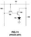
- FIG. 11shows an equivalent circuit diagram of one pixel in a conventional light emitting element display.
- two transistors 103 and 104are connected to a selection scan line 101 and signal line 102 per pixel.
- One and the other of the source and drain electrodes of the transistor 104are connected to an emission voltage line 106 having a positive constant voltage and to an anode of a light emitting element 105 , respectively.
- the selection scan line 101when the selection scan line 101 is selected (when the transistor 103 which is an N-channel transistor is turned on by applying a high-level voltage to the selection scan line 101 ), a signal voltage is applied from the signal line 102 to the gate electrode of the transistor 104 via the transistor 103 . Accordingly, the transistor 104 is turned on, an electric current flows from the emission voltage line 106 to the light emitting element 105 via the transistor 104 , and thus the light emitting element 105 emits light.
- the selection scan line 101is unselected, the transistor 103 is turned off, and the voltage of the gate electrode of the transistor 104 is held. An electric current flows from the light emission voltage line 106 to the light emitting element 105 via the transistor 104 , and the light emitting element 105 emits light.
- the magnitude of an electric current flowing between the drain and source of the transistor 104is adjusted by adjusting the magnitude of the gate-source voltage of the transistor 104 , i.e., the voltage of the signal line 102 . That is, the magnitude of the drain-source current of the transistor 104 is adjusted by using an unsaturated gate voltage as the voltage applied to the gate of the transistor 104 , thereby adjusting the magnitude of the electric current flowing in the transistor 104 and light emitting element 105 . Consequently, the luminance of the light emitting element 105 is adjusted, and tone display is performed.
- This driving methodis called a voltage driving method by which the luminance tone is controlled by modulation of the output signal voltage from the signal line 102 to the transistor 103 .
- the channel resistances of the transistors 103 and 104depend upon the ambient temperature and change after a long-term operation. Therefore, it is difficult to display images with a desired luminance tone for long time periods. Also, if the channel layers of the transistors 103 and 104 are made of polysilicon, the channel resistances depend upon the numbers of grain boundaries as the interfaces between adjacent crystal grains in these channel layers. This may vary the numbers of crystal grains in the channel layers of a plurality of transistors 103 and a plurality of transistors 104 formed in a single panel. Especially when the grain size is increased to obtain high mobility, the number of grain boundaries in the channel layer inevitably decreases, so even a slight difference between the numbers of grain boundaries in the channel length direction has a large effect on the channel resistance.
- a plurality of transistorsare combined as active elements formed in each pixel.
- a p-channel transistor and n-channel transistorare combined.
- a polysilicon transistorfunctions as a p-type transistor.
- an amorphous silicon transistoris used, however, good physical properties with which the transistor functions well cannot be obtained. This makes it impossible to apply amorphous silicon transistors which can be fabricated at a relatively low cost.
- an active elementis made up of four or more transistors in one pixel. If these transistors are formed on a substrate, the upper surface is made uneven by the thicknesses of these transistors. Therefore, an organic EL layer is desirably formed on a flat portion other than the transistor formation region. In this case, no light is emitted in this transistor formation region, so a non-light-emitting portion is inevitably formed in the pixel.
- the brightnesscan be roughly set by (emission luminance per unit area) ⁇ (emission area of one pixel) ⁇ (emission time).
- the emission area of one pixeldecreases. To compensate for this small emission area, the emission luminance per unit area must be increased. Unfortunately, this shortens the light emission life because the organic EL layer is applied with a higher voltage and current. In addition, when the number of transistors in one pixel increases, the fabrication yield lowers exponentially.
- one advantage of the present inventionis that pixels stably display images with desired luminance in a display panel.
- Another advantage of the present inventionis that the display area per pixel of a display panel is increased.
- one or more optical elementswhich have a pair of electrodes and exhibit an optical operation corresponding to an electric current flowing between the pair of electrodes;
- one or more switch circuitswhich supply a memory current having a predetermined current value to the current line during a selection period, and stop supply of a current to the current line during a non-selection period;
- one or more current memory circuitswhich store current data corresponding to the current value of the memory current flowing through the current line during the selection period and, in accordance with the current data stored during the selection period, supply a display current having a current value substantially equal to the memory current to the optical element during the non-selection period.
- the current memory circuitstores the current data corresponding to the current value of the memory current flowing during the selection period. Accordingly, the display current having a current value substantially equal to the memory current can be supplied to the optical element. Current control is thus performed by the current values, not by voltage values. This suppresses the influence of variations in the voltage-current characteristic of the control system and allows the optical element to stably display images with desired luminance.
- the current memory circuithas only one current control transistor connected in series with the optical element. With this arrangement, the voltage between the optical element and current memory circuit is divided only by the optical element and current control transistor. This achieves a low voltage and consequently low power consumption driving.
- each pixelcan operate by using the three transistors, i.e., the current control transistor, current data write control transistor, and current path control transistor.
- Thisdecreases the number of transistors in one pixel and increases the area occupied by the optical element. Decreasing the number of transistors in one pixel also decreases a reduction in the fabrication yield.
- the ratio of the light emission area in the pixelcan be increased, and the apparent brightness improves accordingly. Therefore, the value of an electric current flowing per unit area can be decreased to a relatively small value. This suppresses deterioration of the EL element caused by an injection current.
- a display panel driving methodcomprises:
- FIG. 1is block diagram showing a practical arrangement of a light emitting element display to which the present invention is applied;
- FIG. 2is a plan view schematically showing one pixel of the light emitting element display
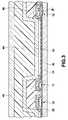
- FIG. 3is a sectional view showing a section taken along a line III-III in FIG. 2 ;
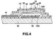
- FIG. 4is a sectional view showing a transistor surrounded by a line IV in FIG. 3 ;
- FIG. 5Ais an equivalent circuit diagram of the pixel of the light emitting element display, showing the driving principle in a selection period
- FIG. 5Bis an equivalent circuit diagram of the pixel of the light emitting element display, showing the driving principle in a non-selection period
- FIG. 6is a graph showing a relationship between an electric current flowing through an n-channel MOSFET connected in series with a light emitting element of the light emitting element display, and a voltage applied to this MOSFET;
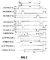
- FIG. 7is a timing chart showing an operation of a driving circuit
- FIG. 8Ais an equivalent circuit diagram of a pixel of another light emitting element display, showing the driving principle in a selection period of the pixel of this light emitting element display
- FIG. 8Bis an equivalent circuit diagram of the pixel of this light emitting element display, showing the driving principle in a non-selection period
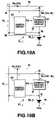
- FIG. 9Ais an equivalent circuit diagram of a pixel of still another light emitting element display, showing the driving principle in a selection period of the pixel of this light emitting element display
- FIG. 9Bis an equivalent circuit diagram of the pixel of this light emitting element display, showing the driving principle in a non-selection period
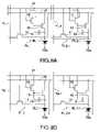
- FIG. 10Ais an equivalent circuit diagram of a pixel of still another light emitting element display, showing the driving principle in a selection period of the pixel of this light emitting element display
- FIG. 10Bis an equivalent circuit diagram of the pixel of this light emitting element display, showing the driving principle in a non-selection period
- FIG. 11is an equivalent circuit diagram showing the circuit configuration of one pixel of a conventional light emitting element display.
- FIG. 1is a block diagram showing a practical arrangement of a light emitting element display to which the present invention is applied.
- the light emitting element display 1includes, as its basic configuration, an active matrix type light emitting panel (driver) 2 and a controller 6 for controlling the whole light emitting display 1 .
- the light emitting element display 1is a so-called active matrix driving type display device.
- the light emitting panel 2includes a transparent substrate 30 (shown in FIG. 3 ) which is made of, e.g., borosilicate glass, silica glass, and another glass which is resistant against temperatures during a transistor fabrication process (to be described later).
- Light emitting unit 7is formed on the transparent substrate 30 , has a plurality of pixels and emits light so as to display an image corresponding to image data from the controller 6 .
- a selection scan driver 3 , emission voltage scan driver 4 , and data driver 5are formed on the transparent substrate 30 and drive the individual pixels of the light emitting unit 7 .
- These selection scan driver 3 , emission voltage scan driver 4 , and data driver 5are so connected as to be able to receive control signals ⁇ s, ⁇ e, and ⁇ d, respectively, and data from the controller 6 .
- Various lines and elementsare formed on the transparent substrate 30 to construct the light emitting panel 2 .
- m selection scan lines X 1 , X 2 , . . . , X mare formed parallel to each other on the transparent substrate 30 .
- m emission voltage scan lines Z 1 , Z 2 , . . . , Z mare formed on the transparent substrate 30 so as to alternate with the selection scan lines X 1 , X 2 , . . . , X m , respectively.
- These emission voltage scan lines Z 1 , Z 2 , . . . , Z mare parallel to and separated from the selection scan lines X 1 , X 2 , . . . , X m .
- current lines Y 1 , Y 2 , . . . , Y nare formed on the transparent substrate 30 substantially perpendicularly to the selection scan lines X 1 , X 2 , . . . , X m and emission voltage scan lines Z 1 , Z 2 , . . . , Z m .
- Y nare made of chromium, chromium alloy, aluminum, aluminum alloy, titanium, titanium alloy, or a low-resistance material selected from at least one of these materials.
- the selection scan lines X 1 , X 2 , . . . , X m and emission voltage scan lines Z 1 , Z 2 , . . . , Z mcan be formed by patterning the same conductive film.
- the current lines Y 1 , Y 2 , . . . , Y nare formed to cross the selection scan lines X 1 , X 2 , . . . , X m and emission voltage scan lines Z 1 , Z 2 , . . . , Z m .
- the selection scan lines X 1 , X 2 , . . . , X m and emission voltage scan lines Z 1 , Z 2 , . . . , Z mare insulated from the current lines Y 1 , Y 2 , . . . , Y n by, e.g., a gate insulating film 32 or semiconductor layer 33 (to be described later).
- a plurality of organic EL elements ijare arrayed in a matrix manner on the transparent substrate 30 .
- One organic EL elementis formed in each of the regions surrounded by the current lines Y 1 , Y 2 , . . . , Y n and selection scan lines X 1 , X 2 , . . . , X m .
- a driving circuit for supplying a predetermined electric current to each organic EL elementis formed around each organic EL element.
- One organic EL element and the driving circuit corresponding to this elementform one pixel Pij of the light emitting unit 2 . That is, one organic EL element is formed for each of (m 33 n) pixels.
- FIG. 2is a plan view showing the major components of one pixel of this light emitting unit 2 .
- FIG. 3is a sectional view taken along line III in FIG. 2 .
- FIG. 4is a sectional view showing a region surrounded by a line IV in FIG. 3 in an enlarged scale.
- FIGS. 5A and 5Bare equivalent circuit diagrams showing driving of two adjacent pixels P i,j and P i,j+1 .
- a gate insulating film 32 , first impurity doped layer 34 , second impurity doped layer 35 , block insulating film 36 , cathode electrode 43 , and the likeare at least partially omitted.
- hatchingis partially omitted to make the drawing readily understandable.
- the organic EL element E i,jis formed in a region surrounded by the selection scan line X i , current line Y j , selection scan line X i+1 (i.e., a selection scan line positioned in the lower stage of the selection scan line X i , and positioned below the emission voltage scan line Z i ; not shown), and current line Y j+1 (i.e., a signal line to the right of the current line Y j ; not shown).
- a capacitor 13 and three transistors 10 , 11 , and 12 as n-channel amorphous silicon thin film transistorsare formed.
- a pixel driving circuit D i,j for driving the organic EL element E i,jincludes the transistors 10 , 11 , and 12 , capacitor 13 , and the like.
- iis an integer from 1 to m
- jis an integer from 1 to n. That is, the “selection scan line X i ” means a selection scan line in the ith row, the “emission voltage scan line Z i ” means an emission voltage scan line in the ith row, and the “current line Y j ” means a signal line in the jth column.
- the “pixel driving circuit D i,j ”means a driving circuit of a pixel P i,j in the ith row and jth column
- the “organic EL element E i,j ”means an organic EL element of this pixel P i,j in the ith row and jth column.
- G, S, and D attached to reference numerals 10 , 11 , and 12mean the gate, source, and drain, respectively, of a transistor.
- the transistor 12has a gate electrode (control terminal) 12 G, a gate insulating film 32 formed on the entire surface of the light emitting unit 7 , a semiconductor layer 33 for forming a single channel as a current path, a first impurity doped layer 34 , a second impurity doped layer 35 , a block insulating film 36 , a drain electrode 12 D, a source electrode 12 S, and a protective insulating film 39 .
- the gate electrode 12 Gis formed on the transparent substrate 30 .
- the gate electrode 12 Gis made of chromium, chromium alloy, aluminum, aluminum alloy, titanium, titanium alloy, or a low-resistance material selected from at least one of these materials.
- the gate insulating film 32is formed on the gate electrode 12 G and transparent substrate 30 so as to cover these gate electrode 12 G and transparent substrate 30 .
- the gate insulating film 32is made of, e.g., silicon nitride or silicon oxide which transmits light and has insulating properties.
- the gate insulating film 32also covers the gate electrodes of other transistors (all transistors formed on the transparent substrate 30 ), the selection scan lines X 1 , X 2 , . . . , X m , and the emission voltage scan lines Z 1 , Z 2 , . . . , Z m .
- the semiconductor layer 33opposes the gate electrode 12 G via the part of the gate insulating film 32 (i.e., the semiconductor layer 33 is formed immediately above the gate electrode 12 G).
- This semiconductor layer 33is made of intrinsic amorphous silicon.
- the block insulating film 36made of silicon nitride is formed.
- the first and second impurity doped layers 34 and 35are formed to be separated from each other on one and the other side portions of the block insulating film 36 .
- the first impurity doped layer 34covers one side portion of the semiconductor layer 33 and one side portion of the block insulating film 36 .
- the second impurity doped layer 35covers the other side portion of the semiconductor layer 33 and the other side portion of the block insulating film 36 .
- These first and second doped layers 34 and 35are made of amorphous silicon doped with n-type impurity ions.
- the drain electrode 12 Dis formed on the first impurity doped layer 34
- the source electrode 12 Sis formed on the second impurity doped layer 35 .
- These drain electrode 12 D and source electrode 12 Sare made of chromium, chromium alloy, aluminum, aluminum alloy, titanium, titanium alloy, or a low-resistance material selected from at least one of these materials, and have a function of blocking the transmission of visible light. This prevents the incidence of light from the outside or from the organic EL element E i,j onto the semiconductor layer 33 and first and second impurity doped layers 34 and 35 .
- the source electrode 12 S and drain electrode 12 Dare electrically insulated from each other.
- the source electrode 12 Sis electrically connected to an anode electrode 41 (to be described later) of the EL element.
- the protective insulating film 39covers the transistors 10 , 11 , and 12 , capacitor 13 , selection scan lines X 1 , X 2 , . . . , X m , current lines Y 1 , Y 2 , . . . , Y n , and emission voltage scan lines Z 1 , Z 2 , . . . , Z m , and exposes the anode electrode 41 . That is, the protective insulating film 39 is so formed as to cover the surroundings of the anode electrode 41 in a matrix manner.
- the transistor 12 constructed as aboveis an MOS field-effect transistor having the semiconductor layer 33 as a channel region. Since the transistors 10 and 11 have substantially the same structure as the transistor 12 , a detailed description thereof will be omitted.
- One electrode of the capacitor 13is the gate electrode 12 G of the transistor 12
- the other electrode of the capacitor 13is the source electrode 12 S of the transistor 12 . Since the gate insulating film 32 formed between the two electrodes of the capacitor 13 is made of a dielectric material, this capacitor 13 functions as a capacitor in which current data corresponding to the value of an electric current flowing between the source and drain of the transistor 12 is written. That is, the capacitor 13 functions as a parasitic capacitance in the gate-to-source path of the transistor 12 and stores the written current data.
- the source 10 S of the transistor 10 and the gate 12 G of the transistor 12are connected via a plurality of openings 47 formed in the gate insulating film 32 .
- the drain 12 D of the transistor 12is connected to one of the emission voltage scan lines Z 1 , Z 2 , . . . , Z m via a plurality of openings 48 formed in the gate insulating film 32 .
- a metal film deposited on the transparent substrate 30is first patterned to form the gate electrodes of the transistors 10 , 11 , and 12 , the selection scan lines X 1 , X 2 , . . . , X m , and the emission voltage scan lines Z 1 , Z 2 , . . . , Z m in the same step.
- a gate insulating film 32 of the transistors 10 , 11 , and 12is formed on the entire surface, and a semiconductor layer 33 , block insulating film 36 , and impurity doped layers 34 and 35 are formed in accordance with their respective shapes.
- a metal film deposited on top of these componentsis patterned to form a source electrode 10 S and drain electrode 10 D of the transistor 10 , a source electrode 11 S and drain electrode 11 D of the transistor 11 , a source electrode 12 S and drain electrode 12 D of the transistor 12 , and current lines Y 1 , Y 2 , . . . , Y n in the same step. At the intersections of the current lines Y 1 , Y 2 , . .
- the block insulating film 36is interposed in addition to the gate insulating film 32 .
- a protective insulating film 39is formed by patterning.
- a channel width W or channel length L of the semiconductor layer 33 of each of the three transistors 10 , 11 , and 12is appropriately set in accordance with the transistor characteristics of that transistor.
- the protective insulating film 39is covered with an insulating partition wall 46 made of, e.g., silicon nitride ( FIG. 3 ).
- the partition wall 46has openings in positions corresponding to the anode electrodes 41 surrounded by the current lines Y 1 , Y 2 , . . . , Y n parallel in the longitudinal direction, and the selection scan lines X 1 , X 2 , . . . , X m and emission voltage scan lines Z 1 , Z 2 , . . . , Z m parallel in the lateral direction.
- the organic EL element E i,jis formed in each of regions partitioned in a matrix manner by the partition wall 46 , i.e., in each of regions surrounded by the current lines Y 1 , Y 2 , . . . , Y n , selection scan lines X 1 , X 2 , . . . , X m , and emission voltage scan lines Z 1 , Z 2 , . . . , Z m .
- the partition wall 46is formed after the formation of the transistors 10 , 11 , and 12 , capacitor 13 , selection scan lines X 1 , X 2 , . . . , X m , current lines Y 1 , Y 2 , . . . , Y n , and emission voltage scan lines Z 1 , Z 2 , . . . , Z m .
- this organic EL element E i,jincludes the anode electrode 41 , an organic EL layer 42 , and a cathode electrode 43 .
- the organic EL layer 42 and cathode electrode 43are stacked in this order from the anode electrode 41 .
- the anode electrode 41is formed on the gate insulating film 32 in each of the regions surrounded by the current lines Y 1 , Y 2 , . . . , Y n and selection scan lines X 1 , X 2 , . . . , X m .
- This anode electrode 41preferably injects holes efficiently into the organic EL layer 42 .
- the main component of the material of this anode electrode 41are tin-doped indium oxide (ITO), zinc-doped indium oxide (IZO), indium oxide (In 2 O 3 ), tin oxide (SnO 2 ), and zinc oxide (ZnO).
- the anode electrode 41is formed before the formation of the source electrode 12 S of the transistor 12 . After this anode electrode 41 is formed, the source electrode 12 S of the transistor 12 is formed, and the protective insulating film 39 is formed after that.
- the organic EL layer 42is formed on the anode electrode 41 .
- This organic EL layer 42can have any of a three-layered structure in which a hole transporting layer, light emitting layer, and electron transporting layer are stacked in this order from the anode electrode 41 , a two-layered structure in which a hole transporting layer and light emitting layer are stacked in this order from the anode electrode 41 , a single-layered structure having only a light emitting layer, and some other layer arrangement.
- the organic EL layer 42has a function of injecting holes and electrons, a function of transporting holes and electrons, and a function of emitting light by generating excitons by recombination of holes and electrons.
- This organic EL layer 42is desirably an electronically neutral organic compound.
- the organic EL layer 42like this achieves well-balanced injection and transportation of holes and electrons.
- This light emitting layer of the organic EL layer 42contains a light emitting material.
- a high-molecular materialis used as this light emitting material.
- the high-molecular materialare polycarbazole-based, polyparaphenylene-based, polyarylenevinylene-based, polythiophene-based, polyfluorene-based, polysilane-based, polyacetylene-based, polyaniline-based, polypyridine-based, polypyridinevinylene-based, and polypyrrol-based materials.
- the high-molecular materialexamples include a polymer or copolymer of a monomer or oligomer forming the above-mentioned high-molecular material (polymer), a polymer or copolymer of a derivative of the monomer or oligomer, and a polymer or copolymer obtained by polymerizing a monomer having oxazole (oxandiazole, triazole, or diazole) or a triphenylamine skeleton.
- Monomers of these polymersinclude monomers and precursor polymers which form the aforementioned compounds when given heat, pressure, UV, or electron beams. It is also possible to introduce a non-conjugate unit which combines these monomers.
- polyfluorenepolyfluorene
- polyvinylcarbazolepolytodecylthiophene (?)
- polyethylenedioxythiophenea polystyrenesulfonic acid dispersed modified product
- poly9,9-dialkylfluorenepoly(thienylene-9,9-dialkylfluorene)
- polyparaphenylenevinylenepoly(2-methoxy-5-(2′-ethylhexyloxy)-paraphenylenevinylene), poly(2-methoxy-5-(2′-ethyl-pentyloxy)-paraphenylenevinylene), poly(2,5-dimethyl-paraphenylenevinylene), poly(2,5-thienylenevinylene), poly(2,5-dimethoxyparaphenylenevinylene), and poly(1,4-paraphen
- a film of a low-molecular materialinstead of the high-molecular material, can also be formed by evaporation.
- the low-molecular materialcan be dissolved in a solvent and used by coating.
- a low-molecular materialcan be dispersed as a dopant in a polymer.
- low-molecular light emitting materialexamples include anthracene, naphthalene, phenanthrene, pyrene, tethracene, coronene, chrysene, fluoresceine, perylene, phthaloperylene, naphthaloperylene, perinone, phthaloperinone, naphthaloperinone, diphenylbutadiene, tetraphenylbutadiene, coumarin, oxadiazole, aldazine, bisbenzoquizoline (?), bisstyryl, pyrazine, oxine, aminoquinoline, imine, diphenylethylene, vinylanthracene, diaminocarbazole, pyran, thiopyran, polymethine, merocyanine, an imidazole chelated oxynoid compound, 4-dicyanomethylene-4H-pyran, 4-dicyanom
- the light emitting materialis not limited to those enumerated above.
- Examples of the electron transporting material contained in the light emitting layer or electron transporting layerare a quinoline derivative, e.g., 8-quinolinol such as tris(8-quinolinolato)aluminum(Alq3) or an organic metal complex having a derivative of this 8-quinolinol as a ligand, an oxadiazole derivative, a perylene derivative, a pyridine derivative, a pyrimidine derivative, a quinoxaline derivative, a diphenylquinone derivative, and a nitro-substituted fluorene derivative.
- 8-quinolinolsuch as tris(8-quinolinolato)aluminum(Alq3) or an organic metal complex having a derivative of this 8-quinolinol as a ligand, an oxadiazole derivative, a perylene derivative, a pyridine derivative, a pyrimidine derivative, a quinoxaline derivative, a di
- Examples of the hole transporting material contained in the light emitting layer or hole transporting layerare a tetraarylbenzicine (?) compound (triaryldiamine or triphenyldiamine: TPD), aromatic tertiary amine, a hydrazone derivative, an imidazole derivative, an oxadiazole derivative having an amino group, and polythiophene.
- a tetraarylbenzicine (?) compoundtriaryldiamine or triphenyldiamine: TPD
- aromatic tertiary aminearomatic tertiary amine
- a hydrazone derivativean imidazole derivative
- an oxadiazole derivative having an amino groupand polythiophene.
- the cathode electrode 43is formed on the organic EL layer 42 .
- This organic EL layer 42is so formed as to extend on the partition wall 46 , and the cathode electrode 43 is a layer shared by all the organic EL elements E 1,1 to E m,n formed in the light emitting unit 2 .
- This cathode electrode 43is made of a material having excellent electron injection properties and a small work function. More specifically, it is preferable to combine at least one metal selected from lithium, indium, magnesium, calcium, barium, and a rare earth element and a low-resistance material such as gold, silver, copper, aluminum, and chromium. More preferably, the low-resistance material is formed on the low-work-function material.
- a shielding layer 44such as silicone oil or an organic insulating material which shields water and oxygen is formed on the cathode electrode 43 on the entire panel surface.
- a sealing layer 45made of a transparent material such as silica glass or some other glass or a transparent material such as resin is formed on the shielding layer 44 .
- the shielding layer 44 and sealing layer 45protect the organic EL elements E i,j , pixel driving circuits D i,j , selection scan lines X 1 , X 2 , . . . , X m , emission voltage scan lines Z 1 , Z 2 , . . . , Z m , and current lines Y 1 , Y 2 , . . . , Y n .
- the gate electrode 10 G of the transistor 10is connected to the selection scan line X i .
- the drain electrode 10 D of the transistor 10is connected to the drain electrode 12 D of the transistor 12 and to the emission voltage scan line Z i .
- the source electrode 10 S of the transistor 10is connected to the gate electrode 12 G of the transistor 12 and to one terminal of the capacitor 13 .
- the source electrode 12 S of the transistor 12is connected to the other terminal of the capacitor 13 and the drain electrode 11 D of the transistor 11 , and to the anode electrode 41 of the organic EL element E i,j .
- the gate electrode 11 G of the transistor 11is connected to the selection scan line X i .
- the source electrode 11 S of the transistor 11is connected to the current line Y j .
- a reference potential V SSis supplied to the cathode electrode of the organic EL element E i,j .
- a voltage V NSE applied to the emission voltage scan line Z i during a non-selection period(to be described in detail later) is equal to or higher than the reference potential V SS .
- a voltage V SE applied to the emission voltage scan line Z i during a selection periodis equal to or lower than the reference potential V SS .
- this reference potential V SSis the ground potential.
- the selection scan driver 3is connected to the selection scan lines X 1 to X m of the light emitting unit 2 .
- This selection scan driver 3is a so-called shift register.
- the selection scan driver 3sequentially outputs scan signals to the selection scan lines in turn from the selection scan line X 1 to the selection scan line X m (after this selection scan line X m , to the selection scan line X 1 ), thereby sequentially selecting the transistors 10 and 11 connected to these selection scan lines X 1 to X m .
- the selection scan driver 3selectively applies a selection scan signal at a high-level ON voltage V ON (much higher than the reference potential V SS ) or low-level OFF voltage V OFF (equal to or lower than the reference potential V SS ) to the selection scan lines X 1 to X m .
- the selection scan driver 3outputs a pulse of the ON voltage V ON to this selection scan line X i , thereby turning on the transistors 11 and 12 (the transistors 11 and 12 of all of the pixel driving circuits D i,1 to D i,n ) connected to the selection scan line X i .
- the selection scan driver 3applies the OFF voltage V OFF to the selection scan line X i to turn off these transistors 11 and 12 .
- the selection periods of the selection scan lines X 1 to X mdo not overlap each other.
- the emission voltage scan driver 4is connected to the emission voltage scan lines Z 1 to Z m of the light emitting unit 2 .
- This emission voltage scan driver 4is a so-called shift register. That is, in accordance with the control signals ⁇ e output from the controller 6 , the emission voltage scan driver 4 sequentially outputs pulse signals to the emission voltage scan lines in turn from the emission voltage scan line Z 1 to the emission voltage scan line Z m (after this emission voltage scan line Z m , to the emission voltage scan line Z 1 ). More specifically, the emission voltage scan driver 4 applies a selection voltage (e.g., 0 [V] if the reference potential is the ground potential) equal to or lower than the reference potential V SS to the emission voltage scan lines Z 1 to Z m at a predetermined cycle.
- a selection voltagee.g., 0 [V] if the reference potential is the ground potential
- the emission voltage scan driver 4applies a low-level selection voltage to the emission voltage scan line Z 1 .
- the emission voltage scan driver 4applies the high-level, non-selection voltage V NSE higher than the reference potential V SS to the emission voltage scan line Z i .
- This non-selection voltage V NSEcan be a negative voltage as long as it is higher than the reference potential V SS , but has a sufficiently large value by which a source-drain voltage V DS of the transistor 12 reaches a saturated region. Details of the saturated voltage will be explained later.
- the controller 6outputs the control signals ⁇ s, ⁇ e, and ⁇ d to the selection driver 3 , emission scan driver 4 , and data driver 5 , respectively.
- the data driver 5is a current sink type driver which receives the control signals from the controller 6 and draws, from the current lines Y 1 to Y n , memory currents flowing to the data driver 5 . That is, this data driver 5 has a current sink circuit and, as indicated by the arrows shown in FIG. 5A , gives rise to memory currents in the current lines Y 1 to Y n .
- the current value of a display current flowing when the organic EL elements E 1,1 to E m,n emit light in the non-selection periodis equal to the current value of the memory current.
- the data driver 5stores electric charge, as current data, which has a magnitude corresponding to the current value of this memory current, in each capacitor 13 .
- FIG. 6is a graph showing the current-voltage characteristics of the transistor 12 as an n-channel MOSFET.
- the abscissaindicates the drain-source voltage value
- the ordinateindicates the drain-source current value.
- the source-drain current value I DSis substantially constant.
- the gate-source current value I DSis represented by
- I DS⁇ ⁇ ⁇ C 0 ⁇ Z 2 ⁇ L ⁇ ( V GS - V TH ) 2 ( 1 )
- ⁇is the mobility of carriers (electrons)
- C 0is a capacitance having an MOS structure gate insulating film as a dielectric
- Zis a channel width
- Lis a channel length.
- the source-drain current value I DSchanges when the source-drain voltage value V DS slightly changes.
- the drain-source current value I DSis unconditionally determined if the gate-source voltage value V GS is determined.
- the drain-source current level I DSis set at the level of a current flowing between the anode electrode 41 and cathode electrode 43 of the organic EL element E i,j which emits light at the maximum luminance.
- a period of T SEis the selection period
- a period of T NSEis a non-selection period
- the selection scan driver 3sequentially outputs high-level (ON-level) pulses to the selection scan lines in turn from the selection scan line X 1 in the first row to the selection scan line X m in the mth row.
- the emission voltage scan driver 4sequentially outputs low-level pulses to the emission voltage scan lines in turn from the emission voltage scan line Z 1 in the first row to the emission voltage scan line Z m in the mth row.
- the high-level voltage output timing of the selection scan line X iis substantially the same as the low-level pulse output timing of the emission voltage scan line Z i .
- the duration of the high-level voltage of the selection scan line X iis substantially the same as that of the low-level voltage of the emission voltage scan line Z i .
- a period during which the high-level pulse and low-level pulse are outputis the selection period T SE of that row.
- the data driver 5generates memory currents (i.e., electric currents flowing toward the data driver 5 ) in the current lines Y 1 to Y n in all columns in accordance with the control signals ⁇ d output from the controller 6 . That is, the data driver 5 supplies a memory current to the current line Y j in each column by a current value corresponding to the image data received by the controller 6 .
- the selection scan driver 3outputs an ON-level (high-level) voltage to the selection scan line X i in the ith row.
- a scan signal voltage V ON at a level by which the transistors 10 and 11 are turned onis applied to the selection scan line X i .
- a selection voltage V SE equal to or lower than the reference voltage V SSis applied to the emission voltage scan line Z i .
- the data driver 5supplies a memory current having a predetermined current value in accordance with the image data received by the controller 6 .
- the transistor 10is turned on to allow an electric current to flow from the drain to the source, and a voltage is applied to the gate of the transistor 12 and one terminal of the capacitor 13 , thereby turning on the transistor 12 .
- the transistor 11is turned on, and the data driver 5 supplies memory currents corresponding to the image data to the current lines Y 1 , Y 2 , . . . , Y j , Y j+1 , . . . , Y n . To supply the memory currents to these current lines Y 1 , Y 2 , . . . , Y j , Y j+1 , . . .
- the data driver 5sets the current lines Y 1 , Y 2 , . . . , Y j , Y j+1 , . . . , Y n at a voltage equal to or lower than the selection voltage V SE and equal to or lower than the reference voltage V SS , thereby making the potential of the source 12 S of the transistor 12 lower than that of the drain.
- memory currents I 1 , I 2 , . . . , I j , I j+1 , . . . , I n having current values (i.e., current values corresponding to the image data) designated by the data driver 5flow through the current lines Y 1 , Y 2 , . . . , Y j , Y j+1 , . . . , Y n in directions indicated by arrows a.
- the selection voltage V SE of the emission voltage scan line Z iis equal to or lower than the reference voltage V SS , and the anode potential of the organic EL element E i,j becomes lower than that of its cathode potential. So, a reverse bias voltage is applied to this organic EL element E i,j . Consequently, no electric current from the emission voltage scan line Z i flows through the organic EL element E i,j .
- the potential of the other terminal (connected to the source electrode 12 S of the transistor 12 ) of the capacitor 13 of each of the pixels P i,1 to P i,ncorresponds to the current value (designated) controlled by the data driver 5 , and is lower than the gate potential of the transistor 12 . That is, electric charge which produces potential differences between the gates and sources of the transistors 12 , by which the electric currents I 1 to I n flow through these transistors 12 of the pixels P i,1 to P i,n , is charged in the capacitors 13 of these pixels P i,1 to P i,n .
- the potential at a given point on, e.g., a line from the transistor 12 to the current line Y jchanges in accordance with, e.g., those internal resistances of the transistors 11 and 12 , which change with time.
- an electric current which flows under the current control of the data driver 5exhibits a predetermined current value.
- the predetermined current value of the electric current flowing in the arrow a directionremains unchanged.
- the organic EL element E i,jinevitably deteriorates with time, i.e., its resistance gradually rises for long time periods, and this gradually raises the divided voltage in this organic EL element E i,j .
- a voltage applied to a transistor connected in series with the organic EL element E i,jmay lower relative to the transistor.
- V Edenote the maximum internal voltage of the organic EL element E i,j , which is required to allow this organic EL element E i,j to emit light at the maximum luminance during its emission life period.
- equation (2) belowis met so that the source and drain of the transistor 12 maintain the saturated region, i.e., the source-drain current I DS of the transistor 12 is controlled only by the gate-source voltage V GS of the transistor 12 , independently of the source-drain voltage V DS of the transistor 12 , even when the gate-source voltage V GS of the transistor 12 is V GSMAX V NSE ⁇ V E ⁇ V SS ⁇ V THMAX (2) where V THMAX is a source-drain saturated threshold voltage of the transistor 12 when V GS is V GSMAX .
- This voltage V THMAXis set at a voltage which is expected to be the highest within the range over which the transistor 12 normally operates when V GSMAX is supplied to the gate of this transistor 12 , by taking account of this displacement of the saturated threshold value when the transistor 12 deteriorates with time and of variations in the characteristics of a plurality of transistors 12 of the light emitting panel 2 .
- the two terminals of the capacitor 13maintain the electric charge charged during the selection period T SE , and the transistor 12 keeps being ON. That is, the gate-source voltage value V GS of the transistor 12 in the non-selection period T NSE is equal to that in the selection period T SE before this non-selection period T SE . Therefore, the transistor 12 keeps allowing the display current, which is equal to the memory current having the current value corresponding to the image data during the selection period T SE , to flow even in the non-selection period T NSE . However, the transistor 11 is OFF.
- the data driver 5forcedly supplies the memory current between the source and drain of the transistor 12 through the current line Y j in accordance with the image data.
- the data driver 5supplies the display current equal to the extracted memory current to the organic EL element E i,j . Accordingly, even when the characteristics of the transistor 12 vary or the characteristics change by deterioration with time, this transistor 12 can supply a desired electric current corresponding to the image data. In addition, a desired electric current flows in the organic EL element E i,j even when the resistance of this organic EL element E i,j rises with time, so stable luminance tone display can be performed.
- the transistor 12 as a current controlling transistoris the only transistor connected in series with the organic EL element E i,j . Therefore, the voltage applied to the emission voltage scan line Z i is divided only by the organic EL element E i,j and transistor 12 . This achieves a low voltage, and as a consequence, low consumption driving. This can also decrease the number of transistors in one pixel to increase the area occupied by an optical element.
- the selection period T SE of the selection scan line X iis completed, the selection period T SE of the selection scan line X i+1 is started subsequently.
- the selection scan driver 3 , emission voltage scan driver 4 , data driver 5 , and controller 6operate in the same manner as for the selection scan line X i .
- the organic EL elements E 1,1 to E 1,n , E 2,1 to E 2,n , . . . , E m,1 to E m,nare linearly selected in turn.
- the selection period T SE of the selection scan line X 1is started again.
- an emission time T EM during which each pixel emits light in one scan period T SCis substantially equivalent to the non-selection period T NSE . As the number of selection scan lines increases, the emission period T EM can be extended.
- the active matrix driving type light emitting element display 1 using current controlcan be implemented by using the three transistors 10 , 11 , and 12 for one pixel P i,j .
- Thisimproves the image characteristics of this light emitting element display 1 . That is, in the active matrix driving type light emitting element display 1 in which the current values are controlled, the present invention can increase the ratio of the light emission area of the pixel P i,j and hence can increase the other design margin. When the ratio of the light emission area increases, the apparent brightness of the display screen of the light emitting element display 1 can be increased. In addition, when an image is displayed with desired apparent brightness, the value of an electric current which flows per unit area of the organic EL layer 42 can be decreased. This can extend the light emission life of the organic EL element E i,j .
- each of the transistors 10 , 11 , and 12 of each pixel driving circuit D i,jis a single-channel type FET with only an n-channel in which a semiconductor layer is formed by amorphous silicon. Accordingly, these transistors 10 , 11 , and 12 can be simultaneously formed on the transparent substrate 30 in the same step. This can suppress an increase in the time or cost for the fabrication of the light emitting panel 2 , light emitting element display 1 , and pixel driving circuit D i,j .
- the same effects as described in the above embodimentcan also be obtained by using p-channel FETs as the transistors 10 , 11 , and 12 . In this case, the individual signals shown in FIG. 7 have opposite phases.
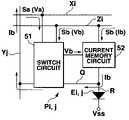
- each pixel P i,j(a pixel driving circuit D i,j of each pixel P i,j ) has a switch circuit 51 instead of transistors 10 and 11 , and a current memory circuit 52 instead of a transistor 12 and capacitor 13 .
- the same reference numerals as in the above first embodimentdenote the same parts, so a detailed explanation thereof will be omitted.
- a power supply signal Sb output to an emission voltage scan line Z ihas a voltage value Vb during a selection period T SE and a voltage value Vb′ during a non-selection period T NSE .
- These voltage values Vb and Vb′correspond to the non-selection voltage V NSE and reference voltage V SS , respectively, shown in FIG. 7 .
- a scan signal Sa output to a selection scan line X ihas a voltage value Va which turns on the switch circuit 51 during the selection period T SE , and a voltage value Va′ which turns off the switch circuit 51 during the selection period T SE .
- This scan signal Sacorresponds to the scan signal (scan signal voltage) shown in FIG. 7 .
- the switch circuit 51outputs the power supply signal Sb from the emission voltage scan line Z i to the current memory circuit 52 in accordance with the scan signal Sa, and supplies an electric current Ib flowing from the current memory circuit 52 to a current line Y through a line Q.
- the current value of this electric current Ibis controlled by a current sink type data driver 5 (i.e., this data driver 5 has a current sink) connected to the current line Y j . Also, as shown in FIG.
- the switch circuit 51stops the supply of a display current from the current memory circuit 52 to the current line Y j in accordance with the scan signal Sa, and supplies this display current to an organic EL element E i,j through a line R. Accordingly, this organic EL element E i,j emits light in the non-selection period T NSE .
- the current memory circuit 52includes a storage means which, during the selection period T SE , allows the electric current Ib controlled by the current sink data driver 5 to flow from the emission voltage scan line Z i to the line Q in accordance with the signal voltage Vb of the power supply signal Sb from the switch circuit 51 , thereby storing the current value of this electric current Ib.
- this current memory circuit 52allows the electric current Ib corresponding to the current value stored by the storage means to flow from the emission voltage scan line Z i to the line R in accordance with the signal voltage Vb′ from the switch circuit 51 . Accordingly, the current value of the electric current Ib during the non-selection period T NSE is equal to or has a linear relationship with the current value of the electric current Ib during the selection period T SE .
- each pixel P i,j of the third embodimenthas a transistor 14 instead of a transistor 10 .
- the same reference numerals as in the above first embodimentdenote the same parts, so a detailed explanation thereof will be omitted.
- a drain electrode 14 D and gate electrode 14 G of the transistor 14are connected to a selection scan line X i , and a source electrode 14 S of this transistor 14 is connected to a gate electrode 12 S of a transistor 12 .
- the transistor 14is an n-channel amorphous silicon thin film transistor.
- This transistor 14operates by the application of a voltage such as that shown in the waveform chart shown in FIG. 7 .
- the transistor 14is turned on by an ON-level (high-level) scan signal from the selection scan line X i to apply a voltage from this selection scan line X i to the gate of the transistor 12 .
- This transistor 12is turned on by the gate voltage applied by the transistor 14 in the selection period T SE , and supplies an electric current I DS (memory current), which is extracted by a data driver 5 having a current sink, via the transistor 11 which is ON and a current line Y j .
- I DSmemory current
- the transistors 11 and 14are turned off by an OFF-level scan signal supplied to the selection scan line X i .
- the transistor 12a predetermined voltage is applied between the source and drain by the voltage value corresponding to the electric charge charged in the capacitor 13 . Accordingly, this transistor 12 supplies a display current corresponding to the voltage value between the source and drain (i.e., corresponding to the electric charge charged in the capacitor 13 ) to an organic EL element E i,j , thereby causing this organic EL element E i,j to emit light.
- the electric current flowing in the organic EL element E i,j in this casehas a current value corresponding to control signals ⁇ s, ⁇ d, and ⁇ e from a controller 6 , i.e., has the current value of the memory current. Therefore, the organic EL element E i,j emits light with luminance corresponding to image data.
- each pixel P i,j(a pixel driving circuit D i,j of each pixel P i,j ) of this fourth embodiment has a switch 53 instead of a switch circuit 51 .
- the same reference numerals as in the above second embodimentdenote the same parts, so a detailed explanation thereof will be omitted.
- the switch 53outputs an ON-level signal (voltage value Va) to a current memory circuit 52 in accordance with a scan signal Sa, and supplies an electric current Ib flowing from this current memory circuit 52 to a current line Y j through a line Q.
- This electric current Ibis controlled by a current sink type data driver 5 (i.e., this data driver 5 has a current sink) connected to the current line Y j .
- the switch 53stops the supply of the electric current Ib from the current memory circuit 52 to the current line Y j in accordance with an OFF-level scan signal (voltage value Va′), and supplies a display current to an organic EL element E i,j through a line R. Accordingly, this organic EL element E i,j emits light in the non-selection period T NSE .
- the present inventionis not limited to the above embodiments. That is, various improvements and design changes can be made without departing from the gist of the present invention.
- an organic EL elementis used as a light emitting element in each of the above embodiments.
- a light emitting elementin which no electric current flows when a reverse bias voltage is applied and an electric current flows when a positive bias voltage is applied, and which emits light with luminance corresponding to the magnitude of the flowing current.
- An exampleis an LED (Light Emitting Diode).
- the transistors 10 , 11 , 12 , and 14 in the above embodimentsare thin film transistors having amorphous silicon as a semiconductor layer (i.e., a channel layer).
- a thin film transistor using a polysilicon semiconductor layercan also be used.
- a capacitor 13 formed by a gate insulating film 32 in which a gate electrode 12 G and source electrode 12 S are stackedis formed between the gate and source of a transistor 12 .
- a capacitor formed by a member not containing at least one of or any of the gate electrode 12 G, source electrode 12 S, and gate insulating film 32can also be formed between the gate and source of the transistor 12 .
Landscapes
- Engineering & Computer Science (AREA)
- Physics & Mathematics (AREA)
- Computer Hardware Design (AREA)
- General Physics & Mathematics (AREA)
- Theoretical Computer Science (AREA)
- Electroluminescent Light Sources (AREA)
- Control Of Indicators Other Than Cathode Ray Tubes (AREA)
- Control Of El Displays (AREA)
Abstract
Description
where μ is the mobility of carriers (electrons), C0is a capacitance having an MOS structure gate insulating film as a dielectric, Z is a channel width, and L is a channel length.
VNSE−VE−VSS≧VTHMAX (2)
where VTHMAXis a source-drain saturated threshold voltage of the
Claims (34)
Applications Claiming Priority (3)
| Application Number | Priority Date | Filing Date | Title |
|---|---|---|---|
| JP2001-400557 | 2001-12-28 | ||
| JP2001400557AJP2003195810A (en) | 2001-12-28 | 2001-12-28 | Driving circuit, driving device, and driving method of optical element |
| PCT/JP2002/013034WO2003058328A1 (en) | 2001-12-28 | 2002-12-12 | Display panel and display panel driving method |
Publications (2)
| Publication Number | Publication Date |
|---|---|
| US20040113873A1 US20040113873A1 (en) | 2004-06-17 |
| US7317429B2true US7317429B2 (en) | 2008-01-08 |
Family
ID=19189629
Family Applications (1)
| Application Number | Title | Priority Date | Filing Date |
|---|---|---|---|
| US10/472,423Expired - LifetimeUS7317429B2 (en) | 2001-12-28 | 2002-12-12 | Display panel and display panel driving method |
Country Status (8)
| Country | Link |
|---|---|
| US (1) | US7317429B2 (en) |
| EP (1) | EP1459126B1 (en) |
| JP (1) | JP2003195810A (en) |
| KR (1) | KR100620976B1 (en) |
| CN (1) | CN1293408C (en) |
| DE (1) | DE60217916T2 (en) |
| TW (1) | TW575860B (en) |
| WO (1) | WO2003058328A1 (en) |
Cited By (52)
| Publication number | Priority date | Publication date | Assignee | Title |
|---|---|---|---|---|
| US20050030265A1 (en)* | 2003-08-08 | 2005-02-10 | Keisuke Miyagawa | Driving method of light emitting device and light emitting device |
| US20050270259A1 (en)* | 2004-06-07 | 2005-12-08 | Casio Computer Co., Ltd. | Display device and method of manufacturing the same |
| US20060098521A1 (en)* | 2004-09-21 | 2006-05-11 | Casio Computer Co., Ltd. | Transistor array substrate and display panel |
| US20100066714A1 (en)* | 2008-09-16 | 2010-03-18 | Casio Computer Co., Ltd. | Display device and driving control method for the same |
| US20100156877A1 (en)* | 2005-06-30 | 2010-06-24 | Semiconductor Energy Laboratory Co., Ltd. | Semiconductor device, display device, and electronic appliance |
| US20100277402A1 (en)* | 2003-08-29 | 2010-11-04 | Seiko Epson Corporation | Electro-optical device, method of driving the same, and electronic apparatus |
| US20110090189A1 (en)* | 2005-08-12 | 2011-04-21 | Semiconductor Energy Laboratory Co., Ltd. | Semiconductor device, display device and electronic device equipped with the semiconductor device |
| US8212750B2 (en) | 2005-12-02 | 2012-07-03 | Semiconductor Energy Laboratory Co., Ltd. | Display device and electronic device |
| US8692748B2 (en)* | 2006-07-27 | 2014-04-08 | Sony Corporation | Display device, driving method thereof, and electronic apparatus |
| US8710505B2 (en) | 2011-08-05 | 2014-04-29 | Semiconductor Energy Laboratory Co., Ltd. | Semiconductor device |
| US8890220B2 (en) | 2001-02-16 | 2014-11-18 | Ignis Innovation, Inc. | Pixel driver circuit and pixel circuit having control circuit coupled to supply voltage |
| USRE45291E1 (en) | 2004-06-29 | 2014-12-16 | Ignis Innovation Inc. | Voltage-programming scheme for current-driven AMOLED displays |
| US8922464B2 (en) | 2011-05-11 | 2014-12-30 | Semiconductor Energy Laboratory Co., Ltd. | Active matrix display device and driving method thereof |
| US9013457B2 (en) | 2012-06-01 | 2015-04-21 | Semiconductor Energy Laboratory Co., Ltd. | Semiconductor device and method for driving semiconductor device |
| US9030105B2 (en) | 2011-04-01 | 2015-05-12 | Semiconductor Energy Laboratory Co., Ltd. | Light-emitting device |
| US9070775B2 (en) | 2011-08-03 | 2015-06-30 | Ignis Innovations Inc. | Thin film transistor |
| US9117409B2 (en) | 2012-03-14 | 2015-08-25 | Semiconductor Energy Laboratory Co., Ltd. | Light-emitting display device with transistor and capacitor discharging gate of driving electrode and oxide semiconductor layer |
| US9134825B2 (en) | 2011-05-17 | 2015-09-15 | Ignis Innovation Inc. | Systems and methods for display systems with dynamic power control |
| US9224954B2 (en) | 2011-08-03 | 2015-12-29 | Ignis Innovation Inc. | Organic light emitting diode and method of manufacturing |
| US9230996B2 (en) | 2013-12-27 | 2016-01-05 | Semiconductor Energy Laboratory Co., Ltd. | Light-emitting device |
| US9257071B2 (en) | 2012-06-01 | 2016-02-09 | Semiconductor Energy Laboratory Co., Ltd. | Semiconductor device and method for driving semiconductor device |
| US9280931B2 (en) | 2011-10-18 | 2016-03-08 | Semiconductor Energy Laboratory Co., Ltd. | Semiconductor device |
| US20160111044A1 (en)* | 2013-06-27 | 2016-04-21 | Sharp Kabushiki Kaisha | Display device and drive method for same |
| US9373645B2 (en) | 2005-01-28 | 2016-06-21 | Ignis Innovation Inc. | Voltage programmed pixel circuit, display system and driving method thereof |
| US9385169B2 (en) | 2011-11-29 | 2016-07-05 | Ignis Innovation Inc. | Multi-functional active matrix organic light-emitting diode display |
| US9502653B2 (en) | 2013-12-25 | 2016-11-22 | Ignis Innovation Inc. | Electrode contacts |
| US9606607B2 (en) | 2011-05-17 | 2017-03-28 | Ignis Innovation Inc. | Systems and methods for display systems with dynamic power control |
| US9633597B2 (en) | 2006-04-19 | 2017-04-25 | Ignis Innovation Inc. | Stable driving scheme for active matrix displays |
| US9666655B2 (en) | 2015-05-05 | 2017-05-30 | Semiconductor Energy Laboratory Co., Ltd. | Display device |
| US9818376B2 (en) | 2009-11-12 | 2017-11-14 | Ignis Innovation Inc. | Stable fast programming scheme for displays |
| US9842889B2 (en) | 2014-11-28 | 2017-12-12 | Ignis Innovation Inc. | High pixel density array architecture |
| US9853068B2 (en) | 2013-12-12 | 2017-12-26 | Semiconductor Energy Laboratory Co., Ltd. | Light-emitting device |
| US9934725B2 (en) | 2013-03-08 | 2018-04-03 | Ignis Innovation Inc. | Pixel circuits for AMOLED displays |
| US9952698B2 (en) | 2013-03-15 | 2018-04-24 | Ignis Innovation Inc. | Dynamic adjustment of touch resolutions on an AMOLED display |
| US9985052B2 (en)* | 2013-12-10 | 2018-05-29 | Semiconductor Energy Laboratory Co., Ltd. | Light-emitting device |
| US10002972B2 (en) | 2015-04-13 | 2018-06-19 | Semiconductor Energy Laboratory Co., Ltd. | OLED display device comprising dual gate transistor |
| US10008149B2 (en) | 2011-07-22 | 2018-06-26 | Semiconductor Energy Laboratory Co., Ltd. | Light-emitting device including pixels suppressing variation in luminance |
| US10043794B2 (en) | 2012-03-22 | 2018-08-07 | Semiconductor Energy Laboratory Co., Ltd. | Semiconductor device and electronic device |
| US10089924B2 (en) | 2011-11-29 | 2018-10-02 | Ignis Innovation Inc. | Structural and low-frequency non-uniformity compensation |
| US10163996B2 (en) | 2003-02-24 | 2018-12-25 | Ignis Innovation Inc. | Pixel having an organic light emitting diode and method of fabricating the pixel |
| US10176752B2 (en) | 2014-03-24 | 2019-01-08 | Ignis Innovation Inc. | Integrated gate driver |
| US10204540B2 (en) | 2015-10-26 | 2019-02-12 | Ignis Innovation Inc. | High density pixel pattern |
| US10373554B2 (en) | 2015-07-24 | 2019-08-06 | Ignis Innovation Inc. | Pixels and reference circuits and timing techniques |
| US10410579B2 (en) | 2015-07-24 | 2019-09-10 | Ignis Innovation Inc. | Systems and methods of hybrid calibration of bias current |
| US10586491B2 (en) | 2016-12-06 | 2020-03-10 | Ignis Innovation Inc. | Pixel circuits for mitigation of hysteresis |
| US10657895B2 (en) | 2015-07-24 | 2020-05-19 | Ignis Innovation Inc. | Pixels and reference circuits and timing techniques |
| US10714018B2 (en) | 2017-05-17 | 2020-07-14 | Ignis Innovation Inc. | System and method for loading image correction data for displays |
| US10971078B2 (en) | 2018-02-12 | 2021-04-06 | Ignis Innovation Inc. | Pixel measurement through data line |
| US10997901B2 (en) | 2014-02-28 | 2021-05-04 | Ignis Innovation Inc. | Display system |
| US11025899B2 (en) | 2017-08-11 | 2021-06-01 | Ignis Innovation Inc. | Optical correction systems and methods for correcting non-uniformity of emissive display devices |
| US12176356B2 (en) | 2011-10-18 | 2024-12-24 | Semiconductor Energy Laboratory Co., Ltd. | Semiconductor device including transistor and light-emitting element |
| US12402496B2 (en) | 2020-12-24 | 2025-08-26 | Semiconductor Energy Laboratory Co., Ltd. | Display device |
Families Citing this family (68)
| Publication number | Priority date | Publication date | Assignee | Title |
|---|---|---|---|---|
| JP2003195810A (en) | 2001-12-28 | 2003-07-09 | Casio Comput Co Ltd | Driving circuit, driving device, and driving method of optical element |
| JP3706107B2 (en)* | 2002-01-18 | 2005-10-12 | 株式会社半導体エネルギー研究所 | LIGHT EMITTING DEVICE AND ELECTRONIC DEVICE |
| JP3939666B2 (en)* | 2002-01-18 | 2007-07-04 | 株式会社半導体エネルギー研究所 | LIGHT EMITTING DEVICE AND ELECTRONIC DEVICE |
| CN101673508B (en) | 2002-01-18 | 2013-01-09 | 株式会社半导体能源研究所 | Light-emitting device |
| JP3918642B2 (en)* | 2002-06-07 | 2007-05-23 | カシオ計算機株式会社 | Display device and driving method thereof |
| JP4610843B2 (en) | 2002-06-20 | 2011-01-12 | カシオ計算機株式会社 | Display device and driving method of display device |
| JP4103500B2 (en)* | 2002-08-26 | 2008-06-18 | カシオ計算機株式会社 | Display device and display panel driving method |
| JP2006072385A (en)* | 2002-10-03 | 2006-03-16 | Seiko Epson Corp | Electronic device and electronic equipment |
| JP2004145300A (en) | 2002-10-03 | 2004-05-20 | Seiko Epson Corp | Electronic circuit, method of driving electronic circuit, electronic device, electro-optical device, method of driving electro-optical device, and electronic apparatus |
| JP3952965B2 (en) | 2003-02-25 | 2007-08-01 | カシオ計算機株式会社 | Display device and driving method of display device |
| JP2004341144A (en)* | 2003-05-15 | 2004-12-02 | Hitachi Ltd | Image display device |
| JP4016962B2 (en)* | 2003-05-19 | 2007-12-05 | セイコーエプソン株式会社 | Electro-optical device and driving method of electro-optical device |
| JP4939737B2 (en)* | 2003-08-08 | 2012-05-30 | 株式会社半導体エネルギー研究所 | Light emitting device |
| CN101488322B (en)* | 2003-08-29 | 2012-06-20 | 精工爱普生株式会社 | Electro-optical device, method of driving the same, and electronic apparatus |
| JP4203656B2 (en) | 2004-01-16 | 2009-01-07 | カシオ計算機株式会社 | Display device and display panel driving method |
| JP4665419B2 (en)* | 2004-03-30 | 2011-04-06 | カシオ計算機株式会社 | Pixel circuit board inspection method and inspection apparatus |
| US7586171B2 (en)* | 2004-04-14 | 2009-09-08 | Yong Cao | Organic electronic device comprising conductive members and processes for forming and using the organic electronic device |
| JP2005311591A (en)* | 2004-04-20 | 2005-11-04 | Matsushita Electric Ind Co Ltd | Current drive |
| US20060007070A1 (en)* | 2004-06-02 | 2006-01-12 | Li-Wei Shih | Driving circuit and driving method for electroluminescent display |
| JP4424078B2 (en)* | 2004-06-07 | 2010-03-03 | カシオ計算機株式会社 | Display panel and manufacturing method thereof |
| JP2005345992A (en)* | 2004-06-07 | 2005-12-15 | Chi Mei Electronics Corp | Display device |
| JP2006010986A (en)* | 2004-06-24 | 2006-01-12 | Kyocera Corp | Image display device |
| JP4599924B2 (en)* | 2004-07-21 | 2010-12-15 | カシオ計算機株式会社 | Thin film transistor and display panel |
| KR100846954B1 (en)* | 2004-08-30 | 2008-07-17 | 삼성에스디아이 주식회사 | Light emitting display device and driving method thereof |
| JP4379278B2 (en)* | 2004-09-21 | 2009-12-09 | カシオ計算機株式会社 | Transistor array substrate and display panel |
| JP5152448B2 (en)* | 2004-09-21 | 2013-02-27 | カシオ計算機株式会社 | Pixel drive circuit and image display device |
| JP4517804B2 (en)* | 2004-09-29 | 2010-08-04 | カシオ計算機株式会社 | Display panel |
| JP4379285B2 (en)* | 2004-09-29 | 2009-12-09 | カシオ計算機株式会社 | Display panel |
| JP4747543B2 (en)* | 2004-09-29 | 2011-08-17 | カシオ計算機株式会社 | Display panel |
| JP4254675B2 (en)* | 2004-09-29 | 2009-04-15 | カシオ計算機株式会社 | Display panel |
| JP4747552B2 (en)* | 2004-10-19 | 2011-08-17 | セイコーエプソン株式会社 | Electro-optical device, electronic apparatus and method |
| KR100583519B1 (en)* | 2004-10-28 | 2006-05-25 | 삼성에스디아이 주식회사 | Scan driver and light emitting display device using same |
| JP4438069B2 (en)* | 2004-12-03 | 2010-03-24 | キヤノン株式会社 | Current programming device, active matrix display device, and current programming method thereof |
| KR100805542B1 (en)* | 2004-12-24 | 2008-02-20 | 삼성에스디아이 주식회사 | Light-emitting display device and driving method thereof |
| WO2006070833A1 (en) | 2004-12-27 | 2006-07-06 | Kyocera Corporation | Image display and its driving method, and driving method of electronic apparatus |
| US7907137B2 (en) | 2005-03-31 | 2011-03-15 | Casio Computer Co., Ltd. | Display drive apparatus, display apparatus and drive control method thereof |
| JP5647757B2 (en)* | 2005-06-30 | 2015-01-07 | 株式会社半導体エネルギー研究所 | Semiconductor device, light emitting device, module, and electronic device |
| JP4788216B2 (en)* | 2005-07-21 | 2011-10-05 | コニカミノルタホールディングス株式会社 | DRIVE DEVICE, DISPLAY DEVICE, DRIVE DEVICE, AND DISPLAY DEVICE DRIVE METHOD |
| KR100667075B1 (en)* | 2005-07-22 | 2007-01-10 | 삼성에스디아이 주식회사 | Scan driver and organic light emitting display device comprising the same |
| KR100729099B1 (en)* | 2005-09-20 | 2007-06-14 | 삼성에스디아이 주식회사 | Scan Driving Circuit and Organic Electroluminescent Device Using the Same |
| JP5364235B2 (en)* | 2005-12-02 | 2013-12-11 | 株式会社半導体エネルギー研究所 | Display device |
| JP4952886B2 (en)* | 2006-03-16 | 2012-06-13 | カシオ計算機株式会社 | Display device and drive control method thereof |
| JP4956031B2 (en)* | 2006-03-31 | 2012-06-20 | キヤノン株式会社 | Drive method and drive circuit for organic EL display device |
| JP4314638B2 (en)* | 2006-08-01 | 2009-08-19 | カシオ計算機株式会社 | Display device and drive control method thereof |
| TWI385621B (en) | 2006-08-01 | 2013-02-11 | Casio Computer Co Ltd | Display drive apparatus and a drive method thereof, and display apparatus and the drive method thereof |
| JP4748456B2 (en)* | 2006-09-26 | 2011-08-17 | カシオ計算機株式会社 | Pixel drive circuit and image display device |
| KR100857672B1 (en)* | 2007-02-02 | 2008-09-08 | 삼성에스디아이 주식회사 | Organic light emitting display device and driving method thereof |
| WO2009078166A1 (en) | 2007-12-19 | 2009-06-25 | Panasonic Corporation | Active matrix type display device |
| US20090201235A1 (en)* | 2008-02-13 | 2009-08-13 | Samsung Electronics Co., Ltd. | Active matrix organic light emitting diode display |
| US20090201278A1 (en)* | 2008-02-13 | 2009-08-13 | Samsung Electronics Co., Ltd. | Unit pixels and active matrix organic light emitting diode displays including the same |
| JP4893753B2 (en)* | 2009-01-08 | 2012-03-07 | カシオ計算機株式会社 | Display panel |
| RU2489756C2 (en) | 2009-05-13 | 2013-08-10 | Шарп Кабушики Каиша | Display device |
| RU2521266C2 (en) | 2009-06-04 | 2014-06-27 | Шарп Кабушики Каиша | Display device and display device control method |
| WO2011030370A1 (en) | 2009-09-08 | 2011-03-17 | パナソニック株式会社 | Display panel device and control method thereof |
| JP2011095720A (en)* | 2009-09-30 | 2011-05-12 | Casio Computer Co Ltd | Light-emitting apparatus, drive control method thereof, and electronic device |
| TWI416491B (en)* | 2009-10-09 | 2013-11-21 | Sumika Technology Co | Pixel circuit and display panel |
| JP5381836B2 (en)* | 2010-03-17 | 2014-01-08 | カシオ計算機株式会社 | Pixel circuit board, display device, electronic apparatus, and display device manufacturing method |
| KR101813192B1 (en)* | 2011-05-31 | 2017-12-29 | 삼성디스플레이 주식회사 | Pixel, diplay device comprising the pixel and driving method of the diplay device |
| US8878589B2 (en) | 2011-06-30 | 2014-11-04 | Semiconductor Energy Laboratory Co., Ltd. | Semiconductor device and driving method thereof |
| KR101953724B1 (en) | 2011-08-26 | 2019-03-04 | 가부시키가이샤 한도오따이 에네루기 켄큐쇼 | Light-emitting module, light-emitting device, method of manufacturing the light-emitting module, and method of manufacturing the light-emitting device |
| JP6050054B2 (en) | 2011-09-09 | 2016-12-21 | 株式会社半導体エネルギー研究所 | Semiconductor device |
| US9711092B2 (en) | 2013-03-14 | 2017-07-18 | Sharp Kabushiki Kaisha | Display device and method for driving same |
| WO2014208458A1 (en) | 2013-06-27 | 2014-12-31 | シャープ株式会社 | Display device and drive method therefor |
| JP6793222B2 (en) | 2013-12-12 | 2020-12-02 | 株式会社半導体エネルギー研究所 | Electronics |
| JP6169191B2 (en) | 2013-12-20 | 2017-07-26 | シャープ株式会社 | Display device and driving method thereof |
| JP6633330B2 (en)* | 2014-09-26 | 2020-01-22 | 株式会社半導体エネルギー研究所 | Semiconductor device |
| CN105372893B (en)* | 2015-12-24 | 2019-01-18 | 信利半导体有限公司 | A kind of pixel-driving circuit, array substrate and liquid crystal display device |
| KR102477486B1 (en)* | 2016-04-19 | 2022-12-14 | 삼성디스플레이 주식회사 | Emission control driver and display device having the same |
Citations (48)
| Publication number | Priority date | Publication date | Assignee | Title |
|---|---|---|---|---|
| JPH01123292A (en) | 1987-11-09 | 1989-05-16 | Matsushita Electric Ind Co Ltd | Inspection of active matrix array |
| JPH08330600A (en) | 1995-03-24 | 1996-12-13 | Tdk Corp | Thin film transistor, organic EL display device, and method for manufacturing organic EL display device |
| US5680149A (en) | 1993-12-25 | 1997-10-21 | Semiconductor Energy Laboratory Co., Ltd. | Driving circuit for driving liquid crystal display device |
| JPH11143429A (en) | 1997-11-10 | 1999-05-28 | Pioneer Electron Corp | Luminous display and its driving method |
| WO1999065011A2 (en) | 1998-06-12 | 1999-12-16 | Koninklijke Philips Electronics N.V. | Active matrix electroluminescent display devices |
| US6023259A (en) | 1997-07-11 | 2000-02-08 | Fed Corporation | OLED active matrix using a single transistor current mode pixel design |
| US6091382A (en) | 1995-12-30 | 2000-07-18 | Casio Computer Co., Ltd. | Display device for performing display operation in accordance with signal light and driving method therefor |
| JP2000221942A (en) | 1999-01-29 | 2000-08-11 | Nec Corp | Organic el element driving device |
| US6166714A (en) | 1996-06-06 | 2000-12-26 | Kabushiki Kaisha Toshiba | Displaying device |
| WO2001006484A1 (en) | 1999-07-14 | 2001-01-25 | Sony Corporation | Current drive circuit and display comprising the same, pixel circuit, and drive method |
| WO2001020591A1 (en) | 1999-09-11 | 2001-03-22 | Koninklijke Philips Electronics N.V. | Active matrix electroluminescent display device |
| US6229506B1 (en) | 1997-04-23 | 2001-05-08 | Sarnoff Corporation | Active matrix light emitting diode pixel structure and concomitant method |
| JP2001147659A (en) | 1999-11-18 | 2001-05-29 | Sony Corp | Display device |
| US20010017618A1 (en) | 1999-12-27 | 2001-08-30 | Munehiro Azami | Image display device and driving method thereof |
| WO2001075852A1 (en) | 2000-03-31 | 2001-10-11 | Koninklijke Philips Electronics N.V. | Display device having current-addressed pixels |
| EP1146501A1 (en) | 1999-10-18 | 2001-10-17 | Seiko Epson Corporation | Display |
| US20010035863A1 (en) | 2000-04-26 | 2001-11-01 | Hajime Kimura | Electronic device and driving method thereof |
| US20010052606A1 (en) | 2000-05-22 | 2001-12-20 | Koninklijke Philips Electronics N.V. | Display device |
| EP1170718A1 (en) | 2000-07-07 | 2002-01-09 | Seiko Epson Corporation | Current sampling circuit for organic electroluminescent display |
| US20020014852A1 (en) | 2000-02-03 | 2002-02-07 | Bae Sung Joon | Driving circuit for electro-luminescence cell |
| US20020075208A1 (en) | 2000-12-15 | 2002-06-20 | Bae Sung Joon | Driving IC of an active matrix electroluminescence device |
| JP2002215095A (en) | 2001-01-22 | 2002-07-31 | Pioneer Electronic Corp | Pixel driving circuit of light emitting display |
| US20020163514A1 (en) | 2000-07-28 | 2002-11-07 | Yoshifumi Nagai | Drive circuit of display and display |
| US20020195968A1 (en) | 2001-06-22 | 2002-12-26 | International Business Machines Corporation | Oled current drive pixel circuit |
| US20030020335A1 (en) | 1998-11-27 | 2003-01-30 | Naoaki Komiya | Electroluminescence display apparatus for displaying gray scales |
| US6522315B2 (en) | 1997-02-17 | 2003-02-18 | Seiko Epson Corporation | Display apparatus |
| US20030098708A1 (en) | 1997-01-29 | 2003-05-29 | Seiko Espon Corporation | Active matrix substrate inspecting method, active matrix substrate, liquid crystal device, and electronic apparatus |
| US20030103022A1 (en)* | 2001-11-09 | 2003-06-05 | Yukihiro Noguchi | Display apparatus with function for initializing luminance data of optical element |
| US20030112205A1 (en)* | 2001-12-18 | 2003-06-19 | Sanyo Electric Co., Ltd. | Display apparatus with function for initializing luminance data of optical element |
| WO2003058328A1 (en) | 2001-12-28 | 2003-07-17 | Casio Computer Co., Ltd. | Display panel and display panel driving method |
| US6661180B2 (en) | 2001-03-22 | 2003-12-09 | Semiconductor Energy Laboratory Co., Ltd. | Light emitting device, driving method for the same and electronic apparatus |
| EP1372136A1 (en) | 2002-06-12 | 2003-12-17 | Seiko Epson Corporation | Scan driver and a column driver for active matrix display device and corresponding method |
| US6667580B2 (en) | 2001-07-06 | 2003-12-23 | Lg Electronics Inc. | Circuit and method for driving display of current driven type |
| WO2004001714A1 (en) | 2002-06-20 | 2003-12-31 | Casio Computer Co., Ltd. | Light emitting element display apparatus and driving method thereof |
| US6744414B2 (en) | 2000-07-15 | 2004-06-01 | Lg. Philips Lcd Co., Ltd. | Electro-luminescence panel |
| US6750833B2 (en) | 2000-09-20 | 2004-06-15 | Seiko Epson Corporation | System and methods for providing a driving circuit for active matrix type displays |
| EP1443483A2 (en) | 2003-01-31 | 2004-08-04 | Tohoku Pioneer Corporation | Active-matrix pixel drive circuit and inspection method therefor |
| US20040165003A1 (en) | 2003-02-25 | 2004-08-26 | Casio Computer Co., Ltd. | Display apparatus and driving method for display apparatus |
| US6788003B2 (en) | 2001-01-29 | 2004-09-07 | Semiconductor Energy Laboratory Co., Ltd. | Light emitting device |
| US20040236443A1 (en)* | 2003-04-04 | 2004-11-25 | Ware David Brent | Irrigation controller with embedded web server |
| US20040256617A1 (en) | 2002-08-26 | 2004-12-23 | Hiroyasu Yamada | Display device and display device driving method |
| US6900784B2 (en) | 2001-07-30 | 2005-05-31 | Pioneer Corporation | Display apparatus with luminance adjustment function |
| US20050140610A1 (en) | 2002-03-14 | 2005-06-30 | Smith Euan C. | Display driver circuits |
| US20050157581A1 (en) | 2004-01-16 | 2005-07-21 | Casio Computer Co., Ltd. | Display device, data driving circuit, and display panel driving method |
| US6930680B2 (en) | 2001-12-13 | 2005-08-16 | Seiko Epson Corporation | Pixel circuit for light emitting element |
| US6947019B2 (en) | 2001-03-28 | 2005-09-20 | Hitachi, Ltd. | Display module |
| US20050219168A1 (en) | 2004-03-30 | 2005-10-06 | Casio Computer Co., Ltd | Pixel circuit board, pixel circuit board test method, pixel circuit, pixel circuit test method, and test apparatus |
| US20060214890A1 (en) | 2002-06-07 | 2006-09-28 | Casio Computer Co., Ltd. | Display apparatus and drive method therefor |
Family Cites Families (3)
| Publication number | Priority date | Publication date | Assignee | Title |
|---|---|---|---|---|
| TW484117B (en)* | 1999-11-08 | 2002-04-21 | Semiconductor Energy Lab | Electronic device |
| JP2003195815A (en)* | 2000-11-07 | 2003-07-09 | Sony Corp | Active matrix type display device and active matrix type organic electroluminescence display device |
| US6960680B2 (en)* | 2003-01-08 | 2005-11-01 | Rhodia Chirex, Inc. | Manufacture of water-soluble β-hydroxynitriles |
- 2001
- 2001-12-28JPJP2001400557Apatent/JP2003195810A/enactivePending
- 2002
- 2002-12-12USUS10/472,423patent/US7317429B2/ennot_activeExpired - Lifetime
- 2002-12-12KRKR1020037012658Apatent/KR100620976B1/ennot_activeExpired - Fee Related
- 2002-12-12CNCNB028075110Apatent/CN1293408C/ennot_activeExpired - Fee Related
- 2002-12-12EPEP02790745Apatent/EP1459126B1/ennot_activeExpired - Lifetime
- 2002-12-12WOPCT/JP2002/013034patent/WO2003058328A1/enactiveIP Right Grant
- 2002-12-12DEDE60217916Tpatent/DE60217916T2/ennot_activeExpired - Lifetime
- 2002-12-27TWTW91137583Apatent/TW575860B/ennot_activeIP Right Cessation
Patent Citations (61)
| Publication number | Priority date | Publication date | Assignee | Title |
|---|---|---|---|---|
| JP2506840B2 (en) | 1987-11-09 | 1996-06-12 | 松下電器産業株式会社 | Inspection method for active matrix array |
| JPH01123292A (en) | 1987-11-09 | 1989-05-16 | Matsushita Electric Ind Co Ltd | Inspection of active matrix array |
| US5680149A (en) | 1993-12-25 | 1997-10-21 | Semiconductor Energy Laboratory Co., Ltd. | Driving circuit for driving liquid crystal display device |
| JPH08330600A (en) | 1995-03-24 | 1996-12-13 | Tdk Corp | Thin film transistor, organic EL display device, and method for manufacturing organic EL display device |
| US6091382A (en) | 1995-12-30 | 2000-07-18 | Casio Computer Co., Ltd. | Display device for performing display operation in accordance with signal light and driving method therefor |
| US6166714A (en) | 1996-06-06 | 2000-12-26 | Kabushiki Kaisha Toshiba | Displaying device |
| US20030098708A1 (en) | 1997-01-29 | 2003-05-29 | Seiko Espon Corporation | Active matrix substrate inspecting method, active matrix substrate, liquid crystal device, and electronic apparatus |
| US6522315B2 (en) | 1997-02-17 | 2003-02-18 | Seiko Epson Corporation | Display apparatus |
| US6229506B1 (en) | 1997-04-23 | 2001-05-08 | Sarnoff Corporation | Active matrix light emitting diode pixel structure and concomitant method |
| US6023259A (en) | 1997-07-11 | 2000-02-08 | Fed Corporation | OLED active matrix using a single transistor current mode pixel design |
| JPH11143429A (en) | 1997-11-10 | 1999-05-28 | Pioneer Electron Corp | Luminous display and its driving method |
| WO1999065011A2 (en) | 1998-06-12 | 1999-12-16 | Koninklijke Philips Electronics N.V. | Active matrix electroluminescent display devices |
| US6373454B1 (en) | 1998-06-12 | 2002-04-16 | U.S. Philips Corporation | Active matrix electroluminescent display devices |
| US20030020335A1 (en) | 1998-11-27 | 2003-01-30 | Naoaki Komiya | Electroluminescence display apparatus for displaying gray scales |
| KR20000071301A (en) | 1999-01-29 | 2000-11-25 | 카네코 히사시 | Organic el display device having an improved image quality |
| JP2000221942A (en) | 1999-01-29 | 2000-08-11 | Nec Corp | Organic el element driving device |
| US6859193B1 (en) | 1999-07-14 | 2005-02-22 | Sony Corporation | Current drive circuit and display device using the same, pixel circuit, and drive method |
| WO2001006484A1 (en) | 1999-07-14 | 2001-01-25 | Sony Corporation | Current drive circuit and display comprising the same, pixel circuit, and drive method |
| WO2001020591A1 (en) | 1999-09-11 | 2001-03-22 | Koninklijke Philips Electronics N.V. | Active matrix electroluminescent display device |
| EP1146501A1 (en) | 1999-10-18 | 2001-10-17 | Seiko Epson Corporation | Display |
| JP2001147659A (en) | 1999-11-18 | 2001-05-29 | Sony Corp | Display device |
| US20010017618A1 (en) | 1999-12-27 | 2001-08-30 | Munehiro Azami | Image display device and driving method thereof |
| US20020014852A1 (en) | 2000-02-03 | 2002-02-07 | Bae Sung Joon | Driving circuit for electro-luminescence cell |
| WO2001075852A1 (en) | 2000-03-31 | 2001-10-11 | Koninklijke Philips Electronics N.V. | Display device having current-addressed pixels |
| JP2003529805A (en) | 2000-03-31 | 2003-10-07 | コーニンクレッカ フィリップス エレクトロニクス エヌ ヴィ | Display device having current-addressed pixels |
| US6577302B2 (en) | 2000-03-31 | 2003-06-10 | Koninklijke Philips Electronics N.V. | Display device having current-addressed pixels |
| US20010035863A1 (en) | 2000-04-26 | 2001-11-01 | Hajime Kimura | Electronic device and driving method thereof |
| US20010052606A1 (en) | 2000-05-22 | 2001-12-20 | Koninklijke Philips Electronics N.V. | Display device |
| US6943759B2 (en) | 2000-07-07 | 2005-09-13 | Seiko Epson Corporation | Circuit, driver circuit, organic electroluminescent display device electro-optical device, electronic apparatus, method of controlling the current supply to an organic electroluminescent pixel, and method for driving a circuit |
| EP1170718A1 (en) | 2000-07-07 | 2002-01-09 | Seiko Epson Corporation | Current sampling circuit for organic electroluminescent display |
| US6744414B2 (en) | 2000-07-15 | 2004-06-01 | Lg. Philips Lcd Co., Ltd. | Electro-luminescence panel |
| US20020163514A1 (en) | 2000-07-28 | 2002-11-07 | Yoshifumi Nagai | Drive circuit of display and display |
| US6750833B2 (en) | 2000-09-20 | 2004-06-15 | Seiko Epson Corporation | System and methods for providing a driving circuit for active matrix type displays |
| US20020075208A1 (en) | 2000-12-15 | 2002-06-20 | Bae Sung Joon | Driving IC of an active matrix electroluminescence device |
| US20020135309A1 (en) | 2001-01-22 | 2002-09-26 | Pioneer Corporation | Pixel driving circuit for light emitting display |
| US6650060B2 (en) | 2001-01-22 | 2003-11-18 | Pioneer Corporation | Pixel driving circuit for light emitting display |
| JP2002215095A (en) | 2001-01-22 | 2002-07-31 | Pioneer Electronic Corp | Pixel driving circuit of light emitting display |
| US6788003B2 (en) | 2001-01-29 | 2004-09-07 | Semiconductor Energy Laboratory Co., Ltd. | Light emitting device |
| US6661180B2 (en) | 2001-03-22 | 2003-12-09 | Semiconductor Energy Laboratory Co., Ltd. | Light emitting device, driving method for the same and electronic apparatus |
| US6947019B2 (en) | 2001-03-28 | 2005-09-20 | Hitachi, Ltd. | Display module |
| US6734636B2 (en) | 2001-06-22 | 2004-05-11 | International Business Machines Corporation | OLED current drive pixel circuit |
| US20020195968A1 (en) | 2001-06-22 | 2002-12-26 | International Business Machines Corporation | Oled current drive pixel circuit |
| US6667580B2 (en) | 2001-07-06 | 2003-12-23 | Lg Electronics Inc. | Circuit and method for driving display of current driven type |
| US6900784B2 (en) | 2001-07-30 | 2005-05-31 | Pioneer Corporation | Display apparatus with luminance adjustment function |
| US20030103022A1 (en)* | 2001-11-09 | 2003-06-05 | Yukihiro Noguchi | Display apparatus with function for initializing luminance data of optical element |
| US6930680B2 (en) | 2001-12-13 | 2005-08-16 | Seiko Epson Corporation | Pixel circuit for light emitting element |
| US20030112205A1 (en)* | 2001-12-18 | 2003-06-19 | Sanyo Electric Co., Ltd. | Display apparatus with function for initializing luminance data of optical element |
| WO2003058328A1 (en) | 2001-12-28 | 2003-07-17 | Casio Computer Co., Ltd. | Display panel and display panel driving method |
| US20050140610A1 (en) | 2002-03-14 | 2005-06-30 | Smith Euan C. | Display driver circuits |
| US20060214890A1 (en) | 2002-06-07 | 2006-09-28 | Casio Computer Co., Ltd. | Display apparatus and drive method therefor |
| US20040036664A1 (en) | 2002-06-12 | 2004-02-26 | Seiko Epson Corporation | Electronic device, method of driving electronic device, and electronic apparatus |
| EP1372136A1 (en) | 2002-06-12 | 2003-12-17 | Seiko Epson Corporation | Scan driver and a column driver for active matrix display device and corresponding method |
| WO2004001714A1 (en) | 2002-06-20 | 2003-12-31 | Casio Computer Co., Ltd. | Light emitting element display apparatus and driving method thereof |
| US20040246241A1 (en) | 2002-06-20 | 2004-12-09 | Kazuhito Sato | Light emitting element display apparatus and driving method thereof |
| US20040256617A1 (en) | 2002-08-26 | 2004-12-23 | Hiroyasu Yamada | Display device and display device driving method |
| US20040183791A1 (en) | 2003-01-31 | 2004-09-23 | Tohoku Pioneer Corporation | Active-drive type pixel structure and inspection method therefor |
| EP1443483A2 (en) | 2003-01-31 | 2004-08-04 | Tohoku Pioneer Corporation | Active-matrix pixel drive circuit and inspection method therefor |
| US20040165003A1 (en) | 2003-02-25 | 2004-08-26 | Casio Computer Co., Ltd. | Display apparatus and driving method for display apparatus |
| US20040236443A1 (en)* | 2003-04-04 | 2004-11-25 | Ware David Brent | Irrigation controller with embedded web server |
| US20050157581A1 (en) | 2004-01-16 | 2005-07-21 | Casio Computer Co., Ltd. | Display device, data driving circuit, and display panel driving method |
| US20050219168A1 (en) | 2004-03-30 | 2005-10-06 | Casio Computer Co., Ltd | Pixel circuit board, pixel circuit board test method, pixel circuit, pixel circuit test method, and test apparatus |
Cited By (92)
| Publication number | Priority date | Publication date | Assignee | Title |
|---|---|---|---|---|
| US8890220B2 (en) | 2001-02-16 | 2014-11-18 | Ignis Innovation, Inc. | Pixel driver circuit and pixel circuit having control circuit coupled to supply voltage |
| US10163996B2 (en) | 2003-02-24 | 2018-12-25 | Ignis Innovation Inc. | Pixel having an organic light emitting diode and method of fabricating the pixel |
| US20050030265A1 (en)* | 2003-08-08 | 2005-02-10 | Keisuke Miyagawa | Driving method of light emitting device and light emitting device |
| US8937580B2 (en) | 2003-08-08 | 2015-01-20 | Semiconductor Energy Laboratory Co., Ltd. | Driving method of light emitting device and light emitting device |
| US20100277402A1 (en)* | 2003-08-29 | 2010-11-04 | Seiko Epson Corporation | Electro-optical device, method of driving the same, and electronic apparatus |
| US8373696B2 (en) | 2003-08-29 | 2013-02-12 | Seiko Epson Corporation | Electro-optical device, method of driving the same, and electronic apparatus |
| US20050270259A1 (en)* | 2004-06-07 | 2005-12-08 | Casio Computer Co., Ltd. | Display device and method of manufacturing the same |
| USRE45291E1 (en) | 2004-06-29 | 2014-12-16 | Ignis Innovation Inc. | Voltage-programming scheme for current-driven AMOLED displays |
| USRE47257E1 (en) | 2004-06-29 | 2019-02-26 | Ignis Innovation Inc. | Voltage-programming scheme for current-driven AMOLED displays |
| US7871837B2 (en) | 2004-09-21 | 2011-01-18 | Casio Computer Co., Ltd. | Display panel manufacturing method |
| US20090239321A1 (en)* | 2004-09-21 | 2009-09-24 | Casio Computer Co., Ltd. | Transistor array substrate and display panel |
| US7573068B2 (en) | 2004-09-21 | 2009-08-11 | Casio Computer Co., Ltd. | Transistor array substrate and display panel |
| US20060098521A1 (en)* | 2004-09-21 | 2006-05-11 | Casio Computer Co., Ltd. | Transistor array substrate and display panel |
| US9373645B2 (en) | 2005-01-28 | 2016-06-21 | Ignis Innovation Inc. | Voltage programmed pixel circuit, display system and driving method thereof |
| US9728135B2 (en) | 2005-01-28 | 2017-08-08 | Ignis Innovation Inc. | Voltage programmed pixel circuit, display system and driving method thereof |
| US10224347B2 (en) | 2005-06-30 | 2019-03-05 | Semiconductor Energy Laboratory Co., Ltd. | Semiconductor device, display device, and electronic appliance |
| US11444106B2 (en) | 2005-06-30 | 2022-09-13 | Semiconductor Energy Laboratory Co., Ltd. | Semiconductor device, display device, and electronic appliance |
| US8981443B2 (en) | 2005-06-30 | 2015-03-17 | Semiconductor Energy Laboratory Co., Ltd. | Semiconductor device, display device, and electronic appliance |
| US10903244B2 (en) | 2005-06-30 | 2021-01-26 | Semiconductor Energy Laboratory Co., Ltd. | Semiconductor device, display device, and electronic appliance |
| US20100156877A1 (en)* | 2005-06-30 | 2010-06-24 | Semiconductor Energy Laboratory Co., Ltd. | Semiconductor device, display device, and electronic appliance |
| US9640558B2 (en) | 2005-06-30 | 2017-05-02 | Semiconductor Energy Laboratory Co., Ltd. | Semiconductor device, display device, and electronic appliance |
| US20110090189A1 (en)* | 2005-08-12 | 2011-04-21 | Semiconductor Energy Laboratory Co., Ltd. | Semiconductor device, display device and electronic device equipped with the semiconductor device |
| US8570456B2 (en) | 2005-08-12 | 2013-10-29 | Semiconductor Energy Laboratory Co., Ltd. | Semiconductor device, display device and electronic device equipped with the semiconductor device |
| US8212750B2 (en) | 2005-12-02 | 2012-07-03 | Semiconductor Energy Laboratory Co., Ltd. | Display device and electronic device |
| US8531364B2 (en) | 2005-12-02 | 2013-09-10 | Semiconductor Energy Laboratory Co., Ltd. | Display device and electronic device |
| US9633597B2 (en) | 2006-04-19 | 2017-04-25 | Ignis Innovation Inc. | Stable driving scheme for active matrix displays |
| US10127860B2 (en) | 2006-04-19 | 2018-11-13 | Ignis Innovation Inc. | Stable driving scheme for active matrix displays |
| US10453397B2 (en) | 2006-04-19 | 2019-10-22 | Ignis Innovation Inc. | Stable driving scheme for active matrix displays |
| US8692748B2 (en)* | 2006-07-27 | 2014-04-08 | Sony Corporation | Display device, driving method thereof, and electronic apparatus |
| US8350839B2 (en) | 2008-09-16 | 2013-01-08 | Casio Computer Co., Ltd. | Display device and driving control method for the same |
| US20100066714A1 (en)* | 2008-09-16 | 2010-03-18 | Casio Computer Co., Ltd. | Display device and driving control method for the same |
| US9818376B2 (en) | 2009-11-12 | 2017-11-14 | Ignis Innovation Inc. | Stable fast programming scheme for displays |
| US10685627B2 (en) | 2009-11-12 | 2020-06-16 | Ignis Innovation Inc. | Stable fast programming scheme for displays |
| US9030105B2 (en) | 2011-04-01 | 2015-05-12 | Semiconductor Energy Laboratory Co., Ltd. | Light-emitting device |
| US8922464B2 (en) | 2011-05-11 | 2014-12-30 | Semiconductor Energy Laboratory Co., Ltd. | Active matrix display device and driving method thereof |
| US9134825B2 (en) | 2011-05-17 | 2015-09-15 | Ignis Innovation Inc. | Systems and methods for display systems with dynamic power control |
| US9606607B2 (en) | 2011-05-17 | 2017-03-28 | Ignis Innovation Inc. | Systems and methods for display systems with dynamic power control |
| US10249237B2 (en) | 2011-05-17 | 2019-04-02 | Ignis Innovation Inc. | Systems and methods for display systems with dynamic power control |
| US11741895B2 (en) | 2011-07-22 | 2023-08-29 | Semiconductor Energy Laboratory Co., Ltd. | Light-emitting device |
| US10629122B2 (en) | 2011-07-22 | 2020-04-21 | Semiconductor Energy Laboratory Co., Ltd. | Light-emitting device |
| US11081050B2 (en) | 2011-07-22 | 2021-08-03 | Semiconductor Energy Laboratory Co., Ltd. | Light-emitting device |
| US10008149B2 (en) | 2011-07-22 | 2018-06-26 | Semiconductor Energy Laboratory Co., Ltd. | Light-emitting device including pixels suppressing variation in luminance |
| US9224954B2 (en) | 2011-08-03 | 2015-12-29 | Ignis Innovation Inc. | Organic light emitting diode and method of manufacturing |
| US9070775B2 (en) | 2011-08-03 | 2015-06-30 | Ignis Innovations Inc. | Thin film transistor |
| US9136287B2 (en) | 2011-08-05 | 2015-09-15 | Semiconductor Energy Laboratory Co., Ltd. | Semiconductor device |
| US8710505B2 (en) | 2011-08-05 | 2014-04-29 | Semiconductor Energy Laboratory Co., Ltd. | Semiconductor device |
| US10615189B2 (en) | 2011-10-18 | 2020-04-07 | Semiconductor Energy Laboratory Co., Ltd. | Semiconductor device |
| US9280931B2 (en) | 2011-10-18 | 2016-03-08 | Semiconductor Energy Laboratory Co., Ltd. | Semiconductor device |
| US11587957B2 (en) | 2011-10-18 | 2023-02-21 | Semiconductor Energy Laboratory Co., Ltd. | Semiconductor device |
| US12176356B2 (en) | 2011-10-18 | 2024-12-24 | Semiconductor Energy Laboratory Co., Ltd. | Semiconductor device including transistor and light-emitting element |
| US10056413B2 (en) | 2011-10-18 | 2018-08-21 | Semiconductor Energy Laboratory Co., Ltd. | Semiconductor device |
| US9818806B2 (en) | 2011-11-29 | 2017-11-14 | Ignis Innovation Inc. | Multi-functional active matrix organic light-emitting diode display |
| US10079269B2 (en) | 2011-11-29 | 2018-09-18 | Ignis Innovation Inc. | Multi-functional active matrix organic light-emitting diode display |
| US10089924B2 (en) | 2011-11-29 | 2018-10-02 | Ignis Innovation Inc. | Structural and low-frequency non-uniformity compensation |
| US9385169B2 (en) | 2011-11-29 | 2016-07-05 | Ignis Innovation Inc. | Multi-functional active matrix organic light-emitting diode display |
| US10453904B2 (en) | 2011-11-29 | 2019-10-22 | Ignis Innovation Inc. | Multi-functional active matrix organic light-emitting diode display |
| US9117409B2 (en) | 2012-03-14 | 2015-08-25 | Semiconductor Energy Laboratory Co., Ltd. | Light-emitting display device with transistor and capacitor discharging gate of driving electrode and oxide semiconductor layer |
| US10043794B2 (en) | 2012-03-22 | 2018-08-07 | Semiconductor Energy Laboratory Co., Ltd. | Semiconductor device and electronic device |
| US9721942B2 (en) | 2012-06-01 | 2017-08-01 | Semiconductor Energy Laboratory Co., Ltd. | Semiconductor device and method for driving semiconductor device |
| US9013457B2 (en) | 2012-06-01 | 2015-04-21 | Semiconductor Energy Laboratory Co., Ltd. | Semiconductor device and method for driving semiconductor device |
| US9257071B2 (en) | 2012-06-01 | 2016-02-09 | Semiconductor Energy Laboratory Co., Ltd. | Semiconductor device and method for driving semiconductor device |
| US9934725B2 (en) | 2013-03-08 | 2018-04-03 | Ignis Innovation Inc. | Pixel circuits for AMOLED displays |
| US9952698B2 (en) | 2013-03-15 | 2018-04-24 | Ignis Innovation Inc. | Dynamic adjustment of touch resolutions on an AMOLED display |
| US20160111044A1 (en)* | 2013-06-27 | 2016-04-21 | Sharp Kabushiki Kaisha | Display device and drive method for same |
| US9430968B2 (en)* | 2013-06-27 | 2016-08-30 | Sharp Kabushiki Kaisha | Display device and drive method for same |
| US9985052B2 (en)* | 2013-12-10 | 2018-05-29 | Semiconductor Energy Laboratory Co., Ltd. | Light-emitting device |
| US11664391B2 (en) | 2013-12-12 | 2023-05-30 | Semiconductor Energy Laboratory Co., Ltd. | Light-emitting device |
| US12068335B2 (en) | 2013-12-12 | 2024-08-20 | Semiconductor Energy Laboratory Co., Ltd. | Light-emitting device |
| US10453873B2 (en) | 2013-12-12 | 2019-10-22 | Semiconductor Energy Laboratory Co., Ltd. | Light-emitting device |
| US9853068B2 (en) | 2013-12-12 | 2017-12-26 | Semiconductor Energy Laboratory Co., Ltd. | Light-emitting device |
| US9831462B2 (en) | 2013-12-25 | 2017-11-28 | Ignis Innovation Inc. | Electrode contacts |
| US9502653B2 (en) | 2013-12-25 | 2016-11-22 | Ignis Innovation Inc. | Electrode contacts |
| US9786690B2 (en) | 2013-12-27 | 2017-10-10 | Semiconductor Energy Laboratory Co., Ltd. | Light-emitting device |
| US9230996B2 (en) | 2013-12-27 | 2016-01-05 | Semiconductor Energy Laboratory Co., Ltd. | Light-emitting device |
| US9536904B2 (en) | 2013-12-27 | 2017-01-03 | Semiconductor Energy Laboratory Co., Ltd. | Light-emitting device |
| US10997901B2 (en) | 2014-02-28 | 2021-05-04 | Ignis Innovation Inc. | Display system |
| US10176752B2 (en) | 2014-03-24 | 2019-01-08 | Ignis Innovation Inc. | Integrated gate driver |
| US9842889B2 (en) | 2014-11-28 | 2017-12-12 | Ignis Innovation Inc. | High pixel density array architecture |
| US10170522B2 (en) | 2014-11-28 | 2019-01-01 | Ignis Innovations Inc. | High pixel density array architecture |
| US10002972B2 (en) | 2015-04-13 | 2018-06-19 | Semiconductor Energy Laboratory Co., Ltd. | OLED display device comprising dual gate transistor |
| US9666655B2 (en) | 2015-05-05 | 2017-05-30 | Semiconductor Energy Laboratory Co., Ltd. | Display device |
| US10410579B2 (en) | 2015-07-24 | 2019-09-10 | Ignis Innovation Inc. | Systems and methods of hybrid calibration of bias current |
| US10373554B2 (en) | 2015-07-24 | 2019-08-06 | Ignis Innovation Inc. | Pixels and reference circuits and timing techniques |
| US10657895B2 (en) | 2015-07-24 | 2020-05-19 | Ignis Innovation Inc. | Pixels and reference circuits and timing techniques |
| US10204540B2 (en) | 2015-10-26 | 2019-02-12 | Ignis Innovation Inc. | High density pixel pattern |
| US10586491B2 (en) | 2016-12-06 | 2020-03-10 | Ignis Innovation Inc. | Pixel circuits for mitigation of hysteresis |
| US10714018B2 (en) | 2017-05-17 | 2020-07-14 | Ignis Innovation Inc. | System and method for loading image correction data for displays |
| US11025899B2 (en) | 2017-08-11 | 2021-06-01 | Ignis Innovation Inc. | Optical correction systems and methods for correcting non-uniformity of emissive display devices |
| US11792387B2 (en) | 2017-08-11 | 2023-10-17 | Ignis Innovation Inc. | Optical correction systems and methods for correcting non-uniformity of emissive display devices |
| US11847976B2 (en) | 2018-02-12 | 2023-12-19 | Ignis Innovation Inc. | Pixel measurement through data line |
| US10971078B2 (en) | 2018-02-12 | 2021-04-06 | Ignis Innovation Inc. | Pixel measurement through data line |
| US12402496B2 (en) | 2020-12-24 | 2025-08-26 | Semiconductor Energy Laboratory Co., Ltd. | Display device |
Also Published As
| Publication number | Publication date |
|---|---|
| KR100620976B1 (en) | 2006-09-08 |
| KR20030092030A (en) | 2003-12-03 |
| TW200306517A (en) | 2003-11-16 |
| DE60217916T2 (en) | 2007-05-16 |
| EP1459126B1 (en) | 2007-01-24 |
| TW575860B (en) | 2004-02-11 |
| JP2003195810A (en) | 2003-07-09 |
| US20040113873A1 (en) | 2004-06-17 |
| HK1066602A1 (en) | 2005-03-24 |
| CN1500226A (en) | 2004-05-26 |
| DE60217916D1 (en) | 2007-03-15 |
| WO2003058328A1 (en) | 2003-07-17 |
| CN1293408C (en) | 2007-01-03 |
| EP1459126A1 (en) | 2004-09-22 |
Similar Documents
| Publication | Publication Date | Title |
|---|---|---|
| US7317429B2 (en) | Display panel and display panel driving method | |
| US7688292B2 (en) | Organic light emitting diode display device and driving method thereof | |
| US6157356A (en) | Digitally driven gray scale operation of active matrix OLED displays | |
| US20190130829A1 (en) | Pixel circuit and display device | |
| US7091938B2 (en) | Display device | |
| US6583581B2 (en) | Organic light emitting diode display and operating method of driving the same | |
| US20010043173A1 (en) | Field sequential gray in active matrix led display using complementary transistor pixel circuits | |
| US10019941B2 (en) | Compensation technique for luminance degradation in electro-luminance devices | |
| US7619593B2 (en) | Active matrix display device | |
| US7221342B2 (en) | Electroluminescent display device | |
| US8400374B2 (en) | Semiconductor device | |
| KR20050101182A (en) | Active matrix display devices | |
| WO2009044120A1 (en) | Pixel circuit | |
| JP4424346B2 (en) | Drive circuit and drive device | |
| JP4085636B2 (en) | Method for driving memory-driven display device and memory-driven display device | |
| JP3399048B2 (en) | Organic electroluminescent panel | |
| JP4788216B2 (en) | DRIVE DEVICE, DISPLAY DEVICE, DRIVE DEVICE, AND DISPLAY DEVICE DRIVE METHOD | |
| HK1066602B (en) | Display panel and display panel driving method |
Legal Events
| Date | Code | Title | Description |
|---|---|---|---|
| AS | Assignment | Owner name:CASIO COMPUTER CO., LTD., JAPAN Free format text:ASSIGNMENT OF ASSIGNORS INTEREST;ASSIGNORS:SHIRASAKI, TOMOYUKI;YAMADA, HIROYASU;HATTORI, REIJI;REEL/FRAME:015006/0854;SIGNING DATES FROM 20030814 TO 20030818 | |
| FEPP | Fee payment procedure | Free format text:PAYOR NUMBER ASSIGNED (ORIGINAL EVENT CODE: ASPN); ENTITY STATUS OF PATENT OWNER: LARGE ENTITY | |
| STCF | Information on status: patent grant | Free format text:PATENTED CASE | |
| FPAY | Fee payment | Year of fee payment:4 | |
| FEPP | Fee payment procedure | Free format text:PAYOR NUMBER ASSIGNED (ORIGINAL EVENT CODE: ASPN); ENTITY STATUS OF PATENT OWNER: LARGE ENTITY Free format text:PAYER NUMBER DE-ASSIGNED (ORIGINAL EVENT CODE: RMPN); ENTITY STATUS OF PATENT OWNER: LARGE ENTITY | |
| FPAY | Fee payment | Year of fee payment:8 | |
| AS | Assignment | Owner name:SOLAS OLED LTD., IRELAND Free format text:ASSIGNMENT OF ASSIGNORS INTEREST;ASSIGNOR:CASIO COMPUTER CO., LTD.;REEL/FRAME:040823/0287 Effective date:20160411 | |
| MAFP | Maintenance fee payment | Free format text:PAYMENT OF MAINTENANCE FEE, 12TH YEAR, LARGE ENTITY (ORIGINAL EVENT CODE: M1553); ENTITY STATUS OF PATENT OWNER: LARGE ENTITY Year of fee payment:12 |