US7311811B2 - Device providing electrical contact to the surface of a semiconductor workpiece during processing - Google Patents
Device providing electrical contact to the surface of a semiconductor workpiece during processingDownload PDFInfo
- Publication number
- US7311811B2 US7311811B2US10/826,219US82621904AUS7311811B2US 7311811 B2US7311811 B2US 7311811B2US 82621904 AUS82621904 AUS 82621904AUS 7311811 B2US7311811 B2US 7311811B2
- Authority
- US
- United States
- Prior art keywords
- pad
- wafer
- conductive
- contact
- top surface
- Prior art date
- Legal status (The legal status is an assumption and is not a legal conclusion. Google has not performed a legal analysis and makes no representation as to the accuracy of the status listed.)
- Expired - Lifetime, expires
Links
Images


Classifications
- B—PERFORMING OPERATIONS; TRANSPORTING
- B23—MACHINE TOOLS; METAL-WORKING NOT OTHERWISE PROVIDED FOR
- B23H—WORKING OF METAL BY THE ACTION OF A HIGH CONCENTRATION OF ELECTRIC CURRENT ON A WORKPIECE USING AN ELECTRODE WHICH TAKES THE PLACE OF A TOOL; SUCH WORKING COMBINED WITH OTHER FORMS OF WORKING OF METAL
- B23H3/00—Electrochemical machining, i.e. removing metal by passing current between an electrode and a workpiece in the presence of an electrolyte
- B23H3/04—Electrodes specially adapted therefor or their manufacture
- B—PERFORMING OPERATIONS; TRANSPORTING
- B23—MACHINE TOOLS; METAL-WORKING NOT OTHERWISE PROVIDED FOR
- B23H—WORKING OF METAL BY THE ACTION OF A HIGH CONCENTRATION OF ELECTRIC CURRENT ON A WORKPIECE USING AN ELECTRODE WHICH TAKES THE PLACE OF A TOOL; SUCH WORKING COMBINED WITH OTHER FORMS OF WORKING OF METAL
- B23H5/00—Combined machining
- B23H5/06—Electrochemical machining combined with mechanical working, e.g. grinding or honing
- B23H5/08—Electrolytic grinding
- C—CHEMISTRY; METALLURGY
- C25—ELECTROLYTIC OR ELECTROPHORETIC PROCESSES; APPARATUS THEREFOR
- C25D—PROCESSES FOR THE ELECTROLYTIC OR ELECTROPHORETIC PRODUCTION OF COATINGS; ELECTROFORMING; APPARATUS THEREFOR
- C25D17/00—Constructional parts, or assemblies thereof, of cells for electrolytic coating
- C25D17/001—Apparatus specially adapted for electrolytic coating of wafers, e.g. semiconductors or solar cells
- C—CHEMISTRY; METALLURGY
- C25—ELECTROLYTIC OR ELECTROPHORETIC PROCESSES; APPARATUS THEREFOR
- C25D—PROCESSES FOR THE ELECTROLYTIC OR ELECTROPHORETIC PRODUCTION OF COATINGS; ELECTROFORMING; APPARATUS THEREFOR
- C25D17/00—Constructional parts, or assemblies thereof, of cells for electrolytic coating
- C25D17/005—Contacting devices
- C—CHEMISTRY; METALLURGY
- C25—ELECTROLYTIC OR ELECTROPHORETIC PROCESSES; APPARATUS THEREFOR
- C25D—PROCESSES FOR THE ELECTROLYTIC OR ELECTROPHORETIC PRODUCTION OF COATINGS; ELECTROFORMING; APPARATUS THEREFOR
- C25D5/00—Electroplating characterised by the process; Pretreatment or after-treatment of workpieces
- C25D5/04—Electroplating with moving electrodes
- C25D5/06—Brush or pad plating
- C—CHEMISTRY; METALLURGY
- C25—ELECTROLYTIC OR ELECTROPHORETIC PROCESSES; APPARATUS THEREFOR
- C25D—PROCESSES FOR THE ELECTROLYTIC OR ELECTROPHORETIC PRODUCTION OF COATINGS; ELECTROFORMING; APPARATUS THEREFOR
- C25D5/00—Electroplating characterised by the process; Pretreatment or after-treatment of workpieces
- C25D5/08—Electroplating with moving electrolyte e.g. jet electroplating
- C—CHEMISTRY; METALLURGY
- C25—ELECTROLYTIC OR ELECTROPHORETIC PROCESSES; APPARATUS THEREFOR
- C25F—PROCESSES FOR THE ELECTROLYTIC REMOVAL OF MATERIALS FROM OBJECTS; APPARATUS THEREFOR
- C25F7/00—Constructional parts, or assemblies thereof, of cells for electrolytic removal of material from objects; Servicing or operating
- H—ELECTRICITY
- H01—ELECTRIC ELEMENTS
- H01L—SEMICONDUCTOR DEVICES NOT COVERED BY CLASS H10
- H01L21/00—Processes or apparatus adapted for the manufacture or treatment of semiconductor or solid state devices or of parts thereof
- H01L21/02—Manufacture or treatment of semiconductor devices or of parts thereof
- H01L21/04—Manufacture or treatment of semiconductor devices or of parts thereof the devices having potential barriers, e.g. a PN junction, depletion layer or carrier concentration layer
- H01L21/18—Manufacture or treatment of semiconductor devices or of parts thereof the devices having potential barriers, e.g. a PN junction, depletion layer or carrier concentration layer the devices having semiconductor bodies comprising elements of Group IV of the Periodic Table or AIIIBV compounds with or without impurities, e.g. doping materials
- H01L21/28—Manufacture of electrodes on semiconductor bodies using processes or apparatus not provided for in groups H01L21/20 - H01L21/268
- H01L21/283—Deposition of conductive or insulating materials for electrodes conducting electric current
- H01L21/288—Deposition of conductive or insulating materials for electrodes conducting electric current from a liquid, e.g. electrolytic deposition
- H01L21/2885—Deposition of conductive or insulating materials for electrodes conducting electric current from a liquid, e.g. electrolytic deposition using an external electrical current, i.e. electro-deposition
- C—CHEMISTRY; METALLURGY
- C25—ELECTROLYTIC OR ELECTROPHORETIC PROCESSES; APPARATUS THEREFOR
- C25D—PROCESSES FOR THE ELECTROLYTIC OR ELECTROPHORETIC PRODUCTION OF COATINGS; ELECTROFORMING; APPARATUS THEREFOR
- C25D21/00—Processes for servicing or operating cells for electrolytic coating
- C25D21/10—Agitating of electrolytes; Moving of racks
- C—CHEMISTRY; METALLURGY
- C25—ELECTROLYTIC OR ELECTROPHORETIC PROCESSES; APPARATUS THEREFOR
- C25D—PROCESSES FOR THE ELECTROLYTIC OR ELECTROPHORETIC PRODUCTION OF COATINGS; ELECTROFORMING; APPARATUS THEREFOR
- C25D5/00—Electroplating characterised by the process; Pretreatment or after-treatment of workpieces
- C25D5/18—Electroplating using modulated, pulsed or reversing current
- H—ELECTRICITY
- H01—ELECTRIC ELEMENTS
- H01L—SEMICONDUCTOR DEVICES NOT COVERED BY CLASS H10
- H01L21/00—Processes or apparatus adapted for the manufacture or treatment of semiconductor or solid state devices or of parts thereof
- H01L21/70—Manufacture or treatment of devices consisting of a plurality of solid state components formed in or on a common substrate or of parts thereof; Manufacture of integrated circuit devices or of parts thereof
- H01L21/71—Manufacture of specific parts of devices defined in group H01L21/70
- H01L21/768—Applying interconnections to be used for carrying current between separate components within a device comprising conductors and dielectrics
- H01L21/76838—Applying interconnections to be used for carrying current between separate components within a device comprising conductors and dielectrics characterised by the formation and the after-treatment of the conductors
- H01L21/76877—Filling of holes, grooves or trenches, e.g. vias, with conductive material
Definitions
- Multi-level integrated circuit (IC) manufacturingrequires many steps of metal and insulator film depositions followed by photoresist patterning and etching or other means of material removal. After photolithography and etching, the resulting wafer or substrate surface is non-planar and contains many features such as vias, lines or channels. Often, these features need to be filled with a specific material such as a metal or other conductor. Once filled with a conductor, the features provide the means to electrically interconnect various parts of the IC.
- Electrodepositionis a technique used in IC manufacturing for the deposition of a highly conductive material, such as copper (Cu), into the features on the semiconductor wafer surface.
- FIG. 1is a schematic illustration of a wafer or substrate 16 to be coated with Cu.
- Features 1may be vias, trenches, bond pads, etc., and are opened in the dielectric or insulator layer 2 .
- a barrier layer 3is first deposited over the whole wafer surface. Then, a conductive Cu seed layer 4 is deposited over the barrier layer 3 .
- waferand “substrate” are used interchangeably above and throughout the remaining description. Referring to the example shown in FIG. 1 , it is to be understood that the “wafer” or “substrate” referred to includes the wafer WF per se, the dielectric or insulator layer 2 , and the barrier layer 3 , with or without the seed layer 4 . These terms, of course, may also refer to a wafer WF per se, including one or more previously processed layers, a further dielectric or insulator layer, and a further barrier layer, with or without a further seed layer.
- the electrical contact to the seed layer and/or the barrier layeris typically made along the periphery of the wafer, which is usually round.
- This approachworks well for thick and highly conductive seed layers and small wafer diameters (e.g. 200 mm).
- the trend in the semiconductor industryis to go to larger wafers (e.g. 300 mm) and smaller feature sizes (smaller than 0.18 microns). Smaller feature sizes, as well as cost considerations, require the use of the thinnest possible seed layers.
- the plating current valuealso increases.
- the seed layer thicknessdecreases, the sheet resistance increases, and the voltage drop between the middle and the edge of a large wafer also increases. Therefore, voltage drop becomes a major problem, especially for large wafers with thin seed layers. This voltage drop results in non-uniform Cu deposition on the wafer surface, the regions near the contacts being typically thicker than other regions.
- Cu plating headssuch as the one described in commonly assigned application Ser. No. 09/472,523, filed Dec. 27, 1999, now U.S. Pat. No. 6,612,915, titled WORK PIECE CARRIER HEAD FOR PLATING AND POLISHING, typically use contacts around peripheries of the wafers. Making electrical contact and, at the same time, providing a seal against possible electrolyte leakage is difficult.
- FIG. 1 ashows a cross sectional view of a contacting scheme in which the wafer or substrate 16 is contacted by a ring-shaped contact 17 which is sealed by a ring seal 18 against exposure to the electrolyte 9 a .
- the seal 18also prevents the electrolyte 9 a from reaching the back surface of the wafer or substrate 16 .
- Such a contacting schemeextends a distance “W” from the edge of the wafer.
- the distance “W”is referred to as “edge exclusion” and may typically be 3-7 mm. Minimizing “W” would allow better utilization of the wafer surface for IC fabrication.
- a first conductive elementcan contact or otherwise electrically interconnect with the substrate surface at locations disposed over substantially all of the surface.
- the electrolytemakes physical contact with the surface and the second conductive element, the conductive material is deposited on the surface.
- the first conductive elementis provided with multiple electrical contacts.
- the multiple electrical contactsmay include pins extending from the first conductive element, rollers biased and electrically interconnected, at least in part, by springs with the first conductive element, or various combinations of such pin and spring biased roller contacts.
- the first conductive elementis a cathode plate
- the second conductive elementis an anode plate.
- Each pin or spring biased roller contactextends through a hole provided in the second conductive element, and an insulator is interposed between the pin or the spring biased roller contact and the second conductive element.
- the electrical contactsare biased into contact or at least into electrical connection with the substrate surface.
- the devicealso includes a pad disposed on the second conductive element by which the substrate surface can be polished. At least one of the substrate and the second conductive element can be moved relative to the other while the conductive material is deposited on the surface of the substrate. This relative movement may be in the form of rotation and/or translation. If pins are used as the electrical contacts, each pin may have a rounded tip adapted to contact the substrate surface.
- the first conductive elementcan be a conductive pad through which the electrolyte can flow
- the second conductive elementcan be an anode plate separated by an insulating spacer from the conductive pad. At least one of the substrate and the pad can be rotated or translated relative to the other while the conductive material is deposited on the surface of the substrate, and in this way the substrate surface can be polished by the pad.
- the devicecan also be used to provide substantially uniform electro-etching of conductive material deposited on the substrate surface when the polarity of the potential applied is reversed. Moreover, the device can be used simply to provide substantially uniform electro-etching of conductive material on the substrate surface.
- a first conductive elementcan be electrically interconnected with the substrate surface over substantially all of the surface. Upon application of a potential between the first and second conductive elements while an electrolyte makes physical contact with the surface of the substrate and the second conductive element, the conductive material on the surface will be etched.
- FIG. 1is an illustration of the known structure of a wafer or substrate to be coated with Cu.
- FIG. 1 ais a cross sectional side view of a wafer or substrate contacting scheme.
- FIG. 2is a schematic illustration of an apparatus in which the present invention may be utilized.
- FIG. 3shows one electrical contact embodiment in a device forming the subject matter of the present invention.
- FIG. 4shows another electrical contact embodiment.
- FIG. 5is a cross sectional side view similar to FIG. 1 a but showing a reduction in wafer edge exclusion made possible by the invention.
- FIGS. 6 a , 6 b , and 6 cshow various individual electrical contact distributions.
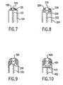
- FIG. 7shows another electrical contact embodiment.
- FIG. 8shows a further electrical contact embodiment.
- FIG. 9shows still another electrical contact embodiment.
- FIG. 10shows one more electrical contact embodiment.
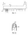
- FIG. 11is a schematic illustration of a single electrical contact such as that shown in FIG. 10 while in contact with a wafer surface during application of an electric field.
- FIG. 12shows part of another electrical contact embodiment which is similar to those of FIGS. 9 and 10 but in which a roller and a roller support member have different sizes.
- FIG. 2A general depiction of one version of a plating apparatus is shown in FIG. 2 .
- This apparatuscan also be used for plating and polishing as disclosed in commonly assigned application Ser. No. 09/201,929, filed Dec. 1, 1998, now U.S. Pat. No. 6,176,992, titled METHOD AND APPARATUS FOR ELECTROCHEMICAL MECHANICAL DEPOSITION, and commonly assigned application Ser. No. 09/472,523, filed Dec. 27, 1999, now U.S. Pat. No. 6,612,915, titled WORK PIECE CARRIER HEAD FOR PLATING AND POLISHING.
- the carrier head 10holds the wafer 16 .
- the waferhas the barrier layer and the seed layer (not shown in FIG.
- the headcan be rotated around a first axis 10 b . It can also be moved in the x, y, and z directions.
- a pad 8is placed on an anode plate 9 across from the wafer surface.
- the pad surfacemay itself be abrasive, or the pad may contain an abrasive material.
- Electrolyte 9 ais supplied to the wafer surface through the openings in the anode plate and the pad as shown by the arrows in FIG. 2 .
- Commonly assigned application Ser. No. 09/568,584, filed May 11, 2000, now U.S. Pat. No. 6,478,936, titled ANODE ASSEMBLY FOR PLATING AND PLANARIZING A CONDUCTIVE LAYERdiscloses an anode plate
- commonly assigned application Ser. No. 09/544,558filed Apr. 6, 2000, now U.S. Pat. No. 6,354,916, titled MODIFIED PLATING SOLUTION FOR PLATING AND PLANARIZATION, the disclosure of which is incorporated by reference herein as non-essential material, discloses an electrolyte.
- the electrolytethen flows over the edges of the pad into the chamber 9 c to be re-circulated after cleaning/filtering/refurbishing.
- An electrical contact 9 dis provided to the anode plate.
- the anode plateturns around the axis 10 c .
- the platemay also be translated in the x, y, and/or z directions.
- Axes 10 b and 10 care substantially parallel to each other.
- the diameter of the pad 8is typically smaller than the diameter of the wafer surface exposed to the pad surface, although it may also be larger.
- the gap between the wafer surface and the padis adjustable by moving the carrier head and/or the anode plate in the z direction.
- the workpiecei.e., the wafer or substrate
- the workpiecemay be brought close to the pad, without touching the pad.
- the workpiecehydroplanes or floats over the pad or anode.
- the wafer surface and the padmay be in contact. When the wafer surface and the pad are touching, the pressure that is exerted on the wafer and pad surfaces can also be adjusted.
- electrical connection to the wafer surfaceis made by way of multiple electrical contacts formed by pins that come up through the pad 8 and touch the wafer surface.
- FIG. 3A magnified view of one of the multiple electrical contacts is shown in FIG. 3 .
- Holes 24have been provided in the anode plate 9 to accommodate the pins 20 .
- These pins 20are electrically isolated from the anode plate 9 by an insulator 26 .
- the insulatormay be a ceramic or other appropriate dielectric material.
- a seal 25is interposed between the anode plate 9 and the insulator 26 .
- the pins 20 forming the electrical contactsare an integral part of a cathode plate 30 , which is also electrically isolated from the anode plate 9 by the insulator 26 .
- the cathode plate 30is spring loaded by suitable springs 32 which bias or push the rounded tips 20 T of the pins 20 towards the wafer surface 22 during the plating operation.
- the electrical contactscan slide up under the spring bias and down against the spring bias to adjust dynamically to the carrier head or workpiece location relative to the anode plate.
- a roller ballsimilar to that which could be used in a ball-point pen, can be incorporated at the tips 20 T to prevent scratching the wafer surface.
- Various additional or alternative electrical contact configurationswill be described in connection with FIGS. 7-12 .
- Soft conductive brushescan also be used to make contact to the wafer surface. It is important that the selected contacts do not scratch the wafer surface excessively.
- the electrolyte 9 ais supplied to the gap 34 between the pad 8 and the wafer surface 22 and thus is brought into physical contact with the wafer surface and the anode plate.
- the wafer 16is brought down until its surface 22 makes physical contact to the tips 20 T of the pins 20 .
- a potentialis applied between the cathode plate 30 and the anode plate 9 , making the cathode plate 30 more negative than the anode plate 9 . Therefore, the wafer surface is also rendered cathodic through the pins 20 . Under applied potential, copper plates out of the electrolyte 9 a onto the wafer surface 22 .
- the gap 34 between the pad 8 and the wafer surface 22 and/or by adjusting the pressure with which the pad 8 and the wafer surface 22 touch each otherone can achieve just plating, or plating and polishing.
- the pad 8have an abrasive surface or that the whole pad 8 is abrasive.
- the wafer or substrate 16 and the anode plate/pad assembly 8 , 9should rotate with respect to one another so that plating takes place uniformly. They may also translate in one or two directions.
- the electrolyte 9 atypically fills any gap 34 between the pad 8 and the wafer surface 22 . It is most preferable that the electrolyte 9 a be applied through channels in the anode plate 9 and the pad 8 (not shown in FIG. 3 ). Alternately, if the gap 34 is large (e.g. 2 mm or larger), the electrolyte can be provided into the gap 34 from the edges of the wafer.
- the pin tips 20 Tmay be disposed in close proximity to the wafer surface 22 without touching this surface.
- coppermay be either plated onto or removed from the wafer, depending on the polarity of the wafer. Circuitry used for application and adjustment of the applied potential, and for inverting the polarity of the potential, is well known and commonly used.
- the electrical contact to the wafer surfaceis made by way of a potential conductive pad 80 .
- This pad 80is used in place of the multiple pins 20 .
- an insulating spacer 82 of ceramic or other dielectric materialis placed directly over the anode plate 9 ′ between the anode plate 9 ′ and the conductive pad 80 .
- Electrical supply contactsare made to the conductive pad 80 and the anode plate 9 ′, and a cathodic potential is applied to the pad 80 , with electrolyte 9 a making physical contact to the anode plate 9 ′, the pad 80 and the wafer surface 22 .
- FIG. 4is similar to certain pad designs and structures forming the subject matter of application Ser. No. 09/511,278, filed Feb. 23, 2000, now U.S. Pat. No. 6,413,388, mentioned previously. Additionally, commonly assigned application Ser. No. 09/483,095, filed Jan. 14, 2000, now U.S. Pat. No. 6,630,059, titled SEMI CONDUCTOR WORKPIECE PROXIMITY PLATING METHODS AND APPARATUS, discloses conductive pad strips used on cylindrical anodes.
- the potential conductive pad 80may be allowed to float with respect to the wafer surface 22 during material deposition or removal.
- the potentialmoreover, may be pulsed to produce impulse plating.
- the circuitry used for pulsing the potentialis well known and commonly used.
- some Cu platingmay take place on the exposed cathodic surfaces besides the wafer surface.
- exposed regions of the pinsmay get coated.
- the whole padmay get coated. Therefore, it is of utmost importance to select the right conductive materials to be used for the construction of the electrical contacts and the pads.
- the materialsshould be such that plating on the Cu coated wafer surface (i.e. the seed layer 4 of FIG. 1 ) should be preferable or more efficient than plating on the pad or contact surface.
- Examples of proper materials for the padsmay be various conductive polymers or polymeric materials that are coated with refractory metals such as Ta, alpha Ta, W, Mo or their nitrides.
- the pins or other electrical contactscan be made of conductive polymers or refractory metals such as Mo, Ta and W; alternatively, the pins or other cathode contacts can be made of any conductive metal such as Cu or Ni, or of a conductive alloy such as Cu—Be, Cu—Ag, Ag—Pt, etc., but these metals or alloys may be coated by a refractory metal or compound and/or a nitride of a refractory metal, such as TaN or TiN, or of a refractory compound. These are just some examples. There are many more materials on which Cu does not deposit efficiently.
- the “edge exclusion” discussed earlier in connection with FIG. 1 acan be reduced on the wafer. As shown in FIG. 5 , eliminating the need for a contact ring to contact the periphery of the wafer permits a reduction of the edge exclusion “d”.
- the seal 18can be either on the surface 22 of the wafer 16 facing the electrolyte 9 a or right at the edge 16 a of the wafer. The seal 18 may even be disposed on the surface 35 of the wafer 16 facing away from the electrolyte 9 a.
- FIGS. 6 a - 6 cschematically show three possible types of distribution of pins 20 over a cathode plate 30 .
- the voltage drop from the center to the edge of the waferwill become smaller, and the thickness of the plated metal becomes more uniform.
- FIG. 7shows one of a plurality of electrical contacts which may be used as alternatives to, or together with, pins such as the pins 20 , or together with other electrical contact configurations, to provide the necessary electrical connection to a wafer surface.
- FIGS. 8-10 and 12also show additional electrical contact configurations which can be used as alternatives to, or together with, other contact configurations.
- Each electrical contact of FIG. 7includes a conductive roller 120 , which is preferably spherical in geometry. Rollers having other suitable geometrical shapes, such as cylindrical rollers, may be used. The rollers are preferably coated with a corrosion resistant material such as gold, platinum, pallidum, their alloys, or some other appropriate contact alloy material.
- the roller 120may be housed in an arrangement that may include, but is not limited to, a contact spring 122 to supply electrical power from the cathode plate (not shown) to the roller 120 .
- the end of the spring 122also acts as a bearing surface.
- the spring 122allows for a gentle but dynamic loading of the roller 120 on the surface of the workpiece.
- Each spring 122biases its respective roller toward the wafer surface.
- the electrical contact per seis formed by the roller 120 and the spring 122 which supports the roller.
- Each spring 122extends between the cathode plate (not shown in FIG. 7 ), on which the spring is supported in any appropriate fashion, and the roller 120 supported by the spring.
- Both the spring 122 and the roller 120are surrounded by an insulator 124 of a ceramic or other appropriate dielectric material that isolates the spring 122 and the roller 120 from an electric field during the process of plating Cu out of the electrolyte.
- the insulator 124may be configured similarly to the insulator 26 , represented in FIG. 1 , but can include a shaped tip 128 .
- the shaped tip 128 and a seal 126are disposed around the roller 120 .
- the seal 126may be adhesively or otherwise secured to the inner surface of the shaped tip.
- the seal arrangementis such that the roller 120 rotates freely with respect to the seal 126 .
- the electrolyte fluid boundary layerand, if the electrolyte forming the subject matter of copending application Ser. No. 09/544,558 mentioned above is used, especially the additive in the electrolyte, helps lubricate the roller surface.
- the tip 128In addition to housing the roller 120 and the seal 126 , the tip 128 also prevents the roller 120 from exposure to the electric field.
- FIG. 11which shows one electrical contact according to another embodiment in use, indicates an applied electric field by reference characters E. Consequently, the tip and seal configuration helps prevent or minimize material deposition on the roller 120 .
- FIG. 8shows another embodiment in which a rolling pad 230 of conducting material (e.g. metal), preferably with a partially spherical shaped surface, is disposed between the contact spring 222 and a spherical roller 220 .
- the roller 220rests on the shaped rolling pad 230 .
- the shaped tip 228 and the seal 226cooperate with the spring biased rolling pad 230 to confine the roller 220 while allowing it to rotate freely along any direction.
- the roller 220protrudes partly through but is restrained by the perimeter of an end opening in the insulator 224 which surrounds the seal 226 , the spring 222 , and the rolling pad 230 .
- the electrical contact per seis formed by the roller 220 , the spring 222 , and the spring biased rolling pad 230 disposed between the roller and the spring.
- FIG. 9shows that a conductive roller 320 may rest on a support member 330 having, for example, a spherical supporting surface rather than on a rolling pad. Multiple support members could be used beneath the roller 320 . Such an arrangement is ideal for self-aligned roller contact.
- the electrical contact per seis formed by the roller 320 , the spring 322 , and the support member 330 .
- the rolling fiction between the roller 320 and the substrate or workpieceis greatly reduced, especially when the workpiece rotates or translates during the process of plating Cu out of the electrolyte.
- the reduced frictionminimizes undesirable workpiece scratching and damage as well as particulate generation.
- a spherical support 430is disposed between a conductive roller pad 432 and the roller 420 .
- the electrical contact per seis formed by the roller 420 , the conductive spring 422 , the conductive spherical support 430 , and the spring biased and conductive rolling pad 432 .
- FIG. 11shows the embodiment of FIG. 10 in use during conductive material deposition.
- the size of the roller 520may be different from that of the roller support member 530 .
- roller materialthe contact spring material, and the like do not degrade or dissolve in the electrolyte of interest. It is also desirable that these materials do not degrade the quality of the material deposited.
- the rollerfor example, must not excessively scratch the deposited film or generate very undesirable particulates.
- Numerous face contactsmay be made around the periphery of the wafer. The individual contacts may be discrete and range from 4 to about 2000 in number, depending on size of the substrate. As the size of the wafer or substrate increases, the number of electrical contacts used should also increase.
- the roller contactscould also be a continuous race track or a track which is split into several elements. For example, the periphery may be divided into quadrants or octets. Each quadrant, etc., may contain many more or less uniformly dispersed roller contacts or contact tips.
Landscapes
- Chemical & Material Sciences (AREA)
- Engineering & Computer Science (AREA)
- Chemical Kinetics & Catalysis (AREA)
- Electrochemistry (AREA)
- Materials Engineering (AREA)
- Metallurgy (AREA)
- Organic Chemistry (AREA)
- Mechanical Engineering (AREA)
- Manufacturing & Machinery (AREA)
- Sustainable Development (AREA)
- Life Sciences & Earth Sciences (AREA)
- Condensed Matter Physics & Semiconductors (AREA)
- Microelectronics & Electronic Packaging (AREA)
- Power Engineering (AREA)
- Computer Hardware Design (AREA)
- General Physics & Mathematics (AREA)
- Physics & Mathematics (AREA)
- Electroplating Methods And Accessories (AREA)
- Electrodes Of Semiconductors (AREA)
Abstract
Description
Claims (34)
Priority Applications (2)
| Application Number | Priority Date | Filing Date | Title |
|---|---|---|---|
| US10/826,219US7311811B2 (en) | 2000-03-17 | 2004-04-16 | Device providing electrical contact to the surface of a semiconductor workpiece during processing |
| US11/123,268US7491308B2 (en) | 2000-03-17 | 2005-05-05 | Method of making rolling electrical contact to wafer front surface |
Applications Claiming Priority (7)
| Application Number | Priority Date | Filing Date | Title |
|---|---|---|---|
| US19002300P | 2000-03-17 | 2000-03-17 | |
| US09/685,934US6497800B1 (en) | 2000-03-17 | 2000-10-11 | Device providing electrical contact to the surface of a semiconductor workpiece during metal plating |
| US10/302,213US20030070930A1 (en) | 2000-03-17 | 2002-11-22 | Device providing electrical contact to the surface of a semiconductor workpiece during metal plating and method of providing such contact |
| US10/459,323US7329335B2 (en) | 2000-03-17 | 2003-06-10 | Device providing electrical contact to the surface of a semiconductor workpiece during processing |
| US10/459,321US7309413B2 (en) | 2000-03-17 | 2003-06-10 | Providing electrical contact to the surface of a semiconductor workpiece during processing |
| US10/459,320US7282124B2 (en) | 2000-03-17 | 2003-06-10 | Device providing electrical contact to the surface of a semiconductor workpiece during processing |
| US10/826,219US7311811B2 (en) | 2000-03-17 | 2004-04-16 | Device providing electrical contact to the surface of a semiconductor workpiece during processing |
Related Parent Applications (3)
| Application Number | Title | Priority Date | Filing Date |
|---|---|---|---|
| US10/459,321ContinuationUS7309413B2 (en) | 1998-12-01 | 2003-06-10 | Providing electrical contact to the surface of a semiconductor workpiece during processing |
| US10/459,320ContinuationUS7282124B2 (en) | 2000-03-17 | 2003-06-10 | Device providing electrical contact to the surface of a semiconductor workpiece during processing |
| US10/459,323ContinuationUS7329335B2 (en) | 2000-03-17 | 2003-06-10 | Device providing electrical contact to the surface of a semiconductor workpiece during processing |
Related Child Applications (1)
| Application Number | Title | Priority Date | Filing Date |
|---|---|---|---|
| US11/123,268ContinuationUS7491308B2 (en) | 2000-03-17 | 2005-05-05 | Method of making rolling electrical contact to wafer front surface |
Publications (2)
| Publication Number | Publication Date |
|---|---|
| US20040195111A1 US20040195111A1 (en) | 2004-10-07 |
| US7311811B2true US7311811B2 (en) | 2007-12-25 |
Family
ID=26885713
Family Applications (7)
| Application Number | Title | Priority Date | Filing Date |
|---|---|---|---|
| US09/685,934Expired - Fee RelatedUS6497800B1 (en) | 1998-12-01 | 2000-10-11 | Device providing electrical contact to the surface of a semiconductor workpiece during metal plating |
| US10/302,213AbandonedUS20030070930A1 (en) | 1998-12-01 | 2002-11-22 | Device providing electrical contact to the surface of a semiconductor workpiece during metal plating and method of providing such contact |
| US10/459,321Expired - LifetimeUS7309413B2 (en) | 1998-12-01 | 2003-06-10 | Providing electrical contact to the surface of a semiconductor workpiece during processing |
| US10/459,320Expired - Fee RelatedUS7282124B2 (en) | 2000-03-17 | 2003-06-10 | Device providing electrical contact to the surface of a semiconductor workpiece during processing |
| US10/459,323Expired - LifetimeUS7329335B2 (en) | 2000-03-17 | 2003-06-10 | Device providing electrical contact to the surface of a semiconductor workpiece during processing |
| US10/826,219Expired - LifetimeUS7311811B2 (en) | 2000-03-17 | 2004-04-16 | Device providing electrical contact to the surface of a semiconductor workpiece during processing |
| US11/123,268Expired - Fee RelatedUS7491308B2 (en) | 2000-03-17 | 2005-05-05 | Method of making rolling electrical contact to wafer front surface |
Family Applications Before (5)
| Application Number | Title | Priority Date | Filing Date |
|---|---|---|---|
| US09/685,934Expired - Fee RelatedUS6497800B1 (en) | 1998-12-01 | 2000-10-11 | Device providing electrical contact to the surface of a semiconductor workpiece during metal plating |
| US10/302,213AbandonedUS20030070930A1 (en) | 1998-12-01 | 2002-11-22 | Device providing electrical contact to the surface of a semiconductor workpiece during metal plating and method of providing such contact |
| US10/459,321Expired - LifetimeUS7309413B2 (en) | 1998-12-01 | 2003-06-10 | Providing electrical contact to the surface of a semiconductor workpiece during processing |
| US10/459,320Expired - Fee RelatedUS7282124B2 (en) | 2000-03-17 | 2003-06-10 | Device providing electrical contact to the surface of a semiconductor workpiece during processing |
| US10/459,323Expired - LifetimeUS7329335B2 (en) | 2000-03-17 | 2003-06-10 | Device providing electrical contact to the surface of a semiconductor workpiece during processing |
Family Applications After (1)
| Application Number | Title | Priority Date | Filing Date |
|---|---|---|---|
| US11/123,268Expired - Fee RelatedUS7491308B2 (en) | 2000-03-17 | 2005-05-05 | Method of making rolling electrical contact to wafer front surface |
Country Status (8)
| Country | Link |
|---|---|
| US (7) | US6497800B1 (en) |
| EP (1) | EP1268881A4 (en) |
| JP (1) | JP2003528219A (en) |
| KR (1) | KR100770464B1 (en) |
| CN (1) | CN1418264A (en) |
| AU (1) | AU2001238607A1 (en) |
| TW (1) | TW523783B (en) |
| WO (1) | WO2001071066A1 (en) |
Cited By (3)
| Publication number | Priority date | Publication date | Assignee | Title |
|---|---|---|---|---|
| US7947163B2 (en) | 2006-07-21 | 2011-05-24 | Novellus Systems, Inc. | Photoresist-free metal deposition |
| US8236160B2 (en) | 2000-08-10 | 2012-08-07 | Novellus Systems, Inc. | Plating methods for low aspect ratio cavities |
| US8268154B1 (en) | 2002-07-29 | 2012-09-18 | Novellus Systems, Inc. | Selective electrochemical accelerator removal |
Families Citing this family (107)
| Publication number | Priority date | Publication date | Assignee | Title |
|---|---|---|---|---|
| US7686935B2 (en)* | 1998-10-26 | 2010-03-30 | Novellus Systems, Inc. | Pad-assisted electropolishing |
| US6413388B1 (en)* | 2000-02-23 | 2002-07-02 | Nutool Inc. | Pad designs and structures for a versatile materials processing apparatus |
| US6497800B1 (en) | 2000-03-17 | 2002-12-24 | Nutool Inc. | Device providing electrical contact to the surface of a semiconductor workpiece during metal plating |
| US6902659B2 (en)* | 1998-12-01 | 2005-06-07 | Asm Nutool, Inc. | Method and apparatus for electro-chemical mechanical deposition |
| US6534116B2 (en)* | 2000-08-10 | 2003-03-18 | Nutool, Inc. | Plating method and apparatus that creates a differential between additive disposed on a top surface and a cavity surface of a workpiece using an external influence |
| US7427337B2 (en)* | 1998-12-01 | 2008-09-23 | Novellus Systems, Inc. | System for electropolishing and electrochemical mechanical polishing |
| US6251235B1 (en) | 1999-03-30 | 2001-06-26 | Nutool, Inc. | Apparatus for forming an electrical contact with a semiconductor substrate |
| US7578923B2 (en)* | 1998-12-01 | 2009-08-25 | Novellus Systems, Inc. | Electropolishing system and process |
| US6610190B2 (en)* | 2000-11-03 | 2003-08-26 | Nutool, Inc. | Method and apparatus for electrodeposition of uniform film with minimal edge exclusion on substrate |
| US6355153B1 (en)* | 1999-09-17 | 2002-03-12 | Nutool, Inc. | Chip interconnect and packaging deposition methods and structures |
| US6299741B1 (en)* | 1999-11-29 | 2001-10-09 | Applied Materials, Inc. | Advanced electrolytic polish (AEP) assisted metal wafer planarization method and apparatus |
| US6991526B2 (en) | 2002-09-16 | 2006-01-31 | Applied Materials, Inc. | Control of removal profile in electrochemically assisted CMP |
| US7303662B2 (en) | 2000-02-17 | 2007-12-04 | Applied Materials, Inc. | Contacts for electrochemical processing |
| US6979248B2 (en)* | 2002-05-07 | 2005-12-27 | Applied Materials, Inc. | Conductive polishing article for electrochemical mechanical polishing |
| US7374644B2 (en)* | 2000-02-17 | 2008-05-20 | Applied Materials, Inc. | Conductive polishing article for electrochemical mechanical polishing |
| US6962524B2 (en) | 2000-02-17 | 2005-11-08 | Applied Materials, Inc. | Conductive polishing article for electrochemical mechanical polishing |
| US7077721B2 (en) | 2000-02-17 | 2006-07-18 | Applied Materials, Inc. | Pad assembly for electrochemical mechanical processing |
| US7670468B2 (en) | 2000-02-17 | 2010-03-02 | Applied Materials, Inc. | Contact assembly and method for electrochemical mechanical processing |
| US6848970B2 (en) | 2002-09-16 | 2005-02-01 | Applied Materials, Inc. | Process control in electrochemically assisted planarization |
| US7029365B2 (en)* | 2000-02-17 | 2006-04-18 | Applied Materials Inc. | Pad assembly for electrochemical mechanical processing |
| US6884153B2 (en)* | 2000-02-17 | 2005-04-26 | Applied Materials, Inc. | Apparatus for electrochemical processing |
| US20030213703A1 (en)* | 2002-05-16 | 2003-11-20 | Applied Materials, Inc. | Method and apparatus for substrate polishing |
| US7066800B2 (en) | 2000-02-17 | 2006-06-27 | Applied Materials Inc. | Conductive polishing article for electrochemical mechanical polishing |
| US7303462B2 (en) | 2000-02-17 | 2007-12-04 | Applied Materials, Inc. | Edge bead removal by an electro polishing process |
| US7125477B2 (en) | 2000-02-17 | 2006-10-24 | Applied Materials, Inc. | Contacts for electrochemical processing |
| US7059948B2 (en) | 2000-12-22 | 2006-06-13 | Applied Materials | Articles for polishing semiconductor substrates |
| US7678245B2 (en) | 2000-02-17 | 2010-03-16 | Applied Materials, Inc. | Method and apparatus for electrochemical mechanical processing |
| US6991528B2 (en) | 2000-02-17 | 2006-01-31 | Applied Materials, Inc. | Conductive polishing article for electrochemical mechanical polishing |
| US6852208B2 (en)* | 2000-03-17 | 2005-02-08 | Nutool, Inc. | Method and apparatus for full surface electrotreating of a wafer |
| US20050284751A1 (en)* | 2004-06-28 | 2005-12-29 | Nicolay Kovarsky | Electrochemical plating cell with a counter electrode in an isolated anolyte compartment |
| US7754061B2 (en) | 2000-08-10 | 2010-07-13 | Novellus Systems, Inc. | Method for controlling conductor deposition on predetermined portions of a wafer |
| US20040170753A1 (en)* | 2000-12-18 | 2004-09-02 | Basol Bulent M. | Electrochemical mechanical processing using low temperature process environment |
| US6896776B2 (en) | 2000-12-18 | 2005-05-24 | Applied Materials Inc. | Method and apparatus for electro-chemical processing |
| US7172497B2 (en)* | 2001-01-05 | 2007-02-06 | Asm Nutool, Inc. | Fabrication of semiconductor interconnect structures |
| US7211174B2 (en)* | 2001-01-17 | 2007-05-01 | Novellus Systems, Inc. | Method and system to provide electrical contacts for electrotreating processes |
| US7244347B2 (en) | 2001-01-17 | 2007-07-17 | Novellus Systems, Inc. | Method and system to provide electrical contacts for electrotreating processes |
| US7211186B2 (en) | 2001-01-17 | 2007-05-01 | Novellus Systems, Inc. | Method and system to provide electrical contacts for electrotreating processes |
| US7344432B2 (en) | 2001-04-24 | 2008-03-18 | Applied Materials, Inc. | Conductive pad with ion exchange membrane for electrochemical mechanical polishing |
| US7137879B2 (en) | 2001-04-24 | 2006-11-21 | Applied Materials, Inc. | Conductive polishing article for electrochemical mechanical polishing |
| US6908540B2 (en)* | 2001-07-13 | 2005-06-21 | Applied Materials, Inc. | Method and apparatus for encapsulation of an edge of a substrate during an electro-chemical deposition process |
| US6863794B2 (en)* | 2001-09-21 | 2005-03-08 | Applied Materials, Inc. | Method and apparatus for forming metal layers |
| AU2002350038A1 (en)* | 2001-10-26 | 2003-05-06 | Nutool, Inc. | Method and system to provide electrical contacts for electrotreating processes |
| US6815354B2 (en)* | 2001-10-27 | 2004-11-09 | Nutool, Inc. | Method and structure for thru-mask contact electrodeposition |
| DE10162900C1 (en)* | 2001-12-20 | 2003-07-31 | Infineon Technologies Ag | Process for the production of low-resistance electrodes in trench capacitors |
| US6837983B2 (en)* | 2002-01-22 | 2005-01-04 | Applied Materials, Inc. | Endpoint detection for electro chemical mechanical polishing and electropolishing processes |
| US20030146102A1 (en)* | 2002-02-05 | 2003-08-07 | Applied Materials, Inc. | Method for forming copper interconnects |
| US20030168344A1 (en)* | 2002-03-08 | 2003-09-11 | Applied Materials, Inc. | Selective metal deposition for electrochemical plating |
| US6797144B2 (en)* | 2002-05-08 | 2004-09-28 | Taiwan Semiconductor Manufacturing Co., Ltd | Method for reducing surface defects in an electrodeposition process |
| TWI300026B (en)* | 2002-08-02 | 2008-08-21 | Applied Materials Inc | Conductive polishing article for electrochemical mechanical polishing |
| US7112270B2 (en) | 2002-09-16 | 2006-09-26 | Applied Materials, Inc. | Algorithm for real-time process control of electro-polishing |
| US20050061674A1 (en) | 2002-09-16 | 2005-03-24 | Yan Wang | Endpoint compensation in electroprocessing |
| US7025862B2 (en)* | 2002-10-22 | 2006-04-11 | Applied Materials | Plating uniformity control by contact ring shaping |
| US7138039B2 (en)* | 2003-01-21 | 2006-11-21 | Applied Materials, Inc. | Liquid isolation of contact rings |
| US7087144B2 (en)* | 2003-01-31 | 2006-08-08 | Applied Materials, Inc. | Contact ring with embedded flexible contacts |
| US7025861B2 (en)* | 2003-02-06 | 2006-04-11 | Applied Materials | Contact plating apparatus |
| US7842169B2 (en) | 2003-03-04 | 2010-11-30 | Applied Materials, Inc. | Method and apparatus for local polishing control |
| US6893328B2 (en)* | 2003-04-23 | 2005-05-17 | Rohm And Haas Electronic Materials Cmp Holdings, Inc. | Conductive polishing pad with anode and cathode |
| DK1620568T3 (en)* | 2003-04-24 | 2009-03-30 | Afshin Ahmadian | Analysis for allele-specific mutation detection |
| JP2004322292A (en)* | 2003-04-28 | 2004-11-18 | Yuzo Mori | Electrochemical machining device |
| WO2005002794A2 (en)* | 2003-07-01 | 2005-01-13 | Applied Materials, Inc. | Cell, system and article for electrochemical mechanical processing (ecmp) |
| US7345350B2 (en)* | 2003-09-23 | 2008-03-18 | Micron Technology, Inc. | Process and integration scheme for fabricating conductive components, through-vias and semiconductor components including conductive through-wafer vias |
| US8066552B2 (en) | 2003-10-03 | 2011-11-29 | Applied Materials, Inc. | Multi-layer polishing pad for low-pressure polishing |
| US20050173259A1 (en)* | 2004-02-06 | 2005-08-11 | Applied Materials, Inc. | Endpoint system for electro-chemical mechanical polishing |
| US7101792B2 (en)* | 2003-10-09 | 2006-09-05 | Micron Technology, Inc. | Methods of plating via interconnects |
| US7064057B2 (en)* | 2003-11-21 | 2006-06-20 | Asm Nutool, Inc. | Method and apparatus for localized material removal by electrochemical polishing |
| US7186164B2 (en) | 2003-12-03 | 2007-03-06 | Applied Materials, Inc. | Processing pad assembly with zone control |
| US20050121329A1 (en)* | 2003-12-05 | 2005-06-09 | Taiwan Semiconductor Manufacturing Co., Ltd. | Thrust pad assembly for ECP system |
| US7316063B2 (en)* | 2004-01-12 | 2008-01-08 | Micron Technology, Inc. | Methods of fabricating substrates including at least one conductive via |
| US7390744B2 (en) | 2004-01-29 | 2008-06-24 | Applied Materials, Inc. | Method and composition for polishing a substrate |
| US20050218000A1 (en)* | 2004-04-06 | 2005-10-06 | Applied Materials, Inc. | Conditioning of contact leads for metal plating systems |
| US7285195B2 (en) | 2004-06-24 | 2007-10-23 | Applied Materials, Inc. | Electric field reducing thrust plate |
| US7214297B2 (en)* | 2004-06-28 | 2007-05-08 | Applied Materials, Inc. | Substrate support element for an electrochemical plating cell |
| US7084064B2 (en) | 2004-09-14 | 2006-08-01 | Applied Materials, Inc. | Full sequence metal and barrier layer electrochemical mechanical processing |
| US20060183321A1 (en)* | 2004-09-27 | 2006-08-17 | Basol Bulent M | Method for reduction of gap fill defects |
| US7520968B2 (en) | 2004-10-05 | 2009-04-21 | Applied Materials, Inc. | Conductive pad design modification for better wafer-pad contact |
| JP2006135045A (en)* | 2004-11-05 | 2006-05-25 | Renesas Technology Corp | Polishing apparatus and method for manufacturing semiconductor device |
| US7655565B2 (en) | 2005-01-26 | 2010-02-02 | Applied Materials, Inc. | Electroprocessing profile control |
| US20060180465A1 (en)* | 2005-02-11 | 2006-08-17 | Applied Materials Inc. | Sliding flexible electrical contact for electrochemical processing |
| US7427340B2 (en) | 2005-04-08 | 2008-09-23 | Applied Materials, Inc. | Conductive pad |
| US20070056856A1 (en)* | 2005-09-13 | 2007-03-15 | Dongbuanam Semiconductor Inc. | Apparatus and method for electrically contacting wafer in electronic chemical plating cell |
| US7416975B2 (en) | 2005-09-21 | 2008-08-26 | Novellus Systems, Inc. | Method of forming contact layers on substrates |
| US20070096315A1 (en)* | 2005-11-01 | 2007-05-03 | Applied Materials, Inc. | Ball contact cover for copper loss reduction and spike reduction |
| US20070141818A1 (en)* | 2005-12-19 | 2007-06-21 | Bulent Basol | Method of depositing materials on full face of a wafer |
| US20070153453A1 (en)* | 2006-01-05 | 2007-07-05 | Applied Materials, Inc. | Fully conductive pad for electrochemical mechanical processing |
| US7550070B2 (en)* | 2006-02-03 | 2009-06-23 | Novellus Systems, Inc. | Electrode and pad assembly for processing conductive layers |
| EP1839695A1 (en)* | 2006-03-31 | 2007-10-03 | Debiotech S.A. | Medical liquid injection device |
| US20070235344A1 (en)* | 2006-04-06 | 2007-10-11 | Applied Materials, Inc. | Process for high copper removal rate with good planarization and surface finish |
| US20070251832A1 (en)* | 2006-04-27 | 2007-11-01 | Applied Materials, Inc. | Method and apparatus for electrochemical mechanical polishing of cu with higher liner velocity for better surface finish and higher removal rate during clearance |
| US7422982B2 (en) | 2006-07-07 | 2008-09-09 | Applied Materials, Inc. | Method and apparatus for electroprocessing a substrate with edge profile control |
| US7732329B2 (en)* | 2006-08-30 | 2010-06-08 | Ipgrip, Llc | Method and apparatus for workpiece surface modification for selective material deposition |
| DE102006043820A1 (en)* | 2006-09-19 | 2008-03-27 | Robert Bosch Gmbh | Device for processing a surface of a workpiece and method for producing a bipolar plate of a fuel cell by means of such a device |
| US20080237048A1 (en)* | 2007-03-30 | 2008-10-02 | Ismail Emesh | Method and apparatus for selective electrofilling of through-wafer vias |
| US8012000B2 (en)* | 2007-04-02 | 2011-09-06 | Applied Materials, Inc. | Extended pad life for ECMP and barrier removal |
| US8533821B2 (en) | 2007-05-25 | 2013-09-10 | International Business Machines Corporation | Detecting and defending against man-in-the-middle attacks |
| MD3970C2 (en)* | 2008-12-23 | 2010-05-31 | Институт Прикладной Физики Академии Наук Молдовы | Process for identification of the current-conducting object |
| US20100269162A1 (en) | 2009-04-15 | 2010-10-21 | Jose Bravo | Website authentication |
| US8683609B2 (en) | 2009-12-04 | 2014-03-25 | International Business Machines Corporation | Mobile phone and IP address correlation service |
| DE102012106053A1 (en)* | 2012-07-05 | 2014-01-09 | Doduco Gmbh | Electromechanical low-voltage switch |
| US8917826B2 (en) | 2012-07-31 | 2014-12-23 | International Business Machines Corporation | Detecting man-in-the-middle attacks in electronic transactions using prompts |
| US9222195B2 (en)* | 2012-09-05 | 2015-12-29 | Applied Materials, Inc. | Electroplating systems and methods for high sheet resistance substrates |
| JP6372329B2 (en)* | 2014-12-03 | 2018-08-15 | 富士通セミコンダクター株式会社 | Manufacturing method of semiconductor device |
| US10121708B2 (en)* | 2015-11-17 | 2018-11-06 | Lam Research Corporation | Systems and methods for detection of plasma instability by optical diagnosis |
| CN108368626B (en)* | 2015-12-03 | 2020-05-12 | 东京毅力科创株式会社 | Manufacturing apparatus and manufacturing method of semiconductor device |
| CN109790641B (en) | 2016-10-07 | 2021-10-22 | 东京毅力科创株式会社 | Electrolytic treatment jig and electrolytic treatment method |
| WO2019240891A1 (en) | 2018-06-15 | 2019-12-19 | Mattson Technology, Inc. | Methods and apparatus for post exposure bake processing of a workpiece |
| CN112458507A (en)* | 2020-10-26 | 2021-03-09 | 河南理工大学 | Electrodeposition writing system and method for preparing metal micro-nano structure in direct writing mode |
| KR20240079097A (en)* | 2022-11-28 | 2024-06-04 | (주)애니캐스팅 | S-ECAM printing apparatus for easy connection between substrate and power supply |
Citations (76)
| Publication number | Priority date | Publication date | Assignee | Title |
|---|---|---|---|---|
| US2540602A (en) | 1946-07-03 | 1951-02-06 | Lockheed Aircraft Corp | Method and apparatus for the surface treatment of metals |
| US2708181A (en) | 1951-05-17 | 1955-05-10 | Indiana Steel & Wire Company I | Electroplating process |
| US3328273A (en) | 1966-08-15 | 1967-06-27 | Udylite Corp | Electro-deposition of copper from acidic baths |
| US4339319A (en) | 1980-08-16 | 1982-07-13 | Seiichiro Aigo | Apparatus for plating semiconductor wafers |
| US4430173A (en) | 1981-07-24 | 1984-02-07 | Rhone-Poulenc Specialties Chimiques | Additive composition, bath and process for acid copper electroplating |
| US4713149A (en) | 1985-11-26 | 1987-12-15 | Shigeo Hoshino | Method and apparatus for electroplating objects |
| US4948474A (en) | 1987-09-18 | 1990-08-14 | Pennsylvania Research Corporation | Copper electroplating solutions and methods |
| US4954142A (en) | 1989-03-07 | 1990-09-04 | International Business Machines Corporation | Method of chemical-mechanical polishing an electronic component substrate and polishing slurry therefor |
| US4975159A (en) | 1988-10-24 | 1990-12-04 | Schering Aktiengesellschaft | Aqueous acidic bath for electrochemical deposition of a shiny and tear-free copper coating and method of using same |
| US5084071A (en) | 1989-03-07 | 1992-01-28 | International Business Machines Corporation | Method of chemical-mechanical polishing an electronic component substrate and polishing slurry therefor |
| US5256565A (en) | 1989-05-08 | 1993-10-26 | The United States Of America As Represented By The United States Department Of Energy | Electrochemical planarization |
| US5354490A (en) | 1992-06-04 | 1994-10-11 | Micron Technology, Inc. | Slurries for chemical mechanically polishing copper containing metal layers |
| US5466161A (en) | 1993-10-01 | 1995-11-14 | Bourns, Inc. | Compliant stacking connector for printed circuit boards |
| US5472592A (en) | 1994-07-19 | 1995-12-05 | American Plating Systems | Electrolytic plating apparatus and method |
| US5516412A (en) | 1995-05-16 | 1996-05-14 | International Business Machines Corporation | Vertical paddle plating cell |
| US5567300A (en) | 1994-09-02 | 1996-10-22 | Ibm Corporation | Electrochemical metal removal technique for planarization of surfaces |
| US5681215A (en) | 1995-10-27 | 1997-10-28 | Applied Materials, Inc. | Carrier head design for a chemical mechanical polishing apparatus |
| US5755859A (en) | 1995-08-24 | 1998-05-26 | International Business Machines Corporation | Cobalt-tin alloys and their applications for devices, chip interconnections and packaging |
| US5762544A (en) | 1995-10-27 | 1998-06-09 | Applied Materials, Inc. | Carrier head design for a chemical mechanical polishing apparatus |
| US5770095A (en) | 1994-07-12 | 1998-06-23 | Kabushiki Kaisha Toshiba | Polishing agent and polishing method using the same |
| WO1998027585A1 (en) | 1996-12-16 | 1998-06-25 | International Business Machines Corporation | Electroplated interconnection structures on integrated circuit chips |
| US5773364A (en) | 1996-10-21 | 1998-06-30 | Motorola, Inc. | Method for using ammonium salt slurries for chemical mechanical polishing (CMP) |
| US5793272A (en) | 1996-08-23 | 1998-08-11 | International Business Machines Corporation | Integrated circuit toroidal inductor |
| US5795215A (en) | 1995-06-09 | 1998-08-18 | Applied Materials, Inc. | Method and apparatus for using a retaining ring to control the edge effect |
| US5807165A (en) | 1997-03-26 | 1998-09-15 | International Business Machines Corporation | Method of electrochemical mechanical planarization |
| US5840629A (en) | 1995-12-14 | 1998-11-24 | Sematech, Inc. | Copper chemical mechanical polishing slurry utilizing a chromate oxidant |
| US5858813A (en) | 1996-05-10 | 1999-01-12 | Cabot Corporation | Chemical mechanical polishing slurry for metal layers and films |
| US5862605A (en) | 1996-05-24 | 1999-01-26 | Ebara Corporation | Vaporizer apparatus |
| US5897375A (en) | 1997-10-20 | 1999-04-27 | Motorola, Inc. | Chemical mechanical polishing (CMP) slurry for copper and method of use in integrated circuit manufacture |
| US5911619A (en) | 1997-03-26 | 1999-06-15 | International Business Machines Corporation | Apparatus for electrochemical mechanical planarization |
| US5922091A (en) | 1997-05-16 | 1999-07-13 | National Science Council Of Republic Of China | Chemical mechanical polishing slurry for metallic thin film |
| US5930669A (en) | 1997-04-03 | 1999-07-27 | International Business Machines Corporation | Continuous highly conductive metal wiring structures and method for fabricating the same |
| US5933753A (en) | 1996-12-16 | 1999-08-03 | International Business Machines Corporation | Open-bottomed via liner structure and method for fabricating same |
| US5954997A (en) | 1996-12-09 | 1999-09-21 | Cabot Corporation | Chemical mechanical polishing slurry useful for copper substrates |
| JPH11279797A (en) | 1998-03-27 | 1999-10-12 | Dainippon Screen Mfg Co Ltd | Substrate plating apparatus |
| US5985123A (en) | 1997-07-09 | 1999-11-16 | Koon; Kam Kwan | Continuous vertical plating system and method of plating |
| US6004880A (en) | 1998-02-20 | 1999-12-21 | Lsi Logic Corporation | Method of single step damascene process for deposition and global planarization |
| US6027631A (en) | 1997-11-13 | 2000-02-22 | Novellus Systems, Inc. | Electroplating system with shields for varying thickness profile of deposited layer |
| WO2000026443A2 (en) | 1998-11-03 | 2000-05-11 | Nutool, Inc. | Method and apparatus for electrochemical mechanical deposition |
| US6063506A (en) | 1995-06-27 | 2000-05-16 | International Business Machines Corporation | Copper alloys for chip and package interconnections |
| US6066030A (en) | 1999-03-04 | 2000-05-23 | International Business Machines Corporation | Electroetch and chemical mechanical polishing equipment |
| US6071388A (en) | 1998-05-29 | 2000-06-06 | International Business Machines Corporation | Electroplating workpiece fixture having liquid gap spacer |
| US6074544A (en) | 1998-07-22 | 2000-06-13 | Novellus Systems, Inc. | Method of electroplating semiconductor wafer using variable currents and mass transfer to obtain uniform plated layer |
| US6103085A (en) | 1998-12-04 | 2000-08-15 | Advanced Micro Devices, Inc. | Electroplating uniformity by diffuser design |
| US6106680A (en)* | 1999-01-26 | 2000-08-22 | Amd | Apparatus for forming a copper interconnect |
| US6132586A (en) | 1998-06-11 | 2000-10-17 | Integrated Process Equipment Corporation | Method and apparatus for non-contact metal plating of semiconductor wafers using a bipolar electrode assembly |
| US6132587A (en) | 1998-10-19 | 2000-10-17 | Jorne; Jacob | Uniform electroplating of wafers |
| US6136163A (en) | 1999-03-05 | 2000-10-24 | Applied Materials, Inc. | Apparatus for electro-chemical deposition with thermal anneal chamber |
| US6143155A (en) | 1998-06-11 | 2000-11-07 | Speedfam Ipec Corp. | Method for simultaneous non-contact electrochemical plating and planarizing of semiconductor wafers using a bipiolar electrode assembly |
| US6153064A (en) | 1998-11-25 | 2000-11-28 | Oliver Sales Company | Apparatus for in line plating |
| US6187152B1 (en) | 1998-07-17 | 2001-02-13 | Cutek Research, Inc. | Multiple station processing chamber and method for depositing and/or removing material on a substrate |
| US6228231B1 (en) | 1997-05-29 | 2001-05-08 | International Business Machines Corporation | Electroplating workpiece fixture having liquid gap spacer |
| US6251235B1 (en) | 1999-03-30 | 2001-06-26 | Nutool, Inc. | Apparatus for forming an electrical contact with a semiconductor substrate |
| US6251236B1 (en) | 1998-11-30 | 2001-06-26 | Applied Materials, Inc. | Cathode contact ring for electrochemical deposition |
| US6270646B1 (en) | 1999-12-28 | 2001-08-07 | International Business Machines Corporation | Electroplating apparatus and method using a compressible contact |
| US6299741B1 (en)* | 1999-11-29 | 2001-10-09 | Applied Materials, Inc. | Advanced electrolytic polish (AEP) assisted metal wafer planarization method and apparatus |
| US6334937B1 (en) | 1998-12-31 | 2002-01-01 | Semitool, Inc. | Apparatus for high deposition rate solder electroplating on a microelectronic workpiece |
| US6379223B1 (en) | 1999-11-29 | 2002-04-30 | Applied Materials, Inc. | Method and apparatus for electrochemical-mechanical planarization |
| US20020074238A1 (en) | 1998-10-26 | 2002-06-20 | Mayer Steven T. | Method and apparatus for uniform electropolishing of damascene ic structures by selective agitation |
| US20020102853A1 (en) | 2000-12-22 | 2002-08-01 | Applied Materials, Inc. | Articles for polishing semiconductor substrates |
| US6440295B1 (en) | 1998-07-09 | 2002-08-27 | Acm Research, Inc. | Method for electropolishing metal on semiconductor devices |
| US6482307B2 (en) | 2000-05-12 | 2002-11-19 | Nutool, Inc. | Method of and apparatus for making electrical contact to wafer surface for full-face electroplating or electropolishing |
| US6497800B1 (en) | 2000-03-17 | 2002-12-24 | Nutool Inc. | Device providing electrical contact to the surface of a semiconductor workpiece during metal plating |
| US6506103B1 (en) | 1999-07-23 | 2003-01-14 | Riken | ELID centerless grinding apparatus |
| US6534116B2 (en) | 2000-08-10 | 2003-03-18 | Nutool, Inc. | Plating method and apparatus that creates a differential between additive disposed on a top surface and a cavity surface of a workpiece using an external influence |
| US20030054729A1 (en) | 2000-08-30 | 2003-03-20 | Whonchee Lee | Methods and apparatus for electromechanically and/or electrochemically-mechanically removing conductive material from a microelectronic substrate |
| US6537144B1 (en) | 2000-02-17 | 2003-03-25 | Applied Materials, Inc. | Method and apparatus for enhanced CMP using metals having reductive properties |
| US6600229B2 (en) | 2001-01-23 | 2003-07-29 | Honeywell International Inc. | Planarizers for spin etch planarization of electronic components |
| US6610190B2 (en) | 2000-11-03 | 2003-08-26 | Nutool, Inc. | Method and apparatus for electrodeposition of uniform film with minimal edge exclusion on substrate |
| US6630059B1 (en) | 2000-01-14 | 2003-10-07 | Nutool, Inc. | Workpeice proximity plating apparatus |
| US6653226B1 (en) | 2001-01-09 | 2003-11-25 | Novellus Systems, Inc. | Method for electrochemical planarization of metal surfaces |
| US20030226764A1 (en) | 2000-08-30 | 2003-12-11 | Moore Scott E. | Methods and apparatus for electrochemical-mechanical processing of microelectronic workpieces |
| US20040178060A1 (en) | 2002-09-30 | 2004-09-16 | Lam Research Corp. | Apparatus and method for depositing and planarizing thin films of semiconductor wafers |
| US6848970B2 (en) | 2002-09-16 | 2005-02-01 | Applied Materials, Inc. | Process control in electrochemically assisted planarization |
| US6855239B1 (en) | 2002-09-27 | 2005-02-15 | Rahul Jairath | Plating method and apparatus using contactless electrode |
| US6902659B2 (en) | 1998-12-01 | 2005-06-07 | Asm Nutool, Inc. | Method and apparatus for electro-chemical mechanical deposition |
Family Cites Families (8)
| Publication number | Priority date | Publication date | Assignee | Title |
|---|---|---|---|---|
| US102853A (en)* | 1870-05-10 | Improved wheel for vehicles | ||
| US5135636A (en)* | 1990-10-12 | 1992-08-04 | Microelectronics And Computer Technology Corporation | Electroplating method |
| US5228231A (en)* | 1992-07-13 | 1993-07-20 | Hog Rustler, Inc. | Container for holding and dispensing fish bait or the like |
| US6395163B1 (en)* | 1992-08-01 | 2002-05-28 | Atotech Deutschland Gmbh | Process for the electrolytic processing especially of flat items and arrangement for implementing the process |
| US5930699A (en)* | 1996-11-12 | 1999-07-27 | Ericsson Inc. | Address retrieval system |
| CA2244314A1 (en)* | 1997-07-31 | 1999-01-31 | Sumitomo Chemical Co., Ltd. | Process for producing nucleoside derivatives |
| US5944955A (en) | 1998-01-15 | 1999-08-31 | Honeywell-Measurex Corporation | Fast basis weight control for papermaking machine |
| TW434735B (en)* | 1998-02-20 | 2001-05-16 | United Microelectronics Corp | Tungsten etcher installed with a bottom electrode bias power supply |
- 2000
- 2000-10-11USUS09/685,934patent/US6497800B1/ennot_activeExpired - Fee Related
- 2001
- 2001-02-22EPEP01911067Apatent/EP1268881A4/ennot_activeWithdrawn
- 2001-02-22WOPCT/US2001/005552patent/WO2001071066A1/enactiveApplication Filing
- 2001-02-22CNCN01806694Apatent/CN1418264A/enactivePending
- 2001-02-22KRKR1020027011983Apatent/KR100770464B1/ennot_activeExpired - Fee Related
- 2001-02-22JPJP2001569443Apatent/JP2003528219A/enactivePending
- 2001-02-22AUAU2001238607Apatent/AU2001238607A1/ennot_activeAbandoned
- 2001-03-12TWTW090105675Apatent/TW523783B/ennot_activeIP Right Cessation
- 2002
- 2002-11-22USUS10/302,213patent/US20030070930A1/ennot_activeAbandoned
- 2003
- 2003-06-10USUS10/459,321patent/US7309413B2/ennot_activeExpired - Lifetime
- 2003-06-10USUS10/459,320patent/US7282124B2/ennot_activeExpired - Fee Related
- 2003-06-10USUS10/459,323patent/US7329335B2/ennot_activeExpired - Lifetime
- 2004
- 2004-04-16USUS10/826,219patent/US7311811B2/ennot_activeExpired - Lifetime
- 2005
- 2005-05-05USUS11/123,268patent/US7491308B2/ennot_activeExpired - Fee Related
Patent Citations (83)
| Publication number | Priority date | Publication date | Assignee | Title |
|---|---|---|---|---|
| US2540602A (en) | 1946-07-03 | 1951-02-06 | Lockheed Aircraft Corp | Method and apparatus for the surface treatment of metals |
| US2708181A (en) | 1951-05-17 | 1955-05-10 | Indiana Steel & Wire Company I | Electroplating process |
| US3328273A (en) | 1966-08-15 | 1967-06-27 | Udylite Corp | Electro-deposition of copper from acidic baths |
| US4339319A (en) | 1980-08-16 | 1982-07-13 | Seiichiro Aigo | Apparatus for plating semiconductor wafers |
| US4430173A (en) | 1981-07-24 | 1984-02-07 | Rhone-Poulenc Specialties Chimiques | Additive composition, bath and process for acid copper electroplating |
| US4713149A (en) | 1985-11-26 | 1987-12-15 | Shigeo Hoshino | Method and apparatus for electroplating objects |
| US4948474A (en) | 1987-09-18 | 1990-08-14 | Pennsylvania Research Corporation | Copper electroplating solutions and methods |
| US4975159A (en) | 1988-10-24 | 1990-12-04 | Schering Aktiengesellschaft | Aqueous acidic bath for electrochemical deposition of a shiny and tear-free copper coating and method of using same |
| US5084071A (en) | 1989-03-07 | 1992-01-28 | International Business Machines Corporation | Method of chemical-mechanical polishing an electronic component substrate and polishing slurry therefor |
| US4954142A (en) | 1989-03-07 | 1990-09-04 | International Business Machines Corporation | Method of chemical-mechanical polishing an electronic component substrate and polishing slurry therefor |
| US5256565A (en) | 1989-05-08 | 1993-10-26 | The United States Of America As Represented By The United States Department Of Energy | Electrochemical planarization |
| US5354490A (en) | 1992-06-04 | 1994-10-11 | Micron Technology, Inc. | Slurries for chemical mechanically polishing copper containing metal layers |
| US5466161A (en) | 1993-10-01 | 1995-11-14 | Bourns, Inc. | Compliant stacking connector for printed circuit boards |
| US5770095A (en) | 1994-07-12 | 1998-06-23 | Kabushiki Kaisha Toshiba | Polishing agent and polishing method using the same |
| US5472592A (en) | 1994-07-19 | 1995-12-05 | American Plating Systems | Electrolytic plating apparatus and method |
| US5567300A (en) | 1994-09-02 | 1996-10-22 | Ibm Corporation | Electrochemical metal removal technique for planarization of surfaces |
| US5516412A (en) | 1995-05-16 | 1996-05-14 | International Business Machines Corporation | Vertical paddle plating cell |
| US5795215A (en) | 1995-06-09 | 1998-08-18 | Applied Materials, Inc. | Method and apparatus for using a retaining ring to control the edge effect |
| US6063506A (en) | 1995-06-27 | 2000-05-16 | International Business Machines Corporation | Copper alloys for chip and package interconnections |
| US5755859A (en) | 1995-08-24 | 1998-05-26 | International Business Machines Corporation | Cobalt-tin alloys and their applications for devices, chip interconnections and packaging |
| US5762544A (en) | 1995-10-27 | 1998-06-09 | Applied Materials, Inc. | Carrier head design for a chemical mechanical polishing apparatus |
| US5681215A (en) | 1995-10-27 | 1997-10-28 | Applied Materials, Inc. | Carrier head design for a chemical mechanical polishing apparatus |
| US5840629A (en) | 1995-12-14 | 1998-11-24 | Sematech, Inc. | Copper chemical mechanical polishing slurry utilizing a chromate oxidant |
| US5858813A (en) | 1996-05-10 | 1999-01-12 | Cabot Corporation | Chemical mechanical polishing slurry for metal layers and films |
| US5862605A (en) | 1996-05-24 | 1999-01-26 | Ebara Corporation | Vaporizer apparatus |
| US5793272A (en) | 1996-08-23 | 1998-08-11 | International Business Machines Corporation | Integrated circuit toroidal inductor |
| US5884990A (en) | 1996-08-23 | 1999-03-23 | International Business Machines Corporation | Integrated circuit inductor |
| US5773364A (en) | 1996-10-21 | 1998-06-30 | Motorola, Inc. | Method for using ammonium salt slurries for chemical mechanical polishing (CMP) |
| US5954997A (en) | 1996-12-09 | 1999-09-21 | Cabot Corporation | Chemical mechanical polishing slurry useful for copper substrates |
| WO1998027585A1 (en) | 1996-12-16 | 1998-06-25 | International Business Machines Corporation | Electroplated interconnection structures on integrated circuit chips |
| US5933753A (en) | 1996-12-16 | 1999-08-03 | International Business Machines Corporation | Open-bottomed via liner structure and method for fabricating same |
| US5807165A (en) | 1997-03-26 | 1998-09-15 | International Business Machines Corporation | Method of electrochemical mechanical planarization |
| US5911619A (en) | 1997-03-26 | 1999-06-15 | International Business Machines Corporation | Apparatus for electrochemical mechanical planarization |
| US5930669A (en) | 1997-04-03 | 1999-07-27 | International Business Machines Corporation | Continuous highly conductive metal wiring structures and method for fabricating the same |
| US5922091A (en) | 1997-05-16 | 1999-07-13 | National Science Council Of Republic Of China | Chemical mechanical polishing slurry for metallic thin film |
| US6228231B1 (en) | 1997-05-29 | 2001-05-08 | International Business Machines Corporation | Electroplating workpiece fixture having liquid gap spacer |
| US5985123A (en) | 1997-07-09 | 1999-11-16 | Koon; Kam Kwan | Continuous vertical plating system and method of plating |
| US5897375A (en) | 1997-10-20 | 1999-04-27 | Motorola, Inc. | Chemical mechanical polishing (CMP) slurry for copper and method of use in integrated circuit manufacture |
| US6027631A (en) | 1997-11-13 | 2000-02-22 | Novellus Systems, Inc. | Electroplating system with shields for varying thickness profile of deposited layer |
| US6004880A (en) | 1998-02-20 | 1999-12-21 | Lsi Logic Corporation | Method of single step damascene process for deposition and global planarization |
| JPH11279797A (en) | 1998-03-27 | 1999-10-12 | Dainippon Screen Mfg Co Ltd | Substrate plating apparatus |
| US6071388A (en) | 1998-05-29 | 2000-06-06 | International Business Machines Corporation | Electroplating workpiece fixture having liquid gap spacer |
| US6143155A (en) | 1998-06-11 | 2000-11-07 | Speedfam Ipec Corp. | Method for simultaneous non-contact electrochemical plating and planarizing of semiconductor wafers using a bipiolar electrode assembly |
| US6132586A (en) | 1998-06-11 | 2000-10-17 | Integrated Process Equipment Corporation | Method and apparatus for non-contact metal plating of semiconductor wafers using a bipolar electrode assembly |
| US6440295B1 (en) | 1998-07-09 | 2002-08-27 | Acm Research, Inc. | Method for electropolishing metal on semiconductor devices |
| US6187152B1 (en) | 1998-07-17 | 2001-02-13 | Cutek Research, Inc. | Multiple station processing chamber and method for depositing and/or removing material on a substrate |
| US6074544A (en) | 1998-07-22 | 2000-06-13 | Novellus Systems, Inc. | Method of electroplating semiconductor wafer using variable currents and mass transfer to obtain uniform plated layer |
| US6132587A (en) | 1998-10-19 | 2000-10-17 | Jorne; Jacob | Uniform electroplating of wafers |
| US20020074238A1 (en) | 1998-10-26 | 2002-06-20 | Mayer Steven T. | Method and apparatus for uniform electropolishing of damascene ic structures by selective agitation |
| WO2000026443A2 (en) | 1998-11-03 | 2000-05-11 | Nutool, Inc. | Method and apparatus for electrochemical mechanical deposition |
| US6402925B2 (en) | 1998-11-03 | 2002-06-11 | Nutool, Inc. | Method and apparatus for electrochemical mechanical deposition |
| US6176992B1 (en) | 1998-11-03 | 2001-01-23 | Nutool, Inc. | Method and apparatus for electro-chemical mechanical deposition |
| US6676822B1 (en) | 1998-11-03 | 2004-01-13 | Nutool, Inc. | Method for electro chemical mechanical deposition |
| US6153064A (en) | 1998-11-25 | 2000-11-28 | Oliver Sales Company | Apparatus for in line plating |
| US6251236B1 (en) | 1998-11-30 | 2001-06-26 | Applied Materials, Inc. | Cathode contact ring for electrochemical deposition |
| US6902659B2 (en) | 1998-12-01 | 2005-06-07 | Asm Nutool, Inc. | Method and apparatus for electro-chemical mechanical deposition |
| US6103085A (en) | 1998-12-04 | 2000-08-15 | Advanced Micro Devices, Inc. | Electroplating uniformity by diffuser design |
| US6334937B1 (en) | 1998-12-31 | 2002-01-01 | Semitool, Inc. | Apparatus for high deposition rate solder electroplating on a microelectronic workpiece |
| US6106680A (en)* | 1999-01-26 | 2000-08-22 | Amd | Apparatus for forming a copper interconnect |
| US6066030A (en) | 1999-03-04 | 2000-05-23 | International Business Machines Corporation | Electroetch and chemical mechanical polishing equipment |
| US6136163A (en) | 1999-03-05 | 2000-10-24 | Applied Materials, Inc. | Apparatus for electro-chemical deposition with thermal anneal chamber |
| US6251235B1 (en) | 1999-03-30 | 2001-06-26 | Nutool, Inc. | Apparatus for forming an electrical contact with a semiconductor substrate |
| US6958114B2 (en) | 1999-03-30 | 2005-10-25 | Asm Nutool, Inc. | Method and apparatus for forming an electrical contact with a semiconductor substrate |
| US6471847B2 (en) | 1999-03-30 | 2002-10-29 | Nutool, Inc. | Method for forming an electrical contact with a semiconductor substrate |
| US6506103B1 (en) | 1999-07-23 | 2003-01-14 | Riken | ELID centerless grinding apparatus |
| US6379223B1 (en) | 1999-11-29 | 2002-04-30 | Applied Materials, Inc. | Method and apparatus for electrochemical-mechanical planarization |
| US6299741B1 (en)* | 1999-11-29 | 2001-10-09 | Applied Materials, Inc. | Advanced electrolytic polish (AEP) assisted metal wafer planarization method and apparatus |
| US6270646B1 (en) | 1999-12-28 | 2001-08-07 | International Business Machines Corporation | Electroplating apparatus and method using a compressible contact |
| US6630059B1 (en) | 2000-01-14 | 2003-10-07 | Nutool, Inc. | Workpeice proximity plating apparatus |
| US6537144B1 (en) | 2000-02-17 | 2003-03-25 | Applied Materials, Inc. | Method and apparatus for enhanced CMP using metals having reductive properties |
| US6497800B1 (en) | 2000-03-17 | 2002-12-24 | Nutool Inc. | Device providing electrical contact to the surface of a semiconductor workpiece during metal plating |
| US6482307B2 (en) | 2000-05-12 | 2002-11-19 | Nutool, Inc. | Method of and apparatus for making electrical contact to wafer surface for full-face electroplating or electropolishing |
| US6534116B2 (en) | 2000-08-10 | 2003-03-18 | Nutool, Inc. | Plating method and apparatus that creates a differential between additive disposed on a top surface and a cavity surface of a workpiece using an external influence |
| US20030054729A1 (en) | 2000-08-30 | 2003-03-20 | Whonchee Lee | Methods and apparatus for electromechanically and/or electrochemically-mechanically removing conductive material from a microelectronic substrate |
| US20030226764A1 (en) | 2000-08-30 | 2003-12-11 | Moore Scott E. | Methods and apparatus for electrochemical-mechanical processing of microelectronic workpieces |
| US6610190B2 (en) | 2000-11-03 | 2003-08-26 | Nutool, Inc. | Method and apparatus for electrodeposition of uniform film with minimal edge exclusion on substrate |
| US6942780B2 (en) | 2000-11-03 | 2005-09-13 | Asm Nutool, Inc. | Method and apparatus for processing a substrate with minimal edge exclusion |
| US20020102853A1 (en) | 2000-12-22 | 2002-08-01 | Applied Materials, Inc. | Articles for polishing semiconductor substrates |
| US6653226B1 (en) | 2001-01-09 | 2003-11-25 | Novellus Systems, Inc. | Method for electrochemical planarization of metal surfaces |
| US6600229B2 (en) | 2001-01-23 | 2003-07-29 | Honeywell International Inc. | Planarizers for spin etch planarization of electronic components |
| US6848970B2 (en) | 2002-09-16 | 2005-02-01 | Applied Materials, Inc. | Process control in electrochemically assisted planarization |
| US6855239B1 (en) | 2002-09-27 | 2005-02-15 | Rahul Jairath | Plating method and apparatus using contactless electrode |
| US20040178060A1 (en) | 2002-09-30 | 2004-09-16 | Lam Research Corp. | Apparatus and method for depositing and planarizing thin films of semiconductor wafers |
Non-Patent Citations (11)
| Title |
|---|
| Co-Pending U.S. Appl. No. 10/123,268, filed May 5, 2005. |
| Co-Pending U.S. Appl. No. 10/302,213, filed Nov. 22, 2002. |
| Co-Pending U.S. Appl. No. 10/459,320, filed Jun. 10, 2003. |
| Co-Pending U.S. Appl. No. 10/459,321, filed Jun. 10, 2003. |
| Co-Pending U.S. Appl. No. 10/459,323, filed Jun. 10, 2003. |
| James J. Kelly et al., "Leveling and Microstructural Effects of Addictives for Copper Electrodeposition", Journal of Electrochemical Socirty, 146 (7), 1999, pp. 2540-2545. In related U.S. Appl. No. 09/685,934. |
| James J. Kelly et al., "Leveling and Microstructural Effects of Additives for Copper Electrodeposition", Journal of Electrochemical Society, 146 (7), 1999, pp. 2540-2545. |
| Joseph m. Steigerwald et al., "Chemical Mechanical Planarization of Microelectronic Materials", A Wiley-Interscience Publication, 1997 by John Wiley & Sons, Inc. pp. 212-222. |
| Joseph M. Steigerwald et al., "Chemical Mechanical Planarization of MicroelectronicMaterials", A Wiley-Interscience Publication, 1997 by John Wiley & Sons, Inc. pp. 212-222. In related U.S. Appl. No. 09/685,934. |
| Robert D. Mikkola et al., "Investigation of the Roles of the Additive Components for Secod Generation Copper Electroplating Chemistries Used for Advanced Interconnect Metalization", 2000 IEEE, IEEE Electron Devices Society, pp. 117-119, Jun. 2000. |
| Robert D. Mikkola et al., "Investigation of the Roles of the Additive Components for Second Generation Copper Electroplating Chemistries Used for Advanced Interconnect Metalization", 2000 IEEE, IEEE Electron Devices Society, pp. 117-119, Jun. 2000. In related U.S. Appl. No. 09/685,934. |
Cited By (5)
| Publication number | Priority date | Publication date | Assignee | Title |
|---|---|---|---|---|
| US8236160B2 (en) | 2000-08-10 | 2012-08-07 | Novellus Systems, Inc. | Plating methods for low aspect ratio cavities |
| US8268154B1 (en) | 2002-07-29 | 2012-09-18 | Novellus Systems, Inc. | Selective electrochemical accelerator removal |
| US8795482B1 (en) | 2002-07-29 | 2014-08-05 | Novellus Systems, Inc. | Selective electrochemical accelerator removal |
| US7947163B2 (en) | 2006-07-21 | 2011-05-24 | Novellus Systems, Inc. | Photoresist-free metal deposition |
| US8500985B2 (en) | 2006-07-21 | 2013-08-06 | Novellus Systems, Inc. | Photoresist-free metal deposition |
Also Published As
| Publication number | Publication date |
|---|---|
| US20050269212A1 (en) | 2005-12-08 |
| US20030209445A1 (en) | 2003-11-13 |
| CN1418264A (en) | 2003-05-14 |
| WO2001071066A1 (en) | 2001-09-27 |
| KR20020092382A (en) | 2002-12-11 |
| US7282124B2 (en) | 2007-10-16 |
| TW523783B (en) | 2003-03-11 |
| US20040195111A1 (en) | 2004-10-07 |
| EP1268881A1 (en) | 2003-01-02 |
| US20030217932A1 (en) | 2003-11-27 |
| US20030209425A1 (en) | 2003-11-13 |
| JP2003528219A (en) | 2003-09-24 |
| KR100770464B1 (en) | 2007-10-26 |
| US7491308B2 (en) | 2009-02-17 |
| US6497800B1 (en) | 2002-12-24 |
| US7329335B2 (en) | 2008-02-12 |
| AU2001238607A1 (en) | 2001-10-03 |
| US7309413B2 (en) | 2007-12-18 |
| US20030070930A1 (en) | 2003-04-17 |
| EP1268881A4 (en) | 2006-08-16 |
Similar Documents
| Publication | Publication Date | Title |
|---|---|---|
| US7311811B2 (en) | Device providing electrical contact to the surface of a semiconductor workpiece during processing | |
| US6482307B2 (en) | Method of and apparatus for making electrical contact to wafer surface for full-face electroplating or electropolishing | |
| US6176992B1 (en) | Method and apparatus for electro-chemical mechanical deposition | |
| US7341649B2 (en) | Apparatus for electroprocessing a workpiece surface | |
| US6837979B2 (en) | Method and apparatus for depositing and controlling the texture of a thin film | |
| US7572354B2 (en) | Electrochemical processing of conductive surface | |
| US6478936B1 (en) | Anode assembly for plating and planarizing a conductive layer | |
| US6852208B2 (en) | Method and apparatus for full surface electrotreating of a wafer | |
| US7211174B2 (en) | Method and system to provide electrical contacts for electrotreating processes | |
| US6863794B2 (en) | Method and apparatus for forming metal layers | |
| KR20050005389A (en) | Polishing Method and Polishing System, and Method for Fabricating Semiconductor Device | |
| US7244347B2 (en) | Method and system to provide electrical contacts for electrotreating processes | |
| US20050101138A1 (en) | System and method for applying constant pressure during electroplating and electropolishing | |
| KR20050009990A (en) | Polishing method, polishing device, and method of manufacturing semiconductor equipment | |
| JP2005509092A (en) | Electrochemical mechanical processing using an advanceable sweeper |
Legal Events
| Date | Code | Title | Description |
|---|---|---|---|
| AS | Assignment | Owner name:NUTOLL, INC., CALIFORNIA Free format text:ASSIGNMENT OF ASSIGNORS INTEREST;ASSIGNORS:TALIEH, HOMAYOUN;UZOH, CYPRIAN E.;BASOL, BULENT;REEL/FRAME:015231/0625 Effective date:20001005 | |
| AS | Assignment | Owner name:ASM NUTOOL, INC., CALIFORNIA Free format text:CHANGE OF NAME;ASSIGNOR:NUTOOL, INC.;REEL/FRAME:015479/0376 Effective date:20040729 | |
| AS | Assignment | Owner name:NOVELLUS SYSTEMS, INC.,CALIFORNIA Free format text:ASSIGNMENT OF ASSIGNORS INTEREST;ASSIGNOR:ASM NUTOOL, INC.;REEL/FRAME:019000/0080 Effective date:20061204 Owner name:NOVELLUS SYSTEMS, INC., CALIFORNIA Free format text:ASSIGNMENT OF ASSIGNORS INTEREST;ASSIGNOR:ASM NUTOOL, INC.;REEL/FRAME:019000/0080 Effective date:20061204 | |
| FEPP | Fee payment procedure | Free format text:PAYER NUMBER DE-ASSIGNED (ORIGINAL EVENT CODE: RMPN); ENTITY STATUS OF PATENT OWNER: LARGE ENTITY Free format text:PAYOR NUMBER ASSIGNED (ORIGINAL EVENT CODE: ASPN); ENTITY STATUS OF PATENT OWNER: LARGE ENTITY | |
| STCF | Information on status: patent grant | Free format text:PATENTED CASE | |
| FEPP | Fee payment procedure | Free format text:PAYER NUMBER DE-ASSIGNED (ORIGINAL EVENT CODE: RMPN); ENTITY STATUS OF PATENT OWNER: LARGE ENTITY Free format text:PAYOR NUMBER ASSIGNED (ORIGINAL EVENT CODE: ASPN); ENTITY STATUS OF PATENT OWNER: LARGE ENTITY | |
| CC | Certificate of correction | ||
| FPAY | Fee payment | Year of fee payment:4 | |
| FPAY | Fee payment | Year of fee payment:8 | |
| MAFP | Maintenance fee payment | Free format text:PAYMENT OF MAINTENANCE FEE, 12TH YEAR, LARGE ENTITY (ORIGINAL EVENT CODE: M1553); ENTITY STATUS OF PATENT OWNER: LARGE ENTITY Year of fee payment:12 |