US7310244B2 - Primary side controlled switching regulator - Google Patents
Primary side controlled switching regulatorDownload PDFInfo
- Publication number
- US7310244B2 US7310244B2US11/338,791US33879106AUS7310244B2US 7310244 B2US7310244 B2US 7310244B2US 33879106 AUS33879106 AUS 33879106AUS 7310244 B2US7310244 B2US 7310244B2
- Authority
- US
- United States
- Prior art keywords
- coupled
- signal
- transformer
- switch
- switching
- Prior art date
- Legal status (The legal status is an assumption and is not a legal conclusion. Google has not performed a legal analysis and makes no representation as to the accuracy of the status listed.)
- Active
Links
- 238000004804windingMethods0.000claimsabstractdescription131
- 239000003990capacitorSubstances0.000claimsabstractdescription48
- 230000001105regulatory effectEffects0.000claimsabstractdescription10
- 238000001514detection methodMethods0.000claimsdescription12
- 230000000737periodic effectEffects0.000claimsdescription8
- 238000010586diagramMethods0.000description12
- 230000003071parasitic effectEffects0.000description3
- 230000004907fluxEffects0.000description2
- 230000004048modificationEffects0.000description2
- 238000012986modificationMethods0.000description2
- 230000002596correlated effectEffects0.000description1
- 230000035699permeabilityEffects0.000description1
- 230000004044responseEffects0.000description1
Images
Classifications
- H—ELECTRICITY
- H02—GENERATION; CONVERSION OR DISTRIBUTION OF ELECTRIC POWER
- H02M—APPARATUS FOR CONVERSION BETWEEN AC AND AC, BETWEEN AC AND DC, OR BETWEEN DC AND DC, AND FOR USE WITH MAINS OR SIMILAR POWER SUPPLY SYSTEMS; CONVERSION OF DC OR AC INPUT POWER INTO SURGE OUTPUT POWER; CONTROL OR REGULATION THEREOF
- H02M1/00—Details of apparatus for conversion
- H02M1/44—Circuits or arrangements for compensating for electromagnetic interference in converters or inverters
- H—ELECTRICITY
- H02—GENERATION; CONVERSION OR DISTRIBUTION OF ELECTRIC POWER
- H02M—APPARATUS FOR CONVERSION BETWEEN AC AND AC, BETWEEN AC AND DC, OR BETWEEN DC AND DC, AND FOR USE WITH MAINS OR SIMILAR POWER SUPPLY SYSTEMS; CONVERSION OF DC OR AC INPUT POWER INTO SURGE OUTPUT POWER; CONTROL OR REGULATION THEREOF
- H02M3/00—Conversion of DC power input into DC power output
- H02M3/22—Conversion of DC power input into DC power output with intermediate conversion into AC
- H02M3/24—Conversion of DC power input into DC power output with intermediate conversion into AC by static converters
- H02M3/28—Conversion of DC power input into DC power output with intermediate conversion into AC by static converters using discharge tubes with control electrode or semiconductor devices with control electrode to produce the intermediate AC
- H02M3/325—Conversion of DC power input into DC power output with intermediate conversion into AC by static converters using discharge tubes with control electrode or semiconductor devices with control electrode to produce the intermediate AC using devices of a triode or a transistor type requiring continuous application of a control signal
- H02M3/335—Conversion of DC power input into DC power output with intermediate conversion into AC by static converters using discharge tubes with control electrode or semiconductor devices with control electrode to produce the intermediate AC using devices of a triode or a transistor type requiring continuous application of a control signal using semiconductor devices only
- H—ELECTRICITY
- H02—GENERATION; CONVERSION OR DISTRIBUTION OF ELECTRIC POWER
- H02M—APPARATUS FOR CONVERSION BETWEEN AC AND AC, BETWEEN AC AND DC, OR BETWEEN DC AND DC, AND FOR USE WITH MAINS OR SIMILAR POWER SUPPLY SYSTEMS; CONVERSION OF DC OR AC INPUT POWER INTO SURGE OUTPUT POWER; CONTROL OR REGULATION THEREOF
- H02M1/00—Details of apparatus for conversion
- H02M1/0003—Details of control, feedback or regulation circuits
- H02M1/0006—Arrangements for supplying an adequate voltage to the control circuit of converters
Definitions
- the present inventionrelates to a regulator, and more specifically relates to a switching regulator.
- a switching regulatortypically includes a control circuit, a switch and a transformer.
- the control circuitis applied to sense the output voltage and/or the output current of the switching regulator, and generate a control signal to control the switch and regulate the output voltage and/or the output current of the switching regulator.
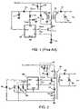
- FIG. 1shows a circuit diagram of a traditional switching regulator.
- the traditional switching regulatorincludes a transformer 10 having a primary winding N P , a secondary winding N S and an auxiliary winding N A .
- a terminal of the primary winding N Pis coupled to a positive supply rail V IN .
- a switch 11is connected from another terminal of the primary winding N P to a negative supply rail (a ground) through a resistor 12 .
- a control circuit 25is coupled to the switch 11 to control the switch 11 for switching the transformer 10 and regulating the output voltage and/or the output current of the switching regulator.
- a terminal of the secondary winding N Sconnects a rectifier 13 .
- a filter capacitor 14is coupled between the rectifier 13 and another terminal of the secondary winding N S .
- V O + V FN NS ⁇ d ⁇ d t ( 1 )
- V AUX ⁇ ⁇ 1N NA ⁇ d ⁇ d t ( 2 )
- the reflected voltage V AUX1can be expressed as
- V AUX ⁇ ⁇ 1N NA N NS ⁇ ( V O + V F ) ( 3 )
- N NA and N NSare respectively the winding turns of the auxiliary winding N A and the secondary winding N S of the transformer 10
- V Ois the output voltage of the switching regulator
- V Fis a forward voltage drop of the rectifier 13
- the control circuit 25comprises a supply terminal VDD and a ground terminal GND for receiving power.
- a voltage dividerincludes a resistor 15 and a resistor 16 connected between the auxiliary winding N A of the transformer 10 and the negative supply rail.
- a voltage detection terminal VS of the control circuit 25is connected to a joint of the resistor 15 and the resistor 16 .
- a detecting voltage V DET1 generated at the voltage detection terminal VSis given by,
- V DET ⁇ ⁇ 1R 16 R 15 + R 16 ⁇ V AUX ⁇ ⁇ 1 ( 4 ) where R 15 and R 16 are respectively the resistance of the resistors 15 and 16 .
- the reflected voltage V AUX1further charges a supplied capacitor 17 via a diode 18 to power the control circuit 25 .
- the resistor 12serves as a current sense device.
- the resistor 12is connected from the switch 11 to the negative supply rail for converting the transformer switching current I P into a current signal V CS .
- a current sense terminal VI of the control circuit 25is connected to the resistor 12 for detecting the current signal V CS .
- An output terminal VG of the control circuit 25generates the switching signal V PWM to switch the transformer 10 .
- This switching regulatoris generally used to regulate output voltage and output current, but it includes several disadvantages.
- One disadvantageis high power consumption caused by the leakage inductor of the transformer 10 .
- a snubber circuitincludes a snubber diode 19 , a snubber capacitor 20 and a snubber resistor 21 to consume the stored energy of the leakage inductor of the transformer 10 for protecting the switch 11 from a high voltage spike.
- Another disadvantage of this switching regulatoris a poor load regulation at light load and no load.
- the power of the control circuit 25is supplied from the auxiliary winding N A of the transformer 10 . Therefore, the operating current of the control circuit 25 represents the load of the auxiliary winding N A .
- the load at the output voltage V O of the switching regulatoris lower than the load consumed by the auxiliary winding N A , then the stored energy of the transformer 10 will only be discharged to the supplied capacitor 17 through the diode 18 and the auxiliary winding N A .
- the rectifier 13will remain off when the switch 11 is turned off. Therefore, the output voltage V O of the switching regulator cannot be feedback through the auxiliary winding N A .
- the detecting voltage V DET1 generated at the voltage detection terminal VSwill be only related to the voltage of the supply terminal VDD at light load and no load situations.
- the object of the present inventionis to provide a switching regulator having high efficiency and low EMI. Besides, the output voltage of the switching regulator can be accurately regulated at light load and no load.
- a switching regulatorincludes a transformer having a primary winding and an auxiliary winding.
- the primary windingis coupled to a positive supply rail.
- the auxiliary windingis coupled to a negative supply rail.
- a switchis connected in series with the primary winding and the auxiliary winding for switching the transformer.
- a current sense deviceis connected from the switch to the auxiliary winding for generating a current signal in accordance with a switching current of the transformer.
- a control circuitis coupled to the switch and the auxiliary winding of the transformer to generate a switching signal in response to the current signal. The switching signal is used for switching the switch and regulating the output of the switching regulator.
- a supplied capacitoris connected to the control circuit to supply the power to the control circuit.
- the auxiliary windinghas a leakage inductor to store a stored energy when the switch is on.
- a diodeis coupled from the negative supply rail to the supplied capacitor.
- the stored energy of the leakage inductoris discharged to the supplied capacitor through the diode once the switch is off.
- the connection of the transformer and the switchimproves the efficiency and reduces the EMI.
- FIG. 1shows a circuit diagram of a traditional switching regulator
- FIG. 2shows a circuit diagram of a primary-side controlled switching regulator according to one embodiment of the present invention
- FIG. 3shows an equivalent circuit diagram of the switching regulator shown in FIG. 2 ;
- FIG. 4shows a circuit diagram of a control circuit of the switching regulator according to one embodiment of the present invention
- FIG. 5shows a circuit diagram of another preferred embodiment of the switching regulator according to the present invention.
- FIG. 6shows a circuit diagram of another preferred embodiment of the switching regulator according to the present invention.
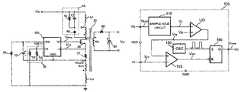
- FIG. 2shows a circuit diagram of a primary-side controlled switching regulator in accordance with the present invention.
- the switching regulatorincludes a transformer 30 for transferring a stored energy from a primary side of the transformer 30 to a secondary side of the transformer 30 .
- the primary side of the transformer 30has a primary winding N P and a first auxiliary winding N A1 .
- the secondary side of the transformer 30has a secondary winding N S .
- the primary winding N P and the first auxiliary winding N A1are coupled to the supply rail of the transformer 30 .
- the primary winding N Pis coupled to a positive supply rail V IN of the supply rail of the transformer 30 .
- the first auxiliary winding N A1is coupled to a negative supply rail (ground) of the supply rail of the transformer 30 .
- a switch 35is connected in series with the primary winding N P and the first auxiliary winding N A1 for switching the transformer 30 .
- the switch 35can be a power transistor or a power MOSFET. Because the switch 35 is connected in series with the primary winding N P and the first auxiliary winding N A1 , the high frequency resonant tank caused by the parasitic devices is eliminated and also the EMI is reduced.
- a current sense devicesuch as a current sense resistor 37 is connected from the switch 35 to the first auxiliary winding N A1 for generating a current signal V CS in accordance with the switching current I P of the transformer 30 .
- a control circuit 100is coupled to the switch 35 and the first auxiliary winding N A1 of the transformer 30 to generate a switching signal V PWM .
- the switching signal V PWMis used for switching the switch 35 and regulating the output voltage V O of the switching regulator.
- a supplied capacitor 70is connected to the control circuit 100 to supply the power to the control circuit 100 .
- a first diode 60is coupled between the supplied capacitor 70 and the negative supply rail of the transformer 30 .
- a snubber circuit 45is coupled between the primary winding N P and the positive supply rail V IN .
- the snubber circuit 45includes a snubber diode 40 , a snubber capacitor 41 and a snubber resistor 42 .
- a terminal of the snubber diode 40is coupled to the primary winding N P and the switch 35 .
- the snubber capacitor 41is coupled between another terminal of the snubber diode 40 and the positive supply rail V IN .
- the snubber resistor 42is coupled in parallel with the snubber capacitor 41 .
- a voltage divider 50is coupled between the first auxiliary winding N A1 and the negative supply rail.
- the voltage divider 50includes resistors 52 and 55 .
- the resistor 52is coupled between the control circuit 100 and the negative supply rail.
- the resistor 55is coupled between the resistor 52 and the first auxiliary winding N A1 .
- a rectifier 80is coupled to the secondary winding N S .
- a filter capacitor 90is coupled between the secondary winding N S and the rectifier 80 .
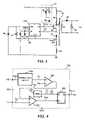
- FIG. 3shows an equivalent circuit diagram of the switching regulator shown in FIG. 2 .
- the primary winding N P and the first auxiliary winding N A1include leakage inductors L 11 and L 12 respectively. Due to the geometrical structure of the transformer, the stored energy of the primary side winding of the transformer cannot be fully transferred to other windings of the transformer.
- the leakage inductors L 11 and L 12stand for stored energy that cannot be transferred.
- the switching current I Pis flowed into the transformer 30 when the switch 35 is turned on. The energy is thus stored into the transformer 30 and leakage inductors L l1 and L l2 . When the switch 35 is turned off, the stored energy of the transformer 30 is discharged to the secondary winding N S . Meanwhile the stored energy of the leakage inductors L l1 and L l2 will be circulated within the loop. If the loop is locked, a voltage spike will be produced.
- VL ⁇ d i d t ( 5 )
- the snubber circuit 45is used to consume the stored energy of the leakage inductor L l1 for protecting the switch 35 from a high voltage spike.
- the power consumed by the snubber resistor 42 of the snubber circuit 45can be shown as,
- L⁇ ⁇ 0.4 ⁇ ⁇ ⁇ Ae li ⁇ N 2 ( 7 )
- Lis the inductance
- ⁇core permeability
- limagnetic path length
- Nis the number of winding turns
- Aeis the core cross-section of the transformer 30 .
- Connecting the primary winding N P in series with the first auxiliary winding N A1can reduce the winding turns so that the leakage inductance in the primary winding N P is reduced.
- the stored energy of the leakage inductor L l2is discharged to the supplied capacitor 70 through the first diode 60 once the switch 35 is off. Therefore, the stored energy of the leakage inductor L l2 is supplied to the control circuit 100 .
- the voltage V DD generated in the supplied capacitor 70can be shown as
- V DD[ N NA ⁇ ⁇ 1 N NS ⁇ ( V O + V F ) ] + V L ⁇ ⁇ 12 ( 8 )
- N NA1 and N NSare respectively the winding turns of the first auxiliary winding N A1 and the secondary winding N S of the transformer 30 .
- the V Ll2is the voltage generated by the leakage inductor L l2 . It is given by,
- the voltage V Ll2 generated by the leakage inductor L l2causes the voltage V DD on the supplied capacitor 70 is higher than the voltage reflected from the secondary winding N S of the transformer 30 .
- the rectifier 80is thus switched on once the switch 35 is switched off. Therefore, the output voltage V O of the switching regulator can be fed to the control circuit 100 through the first auxiliary winding N A1 .
- FIG. 4shows the circuit diagram of the control circuit 100 that includes a supply terminal VDD and a ground terminal GND parallel connected to the supplied capacitor 70 for receiving power.
- the supply terminal VDDis connected to the first diode 60 .
- the ground terminal GNDis connected to the first auxiliary winding N A1 .
- a voltage detection terminal VSis coupled to the first auxiliary winding N A1 through the voltage divider 50 for detecting a detecting voltage V DET2 from the first auxiliary winding N A1 of the transformer 30 .
- the detecting voltage V DET2can be expressed as,
- V DET ⁇ ⁇ 2R 52 R 52 + R 55 ( 11 ) where R 52 and R 55 are respectively the resistance of the resistors 52 and 55 ; V AUX2 is the voltage of the first auxiliary winding N A1 .
- a current sense terminal VIis coupled to the switch 35 and the current sense resistor 37 for receiving the current signal V CS .
- An output terminal VGis coupled to an output terminal of a flip-flip 160 to generate the switching signal V PWM for switching the transformer 30 via the switch 35 .
- An oscillator 150generates a periodic pulse signal transmitted to a set terminal of the flip-flop 160 . The periodic pulse signal is utilized to start the switching signal V PWM .
- a comparator 125is used to turn off the switching signal V PWM .
- a negative input terminal of the comparator 125is connected to the current sense terminal VI to receive the current signal V CS .
- a positive input terminal of the comparator 125is connected to an output terminal of an error amplifier 120 to receive a feedback signal V FB .
- the switching signal V PWMwill be turned off.
- An output terminal of the comparator 125is connected to a reset terminal of the flip-flip 160 to generate a reset signal V RST transmitted to the reset terminal to turn off the switching signal V PWM .
- the error amplifier 120is utilized to generate the feedback signal V FB .
- a positive input terminal of the error amplifier 120receives a reference voltage V R .
- a negative input terminal of the error amplifier 120is connected to an output terminal of a sample-hold circuit 110 to receive a sample signal V S .
- An input terminal of the sample-hold circuit 110is coupled to the voltage detection terminal VS to detect the detecting voltage V DET2 from the transformer 30 via the voltage divider 50 for generating the sample signal V S .
- the output voltage V O of the switching regulatoris therefore regulated.
- V O + V FN NS N NA ⁇ V AUX ⁇ ⁇ 2 ( 12 )
- V O( R 52 + R 55 R 52 ⁇ N NS N NA ⁇ V DET ⁇ ⁇ 2 ) - V F ( 13 )
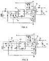
- FIG. 5shows a circuit diagram of another preferred embodiment of the switching regulator according to the present invention.
- the transformer 38includes the primary winding N P , the first auxiliary winding N A1 and a second auxiliary winding N A2 .
- the second auxiliary winding N A2 of the transformer 38is connected to the first auxiliary winding N A1 .
- the second auxiliary winding N A2is further connected to the supplied capacitor 70 through a second diode 65 .
- the ground terminal GNDis connected to the auxiliary windings N A1 and N A2 .
- the supply terminal VDDis connected to the supplied capacitor 70 , the first diode 60 and the second diode 65 .
- the first auxiliary winding N A1is used for providing the power to the control circuit 100 when the switch 35 is off, the voltage V DD generated on the supplied capacitor 70 is correlated to the output voltage V O of the switching regulator.
- the voltage V AUX2 of the first auxiliary winding N A1would be too low to supply power to the control circuit 100 if the output voltage V O of the switching regulator is under the overcurrent and/or short circuit circumstances.
- the second auxiliary winding N A2is thus developed to charge the supplied capacitor 70 when the switch 35 is switched on. Therefore, the second auxiliary winding N A2 provides a second source to supply power to the control circuit 100 , which ensures a proper operation of the control circuit 100 during the fault conditions.
- FIG. 6shows a circuit diagram of another preferred embodiment of the switching regulator according to the present invention.
- the transformer 39includes the primary winding N P , an inductor 32 and a third auxiliary winding N A3 .
- the inductor 32is connected in between the current sense resistor 37 and the negative supply rail.
- the third auxiliary winding N A3 of the transformer 39is connected to the supplied capacitor 70 through the second diode 65 .
- the third auxiliary winding N A3furthermore is coupled to the inductor 32 .
- a voltage divider 56 having a resistor 58 and a resistor 59is coupled between the third auxiliary winding N A3 and the inductor 32 .
- the resistor 58is coupled to the third auxiliary winding N A3 .
- the resistor 59is connected in series with the resistor 58 and the inductor 32 .
- the voltage detection terminal VS of the control circuit 100is coupled to the joint of the resistor 58 and the resistor 59 .
- the ground terminal GND of the control circuit 100is connected to the third auxiliary windings N A3 and the inductor 32 .
- the inductor 32is used for providing the power to the control circuit 100 through the first diode 60 when the switch 35 is turned off. Therefore, the power source of the control circuit 100 is provided from the third auxiliary winding N A3 and the inductor 32 , which will improve the load regulation at light load and no load conditions.
- the transformer windingsminimize the inductance of the leakage inductor.
- the stored energy of the leakage inductor of the auxiliary winding or inductoris used to provide power to the control circuit, which achieves better efficiency and improves the load regulation at light load and no load.
- the connection of the transformer and the switchresults a lower EMI.
Landscapes
- Engineering & Computer Science (AREA)
- Power Engineering (AREA)
- Physics & Mathematics (AREA)
- Electromagnetism (AREA)
- Dc-Dc Converters (AREA)
Abstract
Description
In accordance with equations (1) and (2), the reflected voltage VAUX1can be expressed as
where NNAand NNSare respectively the winding turns of the auxiliary winding NAand the secondary winding NSof the
where R15and R16are respectively the resistance of the
where R42is the resistance of the
where L is the inductance; μ is core permeability; li is magnetic path length; N is the number of winding turns; Ae is the core cross-section of the
where NNA1and NNSare respectively the winding turns of the first auxiliary winding NA1and the secondary winding NSof the
The VLl2is the voltage generated by the leakage inductor Ll2. It is given by,
where C70is the capacitance of the supplied
where R52and R55are respectively the resistance of the
Claims (11)
Priority Applications (1)
| Application Number | Priority Date | Filing Date | Title |
|---|---|---|---|
| US11/338,791US7310244B2 (en) | 2006-01-25 | 2006-01-25 | Primary side controlled switching regulator |
Applications Claiming Priority (1)
| Application Number | Priority Date | Filing Date | Title |
|---|---|---|---|
| US11/338,791US7310244B2 (en) | 2006-01-25 | 2006-01-25 | Primary side controlled switching regulator |
Publications (2)
| Publication Number | Publication Date |
|---|---|
| US20070171682A1 US20070171682A1 (en) | 2007-07-26 |
| US7310244B2true US7310244B2 (en) | 2007-12-18 |
Family
ID=38285357
Family Applications (1)
| Application Number | Title | Priority Date | Filing Date |
|---|---|---|---|
| US11/338,791ActiveUS7310244B2 (en) | 2006-01-25 | 2006-01-25 | Primary side controlled switching regulator |
Country Status (1)
| Country | Link |
|---|---|
| US (1) | US7310244B2 (en) |
Cited By (48)
| Publication number | Priority date | Publication date | Assignee | Title |
|---|---|---|---|---|
| US20080031018A1 (en)* | 2006-08-07 | 2008-02-07 | Linear Technology Corporation | Regulator for isolated flyback power supply using primary side sensing |
| US20080224636A1 (en)* | 2007-03-12 | 2008-09-18 | Melanson John L | Power control system for current regulated light sources |
| US20080240789A1 (en)* | 2007-03-28 | 2008-10-02 | Fuji Xerox Co., Ltd. | Rotator for powder conveyance and toner cartridge |
| US20080272747A1 (en)* | 2007-05-02 | 2008-11-06 | Cirrus Logic, Inc. | Programmable power control system |
| US20090189579A1 (en)* | 2008-01-30 | 2009-07-30 | Melanson John L | Switch state controller with a sense current generated operating voltage |
| US20090190384A1 (en)* | 2008-01-30 | 2009-07-30 | Cirrus Logic, Inc. | Powering a power supply integrated circuit with sense current |
| US20090191837A1 (en)* | 2008-01-30 | 2009-07-30 | Kartik Nanda | Delta Sigma Modulator with Unavailable Output Values |
| US20100148677A1 (en)* | 2008-12-12 | 2010-06-17 | Melanson John L | Time division light output sensing and brightness adjustment for different spectra of light emitting diodes |
| US20100164406A1 (en)* | 2008-07-25 | 2010-07-01 | Kost Michael A | Switching power converter control with triac-based leading edge dimmer compatibility |
| US20100164631A1 (en)* | 2008-12-31 | 2010-07-01 | Cirrus Logic, Inc. | Electronic system having common mode voltage range enhancement |
| US7759881B1 (en) | 2008-03-31 | 2010-07-20 | Cirrus Logic, Inc. | LED lighting system with a multiple mode current control dimming strategy |
| US7804697B2 (en) | 2007-12-11 | 2010-09-28 | Cirrus Logic, Inc. | History-independent noise-immune modulated transformer-coupled gate control signaling method and apparatus |
| US20100277072A1 (en)* | 2009-04-30 | 2010-11-04 | Draper William A | Calibration Of Lamps |
| US20100328976A1 (en)* | 2009-06-30 | 2010-12-30 | Melanson John L | Cascode configured switching using at least one low breakdown voltage internal, integrated circuit switch to control at least one high breakdown voltage external switch |
| US20110074302A1 (en)* | 2009-09-30 | 2011-03-31 | Draper William A | Phase Control Dimming Compatible Lighting Systems |
| US20110157923A1 (en)* | 2009-12-25 | 2011-06-30 | Ren Zhimou | Circuits and methods for controlling power converters including transformers |
| US20110156675A1 (en)* | 2009-12-28 | 2011-06-30 | Power Integrations, Inc. | Power converter having a switch coupled between windings |
| US20110156689A1 (en)* | 2009-12-28 | 2011-06-30 | Power Integrations, Inc. | Power converter having a switch coupled between windings |
| US8008902B2 (en) | 2008-06-25 | 2011-08-30 | Cirrus Logic, Inc. | Hysteretic buck converter having dynamic thresholds |
| US8008898B2 (en) | 2008-01-30 | 2011-08-30 | Cirrus Logic, Inc. | Switching regulator with boosted auxiliary winding supply |
| US8014176B2 (en) | 2008-07-25 | 2011-09-06 | Cirrus Logic, Inc. | Resonant switching power converter with burst mode transition shaping |
| US8018171B1 (en) | 2007-03-12 | 2011-09-13 | Cirrus Logic, Inc. | Multi-function duty cycle modifier |
| US20110227506A1 (en)* | 2010-02-25 | 2011-09-22 | O2Micro. Inc. | Controllers, systems and methods for controlling power of light sources |
| US8076920B1 (en) | 2007-03-12 | 2011-12-13 | Cirrus Logic, Inc. | Switching power converter and control system |
| US8102127B2 (en) | 2007-06-24 | 2012-01-24 | Cirrus Logic, Inc. | Hybrid gas discharge lamp-LED lighting system |
| US20120049831A1 (en)* | 2010-08-30 | 2012-03-01 | Chiu-Sing Celement Tse | Switching Converters |
| US8179110B2 (en) | 2008-09-30 | 2012-05-15 | Cirrus Logic Inc. | Adjustable constant current source with continuous conduction mode (“CCM”) and discontinuous conduction mode (“DCM”) operation |
| US8198874B2 (en) | 2009-06-30 | 2012-06-12 | Cirrus Logic, Inc. | Switching power converter with current sensing transformer auxiliary power supply |
| US8212493B2 (en) | 2009-06-30 | 2012-07-03 | Cirrus Logic, Inc. | Low energy transfer mode for auxiliary power supply operation in a cascaded switching power converter |
| US8222872B1 (en) | 2008-09-30 | 2012-07-17 | Cirrus Logic, Inc. | Switching power converter with selectable mode auxiliary power supply |
| US8288954B2 (en) | 2008-12-07 | 2012-10-16 | Cirrus Logic, Inc. | Primary-side based control of secondary-side current for a transformer |
| US8344707B2 (en) | 2008-07-25 | 2013-01-01 | Cirrus Logic, Inc. | Current sensing in a switching power converter |
| US8362707B2 (en) | 2008-12-12 | 2013-01-29 | Cirrus Logic, Inc. | Light emitting diode based lighting system with time division ambient light feedback response |
| US8487546B2 (en) | 2008-08-29 | 2013-07-16 | Cirrus Logic, Inc. | LED lighting system with accurate current control |
| US8536794B2 (en) | 2007-03-12 | 2013-09-17 | Cirrus Logic, Inc. | Lighting system with lighting dimmer output mapping |
| US8593075B1 (en) | 2011-06-30 | 2013-11-26 | Cirrus Logic, Inc. | Constant current controller with selectable gain |
| US8654483B2 (en) | 2009-11-09 | 2014-02-18 | Cirrus Logic, Inc. | Power system having voltage-based monitoring for over current protection |
| US8811045B2 (en) | 2009-12-25 | 2014-08-19 | 02Micro, Inc. | Circuits and methods for controlling power converters including transformers |
| US8912781B2 (en) | 2010-07-30 | 2014-12-16 | Cirrus Logic, Inc. | Integrated circuit switching power supply controller with selectable buck mode operation |
| US8963535B1 (en) | 2009-06-30 | 2015-02-24 | Cirrus Logic, Inc. | Switch controlled current sensing using a hall effect sensor |
| US9025347B2 (en) | 2010-12-16 | 2015-05-05 | Cirrus Logic, Inc. | Switching parameter based discontinuous mode-critical conduction mode transition |
| US20150204923A1 (en)* | 2014-01-17 | 2015-07-23 | Fairchild Korea Semiconductor Ltd. | Output current estimating method and power supply device using the same |
| US9166485B2 (en) | 2013-03-11 | 2015-10-20 | Cirrus Logic, Inc. | Quantization error reduction in constant output current control drivers |
| US9225252B2 (en) | 2013-03-11 | 2015-12-29 | Cirrus Logic, Inc. | Reduction of supply current variations using compensation current control |
| US9313840B2 (en) | 2011-06-03 | 2016-04-12 | Cirrus Logic, Inc. | Control data determination from primary-side sensing of a secondary-side voltage in a switching power converter |
| US9351356B2 (en) | 2011-06-03 | 2016-05-24 | Koninklijke Philips N.V. | Primary-side control of a switching power converter with feed forward delay compensation |
| US9941797B2 (en) | 2014-01-17 | 2018-04-10 | Semiconductor Components Industries, Llc | Switch control circuit and power supply device including the same |
| US20220393603A1 (en)* | 2021-06-08 | 2022-12-08 | Chengdu Monolithic Power Systems Co., Ltd. | Power supply circuit for switching mode power supply and control method thereof |
Families Citing this family (7)
| Publication number | Priority date | Publication date | Assignee | Title |
|---|---|---|---|---|
| MX2009000225A (en)* | 2006-06-26 | 2009-07-15 | Battelle Memorial Institute | High voltage power supply. |
| US7911808B2 (en)* | 2007-02-10 | 2011-03-22 | Active-Semi, Inc. | Primary side constant output current controller with highly improved accuracy |
| CN101398548B (en)* | 2007-09-28 | 2010-05-26 | 群康科技(深圳)有限公司 | Electric power circuit and LCD |
| JP2012161117A (en)* | 2011-01-28 | 2012-08-23 | Rohm Co Ltd | Dc/dc converter, and power supply device and electronic apparatus using the same |
| US8649194B2 (en)* | 2012-05-08 | 2014-02-11 | System General Corporation | Electro-magnetic interference reduction circuit for power converters and method thereof |
| JP6075827B2 (en)* | 2012-06-08 | 2017-02-08 | キヤノン株式会社 | Switching power supply device and image forming apparatus |
| CN103516236B (en)* | 2012-06-15 | 2016-05-25 | Tdk株式会社 | Converter |
Citations (6)
| Publication number | Priority date | Publication date | Assignee | Title |
|---|---|---|---|---|
| US4858052A (en)* | 1986-11-28 | 1989-08-15 | Ro Associates | Method and means for protecting converter circuits |
| US6917527B2 (en)* | 2003-01-23 | 2005-07-12 | Yokogawa Electric Corporation | Switching power supply |
| US20050162872A1 (en)* | 2004-01-26 | 2005-07-28 | Mitsumi Electric Co. Ltd. | DC/DC converter including a zener diode having a substantially zero temperature coefficient |
| US20050169017A1 (en)* | 2001-11-29 | 2005-08-04 | Muegge Mark R. | Methods for digital regulation of power converters using primary-only feedback |
| US7054170B2 (en)* | 2004-01-05 | 2006-05-30 | System General Corp. | Power-mode controlled power converter |
| US7123490B2 (en)* | 2004-08-11 | 2006-10-17 | Smk Corporation | Synchronous rectifying switching power source circuit |
- 2006
- 2006-01-25USUS11/338,791patent/US7310244B2/enactiveActive
Patent Citations (6)
| Publication number | Priority date | Publication date | Assignee | Title |
|---|---|---|---|---|
| US4858052A (en)* | 1986-11-28 | 1989-08-15 | Ro Associates | Method and means for protecting converter circuits |
| US20050169017A1 (en)* | 2001-11-29 | 2005-08-04 | Muegge Mark R. | Methods for digital regulation of power converters using primary-only feedback |
| US6917527B2 (en)* | 2003-01-23 | 2005-07-12 | Yokogawa Electric Corporation | Switching power supply |
| US7054170B2 (en)* | 2004-01-05 | 2006-05-30 | System General Corp. | Power-mode controlled power converter |
| US20050162872A1 (en)* | 2004-01-26 | 2005-07-28 | Mitsumi Electric Co. Ltd. | DC/DC converter including a zener diode having a substantially zero temperature coefficient |
| US7123490B2 (en)* | 2004-08-11 | 2006-10-17 | Smk Corporation | Synchronous rectifying switching power source circuit |
Cited By (80)
| Publication number | Priority date | Publication date | Assignee | Title |
|---|---|---|---|---|
| US7463497B2 (en)* | 2006-08-07 | 2008-12-09 | Linear Technology Corporation | Regulator for isolated flyback power supply using primary side sensing |
| US20080031018A1 (en)* | 2006-08-07 | 2008-02-07 | Linear Technology Corporation | Regulator for isolated flyback power supply using primary side sensing |
| US7804256B2 (en) | 2007-03-12 | 2010-09-28 | Cirrus Logic, Inc. | Power control system for current regulated light sources |
| US20080224636A1 (en)* | 2007-03-12 | 2008-09-18 | Melanson John L | Power control system for current regulated light sources |
| US8536794B2 (en) | 2007-03-12 | 2013-09-17 | Cirrus Logic, Inc. | Lighting system with lighting dimmer output mapping |
| US8174204B2 (en) | 2007-03-12 | 2012-05-08 | Cirrus Logic, Inc. | Lighting system with power factor correction control data determined from a phase modulated signal |
| US8076920B1 (en) | 2007-03-12 | 2011-12-13 | Cirrus Logic, Inc. | Switching power converter and control system |
| US8018171B1 (en) | 2007-03-12 | 2011-09-13 | Cirrus Logic, Inc. | Multi-function duty cycle modifier |
| US7852017B1 (en) | 2007-03-12 | 2010-12-14 | Cirrus Logic, Inc. | Ballast for light emitting diode light sources |
| US20080240789A1 (en)* | 2007-03-28 | 2008-10-02 | Fuji Xerox Co., Ltd. | Rotator for powder conveyance and toner cartridge |
| US8125805B1 (en) | 2007-05-02 | 2012-02-28 | Cirrus Logic Inc. | Switch-mode converter operating in a hybrid discontinuous conduction mode (DCM)/continuous conduction mode (CCM) that uses double or more pulses in a switching period |
| US7894216B2 (en) | 2007-05-02 | 2011-02-22 | Cirrus Logic, Inc. | Switching power converter with efficient switching control signal period generation |
| US20080273356A1 (en)* | 2007-05-02 | 2008-11-06 | Melanson John L | Switching Power Converter with Efficient Switching Control Signal Period Generation |
| US8120341B2 (en) | 2007-05-02 | 2012-02-21 | Cirrus Logic, Inc. | Switching power converter with switch control pulse width variability at low power demand levels |
| US7821237B2 (en) | 2007-05-02 | 2010-10-26 | Cirrus Logic, Inc. | Power factor correction (PFC) controller and method using a finite state machine to adjust the duty cycle of a PWM control signal |
| US8040703B2 (en) | 2007-05-02 | 2011-10-18 | Cirrus Logic, Inc. | Power factor correction controller with feedback reduction |
| US20080272747A1 (en)* | 2007-05-02 | 2008-11-06 | Cirrus Logic, Inc. | Programmable power control system |
| US7969125B2 (en) | 2007-05-02 | 2011-06-28 | Cirrus Logic, Inc. | Programmable power control system |
| US7863828B2 (en) | 2007-05-02 | 2011-01-04 | Cirrus Logic, Inc. | Power supply DC voltage offset detector |
| US7888922B2 (en) | 2007-05-02 | 2011-02-15 | Cirrus Logic, Inc. | Power factor correction controller with switch node feedback |
| US8102127B2 (en) | 2007-06-24 | 2012-01-24 | Cirrus Logic, Inc. | Hybrid gas discharge lamp-LED lighting system |
| US7804697B2 (en) | 2007-12-11 | 2010-09-28 | Cirrus Logic, Inc. | History-independent noise-immune modulated transformer-coupled gate control signaling method and apparatus |
| US8576589B2 (en) | 2008-01-30 | 2013-11-05 | Cirrus Logic, Inc. | Switch state controller with a sense current generated operating voltage |
| US8008898B2 (en) | 2008-01-30 | 2011-08-30 | Cirrus Logic, Inc. | Switching regulator with boosted auxiliary winding supply |
| US7755525B2 (en) | 2008-01-30 | 2010-07-13 | Cirrus Logic, Inc. | Delta sigma modulator with unavailable output values |
| US20090189579A1 (en)* | 2008-01-30 | 2009-07-30 | Melanson John L | Switch state controller with a sense current generated operating voltage |
| US20090190384A1 (en)* | 2008-01-30 | 2009-07-30 | Cirrus Logic, Inc. | Powering a power supply integrated circuit with sense current |
| US8022683B2 (en) | 2008-01-30 | 2011-09-20 | Cirrus Logic, Inc. | Powering a power supply integrated circuit with sense current |
| US20090191837A1 (en)* | 2008-01-30 | 2009-07-30 | Kartik Nanda | Delta Sigma Modulator with Unavailable Output Values |
| US7759881B1 (en) | 2008-03-31 | 2010-07-20 | Cirrus Logic, Inc. | LED lighting system with a multiple mode current control dimming strategy |
| US8008902B2 (en) | 2008-06-25 | 2011-08-30 | Cirrus Logic, Inc. | Hysteretic buck converter having dynamic thresholds |
| US8014176B2 (en) | 2008-07-25 | 2011-09-06 | Cirrus Logic, Inc. | Resonant switching power converter with burst mode transition shaping |
| US8344707B2 (en) | 2008-07-25 | 2013-01-01 | Cirrus Logic, Inc. | Current sensing in a switching power converter |
| US8212491B2 (en) | 2008-07-25 | 2012-07-03 | Cirrus Logic, Inc. | Switching power converter control with triac-based leading edge dimmer compatibility |
| US20100164406A1 (en)* | 2008-07-25 | 2010-07-01 | Kost Michael A | Switching power converter control with triac-based leading edge dimmer compatibility |
| US8553430B2 (en) | 2008-07-25 | 2013-10-08 | Cirrus Logic, Inc. | Resonant switching power converter with adaptive dead time control |
| US8279628B2 (en) | 2008-07-25 | 2012-10-02 | Cirrus Logic, Inc. | Audible noise suppression in a resonant switching power converter |
| US8487546B2 (en) | 2008-08-29 | 2013-07-16 | Cirrus Logic, Inc. | LED lighting system with accurate current control |
| US8179110B2 (en) | 2008-09-30 | 2012-05-15 | Cirrus Logic Inc. | Adjustable constant current source with continuous conduction mode (“CCM”) and discontinuous conduction mode (“DCM”) operation |
| US8222872B1 (en) | 2008-09-30 | 2012-07-17 | Cirrus Logic, Inc. | Switching power converter with selectable mode auxiliary power supply |
| US8581505B2 (en) | 2008-12-07 | 2013-11-12 | Cirrus Logic, Inc. | Primary-side based control of secondary-side current for a transformer |
| US8288954B2 (en) | 2008-12-07 | 2012-10-16 | Cirrus Logic, Inc. | Primary-side based control of secondary-side current for a transformer |
| US8362707B2 (en) | 2008-12-12 | 2013-01-29 | Cirrus Logic, Inc. | Light emitting diode based lighting system with time division ambient light feedback response |
| US20100148677A1 (en)* | 2008-12-12 | 2010-06-17 | Melanson John L | Time division light output sensing and brightness adjustment for different spectra of light emitting diodes |
| US8299722B2 (en) | 2008-12-12 | 2012-10-30 | Cirrus Logic, Inc. | Time division light output sensing and brightness adjustment for different spectra of light emitting diodes |
| US7994863B2 (en) | 2008-12-31 | 2011-08-09 | Cirrus Logic, Inc. | Electronic system having common mode voltage range enhancement |
| US20100164631A1 (en)* | 2008-12-31 | 2010-07-01 | Cirrus Logic, Inc. | Electronic system having common mode voltage range enhancement |
| US8482223B2 (en) | 2009-04-30 | 2013-07-09 | Cirrus Logic, Inc. | Calibration of lamps |
| US20100277072A1 (en)* | 2009-04-30 | 2010-11-04 | Draper William A | Calibration Of Lamps |
| US8963535B1 (en) | 2009-06-30 | 2015-02-24 | Cirrus Logic, Inc. | Switch controlled current sensing using a hall effect sensor |
| US8248145B2 (en) | 2009-06-30 | 2012-08-21 | Cirrus Logic, Inc. | Cascode configured switching using at least one low breakdown voltage internal, integrated circuit switch to control at least one high breakdown voltage external switch |
| US8198874B2 (en) | 2009-06-30 | 2012-06-12 | Cirrus Logic, Inc. | Switching power converter with current sensing transformer auxiliary power supply |
| US8212493B2 (en) | 2009-06-30 | 2012-07-03 | Cirrus Logic, Inc. | Low energy transfer mode for auxiliary power supply operation in a cascaded switching power converter |
| US20100328976A1 (en)* | 2009-06-30 | 2010-12-30 | Melanson John L | Cascode configured switching using at least one low breakdown voltage internal, integrated circuit switch to control at least one high breakdown voltage external switch |
| US20110074302A1 (en)* | 2009-09-30 | 2011-03-31 | Draper William A | Phase Control Dimming Compatible Lighting Systems |
| US9155174B2 (en) | 2009-09-30 | 2015-10-06 | Cirrus Logic, Inc. | Phase control dimming compatible lighting systems |
| US8654483B2 (en) | 2009-11-09 | 2014-02-18 | Cirrus Logic, Inc. | Power system having voltage-based monitoring for over current protection |
| US20110157923A1 (en)* | 2009-12-25 | 2011-06-30 | Ren Zhimou | Circuits and methods for controlling power converters including transformers |
| US8811045B2 (en) | 2009-12-25 | 2014-08-19 | 02Micro, Inc. | Circuits and methods for controlling power converters including transformers |
| US8379413B2 (en) | 2009-12-25 | 2013-02-19 | 02Micro Inc. | Circuits and methods for controlling power converters including transformers |
| US8558484B2 (en)* | 2009-12-28 | 2013-10-15 | Power Integrations, Inc. | Power converter having a switch coupled between windings |
| US20110156689A1 (en)* | 2009-12-28 | 2011-06-30 | Power Integrations, Inc. | Power converter having a switch coupled between windings |
| US8933649B2 (en) | 2009-12-28 | 2015-01-13 | Power Integrations, Inc. | Power converter having a switch coupled between windings |
| US20110156675A1 (en)* | 2009-12-28 | 2011-06-30 | Power Integrations, Inc. | Power converter having a switch coupled between windings |
| US20110227506A1 (en)* | 2010-02-25 | 2011-09-22 | O2Micro. Inc. | Controllers, systems and methods for controlling power of light sources |
| US8233292B2 (en)* | 2010-02-25 | 2012-07-31 | O2Micro, Inc. | Controllers, systems and methods for controlling power of light sources |
| US8912781B2 (en) | 2010-07-30 | 2014-12-16 | Cirrus Logic, Inc. | Integrated circuit switching power supply controller with selectable buck mode operation |
| US20120049831A1 (en)* | 2010-08-30 | 2012-03-01 | Chiu-Sing Celement Tse | Switching Converters |
| US8804385B2 (en)* | 2010-08-30 | 2014-08-12 | Mosway Semiconductor Limited | SMPS control IC with 4 terminals |
| US9025347B2 (en) | 2010-12-16 | 2015-05-05 | Cirrus Logic, Inc. | Switching parameter based discontinuous mode-critical conduction mode transition |
| US9313840B2 (en) | 2011-06-03 | 2016-04-12 | Cirrus Logic, Inc. | Control data determination from primary-side sensing of a secondary-side voltage in a switching power converter |
| US9351356B2 (en) | 2011-06-03 | 2016-05-24 | Koninklijke Philips N.V. | Primary-side control of a switching power converter with feed forward delay compensation |
| US8593075B1 (en) | 2011-06-30 | 2013-11-26 | Cirrus Logic, Inc. | Constant current controller with selectable gain |
| US9225252B2 (en) | 2013-03-11 | 2015-12-29 | Cirrus Logic, Inc. | Reduction of supply current variations using compensation current control |
| US9166485B2 (en) | 2013-03-11 | 2015-10-20 | Cirrus Logic, Inc. | Quantization error reduction in constant output current control drivers |
| US20150204923A1 (en)* | 2014-01-17 | 2015-07-23 | Fairchild Korea Semiconductor Ltd. | Output current estimating method and power supply device using the same |
| US9825541B2 (en)* | 2014-01-17 | 2017-11-21 | Fairchild Korea Semiconductor Ltd. | Output current estimating method and power supply device using the same |
| US9941797B2 (en) | 2014-01-17 | 2018-04-10 | Semiconductor Components Industries, Llc | Switch control circuit and power supply device including the same |
| US20220393603A1 (en)* | 2021-06-08 | 2022-12-08 | Chengdu Monolithic Power Systems Co., Ltd. | Power supply circuit for switching mode power supply and control method thereof |
| US11716029B2 (en)* | 2021-06-08 | 2023-08-01 | Chengdu Monolithic Power Systems Co., Ltd. | Power supply circuit for switching mode power supply and control method thereof |
Also Published As
| Publication number | Publication date |
|---|---|
| US20070171682A1 (en) | 2007-07-26 |
Similar Documents
| Publication | Publication Date | Title |
|---|---|---|
| US7310244B2 (en) | Primary side controlled switching regulator | |
| US20070159856A1 (en) | Flyback power converter with split primary winding transformer | |
| US20070159143A1 (en) | Switching power converter with transformer arrangement | |
| US6788556B2 (en) | Switching power source device | |
| US6061252A (en) | Switching power supply device | |
| US7672146B2 (en) | Switching mode power supply and driving method | |
| US9287792B2 (en) | Control method to reduce switching loss on MOSFET | |
| US7426120B2 (en) | Switching control circuit having a valley voltage detector to achieve soft switching for a resonant power converter | |
| JP3475887B2 (en) | Switching power supply | |
| US6714428B2 (en) | Combined transformer-inductor device for application to DC-to-DC converter with synchronous rectifier | |
| US8009448B2 (en) | Forward-flyback converter with active-clamp circuit | |
| US7577003B2 (en) | Switching power supply | |
| EP0765022B1 (en) | Uninterrupted switching regulator | |
| JPH09163736A (en) | Dc-dc converter | |
| JPWO2007046195A1 (en) | Synchronous rectification forward converter | |
| CN114568041A (en) | Flyback converter and operation method thereof | |
| US7656691B2 (en) | Charge mode control of a serial resonance converter | |
| JP2004153948A (en) | Switching power transmission equipment | |
| US7057906B2 (en) | Insulating switching DC/DC converter | |
| US20060007711A1 (en) | Half-bridge flyback power converter | |
| US12273028B2 (en) | Resonant AHB flyback power converter and switching control circuit thereof | |
| US12126268B2 (en) | Synchronous rectifiers and charging methods used therein | |
| KR100387381B1 (en) | Switching mode power supply with high efficiency | |
| US11632051B2 (en) | Flyback converter and method of operating the same | |
| JP2002305876A (en) | Switching power supply |
Legal Events
| Date | Code | Title | Description |
|---|---|---|---|
| AS | Assignment | Owner name:SYSTEM GENERAL CORP., TAIWAN Free format text:ASSIGNMENT OF ASSIGNORS INTEREST;ASSIGNORS:YANG, TA-YUNG;CHENG, PEI-HSUAN;REEL/FRAME:017232/0068 Effective date:20060105 | |
| STCF | Information on status: patent grant | Free format text:PATENTED CASE | |
| FPAY | Fee payment | Year of fee payment:4 | |
| FPAY | Fee payment | Year of fee payment:8 | |
| AS | Assignment | Owner name:FAIRCHILD (TAIWAN) CORPORATION, TAIWAN Free format text:CHANGE OF NAME;ASSIGNOR:SYSTEM GENERAL CORP.;REEL/FRAME:038906/0030 Effective date:20140620 | |
| AS | Assignment | Owner name:SEMICONDUCTOR COMPONENTS INDUSTRIES, LLC, ARIZONA Free format text:ASSIGNMENT OF ASSIGNORS INTEREST;ASSIGNOR:FAIRCHILD (TAIWAN) CORPORATION (FORMERLY SYSTEM GENERAL CORPORATION);REEL/FRAME:042328/0318 Effective date:20161221 | |
| AS | Assignment | Owner name:DEUTSCHE BANK AG NEW YORK BRANCH, AS COLLATERAL AGENT, NEW YORK Free format text:PATENT SECURITY AGREEMENT;ASSIGNOR:SEMICONDUCTOR COMPONENTS INDUSTRIES, LLC;REEL/FRAME:046410/0933 Effective date:20170210 Owner name:DEUTSCHE BANK AG NEW YORK BRANCH, AS COLLATERAL AG Free format text:PATENT SECURITY AGREEMENT;ASSIGNOR:SEMICONDUCTOR COMPONENTS INDUSTRIES, LLC;REEL/FRAME:046410/0933 Effective date:20170210 | |
| MAFP | Maintenance fee payment | Free format text:PAYMENT OF MAINTENANCE FEE, 12TH YEAR, LARGE ENTITY (ORIGINAL EVENT CODE: M1553); ENTITY STATUS OF PATENT OWNER: LARGE ENTITY Year of fee payment:12 | |
| AS | Assignment | Owner name:FAIRCHILD SEMICONDUCTOR CORPORATION, ARIZONA Free format text:RELEASE OF SECURITY INTEREST IN PATENTS RECORDED AT RECORDED AT REEL 046410, FRAME 0933;ASSIGNOR:DEUTSCHE BANK AG NEW YORK BRANCH, AS COLLATERAL AGENT;REEL/FRAME:064072/0001 Effective date:20230622 Owner name:SEMICONDUCTOR COMPONENTS INDUSTRIES, LLC, ARIZONA Free format text:RELEASE OF SECURITY INTEREST IN PATENTS RECORDED AT RECORDED AT REEL 046410, FRAME 0933;ASSIGNOR:DEUTSCHE BANK AG NEW YORK BRANCH, AS COLLATERAL AGENT;REEL/FRAME:064072/0001 Effective date:20230622 |