US7309955B2 - Organic electroluminescent display device and fabricating method thereof - Google Patents
Organic electroluminescent display device and fabricating method thereofDownload PDFInfo
- Publication number
- US7309955B2 US7309955B2US11/267,284US26728405AUS7309955B2US 7309955 B2US7309955 B2US 7309955B2US 26728405 AUS26728405 AUS 26728405AUS 7309955 B2US7309955 B2US 7309955B2
- Authority
- US
- United States
- Prior art keywords
- gate
- electrode
- data
- line
- link
- Prior art date
- Legal status (The legal status is an assumption and is not a legal conclusion. Google has not performed a legal analysis and makes no representation as to the accuracy of the status listed.)
- Active
Links
Images


Classifications
- G—PHYSICS
- G09—EDUCATION; CRYPTOGRAPHY; DISPLAY; ADVERTISING; SEALS
- G09G—ARRANGEMENTS OR CIRCUITS FOR CONTROL OF INDICATING DEVICES USING STATIC MEANS TO PRESENT VARIABLE INFORMATION
- G09G3/00—Control arrangements or circuits, of interest only in connection with visual indicators other than cathode-ray tubes
- G09G3/20—Control arrangements or circuits, of interest only in connection with visual indicators other than cathode-ray tubes for presentation of an assembly of a number of characters, e.g. a page, by composing the assembly by combination of individual elements arranged in a matrix no fixed position being assigned to or needed to be assigned to the individual characters or partial characters
- G09G3/22—Control arrangements or circuits, of interest only in connection with visual indicators other than cathode-ray tubes for presentation of an assembly of a number of characters, e.g. a page, by composing the assembly by combination of individual elements arranged in a matrix no fixed position being assigned to or needed to be assigned to the individual characters or partial characters using controlled light sources
- G09G3/30—Control arrangements or circuits, of interest only in connection with visual indicators other than cathode-ray tubes for presentation of an assembly of a number of characters, e.g. a page, by composing the assembly by combination of individual elements arranged in a matrix no fixed position being assigned to or needed to be assigned to the individual characters or partial characters using controlled light sources using electroluminescent panels
- G09G3/32—Control arrangements or circuits, of interest only in connection with visual indicators other than cathode-ray tubes for presentation of an assembly of a number of characters, e.g. a page, by composing the assembly by combination of individual elements arranged in a matrix no fixed position being assigned to or needed to be assigned to the individual characters or partial characters using controlled light sources using electroluminescent panels semiconductive, e.g. using light-emitting diodes [LED]
- G09G3/3208—Control arrangements or circuits, of interest only in connection with visual indicators other than cathode-ray tubes for presentation of an assembly of a number of characters, e.g. a page, by composing the assembly by combination of individual elements arranged in a matrix no fixed position being assigned to or needed to be assigned to the individual characters or partial characters using controlled light sources using electroluminescent panels semiconductive, e.g. using light-emitting diodes [LED] organic, e.g. using organic light-emitting diodes [OLED]
- H—ELECTRICITY
- H10—SEMICONDUCTOR DEVICES; ELECTRIC SOLID-STATE DEVICES NOT OTHERWISE PROVIDED FOR
- H10K—ORGANIC ELECTRIC SOLID-STATE DEVICES
- H10K59/00—Integrated devices, or assemblies of multiple devices, comprising at least one organic light-emitting element covered by group H10K50/00
- H10K59/10—OLED displays
- H10K59/12—Active-matrix OLED [AMOLED] displays
- H10K59/127—Active-matrix OLED [AMOLED] displays comprising two substrates, e.g. display comprising OLED array and TFT driving circuitry on different substrates
- H—ELECTRICITY
- H05—ELECTRIC TECHNIQUES NOT OTHERWISE PROVIDED FOR
- H05B—ELECTRIC HEATING; ELECTRIC LIGHT SOURCES NOT OTHERWISE PROVIDED FOR; CIRCUIT ARRANGEMENTS FOR ELECTRIC LIGHT SOURCES, IN GENERAL
- H05B33/00—Electroluminescent light sources
- H05B33/12—Light sources with substantially two-dimensional radiating surfaces
- H05B33/26—Light sources with substantially two-dimensional radiating surfaces characterised by the composition or arrangement of the conductive material used as an electrode
- H—ELECTRICITY
- H05—ELECTRIC TECHNIQUES NOT OTHERWISE PROVIDED FOR
- H05B—ELECTRIC HEATING; ELECTRIC LIGHT SOURCES NOT OTHERWISE PROVIDED FOR; CIRCUIT ARRANGEMENTS FOR ELECTRIC LIGHT SOURCES, IN GENERAL
- H05B33/00—Electroluminescent light sources
- H05B33/10—Apparatus or processes specially adapted to the manufacture of electroluminescent light sources
- H—ELECTRICITY
- H10—SEMICONDUCTOR DEVICES; ELECTRIC SOLID-STATE DEVICES NOT OTHERWISE PROVIDED FOR
- H10K—ORGANIC ELECTRIC SOLID-STATE DEVICES
- H10K59/00—Integrated devices, or assemblies of multiple devices, comprising at least one organic light-emitting element covered by group H10K50/00
- H10K59/10—OLED displays
- H10K59/12—Active-matrix OLED [AMOLED] displays
- H10K59/131—Interconnections, e.g. wiring lines or terminals
- H—ELECTRICITY
- H10—SEMICONDUCTOR DEVICES; ELECTRIC SOLID-STATE DEVICES NOT OTHERWISE PROVIDED FOR
- H10K—ORGANIC ELECTRIC SOLID-STATE DEVICES
- H10K50/00—Organic light-emitting devices
- H10K50/80—Constructional details
- H10K50/84—Passivation; Containers; Encapsulations
- H10K50/842—Containers
- H10K50/8426—Peripheral sealing arrangements, e.g. adhesives, sealants
- H—ELECTRICITY
- H10—SEMICONDUCTOR DEVICES; ELECTRIC SOLID-STATE DEVICES NOT OTHERWISE PROVIDED FOR
- H10K—ORGANIC ELECTRIC SOLID-STATE DEVICES
- H10K59/00—Integrated devices, or assemblies of multiple devices, comprising at least one organic light-emitting element covered by group H10K50/00
- H10K59/30—Devices specially adapted for multicolour light emission
- H10K59/32—Stacked devices having two or more layers, each emitting at different wavelengths
- H—ELECTRICITY
- H10—SEMICONDUCTOR DEVICES; ELECTRIC SOLID-STATE DEVICES NOT OTHERWISE PROVIDED FOR
- H10K—ORGANIC ELECTRIC SOLID-STATE DEVICES
- H10K59/00—Integrated devices, or assemblies of multiple devices, comprising at least one organic light-emitting element covered by group H10K50/00
- H10K59/80—Constructional details
- H10K59/87—Passivation; Containers; Encapsulations
- H10K59/871—Self-supporting sealing arrangements
- H10K59/8722—Peripheral sealing arrangements, e.g. adhesives, sealants
- H—ELECTRICITY
- H10—SEMICONDUCTOR DEVICES; ELECTRIC SOLID-STATE DEVICES NOT OTHERWISE PROVIDED FOR
- H10K—ORGANIC ELECTRIC SOLID-STATE DEVICES
- H10K71/00—Manufacture or treatment specially adapted for the organic devices covered by this subclass
Definitions
- the present inventionrelates to a display device and a method of fabricating a display device, and more particularly, to an organic electroluminescent display (OELD) device and a method of fabricating an OELD device.
- OELDorganic electroluminescent display
- CRTscathode-ray tubes
- various types of flat panel displayssuch as liquid crystal display (LCD) devices, plasma display panel (PDP) devices, field emission display (FED) devices, and electro-luminescent display (ELD) devices
- LCDliquid crystal display
- PDPplasma display panel
- FEDfield emission display
- ELDelectro-luminescent display
- the PDP deviceshave advantages of large display size, but have disadvantages of heaviness and high power consumption.
- the LCD deviceshave advantages of thin profile and low power consumption, but have disadvantages of small display size.
- the OELD devicesare luminescent displays having advantages of fast response time, high brightness, and wide viewing angles.
- FIG. 1is a schematic circuit diagram of an OELD device according to the related art.
- a gate line “GL”is extended along a first direction, and a data line “DL” and a power supply line “PSL” apart from each other are extended along a second direction perpendicular to the first direction.
- the gate line “GL”, the data line “DL” and the power supply line “PSL”define a sub-pixel region “SP”.
- a switching thin film transistor “SwT”is disposed at a crossing portion of the gate and data lines “GL” and “DL” as an addressing element.
- a storage capacitor “C ST ”is connected to the switching thin film transistor “SwT” and the power supply line “PSL”.
- a driving thin film transistor “DrT”is connected to the storage capacitor “C ST ” and the power supply line “PSL” as a current source element.
- An organic electroluminescent (EL) diode “E”is connected to the driving thin film transistor “DrT”.
- an electron and a holeare recombined to generate an electron-hole pair through the P(positive)-N(negative) junction between an anode, which provides the hole, and a cathode, which provides the electron. Because the electron-hole pair has an energy that is lower than the separated electron and hole, an energy difference exists between the recombination and the separated electron-hole pair, whereby light is emitted due to the energy difference.
- both of an array element including the switching and driving thin film transistors, and the organic EL diodeare formed on an array substrate, and the array substrate is attached with an encapsulation substrate.
- the production efficiency of the OELD deviceis reduced. For example, when one of the array element and the organic emitting diode is determined to have a defect after fabrication, then the array substrate is unacceptable and thus the production efficiency of the OELD device is reduced.
- a dual-panel type OELD devicewhere the array element and the organic EL diode are formed on different substrates.
- FIG. 2is a cross-sectional view of a dual-panel type OELD device according to the related art
- FIG. 3is a cross-sectional view of a data pad area of the dual-panel type OELD of FIG. 2 .
- first and second substrates 1 and 71face and are spaced apart from each other.
- a display area “DA” for displaying images and a non-display area “NA” surrounding the display area “DA”are defined.
- a seal pattern 93attaches the first and second substrates 1 and 71 in the non-display area “NA”.
- An array element including a driving thin film transistor “Tr” and a switching thin film transistor (not shown)is disposed in a sub-pixel region “SP” on the first substrate 1 .
- An organic EL diode “E”is disposed on the second substrate 71 in the sub-pixel region “SP”.
- the organic EL diode “E”includes a first electrode 75 , an organic emitting layer 87 and a second electrode 90 sequentially disposed on an inner surface of the second substrate 71 .
- the organic emitting layer 87includes red (R), green (G) and blue (B) organic emitting layers 87 a , 87 b and 87 c in the respective sub-pixel regions “SP”.
- the second electrode 90is disposed in each sub-pixel region “SP”.
- a passivation layer 45covers the substrate 1 having the driving thin film transistor “Tr” and has a drain contact hole 47 exposing a drain electrode 35 .
- a connection electrode 55is disposed on the passivation layer 45 in each pixel region “SP” and is connected to the drain electrode 35 through the drain contact hole 47 .
- a connection pattern 91connects the connection electrode 55 and the second electrode 90 in each sub-pixel region “SP”.
- a gate pad electrode 11is disposed at the same layer as the gate electrode 9 and the gate line (not shown).
- the gate pad electrode 11is made of the same material as the gate electrode 9 .
- a data pad electrode 38is disposed at the same layer as source and drain electrodes 33 and 35 and the data line (not shown) on a gate insulator 14 .
- Gate and data pad electrode terminals 57 and 60are disposed on the passivation layer 45 and contacts the gate and data pad electrodes 11 and 38 through gate and data pad contact holes 49 and 51 , respectively.
- the gate and data pad electrode terminals 57 and 60are made of the same material as the connection electrode 55 .
- connection electrode 55 , the connection pattern 91 and the second electrode 90are made of the same material.
- the second electrode 90acts as a cathode
- the second electrode 90is made of aluminum (Al) having a low work function. Accordingly, the connection electrode 55 and the connection pattern 91 also are made of aluminum (Al).
- connection electrode 55 , the connection pattern 91 and the second electrode 90 formed of aluminum (Al)are not easily corroded, because they are disposed in the display area “DA” encapsulated by the seal pattern 93 .
- a space between the first and second substrates surrounded by the seal pattern 93is under a vacuum condition or filled with an inert gas.
- the gate and data pad electrode terminals 57 and 60which are made of the same material, i.e., aluminum (Al), as the connection electrode 55 , are exposed to air. Accordingly, the gate and data pad electrode terminals 57 and 60 are easily corroded.
- the gate and data pad electrodes 11 and 38are generally made of a material having a low resistivity to prevent signal delay, such as aluminum (Al), aluminum alloy (AlNd), aluminum (Al)/molybdenum (Mo) and aluminum alloy (AlNd)/molybdenum (Mo), they are also easily corroded when they are exposed to air, even when the gate and data pad electrode terminals 57 and 60 are not formed in the gate and data pad areas “GPA” and “DPA”.
- the gate and data pad electrodes 11 and 38have a double-layered structure in which a upper layer is made of molybdenum (Mo) and a lower layer is made of either aluminum (Al) or aluminum alloy (Al/Nd), the lower layer can be exposed to air and corroded, because the upper layer may be etched along with the passivation layer 45 in a process of forming the contact holes 47 , 49 and 51 .
- Momolybdenum
- Al/Ndaluminum alloy
- the present inventionis directed to an OELD device and method of fabricating an OELD device that substantially obviate one or more of problems due to limitations and disadvantages of the related art.
- An advantage of the present inventionis to provide an OELD device and method of fabricating the same which can prevent corrosion of pad area and improve production efficiency.
- an electroluminescent display deviceincludes first and second substrates facing each other and having a plurality of sub-pixel regions; a gate line on the first substrate; a data line crossing the gate line to define the sub-pixel region on the first substrate; an array element connected to the gate and data lines; a connection electrode connected to the array element and disposed in the sub-pixel region; a gate pad electrode electrically connected to the gate line and having lower and upper layers; a data pad electrode electrically connected to the data line and having lower and upper layers, the data pad electrode disposed at the same layer as the gate pad electrode; and an electroluminescent diode on the second substrate, wherein the upper layers of the gate and data pad electrodes have gate and data pad contact holes exposing the lower layers of the gate and data pad electrodes, respectively.
- a method of fabricating an electroluminescent display deviceincludes forming a gate line, a gate pad electrode at one end of the gate line and a data pad electrode on a first substrate, the gate line and the gate and data pad electrodes each having lower and upper layers; forming a gate insulator covering the gate line and the gate and data pad electrodes; forming a data line on the gate insulator crossing the gate line to define a sub-pixel region; forming an array element connected to the gate and data lines; forming a passivation layer on the array element; forming a connection electrode on the passivation layer in the sub-pixel region; exposing the lower layers of the gate and data pad electrodes; forming an electroluminescent diode on a second substrate; and attaching the first and second substrates.
- an electroluminescent display devicein yet another aspect of the present invention, includes a first substrate having an array element including a gate line, a data line crossing the gate line to define a pixel region, at least one thin film transistor (TFT) in the pixel region, a gate pad and a data pad; and a second substrate having an electroluminescent diode electrically connected to the TFT, wherein the gate and data pads have a multi-layered structure and exposed portions of the gate and data pads includes a conductive material having a tolerance to corrosion.
- TFTthin film transistor
- FIG. 1is a schematic circuit diagram of an OELD device according to the related art
- FIG. 2is a cross-sectional view of a dual-panel type OELD device according to the related art
- FIG. 3is a cross-sectional view of a data pad area of the dual-panel type OELD of FIG. 2 ;
- FIG. 4Ais a cross-sectional view of a dual-panel type OELD device according to a first embodiment of the present invention
- FIG. 4Bis a cross-sectional view of a data pad area of the OELD device of the FIG. 4A ;
- FIG. 5Ais a cross-sectional view of a dual-panel type OELD device according to a second embodiment of the present invention.
- FIG. 5Bis a cross-sectional view of a data pad area of the OELD device of the FIG. 5A ;
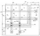
- FIG. 6is a schematic plan view of a dual-panel type OELD device according to a third embodiment of the present invention.
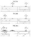
- FIGS. 7 and 8are cross-sectional views taken along the lines VII-VII and VIII-VIII of FIG. 6 ;
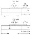
- FIGS. 9A to 9H and 10 A to 10 Hare cross-sectional views, which are taken along the lines VII-VII and VIII-VIII of FIG. 6 , illustrating a method of fabricating a first substrate for a dual-panel type OELD device according to the third embodiment of the present invention.
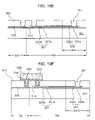
- FIG. 4Ais a cross-sectional view of a dual-panel type organic electroluminescent display (OELD) device according to a first embodiment of the present invention
- FIG. 4Bis a cross-sectional view of a data pad area of the OELD device of the FIG. 4A .
- OELDorganic electroluminescent display
- a dual-panel type OELD deviceincludes first and second substrates 101 and 171 facing and spaced apart from each other.
- a display area “DA” and a non-display area “NA” surrounding the display area “DA”are defined.
- a seal pattern 193is disposed in the non-display area “NA” and surrounds the display area “DA”.
- An organic electroluminescent (EL) diode “E”is disposed on an inner surface of the second substrate 171 .
- the organic EL diode “E”includes a first electrode 175 , an organic emitting layer 187 and a second electrode 190 that are sequentially disposed on the inner surface of the second substrate 171 .
- the first electrode 175is disposed on the entire inner surface of the second substrate 171 .
- First and second insulating patterns 177 and 178are formed on the first electrode 175 .
- a separator 181is formed on the first insulating pattern 177 and disposed between adjacent sub-pixel regions “SP”, and a spacer 184 is formed on the second insulating pattern 178 .
- the spacer 184has a height higher than the separator 181 such that the second electrode 190 contacts the connection electrode 155 .
- the organic emitting layer 187includes red (R), green (G) and blue (B) emitting layers 187 a , 187 b and 187 c .
- the organic emitting layer 187is disposed in each sub-pixel region “SP” and surrounded by the separator 181 . Also, the second electrode 190 on the organic emitting layer 187 is disposed in each sub-pixel region “SP” and surrounded by the separator 181 .
- the terms of anode and cathodeare used interchangeably and anode is generally made of a material having a work function higher than that of cathode.
- the first electrode 175can serve as either a cathode or anode in the OELD device, and when the first electrode 175 functions as a cathode, the second electrode 190 functions as an anode.
- the first and second electrodes 175 and 190function as an anode and a cathode, respectively, the first electrode 175 may have a work function higher than the second electrode 190 .
- the first electrode 175may be made of a transparent conductive material such as indium-tin-oxide (ITO) and indium-zinc-oxide (IZO) and the second electrode 190 may be made of an opaque conductive material such as alkaline metal, alkaline-earth metal, aluminum (Al), aluminum alloy (AlNd), copper (Cu), molybdenum (Mo), titanium (Ti) and an alloy thereof.
- the first and second electrodes 175 and 190may be made of an opaque conductive material and a transparent conductive material, respectively.
- a spacer 184is disposed on the inner surface of the second substrate 171 in each sub-pixel region “SP”.
- the spacer 184has a height higher than the separator 181 such that the second electrode 190 contacts a connection electrode 155 on the first substrate 101 .
- the organic emitting layer 187 in each sub-pixel region “SP”is separated by the spacer 184 .
- the second electrode 190is continuous in the sub-pixel region “SP” and includes a first portion on the organic emitting layer 187 and a second portion covering the spacer 184 . The second portion protruded by the spacer 184 contacts the connection electrode 155 .
- a gate line, and a data line and a power supply line crossing the gate linedefine the sub-pixel region “SP” on an inner surface of the first substrate 101 .
- an array element including a driving thin film transistor “Tr” and a switching thin film transistor (not shown)is disposed on the inner surface of the first substrate 101 .
- the driving thin film transistor “Tr”includes a gate electrode 109 on the first substrate 101 , an gate insulator 114 covering the gate electrode 109 , a semiconductor layer 120 on the gate insulator 114 , and source and drain electrodes 133 and 135 on the semiconductor layer 120 .
- the semiconductor layer 120includes an active layer 120 a and an ohmic contact layer 120 b .
- a passivation layer 145is disposed to cover the array element and the data line.
- the connection electrode 155is disposed on the passivation layer 145 in the sub-pixel region “SP” and contacts the drain electrode 135 through a drain contact hole 147 .
- gate and data pad electrodes 111 and 138are disposed at ends of the gate and data lines, respectively.
- the gate insulator 114 and the passivation layer 145 having a gate pad contact hole 149are disposed on the gate pad electrode 111 .
- the passivation layer 145 having a data pad contact hole 151is disposed on the data pad electrode 138 .
- Gate and data pad electrode terminals 157 and 160are disposed on the passivation layer 145 and contact the gate and data pad electrodes 111 and 138 through the gate and data pad contact holes 149 and 151 , respectively.
- connection electrode 155 contacting the second electrode 190may be made of the same material as the second electrode 190 for interface properties and contact resistivities between the connection electrode 155 and the second electrode 190 .
- the connection electrode 155 and the second electrode 190may be made of a conductive material such as aluminum (Al), aluminum alloy (AlNd), copper (Cu), molybdenum (Mo), titanium (Ti) and an alloy thereof.
- the gate and data pad electrode terminals 157 and 160which are exposed to air, may be made of a conductive material having a tolerance to corrosion, such as indium-tin-oxide (ITO) and indium-zinc-oxide (IZO).
- ITOindium-tin-oxide
- IZOindium-zinc-oxide
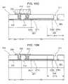
- FIG. 5Ais a cross-sectional view of a dual-panel type OELD device according to a second embodiment of the present invention
- FIG. 5Bis a cross-sectional view of a data pad area of the OELD device of the FIG. 5A
- the OELD device of the second embodimentis similar to the OELD device of the first embodiment, except for structures of gate and data pads. Accordingly, detailed explanation of the similar parts to the first embodiment will be omitted.
- gate and data pad electrode terminals 257 and 260have a double-layered structure.
- Lower layers 257 a and 260 a of the gate and data pad electrode terminals 257 and 260may be made of the same material as the connection electrode 255 and the second electrode 290 .
- the lower layers 257 a and 260 amay be made of a conductive material having a low work function, such as aluminum (Al) and aluminum alloy (AlNd).
- Upper layers 257 b and 260 b of the gate and data pad electrode terminals 257 and 260may be made of a conductive material having a tolerance to corrosion, such as indium-tin-oxide (ITO) and indium-zinc-oxide (IZO).
- ITOindium-tin-oxide
- IZOindium-zinc-oxide
- a corrosion of the gate and data pad electrode terminals 257 and 260can be minimized or prevented by forming the corrosion-proof upper layers 257 b and 260 b on the lower layers 257 a and 260 a that are susceptible to corrosion.
- the transparent conductive material having a tolerance to corrosionsuch as indium-tin-oxide (ITO) and indium-zinc-oxide (IZO) is used to prevent the gate and data pad electrode terminals from being corroded under an air condition.
- ITOindium-tin-oxide
- IZOindium-zinc-oxide
- FIG. 6is a schematic plan view of a dual-panel type OELD device according to a third embodiment of the present invention.
- the OELD devicehas a display area “DA” where a plurality of sub-pixel regions “SP” are arranged, and a non-display area “NA” where gate and data pads supplied with driving signals are arranged.
- the sub-pixel regions “SP”are defined by gate and data lines 305 and 330 crossing each other.
- an array element including a switching thin film transistor and a driving thin film transistoris disposed on a first substrate, and an organic EL diode including a first electrode, an organic emitting layer and a second electrode is disposed on a second substrate facing the first substrate.
- the gate line 305is extended along a first direction into a gate pad area “GPA” of the non-display area “NA”, and a gate pad electrode 309 is disposed at one end of the gate line 305 in the gate pad area “GPA”.
- the data line 330is extended along a second direction crossing the first direction into a boundary area between the display area “DA” and the non-display area “NA”.
- a data link line 307is spaced apart from the data line 330 and extended along the second direction in the non-display area “NA”, and a data pad electrode 338 is disposed at one end of the data link line 307 in a data pad area “DPA”.
- the data link line 307 and the data pad electrode 338are made of the same material as the gate line 305 .
- the data link line 307is connected to the data line 330 through a link pattern 356 , which extends across the boundary area between the display area “DA” and the non-display area “NA”.
- the link pattern 356contacts one end of the data line 330 through a first link contact hole 352 and contacts the other end of the data link line 307 through a second link contact hole 353 .
- a portion of the link pattern 356underlies a seal pattern 393 and the other portion of the link pattern 356 is surrounded by the seal pattern 393 , and thus the link pattern 356 is not exposed to air.
- the link pattern 356is surrounded by an outline of the seal pattern 393 . Accordingly, the link pattern 356 is not corroded because a space between the first and second substrates surrounded by the seal pattern 393 is under a vacuum condition or filled with an inert gas.
- FIGS. 7 and 8are cross-sectional views taken along lines the VII-VII and VIII-VIII of FIG. 6 .
- the OELD device of the third embodimentis similar to the OELD devices of the first and second embodiments, except for stacking structures of gate and data pads and connection structures of a data line and a data link line. Accordingly, detailed explanation of the similar parts to the first and second embodiments will be omitted.
- an array element including a driving thin film transistor “Tr” and a switching thin film transistor (not shown)is disposed in each sub-pixel “SP”.
- the driving thin film transistor “Tr”includes a gate electrode 309 on an inner surface of the first substrate 301 , an gate insulator 314 on the gate electrode 309 , a semiconductor layer 320 on the gate insulator 314 , and source and drain electrodes 333 and 335 on the semiconductor layer 320 .
- a passivation layer 345is disposed on the entire first substrate 301 having the driving thin film transistor “Tr”.
- a gate pad electrode 311is extended from a gate line ( 305 of FIG. 6 ) and is disposed at one end of the gate line. Also, a data link line 307 connected to the data line 330 is disposed in the non-display area “NA”, and a data pad electrode 338 is extended from the data link line 307 and disposed at one end of the data link line 307 in a data pad area “DPA”.
- the data link line 307 and the data pad electrode 338are made of the same material as the gate line and the gate pad electrode 311 and disposed at the same layer as the gate line and the gate pad electrode 311 .
- the gate line, gate pad electrode 311 , the data link line 307 and the data pad electrode 338have at least two layers.
- Lower layers 307 a , 311 a and 338 a of the gate line, the data link line 307 , the gate pad electrode 311 and the data pad electrode 338may be made of a transparent conductive material having a tolerance to corrosion, such as indium-tin-oxide (ITO) and indium-zinc-oxide (IZO).
- Upper layers 307 b , 311 b and 338 bmay be made of a conductive material having a low resistivity, such as aluminum (Al) or aluminum alloy (AlNd).
- the upper layer 307 b , 311 b or 338 b having a single-layered structureis illustrated in FIGS. 7 and 8
- the upper layermay have a double-layered structure, such as aluminum (Al)/molybdenum (Mo) or aluminum alloy (AlNd)/molybdenum (Mo).
- the gate insulator 314 and the passivation layer 345are sequentially disposed on the gate line, the data link line 307 , the gate pad electrode 311 and the data pad electrode 338 .
- the gate insulator 314 and the passivation layer 345have gate and data pad contact holes 349 and 351 exposing the gate and data pad electrodes 311 and 338 , respectively.
- the upper layers 311 b and 338 b of the gate and data pad electrodes 311 and 338are removed to have the gate and data pad contact holes 349 and 351 such that the lower layers 311 a and 338 a are exposed through the gate and data pad contact holes 349 and 351 .
- the upper layers 311 b and 338 bare susceptible to corrosion and the lower layers 311 a and 338 a have a tolerance to corrosion, the upper layers 311 b and 338 b are etched to expose the lower layers 331 a and 338 a . Accordingly, a corrosion of the gate and data pad electrodes 311 and 338 can be minimized or prevented.
- the passivation layer 345has a first link contact hole 352 exposing one end of the data line 330
- the passivation layer 345 and the gate insulator 314has a second link contact hole 353 exposing the other end of the data link line 307
- a link pattern 356connects the data line 330 and the data link line 307 through the first and second link contact holes 352 and 353 , respectively.
- the data line 330is connected to the data link line 307 through the link pattern 356 .
- a portion of the link pattern 356underlies a seal pattern 393 and the other portion of the link pattern 356 is surrounded by the seal pattern 393 .
- the other portion of the link pattern 356which is exposed on a space between the first and second substrates surrounded by the seal pattern 393 , is not corroded because the space is under a vacuum condition or filled with an inert gas.
- the portion of the link pattern 356 below the seal pattern 393is not corroded because the portion of the link pattern 356 does not contact exterior air due to the seal pattern 393 .
- the link pattern 356 that is not exposed to an air conditionmay be made of a conductive material having a low resistivity, although the material is susceptible to corrosion.
- the gate and data pad electrodeshas the lower layers having a tolerance to corrosion, and the lower layers are exposed to an air condition. Further, the link pattern is shielded from an air condition due to the seal pattern. Accordingly, a corrosion of the gate and data pad electrodes and the link pattern can be minimized or prevented.
- FIGS. 9A to 9H and 10 A to 10 Hare cross-sectional views, which are taken along the lines VII-VII and VIII-VIII of FIG. 6 , illustrating a method of fabricating a first substrate for a dual-panel type OELD device according to the third embodiment of the present invention.
- a first conductive material having a tolerance to corrosionsuch as indium-tin-oxide (ITO) and indium-zinc-oxide (IZO) is deposited on a first substrate 301 to form a first layer (a lower layer).
- a second conductive material having a low resistivityis deposited on the first layer to form a second layer (a upper layer).
- the second layermay have a single-layered structure made of one of aluminum (Al), aluminum alloy (AlNd), copper (Cu), molybdenum (Mo) and titanium (Ti), or a multi-layered structure made of at least two of the above materials.
- a mask processi.e., a photolithograph process is conducted to pattern the first and second layers, which includes depositing a photoresist on the first and second layers, exposing light with a mask, developing the photoresist, etching the first and second layers, and stripping or ashing the residual photoresist.
- a gate line305 of FIG. 6
- a gate electrode 309extended from the gate line
- GPAgate pad electrode 311 in a gate pad area
- NAnon-display area
- DPAdata pad electrode 338 in a data pad area
- Each of the gate line, the data link line 307 , the gate electrode 309 , the gate pad electrode 311 , and the data pad electrode 338has the patterned first layer (the lower layer) 307 a , 309 a , 311 a or 338 a , and the patterned second layer (the upper layer) 307 b , 309 b , 311 b or 338 b.
- an inorganic insulating materialis deposited on the entire substrate 101 having the gate electrode 309 to form a gate insulator 314 .
- the organic insulating materialmay be one of silicon oxide (SiO 2 ) and silicon nitride (SiNx).
- amorphous silicon (a-Si) and impurity-doped amorphous silicon (n+ a-Si)are sequentially deposited on the gate insulator 314 and patterned with a mask process to form a semiconductor layer 320 .
- the semiconductor layer 320includes an active layer 320 a of amorphous silicon and an ohmic contact layer 320 b of impurity-doped amorphous silicon.
- a third conductive materialis deposited on the substrate 301 having the semiconductor layer 320 and patterned with a mask process to form a data line 330 , and source and drain electrodes 333 and 335 .
- the third conductive materialmay be one of aluminum (Al), aluminum alloy (AlNd), chromium (Cr), molybdenum (Mo), titanium (Ti), copper (Cu) and copper alloy.
- the data line 330 , and the source and drain electrodes 333 and 335may have a multi-layered structure made of at least two of the above materials.
- the data line 330crosses the gate line to define a sub-pixel region “SP” in a display area “DA”.
- the gate electrode 309 , the gate insulator 314 , the semiconductor layer 320 and the source and drain electrodes 333 and 335form a driving thin film transistor “Tr”.
- a switching thin film transistoris formed simultaneously with the driving thin film transistor “Tr” and has a similar structure to the driving thin film transistor “Tr”.
- an organic insulating material or an inorganic insulating materialis deposited on the entire substrate 301 having the data line 330 to form a passivation layer 345 .
- the organic insulating materialmay be one of benzocyclobutene (BCB) and photo acrylic, and the inorganic insulating material may be one of silicon oxide (SiO 2 ) and silicon nitride (SiNx).
- the passivation layer 345is patterned with a mask process to form a drain contact hole 347 exposing the drain electrode 335 and a first link contact hole 352 exposing one end of the data line 330 .
- the gate insulator 314is patterned along with the passivation layer 345 to form a gate pad contact hole 349 exposing the gate pad electrode 311 , a data pad contact hole 351 exposing the data pad electrode 338 and a second link contact hole 353 exposing the other end of the data link line 307 .
- a fourth conductive materialis deposited on the passivation layer 345 , and a photoresist is deposited on the fourth conductive material.
- the fourth conductive materialmay include a material used for the second electrode ( 390 of FIG. 7 ), such as aluminum (Al) and aluminum alloy (AlNd) having a low work function. Exposing and developing processes for the photoresist are conducted to form a photoresist pattern 359 .
- the fourth conductive material layeris patterned with the photoresist pattern 359 to form a connection electrode 355 contacting the drain electrode 335 through the drain contact hole 347 , and a link pattern 356 contacting the data line 330 and the data link line 307 through the first and second link contact holes 352 and 353 , respectively.
- the photoresist pattern 359still remains on the connection electrode 355 and the link pattern 356 .
- a dry etching or wet etchingis conducted.
- the second layers (the upper layers) 311 b and 338 b of the gate and data pad electrodes 311 and 338 exposed through the gate and data pad contact holes 349 and 351are removed, and thus the first layers (the lower layers) 311 a and 338 a of the gate and data pad electrodes 311 and 338 are exposed.
- the second layers 311 b and 338 b that have a low resistivity and are susceptible to corrosionare removed by the etching process, and the first layers 311 a and 338 b having a tolerance to corrosion are exposed.
- the photoresist pattern( 359 of FIGS. 9G and 10G ) is removed by a stripping or ashing process.
- the first substrate for the dual-panel type OELD device according to the third embodimentis fabricated.
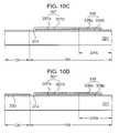
- a fabrication method of the second substrate for the dual-panel type OELD deviceis described with reference to FIGS. 7 and 8 .
- the first electrode 375is formed on the entire second substrate 371 .
- the first electrode 375may be made of a transparent conductive material such as indium-tin-oxide (ITO) and indium-zinc-oxide (IZO) having a high work function.
- ITOindium-tin-oxide
- IZOindium-zinc-oxide
- the first and second electrodes 375 and 390act as an anode and a cathode, respectively.
- first and second insulating patterns 377 and 378An inorganic insulating material is deposited on the first electrode 375 and patterned to form first and second insulating patterns 377 and 378 .
- the first insulating pattern 377is formed between adjacent sub-pixel regions “SP”, and the second insulating pattern 378 is formed in the sub-pixel region “SP”.
- An organic insulating materialis deposited on the substrate 371 having the insulating patterns 377 and 378 and patterned to form a separator 381 and a spacer 384 .
- the separator 381is formed on the first insulating pattern 377
- the spacer 384is formed on the second insulating pattern 378 .
- the spacer 384has a height higher than the separator 381 such that the second electrode 390 contacts the connection electrode 355 .
- a diffraction exposure method or a halftone exposure methodmay be used.
- a photoresistis deposited on the organic insulating material used for the separator 381 and the spacer 384 .
- a diffraction exposure or a halftone exposure to the photoresistis conducted to form first and second photoresist patterns corresponding to the first and second insulating patterns 377 and 378 , respectively, and portions of the photoresist except for the first and second photoresist patterns are removed.
- the second photoresist patternhas a height higher than the first photoresist pattern.
- the organic insulating material exposed through the first and second photoresist patternsis removed to form first and second organic insulating patterns below the first and second photoresist patterns, respectively.
- the first photoresist patternis removed by a stripping or ashing process.
- the second photoresist patternis partially removed and remains on the second organic insulating pattern.
- the first organic insulating patternis partially removed by a predetermined thickness.
- the second organic insulating patternis not removed due to the second photoresist pattern. Accordingly, the second organic insulating pattern has a height higher than the first insulating pattern.
- the second photoresist patternis removed.
- red (R), green (G) and blue (B) organic emitting materialsare sequentially coated to form red (R), green (G) and blue (B) organic emitting layers 387 a , 387 b and 387 c in respective sub-pixel regions “SP”. If the organic emitting layer 387 is formed by an evaporation method using a shadow mask, not by a coating method, the separator 381 and the first insulating pattern 377 may not be formed.
- the second electrode 390is formed on the organic emitting layer 387 in each sub-pixel region “SP”.
- the second electrode 390is separated by the separator 371 .
- the second electrode 390is continuous in the sub-pixel region “SP” and includes a first portion on the organic emitting layer 387 and a second portion covering the spacer 384 .
- the second portion protruded by the spacer 384contacts the connection electrode 355 .
- the second electrode 390When the second electrode 390 functions as a cathode, it may be made of aluminum (Al) and aluminum alloy (AlNd) having a lower work function than the first electrode 375 .
- first and second electrodes 375 and 390act as an anode and a cathode, respectively, a hole injection layer and a hole transmitting layer are sequentially formed between the first electrode 375 and the organic emitting layer 387 , and an electron injection layer and an electron transmitting layer may be formed between the second electrode 390 and the organic emitting layer 387 .
- a seal pattern 393is formed along a peripheral portion of one of the first and second substrates 301 and 371 . Under a vacuum condition or an inert gas condition, the first and second substrates 301 and 371 are attached with the seal pattern 393 such that the protruded portion of the second electrode 390 on the spacer 384 contacts the connection pattern 355 . Therefore, the dual-panel type OELD device is fabricated.
- a conductive material having a tolerance to corrosionis used for the layers of the gate and data pads exposed to an air condition. Accordingly, a corrosion of the gate and data pads can be minimized or prevented.
Landscapes
- Engineering & Computer Science (AREA)
- Microelectronics & Electronic Packaging (AREA)
- Physics & Mathematics (AREA)
- Computer Hardware Design (AREA)
- General Physics & Mathematics (AREA)
- Theoretical Computer Science (AREA)
- Manufacturing & Machinery (AREA)
- Electroluminescent Light Sources (AREA)
- Devices For Indicating Variable Information By Combining Individual Elements (AREA)
Abstract
Description
Claims (44)
Applications Claiming Priority (2)
| Application Number | Priority Date | Filing Date | Title |
|---|---|---|---|
| KR1020040099089AKR100603836B1 (en) | 2004-11-30 | 2004-11-30 | Organic electroluminescent device and manufacturing method thereof |
| KR2004-0099089 | 2004-11-30 |
Publications (2)
| Publication Number | Publication Date |
|---|---|
| US20060113903A1 US20060113903A1 (en) | 2006-06-01 |
| US7309955B2true US7309955B2 (en) | 2007-12-18 |
Family
ID=36371629
Family Applications (1)
| Application Number | Title | Priority Date | Filing Date |
|---|---|---|---|
| US11/267,284ActiveUS7309955B2 (en) | 2004-11-30 | 2005-11-07 | Organic electroluminescent display device and fabricating method thereof |
Country Status (8)
| Country | Link |
|---|---|
| US (1) | US7309955B2 (en) |
| JP (1) | JP4333922B2 (en) |
| KR (1) | KR100603836B1 (en) |
| CN (1) | CN100395894C (en) |
| DE (1) | DE102005056911B4 (en) |
| FR (1) | FR2878650B1 (en) |
| GB (1) | GB2420651B (en) |
| TW (1) | TWI315589B (en) |
Cited By (9)
| Publication number | Priority date | Publication date | Assignee | Title |
|---|---|---|---|---|
| US20070152222A1 (en)* | 2005-12-29 | 2007-07-05 | In Su Joo | Organic electro-luminescence display device and method of manfacturing the same |
| DE102008026216A1 (en)* | 2008-05-30 | 2009-12-03 | Polyic Gmbh & Co. Kg | Electronic switch |
| CN101604703A (en)* | 2008-06-11 | 2009-12-16 | 三星移动显示器株式会社 | Organic light-emitting diode (OLED) display apparatus and forming method thereof |
| US20090309109A1 (en)* | 2008-06-11 | 2009-12-17 | Seung Wook Chang | Organic light emitting diode display device and method of manufacturing the same |
| US20140176399A1 (en)* | 2012-12-21 | 2014-06-26 | Lg Display Co., Ltd. | Device display |
| US9142795B2 (en) | 2013-05-29 | 2015-09-22 | Samsung Display Co., Ltd. | Organic light-emitting diode |
| US10923539B2 (en)* | 2018-09-07 | 2021-02-16 | Samsung Display Co., Ltd. | Electronic display apparatus including a solar cell unit |
| US20220139970A1 (en)* | 2020-11-02 | 2022-05-05 | Samsung Display Co., Ltd. | Display apparatus and method of manufacturing the same |
| US12262606B2 (en) | 2019-08-06 | 2025-03-25 | Samsung Display Co., Ltd. | Display device including conductive member electrically connected to power line |
Families Citing this family (52)
| Publication number | Priority date | Publication date | Assignee | Title |
|---|---|---|---|---|
| US7485893B2 (en)* | 2005-07-08 | 2009-02-03 | Lg Display Co., Ltd. | Display device |
| KR100742642B1 (en)* | 2005-07-11 | 2007-07-25 | 네오뷰코오롱 주식회사 | Organic electroluminescent display panels, panel arrays and methods of manufacturing the same |
| KR100638143B1 (en) | 2005-10-12 | 2006-10-25 | 엘지전자 주식회사 | Organic electroluminescent display device and manufacturing method thereof |
| KR100713227B1 (en)* | 2006-06-30 | 2007-05-02 | 삼성전자주식회사 | Display device and manufacturing method thereof |
| KR101254644B1 (en)* | 2006-06-30 | 2013-04-15 | 엘지디스플레이 주식회사 | Organic electro-luminescence dispaly and fabricating method tererof |
| KR20080006316A (en)* | 2006-07-12 | 2008-01-16 | 삼성전자주식회사 | Organic thin film transistor and its manufacturing method |
| KR101318242B1 (en)* | 2007-01-26 | 2013-10-16 | 엘지디스플레이 주식회사 | Method of manufacturing flexible display device |
| JP5151172B2 (en)* | 2007-02-14 | 2013-02-27 | ソニー株式会社 | Pixel circuit and display device |
| KR100872709B1 (en)* | 2007-02-26 | 2008-12-05 | 엘지디스플레이 주식회사 | Organic light emitting display device and manufacturing method |
| KR100805124B1 (en)* | 2007-03-05 | 2008-02-21 | 삼성에스디아이 주식회사 | Manufacturing Method of Display Device and Display Device |
| KR100836472B1 (en) | 2007-03-22 | 2008-06-09 | 삼성에스디아이 주식회사 | Semiconductor device and manufacturing method |
| JP4993292B2 (en)* | 2007-07-18 | 2012-08-08 | カシオ計算機株式会社 | Display panel and manufacturing method thereof |
| JP4506810B2 (en) | 2007-10-19 | 2010-07-21 | ソニー株式会社 | Display device |
| KR101496215B1 (en)* | 2008-03-17 | 2015-02-27 | 삼성디스플레이 주식회사 | Thin film transistor substrate and method for manufacturing the same |
| JP5541872B2 (en) | 2009-02-26 | 2014-07-09 | パナソニック株式会社 | Planar light emitting device and lighting apparatus |
| KR101287478B1 (en)* | 2009-06-02 | 2013-07-19 | 엘지디스플레이 주식회사 | Display device having oxide thin film transistor and method of fabricating thereof |
| KR101073552B1 (en) | 2009-10-09 | 2011-10-17 | 삼성모바일디스플레이주식회사 | Organic light emitting diode display and method of manufacturing the same |
| JP2011100011A (en)* | 2009-11-06 | 2011-05-19 | Mitsubishi Electric Corp | Display device |
| KR101641363B1 (en)* | 2010-02-22 | 2016-08-01 | 엘지디스플레이 주식회사 | Organic light emitting display device |
| JP2011233512A (en)* | 2010-04-07 | 2011-11-17 | Sumitomo Chemical Co Ltd | Light emitting device |
| KR101664182B1 (en)* | 2010-04-27 | 2016-10-10 | 엘지디스플레이 주식회사 | Organic electro-luminescent device |
| KR20120032904A (en)* | 2010-09-29 | 2012-04-06 | 삼성모바일디스플레이주식회사 | Organic light emitting display apparatus and method of manufacturing thereof |
| KR101811702B1 (en)* | 2010-10-27 | 2017-12-26 | 삼성디스플레이 주식회사 | Organinc light emitting display device and manufacturing method for the same |
| KR101815255B1 (en)* | 2010-12-16 | 2018-01-08 | 삼성디스플레이 주식회사 | Organic light emitting display device and input pad thereof |
| WO2013011602A1 (en)* | 2011-07-19 | 2013-01-24 | パナソニック株式会社 | Display device and method for manufacturing display device |
| KR101860036B1 (en)* | 2011-11-15 | 2018-06-28 | 엘지디스플레이 주식회사 | Chip on glass type flexible organic light emitting diodes |
| KR101871773B1 (en) | 2012-07-25 | 2018-06-27 | 엘지디스플레이 주식회사 | Plastic panel and flat panel display device using the same |
| KR101968929B1 (en)* | 2012-09-11 | 2019-04-16 | 삼성디스플레이 주식회사 | Sensor substrate, method of manufacturing the same and sensing display panel having the same |
| KR102025835B1 (en)* | 2012-11-26 | 2019-11-27 | 삼성디스플레이 주식회사 | Display apparatus and organic luminescense display apparatus |
| KR102020353B1 (en) | 2013-03-20 | 2019-11-05 | 삼성디스플레이 주식회사 | Display apparatus and method of manufacturing the same |
| KR102223676B1 (en) | 2014-06-24 | 2021-03-08 | 삼성디스플레이 주식회사 | Display device |
| KR102320186B1 (en)* | 2014-07-18 | 2021-10-29 | 엘지디스플레이 주식회사 | Organic light emitting display device and method of fabricating the same |
| KR102204785B1 (en)* | 2014-07-25 | 2021-01-19 | 엘지디스플레이 주식회사 | Organic light emitting diode display device and fabricating method of the same |
| KR102192227B1 (en)* | 2014-10-02 | 2020-12-17 | 엘지디스플레이 주식회사 | Pad structure and display device having the same |
| KR102317553B1 (en)* | 2015-08-28 | 2021-10-25 | 엘지디스플레이 주식회사 | Organic light emitting display device |
| CN105789115A (en) | 2016-04-26 | 2016-07-20 | 京东方科技集团股份有限公司 | Via hole manufacturing method, array substrate and manufacturing method thereof and display device |
| KR102404573B1 (en)* | 2016-05-27 | 2022-06-03 | 삼성디스플레이 주식회사 | Display device |
| KR102777195B1 (en)* | 2016-10-13 | 2025-03-06 | 삼성디스플레이 주식회사 | Organic light emitting display device |
| KR20180061866A (en)* | 2016-11-30 | 2018-06-08 | 엘지디스플레이 주식회사 | Encapsulation unit and organic light emitting display including the same |
| CN107170773B (en)* | 2017-05-23 | 2019-09-17 | 深圳市华星光电技术有限公司 | Micro- LED display panel and preparation method thereof |
| CN107966841B (en)* | 2017-12-28 | 2020-06-02 | 友达光电(昆山)有限公司 | Display device |
| CN110459505B (en)* | 2018-05-07 | 2022-01-11 | 京东方科技集团股份有限公司 | Via hole connection structure, array substrate manufacturing method and array substrate |
| KR102528500B1 (en)* | 2018-07-19 | 2023-05-04 | 삼성디스플레이 주식회사 | Display apparatus |
| CN112823568B (en)* | 2018-09-25 | 2024-06-14 | 夏普株式会社 | Display device |
| KR102796783B1 (en)* | 2019-03-07 | 2025-04-16 | 삼성디스플레이 주식회사 | Organic light emitting display device |
| KR102806404B1 (en)* | 2019-06-13 | 2025-05-13 | 삼성디스플레이 주식회사 | Display Apparatus |
| KR102657663B1 (en) | 2019-07-31 | 2024-04-16 | 삼성디스플레이 주식회사 | Backiight unit and display device including the same |
| KR102182538B1 (en)* | 2019-09-20 | 2020-11-25 | 삼성디스플레이 주식회사 | Display apparatus and organic luminescense display apparatus |
| KR20210054636A (en)* | 2019-11-05 | 2021-05-14 | 삼성디스플레이 주식회사 | Display device |
| KR20210100795A (en)* | 2020-02-06 | 2021-08-18 | 삼성디스플레이 주식회사 | Display device |
| CN114188379A (en)* | 2021-12-02 | 2022-03-15 | 深圳市华星光电半导体显示技术有限公司 | Display panel and display device |
| KR20230092217A (en)* | 2021-12-17 | 2023-06-26 | 엘지디스플레이 주식회사 | Organic light emitting diode and method for manufacturing thereof |
Citations (25)
| Publication number | Priority date | Publication date | Assignee | Title |
|---|---|---|---|---|
| US20020110941A1 (en)* | 2000-01-26 | 2002-08-15 | Shunpei Yamazaki | Semiconductor device and manufacturing method thereof |
| US6498428B1 (en)* | 1996-02-26 | 2002-12-24 | Idemitsu Kosan Co., Ltd. | Organic electroluminescent element and method for manufacturing same |
| US20030146696A1 (en)* | 2001-12-29 | 2003-08-07 | Lg.Philips Lcd Co., Ltd. | Active matrix organic electroluminescent display and fabricating method thereof |
| US20030201445A1 (en)* | 2002-04-25 | 2003-10-30 | Lg.Philips Lcd Co., Ltd. | Organic electroluminescent display device |
| US20040017151A1 (en)* | 2002-07-25 | 2004-01-29 | Lg.Philips Lcd Co. | Organic electroluminescent display device and method of fabricating the same |
| US20040036410A1 (en)* | 2002-08-20 | 2004-02-26 | Lg. Philips Lcd Co., Ltd. | Organic electroluminescent display device and method of fabricating the same |
| US20040080266A1 (en)* | 2002-07-08 | 2004-04-29 | Lg.Philips Lcd Co., Ltd. | Active matrix organic electroluminescent display device and method of fabricating the same |
| US6744197B2 (en)* | 2002-05-03 | 2004-06-01 | Lg.Philips Lcd Co., Ltd. | Organic electroluminescent display device and method of fabricating the same |
| US20040135520A1 (en)* | 2002-12-26 | 2004-07-15 | Lg.Philips Lcd Co., Ltd. | Organic electroluminescent device and manufacturing method for the same |
| US20040145306A1 (en)* | 2002-12-26 | 2004-07-29 | Lg.Philips Lcd Co., Ltd. | Dual panel type organic electroluminescent display device and manufacturing method for the same |
| US20040195959A1 (en)* | 2002-12-28 | 2004-10-07 | Lg.Philips Lcd Co., Ltd. | Dual panel-type organic electroluminescent device and method for fabricating the same |
| US6828587B2 (en)* | 2000-06-19 | 2004-12-07 | Semiconductor Energy Laboratory Co., Ltd. | Semiconductor device |
| US20050028860A1 (en)* | 1998-02-26 | 2005-02-10 | Canon Kabushiki Kaisha | Stacked photovoltaic device |
| US20050127828A1 (en)* | 2003-11-28 | 2005-06-16 | Jin-Koo Chung | Organic light emitting display and manufacturing method thereof |
| US20050140285A1 (en)* | 2003-12-30 | 2005-06-30 | Lg.Philips Lcd Co., Ltd. | Dual panel type organic electroluminescent display device and method of fabricating the same |
| US20050140282A1 (en)* | 2003-12-30 | 2005-06-30 | Lg.Philips Lcd Co., Ltd. | Organic electroluminescent display device and method of fabricating the same |
| US20050140281A1 (en)* | 2003-12-29 | 2005-06-30 | Lg.Philips Lcd Co., Ltd. | Organic electroluminescent display device and method of fabricating the same |
| US20050139839A1 (en)* | 2003-12-26 | 2005-06-30 | Lg.Philips Lcd Co., Ltd. | Dual panel-type organic electroluminescent display device and method of fabricating the same |
| US6922015B2 (en)* | 2002-04-25 | 2005-07-26 | Lg.Philips Lcd Co., Ltd. | Organic electroluminescent display device and method of fabricating the same |
| US20050179374A1 (en)* | 2004-02-14 | 2005-08-18 | Won-Kyu Kwak | Organic electro-luminescent display device and method of manufacturing the same |
| US20050236956A1 (en)* | 2004-04-19 | 2005-10-27 | L.G.Philips Lcd Co. Inc. | Organic electroluminescent display device and fabricating method thereof |
| US6982524B2 (en)* | 2002-11-13 | 2006-01-03 | Lg.Philips Lcd Co., Ltd. | Dual panel-type organic electroluminescent display device and method of fabricating the same |
| US7105999B2 (en)* | 2002-07-05 | 2006-09-12 | Lg.Philips Lcd Co., Ltd. | Organic electroluminescent display device and method of fabricating the same |
| US7116044B2 (en)* | 2000-05-08 | 2006-10-03 | Semiconductor Energy Laboratory Co., Ltd. | Luminescent apparatus and method of manufacturing the same |
| US7232702B2 (en)* | 2002-12-26 | 2007-06-19 | Lg.Philips Lcd Co., Ltd. | Dual panel type organic electroluminescent device and method of fabricating the same |
Family Cites Families (3)
| Publication number | Priority date | Publication date | Assignee | Title |
|---|---|---|---|---|
| US6699728B2 (en)* | 2000-09-06 | 2004-03-02 | Osram Opto Semiconductors Gmbh | Patterning of electrodes in oled devices |
| JP2003066859A (en) | 2001-08-28 | 2003-03-05 | Sharp Corp | Display device and method of manufacturing the same |
| TWI272872B (en) | 2002-12-13 | 2007-02-01 | Lg Philips Lcd Co Ltd | Dual panel-type organic electroluminescent display device and method of fabricating the same |
- 2004
- 2004-11-30KRKR1020040099089Apatent/KR100603836B1/ennot_activeExpired - Lifetime
- 2005
- 2005-11-07USUS11/267,284patent/US7309955B2/enactiveActive
- 2005-11-07GBGB0522687Apatent/GB2420651B/enactiveActive
- 2005-11-11TWTW094139616Apatent/TWI315589B/enactive
- 2005-11-16CNCNB2005101153857Apatent/CN100395894C/enactiveActive
- 2005-11-18FRFR0511700Apatent/FR2878650B1/enactiveActive
- 2005-11-29DEDE102005056911Apatent/DE102005056911B4/enactiveActive
- 2005-11-30JPJP2005345623Apatent/JP4333922B2/enactiveActive
Patent Citations (28)
| Publication number | Priority date | Publication date | Assignee | Title |
|---|---|---|---|---|
| US6498428B1 (en)* | 1996-02-26 | 2002-12-24 | Idemitsu Kosan Co., Ltd. | Organic electroluminescent element and method for manufacturing same |
| US20050028860A1 (en)* | 1998-02-26 | 2005-02-10 | Canon Kabushiki Kaisha | Stacked photovoltaic device |
| US20020110941A1 (en)* | 2000-01-26 | 2002-08-15 | Shunpei Yamazaki | Semiconductor device and manufacturing method thereof |
| US6825488B2 (en)* | 2000-01-26 | 2004-11-30 | Semiconductor Energy Laboratory Co., Ltd. | Semiconductor device and manufacturing method thereof |
| US7116044B2 (en)* | 2000-05-08 | 2006-10-03 | Semiconductor Energy Laboratory Co., Ltd. | Luminescent apparatus and method of manufacturing the same |
| US6828587B2 (en)* | 2000-06-19 | 2004-12-07 | Semiconductor Energy Laboratory Co., Ltd. | Semiconductor device |
| US20030146696A1 (en)* | 2001-12-29 | 2003-08-07 | Lg.Philips Lcd Co., Ltd. | Active matrix organic electroluminescent display and fabricating method thereof |
| US6922015B2 (en)* | 2002-04-25 | 2005-07-26 | Lg.Philips Lcd Co., Ltd. | Organic electroluminescent display device and method of fabricating the same |
| US20030201445A1 (en)* | 2002-04-25 | 2003-10-30 | Lg.Philips Lcd Co., Ltd. | Organic electroluminescent display device |
| US6744197B2 (en)* | 2002-05-03 | 2004-06-01 | Lg.Philips Lcd Co., Ltd. | Organic electroluminescent display device and method of fabricating the same |
| US7105999B2 (en)* | 2002-07-05 | 2006-09-12 | Lg.Philips Lcd Co., Ltd. | Organic electroluminescent display device and method of fabricating the same |
| US20040080266A1 (en)* | 2002-07-08 | 2004-04-29 | Lg.Philips Lcd Co., Ltd. | Active matrix organic electroluminescent display device and method of fabricating the same |
| US7109650B2 (en)* | 2002-07-08 | 2006-09-19 | Lg.Philips Lcd Co., Ltd. | Active matrix organic electroluminescent display device and method of fabricating the same |
| US20040017151A1 (en)* | 2002-07-25 | 2004-01-29 | Lg.Philips Lcd Co. | Organic electroluminescent display device and method of fabricating the same |
| US6927536B2 (en)* | 2002-07-25 | 2005-08-09 | Lg.Philips Lcd Co., Ltd. | Organic electroluminescent display device with insulating layer patterns and method of fabricating the same |
| US20040036410A1 (en)* | 2002-08-20 | 2004-02-26 | Lg. Philips Lcd Co., Ltd. | Organic electroluminescent display device and method of fabricating the same |
| US6982524B2 (en)* | 2002-11-13 | 2006-01-03 | Lg.Philips Lcd Co., Ltd. | Dual panel-type organic electroluminescent display device and method of fabricating the same |
| US7232702B2 (en)* | 2002-12-26 | 2007-06-19 | Lg.Philips Lcd Co., Ltd. | Dual panel type organic electroluminescent device and method of fabricating the same |
| US20040145306A1 (en)* | 2002-12-26 | 2004-07-29 | Lg.Philips Lcd Co., Ltd. | Dual panel type organic electroluminescent display device and manufacturing method for the same |
| US20040135520A1 (en)* | 2002-12-26 | 2004-07-15 | Lg.Philips Lcd Co., Ltd. | Organic electroluminescent device and manufacturing method for the same |
| US20040195959A1 (en)* | 2002-12-28 | 2004-10-07 | Lg.Philips Lcd Co., Ltd. | Dual panel-type organic electroluminescent device and method for fabricating the same |
| US20050127828A1 (en)* | 2003-11-28 | 2005-06-16 | Jin-Koo Chung | Organic light emitting display and manufacturing method thereof |
| US20050139839A1 (en)* | 2003-12-26 | 2005-06-30 | Lg.Philips Lcd Co., Ltd. | Dual panel-type organic electroluminescent display device and method of fabricating the same |
| US20050140281A1 (en)* | 2003-12-29 | 2005-06-30 | Lg.Philips Lcd Co., Ltd. | Organic electroluminescent display device and method of fabricating the same |
| US20050140282A1 (en)* | 2003-12-30 | 2005-06-30 | Lg.Philips Lcd Co., Ltd. | Organic electroluminescent display device and method of fabricating the same |
| US20050140285A1 (en)* | 2003-12-30 | 2005-06-30 | Lg.Philips Lcd Co., Ltd. | Dual panel type organic electroluminescent display device and method of fabricating the same |
| US20050179374A1 (en)* | 2004-02-14 | 2005-08-18 | Won-Kyu Kwak | Organic electro-luminescent display device and method of manufacturing the same |
| US20050236956A1 (en)* | 2004-04-19 | 2005-10-27 | L.G.Philips Lcd Co. Inc. | Organic electroluminescent display device and fabricating method thereof |
Cited By (20)
| Publication number | Priority date | Publication date | Assignee | Title |
|---|---|---|---|---|
| US8017950B2 (en)* | 2005-12-29 | 2011-09-13 | Lg Display Co., Ltd. | Organic electro-luminescence display device and method of manfacturing the same |
| US20070152222A1 (en)* | 2005-12-29 | 2007-07-05 | In Su Joo | Organic electro-luminescence display device and method of manfacturing the same |
| US8350259B2 (en) | 2008-05-30 | 2013-01-08 | Polyic Gmbh & Co. Kg | Electronic circuit |
| US20110115101A1 (en)* | 2008-05-30 | 2011-05-19 | Alexander Knobloch | Electronic circuit |
| DE102008026216A1 (en)* | 2008-05-30 | 2009-12-03 | Polyic Gmbh & Co. Kg | Electronic switch |
| DE102008026216B4 (en)* | 2008-05-30 | 2010-07-29 | Polyic Gmbh & Co. Kg | Electronic switch |
| CN101604703B (en)* | 2008-06-11 | 2013-05-08 | 三星显示有限公司 | Organic light emitting diode display device and method of manufacturing the same |
| US7829887B2 (en)* | 2008-06-11 | 2010-11-09 | Samsung Mobile Display Co., Ltd. | Organic light emitting diode display device and method of manufacturing the same |
| CN101604703A (en)* | 2008-06-11 | 2009-12-16 | 三星移动显示器株式会社 | Organic light-emitting diode (OLED) display apparatus and forming method thereof |
| US20090309109A1 (en)* | 2008-06-11 | 2009-12-17 | Seung Wook Chang | Organic light emitting diode display device and method of manufacturing the same |
| US20090309108A1 (en)* | 2008-06-11 | 2009-12-17 | Seung Wook Chang | Organic light emitting diode display device and method of manufacturing the same |
| US7829888B2 (en)* | 2008-06-11 | 2010-11-09 | Samsung Mobile Display Co., Ltd. | Organic light emitting diode display device and method of manufacturing the same |
| US9384687B2 (en)* | 2012-12-21 | 2016-07-05 | Lg Display Co., Ltd. | Device display |
| US20140176399A1 (en)* | 2012-12-21 | 2014-06-26 | Lg Display Co., Ltd. | Device display |
| US9142795B2 (en) | 2013-05-29 | 2015-09-22 | Samsung Display Co., Ltd. | Organic light-emitting diode |
| US10923539B2 (en)* | 2018-09-07 | 2021-02-16 | Samsung Display Co., Ltd. | Electronic display apparatus including a solar cell unit |
| US11222932B2 (en) | 2018-09-07 | 2022-01-11 | Samsung Display Co., Ltd. | Electronic display apparatus including a solar cell unit |
| US12262606B2 (en) | 2019-08-06 | 2025-03-25 | Samsung Display Co., Ltd. | Display device including conductive member electrically connected to power line |
| US20220139970A1 (en)* | 2020-11-02 | 2022-05-05 | Samsung Display Co., Ltd. | Display apparatus and method of manufacturing the same |
| US12002821B2 (en)* | 2020-11-02 | 2024-06-04 | Samsung Display Co., Ltd. | Display apparatus and method of manufacturing the same |
Also Published As
| Publication number | Publication date |
|---|---|
| CN100395894C (en) | 2008-06-18 |
| TWI315589B (en) | 2009-10-01 |
| TW200620733A (en) | 2006-06-16 |
| GB2420651B (en) | 2007-05-02 |
| DE102005056911B4 (en) | 2011-08-18 |
| GB2420651A (en) | 2006-05-31 |
| FR2878650B1 (en) | 2011-10-14 |
| FR2878650A1 (en) | 2006-06-02 |
| DE102005056911A1 (en) | 2006-06-01 |
| JP4333922B2 (en) | 2009-09-16 |
| KR100603836B1 (en) | 2006-07-24 |
| CN1783508A (en) | 2006-06-07 |
| US20060113903A1 (en) | 2006-06-01 |
| GB0522687D0 (en) | 2005-12-14 |
| JP2006156403A (en) | 2006-06-15 |
| KR20060060179A (en) | 2006-06-05 |
Similar Documents
| Publication | Publication Date | Title |
|---|---|---|
| US7309955B2 (en) | Organic electroluminescent display device and fabricating method thereof | |
| US11121198B2 (en) | Organic light emitting display device having auxiliary connection electrode and method of manufacturing the same | |
| US10672339B2 (en) | Organic light-emitting display device | |
| US8404509B2 (en) | Organic electroluminescent display device and method for fabricating the same | |
| US10403696B2 (en) | Organic light emitting display device and method of fabricating the same | |
| US7064350B2 (en) | Organic electroluminescent display device and method of fabricating the same | |
| US11839110B2 (en) | Organic light-emitting display device | |
| KR101352105B1 (en) | Organic light emitting display and method for fabricating the same | |
| US20240423052A1 (en) | Display panel and method for manufacturing same | |
| US7932671B2 (en) | Organic electroluminescent display device and method of fabricating the same | |
| KR101100891B1 (en) | Thin film transistor substrate and display device including same | |
| US7271017B2 (en) | Organic electroluminescent display device and fabricating method thereof | |
| KR102119572B1 (en) | Thin film transistor array substrate and method for fabricating the same | |
| KR20160060835A (en) | Organic Light Emitting Diode Display Device and Method of Fabricating the Same | |
| KR101469477B1 (en) | Organic light emitting display and manufacturing method thereof | |
| US8927970B2 (en) | Organic electroluminescence device and method for manufacturing the same | |
| KR101992914B1 (en) | Organic light emitting display and fabricating method thereof | |
| CN114975550A (en) | Display panel, manufacturing method and electronic equipment | |
| KR20070118795A (en) | Manufacturing method of dual panel type organic light emitting device | |
| KR20100020167A (en) | Organic light emitting display and method for fabricating the same | |
| KR20090131397A (en) | OLED display device and manufacturing method |
Legal Events
| Date | Code | Title | Description |
|---|---|---|---|
| AS | Assignment | Owner name:LG.PHILIPS LCD CO., LTD., KOREA, REPUBLIC OF Free format text:ASSIGNMENT OF ASSIGNORS INTEREST;ASSIGNOR:KIM, OCK-HEE;REEL/FRAME:017194/0719 Effective date:20051031 | |
| STCF | Information on status: patent grant | Free format text:PATENTED CASE | |
| FEPP | Fee payment procedure | Free format text:PAYOR NUMBER ASSIGNED (ORIGINAL EVENT CODE: ASPN); ENTITY STATUS OF PATENT OWNER: LARGE ENTITY | |
| AS | Assignment | Owner name:LG DISPLAY CO., LTD., KOREA, REPUBLIC OF Free format text:CHANGE OF NAME;ASSIGNOR:LG.PHILIPS LCD CO., LTD.;REEL/FRAME:021763/0177 Effective date:20080304 Owner name:LG DISPLAY CO., LTD.,KOREA, REPUBLIC OF Free format text:CHANGE OF NAME;ASSIGNOR:LG.PHILIPS LCD CO., LTD.;REEL/FRAME:021763/0177 Effective date:20080304 | |
| FEPP | Fee payment procedure | Free format text:PAYER NUMBER DE-ASSIGNED (ORIGINAL EVENT CODE: RMPN); ENTITY STATUS OF PATENT OWNER: LARGE ENTITY Free format text:PAYOR NUMBER ASSIGNED (ORIGINAL EVENT CODE: ASPN); ENTITY STATUS OF PATENT OWNER: LARGE ENTITY | |
| FPAY | Fee payment | Year of fee payment:4 | |
| FPAY | Fee payment | Year of fee payment:8 | |
| MAFP | Maintenance fee payment | Free format text:PAYMENT OF MAINTENANCE FEE, 12TH YEAR, LARGE ENTITY (ORIGINAL EVENT CODE: M1553); ENTITY STATUS OF PATENT OWNER: LARGE ENTITY Year of fee payment:12 |