US7309914B2 - Inverted CSP stacking system and method - Google Patents
Inverted CSP stacking system and methodDownload PDFInfo
- Publication number
- US7309914B2 US7309914B2US11/039,615US3961505AUS7309914B2US 7309914 B2US7309914 B2US 7309914B2US 3961505 AUS3961505 AUS 3961505AUS 7309914 B2US7309914 B2US 7309914B2
- Authority
- US
- United States
- Prior art keywords
- csp
- contacts
- module
- csps
- flex
- Prior art date
- Legal status (The legal status is an assumption and is not a legal conclusion. Google has not performed a legal analysis and makes no representation as to the accuracy of the status listed.)
- Expired - Lifetime, expires
Links
Images


Classifications
- H—ELECTRICITY
- H05—ELECTRIC TECHNIQUES NOT OTHERWISE PROVIDED FOR
- H05K—PRINTED CIRCUITS; CASINGS OR CONSTRUCTIONAL DETAILS OF ELECTRIC APPARATUS; MANUFACTURE OF ASSEMBLAGES OF ELECTRICAL COMPONENTS
- H05K1/00—Printed circuits
- H05K1/02—Details
- H05K1/14—Structural association of two or more printed circuits
- H05K1/147—Structural association of two or more printed circuits at least one of the printed circuits being bent or folded, e.g. by using a flexible printed circuit
- H—ELECTRICITY
- H01—ELECTRIC ELEMENTS
- H01L—SEMICONDUCTOR DEVICES NOT COVERED BY CLASS H10
- H01L23/00—Details of semiconductor or other solid state devices
- H01L23/52—Arrangements for conducting electric current within the device in operation from one component to another, i.e. interconnections, e.g. wires, lead frames
- H01L23/538—Arrangements for conducting electric current within the device in operation from one component to another, i.e. interconnections, e.g. wires, lead frames the interconnection structure between a plurality of semiconductor chips being formed on, or in, insulating substrates
- H01L23/5387—Flexible insulating substrates
- H—ELECTRICITY
- H01—ELECTRIC ELEMENTS
- H01L—SEMICONDUCTOR DEVICES NOT COVERED BY CLASS H10
- H01L25/00—Assemblies consisting of a plurality of semiconductor or other solid state devices
- H01L25/03—Assemblies consisting of a plurality of semiconductor or other solid state devices all the devices being of a type provided for in a single subclass of subclasses H10B, H10D, H10F, H10H, H10K or H10N, e.g. assemblies of rectifier diodes
- H01L25/10—Assemblies consisting of a plurality of semiconductor or other solid state devices all the devices being of a type provided for in a single subclass of subclasses H10B, H10D, H10F, H10H, H10K or H10N, e.g. assemblies of rectifier diodes the devices having separate containers
- H01L25/105—Assemblies consisting of a plurality of semiconductor or other solid state devices all the devices being of a type provided for in a single subclass of subclasses H10B, H10D, H10F, H10H, H10K or H10N, e.g. assemblies of rectifier diodes the devices having separate containers the devices being integrated devices of class H10
- H—ELECTRICITY
- H01—ELECTRIC ELEMENTS
- H01L—SEMICONDUCTOR DEVICES NOT COVERED BY CLASS H10
- H01L25/00—Assemblies consisting of a plurality of semiconductor or other solid state devices
- H01L25/16—Assemblies consisting of a plurality of semiconductor or other solid state devices the devices being of types provided for in two or more different subclasses of H10B, H10D, H10F, H10H, H10K or H10N, e.g. forming hybrid circuits
- H—ELECTRICITY
- H01—ELECTRIC ELEMENTS
- H01L—SEMICONDUCTOR DEVICES NOT COVERED BY CLASS H10
- H01L2224/00—Indexing scheme for arrangements for connecting or disconnecting semiconductor or solid-state bodies and methods related thereto as covered by H01L24/00
- H01L2224/73—Means for bonding being of different types provided for in two or more of groups H01L2224/10, H01L2224/18, H01L2224/26, H01L2224/34, H01L2224/42, H01L2224/50, H01L2224/63, H01L2224/71
- H01L2224/732—Location after the connecting process
- H01L2224/73251—Location after the connecting process on different surfaces
- H01L2224/73253—Bump and layer connectors
- H—ELECTRICITY
- H01—ELECTRIC ELEMENTS
- H01L—SEMICONDUCTOR DEVICES NOT COVERED BY CLASS H10
- H01L2225/00—Details relating to assemblies covered by the group H01L25/00 but not provided for in its subgroups
- H01L2225/03—All the devices being of a type provided for in the same main group of the same subclass of class H10, e.g. assemblies of rectifier diodes
- H01L2225/10—All the devices being of a type provided for in the same main group of the same subclass of class H10, e.g. assemblies of rectifier diodes the devices having separate containers
- H01L2225/1005—All the devices being of a type provided for in the same main group of the same subclass of class H10, e.g. assemblies of rectifier diodes the devices having separate containers the devices being integrated devices of class H10
- H01L2225/1011—All the devices being of a type provided for in the same main group of the same subclass of class H10, e.g. assemblies of rectifier diodes the devices having separate containers the devices being integrated devices of class H10 the containers being in a stacked arrangement
- H01L2225/1047—Details of electrical connections between containers
- H01L2225/107—Indirect electrical connections, e.g. via an interposer, a flexible substrate, using TAB
- H—ELECTRICITY
- H01—ELECTRIC ELEMENTS
- H01L—SEMICONDUCTOR DEVICES NOT COVERED BY CLASS H10
- H01L2924/00—Indexing scheme for arrangements or methods for connecting or disconnecting semiconductor or solid-state bodies as covered by H01L24/00
- H01L2924/30—Technical effects
- H01L2924/301—Electrical effects
- H01L2924/3011—Impedance
- H—ELECTRICITY
- H05—ELECTRIC TECHNIQUES NOT OTHERWISE PROVIDED FOR
- H05K—PRINTED CIRCUITS; CASINGS OR CONSTRUCTIONAL DETAILS OF ELECTRIC APPARATUS; MANUFACTURE OF ASSEMBLAGES OF ELECTRICAL COMPONENTS
- H05K1/00—Printed circuits
- H05K1/02—Details
- H05K1/14—Structural association of two or more printed circuits
- H05K1/141—One or more single auxiliary printed circuits mounted on a main printed circuit, e.g. modules, adapters
- H—ELECTRICITY
- H05—ELECTRIC TECHNIQUES NOT OTHERWISE PROVIDED FOR
- H05K—PRINTED CIRCUITS; CASINGS OR CONSTRUCTIONAL DETAILS OF ELECTRIC APPARATUS; MANUFACTURE OF ASSEMBLAGES OF ELECTRICAL COMPONENTS
- H05K2201/00—Indexing scheme relating to printed circuits covered by H05K1/00
- H05K2201/05—Flexible printed circuits [FPCs]
- H05K2201/056—Folded around rigid support or component
- H—ELECTRICITY
- H05—ELECTRIC TECHNIQUES NOT OTHERWISE PROVIDED FOR
- H05K—PRINTED CIRCUITS; CASINGS OR CONSTRUCTIONAL DETAILS OF ELECTRIC APPARATUS; MANUFACTURE OF ASSEMBLAGES OF ELECTRICAL COMPONENTS
- H05K2201/00—Indexing scheme relating to printed circuits covered by H05K1/00
- H05K2201/10—Details of components or other objects attached to or integrated in a printed circuit board
- H05K2201/10431—Details of mounted components
- H05K2201/10507—Involving several components
- H05K2201/10515—Stacked components
- H—ELECTRICITY
- H05—ELECTRIC TECHNIQUES NOT OTHERWISE PROVIDED FOR
- H05K—PRINTED CIRCUITS; CASINGS OR CONSTRUCTIONAL DETAILS OF ELECTRIC APPARATUS; MANUFACTURE OF ASSEMBLAGES OF ELECTRICAL COMPONENTS
- H05K2201/00—Indexing scheme relating to printed circuits covered by H05K1/00
- H05K2201/10—Details of components or other objects attached to or integrated in a printed circuit board
- H05K2201/10613—Details of electrical connections of non-printed components, e.g. special leads
- H05K2201/10621—Components characterised by their electrical contacts
- H05K2201/10734—Ball grid array [BGA]; Bump grid array
Definitions
- the present inventionrelates to interconnects among electronic circuits, and especially to connection topologies for circuit modules.
- a CSP package bodytypically has an array of BGA (ball grid array) contacts along a planar lower side that connect a packaged IC chip to an operating environment.
- the array of contactsallows a high density of connections between the CSP and an operating environment, such as, for example, a circuit board or stacked high-density circuit module.
- Stacked memory CSPstypically share many signals such as address and data signals. It is beneficial for operational speed and simplicity if all common signal waveforms reach their destination simultaneously. Such simultaneous signaling may also help manage deleterious signal reflections that occur at the endpoints of signal traces. Many stacked memory modules, however, connect common signal contacts along a series of traces that carry a signal to one CSP after another, not simultaneously. Consequently, skewed signals arrive at different times at different CSPs in the same module.
- Two or more integrated circuitsare stacked into a high density circuit module.
- the lower ICis inverted. Electrical connection to the integrated circuits is made by module contacts on a flexible circuit extending along the lower portion of the module.
- the flexible circuitprovides a balanced electrical connection to two CSP integrated circuits.
- the flexible circuitprovides a balanced electrical connection to inter-flex contacts of additional flexible circuits on two submodules.
- the additional flexible circuitsprovide further balanced connections to CSP integrated circuits in each submodule.
- form standardsmay be used to provide a reliable form about which to wrap flexible circuits.
- FIG. 1is an elevation view of a module according to one preferred embodiment of the present invention.
- FIG. 2depicts an embodiment without a second form standard according to another embodiment of the present invention.
- FIG. 3depicts a two-level embodiment having a spacer according to another embodiment of the present invention.
- FIG. 4depicts a two-level embodiment having an upward opening form standard associated with lower CSP according to another embodiment of the present invention.
- FIG. 5depicts a three-level embodiment of a module having two inverted CSPs according to another embodiment of the present invention.
- FIG. 6depicts a four-level embodiment of a module according to another embodiment of the present invention.
- FIG. 7depicts a four-level embodiment of module 10 that employs a submodule construction scheme according to another embodiment of the present invention.
- FIG. 8shows a contact bailout pattern for a portion of a flex circuit according to one preferred embodiment of the present invention.
- FIG. 9depicts a connection topology for a flex circuit according to one embodiment of the present invention.
- FIG. 10depicts a connection topology for another embodiment.
- FIG. 11depicts a connection topology for a four-level module according to one embodiment of the present invention.
- FIG. 12is a flow chart of a process for making the embodiment depicted in FIG. 1 .
- FIG. 13is a flow chart of one process for making the embodiment depicted in FIG. 7 .
- FIG. 14depicts a top and bottom view of a flex circuit 30 according to the embodiment depicted in FIG. 1 .
- FIG. 15is an enlarged cross-sectional view of the portion marked A in FIG. 1 .
- FIG. 16depicts a circuit module according to an alternative embodiment of the present invention.
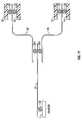
- FIG. 1is an elevation view of module 10 devised in accordance with a preferred embodiment of the present invention.
- module 10includes upper CSP 16 and lower CSP 18 .
- Lower CSP 18is inverted with respect to upper CSP 16 .
- Each of the constituent CSPshas an upper surface 20 and a lower surface 22 and opposite lateral edges 24 and 26 and includes at least one integrated circuit typically surrounded by a plastic body 27 .
- the bodyneed not be plastic, but a large majority of packages in CSP technologies are plastic.
- the present inventionmay be devised to create modules with different size CSPs and that the constituent CSPs may be of different types within the same module 10 .
- one of the constituent CSPsmay be a typical CSP having lateral edges 24 and 26 that have an appreciable height to present a “side” while other constituent CSPs of the same module 10 may be devised in packages that have lateral edges 24 and 26 that are more in the character of an edge rather than a side having appreciable height.
- CSPchip scale packaged integrated circuits
- FIG. 1depicts a CSP of a particular profile known to those in the art, but it should be understood that the figures are exemplary only.
- the inventionmay be employed to advantage in the wide range of CSP configurations available in the art where an array of connective elements is available from at least one major surface.
- the inventionis advantageously employed with CSPs that contain memory circuits, but may be employed to advantage with logic and computing circuits where added capacity without commensurate PWB or other board surface area consumption is desired.
- Typical CSPssuch as, for example, ball-grid-array (“BGA”), micro-ball-grid array, and fine-pitch ball grid array (“FBGA”) packages have an array of connective contacts embodied, for example, as leads, bumps, solder balls, or balls that extend from lower surface 22 of a plastic casing in any of several patterns and pitches. An external portion of the connective contacts is often finished with a ball of solder. Shown in FIG. 1 are contacts 28 along lower surfaces 22 of the illustrated constituent CSPs 16 and 18 . Contacts 28 provide connection to the integrated circuit or circuits within the respective packages. In other embodiments, contacts 28 may be compressed prior to the complete construction of module 10 .
- BGAball-grid-array
- FBGAfine-pitch ball grid array
- Flex circuit 30is shown connecting the constituent CSPs of the module of FIG. 1 .
- Flexible circuit 30has portion 30 A disposed between the depicted CSPs. Portion 30 A presents contacts along each side for connection to CSP 16 and inverted CSP 18 .
- Such an inverted schemeallows electrical connection to each of the depicted CSPs with flex circuit 30 traces having a balanced, equal, or equivalent length. Such connections will be further described with reference to later Figures.
- Each of CSPs 16 and 18has an associated form standard 34 .
- Flex circuit 30is, in this embodiment, wrapped about the lower form standard 34 . While use of a form standard 34 is preferred, other embodiments may not use a form standard.
- the entire flex circuit 30may be flexible or, as those of skill in the art will recognize, a PCB structure made flexible in certain areas to allow conformability around CSPs and rigid in other areas for planarity along CSP surfaces may be employed as an alternative flex circuit in the present invention.
- structures known as rigid-flexmay be employed.
- More than one flex circuitmay be employed to implement the connections between constituent CSPs in a module 10 .
- Another exemplar embodimentuses three flexible circuits, but more or less may be used.
- Each form standard 34 in FIG. 1is disposed along upper planar surface 20 and laterally beyond edges 26 and 24 of body 27 of CSPs 16 and 18 in stacked module 10 .
- Form standard 34is disposed along a surface of a CSP even if literally separated from that surface by adhesive, for example.
- Form standard 34may take many configurations, with examples of embodiments having a downward opening form standard shown in pending U.S. patent application Ser. No. 10/453,398, filed Jun. 3, 2003, a flat form standard, an angular cap, and, as another exemplar, an upward opening form standard shown in pending U.S. patent application Ser. No. 10/845,029, filed May 13, 2004. Both of U.S. patent application Ser. No. 10/453,398 and U.S. patent application Ser. No. 10/845,029 are commonly owned by the assignee of the present invention and are hereby incorporated by reference.
- Module 10exhibits module contacts 38 through which module 10 connects to application environments in a preferred embodiment. Those of skill will recognize that module contacts 38 are not required to connect module 10 to an application environment and other connective strategies may be employed such as, for example, direct pad to pad connection schemes.
- Form standard 34is, in a preferred embodiment, devised from nickel-plated copper to create a mandrel that mitigates thermal accumulation while providing a standard sized form about which flex circuitry is disposed.
- Form standard 34may take other shapes and forms that are coincident with the respective CSP body. It also need not be thermally enhancing although such attributes are preferable.
- the form standard 34allows the invention to be employed with CSPs of varying sizes, while articulating a single set of connective structures useable with the varying sizes of CSPs.
- a single set of connective structuressuch as flex circuits 30 and 32 (or a single flexible circuit in the mode where a single flex is used in place of the flex circuit pair 30 and 32 ) may be devised and used with the form standard 34 method and/or systems disclosed herein to create stacked modules with CSPs having different-sized packages.
- Thiswill allow the same flex circuitry design to be employed to create iterations of a stacked module 10 from constituent CSPs having a first arbitrary dimension X across attribute Y (where Y may be, for example, package width), as well as modules 10 from, constituent CSPs having a second arbitrary dimension X prime across that same attribute Y.
- CSPs of different sizesmay be stacked into modules 10 with the same set of connective structures (i.e. flex circuitry). Further, as those of skill will recognize, mixed sizes of CSPs may be implemented into the same module 10 .
- portions of flex circuits 30 and 32may be attached to form standard 34 by metallic bonds.
- metallic bondsPreferred examples of such metallic bonding of flex circuitry to a form standard are further described in co-pending U.S. patent application Ser. No. 10/828,495, filed Apr. 20, 2004, which is commonly owned by the assignee of the present invention and hereby incorporated by reference.
- Other methods for attaching form standard 34 to flex circuitrymay be employed in the present invention including, for example, a tape or liquid adhesive. If an adhesive is used for the attachment, the adhesive will be thermally conductive.
- Form standard 34 associated with the upper depicted CSP 16 in this embodimentmay improve the thermal performance of module 10 .
- Other embodimentsmay not have a form standard associated with CSP 16 .
- FIG. 2depicts an embodiment without a second form standard 34 .
- FIG. 3depicts a two-level embodiment having a spacer 33 .
- the depicted spacer 33may be employed to enable use of a standard-sized flex circuit 30 and form standard 34 with differently-sized CSPs 18 . While FIG. 3 is not shown to scale, the depicted CSPs are thinner than those depicted in FIG. 1 .
- Spacer 33is preferably a piece of metal or other heat conductive material, and may also act as a heat spreader.
- FIG. 4depicts a two-level embodiment of module 10 having standard 34 associated with lower CSP 18 .
- Form standard 34opens upward relative to CSP 18 .
- the direction “upward”is meant to be with reference to the orientation of the depicted CSP 18 and as those of skill recognize, the side or major surface of CSP 18 having contacts 28 is typically referred to as “lower”.
- Other embodimentsmay employ flat form standards that do not exhibit an opening orientation.
- Module 10may be mounted in many different orientations.
- One preferred form standard 34 for use in embodiments such as that in FIG. 4is the upward opening form standard shown in pending U.S. patent application Ser. No. 10/845,029, filed May 13, 2004, which application has been incorporated by reference.
- Form standard 34is comprised of nickel-plated copper and exhibits two windows identified by references B and C to allow the array of contacts 28 that rise above lower surface 22 of the respective CSP to readily pass through form standard 34 .
- Form standard 34may take other configurations and may, for example, be devised in more than one piece.
- FIG. 5depicts a three-level embodiment of module 10 having two inverted CSPs 16 and 18 .
- the two depicted flex circuits 30are disposed about respective form standards 34 .
- the upper depicted CSP 14is mounted to flex contacts along the upper depicted side of flex 30 .
- the lower depicted CSPs 16 and 18are first assembled into a submodule with their respective flex circuits 30 , and submodule contacts 38 are added to the upper flex circuit 30 .
- Submodule contacts 38may be called “inter-flex” contacts 38 when they are employed as depicted between flex circuits 30 .
- Such inter-flex contactsmay be low-profile contacts having a flattened solder ball or other low profile contacts design such as, for example, a pad with built-up metal plating or solder.
- FIG. 6depicts a four-level embodiment of module 10 that employs three form standards 34 with a form standard 34 associated with each of CSPs 14 , 16 and 18 .
- each level in module 10need not have a form standard but where maximum heat extraction is desired, use of a form standard 34 on the upper depicted CSP 12 is preferred.
- inter-flex contacts 38are used to enable connection between flex circuits 30 associated with CSPs 16 and 18 , as well as between CSPs 14 and 16 .
- FIG. 7depicts a four-level embodiment of module 10 that employs a submodule construction scheme.
- the lower depicted CSPs 18 and 16are preferably constructed as a submodule 5 according to the embodiment in FIG. 1 .
- the flex circuit 30 wrapped about form standard 34 associated with CSP 18may be referred to as a “submodule” flex circuit, when used to connect a stacked submodule of CSPs that will be employed in a larger module.
- Such a submodule 5is inverted in this embodiment, as shown by CSP 18 being depicted above CSP 16 .
- An additional flex circuit 31is depicted wrapped about submodule 5 to enable connection of submodule 5 's submodule contacts 38 A (“inter-flex contacts”) to the operating environment through the lower depicted module contacts 38 .
- the upper two CSPs 12 and 14are also assembled into a submodule which is mounted with submodule contacts 38 B (“inter-flex contacts”) to flex contacts on flex circuit 31 .
- Such use of a flex circuit 31may provide, in this embodiment, a balanced signaling capability by providing equal-length conductive paths to each of the depicted CSPs from the operating environment to which module contacts 38 are meant to connect. Such a balanced signaling scheme is further described with reference to FIGS. 8-11 .
- FIG. 8shows a contact bailout pattern for a portion of a flex circuit according to one preferred embodiment of the present invention.
- the patternis shown for flex contacts on a flex circuit portion between an inverted CSP and a non-inverted CSP, such as portion 30 A depicted in FIG. 1 .
- the tablealternates to show rows of a bailout pattern on both sides of portion 30 A.
- Rows 801show the bailout pattern on the top side of portion 30 A, to which CSP 16 is attached.
- Rows 802show the bailout pattern for the bottom side of portion 30 A, to which CSP 18 is attached in the preferred embodiment depicted in FIG. 1 .
- the bailout pattern depictedis that for a common memory CSP bailout pattern defined by JEDEC for DDR2 DRAMs. Many other types of CSPs may be used. Many of the depicted signals, although given a specific topology in this preferred bailout pattern, may be swapped with another signal of the same type as is needed for different memory allocation schemes or other applications. For example, DQ 0 could be used as DQ 8 or A 4 could be swapped with A 7 to facilitate routing.
- FIG. 9depicts a connection topology for a flex circuit according to one embodiment of the present invention.
- flex circuit 30is shown straightened to better illustrate the signal trace topology.
- a single module contact 38is shown connected to an operating environment 1 , which may be a memory DIMM board or other circuit board or system.
- Flex circuit 30connects module contact 38 with a trace to contacts 28 on upper CSP 16 and lower CSP 18 .
- both contacts 28are connected to the same flex contact pad or to oppositely-disposed and electrically connected contact pads on flex circuit 30 .
- Such a connectionallows signals such as address, data, and strobe signals to be routed to both of the depicted CSPs with the same signal delay.
- This balanced schememay be desired for high-speed operations in which a minimal skew time between signals is critical.
- the depicted topologyminimizes skew time by providing equal length traces, which may also provide more manageable signal reflections on the depicted signal line. Ball swapping is preferably employed to achieve such a balanced connections scheme wherever the bailout topology employed allows substitution of signals.
- the depicted topologymay present any transmission line terminations, such as, for example, on-die-terminations, which may be associated with each the depicted opposing contacts 28 as a lumped impedance to the transmission line (trace).
- FIG. 10depicts a connection topology for another embodiment.
- the depicted trace on flex 30connects module contact 38 to a CSP contact 28 on upper CSP 16 and then to a contact 28 on CSP 18 .
- Other connectionsmay have a shorter connection to CSP 18 .
- Such a connection schemeprovides unequal length traces for the shared signal and is not preferred but may be employed, however, when the bailout topology of CSPs stacked in a particular module 10 requires it.
- FIG. 11depicts a connection topology for a preferred four-level module according to one embodiment of the present invention such as is depicted in FIG. 7 .
- Flex circuit 31connects module contact 38 with a trace to inter-flex contacts 38 A and 38 B, which may be attached to a central flex contact pad or to oppositely-disposed but electrically connected flex contact pads.
- Contacts 38 A and 38 Bconnect to respective pairs of CSP contacts 28 through the depicted traces on flex circuit 30 .
- Such a signal topologyallows equal length signal traces to all four CSPs in the depicted module 10 .
- FIG. 12is a flow chart of a process for making a preferred embodiment such as that depicted in FIG. 1 .
- Step 1201attaches a form standard 34 to CSP 18 . Such attachment is preferably made with heat conductive adhesive.
- Step 1202places CSP 18 onto a flex contact pad array, preferably in the central portion 30 A of flex 30 .
- CSP 18is preferably attached with standard solder reflow techniques.
- Step 1203wraps flex circuit 30 around form standard 34 and attaches or tacks the loose end(s) of flex circuit 30 to form standard 34 . The wrapping is preferably about the opposing curved “forms” depicted at both lateral sides of form standard 34 in FIG. 1 .
- the wrapping in step 1203aligns flex contact pad arrays on each of the depicted wrapped ends for attachment of module contacts 38 , which conform to a desired module footprint on the operating environment.
- the attachment in step 1203is preferably done with adhesive or metallic bonds.
- Step 1204inverts the assembly to place portion 30 A above CSP 18 . This allows placement of CSP 16 on a flex contact array pad on the opposite side of flex circuit 30 from CSP 18 in step 1205 . Step 1205 also reflows to attach CSP 16 to flex circuit 30 . CSP 16 may optionally have a form standard 34 attached before step 1205 . Step 1206 attaches module contacts 38 to a flex contact pad array.
- FIG. 13is a flow chart of one process for making a preferred embodiment such as that depicted in FIG. 7 .
- step 1301first provides a pair of two-level modules such as those depicted in FIG. 1 .
- the pair of modulesare employed as submodules 5 and 6 for assembling the four-level module depicted in FIG. 7 .
- Step 1302paces a first submodule 5 ( FIG. 7 ) onto a long flex circuit 31 and reflows.
- Step 1303wraps long flex circuit 31 around the first module and attaches the opposing ends to form standard 34 of CSP 16 .
- Step 1304inverts the assembly for placement of the second submodule 6 on a contact pad array along the opposite side of flex circuit 31 from submodule 5 .
- Step 1305places and reflows the second submodule 6 .
- Step 1306attaches module contacts 38 to flex circuit 31 .
- FIG. 14depicts a top and bottom view of a flex circuit 30 according to the embodiment depicted in FIG. 1 .
- Top side Tis shown having flex contact pad array 1401 for attachment of attachment of CSP 16 .
- Side Talso has flex contact pad arrays 1402 for attachment of module contacts 38 .
- Bottom side Bhas flex contact pad array 1403 for attachment of CSP 18 .
- the depicted pad arraysare preferably expressed by conductive layers in flex circuit 30 and may be covered by insulative layers.
- Flex circuit 31has a similar topology to that depicted here, but has length needed to wrap about a submodule of two CSPs.
- FIG. 15is an enlarged cross-sectional view of the portion marked A in FIG. 1 .
- flex circuitry 30comprises two conductive layers 40 and 42 separated by intermediate layer 41 .
- the conductive layersare metal such as alloy 110 .
- conductive layer 42may be included in flex circuitry employed in the invention.
- Flex circuits that employ only a single conductive layersuch as, for example, those that employ only a layer such as conductive layer 42 may be readily employed in embodiments of the invention.
- the use of plural conductive layersmay provide, however, advantages and the creation of a distributed capacitance across module 10 intended to reduce noise or bounce effects that can, particularly at higher frequencies, degrade signal integrity, as those of skill in the art will recognize.
- the opposing pair of flex contactsincluding flex contact 44 at the level of conductive layer 42 and flex contact 46 at the level of conductive layer 40 provide contact sites to allow interconnection of CSP contacts 28 through via 48 .
- flex contacts 44are aggregated as the flex contact pad array 1401 depicted in FIG. 14 .
- Flex contacts 46preferably are aggregated as the array 1403 .
- the depicted right-hand portion of conductive layer 42expresses the conductive trace carrying the electrical signal to both contacts 28 .
- Other embodimentsmay not use a via but instead may connect opposing CSP contacts 28 (or module contacts 38 in the case of an embodiment such as that in FIG. 7 ) directly to a particular conductive layer through a window in flexible intermediate layer 41 .
- Such connectionis preferably with a direct connection with a very short length conductor.
- Such a short conductorpresents both contacts as a lumped element with no transmission lines or traces between them. This may be beneficial for presenting both attached contacts 28 as a lumped circuit element or termination to the transmission line trace 44 .
- Other embodimentsmay use a trace to connect flex contacts on opposite sides of flex 30 where the contacts conduct a common signal to CSP contacts 28 that are not directly opposite.
- Such a situationmay be accomplished by using conductive traces 44 of equal or electrically equivalent length. Construction of traces having electrically equivalent length is known in the art. Further, while a two conductive layer flex circuit is shown, other embodiments may use other numbers of layers. Two conductive layers are preferred.
- FIG. 16depicts a circuit module according to an alternative embodiment of the present invention.
- CSP 18is inverted and connected to its operating environment though flex circuit 30 .
- CSP 18may also be interconnected to other components mounted to flex circuit 30 .
- Extra module contacts 38 Epresent additional connections which interconnect any of extra components 161 - 165 to an operating environment using the conductive traces of flex circuit 30 .
- Other embodiments with multiple similarly sized CSPssuch as, for example, multiple memory CSPs, may also have extra module contacts 38 E.
- Such a schemeallows for expansion of circuit board mounting space.
- Such a schemealso allows for mounting of peripheral devices such as surface mount capacitor 161 and surface mount resistor 163 near their associated integrated circuits.
- CSP 18is a microprocessor or other controller and CSPs 162 , 164 , and 165 are supporting integrated circuits such as, for example, memory circuits, amplifiers, and analog-to-digital or digital-to-analog converters.
Landscapes
- Engineering & Computer Science (AREA)
- Microelectronics & Electronic Packaging (AREA)
- Power Engineering (AREA)
- Physics & Mathematics (AREA)
- Condensed Matter Physics & Semiconductors (AREA)
- General Physics & Mathematics (AREA)
- Computer Hardware Design (AREA)
- Combinations Of Printed Boards (AREA)
- Structure Of Printed Boards (AREA)
Abstract
Description
Claims (14)
Priority Applications (2)
| Application Number | Priority Date | Filing Date | Title |
|---|---|---|---|
| US11/039,615US7309914B2 (en) | 2005-01-20 | 2005-01-20 | Inverted CSP stacking system and method |
| US11/926,494US20080079132A1 (en) | 2005-01-20 | 2007-10-29 | Inverted CSP Stacking System and Method |
Applications Claiming Priority (1)
| Application Number | Priority Date | Filing Date | Title |
|---|---|---|---|
| US11/039,615US7309914B2 (en) | 2005-01-20 | 2005-01-20 | Inverted CSP stacking system and method |
Related Child Applications (1)
| Application Number | Title | Priority Date | Filing Date |
|---|---|---|---|
| US11/926,494DivisionUS20080079132A1 (en) | 2005-01-20 | 2007-10-29 | Inverted CSP Stacking System and Method |
Publications (2)
| Publication Number | Publication Date |
|---|---|
| US20060157842A1 US20060157842A1 (en) | 2006-07-20 |
| US7309914B2true US7309914B2 (en) | 2007-12-18 |
Family
ID=36683042
Family Applications (2)
| Application Number | Title | Priority Date | Filing Date |
|---|---|---|---|
| US11/039,615Expired - LifetimeUS7309914B2 (en) | 2005-01-20 | 2005-01-20 | Inverted CSP stacking system and method |
| US11/926,494AbandonedUS20080079132A1 (en) | 2005-01-20 | 2007-10-29 | Inverted CSP Stacking System and Method |
Family Applications After (1)
| Application Number | Title | Priority Date | Filing Date |
|---|---|---|---|
| US11/926,494AbandonedUS20080079132A1 (en) | 2005-01-20 | 2007-10-29 | Inverted CSP Stacking System and Method |
Country Status (1)
| Country | Link |
|---|---|
| US (2) | US7309914B2 (en) |
Cited By (4)
| Publication number | Priority date | Publication date | Assignee | Title |
|---|---|---|---|---|
| US20080157332A1 (en)* | 2006-12-29 | 2008-07-03 | Samsung Electronics Co., Ltd. | Stacked semiconductor packages and methods of manufacturing stacked semiconductor packages |
| US20080203552A1 (en)* | 2005-02-15 | 2008-08-28 | Unisemicon Co., Ltd. | Stacked Package and Method of Fabricating the Same |
| US20080299709A1 (en)* | 2006-08-28 | 2008-12-04 | Micron Technology, Inc. | Metal core foldover package structures |
| US8588017B2 (en) | 2010-10-20 | 2013-11-19 | Samsung Electronics Co., Ltd. | Memory circuits, systems, and modules for performing DRAM refresh operations and methods of operating the same |
Families Citing this family (17)
| Publication number | Priority date | Publication date | Assignee | Title |
|---|---|---|---|---|
| KR100615606B1 (en)* | 2005-03-15 | 2006-08-25 | 삼성전자주식회사 | Memory Modules and How to Place Signal Lines in These Modules |
| DE102005059189B3 (en)* | 2005-12-12 | 2007-03-08 | Infineon Technologies Ag | Arrangement of semiconductor memory devices for module, has conductive tracks connecting contacts of flexible substrate and stacked semiconductor devices |
| US7868440B2 (en) | 2006-08-25 | 2011-01-11 | Micron Technology, Inc. | Packaged microdevices and methods for manufacturing packaged microdevices |
| US7514773B2 (en)* | 2006-08-31 | 2009-04-07 | Intel Corporation | Systems and arrangements for interconnecting integrated circuit dies |
| US7772708B2 (en)* | 2006-08-31 | 2010-08-10 | Intel Corporation | Stacking integrated circuit dies |
| US7697281B2 (en) | 2008-09-05 | 2010-04-13 | Apple Inc. | Handheld computing device |
| US7869206B2 (en) | 2008-09-05 | 2011-01-11 | Apple Inc. | Handheld computing device |
| US8477492B2 (en) | 2010-08-19 | 2013-07-02 | Apple Inc. | Formed PCB |
| US9602914B2 (en) | 2010-08-27 | 2017-03-21 | Apple Inc. | Porting audio using a connector in a small form factor electronic device |
| US8634204B2 (en) | 2010-08-19 | 2014-01-21 | Apple Inc. | Compact folded configuration for integrated circuit packaging |
| US8391010B2 (en) | 2010-08-19 | 2013-03-05 | Apple Inc. | Internal frame optimized for stiffness and heat transfer |
| CN103221896B (en) | 2010-08-19 | 2017-06-09 | 苹果公司 | Portable electric appts |
| US8427379B2 (en) | 2010-08-19 | 2013-04-23 | Apple Inc. | Modular material antenna assembly |
| US8515113B2 (en) | 2010-08-19 | 2013-08-20 | Apple Inc. | Composite microphone boot to optimize sealing and mechanical properties |
| US9287627B2 (en) | 2011-08-31 | 2016-03-15 | Apple Inc. | Customizable antenna feed structure |
| US9406999B2 (en) | 2011-09-23 | 2016-08-02 | Apple Inc. | Methods for manufacturing customized antenna structures |
| CN203225947U (en)* | 2013-03-28 | 2013-10-02 | 富士康(昆山)电脑接插件有限公司 | Printed circuit board assembly |
Citations (274)
| Publication number | Priority date | Publication date | Assignee | Title |
|---|---|---|---|---|
| US3411122A (en) | 1966-01-13 | 1968-11-12 | Ibm | Electrical resistance element and method of fabricating |
| US3438604A (en) | 1966-11-16 | 1969-04-15 | William M Spicer | Retainer clips for temporary wiring |
| US3654394A (en) | 1969-07-08 | 1972-04-04 | Gordon Eng Co | Field effect transistor switch, particularly for multiplexing |
| US3727064A (en) | 1971-03-17 | 1973-04-10 | Monsanto Co | Opto-isolator devices and method for the fabrication thereof |
| US3746934A (en) | 1971-05-06 | 1973-07-17 | Siemens Ag | Stack arrangement of semiconductor chips |
| US3766439A (en) | 1972-01-12 | 1973-10-16 | Gen Electric | Electronic module using flexible printed circuit board with heat sink means |
| US3772776A (en) | 1969-12-03 | 1973-11-20 | Thomas & Betts Corp | Method of interconnecting memory plane boards |
| JPS5029534A (en) | 1973-02-20 | 1975-03-25 | ||
| US3983547A (en) | 1974-06-27 | 1976-09-28 | International Business Machines - Ibm | Three-dimensional bubble device |
| US4079511A (en) | 1976-07-30 | 1978-03-21 | Amp Incorporated | Method for packaging hermetically sealed integrated circuit chips on lead frames |
| US4103318A (en) | 1977-05-06 | 1978-07-25 | Ford Motor Company | Electronic multichip module |
| US4288841A (en) | 1979-09-20 | 1981-09-08 | Bell Telephone Laboratories, Incorporated | Double cavity semiconductor chip carrier |
| US4398235A (en) | 1980-09-11 | 1983-08-09 | General Motors Corporation | Vertical integrated circuit package integration |
| US4406508A (en) | 1981-07-02 | 1983-09-27 | Thomas & Betts Corporation | Dual-in-line package assembly |
| US4437235A (en) | 1980-12-29 | 1984-03-20 | Honeywell Information Systems Inc. | Integrated circuit package |
| US4513368A (en) | 1981-05-22 | 1985-04-23 | Data General Corporation | Digital data processing system having object-based logical memory addressing and self-structuring modular memory |
| JPS60254762A (en) | 1984-05-31 | 1985-12-16 | Fujitsu Ltd | Semiconductor device package |
| US4587596A (en) | 1984-04-09 | 1986-05-06 | Amp Incorporated | High density mother/daughter circuit board connector |
| US4645944A (en) | 1983-09-05 | 1987-02-24 | Matsushita Electric Industrial Co., Ltd. | MOS register for selecting among various data inputs |
| US4696525A (en) | 1985-12-13 | 1987-09-29 | Amp Incorporated | Socket for stacking integrated circuit packages |
| JPS62230027A (en) | 1986-03-31 | 1987-10-08 | Matsushita Electric Ind Co Ltd | Manufacture of semiconductor device |
| US4712129A (en) | 1983-12-12 | 1987-12-08 | Texas Instruments Incorporated | Integrated circuit device with textured bar cover |
| US4722691A (en) | 1986-02-03 | 1988-02-02 | General Motors Corporation | Header assembly for a printed circuit board |
| US4733461A (en) | 1984-12-28 | 1988-03-29 | Micro Co., Ltd. | Method of stacking printed circuit boards |
| JPS63153849A (en) | 1986-12-17 | 1988-06-27 | Nec Corp | Semiconductor device |
| US4758875A (en) | 1981-04-30 | 1988-07-19 | Hitachi, Ltd. | Resin encapsulated semiconductor device |
| US4763188A (en) | 1986-08-08 | 1988-08-09 | Thomas Johnson | Packaging system for multiple semiconductor devices |
| US4821007A (en) | 1987-02-06 | 1989-04-11 | Tektronix, Inc. | Strip line circuit component and method of manufacture |
| US4823234A (en) | 1985-08-16 | 1989-04-18 | Dai-Ichi Seiko Co., Ltd. | Semiconductor device and its manufacture |
| US4833568A (en) | 1988-01-29 | 1989-05-23 | Berhold G Mark | Three-dimensional circuit component assembly and method corresponding thereto |
| US4839717A (en) | 1986-12-19 | 1989-06-13 | Fairchild Semiconductor Corporation | Ceramic package for high frequency semiconductor devices |
| US4862249A (en) | 1987-04-17 | 1989-08-29 | Xoc Devices, Inc. | Packaging system for stacking integrated circuits |
| US4884237A (en) | 1984-03-28 | 1989-11-28 | International Business Machines Corporation | Stacked double density memory module using industry standard memory chips |
| US4891789A (en) | 1988-03-03 | 1990-01-02 | Bull Hn Information Systems, Inc. | Surface mounted multilayer memory printed circuit board |
| US4911643A (en) | 1988-10-11 | 1990-03-27 | Beta Phase, Inc. | High density and high signal integrity connector |
| US4953060A (en) | 1989-05-05 | 1990-08-28 | Ncr Corporation | Stackable integrated circuit chip package with improved heat removal |
| US4956694A (en) | 1988-11-04 | 1990-09-11 | Dense-Pac Microsystems, Inc. | Integrated circuit chip stacking |
| US4983533A (en) | 1987-10-28 | 1991-01-08 | Irvine Sensors Corporation | High-density electronic modules - process and product |
| US4985703A (en) | 1988-02-03 | 1991-01-15 | Nec Corporation | Analog multiplexer |
| US5012323A (en) | 1989-11-20 | 1991-04-30 | Micron Technology, Inc. | Double-die semiconductor package having a back-bonded die and a face-bonded die interconnected on a single leadframe |
| EP0426303A2 (en) | 1989-10-31 | 1991-05-08 | International Business Machines Corporation | A soldering method |
| US5016138A (en) | 1987-10-27 | 1991-05-14 | Woodman John K | Three dimensional integrated circuit package |
| US5034350A (en) | 1987-09-23 | 1991-07-23 | Sgs Thomson Microelectronics S.R.L. | Semiconductor device package with dies mounted on both sides of the central pad of a metal frame |
| US5041015A (en) | 1990-03-30 | 1991-08-20 | Cal Flex, Inc. | Electrical jumper assembly |
| US5041902A (en) | 1989-12-14 | 1991-08-20 | Motorola, Inc. | Molded electronic package with compression structures |
| US5057903A (en) | 1989-07-17 | 1991-10-15 | Microelectronics And Computer Technology Corporation | Thermal heat sink encapsulated integrated circuit |
| US5064782A (en) | 1989-04-17 | 1991-11-12 | Sumitomo Electric Industries, Ltd. | Method of adhesively and hermetically sealing a semiconductor package lid by scrubbing |
| US5068708A (en) | 1989-10-02 | 1991-11-26 | Advanced Micro Devices, Inc. | Ground plane for plastic encapsulated integrated circuit die packages |
| US5081067A (en) | 1989-02-10 | 1992-01-14 | Fujitsu Limited | Ceramic package type semiconductor device and method of assembling the same |
| US5099393A (en) | 1991-03-25 | 1992-03-24 | International Business Machines Corporation | Electronic package for high density applications |
| US5104820A (en) | 1989-07-07 | 1992-04-14 | Irvine Sensors Corporation | Method of fabricating electronic circuitry unit containing stacked IC layers having lead rerouting |
| US5117282A (en) | 1990-10-29 | 1992-05-26 | Harris Corporation | Stacked configuration for integrated circuit devices |
| US5122862A (en) | 1989-03-15 | 1992-06-16 | Ngk Insulators, Ltd. | Ceramic lid for sealing semiconductor element and method of manufacturing the same |
| JPH04209562A (en) | 1990-12-06 | 1992-07-30 | Fujitsu Ltd | Module structure of semiconductor package |
| US5138434A (en) | 1991-01-22 | 1992-08-11 | Micron Technology, Inc. | Packaging for semiconductor logic devices |
| US5138430A (en) | 1991-06-06 | 1992-08-11 | International Business Machines Corporation | High performance versatile thermally enhanced IC chip mounting |
| US5159535A (en) | 1987-03-11 | 1992-10-27 | International Business Machines Corporation | Method and apparatus for mounting a flexible film semiconductor chip carrier on a circuitized substrate |
| US5159434A (en) | 1990-02-01 | 1992-10-27 | Hitachi, Ltd. | Semiconductor device having a particular chip pad structure |
| US5158912A (en) | 1991-04-09 | 1992-10-27 | Digital Equipment Corporation | Integral heatsink semiconductor package |
| US5168926A (en) | 1991-09-25 | 1992-12-08 | Intel Corporation | Heat sink design integrating interface material |
| US5198888A (en) | 1987-12-28 | 1993-03-30 | Hitachi, Ltd. | Semiconductor stacked device |
| US5198965A (en) | 1991-12-18 | 1993-03-30 | International Business Machines Corporation | Free form packaging of specific functions within a computer system |
| US5214307A (en) | 1991-07-08 | 1993-05-25 | Micron Technology, Inc. | Lead frame for semiconductor devices having improved adhesive bond line control |
| US5219794A (en) | 1991-03-14 | 1993-06-15 | Hitachi, Ltd. | Semiconductor integrated circuit device and method of fabricating same |
| US5222014A (en) | 1992-03-02 | 1993-06-22 | Motorola, Inc. | Three-dimensional multi-chip pad array carrier |
| US5224023A (en) | 1992-02-10 | 1993-06-29 | Smith Gary W | Foldable electronic assembly module |
| US5229916A (en) | 1992-03-04 | 1993-07-20 | International Business Machines Corporation | Chip edge interconnect overlay element |
| US5239198A (en) | 1989-09-06 | 1993-08-24 | Motorola, Inc. | Overmolded semiconductor device having solder ball and edge lead connective structure |
| US5241454A (en) | 1992-01-22 | 1993-08-31 | International Business Machines Corporation | Mutlilayered flexible circuit package |
| US5240588A (en) | 1991-08-27 | 1993-08-31 | Nec Corporation | Method for electroplating the lead pins of a semiconductor device pin grid array package |
| US5243133A (en) | 1992-02-18 | 1993-09-07 | International Business Machines, Inc. | Ceramic chip carrier with lead frame or edge clip |
| US5247423A (en) | 1992-05-26 | 1993-09-21 | Motorola, Inc. | Stacking three dimensional leadless multi-chip module and method for making the same |
| US5252857A (en) | 1991-08-05 | 1993-10-12 | International Business Machines Corporation | Stacked DCA memory chips |
| US5252855A (en) | 1990-10-25 | 1993-10-12 | Mitsubishi Denki Kabushiki Kaisha | Lead frame having an anodic oxide film coating |
| US5259770A (en) | 1992-03-19 | 1993-11-09 | Amp Incorporated | Impedance controlled elastomeric connector |
| US5261068A (en) | 1990-05-25 | 1993-11-09 | Dell Usa L.P. | Dual path memory retrieval system for an interleaved dynamic RAM memory unit |
| US5262927A (en) | 1992-02-07 | 1993-11-16 | Lsi Logic Corporation | Partially-molded, PCB chip carrier package |
| US5276418A (en) | 1988-11-16 | 1994-01-04 | Motorola, Inc. | Flexible substrate electronic assembly |
| US5279029A (en) | 1990-08-01 | 1994-01-18 | Staktek Corporation | Ultra high density integrated circuit packages method |
| US5281852A (en) | 1991-12-10 | 1994-01-25 | Normington Peter J C | Semiconductor device including stacked die |
| US5289062A (en) | 1991-03-18 | 1994-02-22 | Quality Semiconductor, Inc. | Fast transmission gate switch |
| US5311401A (en) | 1991-07-09 | 1994-05-10 | Hughes Aircraft Company | Stacked chip assembly and manufacturing method therefor |
| US5313097A (en) | 1992-11-16 | 1994-05-17 | International Business Machines, Corp. | High density memory module |
| US5343075A (en) | 1991-06-29 | 1994-08-30 | Sony Corporation | Composite stacked semiconductor device with contact plates |
| US5347428A (en) | 1992-12-03 | 1994-09-13 | Irvine Sensors Corporation | Module comprising IC memory stack dedicated to and structurally combined with an IC microprocessor chip |
| US5357478A (en) | 1990-10-05 | 1994-10-18 | Mitsubishi Denki Kabushiki Kaisha | Semiconductor integrated circuit device including a plurality of cell array blocks |
| US5361228A (en) | 1992-04-30 | 1994-11-01 | Fuji Photo Film Co., Ltd. | IC memory card system having a common data and address bus |
| US5375041A (en) | 1992-12-02 | 1994-12-20 | Intel Corporation | Ra-tab array bump tab tape based I.C. package |
| US5377077A (en) | 1990-08-01 | 1994-12-27 | Staktek Corporation | Ultra high density integrated circuit packages method and apparatus |
| US5386341A (en) | 1993-11-01 | 1995-01-31 | Motorola, Inc. | Flexible substrate folded in a U-shape with a rigidizer plate located in the notch of the U-shape |
| US5394303A (en) | 1992-09-11 | 1995-02-28 | Kabushiki Kaisha Toshiba | Semiconductor device |
| US5394010A (en) | 1991-03-13 | 1995-02-28 | Kabushiki Kaisha Toshiba | Semiconductor assembly having laminated semiconductor devices |
| US5397916A (en) | 1991-12-10 | 1995-03-14 | Normington; Peter J. C. | Semiconductor device including stacked die |
| US5402006A (en) | 1992-11-10 | 1995-03-28 | Texas Instruments Incorporated | Semiconductor device with enhanced adhesion between heat spreader and leads and plastic mold compound |
| US5428190A (en) | 1993-07-02 | 1995-06-27 | Sheldahl, Inc. | Rigid-flex board with anisotropic interconnect and method of manufacture |
| US5438224A (en) | 1992-04-23 | 1995-08-01 | Motorola, Inc. | Integrated circuit package having a face-to-face IC chip arrangement |
| US5446620A (en) | 1990-08-01 | 1995-08-29 | Staktek Corporation | Ultra high density integrated circuit packages |
| US5448511A (en) | 1994-06-01 | 1995-09-05 | Storage Technology Corporation | Memory stack with an integrated interconnect and mounting structure |
| US5455740A (en) | 1994-03-07 | 1995-10-03 | Staktek Corporation | Bus communication system for stacked high density integrated circuit packages |
| US5477082A (en) | 1994-01-11 | 1995-12-19 | Exponential Technology, Inc. | Bi-planar multi-chip module |
| US5475920A (en) | 1990-08-01 | 1995-12-19 | Burns; Carmen D. | Method of assembling ultra high density integrated circuit packages |
| US5484959A (en) | 1992-12-11 | 1996-01-16 | Staktek Corporation | High density lead-on-package fabrication method and apparatus |
| US5499160A (en) | 1990-08-01 | 1996-03-12 | Staktek Corporation | High density integrated circuit module with snap-on rail assemblies |
| US5502333A (en) | 1994-03-30 | 1996-03-26 | International Business Machines Corporation | Semiconductor stack structures and fabrication/sparing methods utilizing programmable spare circuit |
| US5514907A (en) | 1995-03-21 | 1996-05-07 | Simple Technology Incorporated | Apparatus for stacking semiconductor chips |
| US5523619A (en) | 1993-11-03 | 1996-06-04 | International Business Machines Corporation | High density memory structure |
| US5523695A (en) | 1994-08-26 | 1996-06-04 | Vlsi Technology, Inc. | Universal test socket for exposing the active surface of an integrated circuit in a die-down package |
| US5541812A (en) | 1995-05-22 | 1996-07-30 | Burns; Carmen D. | Bus communication system for stacked high density integrated circuit packages having an intermediate lead frame |
| US5572065A (en) | 1992-06-26 | 1996-11-05 | Staktek Corporation | Hermetically sealed ceramic integrated circuit heat dissipating package |
| US5588205A (en) | 1995-01-24 | 1996-12-31 | Staktek Corporation | Method of manufacturing a high density integrated circuit module having complex electrical interconnect rails |
| US5592364A (en) | 1995-01-24 | 1997-01-07 | Staktek Corporation | High density integrated circuit module with complex electrical interconnect rails |
| US5594275A (en) | 1993-11-18 | 1997-01-14 | Samsung Electronics Co., Ltd. | J-leaded semiconductor package having a plurality of stacked ball grid array packages |
| US5612570A (en) | 1995-04-13 | 1997-03-18 | Dense-Pac Microsystems, Inc. | Chip stack and method of making same |
| US5642055A (en) | 1990-02-14 | 1997-06-24 | Particle Interconnect, Inc. | Electrical interconnect using particle enhanced joining of metal surfaces |
| US5644161A (en) | 1993-03-29 | 1997-07-01 | Staktek Corporation | Ultra-high density warp-resistant memory module |
| US5646446A (en) | 1995-12-22 | 1997-07-08 | Fairchild Space And Defense Corporation | Three-dimensional flexible assembly of integrated circuits |
| US5654877A (en) | 1991-08-15 | 1997-08-05 | Staktek Corporation | Lead-on-chip integrated circuit apparatus |
| US5657537A (en) | 1995-05-30 | 1997-08-19 | General Electric Company | Method for fabricating a stack of two dimensional circuit modules |
| US5677569A (en) | 1994-10-27 | 1997-10-14 | Samsung Electronics Co., Ltd. | Semiconductor multi-package stack |
| US5729894A (en) | 1992-07-21 | 1998-03-24 | Lsi Logic Corporation | Method of assembling ball bump grid array semiconductor packages |
| US5744827A (en) | 1995-11-28 | 1998-04-28 | Samsung Electronics Co., Ltd. | Three dimensional stack package device having exposed coupling lead portions and vertical interconnection elements |
| US5751553A (en) | 1992-09-16 | 1998-05-12 | Clayton; James E. | Thin multichip module including a connector frame socket having first and second apertures |
| US5763296A (en) | 1991-11-21 | 1998-06-09 | Sgs-Thomson Microelectronics S.R.L. | Method for fabricating an electronic device structure with studs locating lead frame on backing plate |
| US5764497A (en) | 1995-11-13 | 1998-06-09 | Minolta Co, Ltd. | Circuit board connection method and connection structure |
| US5778522A (en) | 1996-05-20 | 1998-07-14 | Staktek Corporation | Method of manufacturing a high density integrated circuit module with complex electrical interconnect rails having electrical interconnect strain relief |
| US5783464A (en) | 1992-06-26 | 1998-07-21 | Staktek Corporation | Method of forming a hermetically sealed circuit lead-on package |
| US5789815A (en) | 1996-04-23 | 1998-08-04 | Motorola, Inc. | Three dimensional semiconductor package having flexible appendages |
| US5801437A (en) | 1993-03-29 | 1998-09-01 | Staktek Corporation | Three-dimensional warp-resistant integrated circuit module method and apparatus |
| US5801439A (en) | 1994-04-20 | 1998-09-01 | Fujitsu Limited | Semiconductor device and semiconductor device unit for a stack arrangement |
| US5805422A (en) | 1994-09-21 | 1998-09-08 | Nec Corporation | Semiconductor package with flexible board and method of fabricating the same |
| US5835988A (en) | 1996-03-27 | 1998-11-10 | Mitsubishi Denki Kabushiki Kaisha | Packed semiconductor device with wrap around external leads |
| US5841721A (en) | 1994-09-03 | 1998-11-24 | Samsung Electronics Co., Ltd | Multi-block erase and verification circuit in a nonvolatile semiconductor memory device and a method thereof |
| US5869353A (en) | 1997-11-17 | 1999-02-09 | Dense-Pac Microsystems, Inc. | Modular panel stacking process |
| US5895970A (en) | 1997-05-02 | 1999-04-20 | Nec Corporation | Semiconductor package having semiconductor element, mounting structure of semiconductor package mounted on circuit board, and method of assembling semiconductor package |
| US5899705A (en) | 1997-11-20 | 1999-05-04 | Akram; Salman | Stacked leads-over chip multi-chip module |
| US5917709A (en) | 1997-06-16 | 1999-06-29 | Eastman Kodak Company | Multiple circuit board assembly having an interconnect mechanism that includes a flex connector |
| US5922061A (en) | 1995-10-20 | 1999-07-13 | Iq Systems | Methods and apparatus for implementing high speed data communications |
| US5925934A (en) | 1995-10-28 | 1999-07-20 | Institute Of Microelectronics | Low cost and highly reliable chip-sized package |
| US5926369A (en) | 1998-01-22 | 1999-07-20 | International Business Machines Corporation | Vertically integrated multi-chip circuit package with heat-sink support |
| US5949657A (en) | 1997-12-01 | 1999-09-07 | Karabatsos; Chris | Bottom or top jumpered foldable electronic assembly |
| US5953215A (en) | 1997-12-01 | 1999-09-14 | Karabatsos; Chris | Apparatus and method for improving computer memory speed and capacity |
| US5959839A (en) | 1997-01-02 | 1999-09-28 | At&T Corp | Apparatus for heat removal using a flexible backplane |
| US5963427A (en) | 1997-12-11 | 1999-10-05 | Sun Microsystems, Inc. | Multi-chip module with flexible circuit board |
| US5973392A (en)* | 1997-04-02 | 1999-10-26 | Nec Corporation | Stacked carrier three-dimensional memory module and semiconductor device using the same |
| US5973395A (en) | 1996-04-30 | 1999-10-26 | Yamaichi Electronics Co., Ltd. | IC package having a single wiring sheet with a lead pattern disposed thereon |
| US5995370A (en) | 1997-09-01 | 1999-11-30 | Sharp Kabushiki Kaisha | Heat-sinking arrangement for circuit elements |
| US6002167A (en) | 1995-09-22 | 1999-12-14 | Hitachi Cable, Ltd. | Semiconductor device having lead on chip structure |
| US6002589A (en) | 1997-07-21 | 1999-12-14 | Rambus Inc. | Integrated circuit package for coupling to a printed circuit board |
| US6014316A (en) | 1997-06-13 | 2000-01-11 | Irvine Sensors Corporation | IC stack utilizing BGA contacts |
| US6025642A (en) | 1995-08-17 | 2000-02-15 | Staktek Corporation | Ultra high density integrated circuit packages |
| US6028365A (en) | 1998-03-30 | 2000-02-22 | Micron Technology, Inc. | Integrated circuit package and method of fabrication |
| US6028352A (en) | 1997-06-13 | 2000-02-22 | Irvine Sensors Corporation | IC stack utilizing secondary leadframes |
| US6034878A (en) | 1996-12-16 | 2000-03-07 | Hitachi, Ltd. | Source-clock-synchronized memory system and memory unit |
| US6040624A (en) | 1997-10-02 | 2000-03-21 | Motorola, Inc. | Semiconductor device package and method |
| US6072233A (en) | 1998-05-04 | 2000-06-06 | Micron Technology, Inc. | Stackable ball grid array package |
| US6084294A (en) | 1998-08-26 | 2000-07-04 | Mitsubishi Denki Kabushiki Kaisha | Semiconductor device comprising stacked semiconductor elements |
| US6084293A (en) | 1997-07-25 | 2000-07-04 | Oki Electric Industry Co., Ltd. | Stacked semiconductor device |
| US6097087A (en) | 1997-10-31 | 2000-08-01 | Micron Technology, Inc. | Semiconductor package including flex circuit, interconnects and dense array external contacts |
| US6121676A (en) | 1996-12-13 | 2000-09-19 | Tessera, Inc. | Stacked microelectronic assembly and method therefor |
| JP2000307029A (en) | 1999-04-26 | 2000-11-02 | Oki Electric Ind Co Ltd | Semiconductor device and semiconductor module |
| US6153928A (en)* | 1996-05-17 | 2000-11-28 | Hyuandai Electronics Industries Co., Ltd. | Substrate for semiconductor package, fabrication method thereof, and stacked-type semiconductor package using the substrate |
| US6157541A (en) | 1997-12-30 | 2000-12-05 | Siemens Aktiengesellschaft | Stack arrangement for two semiconductor memory chips and printed board for accepting a plurality of such stack arrangements |
| US6172874B1 (en) | 1998-04-06 | 2001-01-09 | Silicon Graphics, Inc. | System for stacking of integrated circuit packages |
| US6178093B1 (en) | 1996-06-28 | 2001-01-23 | International Business Machines Corporation | Information handling system with circuit assembly having holes filled with filler material |
| US6187652B1 (en) | 1998-09-14 | 2001-02-13 | Fujitsu Limited | Method of fabrication of multiple-layer high density substrate |
| JP2001077294A (en) | 1999-09-02 | 2001-03-23 | Nec Corp | Semiconductor device |
| US6208521B1 (en) | 1997-05-19 | 2001-03-27 | Nitto Denko Corporation | Film carrier and laminate type mounting structure using same |
| US6205654B1 (en) | 1992-12-11 | 2001-03-27 | Staktek Group L.P. | Method of manufacturing a surface mount package |
| JP2001085592A (en) | 1999-09-17 | 2001-03-30 | Seiko Epson Corp | Semiconductor device and its manufacturing method, circuit board, and electronic equipment |
| US6222737B1 (en) | 1999-04-23 | 2001-04-24 | Dense-Pac Microsystems, Inc. | Universal package and method of forming the same |
| US6225688B1 (en) | 1997-12-11 | 2001-05-01 | Tessera, Inc. | Stacked microelectronic assembly and method therefor |
| US6233650B1 (en) | 1998-04-01 | 2001-05-15 | Intel Corporation | Using FET switches for large memory arrays |
| US6234820B1 (en) | 1997-07-21 | 2001-05-22 | Rambus Inc. | Method and apparatus for joining printed circuit boards |
| US6262476B1 (en) | 1998-07-27 | 2001-07-17 | Siemens Aktiengesellschaft | Composite member composed of at least two integrated circuits and method for the manufacture of a composite member composed of at least two integrated circuits |
| US6262895B1 (en) | 2000-01-13 | 2001-07-17 | John A. Forthun | Stackable chip package with flex carrier |
| US6266252B1 (en) | 1997-12-01 | 2001-07-24 | Chris Karabatsos | Apparatus and method for terminating a computer memory bus |
| US6265660B1 (en) | 1997-07-09 | 2001-07-24 | Micron Technology, Inc. | Package stack via bottom leaded plastic (BLP) packaging |
| US20010013423A1 (en) | 1996-10-31 | 2001-08-16 | Hormazdyar M. Dalal | Flip chip attach on flexible circuit carrier using chip with metallic cap on solder |
| US6281577B1 (en) | 1996-06-28 | 2001-08-28 | Pac Tech-Packaging Technologies Gmbh | Chips arranged in plurality of planes and electrically connected to one another |
| US6285560B1 (en) | 1999-09-20 | 2001-09-04 | Texas Instruments Incorporated | Method for increasing device reliability by selectively depopulating solder balls from a foot print of a ball grid array (BGA) package, and device so modified |
| US6300679B1 (en) | 1998-06-01 | 2001-10-09 | Semiconductor Components Industries, Llc | Flexible substrate for packaging a semiconductor component |
| US6303981B1 (en) | 1999-09-01 | 2001-10-16 | Micron Technology, Inc. | Semiconductor package having stacked dice and leadframes and method of fabrication |
| US6310392B1 (en) | 1998-12-28 | 2001-10-30 | Staktek Group, L.P. | Stacked micro ball grid array packages |
| US20010035572A1 (en) | 1999-05-05 | 2001-11-01 | Isaak Harlan R. | Stackable flex circuit chip package and method of making same |
| US6313998B1 (en) | 1999-04-02 | 2001-11-06 | Legacy Electronics, Inc. | Circuit board assembly having a three dimensional array of integrated circuit packages |
| US6316825B1 (en) | 1998-05-15 | 2001-11-13 | Hyundai Electronics Industries Co., Ltd. | Chip stack package utilizing a connecting hole to improve electrical connection between leadframes |
| US20010040793A1 (en) | 2000-02-01 | 2001-11-15 | Tetsuya Inaba | Electronic device and method of producing the same |
| US6323060B1 (en) | 1999-05-05 | 2001-11-27 | Dense-Pac Microsystems, Inc. | Stackable flex circuit IC package and method of making same |
| JP2001332683A (en) | 2000-05-19 | 2001-11-30 | Nec Corp | Laminated semiconductor device and manufacturing method thereof |
| US6336262B1 (en) | 1996-10-31 | 2002-01-08 | International Business Machines Corporation | Process of forming a capacitor with multi-level interconnection technology |
| US20020006032A1 (en) | 2000-05-23 | 2002-01-17 | Chris Karabatsos | Low-profile registered DIMM |
| US20020030995A1 (en) | 2000-08-07 | 2002-03-14 | Masao Shoji | Headlight |
| US6376769B1 (en) | 1999-05-18 | 2002-04-23 | Amerasia International Technology, Inc. | High-density electronic package, and method for making same |
| US6392162B1 (en) | 2000-11-10 | 2002-05-21 | Chris Karabatsos | Double-sided flexible jumper assembly and method of manufacture |
| US20020076919A1 (en) | 1998-11-13 | 2002-06-20 | Peters Michael G. | Composite interposer and method for producing a composite interposer |
| US6410857B1 (en) | 2001-03-01 | 2002-06-25 | Lockheed Martin Corporation | Signal cross-over interconnect for a double-sided circuit card assembly |
| US6426560B1 (en) | 1999-08-06 | 2002-07-30 | Hitachi, Ltd. | Semiconductor device and memory module |
| US20020101261A1 (en) | 2001-02-01 | 2002-08-01 | Chris Karabatsos | Tri-directional, high-speed bus switch |
| US6433418B1 (en) | 1998-07-24 | 2002-08-13 | Fujitsu Limited | Apparatus for a vertically accumulable semiconductor device with external leads secured by a positioning mechanism |
| US6444921B1 (en) | 2000-02-03 | 2002-09-03 | Fujitsu Limited | Reduced stress and zero stress interposers for integrated-circuit chips, multichip substrates, and the like |
| US6444490B2 (en) | 1998-06-26 | 2002-09-03 | International Business Machines Corporation | Micro-flex technology in semiconductor packages |
| US6446158B1 (en) | 1999-05-17 | 2002-09-03 | Chris Karabatsos | Memory system using FET switches to select memory banks |
| US6449159B1 (en) | 2000-05-03 | 2002-09-10 | Rambus Inc. | Semiconductor module with imbedded heat spreader |
| US6452826B1 (en) | 2000-10-26 | 2002-09-17 | Samsung Electronics Co., Ltd. | Memory module system |
| US20020139577A1 (en) | 2001-03-27 | 2002-10-03 | Miller Charles A. | In-street integrated circuit wafer via |
| US6462412B2 (en) | 2000-01-18 | 2002-10-08 | Sony Corporation | Foldable, flexible laminate type semiconductor apparatus with reinforcing and heat-radiating plates |
| US6465893B1 (en) | 1990-09-24 | 2002-10-15 | Tessera, Inc. | Stacked chip assembly |
| US20020164838A1 (en) | 2001-05-02 | 2002-11-07 | Moon Ow Chee | Flexible ball grid array chip scale packages and methods of fabrication |
| US6486544B1 (en) | 1998-09-09 | 2002-11-26 | Seiko Epson Corporation | Semiconductor device and method manufacturing the same, circuit board, and electronic instrument |
| US6489178B2 (en) | 2000-01-26 | 2002-12-03 | Texas Instruments Incorporated | Method of fabricating a molded package for micromechanical devices |
| US6489687B1 (en) | 1999-10-01 | 2002-12-03 | Seiko Epson Corporation | Semiconductor device and method of manufacturing the same, manufacturing device, circuit board, and electronic equipment |
| US20020180022A1 (en) | 1999-10-20 | 2002-12-05 | Seiko Epson Corporation | Semiconductor device |
| US6492718B2 (en) | 1999-12-20 | 2002-12-10 | Kabushiki Kaisha Toshiba | Stacked semiconductor device and semiconductor system |
| US6509639B1 (en) | 2001-07-27 | 2003-01-21 | Charles W. C. Lin | Three-dimensional stacked semiconductor package |
| US20030016710A1 (en) | 2001-07-19 | 2003-01-23 | Satoshi Komoto | Semiconductor laser device including light receiving element for receiving monitoring laser beam |
| JP2003037246A (en) | 2002-05-29 | 2003-02-07 | Hitachi Ltd | Electronic components and electronic component modules |
| US6528870B2 (en) | 2000-01-28 | 2003-03-04 | Kabushiki Kaisha Toshiba | Semiconductor device having a plurality of stacked wiring boards |
| US20030042590A1 (en)* | 2001-08-30 | 2003-03-06 | Bernd Goller | Electronic component and process for producing the electronic component |
| US20030049886A1 (en) | 2001-09-07 | 2003-03-13 | Salmon Peter C. | Electronic system modules and method of fabrication |
| JP2003086761A (en) | 2001-09-14 | 2003-03-20 | Casio Comput Co Ltd | Semiconductor device and manufacturing method thereof |
| JP2003088760A (en) | 2001-09-19 | 2003-03-25 | Tosoh Corp | Catalyst for trimerizing ethylene and method for trimerizing ethylene using the catalyst |
| US6552910B1 (en) | 2000-06-28 | 2003-04-22 | Micron Technology, Inc. | Stacked-die assemblies with a plurality of microelectronic devices and methods of manufacture |
| US20030081392A1 (en) | 2001-10-26 | 2003-05-01 | Staktek Group, L.P. | Integrated circuit stacking system and method |
| WO2003037053A1 (en) | 2001-10-26 | 2003-05-01 | Staktek Group, L.P. | Chip scale stacking system and method |
| US6560117B2 (en) | 2000-06-28 | 2003-05-06 | Micron Technology, Inc. | Packaged microelectronic die assemblies and methods of manufacture |
| US6572387B2 (en) | 1999-09-24 | 2003-06-03 | Staktek Group, L.P. | Flexible circuit connector for stacked chip module |
| US20030109078A1 (en) | 1996-12-03 | 2003-06-12 | Yoshikazu Takahashi | Semiconductor device, method for manufacturing the same, and method for mounting the same |
| US20030107118A1 (en) | 2001-10-09 | 2003-06-12 | Tessera, Inc. | Stacked packages |
| US6588095B2 (en) | 2001-04-27 | 2003-07-08 | Hewlett-Packard Development Company, Lp. | Method of processing a device by electrophoresis coating |
| US6590282B1 (en) | 2002-04-12 | 2003-07-08 | Industrial Technology Research Institute | Stacked semiconductor package formed on a substrate and method for fabrication |
| US6600222B1 (en) | 2002-07-17 | 2003-07-29 | Intel Corporation | Stacked microelectronic packages |
| US6614664B2 (en) | 2000-10-24 | 2003-09-02 | Samsung Electronics Co., Ltd. | Memory module having series-connected printed circuit boards |
| US20030168725A1 (en) | 1996-12-13 | 2003-09-11 | Tessera, Inc. | Methods of making microelectronic assemblies including folded substrates |
| US6620651B2 (en) | 2001-10-23 | 2003-09-16 | National Starch And Chemical Investment Holding Corporation | Adhesive wafers for die attach application |
| US6627984B2 (en) | 2001-07-24 | 2003-09-30 | Dense-Pac Microsystems, Inc. | Chip stack with differing chip package types |
| JP2003309246A (en) | 2003-05-12 | 2003-10-31 | Oki Electric Ind Co Ltd | Semiconductor module |
| JP2003309247A (en) | 2003-05-12 | 2003-10-31 | Oki Electric Ind Co Ltd | Semiconductor module |
| US6657134B2 (en) | 2001-11-30 | 2003-12-02 | Honeywell International Inc. | Stacked ball grid array |
| JP2003347503A (en) | 2002-05-30 | 2003-12-05 | Hitachi Ltd | Semiconductor device and method of manufacturing the same, and semiconductor mounting structure |
| JP2003347475A (en) | 2003-05-12 | 2003-12-05 | Oki Electric Ind Co Ltd | Semiconductor |
| US6660561B2 (en) | 2000-06-15 | 2003-12-09 | Dpac Technologies Corp. | Method of assembling a stackable integrated circuit chip |
| US20040000708A1 (en) | 2001-10-26 | 2004-01-01 | Staktek Group, L.P. | Memory expansion and chip scale stacking system and method |
| US6677670B2 (en) | 2000-04-25 | 2004-01-13 | Seiko Epson Corporation | Semiconductor device |
| US6683377B1 (en) | 2000-05-30 | 2004-01-27 | Amkor Technology, Inc. | Multi-stacked memory package |
| US20040021211A1 (en) | 2002-08-05 | 2004-02-05 | Tessera, Inc. | Microelectronic adaptors, assemblies and methods |
| US6690584B2 (en) | 2000-08-14 | 2004-02-10 | Fujitsu Limited | Information-processing device having a crossbar-board connected to back panels on different sides |
| US20040031972A1 (en) | 2001-10-09 | 2004-02-19 | Tessera, Inc. | Stacked packages |
| US20040045159A1 (en) | 1996-12-13 | 2004-03-11 | Tessera, Inc. | Electrical connection with inwardly deformable contacts |
| US6707684B1 (en) | 2001-04-02 | 2004-03-16 | Advanced Micro Devices, Inc. | Method and apparatus for direct connection between two integrated circuits via a connector |
| US6709893B2 (en) | 1998-05-11 | 2004-03-23 | Micron Technology, Inc. | Interconnections for a semiconductor device and method for forming same |
| US20040065963A1 (en) | 2002-09-17 | 2004-04-08 | Chippac, Inc. | Semiconductor multi-package module having wire bond interconnect between stacked packages and having electrical shield |
| US20040075991A1 (en) | 1999-08-11 | 2004-04-22 | Tessera. Inc. | Vapor phase connection techniques |
| US20040099938A1 (en) | 2002-09-11 | 2004-05-27 | Tessera, Inc. | Assemblies having stacked semiconductor chips and methods of making same |
| US20040104470A1 (en) | 2002-08-16 | 2004-06-03 | Tessera, Inc. | Microelectronic packages with self-aligning features |
| US20040113253A1 (en)* | 2002-10-08 | 2004-06-17 | Chippac, Inc. | Semiconductor stacked multi-package module having inverted second package |
| US20040115866A1 (en) | 2002-09-06 | 2004-06-17 | Tessera, Inc. | Methods of making microelectronic packages including folded substrates |
| US6768660B2 (en) | 2001-01-08 | 2004-07-27 | Samsung Electronics Co. Ltd. | Multi-chip memory devices and modules including independent control of memory chips |
| US20040150107A1 (en) | 2002-12-31 | 2004-08-05 | Cha Ki Bon | Stack package and fabricating method thereof |
| US20040157352A1 (en) | 2000-11-13 | 2004-08-12 | Kim Soo Kil | Method for forming thin film and method for fabricating liquid crystal display using the same |
| US6781240B2 (en) | 2001-06-26 | 2004-08-24 | Samsung Electronics Co., Ltd. | Semiconductor package with semiconductor chips stacked therein and method of making the package |
| US6803651B1 (en) | 2002-01-09 | 2004-10-12 | Bridge Semiconductor Corporation | Optoelectronic semiconductor package device |
| US6812567B2 (en) | 2002-11-28 | 2004-11-02 | Samsung Electronics Co., Ltd. | Semiconductor package and package stack made thereof |
| US20040217471A1 (en) | 2003-02-27 | 2004-11-04 | Tessera, Inc. | Component and assemblies with ends offset downwardly |
| US20040238931A1 (en) | 2003-05-30 | 2004-12-02 | Tessera, Inc. | Assemblies having stacked semiconductor chips and methods of making same |
| US20040245617A1 (en) | 2003-05-06 | 2004-12-09 | Tessera, Inc. | Dense multichip module |
| US6833984B1 (en) | 2000-05-03 | 2004-12-21 | Rambus, Inc. | Semiconductor module with serial bus connection to multiple dies |
| US20050018495A1 (en) | 2004-01-29 | 2005-01-27 | Netlist, Inc. | Arrangement of integrated circuits in a memory module |
| US6849949B1 (en) | 1999-09-27 | 2005-02-01 | Samsung Electronics Co., Ltd. | Thin stacked package |
| US20050035440A1 (en) | 2001-08-22 | 2005-02-17 | Tessera, Inc. | Stacked chip assembly with stiffening layer |
| US20050040508A1 (en) | 2003-08-22 | 2005-02-24 | Jong-Joo Lee | Area array type package stack and manufacturing method thereof |
| US6876074B2 (en) | 2001-10-10 | 2005-04-05 | Samsung Electronics Co., Ltd. | Stack package using flexible double wiring substrate |
| US6884653B2 (en) | 2001-03-21 | 2005-04-26 | Micron Technology, Inc. | Folded interposer |
| US6891729B2 (en) | 2001-09-10 | 2005-05-10 | Samsung Electronics Co., Ltd. | Memory module |
| US20050133897A1 (en) | 2003-12-17 | 2005-06-23 | Baek Joong-Hyun | Stack package with improved heat radiation and module having the stack package mounted thereon |
Family Cites Families (2)
| Publication number | Priority date | Publication date | Assignee | Title |
|---|---|---|---|---|
| JPS57146941A (en)* | 1981-03-06 | 1982-09-10 | Aisin Warner Ltd | Oil pressure controller for automatic speed changer |
| IT1310046B1 (en)* | 1999-03-18 | 2002-02-05 | Armi San Marco S R L | SAFETY DEVICE FOR RIVOLTELLE. |
- 2005
- 2005-01-20USUS11/039,615patent/US7309914B2/ennot_activeExpired - Lifetime
- 2007
- 2007-10-29USUS11/926,494patent/US20080079132A1/ennot_activeAbandoned
Patent Citations (306)
| Publication number | Priority date | Publication date | Assignee | Title |
|---|---|---|---|---|
| US3411122A (en) | 1966-01-13 | 1968-11-12 | Ibm | Electrical resistance element and method of fabricating |
| US3438604A (en) | 1966-11-16 | 1969-04-15 | William M Spicer | Retainer clips for temporary wiring |
| US3654394A (en) | 1969-07-08 | 1972-04-04 | Gordon Eng Co | Field effect transistor switch, particularly for multiplexing |
| US3772776A (en) | 1969-12-03 | 1973-11-20 | Thomas & Betts Corp | Method of interconnecting memory plane boards |
| US3727064A (en) | 1971-03-17 | 1973-04-10 | Monsanto Co | Opto-isolator devices and method for the fabrication thereof |
| US3746934A (en) | 1971-05-06 | 1973-07-17 | Siemens Ag | Stack arrangement of semiconductor chips |
| US3766439A (en) | 1972-01-12 | 1973-10-16 | Gen Electric | Electronic module using flexible printed circuit board with heat sink means |
| JPS5029534A (en) | 1973-02-20 | 1975-03-25 | ||
| US3983547A (en) | 1974-06-27 | 1976-09-28 | International Business Machines - Ibm | Three-dimensional bubble device |
| US4079511A (en) | 1976-07-30 | 1978-03-21 | Amp Incorporated | Method for packaging hermetically sealed integrated circuit chips on lead frames |
| US4103318A (en) | 1977-05-06 | 1978-07-25 | Ford Motor Company | Electronic multichip module |
| US4288841A (en) | 1979-09-20 | 1981-09-08 | Bell Telephone Laboratories, Incorporated | Double cavity semiconductor chip carrier |
| US4398235A (en) | 1980-09-11 | 1983-08-09 | General Motors Corporation | Vertical integrated circuit package integration |
| US4437235A (en) | 1980-12-29 | 1984-03-20 | Honeywell Information Systems Inc. | Integrated circuit package |
| US4758875A (en) | 1981-04-30 | 1988-07-19 | Hitachi, Ltd. | Resin encapsulated semiconductor device |
| US4513368A (en) | 1981-05-22 | 1985-04-23 | Data General Corporation | Digital data processing system having object-based logical memory addressing and self-structuring modular memory |
| US4406508A (en) | 1981-07-02 | 1983-09-27 | Thomas & Betts Corporation | Dual-in-line package assembly |
| US4645944A (en) | 1983-09-05 | 1987-02-24 | Matsushita Electric Industrial Co., Ltd. | MOS register for selecting among various data inputs |
| US4712129A (en) | 1983-12-12 | 1987-12-08 | Texas Instruments Incorporated | Integrated circuit device with textured bar cover |
| US4884237A (en) | 1984-03-28 | 1989-11-28 | International Business Machines Corporation | Stacked double density memory module using industry standard memory chips |
| US4587596A (en) | 1984-04-09 | 1986-05-06 | Amp Incorporated | High density mother/daughter circuit board connector |
| JPS60254762A (en) | 1984-05-31 | 1985-12-16 | Fujitsu Ltd | Semiconductor device package |
| US4733461A (en) | 1984-12-28 | 1988-03-29 | Micro Co., Ltd. | Method of stacking printed circuit boards |
| US4823234A (en) | 1985-08-16 | 1989-04-18 | Dai-Ichi Seiko Co., Ltd. | Semiconductor device and its manufacture |
| US4696525A (en) | 1985-12-13 | 1987-09-29 | Amp Incorporated | Socket for stacking integrated circuit packages |
| US4722691A (en) | 1986-02-03 | 1988-02-02 | General Motors Corporation | Header assembly for a printed circuit board |
| JPS62230027A (en) | 1986-03-31 | 1987-10-08 | Matsushita Electric Ind Co Ltd | Manufacture of semiconductor device |
| US4763188A (en) | 1986-08-08 | 1988-08-09 | Thomas Johnson | Packaging system for multiple semiconductor devices |
| JPS63153849A (en) | 1986-12-17 | 1988-06-27 | Nec Corp | Semiconductor device |
| US4839717A (en) | 1986-12-19 | 1989-06-13 | Fairchild Semiconductor Corporation | Ceramic package for high frequency semiconductor devices |
| US4821007A (en) | 1987-02-06 | 1989-04-11 | Tektronix, Inc. | Strip line circuit component and method of manufacture |
| US5159535A (en) | 1987-03-11 | 1992-10-27 | International Business Machines Corporation | Method and apparatus for mounting a flexible film semiconductor chip carrier on a circuitized substrate |
| US4862249A (en) | 1987-04-17 | 1989-08-29 | Xoc Devices, Inc. | Packaging system for stacking integrated circuits |
| US5034350A (en) | 1987-09-23 | 1991-07-23 | Sgs Thomson Microelectronics S.R.L. | Semiconductor device package with dies mounted on both sides of the central pad of a metal frame |
| US5016138A (en) | 1987-10-27 | 1991-05-14 | Woodman John K | Three dimensional integrated circuit package |
| US4983533A (en) | 1987-10-28 | 1991-01-08 | Irvine Sensors Corporation | High-density electronic modules - process and product |
| US5198888A (en) | 1987-12-28 | 1993-03-30 | Hitachi, Ltd. | Semiconductor stacked device |
| US4833568A (en) | 1988-01-29 | 1989-05-23 | Berhold G Mark | Three-dimensional circuit component assembly and method corresponding thereto |
| US4985703A (en) | 1988-02-03 | 1991-01-15 | Nec Corporation | Analog multiplexer |
| US4891789A (en) | 1988-03-03 | 1990-01-02 | Bull Hn Information Systems, Inc. | Surface mounted multilayer memory printed circuit board |
| US4911643A (en) | 1988-10-11 | 1990-03-27 | Beta Phase, Inc. | High density and high signal integrity connector |
| US4956694A (en) | 1988-11-04 | 1990-09-11 | Dense-Pac Microsystems, Inc. | Integrated circuit chip stacking |
| US5276418A (en) | 1988-11-16 | 1994-01-04 | Motorola, Inc. | Flexible substrate electronic assembly |
| US5081067A (en) | 1989-02-10 | 1992-01-14 | Fujitsu Limited | Ceramic package type semiconductor device and method of assembling the same |
| US5122862A (en) | 1989-03-15 | 1992-06-16 | Ngk Insulators, Ltd. | Ceramic lid for sealing semiconductor element and method of manufacturing the same |
| US5064782A (en) | 1989-04-17 | 1991-11-12 | Sumitomo Electric Industries, Ltd. | Method of adhesively and hermetically sealing a semiconductor package lid by scrubbing |
| US4953060A (en) | 1989-05-05 | 1990-08-28 | Ncr Corporation | Stackable integrated circuit chip package with improved heat removal |
| US5104820A (en) | 1989-07-07 | 1992-04-14 | Irvine Sensors Corporation | Method of fabricating electronic circuitry unit containing stacked IC layers having lead rerouting |
| US5057903A (en) | 1989-07-17 | 1991-10-15 | Microelectronics And Computer Technology Corporation | Thermal heat sink encapsulated integrated circuit |
| US5239198A (en) | 1989-09-06 | 1993-08-24 | Motorola, Inc. | Overmolded semiconductor device having solder ball and edge lead connective structure |
| US5068708A (en) | 1989-10-02 | 1991-11-26 | Advanced Micro Devices, Inc. | Ground plane for plastic encapsulated integrated circuit die packages |
| EP0426303A2 (en) | 1989-10-31 | 1991-05-08 | International Business Machines Corporation | A soldering method |
| US5012323A (en) | 1989-11-20 | 1991-04-30 | Micron Technology, Inc. | Double-die semiconductor package having a back-bonded die and a face-bonded die interconnected on a single leadframe |
| US5041902A (en) | 1989-12-14 | 1991-08-20 | Motorola, Inc. | Molded electronic package with compression structures |
| US5159434A (en) | 1990-02-01 | 1992-10-27 | Hitachi, Ltd. | Semiconductor device having a particular chip pad structure |
| US5642055A (en) | 1990-02-14 | 1997-06-24 | Particle Interconnect, Inc. | Electrical interconnect using particle enhanced joining of metal surfaces |
| US5041015A (en) | 1990-03-30 | 1991-08-20 | Cal Flex, Inc. | Electrical jumper assembly |
| US5261068A (en) | 1990-05-25 | 1993-11-09 | Dell Usa L.P. | Dual path memory retrieval system for an interleaved dynamic RAM memory unit |
| US5377077A (en) | 1990-08-01 | 1994-12-27 | Staktek Corporation | Ultra high density integrated circuit packages method and apparatus |
| US5279029A (en) | 1990-08-01 | 1994-01-18 | Staktek Corporation | Ultra high density integrated circuit packages method |
| US5420751A (en) | 1990-08-01 | 1995-05-30 | Staktek Corporation | Ultra high density modular integrated circuit package |
| US5446620A (en) | 1990-08-01 | 1995-08-29 | Staktek Corporation | Ultra high density integrated circuit packages |
| US5566051A (en) | 1990-08-01 | 1996-10-15 | Staktek Corporation | Ultra high density integrated circuit packages method and apparatus |
| US5561591A (en) | 1990-08-01 | 1996-10-01 | Staktek Corporation | Multi-signal rail assembly with impedance control for a three-dimensional high density integrated circuit package |
| US5543664A (en) | 1990-08-01 | 1996-08-06 | Staktek Corporation | Ultra high density integrated circuit package |
| US5499160A (en) | 1990-08-01 | 1996-03-12 | Staktek Corporation | High density integrated circuit module with snap-on rail assemblies |
| US5475920A (en) | 1990-08-01 | 1995-12-19 | Burns; Carmen D. | Method of assembling ultra high density integrated circuit packages |
| US6465893B1 (en) | 1990-09-24 | 2002-10-15 | Tessera, Inc. | Stacked chip assembly |
| US5357478A (en) | 1990-10-05 | 1994-10-18 | Mitsubishi Denki Kabushiki Kaisha | Semiconductor integrated circuit device including a plurality of cell array blocks |
| US5252855A (en) | 1990-10-25 | 1993-10-12 | Mitsubishi Denki Kabushiki Kaisha | Lead frame having an anodic oxide film coating |
| US5117282A (en) | 1990-10-29 | 1992-05-26 | Harris Corporation | Stacked configuration for integrated circuit devices |
| JPH04209562A (en) | 1990-12-06 | 1992-07-30 | Fujitsu Ltd | Module structure of semiconductor package |
| US5138434A (en) | 1991-01-22 | 1992-08-11 | Micron Technology, Inc. | Packaging for semiconductor logic devices |
| US5394010A (en) | 1991-03-13 | 1995-02-28 | Kabushiki Kaisha Toshiba | Semiconductor assembly having laminated semiconductor devices |
| US5219794A (en) | 1991-03-14 | 1993-06-15 | Hitachi, Ltd. | Semiconductor integrated circuit device and method of fabricating same |
| US5289062A (en) | 1991-03-18 | 1994-02-22 | Quality Semiconductor, Inc. | Fast transmission gate switch |
| US5099393A (en) | 1991-03-25 | 1992-03-24 | International Business Machines Corporation | Electronic package for high density applications |
| US5158912A (en) | 1991-04-09 | 1992-10-27 | Digital Equipment Corporation | Integral heatsink semiconductor package |
| US5138430A (en) | 1991-06-06 | 1992-08-11 | International Business Machines Corporation | High performance versatile thermally enhanced IC chip mounting |
| US5343075A (en) | 1991-06-29 | 1994-08-30 | Sony Corporation | Composite stacked semiconductor device with contact plates |
| US5214307A (en) | 1991-07-08 | 1993-05-25 | Micron Technology, Inc. | Lead frame for semiconductor devices having improved adhesive bond line control |
| US5311401A (en) | 1991-07-09 | 1994-05-10 | Hughes Aircraft Company | Stacked chip assembly and manufacturing method therefor |
| US5252857A (en) | 1991-08-05 | 1993-10-12 | International Business Machines Corporation | Stacked DCA memory chips |
| US5654877A (en) | 1991-08-15 | 1997-08-05 | Staktek Corporation | Lead-on-chip integrated circuit apparatus |
| US5240588A (en) | 1991-08-27 | 1993-08-31 | Nec Corporation | Method for electroplating the lead pins of a semiconductor device pin grid array package |
| US5168926A (en) | 1991-09-25 | 1992-12-08 | Intel Corporation | Heat sink design integrating interface material |
| US5763296A (en) | 1991-11-21 | 1998-06-09 | Sgs-Thomson Microelectronics S.R.L. | Method for fabricating an electronic device structure with studs locating lead frame on backing plate |
| US5397916A (en) | 1991-12-10 | 1995-03-14 | Normington; Peter J. C. | Semiconductor device including stacked die |
| US5281852A (en) | 1991-12-10 | 1994-01-25 | Normington Peter J C | Semiconductor device including stacked die |
| US5198965A (en) | 1991-12-18 | 1993-03-30 | International Business Machines Corporation | Free form packaging of specific functions within a computer system |
| US5241454A (en) | 1992-01-22 | 1993-08-31 | International Business Machines Corporation | Mutlilayered flexible circuit package |
| US5262927A (en) | 1992-02-07 | 1993-11-16 | Lsi Logic Corporation | Partially-molded, PCB chip carrier package |
| US5224023A (en) | 1992-02-10 | 1993-06-29 | Smith Gary W | Foldable electronic assembly module |
| US5243133A (en) | 1992-02-18 | 1993-09-07 | International Business Machines, Inc. | Ceramic chip carrier with lead frame or edge clip |
| US5222014A (en) | 1992-03-02 | 1993-06-22 | Motorola, Inc. | Three-dimensional multi-chip pad array carrier |
| US5229916A (en) | 1992-03-04 | 1993-07-20 | International Business Machines Corporation | Chip edge interconnect overlay element |
| US5259770A (en) | 1992-03-19 | 1993-11-09 | Amp Incorporated | Impedance controlled elastomeric connector |
| US5438224A (en) | 1992-04-23 | 1995-08-01 | Motorola, Inc. | Integrated circuit package having a face-to-face IC chip arrangement |
| US5361228A (en) | 1992-04-30 | 1994-11-01 | Fuji Photo Film Co., Ltd. | IC memory card system having a common data and address bus |
| US5247423A (en) | 1992-05-26 | 1993-09-21 | Motorola, Inc. | Stacking three dimensional leadless multi-chip module and method for making the same |
| US5783464A (en) | 1992-06-26 | 1998-07-21 | Staktek Corporation | Method of forming a hermetically sealed circuit lead-on package |
| US5804870A (en) | 1992-06-26 | 1998-09-08 | Staktek Corporation | Hermetically sealed integrated circuit lead-on package configuration |
| US5572065A (en) | 1992-06-26 | 1996-11-05 | Staktek Corporation | Hermetically sealed ceramic integrated circuit heat dissipating package |
| US5729894A (en) | 1992-07-21 | 1998-03-24 | Lsi Logic Corporation | Method of assembling ball bump grid array semiconductor packages |
| US5394303A (en) | 1992-09-11 | 1995-02-28 | Kabushiki Kaisha Toshiba | Semiconductor device |
| US5751553A (en) | 1992-09-16 | 1998-05-12 | Clayton; James E. | Thin multichip module including a connector frame socket having first and second apertures |
| US5402006A (en) | 1992-11-10 | 1995-03-28 | Texas Instruments Incorporated | Semiconductor device with enhanced adhesion between heat spreader and leads and plastic mold compound |
| US5313097A (en) | 1992-11-16 | 1994-05-17 | International Business Machines, Corp. | High density memory module |
| US5375041A (en) | 1992-12-02 | 1994-12-20 | Intel Corporation | Ra-tab array bump tab tape based I.C. package |
| US5347428A (en) | 1992-12-03 | 1994-09-13 | Irvine Sensors Corporation | Module comprising IC memory stack dedicated to and structurally combined with an IC microprocessor chip |
| US5484959A (en) | 1992-12-11 | 1996-01-16 | Staktek Corporation | High density lead-on-package fabrication method and apparatus |
| US6919626B2 (en) | 1992-12-11 | 2005-07-19 | Staktek Group L.P. | High density integrated circuit module |
| US5631193A (en) | 1992-12-11 | 1997-05-20 | Staktek Corporation | High density lead-on-package fabrication method |
| US6205654B1 (en) | 1992-12-11 | 2001-03-27 | Staktek Group L.P. | Method of manufacturing a surface mount package |
| US5644161A (en) | 1993-03-29 | 1997-07-01 | Staktek Corporation | Ultra-high density warp-resistant memory module |
| US5828125A (en) | 1993-03-29 | 1998-10-27 | Staktek Corporation | Ultra-high density warp-resistant memory module |
| US5801437A (en) | 1993-03-29 | 1998-09-01 | Staktek Corporation | Three-dimensional warp-resistant integrated circuit module method and apparatus |
| US5428190A (en) | 1993-07-02 | 1995-06-27 | Sheldahl, Inc. | Rigid-flex board with anisotropic interconnect and method of manufacture |
| US5386341A (en) | 1993-11-01 | 1995-01-31 | Motorola, Inc. | Flexible substrate folded in a U-shape with a rigidizer plate located in the notch of the U-shape |
| US5523619A (en) | 1993-11-03 | 1996-06-04 | International Business Machines Corporation | High density memory structure |
| US5594275A (en) | 1993-11-18 | 1997-01-14 | Samsung Electronics Co., Ltd. | J-leaded semiconductor package having a plurality of stacked ball grid array packages |
| US5477082A (en) | 1994-01-11 | 1995-12-19 | Exponential Technology, Inc. | Bi-planar multi-chip module |
| US5455740A (en) | 1994-03-07 | 1995-10-03 | Staktek Corporation | Bus communication system for stacked high density integrated circuit packages |
| US5479318A (en) | 1994-03-07 | 1995-12-26 | Staktek Corporation | Bus communication system for stacked high density integrated circuit packages with trifurcated distal lead ends |
| US5493476A (en) | 1994-03-07 | 1996-02-20 | Staktek Corporation | Bus communication system for stacked high density integrated circuit packages with bifurcated distal lead ends |
| US5502333A (en) | 1994-03-30 | 1996-03-26 | International Business Machines Corporation | Semiconductor stack structures and fabrication/sparing methods utilizing programmable spare circuit |
| US5801439A (en) | 1994-04-20 | 1998-09-01 | Fujitsu Limited | Semiconductor device and semiconductor device unit for a stack arrangement |
| US5448511A (en) | 1994-06-01 | 1995-09-05 | Storage Technology Corporation | Memory stack with an integrated interconnect and mounting structure |
| US5523695A (en) | 1994-08-26 | 1996-06-04 | Vlsi Technology, Inc. | Universal test socket for exposing the active surface of an integrated circuit in a die-down package |
| US5841721A (en) | 1994-09-03 | 1998-11-24 | Samsung Electronics Co., Ltd | Multi-block erase and verification circuit in a nonvolatile semiconductor memory device and a method thereof |
| US5805422A (en) | 1994-09-21 | 1998-09-08 | Nec Corporation | Semiconductor package with flexible board and method of fabricating the same |
| US5677569A (en) | 1994-10-27 | 1997-10-14 | Samsung Electronics Co., Ltd. | Semiconductor multi-package stack |
| US5592364A (en) | 1995-01-24 | 1997-01-07 | Staktek Corporation | High density integrated circuit module with complex electrical interconnect rails |
| US5588205A (en) | 1995-01-24 | 1996-12-31 | Staktek Corporation | Method of manufacturing a high density integrated circuit module having complex electrical interconnect rails |
| US5514907A (en) | 1995-03-21 | 1996-05-07 | Simple Technology Incorporated | Apparatus for stacking semiconductor chips |
| US5612570A (en) | 1995-04-13 | 1997-03-18 | Dense-Pac Microsystems, Inc. | Chip stack and method of making same |
| US5541812A (en) | 1995-05-22 | 1996-07-30 | Burns; Carmen D. | Bus communication system for stacked high density integrated circuit packages having an intermediate lead frame |
| US5657537A (en) | 1995-05-30 | 1997-08-19 | General Electric Company | Method for fabricating a stack of two dimensional circuit modules |
| US6025642A (en) | 1995-08-17 | 2000-02-15 | Staktek Corporation | Ultra high density integrated circuit packages |
| US6002167A (en) | 1995-09-22 | 1999-12-14 | Hitachi Cable, Ltd. | Semiconductor device having lead on chip structure |
| US5922061A (en) | 1995-10-20 | 1999-07-13 | Iq Systems | Methods and apparatus for implementing high speed data communications |
| US5925934A (en) | 1995-10-28 | 1999-07-20 | Institute Of Microelectronics | Low cost and highly reliable chip-sized package |
| US5764497A (en) | 1995-11-13 | 1998-06-09 | Minolta Co, Ltd. | Circuit board connection method and connection structure |
| US5744827A (en) | 1995-11-28 | 1998-04-28 | Samsung Electronics Co., Ltd. | Three dimensional stack package device having exposed coupling lead portions and vertical interconnection elements |
| US5646446A (en) | 1995-12-22 | 1997-07-08 | Fairchild Space And Defense Corporation | Three-dimensional flexible assembly of integrated circuits |
| US5776797A (en) | 1995-12-22 | 1998-07-07 | Fairchild Space And Defense Corporation | Three-dimensional flexible assembly of integrated circuits |
| US5835988A (en) | 1996-03-27 | 1998-11-10 | Mitsubishi Denki Kabushiki Kaisha | Packed semiconductor device with wrap around external leads |
| US5789815A (en) | 1996-04-23 | 1998-08-04 | Motorola, Inc. | Three dimensional semiconductor package having flexible appendages |
| US5973395A (en) | 1996-04-30 | 1999-10-26 | Yamaichi Electronics Co., Ltd. | IC package having a single wiring sheet with a lead pattern disposed thereon |
| US6153928A (en)* | 1996-05-17 | 2000-11-28 | Hyuandai Electronics Industries Co., Ltd. | Substrate for semiconductor package, fabrication method thereof, and stacked-type semiconductor package using the substrate |
| US6288907B1 (en) | 1996-05-20 | 2001-09-11 | Staktek Group, L.P. | High density integrated circuit module with complex electrical interconnect rails having electrical interconnect strain relief |
| US5778522A (en) | 1996-05-20 | 1998-07-14 | Staktek Corporation | Method of manufacturing a high density integrated circuit module with complex electrical interconnect rails having electrical interconnect strain relief |
| US6178093B1 (en) | 1996-06-28 | 2001-01-23 | International Business Machines Corporation | Information handling system with circuit assembly having holes filled with filler material |
| US6281577B1 (en) | 1996-06-28 | 2001-08-28 | Pac Tech-Packaging Technologies Gmbh | Chips arranged in plurality of planes and electrically connected to one another |
| US20010013423A1 (en) | 1996-10-31 | 2001-08-16 | Hormazdyar M. Dalal | Flip chip attach on flexible circuit carrier using chip with metallic cap on solder |
| US6336262B1 (en) | 1996-10-31 | 2002-01-08 | International Business Machines Corporation | Process of forming a capacitor with multi-level interconnection technology |
| US20030109078A1 (en) | 1996-12-03 | 2003-06-12 | Yoshikazu Takahashi | Semiconductor device, method for manufacturing the same, and method for mounting the same |
| US20040045159A1 (en) | 1996-12-13 | 2004-03-11 | Tessera, Inc. | Electrical connection with inwardly deformable contacts |
| US20010006252A1 (en) | 1996-12-13 | 2001-07-05 | Young Kim | Stacked microelectronic assembly and method therefor |
| US20030168725A1 (en) | 1996-12-13 | 2003-09-11 | Tessera, Inc. | Methods of making microelectronic assemblies including folded substrates |
| US6121676A (en) | 1996-12-13 | 2000-09-19 | Tessera, Inc. | Stacked microelectronic assembly and method therefor |
| US6699730B2 (en) | 1996-12-13 | 2004-03-02 | Tessers, Inc. | Stacked microelectronic assembly and method therefor |
| US6034878A (en) | 1996-12-16 | 2000-03-07 | Hitachi, Ltd. | Source-clock-synchronized memory system and memory unit |
| US5959839A (en) | 1997-01-02 | 1999-09-28 | At&T Corp | Apparatus for heat removal using a flexible backplane |
| US5973392A (en)* | 1997-04-02 | 1999-10-26 | Nec Corporation | Stacked carrier three-dimensional memory module and semiconductor device using the same |
| US5895970A (en) | 1997-05-02 | 1999-04-20 | Nec Corporation | Semiconductor package having semiconductor element, mounting structure of semiconductor package mounted on circuit board, and method of assembling semiconductor package |
| US6208521B1 (en) | 1997-05-19 | 2001-03-27 | Nitto Denko Corporation | Film carrier and laminate type mounting structure using same |
| US6014316A (en) | 1997-06-13 | 2000-01-11 | Irvine Sensors Corporation | IC stack utilizing BGA contacts |
| US6028352A (en) | 1997-06-13 | 2000-02-22 | Irvine Sensors Corporation | IC stack utilizing secondary leadframes |
| US5917709A (en) | 1997-06-16 | 1999-06-29 | Eastman Kodak Company | Multiple circuit board assembly having an interconnect mechanism that includes a flex connector |
| US6265660B1 (en) | 1997-07-09 | 2001-07-24 | Micron Technology, Inc. | Package stack via bottom leaded plastic (BLP) packaging |
| US6002589A (en) | 1997-07-21 | 1999-12-14 | Rambus Inc. | Integrated circuit package for coupling to a printed circuit board |
| US6234820B1 (en) | 1997-07-21 | 2001-05-22 | Rambus Inc. | Method and apparatus for joining printed circuit boards |
| US6084293A (en) | 1997-07-25 | 2000-07-04 | Oki Electric Industry Co., Ltd. | Stacked semiconductor device |
| US5995370A (en) | 1997-09-01 | 1999-11-30 | Sharp Kabushiki Kaisha | Heat-sinking arrangement for circuit elements |
| US6040624A (en) | 1997-10-02 | 2000-03-21 | Motorola, Inc. | Semiconductor device package and method |
| US6368896B2 (en) | 1997-10-31 | 2002-04-09 | Micron Technology, Inc. | Method of wafer level chip scale packaging |
| US6465877B1 (en) | 1997-10-31 | 2002-10-15 | Micron Technology, Inc. | Semiconductor package including flex circuit, interconnects and dense array external contacts |
| US6097087A (en) | 1997-10-31 | 2000-08-01 | Micron Technology, Inc. | Semiconductor package including flex circuit, interconnects and dense array external contacts |
| US5869353A (en) | 1997-11-17 | 1999-02-09 | Dense-Pac Microsystems, Inc. | Modular panel stacking process |
| US5899705A (en) | 1997-11-20 | 1999-05-04 | Akram; Salman | Stacked leads-over chip multi-chip module |
| US5953215A (en) | 1997-12-01 | 1999-09-14 | Karabatsos; Chris | Apparatus and method for improving computer memory speed and capacity |
| US6266252B1 (en) | 1997-12-01 | 2001-07-24 | Chris Karabatsos | Apparatus and method for terminating a computer memory bus |
| US5949657A (en) | 1997-12-01 | 1999-09-07 | Karabatsos; Chris | Bottom or top jumpered foldable electronic assembly |
| US6225688B1 (en) | 1997-12-11 | 2001-05-01 | Tessera, Inc. | Stacked microelectronic assembly and method therefor |
| US5963427A (en) | 1997-12-11 | 1999-10-05 | Sun Microsystems, Inc. | Multi-chip module with flexible circuit board |
| US6157541A (en) | 1997-12-30 | 2000-12-05 | Siemens Aktiengesellschaft | Stack arrangement for two semiconductor memory chips and printed board for accepting a plurality of such stack arrangements |
| US5926369A (en) | 1998-01-22 | 1999-07-20 | International Business Machines Corporation | Vertically integrated multi-chip circuit package with heat-sink support |
| US6165817A (en) | 1998-03-30 | 2000-12-26 | Micron Technology, Inc. | Method of bonding a flexible polymer tape to a substrate to reduce stresses on the electrical connections |
| US6028365A (en) | 1998-03-30 | 2000-02-22 | Micron Technology, Inc. | Integrated circuit package and method of fabrication |
| US6233650B1 (en) | 1998-04-01 | 2001-05-15 | Intel Corporation | Using FET switches for large memory arrays |
| US6172874B1 (en) | 1998-04-06 | 2001-01-09 | Silicon Graphics, Inc. | System for stacking of integrated circuit packages |
| US6072233A (en) | 1998-05-04 | 2000-06-06 | Micron Technology, Inc. | Stackable ball grid array package |
| US6709893B2 (en) | 1998-05-11 | 2004-03-23 | Micron Technology, Inc. | Interconnections for a semiconductor device and method for forming same |
| US6316825B1 (en) | 1998-05-15 | 2001-11-13 | Hyundai Electronics Industries Co., Ltd. | Chip stack package utilizing a connecting hole to improve electrical connection between leadframes |
| US6300679B1 (en) | 1998-06-01 | 2001-10-09 | Semiconductor Components Industries, Llc | Flexible substrate for packaging a semiconductor component |
| US6444490B2 (en) | 1998-06-26 | 2002-09-03 | International Business Machines Corporation | Micro-flex technology in semiconductor packages |
| US6433418B1 (en) | 1998-07-24 | 2002-08-13 | Fujitsu Limited | Apparatus for a vertically accumulable semiconductor device with external leads secured by a positioning mechanism |
| US6262476B1 (en) | 1998-07-27 | 2001-07-17 | Siemens Aktiengesellschaft | Composite member composed of at least two integrated circuits and method for the manufacture of a composite member composed of at least two integrated circuits |
| US6084294A (en) | 1998-08-26 | 2000-07-04 | Mitsubishi Denki Kabushiki Kaisha | Semiconductor device comprising stacked semiconductor elements |
| US6486544B1 (en) | 1998-09-09 | 2002-11-26 | Seiko Epson Corporation | Semiconductor device and method manufacturing the same, circuit board, and electronic instrument |
| US6187652B1 (en) | 1998-09-14 | 2001-02-13 | Fujitsu Limited | Method of fabrication of multiple-layer high density substrate |
| US20020076919A1 (en) | 1998-11-13 | 2002-06-20 | Peters Michael G. | Composite interposer and method for producing a composite interposer |
| US6310392B1 (en) | 1998-12-28 | 2001-10-30 | Staktek Group, L.P. | Stacked micro ball grid array packages |
| US6313998B1 (en) | 1999-04-02 | 2001-11-06 | Legacy Electronics, Inc. | Circuit board assembly having a three dimensional array of integrated circuit packages |
| US6222737B1 (en) | 1999-04-23 | 2001-04-24 | Dense-Pac Microsystems, Inc. | Universal package and method of forming the same |
| US6360433B1 (en) | 1999-04-23 | 2002-03-26 | Andrew C. Ross | Universal package and method of forming the same |
| JP2000307029A (en) | 1999-04-26 | 2000-11-02 | Oki Electric Ind Co Ltd | Semiconductor device and semiconductor module |
| US6329708B1 (en) | 1999-04-26 | 2001-12-11 | Oki Electric Industry Co. Ltd. | Micro ball grid array semiconductor device and semiconductor module |
| US6426549B1 (en) | 1999-05-05 | 2002-07-30 | Harlan R. Isaak | Stackable flex circuit IC package and method of making same |
| US6514793B2 (en) | 1999-05-05 | 2003-02-04 | Dpac Technologies Corp. | Stackable flex circuit IC package and method of making same |
| US20020048849A1 (en) | 1999-05-05 | 2002-04-25 | Isaak Harlan R. | Stackable flex circuit IC package and method of making same |
| US20010035572A1 (en) | 1999-05-05 | 2001-11-01 | Isaak Harlan R. | Stackable flex circuit chip package and method of making same |
| US6426240B2 (en) | 1999-05-05 | 2002-07-30 | Harlan R. Isaak | Stackable flex circuit chip package and method of making same |
| US6351029B1 (en) | 1999-05-05 | 2002-02-26 | Harlan R. Isaak | Stackable flex circuit chip package and method of making same |
| US6323060B1 (en) | 1999-05-05 | 2001-11-27 | Dense-Pac Microsystems, Inc. | Stackable flex circuit IC package and method of making same |
| US6446158B1 (en) | 1999-05-17 | 2002-09-03 | Chris Karabatsos | Memory system using FET switches to select memory banks |
| US6376769B1 (en) | 1999-05-18 | 2002-04-23 | Amerasia International Technology, Inc. | High-density electronic package, and method for making same |
| US6426560B1 (en) | 1999-08-06 | 2002-07-30 | Hitachi, Ltd. | Semiconductor device and memory module |
| US20040075991A1 (en) | 1999-08-11 | 2004-04-22 | Tessera. Inc. | Vapor phase connection techniques |
| US6303981B1 (en) | 1999-09-01 | 2001-10-16 | Micron Technology, Inc. | Semiconductor package having stacked dice and leadframes and method of fabrication |
| JP2001077294A (en) | 1999-09-02 | 2001-03-23 | Nec Corp | Semiconductor device |
| JP2001085592A (en) | 1999-09-17 | 2001-03-30 | Seiko Epson Corp | Semiconductor device and its manufacturing method, circuit board, and electronic equipment |
| US6285560B1 (en) | 1999-09-20 | 2001-09-04 | Texas Instruments Incorporated | Method for increasing device reliability by selectively depopulating solder balls from a foot print of a ball grid array (BGA) package, and device so modified |
| US6572387B2 (en) | 1999-09-24 | 2003-06-03 | Staktek Group, L.P. | Flexible circuit connector for stacked chip module |
| US6849949B1 (en) | 1999-09-27 | 2005-02-01 | Samsung Electronics Co., Ltd. | Thin stacked package |
| US6489687B1 (en) | 1999-10-01 | 2002-12-03 | Seiko Epson Corporation | Semiconductor device and method of manufacturing the same, manufacturing device, circuit board, and electronic equipment |
| US20020180022A1 (en) | 1999-10-20 | 2002-12-05 | Seiko Epson Corporation | Semiconductor device |
| US6492718B2 (en) | 1999-12-20 | 2002-12-10 | Kabushiki Kaisha Toshiba | Stacked semiconductor device and semiconductor system |
| US20010015487A1 (en) | 2000-01-13 | 2001-08-23 | Forthun John A. | Stackable chip package with flex carrier |
| US6473308B2 (en) | 2000-01-13 | 2002-10-29 | John A. Forthun | Stackable chip package with flex carrier |
| US6262895B1 (en) | 2000-01-13 | 2001-07-17 | John A. Forthun | Stackable chip package with flex carrier |
| US6462412B2 (en) | 2000-01-18 | 2002-10-08 | Sony Corporation | Foldable, flexible laminate type semiconductor apparatus with reinforcing and heat-radiating plates |
| US6489178B2 (en) | 2000-01-26 | 2002-12-03 | Texas Instruments Incorporated | Method of fabricating a molded package for micromechanical devices |
| US20030045025A1 (en) | 2000-01-26 | 2003-03-06 | Coyle Anthony L. | Method of fabricating a molded package for micromechanical devices |
| US6528870B2 (en) | 2000-01-28 | 2003-03-04 | Kabushiki Kaisha Toshiba | Semiconductor device having a plurality of stacked wiring boards |
| US20010040793A1 (en) | 2000-02-01 | 2001-11-15 | Tetsuya Inaba | Electronic device and method of producing the same |
| US6444921B1 (en) | 2000-02-03 | 2002-09-03 | Fujitsu Limited | Reduced stress and zero stress interposers for integrated-circuit chips, multichip substrates, and the like |
| US6677670B2 (en) | 2000-04-25 | 2004-01-13 | Seiko Epson Corporation | Semiconductor device |
| US6449159B1 (en) | 2000-05-03 | 2002-09-10 | Rambus Inc. | Semiconductor module with imbedded heat spreader |
| US6833984B1 (en) | 2000-05-03 | 2004-12-21 | Rambus, Inc. | Semiconductor module with serial bus connection to multiple dies |
| JP2001332683A (en) | 2000-05-19 | 2001-11-30 | Nec Corp | Laminated semiconductor device and manufacturing method thereof |
| US20020006032A1 (en) | 2000-05-23 | 2002-01-17 | Chris Karabatsos | Low-profile registered DIMM |
| US6683377B1 (en) | 2000-05-30 | 2004-01-27 | Amkor Technology, Inc. | Multi-stacked memory package |
| US6660561B2 (en) | 2000-06-15 | 2003-12-09 | Dpac Technologies Corp. | Method of assembling a stackable integrated circuit chip |
| US6560117B2 (en) | 2000-06-28 | 2003-05-06 | Micron Technology, Inc. | Packaged microelectronic die assemblies and methods of manufacture |
| US6552910B1 (en) | 2000-06-28 | 2003-04-22 | Micron Technology, Inc. | Stacked-die assemblies with a plurality of microelectronic devices and methods of manufacture |
| US20020030995A1 (en) | 2000-08-07 | 2002-03-14 | Masao Shoji | Headlight |
| US6690584B2 (en) | 2000-08-14 | 2004-02-10 | Fujitsu Limited | Information-processing device having a crossbar-board connected to back panels on different sides |
| US6614664B2 (en) | 2000-10-24 | 2003-09-02 | Samsung Electronics Co., Ltd. | Memory module having series-connected printed circuit boards |
| US6452826B1 (en) | 2000-10-26 | 2002-09-17 | Samsung Electronics Co., Ltd. | Memory module system |
| US6392162B1 (en) | 2000-11-10 | 2002-05-21 | Chris Karabatsos | Double-sided flexible jumper assembly and method of manufacture |
| US20040157352A1 (en) | 2000-11-13 | 2004-08-12 | Kim Soo Kil | Method for forming thin film and method for fabricating liquid crystal display using the same |
| US6768660B2 (en) | 2001-01-08 | 2004-07-27 | Samsung Electronics Co. Ltd. | Multi-chip memory devices and modules including independent control of memory chips |
| US20020101261A1 (en) | 2001-02-01 | 2002-08-01 | Chris Karabatsos | Tri-directional, high-speed bus switch |
| US6410857B1 (en) | 2001-03-01 | 2002-06-25 | Lockheed Martin Corporation | Signal cross-over interconnect for a double-sided circuit card assembly |
| US6884653B2 (en) | 2001-03-21 | 2005-04-26 | Micron Technology, Inc. | Folded interposer |
| US20020139577A1 (en) | 2001-03-27 | 2002-10-03 | Miller Charles A. | In-street integrated circuit wafer via |
| US6707684B1 (en) | 2001-04-02 | 2004-03-16 | Advanced Micro Devices, Inc. | Method and apparatus for direct connection between two integrated circuits via a connector |
| US6588095B2 (en) | 2001-04-27 | 2003-07-08 | Hewlett-Packard Development Company, Lp. | Method of processing a device by electrophoresis coating |
| US20020164838A1 (en) | 2001-05-02 | 2002-11-07 | Moon Ow Chee | Flexible ball grid array chip scale packages and methods of fabrication |
| US6781240B2 (en) | 2001-06-26 | 2004-08-24 | Samsung Electronics Co., Ltd. | Semiconductor package with semiconductor chips stacked therein and method of making the package |
| US20030016710A1 (en) | 2001-07-19 | 2003-01-23 | Satoshi Komoto | Semiconductor laser device including light receiving element for receiving monitoring laser beam |
| US6908792B2 (en) | 2001-07-24 | 2005-06-21 | Staktek Group L.P. | Chip stack with differing chip package types |
| US6627984B2 (en) | 2001-07-24 | 2003-09-30 | Dense-Pac Microsystems, Inc. | Chip stack with differing chip package types |
| US6509639B1 (en) | 2001-07-27 | 2003-01-21 | Charles W. C. Lin | Three-dimensional stacked semiconductor package |
| US20050035440A1 (en) | 2001-08-22 | 2005-02-17 | Tessera, Inc. | Stacked chip assembly with stiffening layer |
| US20030042590A1 (en)* | 2001-08-30 | 2003-03-06 | Bernd Goller | Electronic component and process for producing the electronic component |
| US20030049886A1 (en) | 2001-09-07 | 2003-03-13 | Salmon Peter C. | Electronic system modules and method of fabrication |
| US6891729B2 (en) | 2001-09-10 | 2005-05-10 | Samsung Electronics Co., Ltd. | Memory module |
| JP2003086761A (en) | 2001-09-14 | 2003-03-20 | Casio Comput Co Ltd | Semiconductor device and manufacturing method thereof |
| JP2003088760A (en) | 2001-09-19 | 2003-03-25 | Tosoh Corp | Catalyst for trimerizing ethylene and method for trimerizing ethylene using the catalyst |
| US20040203190A1 (en) | 2001-10-09 | 2004-10-14 | Tessera, Inc. | Stacked packages |
| US20040031972A1 (en) | 2001-10-09 | 2004-02-19 | Tessera, Inc. | Stacked packages |
| US20030107118A1 (en) | 2001-10-09 | 2003-06-12 | Tessera, Inc. | Stacked packages |
| US6876074B2 (en) | 2001-10-10 | 2005-04-05 | Samsung Electronics Co., Ltd. | Stack package using flexible double wiring substrate |
| US6620651B2 (en) | 2001-10-23 | 2003-09-16 | National Starch And Chemical Investment Holding Corporation | Adhesive wafers for die attach application |
| US20030081392A1 (en) | 2001-10-26 | 2003-05-01 | Staktek Group, L.P. | Integrated circuit stacking system and method |
| US6914324B2 (en) | 2001-10-26 | 2005-07-05 | Staktek Group L.P. | Memory expansion and chip scale stacking system and method |
| US20040000708A1 (en) | 2001-10-26 | 2004-01-01 | Staktek Group, L.P. | Memory expansion and chip scale stacking system and method |
| WO2003037053A1 (en) | 2001-10-26 | 2003-05-01 | Staktek Group, L.P. | Chip scale stacking system and method |
| US6576992B1 (en) | 2001-10-26 | 2003-06-10 | Staktek Group L.P. | Chip scale stacking system and method |
| US6657134B2 (en) | 2001-11-30 | 2003-12-02 | Honeywell International Inc. | Stacked ball grid array |
| US6803651B1 (en) | 2002-01-09 | 2004-10-12 | Bridge Semiconductor Corporation | Optoelectronic semiconductor package device |
| US6590282B1 (en) | 2002-04-12 | 2003-07-08 | Industrial Technology Research Institute | Stacked semiconductor package formed on a substrate and method for fabrication |
| JP2003037246A (en) | 2002-05-29 | 2003-02-07 | Hitachi Ltd | Electronic components and electronic component modules |
| JP2003347503A (en) | 2002-05-30 | 2003-12-05 | Hitachi Ltd | Semiconductor device and method of manufacturing the same, and semiconductor mounting structure |
| US6600222B1 (en) | 2002-07-17 | 2003-07-29 | Intel Corporation | Stacked microelectronic packages |
| US20040217461A1 (en) | 2002-08-05 | 2004-11-04 | Tessera, Inc. | Microelectronic adaptors, assemblies and methods |
| US20040021211A1 (en) | 2002-08-05 | 2004-02-05 | Tessera, Inc. | Microelectronic adaptors, assemblies and methods |
| US20040104470A1 (en) | 2002-08-16 | 2004-06-03 | Tessera, Inc. | Microelectronic packages with self-aligning features |
| US20040115866A1 (en) | 2002-09-06 | 2004-06-17 | Tessera, Inc. | Methods of making microelectronic packages including folded substrates |
| US20040099938A1 (en) | 2002-09-11 | 2004-05-27 | Tessera, Inc. | Assemblies having stacked semiconductor chips and methods of making same |
| US20040065963A1 (en) | 2002-09-17 | 2004-04-08 | Chippac, Inc. | Semiconductor multi-package module having wire bond interconnect between stacked packages and having electrical shield |
| US20040113253A1 (en)* | 2002-10-08 | 2004-06-17 | Chippac, Inc. | Semiconductor stacked multi-package module having inverted second package |
| US6812567B2 (en) | 2002-11-28 | 2004-11-02 | Samsung Electronics Co., Ltd. | Semiconductor package and package stack made thereof |
| US20040150107A1 (en) | 2002-12-31 | 2004-08-05 | Cha Ki Bon | Stack package and fabricating method thereof |
| US20040217471A1 (en) | 2003-02-27 | 2004-11-04 | Tessera, Inc. | Component and assemblies with ends offset downwardly |
| US20040245617A1 (en) | 2003-05-06 | 2004-12-09 | Tessera, Inc. | Dense multichip module |
| JP2003309247A (en) | 2003-05-12 | 2003-10-31 | Oki Electric Ind Co Ltd | Semiconductor module |
| JP2003309246A (en) | 2003-05-12 | 2003-10-31 | Oki Electric Ind Co Ltd | Semiconductor module |
| JP2003347475A (en) | 2003-05-12 | 2003-12-05 | Oki Electric Ind Co Ltd | Semiconductor |
| US20040238931A1 (en) | 2003-05-30 | 2004-12-02 | Tessera, Inc. | Assemblies having stacked semiconductor chips and methods of making same |
| US20050040508A1 (en) | 2003-08-22 | 2005-02-24 | Jong-Joo Lee | Area array type package stack and manufacturing method thereof |
| US20050133897A1 (en) | 2003-12-17 | 2005-06-23 | Baek Joong-Hyun | Stack package with improved heat radiation and module having the stack package mounted thereon |
| US20050018495A1 (en) | 2004-01-29 | 2005-01-27 | Netlist, Inc. | Arrangement of integrated circuits in a memory module |
Non-Patent Citations (25)
| Title |
|---|
| 1992 Proceedings, 42nd Electronic Components & Technology Conference, May 18-20, 1992. |
| 3D Interconnection for Ultra-Dense Multichip Modules, Christian VAL, Thomson-CSF DCS Computer Division, Thierry Lemoine, Thomson-CSF RCM Radar Countermeasures Division, 2000. |
| Chip Scale Pakaging and Redistribution, Paul A. Magill, Glenn A. Rinne, J. Daniel Mis, Wayne C. Machon, Joseph W. Baggs, Unitive Electronics Inc., 1997. |
| Chip Scale Review Online-An Independent Journal Dedicated to the Advancement of Chip-Scale Electronics. (Website 9 pages) Fjelstad, Joseph, Pacific Consultants L.LC., Published Jan. 2001 on Internet. |
| Dense-Pac Microsystems, 16 Megabit High Speed CMOS SRAM DPS1MX16MKn3, 1997. |
| Dense-Pac Microsystems, 256 Megabyte CMOS DRAM DP3ED32MS72RW5, 1997. |
| Dense-Pac Microsystems, Breaking Space Barriers, 3-D Technology 1993. |
| Dense-Pac Microsystems, DPS512X16A3, Ceramic 512K X 16 CMOS SRAM Module, (2000). |
| Die Products: Ideal IC Packaging for Demanding Applications-Advanced packaging that's no bigger than the die itself brings together high performance and high reliability with small size and low cost (Website 3 pages with 2 figures) Larry Gilg and Chris Windsor. Dec. 23, 2002. Published on Internet. |
| Flexible Printed Circuit Technology-A Versatile Interconnection Option. (Website 2 pages) Fjelstad, Joseph. Dec. 3, 2002. |
| Flexible Thinking: Examining the Flexible Circuits Tapes. (Website 2 pages) Fjelstad, Joseph., Published Apr. 20, 2000 on Internet. |
| High Density Memory Packaging Technology High Speed Imaging Applications, Dean Frew, Texas Instruments Incorporated, 1990. |
| IBM Preliminary 168 Pin SDRAM Registered DIMM Functional Description & Timing Diagrams, 1998. |
| IBM Technical Disclosure Bulletin, vol. 20, No. 11A, Apr. 1978. |
| IBM Technical Disclosure Bulletin, vol. 23, No. 12, May 1981. |
| IBM Technical Disclosure Bulletin, vol. 32, No. 3B, Aug. 1989. |
| Orthogonal Chip Mount-A 3D Hybrid Wafer Scale Integration Technology, International Electron Device Meeting, IEDM Technical Digest, Washington, D.C., Dec. 6-9, 1987. |
| Research Disclosure, Organic Card Device Carrier, 31318, May 1990, No. 313. |
| Ron Bauer, Intel. "Stacked-CSP Delivers Flexibility, Reliability, and Space-Saving Capabilities", Spring 2002, Published on the Internet. |
| Tessera Introduces uZ ä Ball Stacked Memory Package for Computing and Portable Electronic Products, Oyce Smaragdis, Tessera Public Relations, Sandy Skees, MCA PR (www.tessera.com/news<SUB>-</SUB>events/press<SUB>-</SUB>coverage.cfm); 2 figures that purport to be directed to the uZ ä-Ball Stacked Memory Package, Published Jul. 17, 2002. San Jose, CA. |
| Tessera Introduces uZ ä Ball Stacked Memory Package for Computing and Portable Electronic Products, Oyce Smaragdis, Tessera Public Relations, Sandy Skees, MCA PR (www.tessera.com/news—events/press—coverage.cfm); 2 figures that purport to be directed to the uZ ä—Ball Stacked Memory Package, Published Jul. 17, 2002. San Jose, CA. |
| Tessera Technologies, Inc.-Semiconductor Intellectual Property, Chip Scale Packaging-Website pages (3), Published on Internet., 2001. |
| Tessera uZ Ball Stack Package. 4 figures that purport to be directed to the uZ-Ball Stacked Memory, Published on the Internet., 2002. |
| Vertically-Integrated Package, Alvin Weinberg, Pacesetter, Inc. and W. Kinzy Jones, Florida International University, 1990. |
| William R. Newberry, Design Techniques for Ball Grid Arrays, Xynetix Design Systems, Inc., Portland, Maine, Published on the Internet., 2001. |
Cited By (7)
| Publication number | Priority date | Publication date | Assignee | Title |
|---|---|---|---|---|
| US20080203552A1 (en)* | 2005-02-15 | 2008-08-28 | Unisemicon Co., Ltd. | Stacked Package and Method of Fabricating the Same |
| US20080299709A1 (en)* | 2006-08-28 | 2008-12-04 | Micron Technology, Inc. | Metal core foldover package structures |
| US20080316728A1 (en)* | 2006-08-28 | 2008-12-25 | Micron Technology, Inc. | Metal core foldover package structures |
| US7915077B2 (en)* | 2006-08-28 | 2011-03-29 | Micron Technology, Inc. | Methods of making metal core foldover package structures |
| US8115112B2 (en)* | 2006-08-28 | 2012-02-14 | Micron Technology, Inc. | Interposer substrates and semiconductor device assemblies and electronic systems including such interposer substrates |
| US20080157332A1 (en)* | 2006-12-29 | 2008-07-03 | Samsung Electronics Co., Ltd. | Stacked semiconductor packages and methods of manufacturing stacked semiconductor packages |
| US8588017B2 (en) | 2010-10-20 | 2013-11-19 | Samsung Electronics Co., Ltd. | Memory circuits, systems, and modules for performing DRAM refresh operations and methods of operating the same |
Also Published As
| Publication number | Publication date |
|---|---|
| US20060157842A1 (en) | 2006-07-20 |
| US20080079132A1 (en) | 2008-04-03 |
Similar Documents
| Publication | Publication Date | Title |
|---|---|---|
| US20080079132A1 (en) | Inverted CSP Stacking System and Method | |
| US7595550B2 (en) | Flex-based circuit module | |
| US7405471B2 (en) | Carrier-based electronic module | |
| US6900529B2 (en) | Electronic module having a three dimensional array of carrier-mounted integrated circuit packages | |
| US6914324B2 (en) | Memory expansion and chip scale stacking system and method | |
| US6884653B2 (en) | Folded interposer | |
| US7335975B2 (en) | Integrated circuit stacking system and method | |
| US6545868B1 (en) | Electronic module having canopy-type carriers | |
| US20060050592A1 (en) | Compact module system and method | |
| US7863091B2 (en) | Planar array contact memory cards | |
| US7542304B2 (en) | Memory expansion and integrated circuit stacking system and method |
Legal Events
| Date | Code | Title | Description |
|---|---|---|---|
| AS | Assignment | Owner name:STAKTEK GROUP L.P., TEXAS Free format text:ASSIGNMENT OF ASSIGNORS INTEREST;ASSIGNOR:GOODWIN, PAUL;REEL/FRAME:016223/0440 Effective date:20050119 | |
| STCF | Information on status: patent grant | Free format text:PATENTED CASE | |
| FEPP | Fee payment procedure | Free format text:PAYER NUMBER DE-ASSIGNED (ORIGINAL EVENT CODE: RMPN); ENTITY STATUS OF PATENT OWNER: LARGE ENTITY Free format text:PAYOR NUMBER ASSIGNED (ORIGINAL EVENT CODE: ASPN); ENTITY STATUS OF PATENT OWNER: LARGE ENTITY | |
| AS | Assignment | Owner name:ENTORIAN TECHNOLOGIES L.P., TEXAS Free format text:CHANGE OF NAME;ASSIGNOR:STAKTEK GROUP, L.P.;REEL/FRAME:023848/0062 Effective date:20080229 | |
| FPAY | Fee payment | Year of fee payment:4 | |
| AS | Assignment | Owner name:ENTORIAN TECHNOLOGIES INC., TEXAS Free format text:MERGER;ASSIGNOR:ENTORIAN GP LLC;REEL/FRAME:029195/0114 Effective date:20100714 Owner name:ENTORIAN GP LLC, TEXAS Free format text:MERGER;ASSIGNOR:ENTORIAN TECHNOLOGIES L.P.;REEL/FRAME:029195/0048 Effective date:20100714 | |
| FEPP | Fee payment procedure | Free format text:PAYER NUMBER DE-ASSIGNED (ORIGINAL EVENT CODE: RMPN); ENTITY STATUS OF PATENT OWNER: LARGE ENTITY | |
| AS | Assignment | Owner name:OVID DATA CO. LLC, DELAWARE Free format text:ASSIGNMENT OF ASSIGNORS INTEREST;ASSIGNOR:ENTORIAN TECHNOLOGIES INC.;REEL/FRAME:029389/0672 Effective date:20121031 | |
| FPAY | Fee payment | Year of fee payment:8 | |
| AS | Assignment | Owner name:TAMIRAS PER PTE. LTD., LLC, DELAWARE Free format text:MERGER;ASSIGNOR:OVID DATA CO. LLC;REEL/FRAME:037373/0481 Effective date:20150903 | |
| MAFP | Maintenance fee payment | Free format text:PAYMENT OF MAINTENANCE FEE, 12TH YEAR, LARGE ENTITY (ORIGINAL EVENT CODE: M1553); ENTITY STATUS OF PATENT OWNER: LARGE ENTITY Year of fee payment:12 |