US7307596B1 - Low-cost one-dimensional electromagnetic band gap waveguide phase shifter based ESA horn antenna - Google Patents
Low-cost one-dimensional electromagnetic band gap waveguide phase shifter based ESA horn antennaDownload PDFInfo
- Publication number
- US7307596B1 US7307596B1US10/891,910US89191004AUS7307596B1US 7307596 B1US7307596 B1US 7307596B1US 89191004 AUS89191004 AUS 89191004AUS 7307596 B1US7307596 B1US 7307596B1
- Authority
- US
- United States
- Prior art keywords
- ebg
- waveguide
- esa
- devices
- band gap
- Prior art date
- Legal status (The legal status is an assumption and is not a legal conclusion. Google has not performed a legal analysis and makes no representation as to the accuracy of the status listed.)
- Expired - Lifetime, expires
Links
- 230000005855radiationEffects0.000claimsabstractdescription9
- 239000000758substrateSubstances0.000claimsdescription31
- 230000010287polarizationEffects0.000claimsdescription12
- 230000010363phase shiftEffects0.000claimsdescription8
- 230000008878couplingEffects0.000claimsdescription5
- 238000010168coupling processMethods0.000claimsdescription5
- 238000005859coupling reactionMethods0.000claimsdescription5
- 239000003990capacitorSubstances0.000claimsdescription4
- 230000005294ferromagnetic effectEffects0.000claimsdescription4
- 230000035699permeabilityEffects0.000claimsdescription4
- 238000007493shaping processMethods0.000claims2
- 239000000463materialSubstances0.000description9
- 238000000034methodMethods0.000description9
- 239000004065semiconductorSubstances0.000description8
- 239000013078crystalSubstances0.000description7
- 238000004891communicationMethods0.000description5
- 238000010276constructionMethods0.000description4
- 229910052751metalInorganic materials0.000description4
- 239000002184metalSubstances0.000description4
- 238000013459approachMethods0.000description3
- 238000005516engineering processMethods0.000description3
- JBRZTFJDHDCESZ-UHFFFAOYSA-NAsGaChemical compound[As]#[Ga]JBRZTFJDHDCESZ-UHFFFAOYSA-N0.000description2
- 101710195281Chlorophyll a-b binding proteinProteins0.000description2
- 101710143415Chlorophyll a-b binding protein 1, chloroplasticProteins0.000description2
- 101710181042Chlorophyll a-b binding protein 1A, chloroplasticProteins0.000description2
- 101710091905Chlorophyll a-b binding protein 2, chloroplasticProteins0.000description2
- 101710095244Chlorophyll a-b binding protein 3, chloroplasticProteins0.000description2
- 101710127489Chlorophyll a-b binding protein of LHCII type 1Proteins0.000description2
- 101710184917Chlorophyll a-b binding protein of LHCII type I, chloroplasticProteins0.000description2
- 101710102593Chlorophyll a-b binding protein, chloroplasticProteins0.000description2
- 150000001875compoundsChemical class0.000description2
- 230000005684electric fieldEffects0.000description2
- 239000003302ferromagnetic materialSubstances0.000description2
- 238000003780insertionMethods0.000description2
- 230000037431insertionEffects0.000description2
- 230000005291magnetic effectEffects0.000description2
- 238000004519manufacturing processMethods0.000description2
- 230000000737periodic effectEffects0.000description2
- 229910001218Gallium arsenideInorganic materials0.000description1
- GPXJNWSHGFTCBW-UHFFFAOYSA-NIndium phosphideChemical compound[In]#PGPXJNWSHGFTCBW-UHFFFAOYSA-N0.000description1
- 238000003491arrayMethods0.000description1
- 239000000919ceramicSubstances0.000description1
- 238000013461designMethods0.000description1
- 238000001514detection methodMethods0.000description1
- 239000003989dielectric materialSubstances0.000description1
- 238000009826distributionMethods0.000description1
- 229910052732germaniumInorganic materials0.000description1
- GNPVGFCGXDBREM-UHFFFAOYSA-Ngermanium atomChemical compound[Ge]GNPVGFCGXDBREM-UHFFFAOYSA-N0.000description1
- 150000004820halidesChemical class0.000description1
- 238000001465metallisationMethods0.000description1
- 150000002739metalsChemical class0.000description1
- 230000003287optical effectEffects0.000description1
- -1oxidesSubstances0.000description1
- 238000004806packaging method and processMethods0.000description1
- 238000013139quantizationMethods0.000description1
- 230000011218segmentationEffects0.000description1
- 229910052710siliconInorganic materials0.000description1
- 239000010703siliconSubstances0.000description1
- 230000003068static effectEffects0.000description1
- 238000000427thin-film depositionMethods0.000description1
Images

Classifications
- H—ELECTRICITY
- H01—ELECTRIC ELEMENTS
- H01Q—ANTENNAS, i.e. RADIO AERIALS
- H01Q3/00—Arrangements for changing or varying the orientation or the shape of the directional pattern of the waves radiated from an antenna or antenna system
- H01Q3/26—Arrangements for changing or varying the orientation or the shape of the directional pattern of the waves radiated from an antenna or antenna system varying the relative phase or relative amplitude of energisation between two or more active radiating elements; varying the distribution of energy across a radiating aperture
- H01Q3/2658—Phased-array fed focussing structure
- H—ELECTRICITY
- H01—ELECTRIC ELEMENTS
- H01Q—ANTENNAS, i.e. RADIO AERIALS
- H01Q13/00—Waveguide horns or mouths; Slot antennas; Leaky-waveguide antennas; Equivalent structures causing radiation along the transmission path of a guided wave
Definitions
- This inventionrelates to antennas, phased array antennas, and specifically to a one-dimensional electromagnetic band gap (EBG) waveguide phase shifter based electronically scanned array (ESA) horn antenna.
- ESGelectromagnetic band gap
- ESAelectronically scanned array
- Phased array antennasoffer significant system level performance enhancements for advanced communications, data link, radar, and SATCOM systems.
- the ability to rapidly scan the radiation pattern of the arrayallows the realization of multi-mode operation, LPI/LPD (low probability of intercept and detection), and A/J (antijam) capablities.
- LPI/LPDlow probability of intercept and detection
- A/Jantijam capablities.
- One of the major challenges in phased array designis to provide a cost effective and environmentally robust interconnect and construction scheme for the phased array assembly. Additional requirements include phased array antenna phase shifting methods and techniques.
- Equation 1Standard spherical coordinates are used in Equation 1 and ⁇ is the scan angle referenced to bore sight of the array. Introducing phase shift at all radiating elements within the array changes the argument of the array factor exponential term in Equation 1, which in turns steers the main beam from its nominal position. Phase shifters are RF devices or circuits that provide the required variation in electrical phase. Array element spacing is related to the operating wavelength and sets the scan performance of the array. All radiating element patterns are assumed to be identical for the ideal case where mutual coupling between elements does not exist. The array factor describes the performance of an array of isotropic radiators arranged in a prescribed grid for a two-dimensional rectangular array grid.
- Co-pending application Ser. No. 10/273,459effectively resolves the phased array interconnect problem by utilizing fine pitch, high-density circuitry in a thin self-shielding multi-layer printed wiring assembly.
- the new approachutilizes the thickness dimension of an array aperture wall (parallel to bore sight axis) to provide the surface area and volume required to implement all of the conductive traces for phase shifter bias, ground, and control lines.
- EMXTelectromagnetic crystal
- PBGphotonic band gap
- ESGelectromagnetic band gap
- One-dimensional electronic beam steeringis adequate for many communication and radar systems, with mechanical steering providing adequate beam steering rates on the second dimension, if required.
- Specific bands of current interestinclude C- and X-band for SATCOM and meteorological, multimode, and fire control radars, Ku-band (10-12 GHz), Ka-band (20/30 GHz), and Q-band (44 GHz) for satellite communication (SATCOM) systems and 38 GHz for FCS Future Combat Systems (FCS) communications and radar.
- SATCOMsatellite communication
- FCSFCS Future Combat Systems
- FCS ground-to-ground radar/communication functionrequires only rapid beam scanning in azimuth with a static fan beam in elevation.
- Another exampleis an elevation only ESA for commercial multimode weather radar.
- Additional examplesinclude ground-based SATCOM on-the-move and non-fighter airborne SATCOM that do not require rapid beam agility in two dimensions.
- One-dimensional beam scanningsignificantly reduces the ESA phase shifter count and beam steering computer/interconnect complexity, all which directly contribute to cost.
- N 2 phase shifterseach with commensurate beam steering control and interconnect requirements, where as a one-dimensional ESA of the same electrical size only requires N phase shifters, control and interconnect.
- a one-dimensional electromagnetic band gap (EBG) waveguide phase shifter electronically scanned array (ESA) horn antennais disclosed.
- the horn antennahas a linear array of EBG waveguide phase shifters for scanning and radiating a beam.
- a linear array feedfeeds the linear array of EBG waveguide phase shifters.
- a hornshapes radiation from the linear array of EBG waveguide phase shifters.
- Each of the EBG waveguide phase shifterscomprises a waveguide having vertical and horizontal sidewalls.
- Electromagnetic band gap devicesare located on the vertical waveguide walls and shift phase to scan the beam.
- the EBG devicescomprise a dielectric substrate, a plurality of conductive strips located periodically on a surface of the dielectric substrate and a ground plane located on a surface of the dielectric substrate opposite the plurality of conductive strips.
- the EBG devicesfurther comprise a plurality of reactive devices placed between the conductive strips to vary reactance between the conductive strips thereby varying a surface impedance of the EBG devices to shift the phase.
- the reactive devicesmay be varactor diodes or Schotkky diodes.
- the dielectric substratemay be a ferroelectric substrate having a dielectric constant varied with a bias applied to the plurality of conductive strips to shift the phase.
- the dielectric substratemay be a ferromagnetic substrate having a permeability varied with a bias applied to the plurality of conductive strips to shift the phase.
- the linear array feedmay be an edge slotted TE 10 waveguide or a slotted linear one-dimensional EBG waveguide.
- the hornmay be a horn with open sidewalls or a pyramidal horn.
- FIG. 1illustrates a side view of a linearly polarized one-dimensional electronically scanned array (ESA) horn antenna with electromagnetic band gap (EBG) waveguide phase shifters of the present invention
- FIG. 2is a front view of the ESA horn antenna of FIG. 1 ;
- FIG. 3shows an analog waveguide phase shifter radiating element using electromagnetic band gap devices on waveguide sidewalls
- FIG. 4 ais a top view of an electromagnetic band gap device sidewall used in the waveguide phase shifter of FIG. 3 ;
- FIG. 4 bis a physical cross section view of the electromagnetic band gap device of FIG. 4 a;
- FIG. 4 cis an electrical circuit representation of the electromagnetic band gap device of FIGS. 4 a and 4 b;
- FIG. 5is a Smith chart showing high impedance at resonance of the electromagnetic band gap devices
- FIG. 6is a front view of an embodiment of the EBG ESA waveguide phase shifting linear array horn feed
- FIG. 7is a top view of a single EBG waveguide element showing the EBG sidewalls and the feed;
- FIG. 8illustrates a slotted linear one-dimensional EBG waveguide feed where the narrow walls of the waveguide are lined with either discrete or continuous EBG materials;
- FIG. 9illustrates a dual-mode/dual-band linear ESA used for the horn feed with a square pyramidal horn.
- FIG. 10shows a dual-mode EBG phase shifter that may be utilized in the present invention.
- the present inventionis for a low-cost one-dimensional electromagnetic band gap (EBG) waveguide phase shifter based electronically scanned array (ESA) horn antenna.
- ESGelectromagnetic band gap
- ESAelectronically scanned array
- FIG. 1illustrates a side view of a linearly polarized one-dimensional ESA horn antenna 10 with EBG waveguide phase shifters 15 of the present invention.
- a horn 17is fed by a one-dimensional EBG waveguide phase shifting ESA linear array horn feed 11 .
- the horn 17may be a metallic sectoral horn.
- a linear array feed 12feeds a linear array of EBG waveguide radiating elements 15 that comprise the EBG ESA feed 11 .
- a beamis formed in the plane of the electronic scan by the linear array feed 12 .
- the beam in the orthogonal planeis collimated by the optical characteristics of the horn 17 .
- FIG. 2is a front view of the horn antenna 10 of the present invention.
- the horn 17may be a pyramidal horn with sidewalls 14 .
- the pyramidal horn 17can operate either in a TE 01 or TEM mode, depending on the boundary conditions of the sidewalls 14 . If sidewalls 14 are metallic, then the horn operates in the TE 01 mode, whereas if the sidewalls 14 are resonant passive EBG, then horn 17 operates in the TEM mode. Gain is increased in the plane perpendicular to the ESA linear array with the pyramidal horn. EBG sidewalls 18 are disposed on the waveguide radiating element 15 sidewalls.
- the horn antenna 10is shown in FIGS. 1 and 2 configured to scan in a horizontal plane. The horn antenna 10 can be rotated 90 degrees from the position shown to scan in a vertical plane.
- the one-dimensional EBG waveguide phase shifter based ESA horn antenna 10 of the present inventioncan be realized with an EBG waveguide phase shifter-based linear array of several embodiments.
- the use of EBG waveguide phase shiftersoffers low-cost solutions for high performance, low loss, and high switching speeds.
- Another advantage of the present inventionis analog phase shifting, which eliminates the quantization side lobes inherent to digital phase shifters and true time delay (TTD) devices in a plane in which an array beam is electronically scanned.
- TTDtrue time delay
- FIG. 3An analog waveguide phase shifter radiating element 15 using electromagnetic band gap (EBG) devices 18 on waveguide sidewalls 19 is shown in FIG. 3 .
- EBGelectromagnetic band gap
- FIG. 3A detailed description of a waveguide section with tunable EBG phase shifter technologies is available in the referenced paper by J. A. Higgins et al. “Characteristics of Ka Band Waveguide using Electromagnetic Crystal Sidewalls”.
- the paperdescribes electromagnetic crystal (EMXT) devices implemented with EBG materials. EBG devices have periodic surfaces that become a high impedance (open circuit) to incident waves at their resonant frequency.
- the surface impedance of a given tunable EBG physical deviceis a function of the tuning mechanism on the EBG and frequency.
- the EBG substrate materialmay be GaAs, ferroelectric, ferromagnetic, or any suitable EBG embodiment.
- the waveguide sidewalls 19 of the EBG waveguide phase shifter 15each contain an EBG device 18 that consists of a periodic surface of conductive strips 20 that may be metal separated by gaps 21 over a surface of a dielectric substrate 25 as shown in FIG. 4 a and FIG. 4 b . These strips 20 capacitively couple to each other and inductively couple to a ground plane 30 on an opposite surface of the substrate 25 as shown in FIG. 4 b .
- This structurecreates a LC tank circuit shown in FIG. 4 c that resonates at a desired frequency. Near the desired resonant frequency, the EBG device 18 surface behaves like a high impedance to a wave traveling down the waveguide as shown in FIGS.
- Various methods of tuning the EBG device 18exist. The most developed is a plurality of reactive devices 35 such as varactor diodes or Schotkky diodes placed periodically between the strips 20 to vary a reactance. By adjusting a reverse bias voltage on the diodes 35 applied via the conductive metallic strips 20 from a control source (not shown), the capacitive coupling between the strips 20 is varied as shown by a variable capacitor Cv in FIG. 4 c , and the overall surface impedance of the EBG device 18 shifts. With a shift in the surface impedance of the EBG devices 18 on the waveguide sidewalls 19 , the propagation velocity of the wave is also modulated. The insertion phase of the element can therefore be actively controlled, resulting in a 360° analog phase shifter, for a sufficiently long element.
- reactive devices 35such as varactor diodes or Schotkky diodes placed periodically between the strips 20 to vary a reactance.
- the tunable EBG device 18may be implemented in semiconductor MMIC (monolithic microwave integrated circuit) technology.
- Gallium arsenide (GaAs) and indium phosphide (InP) semiconductor substrates 25are currently practical, but other III-V and semiconductor compounds are feasible.
- the semiconductor substrate 25acts as a passive (non-tunable) dielectric material, and tunability is obtained with the reactive devices 35 such as the varactor or Schotkky diodes in FIG. 4 b connected across the conductive strips 20 .
- the semiconductor device tuning elements, the top side metal geometries and the back side bias control signal line interconnectionsare all realized by means of commonly know semiconductor fabrication techniques.
- ferroelectric tunable chip capacitorsthat can be attached to passive microwave/millimeter wave printed wiring board substrates.
- Ferroelectric and ferromagnetic tunable EBG substratesmay be used in the EBG device 18 as the dielectric substrate 25 of FIGS. 4 a and 4 b .
- the dielectric constant and the permeabilityare varied with a bias applied to the conductive strips 20 to tune the EBG device 18 .
- Metal deposition techniquesare used to form the required top-side metallic geometries and back side bias control signal line interconnections.
- Ferroelectric and ferromagnetic materialsare known to exhibit electrical parameters of relative permittivity and/or permeability that can be altered or tuned by means of an external stimulus such as a DC bias field. It should be noted, however, that the concepts described herein are equally applicable to any materials that exhibit similar electrical material parameter modulation by means of an external stimulus signal.
- Substrates with adjustable material parameterscan be fabricated monolithically, i.e. in a continuous planar substrate without segmentation or subassemblies, through thin film deposition, ceramic fabrication techniques, or semiconductor wafer bulk crystal growth techniques.
- An example of bulk crystal growthis the Czochralski crystal pulling technique that is known within the art to grow germanium, silicon and a wide range of compound semiconductors, oxides, metals, and halides.
- An advantage of using a TEM mode waveguideis that there is no cutoff frequency.
- the sidewall-to-sidewall dimensionmust be greater than ⁇ g/2 (one half of a waveguide wavelength).
- ⁇ g/2one half of a waveguide wavelength.
- the dimensionsare theoretically waveguide cross section independent, and the waveguide can be whatever size is convenient for the application.
- An application where this is a large advantageis in an open-ended waveguide phased array, where elements must be placed at ⁇ /2 spacing to avoid grating lobes. Air-filled TEM elements can therefore be used where air-filled TE 10 waveguide elements can not.
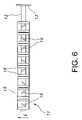
- FIG. 6is a front view of the EBG ESA feed 11 showing an edge-slotted TE 10 waveguide as the linear array feed 12 to the EBG ESA feed 11 . Only portions of the feed 12 are shown.
- the edge-slotted TE 10 waveguide feed 12feeds the EBG ESA feed 11 through slots 16 . It may be possible to use other types of TE 01 coupling that are commonly known in the art such as C slots, I slots, and others.
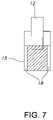
- FIG. 7is a top view of a single EBG waveguide element 15 showing the EBG sidewalls 18 and the feed 12 .
- the feed 12can either be fed from the center or fed from the end with an input flange 13 .
- the EBG ESA feed 11 shownis configured in a linear, vertical polarization (VP) implementation, but a linear horizontal polarization (HP) implementation is also possible by placing the EBG sidewalls 18 on the top and bottom waveguide walls, rather than on the sidewalls, as shown in the figures.
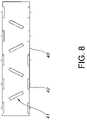
- Another linear polarization feed embodiment to feed the EBG ESA feed 11is to use an EBG linear array described in co-pending patent application Ser. No. 10/458,481 as the feed 12 .
- This feed architectureis a slotted linear one-dimensional EBG waveguide 40 where the narrow walls of the waveguide are lined with either discrete or continuous EBG materials 42 , as illustrated in FIG. 8 . All one-dimensional horn embodiments, as described herein, are applicable to this architecture.
- Circular polarizationeither right hand (RHCP) or left hand (LHCP) is also possible by using a polarizing grid, such as a meander line polarizer that is commonly known in the art, in front of the ESA horn antenna 10 aperture of FIGS. 1 and 2 .
- a polarizing gridsuch as a meander line polarizer that is commonly known in the art
- Circular polarizationis possible when dimension x equals dimension y and ⁇ x ⁇ y ⁇ 90° at the x/y aperture plane.
- This implementationrequires ⁇ y to be further offset from ⁇ x to account for the differences in vertical and horizontal horn flares due to the length of the feed 30 not being equal to the width.
- This additional phase offsetis possible with a fixed phase shift in the non-scanning plane.
- One embodimentwould be to put passive EBG material on the waveguide walls in the non-scan plane.
- the dual-mode EBG waveguide phase shifter linear ESA feed 30 in FIG. 9is made up of dual-mode phase shifters 50 .
- a dual-mode phase shifter 50conceptually illustrated in FIG. 10 , is described in detail in co-pending patent application Ser. Nos. 10/698,774 and 10/699,514.
- a dual-mode analog phase shifter 50may be constructed as shown in FIG. 10 . This allows a second TEM mode to be supported, orthogonal to the first as shown in FIG. 10 . This second TEM mode can operate on or near the same frequency in a frequency band or a different frequency band than the first mode.
- the insertion phase of the second modeis governed by the top and bottom EBG devices 46 on waveguide horizontal surfaces 45 , while the original TEM mode is independently controlled by the EBG devices 18 on the vertical sidewall surfaces 19 .
- Each beamcan be independently steered in this configuration.
- the four-sided pyramidal hornis used to generate independently steered ESA beams, with orthogonal linear polarization and operating in different frequency bands. Orthogonal circular polarization is possible by means of an external polarizer grid, as described in co-pending application Ser. No. 10/699,514.
- linear array feed structures 12 to excite the EBG waveguide phase shifters 15are possible, including rectangular waveguide feeds with slots in the broad wall, single ridge waveguide with slots in either the broad or narrow walls, double-ridged waveguide with end wall coupling slots, and printed feeds such as microstrip, stripline, suspended stripline, coplanar waveguide, fine line, and others commonly know in the art.
- the one-dimensional EBG waveguide phase shifter based ESA horn antenna 10 of the present inventionutilizes the horn 17 to realize increased directivity and a narrower beam with in the non-scanning plane, as previously shown in FIGS. 1 and 2 .
- the horn 17 sidewalls 14can be metallic, which forces a TE 01 at the aperture resulting in ⁇ 18 dB sidelobes in the scan plane.
- the sidewalls 14can be removed, or open, which allows a uniform aperture distribution due to the EBG linear array resulting in a ⁇ 12.5 dB sidelobe level with an optimal minimum beamwidth for a given aperture size.
- the radiation pattern performance of horns with these types of boundary conditionsis commonly known within the art.
- a passive EBG surface or a tunable EBG surfacecan be used to provide some level of beamwidth and sidelobe level adjustment capability.
- the one-dimensional EBG waveguide phase shifter based ESA horn antenna 10can be orientated to scan either in azimuth or elevation, as dictated by the orientation of the feed manifold 11 .
- VP, HP, RCHP, or LHCPcan be realized for either scan plane, as described in the previous discussion on the feed 11 .
- the horn 17 dimensionsdetermine the radiation pattern characteristics of the non-scanned plane. It is also possible to mechanically steer this ESA horn antenna 10 in the non-electronically scanned plane.
Landscapes
- Waveguide Aerials (AREA)
- Variable-Direction Aerials And Aerial Arrays (AREA)
Abstract
Description
The present application is related to co-pending application Ser. No. 10/458,481 filed on Jun. 10, 2003 entitled “One-Dimensional and Two-Dimensional Electronically Scanned Slotted Waveguide Antennas Using Tunable Band Gap Surfaces”; Ser. No. 10/354,280 filed on Jan. 30, 2003 entitled “Frequency Agile Material-Based Reflectarray Antenna” invented by James B. West; Ser. No. 10/273,459 filed on Oct. 18, 2002 entitled “A Method and Structure for Phased Array Antenna Interconnect” invented by John C. Mather, Christina M. Conway, and James B. West; Ser. No. 10/273,872 entitled “A Construction Approach for an EMXT-Based Phased Array Antenna” invented by John C. Mather, Christina M. Conway, James B. West, Gary E. Lehtola, and Joel M. Wichgers; Ser. No. 10/698,774 filed on Oct. 23, 2003 entitled “Independently Controlled Dual-Mode Analog Waveguide Phase Shifter” invented by James B. West and Jonathan P. Doane; and Ser. No. 10/699,514 filed on Oct. 31, 2003 entitled “A Dual-Band Multibeam Waveguide Phased Array” invented by James B. West and Jonathan P. Doane. The co-pending applications are incorporated by reference herein in their entirety. All applications are assigned to the assignee of the present application.
This invention relates to antennas, phased array antennas, and specifically to a one-dimensional electromagnetic band gap (EBG) waveguide phase shifter based electronically scanned array (ESA) horn antenna.
Phased array antennas offer significant system level performance enhancements for advanced communications, data link, radar, and SATCOM systems. The ability to rapidly scan the radiation pattern of the array allows the realization of multi-mode operation, LPI/LPD (low probability of intercept and detection), and A/J (antijam) capablities. One of the major challenges in phased array design is to provide a cost effective and environmentally robust interconnect and construction scheme for the phased array assembly. Additional requirements include phased array antenna phase shifting methods and techniques.
It is well known within the art that the operation of a phased array is approximated to the first order as the product of the array factor and the radiation element pattern as shown inEquation 1 for a linear array.
Standard spherical coordinates are used inEquation 1 and θ is the scan angle referenced to bore sight of the array. Introducing phase shift at all radiating elements within the array changes the argument of the array factor exponential term inEquation 1, which in turns steers the main beam from its nominal position. Phase shifters are RF devices or circuits that provide the required variation in electrical phase. Array element spacing is related to the operating wavelength and sets the scan performance of the array. All radiating element patterns are assumed to be identical for the ideal case where mutual coupling between elements does not exist. The array factor describes the performance of an array of isotropic radiators arranged in a prescribed grid for a two-dimensional rectangular array grid.
Co-pending application Ser. No. 10/273,459 effectively resolves the phased array interconnect problem by utilizing fine pitch, high-density circuitry in a thin self-shielding multi-layer printed wiring assembly. The new approach utilizes the thickness dimension of an array aperture wall (parallel to bore sight axis) to provide the surface area and volume required to implement all of the conductive traces for phase shifter bias, ground, and control lines.
A packaging, interconnect, and construction approach is disclosed in co-pending application Ser. No. 10/273,872 that creates a cost-effective EMXT (electromagnetic crystal)-based phased array antennas having multiple active radiating elements in an X-by-Y configuration. EMXT devices are also known in the art as tunable photonic band gap (PBG) and tunable electromagnetic band gap (EBG) substrates.
A detailed description of a waveguide section with tunable EBG phase shifter technologies is available in a paper by J. A. Higgins et al. “Characteristics of Ka Band Waveguide using Electromagnetic Crystal Sidewalls” 2002 IEEE MTT-S International Microwave Symposium, Seattle, Wash., June 2002. Each element is comprised of EMXT sidewalls and a conductive (metallic) floor and ceiling. Each EMXT device requires a bias voltage plus a ground connection in order to control the phase shift for each element of the antenna by modulating the sidewall impedance of the waveguide. By controlling phase shift performance of the elements, the beam of the antenna can be formed and steered.
One-dimensional electronic beam steering is adequate for many communication and radar systems, with mechanical steering providing adequate beam steering rates on the second dimension, if required. Specific bands of current interest include C- and X-band for SATCOM and meteorological, multimode, and fire control radars, Ku-band (10-12 GHz), Ka-band (20/30 GHz), and Q-band (44 GHz) for satellite communication (SATCOM) systems and 38 GHz for FCS Future Combat Systems (FCS) communications and radar. For example, the FCS ground-to-ground radar/communication function requires only rapid beam scanning in azimuth with a static fan beam in elevation. Another example is an elevation only ESA for commercial multimode weather radar. Additional examples include ground-based SATCOM on-the-move and non-fighter airborne SATCOM that do not require rapid beam agility in two dimensions.
Frequently the above-mentioned systems have extremely aggressive recurring cost requirements. One-dimensional beam scanning significantly reduces the ESA phase shifter count and beam steering computer/interconnect complexity, all which directly contribute to cost. To illustrate this complexity issue, consider the following: to a first order, a N×N, two-dimensional ESA requires N2phase shifters, each with commensurate beam steering control and interconnect requirements, where as a one-dimensional ESA of the same electrical size only requires N phase shifters, control and interconnect. For N=200, the two-dimensional ESA would require 40,000 phase shifters where as the one-dimensional ESA of the same size would require 200 phase shifters.
A need exists for a cost-effective, low-loss, robust, one-dimensional electronically scanned phased arrays with extremely fast beam steering rates.
A one-dimensional electromagnetic band gap (EBG) waveguide phase shifter electronically scanned array (ESA) horn antenna is disclosed. The horn antenna has a linear array of EBG waveguide phase shifters for scanning and radiating a beam. A linear array feed feeds the linear array of EBG waveguide phase shifters. A horn shapes radiation from the linear array of EBG waveguide phase shifters. Each of the EBG waveguide phase shifters comprises a waveguide having vertical and horizontal sidewalls. Electromagnetic band gap devices are located on the vertical waveguide walls and shift phase to scan the beam. The EBG devices comprise a dielectric substrate, a plurality of conductive strips located periodically on a surface of the dielectric substrate and a ground plane located on a surface of the dielectric substrate opposite the plurality of conductive strips. The EBG devices further comprise a plurality of reactive devices placed between the conductive strips to vary reactance between the conductive strips thereby varying a surface impedance of the EBG devices to shift the phase. The reactive devices may be varactor diodes or Schotkky diodes.
The dielectric substrate may be a ferroelectric substrate having a dielectric constant varied with a bias applied to the plurality of conductive strips to shift the phase. The dielectric substrate may be a ferromagnetic substrate having a permeability varied with a bias applied to the plurality of conductive strips to shift the phase.
In the one-dimensional electromagnetic band gap waveguide phase shifter electronically scanned array horn antenna, the linear array feed may be an edge slotted TE10waveguide or a slotted linear one-dimensional EBG waveguide. The horn may be a horn with open sidewalls or a pyramidal horn.
It is an object of the present invention to provide a cost-effective, low-loss, robust, one-dimensional electronically scanned phased array with fast beam steering rates.
It is an object of the present invention to minimize phase shifter count with a one-dimensional scan antenna.
It is an advantage of the present invention to utilize electromagnetic band gap phase shifters to provide high-performance analog phase shifting.
It is an advantage of the present invention to utilize a horn to set gain and beamwidth in an off-scan plane.
It is a feature of the present invention to provide a dual-mode phase shifter capability in a one-dimensional ESA horn antenna.
The invention may be more fully understood by reading the following description of the preferred embodiments of the invention in conjunction with the appended drawings wherein:
The present invention is for a low-cost one-dimensional electromagnetic band gap (EBG) waveguide phase shifter based electronically scanned array (ESA) horn antenna.
The one-dimensional EBG waveguide phase shifter basedESA horn antenna 10 of the present invention can be realized with an EBG waveguide phase shifter-based linear array of several embodiments. The use of EBG waveguide phase shifters offers low-cost solutions for high performance, low loss, and high switching speeds. Another advantage of the present invention is analog phase shifting, which eliminates the quantization side lobes inherent to digital phase shifters and true time delay (TTD) devices in a plane in which an array beam is electronically scanned.
An analog waveguide phaseshifter radiating element 15 using electromagnetic band gap (EBG)devices 18 onwaveguide sidewalls 19 is shown inFIG. 3 . A detailed description of a waveguide section with tunable EBG phase shifter technologies is available in the referenced paper by J. A. Higgins et al. “Characteristics of Ka Band Waveguide using Electromagnetic Crystal Sidewalls”. The paper describes electromagnetic crystal (EMXT) devices implemented with EBG materials. EBG devices have periodic surfaces that become a high impedance (open circuit) to incident waves at their resonant frequency. The surface impedance of a given tunable EBG physical device is a function of the tuning mechanism on the EBG and frequency. The EBG substrate material may be GaAs, ferroelectric, ferromagnetic, or any suitable EBG embodiment.
The waveguide sidewalls19 of the EBGwaveguide phase shifter 15 each contain anEBG device 18 that consists of a periodic surface ofconductive strips 20 that may be metal separated bygaps 21 over a surface of adielectric substrate 25 as shown inFIG. 4 aandFIG. 4 b. Thesestrips 20 capacitively couple to each other and inductively couple to aground plane 30 on an opposite surface of thesubstrate 25 as shown inFIG. 4 b. This structure creates a LC tank circuit shown inFIG. 4 cthat resonates at a desired frequency. Near the desired resonant frequency, theEBG device 18 surface behaves like a high impedance to a wave traveling down the waveguide as shown inFIGS. 4 aand4b, thus allowing a tangential electric field. Since the high impedance also limits current flow, the tangential magnetic field is forced to zero. The fundamental mode of such a structure is therefore TEM (transverse electromagnetic) having a uniform vertical electric field shown byarrow 26 and a uniform horizontal magnetic field (not shown), both transverse to the direction of propagation shown byarrow 27 inFIG. 4 b.
Various methods of tuning theEBG device 18 exist. The most developed is a plurality ofreactive devices 35 such as varactor diodes or Schotkky diodes placed periodically between thestrips 20 to vary a reactance. By adjusting a reverse bias voltage on thediodes 35 applied via the conductivemetallic strips 20 from a control source (not shown), the capacitive coupling between thestrips 20 is varied as shown by a variable capacitor Cv inFIG. 4 c, and the overall surface impedance of theEBG device 18 shifts. With a shift in the surface impedance of theEBG devices 18 on thewaveguide sidewalls 19, the propagation velocity of the wave is also modulated. The insertion phase of the element can therefore be actively controlled, resulting in a 360° analog phase shifter, for a sufficiently long element.
Thetunable EBG device 18 may be implemented in semiconductor MMIC (monolithic microwave integrated circuit) technology. Gallium arsenide (GaAs) and indium phosphide (InP)semiconductor substrates 25 are currently practical, but other III-V and semiconductor compounds are feasible. In these implementations thesemiconductor substrate 25 acts as a passive (non-tunable) dielectric material, and tunability is obtained with thereactive devices 35 such as the varactor or Schotkky diodes inFIG. 4 bconnected across the conductive strips20. The semiconductor device tuning elements, the top side metal geometries and the back side bias control signal line interconnections are all realized by means of commonly know semiconductor fabrication techniques.
Other types of discrete tuning elements are also possible. One example is ferroelectric tunable chip capacitors that can be attached to passive microwave/millimeter wave printed wiring board substrates.
Ferroelectric and ferromagnetic tunable EBG substrates may be used in theEBG device 18 as thedielectric substrate 25 ofFIGS. 4 aand4b. Here the dielectric constant and the permeability are varied with a bias applied to theconductive strips 20 to tune theEBG device 18. Metal deposition techniques are used to form the required top-side metallic geometries and back side bias control signal line interconnections.
Ferroelectric and ferromagnetic materials are known to exhibit electrical parameters of relative permittivity and/or permeability that can be altered or tuned by means of an external stimulus such as a DC bias field. It should be noted, however, that the concepts described herein are equally applicable to any materials that exhibit similar electrical material parameter modulation by means of an external stimulus signal.
Substrates with adjustable material parameters, such as ferroelectric or ferromagnetic materials can be fabricated monolithically, i.e. in a continuous planar substrate without segmentation or subassemblies, through thin film deposition, ceramic fabrication techniques, or semiconductor wafer bulk crystal growth techniques. An example of bulk crystal growth is the Czochralski crystal pulling technique that is known within the art to grow germanium, silicon and a wide range of compound semiconductors, oxides, metals, and halides.
An advantage of using a TEM mode waveguide is that there is no cutoff frequency. In standard TE10mode waveguide (all metal walls), the sidewall-to-sidewall dimension must be greater than λg/2 (one half of a waveguide wavelength). With a TEM mode waveguide, the dimensions are theoretically waveguide cross section independent, and the waveguide can be whatever size is convenient for the application. An application where this is a large advantage is in an open-ended waveguide phased array, where elements must be placed at λ/2 spacing to avoid grating lobes. Air-filled TEM elements can therefore be used where air-filled TE10waveguide elements can not.
An embodiment of the EBG ESA waveguide phase shifting linear array horn feed11 ofFIG. 1 is further illustrated inFIG. 6 .FIG. 6 is a front view of the EBG ESA feed11 showing an edge-slotted TE10waveguide as the linear array feed12 to theEBG ESA feed 11. Only portions of thefeed 12 are shown. The edge-slotted TE10waveguide feed12 feeds the EBG ESA feed11 throughslots 16. It may be possible to use other types of TE01coupling that are commonly known in the art such as C slots, I slots, and others.FIG. 7 is a top view of a singleEBG waveguide element 15 showing the EBG sidewalls18 and thefeed 12. Thefeed 12 can either be fed from the center or fed from the end with aninput flange 13. The EBG ESA feed11 shown is configured in a linear, vertical polarization (VP) implementation, but a linear horizontal polarization (HP) implementation is also possible by placing the EBG sidewalls18 on the top and bottom waveguide walls, rather than on the sidewalls, as shown in the figures.
Another linear polarization feed embodiment to feed the EBG ESA feed11 is to use an EBG linear array described in co-pending patent application Ser. No. 10/458,481 as thefeed 12. This feed architecture is a slotted linear one-dimensional EBG waveguide 40 where the narrow walls of the waveguide are lined with either discrete orcontinuous EBG materials 42, as illustrated inFIG. 8 . All one-dimensional horn embodiments, as described herein, are applicable to this architecture.
Circular polarization (CP), either right hand (RHCP) or left hand (LHCP) is also possible by using a polarizing grid, such as a meander line polarizer that is commonly known in the art, in front of theESA horn antenna 10 aperture ofFIGS. 1 and 2 .
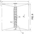
Another embodiment for achieving circular polarization is to feed a square pyramidal horn shown27 inFIG. 9 with a dual-mode EBG waveguide phase shifterlinear ESA feed 30. Circular polarization is possible when dimension x equals dimension y and øx−øy±90° at the x/y aperture plane. This implementation requires øyto be further offset from øxto account for the differences in vertical and horizontal horn flares due to the length of thefeed 30 not being equal to the width. This additional phase offset is possible with a fixed phase shift in the non-scanning plane. One embodiment would be to put passive EBG material on the waveguide walls in the non-scan plane.
The dual-mode EBG waveguide phase shifterlinear ESA feed 30 inFIG. 9 is made up of dual-mode phase shifters 50. A dual-mode phase shifter 50, conceptually illustrated inFIG. 10 , is described in detail in co-pending patent application Ser. Nos. 10/698,774 and 10/699,514. By integratingEBG devices 46 into the top and bottomhorizontal surfaces 45 of the waveguide as well as thesidewalls 19, a dual-modeanalog phase shifter 50 may be constructed as shown inFIG. 10 . This allows a second TEM mode to be supported, orthogonal to the first as shown inFIG. 10 . This second TEM mode can operate on or near the same frequency in a frequency band or a different frequency band than the first mode. The insertion phase of the second mode is governed by the top andbottom EBG devices 46 on waveguidehorizontal surfaces 45, while the original TEM mode is independently controlled by theEBG devices 18 on the vertical sidewall surfaces19. Each beam can be independently steered in this configuration. In this embodiment, the four-sided pyramidal horn is used to generate independently steered ESA beams, with orthogonal linear polarization and operating in different frequency bands. Orthogonal circular polarization is possible by means of an external polarizer grid, as described in co-pending application Ser. No. 10/699,514.
Numerous other lineararray feed structures 12 to excite the EBGwaveguide phase shifters 15 are possible, including rectangular waveguide feeds with slots in the broad wall, single ridge waveguide with slots in either the broad or narrow walls, double-ridged waveguide with end wall coupling slots, and printed feeds such as microstrip, stripline, suspended stripline, coplanar waveguide, fine line, and others commonly know in the art.
The one-dimensional EBG waveguide phase shifter basedESA horn antenna 10 of the present invention utilizes thehorn 17 to realize increased directivity and a narrower beam with in the non-scanning plane, as previously shown inFIGS. 1 and 2 . Thehorn 17sidewalls 14 can be metallic, which forces a TE01at the aperture resulting in −18 dB sidelobes in the scan plane. Alternatively, thesidewalls 14 can be removed, or open, which allows a uniform aperture distribution due to the EBG linear array resulting in a −12.5 dB sidelobe level with an optimal minimum beamwidth for a given aperture size. The radiation pattern performance of horns with these types of boundary conditions is commonly known within the art. In addition, a passive EBG surface or a tunable EBG surface can be used to provide some level of beamwidth and sidelobe level adjustment capability.
The one-dimensional EBG waveguide phase shifter basedESA horn antenna 10 can be orientated to scan either in azimuth or elevation, as dictated by the orientation of thefeed manifold 11. VP, HP, RCHP, or LHCP can be realized for either scan plane, as described in the previous discussion on thefeed 11.
Thehorn 17 dimensions determine the radiation pattern characteristics of the non-scanned plane. It is also possible to mechanically steer thisESA horn antenna 10 in the non-electronically scanned plane.
It is believed that the one-dimensional EBG waveguide phase shifter based ESA horn antenna of the present invention and many of its attendant advantages will be understood by the foregoing description, and it will be apparent that various changes may be made in the form, construction and arrangement of the components thereof without departing from the scope and spirit of the invention or without sacrificing all of its material advantages, the form herein before described being merely an explanatory embodiment thereof. It is the intention of the following claims to encompass and include such changes.
Claims (20)
1. A one-dimensional electromagnetic band gap (EBG) waveguide phase shifter electronically scanned array (ESA) horn antenna comprising:
a linear array of EBG waveguide phase shifters for scanning and radiating a beam;
a linear array feed to feed the linear array of ERG waveguide phase shifters; and
a horn for shaping radiation from the linear array of EBG waveguide phase shifters.
2. The one-dimensional electromagnetic band gap (EBG) waveguide phase shifter electronically scanned array (ESA) horn antenna ofclaim 1 wherein each of the EBG waveguide phase shifters comprises:
a waveguide having vertical and horizontal sidewalls; and
EBG devices on the vertical waveguide walls or the horizontal sidewalls wherein the EBG devices on the vertical walls shift phase to scan the beam with a vertical polarization and wherein the EBG devices on the horizontal walls shift phase to scan the beam with a horizontal polarization.
3. The one-dimensional electromagnetic band gap (EBG) waveguide phase shifter electronically scanned array (ESA) horn antenna ofclaim 2 wherein each of the EBG devices comprise:
a dielectric substrate;
a plurality of conductive strips located periodically on a surface of the dielectric substrate; and
a ground plane located on a surface of the dielectric substrate opposite the plurality of conductive strips.
4. The one-dimensional electromagnetic band gap (EBG) waveguide phase shifter electronically scanned array (ESA) horn antenna ofclaim 3 wherein each of the EBG devices further comprise a plurality of reactive devices placed between the conductive strips to vary reactance between the conductive strips thereby varying a surface impedance of the EBG devices to shift a phase.
5. The one-dimensional electromagnetic band gap (EBG) waveguide phase shifter electronically scanned array (ESA) horn antenna ofclaim 4 wherein the plurality of reactive devices comprises one of varactor diodes, Schotkky diodes, and ferroelectric chip capacitors.
6. The one-dimensional electromagnetic band gap (EBG) waveguide phase shifter electronically scanned array (ESA) horn antenna ofclaim 3 wherein the dielectric substrate is a ferroelectric substrate having a dielectric constant varied with a bias applied to the plurality of conductive strips to shift a phase.
7. The one-dimensional electromagnetic band gap (EBG) waveguide phase shifter electronically scanned array (ESA) horn antenna ofclaim 3 wherein the dielectric substrate is a ferromagnetic substrate having a permeability varied with a bias applied to the plurality of conductive strips to shift a phase.
8. The one-dimensional electromagnetic band gap (EBG) waveguide phase shifter electronically scanned array (ESA) horn antenna ofclaim 1 wherein the linear array feed comprises an edge slotted TE10 waveguide.
9. The one-dimensional electromagnetic band gap (EBG) waveguide phase shifter electronically scanned array (ESA) horn antenna ofclaim 1 wherein the linear array feed comprises a slotted linear one-dimensional EBG waveguide.
10. The one-dimensional electromagnetic band gap (EBG) waveguide phase shifter electronically scanned array (ESA) horn antenna ofclaim 1 wherein the horn comprises one of a horn with open sidewalls and a pyramidal horn.
11. A one-dimensional electromagnetic band gap (EBG) waveguide phase shifter electronically scanned array (ESA) horn antenna for scanning and radiating a beam comprising:
the horn for shaping the scanned and radiated beam
a one-dimensional ESA EBG waveguide phase shifting linear array horn feed for feeding the horn the scanned and radiated beam wherein the one-dimensional ESA EBG waveguide phase shifting linear array horn feed comprises a linear array of EBG waveguide radiating elements; and
a linear array feed for feeding the one-dimensional ESA EBG waveguide phase shifting linear array horn feed.
12. The one-dimensional electromagnetic band gap (EBG) waveguide phase shifter electronically scanned array (ESA) horn antenna ofclaim 11 wherein the EBG waveguide radiating elements each comprise:
a waveguide having vertical and horizontal sidewalls; and
EBG devices on the vertical sidewalls or the horizontal sidewalls wherein the EBG devices on the vertical sidewalls shift phase to scan the beam with a vertical polarization and wherein the EBG devices on the horizontal sidewalls shift phase to scan the beam with a horizontal polarization.
13. The one-dimensional electromagnetic band gap (EBG) waveguide phase shifter electronically scanned array (ESA) horn antenna ofclaim 11 wherein the EBG waveguide radiating elements each comprise:
a waveguide having vertical and horizontal sidewalls; and
EBG devices on the vertical sidewalls and the horizontal sidewalls wherein the EBG devices shift phase to scan the beam.
14. The one-dimensional electromagnetic band gap (EBG) waveguide phase shifter electronically scanned array (ESA) horn antenna ofclaim 13 wherein the EBG devices each comprise:
a dielectric substrate;
a plurality of conductive strips located periodically on a surface of the dielectric substrate; and
a ground plane located on an opposite surface from the conductive strips on the dielectric substrate.
15. The one-dimensional electromagnetic band gap (EBG) waveguide phase shifter electronically scanned array (ESA) horn antenna ofclaim 14 wherein the EBG devices each further comprise a plurality of reactive devices periodically placed between the conductive strips to alter capacitive coupling between the conductive strips thereby varying a surface impedance to shift a phase.
16. The one-dimensional electromagnetic band gap (EBG) waveguide phase shifter electronically scanned array (ESA) horn antenna ofclaim 15 wherein the plurality of reactive devices comprises one of varactor diodes, Schotkky diodes, and ferroelectric chip capacitors.
17. The one-dimensional electromagnetic band gap (EBG) waveguide phase shifter electronically scanned array (ESA) horn antenna ofclaim 13 wherein the EBG devices on the vertical walls phase shift in a first mode and the EBG devices on the horizontal walls phase shift in a second mode independent of the phase shift in the first mode.
18. The one-dimensional electromagnetic band gap (EBG) waveguide phase shifter electronically scanned array (ESA) horn antenna ofclaim 17 wherein the first mode is at a first frequency and the second mode is at a second frequency.
19. The one-dimensional electromagnetic band gap (EBG) waveguide phase shifter electronically scanned array (ESA) horn antenna ofclaim 17 wherein the first mode and the second mode are at a same frequency.
20. A one-dimensional electromagnetic band gap (EBG) waveguide phase shifter electronically scanned array (ESA) horn antenna comprising a linear array of EBG waveguide phase shifters for scanning and radiating a beam; a linear array feed to feed the linear array of EBG waveguide phase shifters; and a horn for directing radiation from the linear array of EBG waveguide phase shifters wherein each of the EBG waveguide phase shifters comprises:
a waveguide having vertical and horizontal sidewalls; and
EBG devices on the vertical sidewalls wherein the EBG devices on the vertical sidewalls phase shift to scan the beam said EBG devices each comprise:
a dielectric substrate;
a plurality of conductive strips periodically located on a surface of the dielectric substrate;
a ground plane located on a surface of the dielectric substrate opposite the plurality of conductive strips; and
a plurality of reactive devices placed between the conductive strips to vary reactance between the conductive strips thereby varying a surface impedance of the EBG devices to shift a phase.
Priority Applications (1)
| Application Number | Priority Date | Filing Date | Title |
|---|---|---|---|
| US10/891,910US7307596B1 (en) | 2004-07-15 | 2004-07-15 | Low-cost one-dimensional electromagnetic band gap waveguide phase shifter based ESA horn antenna |
Applications Claiming Priority (1)
| Application Number | Priority Date | Filing Date | Title |
|---|---|---|---|
| US10/891,910US7307596B1 (en) | 2004-07-15 | 2004-07-15 | Low-cost one-dimensional electromagnetic band gap waveguide phase shifter based ESA horn antenna |
Publications (1)
| Publication Number | Publication Date |
|---|---|
| US7307596B1true US7307596B1 (en) | 2007-12-11 |
Family
ID=38792871
Family Applications (1)
| Application Number | Title | Priority Date | Filing Date |
|---|---|---|---|
| US10/891,910Expired - LifetimeUS7307596B1 (en) | 2004-07-15 | 2004-07-15 | Low-cost one-dimensional electromagnetic band gap waveguide phase shifter based ESA horn antenna |
Country Status (1)
| Country | Link |
|---|---|
| US (1) | US7307596B1 (en) |
Cited By (194)
| Publication number | Priority date | Publication date | Assignee | Title |
|---|---|---|---|---|
| US20080291115A1 (en)* | 2007-05-22 | 2008-11-27 | Sibeam, Inc. | Surface mountable integrated circuit packaging scheme |
| US7917255B1 (en) | 2007-09-18 | 2011-03-29 | Rockwell Colllins, Inc. | System and method for on-board adaptive characterization of aircraft turbulence susceptibility as a function of radar observables |
| US20110140541A1 (en)* | 2009-12-14 | 2011-06-16 | Samsung Electronics Co., Ltd. | Battery pack with wireless power transmission resonator |
| WO2012050614A1 (en)* | 2010-10-15 | 2012-04-19 | Searete Llc | Surface scattering antennas |
| US20130241791A1 (en)* | 2012-03-16 | 2013-09-19 | Raytheon Company | Ridged Waveguide Flared Radiator Array Using Electromagnetic Bandgap Material |
| DE102012007748A1 (en)* | 2012-04-18 | 2013-10-24 | Eads Deutschland Gmbh | Antenna, has radiator element attached to transmission/receiving module, and waveguide provided with radiator elements as slots and connected with transmission/receiving module over waveguide component implemented as adapter |
| US8604990B1 (en)* | 2009-05-23 | 2013-12-10 | Victory Microwave Corporation | Ridged waveguide slot array |
| US8648768B2 (en) | 2011-01-31 | 2014-02-11 | Ball Aerospace & Technologies Corp. | Conical switched beam antenna method and apparatus |
| US9119127B1 (en) | 2012-12-05 | 2015-08-25 | At&T Intellectual Property I, Lp | Backhaul link for distributed antenna system |
| US9154966B2 (en) | 2013-11-06 | 2015-10-06 | At&T Intellectual Property I, Lp | Surface-wave communications and methods thereof |
| US9209902B2 (en) | 2013-12-10 | 2015-12-08 | At&T Intellectual Property I, L.P. | Quasi-optical coupler |
| US9312919B1 (en) | 2014-10-21 | 2016-04-12 | At&T Intellectual Property I, Lp | Transmission device with impairment compensation and methods for use therewith |
| US9323877B2 (en) | 2013-11-12 | 2016-04-26 | Raytheon Company | Beam-steered wide bandwidth electromagnetic band gap antenna |
| US9368878B2 (en) | 2009-05-23 | 2016-06-14 | Pyras Technology Inc. | Ridge waveguide slot array for broadband application |
| US9379437B1 (en) | 2011-01-31 | 2016-06-28 | Ball Aerospace & Technologies Corp. | Continuous horn circular array antenna system |
| US9385435B2 (en) | 2013-03-15 | 2016-07-05 | The Invention Science Fund I, Llc | Surface scattering antenna improvements |
| US9448305B2 (en) | 2014-03-26 | 2016-09-20 | Elwha Llc | Surface scattering antenna array |
| US9461706B1 (en) | 2015-07-31 | 2016-10-04 | At&T Intellectual Property I, Lp | Method and apparatus for exchanging communication signals |
| US9490869B1 (en) | 2015-05-14 | 2016-11-08 | At&T Intellectual Property I, L.P. | Transmission medium having multiple cores and methods for use therewith |
| US9503189B2 (en) | 2014-10-10 | 2016-11-22 | At&T Intellectual Property I, L.P. | Method and apparatus for arranging communication sessions in a communication system |
| US9509415B1 (en) | 2015-06-25 | 2016-11-29 | At&T Intellectual Property I, L.P. | Methods and apparatus for inducing a fundamental wave mode on a transmission medium |
| US9520945B2 (en) | 2014-10-21 | 2016-12-13 | At&T Intellectual Property I, L.P. | Apparatus for providing communication services and methods thereof |
| US9525524B2 (en) | 2013-05-31 | 2016-12-20 | At&T Intellectual Property I, L.P. | Remote distributed antenna system |
| US9525210B2 (en) | 2014-10-21 | 2016-12-20 | At&T Intellectual Property I, L.P. | Guided-wave transmission device with non-fundamental mode propagation and methods for use therewith |
| US9531427B2 (en) | 2014-11-20 | 2016-12-27 | At&T Intellectual Property I, L.P. | Transmission device with mode division multiplexing and methods for use therewith |
| US9564947B2 (en) | 2014-10-21 | 2017-02-07 | At&T Intellectual Property I, L.P. | Guided-wave transmission device with diversity and methods for use therewith |
| US9577307B2 (en) | 2014-10-21 | 2017-02-21 | At&T Intellectual Property I, L.P. | Guided-wave transmission device and methods for use therewith |
| US9608740B2 (en) | 2015-07-15 | 2017-03-28 | At&T Intellectual Property I, L.P. | Method and apparatus for launching a wave mode that mitigates interference |
| US9608692B2 (en) | 2015-06-11 | 2017-03-28 | At&T Intellectual Property I, L.P. | Repeater and methods for use therewith |
| US9615269B2 (en) | 2014-10-02 | 2017-04-04 | At&T Intellectual Property I, L.P. | Method and apparatus that provides fault tolerance in a communication network |
| US9628854B2 (en) | 2014-09-29 | 2017-04-18 | At&T Intellectual Property I, L.P. | Method and apparatus for distributing content in a communication network |
| US9628116B2 (en) | 2015-07-14 | 2017-04-18 | At&T Intellectual Property I, L.P. | Apparatus and methods for transmitting wireless signals |
| US9640850B2 (en) | 2015-06-25 | 2017-05-02 | At&T Intellectual Property I, L.P. | Methods and apparatus for inducing a non-fundamental wave mode on a transmission medium |
| US9647345B2 (en) | 2013-10-21 | 2017-05-09 | Elwha Llc | Antenna system facilitating reduction of interfering signals |
| US9653770B2 (en) | 2014-10-21 | 2017-05-16 | At&T Intellectual Property I, L.P. | Guided wave coupler, coupling module and methods for use therewith |
| US9654173B2 (en) | 2014-11-20 | 2017-05-16 | At&T Intellectual Property I, L.P. | Apparatus for powering a communication device and methods thereof |
| US9667317B2 (en) | 2015-06-15 | 2017-05-30 | At&T Intellectual Property I, L.P. | Method and apparatus for providing security using network traffic adjustments |
| US9680670B2 (en) | 2014-11-20 | 2017-06-13 | At&T Intellectual Property I, L.P. | Transmission device with channel equalization and control and methods for use therewith |
| US9685992B2 (en) | 2014-10-03 | 2017-06-20 | At&T Intellectual Property I, L.P. | Circuit panel network and methods thereof |
| US9692101B2 (en) | 2014-08-26 | 2017-06-27 | At&T Intellectual Property I, L.P. | Guided wave couplers for coupling electromagnetic waves between a waveguide surface and a surface of a wire |
| US9705571B2 (en) | 2015-09-16 | 2017-07-11 | At&T Intellectual Property I, L.P. | Method and apparatus for use with a radio distributed antenna system |
| US9705561B2 (en) | 2015-04-24 | 2017-07-11 | At&T Intellectual Property I, L.P. | Directional coupling device and methods for use therewith |
| US9711852B2 (en) | 2014-06-20 | 2017-07-18 | The Invention Science Fund I Llc | Modulation patterns for surface scattering antennas |
| US9722318B2 (en) | 2015-07-14 | 2017-08-01 | At&T Intellectual Property I, L.P. | Method and apparatus for coupling an antenna to a device |
| US9729197B2 (en) | 2015-10-01 | 2017-08-08 | At&T Intellectual Property I, L.P. | Method and apparatus for communicating network management traffic over a network |
| US9735833B2 (en) | 2015-07-31 | 2017-08-15 | At&T Intellectual Property I, L.P. | Method and apparatus for communications management in a neighborhood network |
| US9742462B2 (en) | 2014-12-04 | 2017-08-22 | At&T Intellectual Property I, L.P. | Transmission medium and communication interfaces and methods for use therewith |
| US9748626B2 (en) | 2015-05-14 | 2017-08-29 | At&T Intellectual Property I, L.P. | Plurality of cables having different cross-sectional shapes which are bundled together to form a transmission medium |
| US9749053B2 (en) | 2015-07-23 | 2017-08-29 | At&T Intellectual Property I, L.P. | Node device, repeater and methods for use therewith |
| US9749013B2 (en) | 2015-03-17 | 2017-08-29 | At&T Intellectual Property I, L.P. | Method and apparatus for reducing attenuation of electromagnetic waves guided by a transmission medium |
| US9755697B2 (en) | 2014-09-15 | 2017-09-05 | At&T Intellectual Property I, L.P. | Method and apparatus for sensing a condition in a transmission medium of electromagnetic waves |
| US9762289B2 (en) | 2014-10-14 | 2017-09-12 | At&T Intellectual Property I, L.P. | Method and apparatus for transmitting or receiving signals in a transportation system |
| US9769020B2 (en) | 2014-10-21 | 2017-09-19 | At&T Intellectual Property I, L.P. | Method and apparatus for responding to events affecting communications in a communication network |
| US9769128B2 (en) | 2015-09-28 | 2017-09-19 | At&T Intellectual Property I, L.P. | Method and apparatus for encryption of communications over a network |
| US9780834B2 (en) | 2014-10-21 | 2017-10-03 | At&T Intellectual Property I, L.P. | Method and apparatus for transmitting electromagnetic waves |
| US9793954B2 (en) | 2015-04-28 | 2017-10-17 | At&T Intellectual Property I, L.P. | Magnetic coupling device and methods for use therewith |
| US9793955B2 (en) | 2015-04-24 | 2017-10-17 | At&T Intellectual Property I, Lp | Passive electrical coupling device and methods for use therewith |
| US9793951B2 (en) | 2015-07-15 | 2017-10-17 | At&T Intellectual Property I, L.P. | Method and apparatus for launching a wave mode that mitigates interference |
| US9800327B2 (en) | 2014-11-20 | 2017-10-24 | At&T Intellectual Property I, L.P. | Apparatus for controlling operations of a communication device and methods thereof |
| US9820146B2 (en) | 2015-06-12 | 2017-11-14 | At&T Intellectual Property I, L.P. | Method and apparatus for authentication and identity management of communicating devices |
| US9825358B2 (en) | 2013-12-17 | 2017-11-21 | Elwha Llc | System wirelessly transferring power to a target device over a modeled transmission pathway without exceeding a radiation limit for human beings |
| US9838896B1 (en) | 2016-12-09 | 2017-12-05 | At&T Intellectual Property I, L.P. | Method and apparatus for assessing network coverage |
| US9836957B2 (en) | 2015-07-14 | 2017-12-05 | At&T Intellectual Property I, L.P. | Method and apparatus for communicating with premises equipment |
| US9843103B2 (en) | 2014-03-26 | 2017-12-12 | Elwha Llc | Methods and apparatus for controlling a surface scattering antenna array |
| US9847566B2 (en) | 2015-07-14 | 2017-12-19 | At&T Intellectual Property I, L.P. | Method and apparatus for adjusting a field of a signal to mitigate interference |
| US9847850B2 (en) | 2014-10-14 | 2017-12-19 | At&T Intellectual Property I, L.P. | Method and apparatus for adjusting a mode of communication in a communication network |
| US9853342B2 (en) | 2015-07-14 | 2017-12-26 | At&T Intellectual Property I, L.P. | Dielectric transmission medium connector and methods for use therewith |
| US9853361B2 (en) | 2014-05-02 | 2017-12-26 | The Invention Science Fund I Llc | Surface scattering antennas with lumped elements |
| US9860075B1 (en) | 2016-08-26 | 2018-01-02 | At&T Intellectual Property I, L.P. | Method and communication node for broadband distribution |
| US9865911B2 (en) | 2015-06-25 | 2018-01-09 | At&T Intellectual Property I, L.P. | Waveguide system for slot radiating first electromagnetic waves that are combined into a non-fundamental wave mode second electromagnetic wave on a transmission medium |
| US9866309B2 (en) | 2015-06-03 | 2018-01-09 | At&T Intellectual Property I, Lp | Host node device and methods for use therewith |
| US9871283B2 (en) | 2015-07-23 | 2018-01-16 | At&T Intellectual Property I, Lp | Transmission medium having a dielectric core comprised of plural members connected by a ball and socket configuration |
| US9871282B2 (en) | 2015-05-14 | 2018-01-16 | At&T Intellectual Property I, L.P. | At least one transmission medium having a dielectric surface that is covered at least in part by a second dielectric |
| US9876570B2 (en) | 2015-02-20 | 2018-01-23 | At&T Intellectual Property I, Lp | Guided-wave transmission device with non-fundamental mode propagation and methods for use therewith |
| US9876264B2 (en) | 2015-10-02 | 2018-01-23 | At&T Intellectual Property I, Lp | Communication system, guided wave switch and methods for use therewith |
| US9876605B1 (en) | 2016-10-21 | 2018-01-23 | At&T Intellectual Property I, L.P. | Launcher and coupling system to support desired guided wave mode |
| US9882257B2 (en) | 2015-07-14 | 2018-01-30 | At&T Intellectual Property I, L.P. | Method and apparatus for launching a wave mode that mitigates interference |
| US9882277B2 (en) | 2015-10-02 | 2018-01-30 | At&T Intellectual Property I, Lp | Communication device and antenna assembly with actuated gimbal mount |
| US9882288B2 (en) | 2014-05-02 | 2018-01-30 | The Invention Science Fund I Llc | Slotted surface scattering antennas |
| US9887456B2 (en) | 2014-02-19 | 2018-02-06 | Kymeta Corporation | Dynamic polarization and coupling control from a steerable cylindrically fed holographic antenna |
| US9893795B1 (en) | 2016-12-07 | 2018-02-13 | At&T Intellectual Property I, Lp | Method and repeater for broadband distribution |
| US9904535B2 (en) | 2015-09-14 | 2018-02-27 | At&T Intellectual Property I, L.P. | Method and apparatus for distributing software |
| US9906269B2 (en) | 2014-09-17 | 2018-02-27 | At&T Intellectual Property I, L.P. | Monitoring and mitigating conditions in a communication network |
| US9912419B1 (en) | 2016-08-24 | 2018-03-06 | At&T Intellectual Property I, L.P. | Method and apparatus for managing a fault in a distributed antenna system |
| US9912027B2 (en) | 2015-07-23 | 2018-03-06 | At&T Intellectual Property I, L.P. | Method and apparatus for exchanging communication signals |
| US9911020B1 (en) | 2016-12-08 | 2018-03-06 | At&T Intellectual Property I, L.P. | Method and apparatus for tracking via a radio frequency identification device |
| US9912382B2 (en) | 2015-06-03 | 2018-03-06 | At&T Intellectual Property I, Lp | Network termination and methods for use therewith |
| US9913139B2 (en) | 2015-06-09 | 2018-03-06 | At&T Intellectual Property I, L.P. | Signal fingerprinting for authentication of communicating devices |
| US9917341B2 (en) | 2015-05-27 | 2018-03-13 | At&T Intellectual Property I, L.P. | Apparatus and method for launching electromagnetic waves and for modifying radial dimensions of the propagating electromagnetic waves |
| US9923271B2 (en) | 2013-10-21 | 2018-03-20 | Elwha Llc | Antenna system having at least two apertures facilitating reduction of interfering signals |
| US9927517B1 (en) | 2016-12-06 | 2018-03-27 | At&T Intellectual Property I, L.P. | Apparatus and methods for sensing rainfall |
| US9935375B2 (en) | 2013-12-10 | 2018-04-03 | Elwha Llc | Surface scattering reflector antenna |
| US9948333B2 (en) | 2015-07-23 | 2018-04-17 | At&T Intellectual Property I, L.P. | Method and apparatus for wireless communications to mitigate interference |
| US9948354B2 (en) | 2015-04-28 | 2018-04-17 | At&T Intellectual Property I, L.P. | Magnetic coupling device with reflective plate and methods for use therewith |
| US9954287B2 (en) | 2014-11-20 | 2018-04-24 | At&T Intellectual Property I, L.P. | Apparatus for converting wireless signals and electromagnetic waves and methods thereof |
| US9967173B2 (en) | 2015-07-31 | 2018-05-08 | At&T Intellectual Property I, L.P. | Method and apparatus for authentication and identity management of communicating devices |
| US9973940B1 (en) | 2017-02-27 | 2018-05-15 | At&T Intellectual Property I, L.P. | Apparatus and methods for dynamic impedance matching of a guided wave launcher |
| US9991580B2 (en) | 2016-10-21 | 2018-06-05 | At&T Intellectual Property I, L.P. | Launcher and coupling system for guided wave mode cancellation |
| US9997819B2 (en) | 2015-06-09 | 2018-06-12 | At&T Intellectual Property I, L.P. | Transmission medium and method for facilitating propagation of electromagnetic waves via a core |
| US9999038B2 (en) | 2013-05-31 | 2018-06-12 | At&T Intellectual Property I, L.P. | Remote distributed antenna system |
| US9998870B1 (en) | 2016-12-08 | 2018-06-12 | At&T Intellectual Property I, L.P. | Method and apparatus for proximity sensing |
| US10009067B2 (en) | 2014-12-04 | 2018-06-26 | At&T Intellectual Property I, L.P. | Method and apparatus for configuring a communication interface |
| US10009901B2 (en) | 2015-09-16 | 2018-06-26 | At&T Intellectual Property I, L.P. | Method, apparatus, and computer-readable storage medium for managing utilization of wireless resources between base stations |
| US10009063B2 (en) | 2015-09-16 | 2018-06-26 | At&T Intellectual Property I, L.P. | Method and apparatus for use with a radio distributed antenna system having an out-of-band reference signal |
| US10009065B2 (en) | 2012-12-05 | 2018-06-26 | At&T Intellectual Property I, L.P. | Backhaul link for distributed antenna system |
| US10020844B2 (en) | 2016-12-06 | 2018-07-10 | T&T Intellectual Property I, L.P. | Method and apparatus for broadcast communication via guided waves |
| US10020587B2 (en) | 2015-07-31 | 2018-07-10 | At&T Intellectual Property I, L.P. | Radial antenna and methods for use therewith |
| US10027397B2 (en) | 2016-12-07 | 2018-07-17 | At&T Intellectual Property I, L.P. | Distributed antenna system and methods for use therewith |
| US10033108B2 (en) | 2015-07-14 | 2018-07-24 | At&T Intellectual Property I, L.P. | Apparatus and methods for generating an electromagnetic wave having a wave mode that mitigates interference |
| US10033107B2 (en) | 2015-07-14 | 2018-07-24 | At&T Intellectual Property I, L.P. | Method and apparatus for coupling an antenna to a device |
| US10044409B2 (en) | 2015-07-14 | 2018-08-07 | At&T Intellectual Property I, L.P. | Transmission medium and methods for use therewith |
| US10051483B2 (en) | 2015-10-16 | 2018-08-14 | At&T Intellectual Property I, L.P. | Method and apparatus for directing wireless signals |
| US10051629B2 (en) | 2015-09-16 | 2018-08-14 | At&T Intellectual Property I, L.P. | Method and apparatus for use with a radio distributed antenna system having an in-band reference signal |
| US10069535B2 (en) | 2016-12-08 | 2018-09-04 | At&T Intellectual Property I, L.P. | Apparatus and methods for launching electromagnetic waves having a certain electric field structure |
| US10074890B2 (en) | 2015-10-02 | 2018-09-11 | At&T Intellectual Property I, L.P. | Communication device and antenna with integrated light assembly |
| US10079661B2 (en) | 2015-09-16 | 2018-09-18 | At&T Intellectual Property I, L.P. | Method and apparatus for use with a radio distributed antenna system having a clock reference |
| US10090606B2 (en) | 2015-07-15 | 2018-10-02 | At&T Intellectual Property I, L.P. | Antenna system with dielectric array and methods for use therewith |
| US10090594B2 (en) | 2016-11-23 | 2018-10-02 | At&T Intellectual Property I, L.P. | Antenna system having structural configurations for assembly |
| US10103422B2 (en) | 2016-12-08 | 2018-10-16 | At&T Intellectual Property I, L.P. | Method and apparatus for mounting network devices |
| US10103801B2 (en) | 2015-06-03 | 2018-10-16 | At&T Intellectual Property I, L.P. | Host node device and methods for use therewith |
| US10135145B2 (en) | 2016-12-06 | 2018-11-20 | At&T Intellectual Property I, L.P. | Apparatus and methods for generating an electromagnetic wave along a transmission medium |
| US10136434B2 (en) | 2015-09-16 | 2018-11-20 | At&T Intellectual Property I, L.P. | Method and apparatus for use with a radio distributed antenna system having an ultra-wideband control channel |
| US10135137B2 (en) | 2015-02-20 | 2018-11-20 | Northrop Grumman Systems Corporation | Low cost space-fed reconfigurable phased array for spacecraft and aircraft applications |
| US10135147B2 (en) | 2016-10-18 | 2018-11-20 | At&T Intellectual Property I, L.P. | Apparatus and methods for launching guided waves via an antenna |
| US10135146B2 (en) | 2016-10-18 | 2018-11-20 | At&T Intellectual Property I, L.P. | Apparatus and methods for launching guided waves via circuits |
| US10139820B2 (en) | 2016-12-07 | 2018-11-27 | At&T Intellectual Property I, L.P. | Method and apparatus for deploying equipment of a communication system |
| US10142086B2 (en) | 2015-06-11 | 2018-11-27 | At&T Intellectual Property I, L.P. | Repeater and methods for use therewith |
| US10144036B2 (en) | 2015-01-30 | 2018-12-04 | At&T Intellectual Property I, L.P. | Method and apparatus for mitigating interference affecting a propagation of electromagnetic waves guided by a transmission medium |
| US10148016B2 (en) | 2015-07-14 | 2018-12-04 | At&T Intellectual Property I, L.P. | Apparatus and methods for communicating utilizing an antenna array |
| US10154493B2 (en) | 2015-06-03 | 2018-12-11 | At&T Intellectual Property I, L.P. | Network termination and methods for use therewith |
| US10168695B2 (en) | 2016-12-07 | 2019-01-01 | At&T Intellectual Property I, L.P. | Method and apparatus for controlling an unmanned aircraft |
| US10170840B2 (en) | 2015-07-14 | 2019-01-01 | At&T Intellectual Property I, L.P. | Apparatus and methods for sending or receiving electromagnetic signals |
| US10178445B2 (en) | 2016-11-23 | 2019-01-08 | At&T Intellectual Property I, L.P. | Methods, devices, and systems for load balancing between a plurality of waveguides |
| US10178560B2 (en) | 2015-06-15 | 2019-01-08 | The Invention Science Fund I Llc | Methods and systems for communication with beamforming antennas |
| US10205655B2 (en) | 2015-07-14 | 2019-02-12 | At&T Intellectual Property I, L.P. | Apparatus and methods for communicating utilizing an antenna array and multiple communication paths |
| US10225025B2 (en) | 2016-11-03 | 2019-03-05 | At&T Intellectual Property I, L.P. | Method and apparatus for detecting a fault in a communication system |
| US10224634B2 (en) | 2016-11-03 | 2019-03-05 | At&T Intellectual Property I, L.P. | Methods and apparatus for adjusting an operational characteristic of an antenna |
| US10243784B2 (en) | 2014-11-20 | 2019-03-26 | At&T Intellectual Property I, L.P. | System for generating topology information and methods thereof |
| US10243270B2 (en) | 2016-12-07 | 2019-03-26 | At&T Intellectual Property I, L.P. | Beam adaptive multi-feed dielectric antenna system and methods for use therewith |
| US10249953B2 (en) | 2015-11-10 | 2019-04-02 | Raytheon Company | Directive fixed beam ramp EBG antenna |
| US10256548B2 (en)* | 2014-01-31 | 2019-04-09 | Kymeta Corporation | Ridged waveguide feed structures for reconfigurable antenna |
| US10264586B2 (en) | 2016-12-09 | 2019-04-16 | At&T Mobility Ii Llc | Cloud-based packet controller and methods for use therewith |
| US10291334B2 (en) | 2016-11-03 | 2019-05-14 | At&T Intellectual Property I, L.P. | System for detecting a fault in a communication system |
| US10291311B2 (en) | 2016-09-09 | 2019-05-14 | At&T Intellectual Property I, L.P. | Method and apparatus for mitigating a fault in a distributed antenna system |
| US10298293B2 (en) | 2017-03-13 | 2019-05-21 | At&T Intellectual Property I, L.P. | Apparatus of communication utilizing wireless network devices |
| US10305190B2 (en) | 2016-12-01 | 2019-05-28 | At&T Intellectual Property I, L.P. | Reflecting dielectric antenna system and methods for use therewith |
| US10312567B2 (en) | 2016-10-26 | 2019-06-04 | At&T Intellectual Property I, L.P. | Launcher with planar strip antenna and methods for use therewith |
| US10320586B2 (en) | 2015-07-14 | 2019-06-11 | At&T Intellectual Property I, L.P. | Apparatus and methods for generating non-interfering electromagnetic waves on an insulated transmission medium |
| US10326689B2 (en) | 2016-12-08 | 2019-06-18 | At&T Intellectual Property I, L.P. | Method and system for providing alternative communication paths |
| US10326494B2 (en) | 2016-12-06 | 2019-06-18 | At&T Intellectual Property I, L.P. | Apparatus for measurement de-embedding and methods for use therewith |
| US10340573B2 (en) | 2016-10-26 | 2019-07-02 | At&T Intellectual Property I, L.P. | Launcher with cylindrical coupling device and methods for use therewith |
| US10340601B2 (en) | 2016-11-23 | 2019-07-02 | At&T Intellectual Property I, L.P. | Multi-antenna system and methods for use therewith |
| US10340983B2 (en) | 2016-12-09 | 2019-07-02 | At&T Intellectual Property I, L.P. | Method and apparatus for surveying remote sites via guided wave communications |
| US10340600B2 (en) | 2016-10-18 | 2019-07-02 | At&T Intellectual Property I, L.P. | Apparatus and methods for launching guided waves via plural waveguide systems |
| US10341142B2 (en) | 2015-07-14 | 2019-07-02 | At&T Intellectual Property I, L.P. | Apparatus and methods for generating non-interfering electromagnetic waves on an uninsulated conductor |
| US10340603B2 (en) | 2016-11-23 | 2019-07-02 | At&T Intellectual Property I, L.P. | Antenna system having shielded structural configurations for assembly |
| US10348391B2 (en) | 2015-06-03 | 2019-07-09 | At&T Intellectual Property I, L.P. | Client node device with frequency conversion and methods for use therewith |
| US10355367B2 (en) | 2015-10-16 | 2019-07-16 | At&T Intellectual Property I, L.P. | Antenna structure for exchanging wireless signals |
| US10361489B2 (en) | 2016-12-01 | 2019-07-23 | At&T Intellectual Property I, L.P. | Dielectric dish antenna system and methods for use therewith |
| US10361481B2 (en) | 2016-10-31 | 2019-07-23 | The Invention Science Fund I, Llc | Surface scattering antennas with frequency shifting for mutual coupling mitigation |
| US10359749B2 (en) | 2016-12-07 | 2019-07-23 | At&T Intellectual Property I, L.P. | Method and apparatus for utilities management via guided wave communication |
| US10374316B2 (en) | 2016-10-21 | 2019-08-06 | At&T Intellectual Property I, L.P. | System and dielectric antenna with non-uniform dielectric |
| US10382976B2 (en) | 2016-12-06 | 2019-08-13 | At&T Intellectual Property I, L.P. | Method and apparatus for managing wireless communications based on communication paths and network device positions |
| US10389037B2 (en) | 2016-12-08 | 2019-08-20 | At&T Intellectual Property I, L.P. | Apparatus and methods for selecting sections of an antenna array and use therewith |
| US10389029B2 (en) | 2016-12-07 | 2019-08-20 | At&T Intellectual Property I, L.P. | Multi-feed dielectric antenna system with core selection and methods for use therewith |
| US10396887B2 (en) | 2015-06-03 | 2019-08-27 | At&T Intellectual Property I, L.P. | Client node device and methods for use therewith |
| US10411356B2 (en) | 2016-12-08 | 2019-09-10 | At&T Intellectual Property I, L.P. | Apparatus and methods for selectively targeting communication devices with an antenna array |
| US10439675B2 (en) | 2016-12-06 | 2019-10-08 | At&T Intellectual Property I, L.P. | Method and apparatus for repeating guided wave communication signals |
| US10446903B2 (en) | 2014-05-02 | 2019-10-15 | The Invention Science Fund I, Llc | Curved surface scattering antennas |
| US10446936B2 (en) | 2016-12-07 | 2019-10-15 | At&T Intellectual Property I, L.P. | Multi-feed dielectric antenna system and methods for use therewith |
| US10498044B2 (en) | 2016-11-03 | 2019-12-03 | At&T Intellectual Property I, L.P. | Apparatus for configuring a surface of an antenna |
| US10530505B2 (en) | 2016-12-08 | 2020-01-07 | At&T Intellectual Property I, L.P. | Apparatus and methods for launching electromagnetic waves along a transmission medium |
| US10535928B2 (en) | 2016-11-23 | 2020-01-14 | At&T Intellectual Property I, L.P. | Antenna system and methods for use therewith |
| US10547348B2 (en) | 2016-12-07 | 2020-01-28 | At&T Intellectual Property I, L.P. | Method and apparatus for switching transmission mediums in a communication system |
| US10553940B1 (en) | 2018-08-30 | 2020-02-04 | Viasat, Inc. | Antenna array with independently rotated radiating elements |
| US10601494B2 (en) | 2016-12-08 | 2020-03-24 | At&T Intellectual Property I, L.P. | Dual-band communication device and method for use therewith |
| US10615506B1 (en) | 2017-07-05 | 2020-04-07 | United States Of America, As Represented By The Secretary Of The Navy | Optically controlled reflect phased array based on photosensitive reactive elements |
| US10637149B2 (en) | 2016-12-06 | 2020-04-28 | At&T Intellectual Property I, L.P. | Injection molded dielectric antenna and methods for use therewith |
| US10650940B2 (en) | 2015-05-15 | 2020-05-12 | At&T Intellectual Property I, L.P. | Transmission medium having a conductive material and methods for use therewith |
| US10665942B2 (en) | 2015-10-16 | 2020-05-26 | At&T Intellectual Property I, L.P. | Method and apparatus for adjusting wireless communications |
| US10679767B2 (en) | 2015-05-15 | 2020-06-09 | At&T Intellectual Property I, L.P. | Transmission medium having a conductive material and methods for use therewith |
| US10694379B2 (en) | 2016-12-06 | 2020-06-23 | At&T Intellectual Property I, L.P. | Waveguide system with device-based authentication and methods for use therewith |
| US10727599B2 (en) | 2016-12-06 | 2020-07-28 | At&T Intellectual Property I, L.P. | Launcher with slot antenna and methods for use therewith |
| US10755542B2 (en) | 2016-12-06 | 2020-08-25 | At&T Intellectual Property I, L.P. | Method and apparatus for surveillance via guided wave communication |
| US10777873B2 (en) | 2016-12-08 | 2020-09-15 | At&T Intellectual Property I, L.P. | Method and apparatus for mounting network devices |
| US10784670B2 (en) | 2015-07-23 | 2020-09-22 | At&T Intellectual Property I, L.P. | Antenna support for aligning an antenna |
| US10811767B2 (en) | 2016-10-21 | 2020-10-20 | At&T Intellectual Property I, L.P. | System and dielectric antenna with convex dielectric radome |
| US10819035B2 (en) | 2016-12-06 | 2020-10-27 | At&T Intellectual Property I, L.P. | Launcher with helical antenna and methods for use therewith |
| US10892553B2 (en) | 2018-01-17 | 2021-01-12 | Kymeta Corporation | Broad tunable bandwidth radial line slot antenna |
| US10916969B2 (en) | 2016-12-08 | 2021-02-09 | At&T Intellectual Property I, L.P. | Method and apparatus for providing power using an inductive coupling |
| US10938108B2 (en) | 2016-12-08 | 2021-03-02 | At&T Intellectual Property I, L.P. | Frequency selective multi-feed dielectric antenna system and methods for use therewith |
| US11032819B2 (en) | 2016-09-15 | 2021-06-08 | At&T Intellectual Property I, L.P. | Method and apparatus for use with a radio distributed antenna system having a control channel reference signal |
| US11165149B2 (en) | 2020-01-30 | 2021-11-02 | Aptiv Technologies Limited | Electromagnetic band gap structure (EBG) |
| US20220365208A1 (en)* | 2021-05-11 | 2022-11-17 | Meteorological Observation Centre of China | Spherical dual-polarization phased array weather radar |
Citations (22)
| Publication number | Priority date | Publication date | Assignee | Title |
|---|---|---|---|---|
| US4198640A (en) | 1978-06-22 | 1980-04-15 | Rca Corporation | Reflectarray antenna |
| US4229745A (en)* | 1979-04-30 | 1980-10-21 | International Telephone And Telegraph Corporation | Edge slotted waveguide antenna array with selectable radiation direction |
| US4323901A (en) | 1980-02-19 | 1982-04-06 | Rockwell International Corporation | Monolithic, voltage controlled, phased array |
| US5170140A (en) | 1988-08-11 | 1992-12-08 | Hughes Aircraft Company | Diode patch phase shifter insertable into a waveguide |
| US5309166A (en) | 1991-12-13 | 1994-05-03 | United Technologies Corporation | Ferroelectric-scanned phased array antenna |
| US5309165A (en) | 1992-05-09 | 1994-05-03 | Westinghouse Electric Corp. | Positioner with corner contacts for cross notch array and improved radiator elements |
| US5426403A (en) | 1994-01-03 | 1995-06-20 | Motorola, Inc. | Printed circuit board transmission line component |
| US5481223A (en) | 1994-09-13 | 1996-01-02 | Rockwell International Corporation | Bi-directional spatial power combiner grid amplifier |
| US5786792A (en) | 1994-06-13 | 1998-07-28 | Northrop Grumman Corporation | Antenna array panel structure |
| US5835062A (en) | 1996-11-01 | 1998-11-10 | Harris Corporation | Flat panel-configured electronically steerable phased array antenna having spatially distributed array of fanned dipole sub-arrays controlled by triode-configured field emission control devices |
| US6285337B1 (en) | 2000-09-05 | 2001-09-04 | Rockwell Collins | Ferroelectric based method and system for electronically steering an antenna |
| US6384787B1 (en) | 2001-02-21 | 2002-05-07 | The Boeing Company | Flat reflectarray antenna |
| US6429823B1 (en) | 2000-08-11 | 2002-08-06 | Hughes Electronics Corporation | Horn reflect array |
| US6441787B1 (en) | 1998-10-28 | 2002-08-27 | Raytheon Company | Microstrip phase shifting reflect array antenna |
| US6518930B2 (en) | 2000-06-02 | 2003-02-11 | The Regents Of The University Of California | Low-profile cavity-backed slot antenna using a uniplanar compact photonic band-gap substrate |
| US6552691B2 (en) | 2001-05-31 | 2003-04-22 | Itt Manufacturing Enterprises | Broadband dual-polarized microstrip notch antenna |
| US6650291B1 (en) | 2002-05-08 | 2003-11-18 | Rockwell Collins, Inc. | Multiband phased array antenna utilizing a unit cell |
| US6756866B1 (en)* | 2000-09-29 | 2004-06-29 | Innovative Technology Licensing, Llc | Phase shifting waveguide with alterable impedance walls and module utilizing the waveguides for beam phase shifting and steering |
| US6825741B2 (en)* | 2001-06-13 | 2004-11-30 | The Regents Of The University Michigan | Planar filters having periodic electromagnetic bandgap substrates |
| US6933812B2 (en)* | 2002-10-10 | 2005-08-23 | The Regents Of The University Of Michigan | Electro-ferromagnetic, tunable electromagnetic band-gap, and bi-anisotropic composite media using wire configurations |
| US6967282B2 (en)* | 2004-03-05 | 2005-11-22 | Raytheon Company | Flip chip MMIC on board performance using periodic electromagnetic bandgap structures |
| US7030463B1 (en)* | 2003-10-01 | 2006-04-18 | University Of Dayton | Tuneable electromagnetic bandgap structures based on high resistivity silicon substrates |
- 2004
- 2004-07-15USUS10/891,910patent/US7307596B1/ennot_activeExpired - Lifetime
Patent Citations (23)
| Publication number | Priority date | Publication date | Assignee | Title |
|---|---|---|---|---|
| US4198640A (en) | 1978-06-22 | 1980-04-15 | Rca Corporation | Reflectarray antenna |
| US4229745A (en)* | 1979-04-30 | 1980-10-21 | International Telephone And Telegraph Corporation | Edge slotted waveguide antenna array with selectable radiation direction |
| US4323901A (en) | 1980-02-19 | 1982-04-06 | Rockwell International Corporation | Monolithic, voltage controlled, phased array |
| US5170140A (en) | 1988-08-11 | 1992-12-08 | Hughes Aircraft Company | Diode patch phase shifter insertable into a waveguide |
| US5309166A (en) | 1991-12-13 | 1994-05-03 | United Technologies Corporation | Ferroelectric-scanned phased array antenna |
| US5309165A (en) | 1992-05-09 | 1994-05-03 | Westinghouse Electric Corp. | Positioner with corner contacts for cross notch array and improved radiator elements |
| US5426403A (en) | 1994-01-03 | 1995-06-20 | Motorola, Inc. | Printed circuit board transmission line component |
| US5845391A (en) | 1994-06-13 | 1998-12-08 | Northrop Grumman Corporation | Method of making antenna array panel structure |
| US5786792A (en) | 1994-06-13 | 1998-07-28 | Northrop Grumman Corporation | Antenna array panel structure |
| US5481223A (en) | 1994-09-13 | 1996-01-02 | Rockwell International Corporation | Bi-directional spatial power combiner grid amplifier |
| US5835062A (en) | 1996-11-01 | 1998-11-10 | Harris Corporation | Flat panel-configured electronically steerable phased array antenna having spatially distributed array of fanned dipole sub-arrays controlled by triode-configured field emission control devices |
| US6441787B1 (en) | 1998-10-28 | 2002-08-27 | Raytheon Company | Microstrip phase shifting reflect array antenna |
| US6518930B2 (en) | 2000-06-02 | 2003-02-11 | The Regents Of The University Of California | Low-profile cavity-backed slot antenna using a uniplanar compact photonic band-gap substrate |
| US6429823B1 (en) | 2000-08-11 | 2002-08-06 | Hughes Electronics Corporation | Horn reflect array |
| US6285337B1 (en) | 2000-09-05 | 2001-09-04 | Rockwell Collins | Ferroelectric based method and system for electronically steering an antenna |
| US6756866B1 (en)* | 2000-09-29 | 2004-06-29 | Innovative Technology Licensing, Llc | Phase shifting waveguide with alterable impedance walls and module utilizing the waveguides for beam phase shifting and steering |
| US6384787B1 (en) | 2001-02-21 | 2002-05-07 | The Boeing Company | Flat reflectarray antenna |
| US6552691B2 (en) | 2001-05-31 | 2003-04-22 | Itt Manufacturing Enterprises | Broadband dual-polarized microstrip notch antenna |
| US6825741B2 (en)* | 2001-06-13 | 2004-11-30 | The Regents Of The University Michigan | Planar filters having periodic electromagnetic bandgap substrates |
| US6650291B1 (en) | 2002-05-08 | 2003-11-18 | Rockwell Collins, Inc. | Multiband phased array antenna utilizing a unit cell |
| US6933812B2 (en)* | 2002-10-10 | 2005-08-23 | The Regents Of The University Of Michigan | Electro-ferromagnetic, tunable electromagnetic band-gap, and bi-anisotropic composite media using wire configurations |
| US7030463B1 (en)* | 2003-10-01 | 2006-04-18 | University Of Dayton | Tuneable electromagnetic bandgap structures based on high resistivity silicon substrates |
| US6967282B2 (en)* | 2004-03-05 | 2005-11-22 | Raytheon Company | Flip chip MMIC on board performance using periodic electromagnetic bandgap structures |
Non-Patent Citations (22)
| Title |
|---|
| "A Rectangular TEM Waveguide with Photonic Crystal Walls for Excitation of Quasi-Optical Amplifiers", by M. Kim et al., IEEE MTT-S International Microwave Symposium, Anaheim, CA. Jun. 1999. |
| "Characteristics of Ka Band Waveguide Using Electromagnetic Crystal Sidewalls", by J. A. Higgins et al., 2002 IEEE MTT-S International Microwave Symposium, Seattle, WA, Jun. 2002. |
| "Experimental Results on Multi-Beam Receiving Antenna for Satellite Broadcasting" NHK Laboratories Note No. 463, by M. Fujita et al., Apr. 2000. |
| "High-Impedance Electromagnetic Surfaces with a Forbidden Frequency Band", by Dan Sievenpiper et al., IEEE Transactions on Microwave Theory and Techniques, vol. 47, No. 11, Nov. 1999. |
| "The Reflectarray Antenna", by D.G. Berry et al., IEEE Transactions on Antennas and Propagation, Nov. 1963, pp. 645-651. |
| "Wideband Vivaldi Arrays for Large Aperture Antennas" by D. H. Schaubert et al. Perspectives on Radio Astronomy- Technology for Large Antenna Arrays, Netherlands Foundation for Research in Astronomy, 1999. |
| Antenna Engineering Handbook, Johnson and Jasik Eds., Chapter 9, Slot-Array Antennas, Hung Yuet Yee, pp. 9-1 through 9-37, McGraw-Hill, NY, NY, 1984. |
| Compact Resonant Slot for Waveguide Arrays, by R.J. Chingel and J. Roberts, Proceedings of the IEE, vol. 125, No. 11, Nov. 1978, pp. 1213-1216. |
| C-Slot; a Practical Solution for Phased Arrays of Radiating Slots Located on the Narrow Side of Rectangular Waveguides, by T. Sphicopoulos, Proceedings of the IEE, vol. 120 Part H, No. 2, 1982, pp. 49-55. |
| FCS<SUB>-</SUB>Demo<SUB>-</SUB>1<SUB>-</SUB>Presentation<SUB>-</SUB>02<SUB>-</SUB>09<SUB>-</SUB>02<SUB>-</SUB>jbw, by J.B. West and J.P. Doane, Final Test Report (Power Point Presentation) for Rockwell Collins work on DARPA FCS Demo-1 Beam Former Phased Scanned Lens, Feb. 9, 2002. |
| Low Series Resistance GaAs Schottky Diode Development and GaAs Waveguide Sidewall Simulation Report, by Xin Hao, Milestone Document for DARPA FCS Program: High Band 37-GHz Beam Forming Active Array Antenna System for Future Combat Systems Applications, Rockwell Scientific Company, Feb. 2002. |
| Microwave Antenna Theory and Design, S. Silver, pp. 287-301, Peter Peregrinus Ltd, London, UK, 1984. |
| Patent Application for "A Construction Approach for an EMXT-Based Phased Array Antenna", by John C. Mather et al., U.S. Appl. No. 10/273,872, filed Oct. 18, 2002. |
| Patent Application for "A Dual-Band Multibeam Waveguide Phased Array", by James B. West et al., U.S. Appl. No. 10/699,514, filed Oct. 23, 2003. |
| Patent Application for "A Method and Structure for Phased Array Antenna Interconnect", by John C. Mather et al., U.S. Appl. No. 10/273,459, filed Oct. 18, 2002. |
| Patent Application for "Frequency Agile Material-Based Reflectarray Antenna", by James B. West, U.S. Appl. No. 10/354,280, filed Jan. 30, 2003. |
| Patent Application for "Independently Controlled Dual-Mode Analog Waveguide Phase Shifter", by James B. West et al., U.S. Appl. No. 10/698,774, filed Oct. 23, 2002. |
| Patent Application for "One-Dimensional and Two-Dimensional Electronically Scanned Slotted Waveguide Antennas Using Tunable Band Gap Surfaces", by James B. West et al., U.S. Appl. No. 10/458,481, filed Jun. 10, 2003. |
| Presentation to AFRL, Wright Patterson AFB, in Apr. 2001, "Millimeter Wave Antenna Technology". |
| Presentation to DARPA on Apr. 23, 2003 "EMXT Beamformer Antenna Technology Review". |
| The Handbook of Antenna Design, vol. 2, Rudge, Milne, Olver, and Knight, Chapter 10, Planar Arrays, R.C. Hanson, pp. 161-169, Peter Peregrinus Ltd. London, UK, 1983. |
| Waveguide Slot Array Design, by I. Kaminow and R. Stegen, Technical Memorandum 348, Hughes Aircraft Company, Microwave Laboratory, Research and Development Laboratories, 1954. |
Cited By (287)
| Publication number | Priority date | Publication date | Assignee | Title |
|---|---|---|---|---|
| US7675465B2 (en)* | 2007-05-22 | 2010-03-09 | Sibeam, Inc. | Surface mountable integrated circuit packaging scheme |
| US20080291115A1 (en)* | 2007-05-22 | 2008-11-27 | Sibeam, Inc. | Surface mountable integrated circuit packaging scheme |
| US7917255B1 (en) | 2007-09-18 | 2011-03-29 | Rockwell Colllins, Inc. | System and method for on-board adaptive characterization of aircraft turbulence susceptibility as a function of radar observables |
| US20140055311A1 (en)* | 2009-05-23 | 2014-02-27 | Victory Microwave Corporation | Ridged Waveguide Slot Array |
| US9368878B2 (en) | 2009-05-23 | 2016-06-14 | Pyras Technology Inc. | Ridge waveguide slot array for broadband application |
| US9166299B2 (en)* | 2009-05-23 | 2015-10-20 | Victory Microwave Corporation | Ridged waveguide slot array |
| US8604990B1 (en)* | 2009-05-23 | 2013-12-10 | Victory Microwave Corporation | Ridged waveguide slot array |
| US20110140541A1 (en)* | 2009-12-14 | 2011-06-16 | Samsung Electronics Co., Ltd. | Battery pack with wireless power transmission resonator |
| US8957629B2 (en)* | 2009-12-14 | 2015-02-17 | Samsung Electronics Co., Ltd. | Battery pack with wireless power transmission resonator |
| US10062968B2 (en) | 2010-10-15 | 2018-08-28 | The Invention Science Fund I Llc | Surface scattering antennas |
| RU2590937C2 (en)* | 2010-10-15 | 2016-07-10 | Де Инвеншн Сайенс Фанд Уан, ЭлЭлСи | Surface scattering antennae |
| WO2012050614A1 (en)* | 2010-10-15 | 2012-04-19 | Searete Llc | Surface scattering antennas |
| US10320084B2 (en) | 2010-10-15 | 2019-06-11 | The Invention Science Fund I Llc | Surface scattering antennas |
| US9450310B2 (en) | 2010-10-15 | 2016-09-20 | The Invention Science Fund I Llc | Surface scattering antennas |
| US8648768B2 (en) | 2011-01-31 | 2014-02-11 | Ball Aerospace & Technologies Corp. | Conical switched beam antenna method and apparatus |
| US9379437B1 (en) | 2011-01-31 | 2016-06-28 | Ball Aerospace & Technologies Corp. | Continuous horn circular array antenna system |
| US20130241788A1 (en)* | 2012-03-16 | 2013-09-19 | Raytheon Company | Ridged Waveguide Flared Radiator Antenna |
| US9748665B2 (en)* | 2012-03-16 | 2017-08-29 | Raytheon Company | Ridged waveguide flared radiator array using electromagnetic bandgap material |
| US9912073B2 (en)* | 2012-03-16 | 2018-03-06 | Raytheon Company | Ridged waveguide flared radiator antenna |
| US20130241791A1 (en)* | 2012-03-16 | 2013-09-19 | Raytheon Company | Ridged Waveguide Flared Radiator Array Using Electromagnetic Bandgap Material |
| DE102012007748A1 (en)* | 2012-04-18 | 2013-10-24 | Eads Deutschland Gmbh | Antenna, has radiator element attached to transmission/receiving module, and waveguide provided with radiator elements as slots and connected with transmission/receiving module over waveguide component implemented as adapter |
| DE102012007748B4 (en)* | 2012-04-18 | 2016-07-07 | Airbus Ds Electronics And Border Security Gmbh | antenna |
| US10009065B2 (en) | 2012-12-05 | 2018-06-26 | At&T Intellectual Property I, L.P. | Backhaul link for distributed antenna system |
| US9699785B2 (en) | 2012-12-05 | 2017-07-04 | At&T Intellectual Property I, L.P. | Backhaul link for distributed antenna system |
| US9119127B1 (en) | 2012-12-05 | 2015-08-25 | At&T Intellectual Property I, Lp | Backhaul link for distributed antenna system |
| US10194437B2 (en) | 2012-12-05 | 2019-01-29 | At&T Intellectual Property I, L.P. | Backhaul link for distributed antenna system |
| US9788326B2 (en) | 2012-12-05 | 2017-10-10 | At&T Intellectual Property I, L.P. | Backhaul link for distributed antenna system |
| US9385435B2 (en) | 2013-03-15 | 2016-07-05 | The Invention Science Fund I, Llc | Surface scattering antenna improvements |
| US10090599B2 (en) | 2013-03-15 | 2018-10-02 | The Invention Science Fund I Llc | Surface scattering antenna improvements |
| US10051630B2 (en) | 2013-05-31 | 2018-08-14 | At&T Intellectual Property I, L.P. | Remote distributed antenna system |
| US9930668B2 (en) | 2013-05-31 | 2018-03-27 | At&T Intellectual Property I, L.P. | Remote distributed antenna system |
| US9525524B2 (en) | 2013-05-31 | 2016-12-20 | At&T Intellectual Property I, L.P. | Remote distributed antenna system |
| US9999038B2 (en) | 2013-05-31 | 2018-06-12 | At&T Intellectual Property I, L.P. | Remote distributed antenna system |
| US10091787B2 (en) | 2013-05-31 | 2018-10-02 | At&T Intellectual Property I, L.P. | Remote distributed antenna system |
| US9923271B2 (en) | 2013-10-21 | 2018-03-20 | Elwha Llc | Antenna system having at least two apertures facilitating reduction of interfering signals |
| US10673145B2 (en) | 2013-10-21 | 2020-06-02 | Elwha Llc | Antenna system facilitating reduction of interfering signals |
| US9647345B2 (en) | 2013-10-21 | 2017-05-09 | Elwha Llc | Antenna system facilitating reduction of interfering signals |
| US9467870B2 (en) | 2013-11-06 | 2016-10-11 | At&T Intellectual Property I, L.P. | Surface-wave communications and methods thereof |
| US9661505B2 (en) | 2013-11-06 | 2017-05-23 | At&T Intellectual Property I, L.P. | Surface-wave communications and methods thereof |
| US9674711B2 (en) | 2013-11-06 | 2017-06-06 | At&T Intellectual Property I, L.P. | Surface-wave communications and methods thereof |
| US9154966B2 (en) | 2013-11-06 | 2015-10-06 | At&T Intellectual Property I, Lp | Surface-wave communications and methods thereof |
| US9323877B2 (en) | 2013-11-12 | 2016-04-26 | Raytheon Company | Beam-steered wide bandwidth electromagnetic band gap antenna |
| US9935375B2 (en) | 2013-12-10 | 2018-04-03 | Elwha Llc | Surface scattering reflector antenna |
| US9794003B2 (en) | 2013-12-10 | 2017-10-17 | At&T Intellectual Property I, L.P. | Quasi-optical coupler |
| US9479266B2 (en) | 2013-12-10 | 2016-10-25 | At&T Intellectual Property I, L.P. | Quasi-optical coupler |
| US9876584B2 (en) | 2013-12-10 | 2018-01-23 | At&T Intellectual Property I, L.P. | Quasi-optical coupler |
| US9209902B2 (en) | 2013-12-10 | 2015-12-08 | At&T Intellectual Property I, L.P. | Quasi-optical coupler |
| US9871291B2 (en) | 2013-12-17 | 2018-01-16 | Elwha Llc | System wirelessly transferring power to a target device over a tested transmission pathway |
| US10236574B2 (en) | 2013-12-17 | 2019-03-19 | Elwha Llc | Holographic aperture antenna configured to define selectable, arbitrary complex electromagnetic fields |
| US9825358B2 (en) | 2013-12-17 | 2017-11-21 | Elwha Llc | System wirelessly transferring power to a target device over a modeled transmission pathway without exceeding a radiation limit for human beings |
| US10256548B2 (en)* | 2014-01-31 | 2019-04-09 | Kymeta Corporation | Ridged waveguide feed structures for reconfigurable antenna |
| US11695204B2 (en) | 2014-02-19 | 2023-07-04 | Kymeta Corporation | Dynamic polarization and coupling control from a steerable multi-layered cylindrically fed holographic antenna |
| US9887456B2 (en) | 2014-02-19 | 2018-02-06 | Kymeta Corporation | Dynamic polarization and coupling control from a steerable cylindrically fed holographic antenna |
| US10431899B2 (en) | 2014-02-19 | 2019-10-01 | Kymeta Corporation | Dynamic polarization and coupling control from a steerable, multi-layered cylindrically fed holographic antenna |
| US10587042B2 (en) | 2014-02-19 | 2020-03-10 | Kymeta Corporation | Dynamic polarization and coupling control from a steerable cylindrically fed holographic antenna |
| US9448305B2 (en) | 2014-03-26 | 2016-09-20 | Elwha Llc | Surface scattering antenna array |
| US9843103B2 (en) | 2014-03-26 | 2017-12-12 | Elwha Llc | Methods and apparatus for controlling a surface scattering antenna array |
| US9882288B2 (en) | 2014-05-02 | 2018-01-30 | The Invention Science Fund I Llc | Slotted surface scattering antennas |
| US9853361B2 (en) | 2014-05-02 | 2017-12-26 | The Invention Science Fund I Llc | Surface scattering antennas with lumped elements |
| US10446903B2 (en) | 2014-05-02 | 2019-10-15 | The Invention Science Fund I, Llc | Curved surface scattering antennas |
| US10727609B2 (en) | 2014-05-02 | 2020-07-28 | The Invention Science Fund I, Llc | Surface scattering antennas with lumped elements |
| US9812779B2 (en) | 2014-06-20 | 2017-11-07 | The Invention Science Fund I Llc | Modulation patterns for surface scattering antennas |
| US9711852B2 (en) | 2014-06-20 | 2017-07-18 | The Invention Science Fund I Llc | Modulation patterns for surface scattering antennas |
| US9806414B2 (en) | 2014-06-20 | 2017-10-31 | The Invention Science Fund I Llc | Modulation patterns for surface scattering antennas |
| US9806416B2 (en) | 2014-06-20 | 2017-10-31 | The Invention Science Fund I Llc | Modulation patterns for surface scattering antennas |
| US9806415B2 (en) | 2014-06-20 | 2017-10-31 | The Invention Science Fund I Llc | Modulation patterns for surface scattering antennas |
| US10998628B2 (en) | 2014-06-20 | 2021-05-04 | Searete Llc | Modulation patterns for surface scattering antennas |
| US9692101B2 (en) | 2014-08-26 | 2017-06-27 | At&T Intellectual Property I, L.P. | Guided wave couplers for coupling electromagnetic waves between a waveguide surface and a surface of a wire |
| US10096881B2 (en) | 2014-08-26 | 2018-10-09 | At&T Intellectual Property I, L.P. | Guided wave couplers for coupling electromagnetic waves to an outer surface of a transmission medium |
| US9755697B2 (en) | 2014-09-15 | 2017-09-05 | At&T Intellectual Property I, L.P. | Method and apparatus for sensing a condition in a transmission medium of electromagnetic waves |
| US9768833B2 (en) | 2014-09-15 | 2017-09-19 | At&T Intellectual Property I, L.P. | Method and apparatus for sensing a condition in a transmission medium of electromagnetic waves |
| US10063280B2 (en) | 2014-09-17 | 2018-08-28 | At&T Intellectual Property I, L.P. | Monitoring and mitigating conditions in a communication network |
| US9906269B2 (en) | 2014-09-17 | 2018-02-27 | At&T Intellectual Property I, L.P. | Monitoring and mitigating conditions in a communication network |
| US9628854B2 (en) | 2014-09-29 | 2017-04-18 | At&T Intellectual Property I, L.P. | Method and apparatus for distributing content in a communication network |
| US9615269B2 (en) | 2014-10-02 | 2017-04-04 | At&T Intellectual Property I, L.P. | Method and apparatus that provides fault tolerance in a communication network |
| US9998932B2 (en) | 2014-10-02 | 2018-06-12 | At&T Intellectual Property I, L.P. | Method and apparatus that provides fault tolerance in a communication network |
| US9973416B2 (en) | 2014-10-02 | 2018-05-15 | At&T Intellectual Property I, L.P. | Method and apparatus that provides fault tolerance in a communication network |
| US9685992B2 (en) | 2014-10-03 | 2017-06-20 | At&T Intellectual Property I, L.P. | Circuit panel network and methods thereof |
| US9503189B2 (en) | 2014-10-10 | 2016-11-22 | At&T Intellectual Property I, L.P. | Method and apparatus for arranging communication sessions in a communication system |
| US9866276B2 (en) | 2014-10-10 | 2018-01-09 | At&T Intellectual Property I, L.P. | Method and apparatus for arranging communication sessions in a communication system |
| US9762289B2 (en) | 2014-10-14 | 2017-09-12 | At&T Intellectual Property I, L.P. | Method and apparatus for transmitting or receiving signals in a transportation system |
| US9847850B2 (en) | 2014-10-14 | 2017-12-19 | At&T Intellectual Property I, L.P. | Method and apparatus for adjusting a mode of communication in a communication network |
| US9973299B2 (en) | 2014-10-14 | 2018-05-15 | At&T Intellectual Property I, L.P. | Method and apparatus for adjusting a mode of communication in a communication network |
| US9577306B2 (en) | 2014-10-21 | 2017-02-21 | At&T Intellectual Property I, L.P. | Guided-wave transmission device and methods for use therewith |
| US9596001B2 (en) | 2014-10-21 | 2017-03-14 | At&T Intellectual Property I, L.P. | Apparatus for providing communication services and methods thereof |
| US9948355B2 (en) | 2014-10-21 | 2018-04-17 | At&T Intellectual Property I, L.P. | Apparatus for providing communication services and methods thereof |
| US9653770B2 (en) | 2014-10-21 | 2017-05-16 | At&T Intellectual Property I, L.P. | Guided wave coupler, coupling module and methods for use therewith |
| US9312919B1 (en) | 2014-10-21 | 2016-04-12 | At&T Intellectual Property I, Lp | Transmission device with impairment compensation and methods for use therewith |
| US9780834B2 (en) | 2014-10-21 | 2017-10-03 | At&T Intellectual Property I, L.P. | Method and apparatus for transmitting electromagnetic waves |
| US9876587B2 (en) | 2014-10-21 | 2018-01-23 | At&T Intellectual Property I, L.P. | Transmission device with impairment compensation and methods for use therewith |
| US9769020B2 (en) | 2014-10-21 | 2017-09-19 | At&T Intellectual Property I, L.P. | Method and apparatus for responding to events affecting communications in a communication network |
| US9520945B2 (en) | 2014-10-21 | 2016-12-13 | At&T Intellectual Property I, L.P. | Apparatus for providing communication services and methods thereof |
| US9960808B2 (en) | 2014-10-21 | 2018-05-01 | At&T Intellectual Property I, L.P. | Guided-wave transmission device and methods for use therewith |
| US9627768B2 (en) | 2014-10-21 | 2017-04-18 | At&T Intellectual Property I, L.P. | Guided-wave transmission device with non-fundamental mode propagation and methods for use therewith |
| US9912033B2 (en) | 2014-10-21 | 2018-03-06 | At&T Intellectual Property I, Lp | Guided wave coupler, coupling module and methods for use therewith |
| US9525210B2 (en) | 2014-10-21 | 2016-12-20 | At&T Intellectual Property I, L.P. | Guided-wave transmission device with non-fundamental mode propagation and methods for use therewith |
| US9577307B2 (en) | 2014-10-21 | 2017-02-21 | At&T Intellectual Property I, L.P. | Guided-wave transmission device and methods for use therewith |
| US9705610B2 (en) | 2014-10-21 | 2017-07-11 | At&T Intellectual Property I, L.P. | Transmission device with impairment compensation and methods for use therewith |
| US9871558B2 (en) | 2014-10-21 | 2018-01-16 | At&T Intellectual Property I, L.P. | Guided-wave transmission device and methods for use therewith |
| US9954286B2 (en) | 2014-10-21 | 2018-04-24 | At&T Intellectual Property I, L.P. | Guided-wave transmission device with non-fundamental mode propagation and methods for use therewith |
| US9564947B2 (en) | 2014-10-21 | 2017-02-07 | At&T Intellectual Property I, L.P. | Guided-wave transmission device with diversity and methods for use therewith |
| US9571209B2 (en) | 2014-10-21 | 2017-02-14 | At&T Intellectual Property I, L.P. | Transmission device with impairment compensation and methods for use therewith |
| US9749083B2 (en) | 2014-11-20 | 2017-08-29 | At&T Intellectual Property I, L.P. | Transmission device with mode division multiplexing and methods for use therewith |
| US9531427B2 (en) | 2014-11-20 | 2016-12-27 | At&T Intellectual Property I, L.P. | Transmission device with mode division multiplexing and methods for use therewith |
| US9954287B2 (en) | 2014-11-20 | 2018-04-24 | At&T Intellectual Property I, L.P. | Apparatus for converting wireless signals and electromagnetic waves and methods thereof |
| US9712350B2 (en) | 2014-11-20 | 2017-07-18 | At&T Intellectual Property I, L.P. | Transmission device with channel equalization and control and methods for use therewith |
| US9742521B2 (en) | 2014-11-20 | 2017-08-22 | At&T Intellectual Property I, L.P. | Transmission device with mode division multiplexing and methods for use therewith |
| US10243784B2 (en) | 2014-11-20 | 2019-03-26 | At&T Intellectual Property I, L.P. | System for generating topology information and methods thereof |
| US9800327B2 (en) | 2014-11-20 | 2017-10-24 | At&T Intellectual Property I, L.P. | Apparatus for controlling operations of a communication device and methods thereof |
| US9654173B2 (en) | 2014-11-20 | 2017-05-16 | At&T Intellectual Property I, L.P. | Apparatus for powering a communication device and methods thereof |
| US9680670B2 (en) | 2014-11-20 | 2017-06-13 | At&T Intellectual Property I, L.P. | Transmission device with channel equalization and control and methods for use therewith |
| US9544006B2 (en) | 2014-11-20 | 2017-01-10 | At&T Intellectual Property I, L.P. | Transmission device with mode division multiplexing and methods for use therewith |
| US9742462B2 (en) | 2014-12-04 | 2017-08-22 | At&T Intellectual Property I, L.P. | Transmission medium and communication interfaces and methods for use therewith |
| US10009067B2 (en) | 2014-12-04 | 2018-06-26 | At&T Intellectual Property I, L.P. | Method and apparatus for configuring a communication interface |
| US10144036B2 (en) | 2015-01-30 | 2018-12-04 | At&T Intellectual Property I, L.P. | Method and apparatus for mitigating interference affecting a propagation of electromagnetic waves guided by a transmission medium |
| US9876571B2 (en) | 2015-02-20 | 2018-01-23 | At&T Intellectual Property I, Lp | Guided-wave transmission device with non-fundamental mode propagation and methods for use therewith |
| US9876570B2 (en) | 2015-02-20 | 2018-01-23 | At&T Intellectual Property I, Lp | Guided-wave transmission device with non-fundamental mode propagation and methods for use therewith |
| US10135137B2 (en) | 2015-02-20 | 2018-11-20 | Northrop Grumman Systems Corporation | Low cost space-fed reconfigurable phased array for spacecraft and aircraft applications |
| US9749013B2 (en) | 2015-03-17 | 2017-08-29 | At&T Intellectual Property I, L.P. | Method and apparatus for reducing attenuation of electromagnetic waves guided by a transmission medium |
| US10224981B2 (en) | 2015-04-24 | 2019-03-05 | At&T Intellectual Property I, Lp | Passive electrical coupling device and methods for use therewith |
| US9793955B2 (en) | 2015-04-24 | 2017-10-17 | At&T Intellectual Property I, Lp | Passive electrical coupling device and methods for use therewith |
| US9705561B2 (en) | 2015-04-24 | 2017-07-11 | At&T Intellectual Property I, L.P. | Directional coupling device and methods for use therewith |
| US9831912B2 (en) | 2015-04-24 | 2017-11-28 | At&T Intellectual Property I, Lp | Directional coupling device and methods for use therewith |
| US9948354B2 (en) | 2015-04-28 | 2018-04-17 | At&T Intellectual Property I, L.P. | Magnetic coupling device with reflective plate and methods for use therewith |
| US9793954B2 (en) | 2015-04-28 | 2017-10-17 | At&T Intellectual Property I, L.P. | Magnetic coupling device and methods for use therewith |
| US9887447B2 (en) | 2015-05-14 | 2018-02-06 | At&T Intellectual Property I, L.P. | Transmission medium having multiple cores and methods for use therewith |
| US9490869B1 (en) | 2015-05-14 | 2016-11-08 | At&T Intellectual Property I, L.P. | Transmission medium having multiple cores and methods for use therewith |
| US9748626B2 (en) | 2015-05-14 | 2017-08-29 | At&T Intellectual Property I, L.P. | Plurality of cables having different cross-sectional shapes which are bundled together to form a transmission medium |
| US9871282B2 (en) | 2015-05-14 | 2018-01-16 | At&T Intellectual Property I, L.P. | At least one transmission medium having a dielectric surface that is covered at least in part by a second dielectric |
| US10650940B2 (en) | 2015-05-15 | 2020-05-12 | At&T Intellectual Property I, L.P. | Transmission medium having a conductive material and methods for use therewith |
| US10679767B2 (en) | 2015-05-15 | 2020-06-09 | At&T Intellectual Property I, L.P. | Transmission medium having a conductive material and methods for use therewith |
| US9917341B2 (en) | 2015-05-27 | 2018-03-13 | At&T Intellectual Property I, L.P. | Apparatus and method for launching electromagnetic waves and for modifying radial dimensions of the propagating electromagnetic waves |
| US9866309B2 (en) | 2015-06-03 | 2018-01-09 | At&T Intellectual Property I, Lp | Host node device and methods for use therewith |
| US9935703B2 (en) | 2015-06-03 | 2018-04-03 | At&T Intellectual Property I, L.P. | Host node device and methods for use therewith |
| US10050697B2 (en) | 2015-06-03 | 2018-08-14 | At&T Intellectual Property I, L.P. | Host node device and methods for use therewith |
| US10103801B2 (en) | 2015-06-03 | 2018-10-16 | At&T Intellectual Property I, L.P. | Host node device and methods for use therewith |
| US10812174B2 (en) | 2015-06-03 | 2020-10-20 | At&T Intellectual Property I, L.P. | Client node device and methods for use therewith |
| US9912382B2 (en) | 2015-06-03 | 2018-03-06 | At&T Intellectual Property I, Lp | Network termination and methods for use therewith |
| US10154493B2 (en) | 2015-06-03 | 2018-12-11 | At&T Intellectual Property I, L.P. | Network termination and methods for use therewith |
| US10396887B2 (en) | 2015-06-03 | 2019-08-27 | At&T Intellectual Property I, L.P. | Client node device and methods for use therewith |
| US9912381B2 (en) | 2015-06-03 | 2018-03-06 | At&T Intellectual Property I, Lp | Network termination and methods for use therewith |
| US10348391B2 (en) | 2015-06-03 | 2019-07-09 | At&T Intellectual Property I, L.P. | Client node device with frequency conversion and methods for use therewith |
| US10797781B2 (en) | 2015-06-03 | 2020-10-06 | At&T Intellectual Property I, L.P. | Client node device and methods for use therewith |
| US9967002B2 (en) | 2015-06-03 | 2018-05-08 | At&T Intellectual I, Lp | Network termination and methods for use therewith |
| US9913139B2 (en) | 2015-06-09 | 2018-03-06 | At&T Intellectual Property I, L.P. | Signal fingerprinting for authentication of communicating devices |
| US9997819B2 (en) | 2015-06-09 | 2018-06-12 | At&T Intellectual Property I, L.P. | Transmission medium and method for facilitating propagation of electromagnetic waves via a core |
| US9608692B2 (en) | 2015-06-11 | 2017-03-28 | At&T Intellectual Property I, L.P. | Repeater and methods for use therewith |
| US10142086B2 (en) | 2015-06-11 | 2018-11-27 | At&T Intellectual Property I, L.P. | Repeater and methods for use therewith |
| US10027398B2 (en) | 2015-06-11 | 2018-07-17 | At&T Intellectual Property I, Lp | Repeater and methods for use therewith |
| US10142010B2 (en) | 2015-06-11 | 2018-11-27 | At&T Intellectual Property I, L.P. | Repeater and methods for use therewith |
| US9820146B2 (en) | 2015-06-12 | 2017-11-14 | At&T Intellectual Property I, L.P. | Method and apparatus for authentication and identity management of communicating devices |
| US10178560B2 (en) | 2015-06-15 | 2019-01-08 | The Invention Science Fund I Llc | Methods and systems for communication with beamforming antennas |
| US9667317B2 (en) | 2015-06-15 | 2017-05-30 | At&T Intellectual Property I, L.P. | Method and apparatus for providing security using network traffic adjustments |
| US10069185B2 (en) | 2015-06-25 | 2018-09-04 | At&T Intellectual Property I, L.P. | Methods and apparatus for inducing a non-fundamental wave mode on a transmission medium |
| US10297895B2 (en) | 2015-06-25 | 2019-05-21 | At&T Intellectual Property I, L.P. | Methods and apparatus for inducing a non-fundamental wave mode on a transmission medium |
| US10090601B2 (en) | 2015-06-25 | 2018-10-02 | At&T Intellectual Property I, L.P. | Waveguide system and methods for inducing a non-fundamental wave mode on a transmission medium |
| US9640850B2 (en) | 2015-06-25 | 2017-05-02 | At&T Intellectual Property I, L.P. | Methods and apparatus for inducing a non-fundamental wave mode on a transmission medium |
| US10680309B2 (en) | 2015-06-25 | 2020-06-09 | At&T Intellectual Property I, L.P. | Methods and apparatus for inducing a non-fundamental wave mode on a transmission medium |
| US9865911B2 (en) | 2015-06-25 | 2018-01-09 | At&T Intellectual Property I, L.P. | Waveguide system for slot radiating first electromagnetic waves that are combined into a non-fundamental wave mode second electromagnetic wave on a transmission medium |
| US9509415B1 (en) | 2015-06-25 | 2016-11-29 | At&T Intellectual Property I, L.P. | Methods and apparatus for inducing a fundamental wave mode on a transmission medium |
| US9882657B2 (en) | 2015-06-25 | 2018-01-30 | At&T Intellectual Property I, L.P. | Methods and apparatus for inducing a fundamental wave mode on a transmission medium |
| US9787412B2 (en) | 2015-06-25 | 2017-10-10 | At&T Intellectual Property I, L.P. | Methods and apparatus for inducing a fundamental wave mode on a transmission medium |
| US9947982B2 (en) | 2015-07-14 | 2018-04-17 | At&T Intellectual Property I, Lp | Dielectric transmission medium connector and methods for use therewith |
| US9929755B2 (en) | 2015-07-14 | 2018-03-27 | At&T Intellectual Property I, L.P. | Method and apparatus for coupling an antenna to a device |
| US10320586B2 (en) | 2015-07-14 | 2019-06-11 | At&T Intellectual Property I, L.P. | Apparatus and methods for generating non-interfering electromagnetic waves on an insulated transmission medium |
| US10033108B2 (en) | 2015-07-14 | 2018-07-24 | At&T Intellectual Property I, L.P. | Apparatus and methods for generating an electromagnetic wave having a wave mode that mitigates interference |
| US10033107B2 (en) | 2015-07-14 | 2018-07-24 | At&T Intellectual Property I, L.P. | Method and apparatus for coupling an antenna to a device |
| US10044409B2 (en) | 2015-07-14 | 2018-08-07 | At&T Intellectual Property I, L.P. | Transmission medium and methods for use therewith |
| US10341142B2 (en) | 2015-07-14 | 2019-07-02 | At&T Intellectual Property I, L.P. | Apparatus and methods for generating non-interfering electromagnetic waves on an uninsulated conductor |
| US9628116B2 (en) | 2015-07-14 | 2017-04-18 | At&T Intellectual Property I, L.P. | Apparatus and methods for transmitting wireless signals |
| US10205655B2 (en) | 2015-07-14 | 2019-02-12 | At&T Intellectual Property I, L.P. | Apparatus and methods for communicating utilizing an antenna array and multiple communication paths |
| US10170840B2 (en) | 2015-07-14 | 2019-01-01 | At&T Intellectual Property I, L.P. | Apparatus and methods for sending or receiving electromagnetic signals |
| US9882257B2 (en) | 2015-07-14 | 2018-01-30 | At&T Intellectual Property I, L.P. | Method and apparatus for launching a wave mode that mitigates interference |
| US9836957B2 (en) | 2015-07-14 | 2017-12-05 | At&T Intellectual Property I, L.P. | Method and apparatus for communicating with premises equipment |
| US10148016B2 (en) | 2015-07-14 | 2018-12-04 | At&T Intellectual Property I, L.P. | Apparatus and methods for communicating utilizing an antenna array |
| US9722318B2 (en) | 2015-07-14 | 2017-08-01 | At&T Intellectual Property I, L.P. | Method and apparatus for coupling an antenna to a device |
| US9847566B2 (en) | 2015-07-14 | 2017-12-19 | At&T Intellectual Property I, L.P. | Method and apparatus for adjusting a field of a signal to mitigate interference |
| US9853342B2 (en) | 2015-07-14 | 2017-12-26 | At&T Intellectual Property I, L.P. | Dielectric transmission medium connector and methods for use therewith |
| US10090606B2 (en) | 2015-07-15 | 2018-10-02 | At&T Intellectual Property I, L.P. | Antenna system with dielectric array and methods for use therewith |
| US9608740B2 (en) | 2015-07-15 | 2017-03-28 | At&T Intellectual Property I, L.P. | Method and apparatus for launching a wave mode that mitigates interference |
| US9793951B2 (en) | 2015-07-15 | 2017-10-17 | At&T Intellectual Property I, L.P. | Method and apparatus for launching a wave mode that mitigates interference |
| US10784670B2 (en) | 2015-07-23 | 2020-09-22 | At&T Intellectual Property I, L.P. | Antenna support for aligning an antenna |
| US9749053B2 (en) | 2015-07-23 | 2017-08-29 | At&T Intellectual Property I, L.P. | Node device, repeater and methods for use therewith |
| US9912027B2 (en) | 2015-07-23 | 2018-03-06 | At&T Intellectual Property I, L.P. | Method and apparatus for exchanging communication signals |
| US9948333B2 (en) | 2015-07-23 | 2018-04-17 | At&T Intellectual Property I, L.P. | Method and apparatus for wireless communications to mitigate interference |
| US10074886B2 (en) | 2015-07-23 | 2018-09-11 | At&T Intellectual Property I, L.P. | Dielectric transmission medium comprising a plurality of rigid dielectric members coupled together in a ball and socket configuration |
| US9806818B2 (en) | 2015-07-23 | 2017-10-31 | At&T Intellectual Property I, Lp | Node device, repeater and methods for use therewith |
| US9871283B2 (en) | 2015-07-23 | 2018-01-16 | At&T Intellectual Property I, Lp | Transmission medium having a dielectric core comprised of plural members connected by a ball and socket configuration |
| US9967173B2 (en) | 2015-07-31 | 2018-05-08 | At&T Intellectual Property I, L.P. | Method and apparatus for authentication and identity management of communicating devices |
| US9838078B2 (en) | 2015-07-31 | 2017-12-05 | At&T Intellectual Property I, L.P. | Method and apparatus for exchanging communication signals |
| US9735833B2 (en) | 2015-07-31 | 2017-08-15 | At&T Intellectual Property I, L.P. | Method and apparatus for communications management in a neighborhood network |
| US9461706B1 (en) | 2015-07-31 | 2016-10-04 | At&T Intellectual Property I, Lp | Method and apparatus for exchanging communication signals |
| US10020587B2 (en) | 2015-07-31 | 2018-07-10 | At&T Intellectual Property I, L.P. | Radial antenna and methods for use therewith |
| US9904535B2 (en) | 2015-09-14 | 2018-02-27 | At&T Intellectual Property I, L.P. | Method and apparatus for distributing software |
| US10009901B2 (en) | 2015-09-16 | 2018-06-26 | At&T Intellectual Property I, L.P. | Method, apparatus, and computer-readable storage medium for managing utilization of wireless resources between base stations |
| US10349418B2 (en) | 2015-09-16 | 2019-07-09 | At&T Intellectual Property I, L.P. | Method and apparatus for managing utilization of wireless resources via use of a reference signal to reduce distortion |
| US10136434B2 (en) | 2015-09-16 | 2018-11-20 | At&T Intellectual Property I, L.P. | Method and apparatus for use with a radio distributed antenna system having an ultra-wideband control channel |
| US10079661B2 (en) | 2015-09-16 | 2018-09-18 | At&T Intellectual Property I, L.P. | Method and apparatus for use with a radio distributed antenna system having a clock reference |
| US9705571B2 (en) | 2015-09-16 | 2017-07-11 | At&T Intellectual Property I, L.P. | Method and apparatus for use with a radio distributed antenna system |
| US10009063B2 (en) | 2015-09-16 | 2018-06-26 | At&T Intellectual Property I, L.P. | Method and apparatus for use with a radio distributed antenna system having an out-of-band reference signal |
| US10225842B2 (en) | 2015-09-16 | 2019-03-05 | At&T Intellectual Property I, L.P. | Method, device and storage medium for communications using a modulated signal and a reference signal |
| US10051629B2 (en) | 2015-09-16 | 2018-08-14 | At&T Intellectual Property I, L.P. | Method and apparatus for use with a radio distributed antenna system having an in-band reference signal |
| US9769128B2 (en) | 2015-09-28 | 2017-09-19 | At&T Intellectual Property I, L.P. | Method and apparatus for encryption of communications over a network |
| US9729197B2 (en) | 2015-10-01 | 2017-08-08 | At&T Intellectual Property I, L.P. | Method and apparatus for communicating network management traffic over a network |
| US9882277B2 (en) | 2015-10-02 | 2018-01-30 | At&T Intellectual Property I, Lp | Communication device and antenna assembly with actuated gimbal mount |
| US10074890B2 (en) | 2015-10-02 | 2018-09-11 | At&T Intellectual Property I, L.P. | Communication device and antenna with integrated light assembly |
| US9876264B2 (en) | 2015-10-02 | 2018-01-23 | At&T Intellectual Property I, Lp | Communication system, guided wave switch and methods for use therewith |
| US10355367B2 (en) | 2015-10-16 | 2019-07-16 | At&T Intellectual Property I, L.P. | Antenna structure for exchanging wireless signals |
| US10665942B2 (en) | 2015-10-16 | 2020-05-26 | At&T Intellectual Property I, L.P. | Method and apparatus for adjusting wireless communications |
| US10051483B2 (en) | 2015-10-16 | 2018-08-14 | At&T Intellectual Property I, L.P. | Method and apparatus for directing wireless signals |
| US10249953B2 (en) | 2015-11-10 | 2019-04-02 | Raytheon Company | Directive fixed beam ramp EBG antenna |
| US9912419B1 (en) | 2016-08-24 | 2018-03-06 | At&T Intellectual Property I, L.P. | Method and apparatus for managing a fault in a distributed antenna system |
| US9860075B1 (en) | 2016-08-26 | 2018-01-02 | At&T Intellectual Property I, L.P. | Method and communication node for broadband distribution |
| US10291311B2 (en) | 2016-09-09 | 2019-05-14 | At&T Intellectual Property I, L.P. | Method and apparatus for mitigating a fault in a distributed antenna system |
| US11032819B2 (en) | 2016-09-15 | 2021-06-08 | At&T Intellectual Property I, L.P. | Method and apparatus for use with a radio distributed antenna system having a control channel reference signal |
| US10340600B2 (en) | 2016-10-18 | 2019-07-02 | At&T Intellectual Property I, L.P. | Apparatus and methods for launching guided waves via plural waveguide systems |
| US10135147B2 (en) | 2016-10-18 | 2018-11-20 | At&T Intellectual Property I, L.P. | Apparatus and methods for launching guided waves via an antenna |
| US10135146B2 (en) | 2016-10-18 | 2018-11-20 | At&T Intellectual Property I, L.P. | Apparatus and methods for launching guided waves via circuits |
| US10374316B2 (en) | 2016-10-21 | 2019-08-06 | At&T Intellectual Property I, L.P. | System and dielectric antenna with non-uniform dielectric |
| US9991580B2 (en) | 2016-10-21 | 2018-06-05 | At&T Intellectual Property I, L.P. | Launcher and coupling system for guided wave mode cancellation |
| US10811767B2 (en) | 2016-10-21 | 2020-10-20 | At&T Intellectual Property I, L.P. | System and dielectric antenna with convex dielectric radome |
| US9876605B1 (en) | 2016-10-21 | 2018-01-23 | At&T Intellectual Property I, L.P. | Launcher and coupling system to support desired guided wave mode |
| US10312567B2 (en) | 2016-10-26 | 2019-06-04 | At&T Intellectual Property I, L.P. | Launcher with planar strip antenna and methods for use therewith |
| US10340573B2 (en) | 2016-10-26 | 2019-07-02 | At&T Intellectual Property I, L.P. | Launcher with cylindrical coupling device and methods for use therewith |
| US10361481B2 (en) | 2016-10-31 | 2019-07-23 | The Invention Science Fund I, Llc | Surface scattering antennas with frequency shifting for mutual coupling mitigation |
| US10498044B2 (en) | 2016-11-03 | 2019-12-03 | At&T Intellectual Property I, L.P. | Apparatus for configuring a surface of an antenna |
| US10224634B2 (en) | 2016-11-03 | 2019-03-05 | At&T Intellectual Property I, L.P. | Methods and apparatus for adjusting an operational characteristic of an antenna |
| US10225025B2 (en) | 2016-11-03 | 2019-03-05 | At&T Intellectual Property I, L.P. | Method and apparatus for detecting a fault in a communication system |
| US10291334B2 (en) | 2016-11-03 | 2019-05-14 | At&T Intellectual Property I, L.P. | System for detecting a fault in a communication system |
| US10535928B2 (en) | 2016-11-23 | 2020-01-14 | At&T Intellectual Property I, L.P. | Antenna system and methods for use therewith |
| US10340601B2 (en) | 2016-11-23 | 2019-07-02 | At&T Intellectual Property I, L.P. | Multi-antenna system and methods for use therewith |
| US10090594B2 (en) | 2016-11-23 | 2018-10-02 | At&T Intellectual Property I, L.P. | Antenna system having structural configurations for assembly |
| US10340603B2 (en) | 2016-11-23 | 2019-07-02 | At&T Intellectual Property I, L.P. | Antenna system having shielded structural configurations for assembly |
| US10178445B2 (en) | 2016-11-23 | 2019-01-08 | At&T Intellectual Property I, L.P. | Methods, devices, and systems for load balancing between a plurality of waveguides |
| US10305190B2 (en) | 2016-12-01 | 2019-05-28 | At&T Intellectual Property I, L.P. | Reflecting dielectric antenna system and methods for use therewith |
| US10361489B2 (en) | 2016-12-01 | 2019-07-23 | At&T Intellectual Property I, L.P. | Dielectric dish antenna system and methods for use therewith |
| US9927517B1 (en) | 2016-12-06 | 2018-03-27 | At&T Intellectual Property I, L.P. | Apparatus and methods for sensing rainfall |
| US10382976B2 (en) | 2016-12-06 | 2019-08-13 | At&T Intellectual Property I, L.P. | Method and apparatus for managing wireless communications based on communication paths and network device positions |
| US10755542B2 (en) | 2016-12-06 | 2020-08-25 | At&T Intellectual Property I, L.P. | Method and apparatus for surveillance via guided wave communication |
| US10727599B2 (en) | 2016-12-06 | 2020-07-28 | At&T Intellectual Property I, L.P. | Launcher with slot antenna and methods for use therewith |
| US10819035B2 (en) | 2016-12-06 | 2020-10-27 | At&T Intellectual Property I, L.P. | Launcher with helical antenna and methods for use therewith |
| US10694379B2 (en) | 2016-12-06 | 2020-06-23 | At&T Intellectual Property I, L.P. | Waveguide system with device-based authentication and methods for use therewith |
| US10135145B2 (en) | 2016-12-06 | 2018-11-20 | At&T Intellectual Property I, L.P. | Apparatus and methods for generating an electromagnetic wave along a transmission medium |
| US10439675B2 (en) | 2016-12-06 | 2019-10-08 | At&T Intellectual Property I, L.P. | Method and apparatus for repeating guided wave communication signals |
| US10326494B2 (en) | 2016-12-06 | 2019-06-18 | At&T Intellectual Property I, L.P. | Apparatus for measurement de-embedding and methods for use therewith |
| US10637149B2 (en) | 2016-12-06 | 2020-04-28 | At&T Intellectual Property I, L.P. | Injection molded dielectric antenna and methods for use therewith |
| US10020844B2 (en) | 2016-12-06 | 2018-07-10 | T&T Intellectual Property I, L.P. | Method and apparatus for broadcast communication via guided waves |
| US10139820B2 (en) | 2016-12-07 | 2018-11-27 | At&T Intellectual Property I, L.P. | Method and apparatus for deploying equipment of a communication system |
| US9893795B1 (en) | 2016-12-07 | 2018-02-13 | At&T Intellectual Property I, Lp | Method and repeater for broadband distribution |
| US10547348B2 (en) | 2016-12-07 | 2020-01-28 | At&T Intellectual Property I, L.P. | Method and apparatus for switching transmission mediums in a communication system |
| US10168695B2 (en) | 2016-12-07 | 2019-01-01 | At&T Intellectual Property I, L.P. | Method and apparatus for controlling an unmanned aircraft |
| US10243270B2 (en) | 2016-12-07 | 2019-03-26 | At&T Intellectual Property I, L.P. | Beam adaptive multi-feed dielectric antenna system and methods for use therewith |
| US10389029B2 (en) | 2016-12-07 | 2019-08-20 | At&T Intellectual Property I, L.P. | Multi-feed dielectric antenna system with core selection and methods for use therewith |
| US10027397B2 (en) | 2016-12-07 | 2018-07-17 | At&T Intellectual Property I, L.P. | Distributed antenna system and methods for use therewith |
| US10446936B2 (en) | 2016-12-07 | 2019-10-15 | At&T Intellectual Property I, L.P. | Multi-feed dielectric antenna system and methods for use therewith |
| US10359749B2 (en) | 2016-12-07 | 2019-07-23 | At&T Intellectual Property I, L.P. | Method and apparatus for utilities management via guided wave communication |
| US9911020B1 (en) | 2016-12-08 | 2018-03-06 | At&T Intellectual Property I, L.P. | Method and apparatus for tracking via a radio frequency identification device |
| US10938108B2 (en) | 2016-12-08 | 2021-03-02 | At&T Intellectual Property I, L.P. | Frequency selective multi-feed dielectric antenna system and methods for use therewith |
| US9998870B1 (en) | 2016-12-08 | 2018-06-12 | At&T Intellectual Property I, L.P. | Method and apparatus for proximity sensing |
| US10326689B2 (en) | 2016-12-08 | 2019-06-18 | At&T Intellectual Property I, L.P. | Method and system for providing alternative communication paths |
| US10411356B2 (en) | 2016-12-08 | 2019-09-10 | At&T Intellectual Property I, L.P. | Apparatus and methods for selectively targeting communication devices with an antenna array |
| US10916969B2 (en) | 2016-12-08 | 2021-02-09 | At&T Intellectual Property I, L.P. | Method and apparatus for providing power using an inductive coupling |
| US10530505B2 (en) | 2016-12-08 | 2020-01-07 | At&T Intellectual Property I, L.P. | Apparatus and methods for launching electromagnetic waves along a transmission medium |
| US10601494B2 (en) | 2016-12-08 | 2020-03-24 | At&T Intellectual Property I, L.P. | Dual-band communication device and method for use therewith |
| US10103422B2 (en) | 2016-12-08 | 2018-10-16 | At&T Intellectual Property I, L.P. | Method and apparatus for mounting network devices |
| US10389037B2 (en) | 2016-12-08 | 2019-08-20 | At&T Intellectual Property I, L.P. | Apparatus and methods for selecting sections of an antenna array and use therewith |
| US10777873B2 (en) | 2016-12-08 | 2020-09-15 | At&T Intellectual Property I, L.P. | Method and apparatus for mounting network devices |
| US10069535B2 (en) | 2016-12-08 | 2018-09-04 | At&T Intellectual Property I, L.P. | Apparatus and methods for launching electromagnetic waves having a certain electric field structure |
| US10340983B2 (en) | 2016-12-09 | 2019-07-02 | At&T Intellectual Property I, L.P. | Method and apparatus for surveying remote sites via guided wave communications |
| US9838896B1 (en) | 2016-12-09 | 2017-12-05 | At&T Intellectual Property I, L.P. | Method and apparatus for assessing network coverage |
| US10264586B2 (en) | 2016-12-09 | 2019-04-16 | At&T Mobility Ii Llc | Cloud-based packet controller and methods for use therewith |
| US9973940B1 (en) | 2017-02-27 | 2018-05-15 | At&T Intellectual Property I, L.P. | Apparatus and methods for dynamic impedance matching of a guided wave launcher |
| US10298293B2 (en) | 2017-03-13 | 2019-05-21 | At&T Intellectual Property I, L.P. | Apparatus of communication utilizing wireless network devices |
| US10734732B1 (en) | 2017-07-05 | 2020-08-04 | United States Of America, As Represented By The Secretary Of The Navy | Optically controlled reflect phased array based on photosensitive reactive elements |
| US10615506B1 (en) | 2017-07-05 | 2020-04-07 | United States Of America, As Represented By The Secretary Of The Navy | Optically controlled reflect phased array based on photosensitive reactive elements |
| US11489258B2 (en) | 2018-01-17 | 2022-11-01 | Kymeta Corporation | Broad tunable bandwidth radial line slot antenna |
| US12027785B2 (en) | 2018-01-17 | 2024-07-02 | Kymeta Corporation | Broad tunable bandwidth radial line slot antenna |
| US10892553B2 (en) | 2018-01-17 | 2021-01-12 | Kymeta Corporation | Broad tunable bandwidth radial line slot antenna |
| US11688938B2 (en) | 2018-08-30 | 2023-06-27 | Viasat, Inc. | Antenna array with independently rotated radiating elements |
| US11404775B2 (en) | 2018-08-30 | 2022-08-02 | Viasat, Inc. | Antenna array with independently rotated radiating elements |
| US10553940B1 (en) | 2018-08-30 | 2020-02-04 | Viasat, Inc. | Antenna array with independently rotated radiating elements |
| US10727581B2 (en) | 2018-08-30 | 2020-07-28 | Viasat, Inc. | Antenna array with independently rotated radiating elements technical field |
| US12407094B2 (en) | 2018-08-30 | 2025-09-02 | Viasat, Inc. | Antenna array with independently rotated radiating elements |
| US11165149B2 (en) | 2020-01-30 | 2021-11-02 | Aptiv Technologies Limited | Electromagnetic band gap structure (EBG) |
| US12009591B2 (en) | 2020-01-30 | 2024-06-11 | Aptiv Technologies AG | Electromagnetic band gap structure (EBG) |
| US20220365208A1 (en)* | 2021-05-11 | 2022-11-17 | Meteorological Observation Centre of China | Spherical dual-polarization phased array weather radar |
| US11860271B2 (en)* | 2021-05-11 | 2024-01-02 | Meteorological Observation Centre of China Meteorological Administration | Spherical dual-polarization phased array weather radar |
Similar Documents
| Publication | Publication Date | Title |
|---|---|---|
| US7307596B1 (en) | Low-cost one-dimensional electromagnetic band gap waveguide phase shifter based ESA horn antenna | |
| US7151507B1 (en) | Low-loss, dual-band electromagnetic band gap electronically scanned antenna utilizing frequency selective surfaces | |
| EP3850706B1 (en) | Electronically steerable holographic antenna with reconfigurable radiators for wideband frequency tuning | |
| US6759980B2 (en) | Phased array antennas incorporating voltage-tunable phase shifters | |
| US6424298B1 (en) | Microstrip array antenna | |
| US6972727B1 (en) | One-dimensional and two-dimensional electronically scanned slotted waveguide antennas using tunable band gap surfaces | |
| US6806846B1 (en) | Frequency agile material-based reflectarray antenna | |
| JP4768749B2 (en) | An electronically scanned antenna for a transverse device array radiator. | |
| US6008770A (en) | Planar antenna and antenna array | |
| US5940036A (en) | Broadband circularly polarized dielectric resonator antenna | |
| US6650291B1 (en) | Multiband phased array antenna utilizing a unit cell | |
| US5583524A (en) | Continuous transverse stub element antenna arrays using voltage-variable dielectric material | |
| US7639197B1 (en) | Stacked dual-band electromagnetic band gap waveguide aperture for an electronically scanned array | |
| Kamoda et al. | 60-GHz electrically reconfigurable reflectarray using pin diode | |
| US7839349B1 (en) | Tunable substrate phase scanned reflector antenna | |
| US12062864B2 (en) | High gain and fan beam antenna structures | |
| US20230361469A1 (en) | Wideband microstrip antenna array based antenna system for ghz communications | |
| EP0936695B1 (en) | Electronically scanned semiconductor antenna | |
| Kolak et al. | A low profile 77 GHz three beam antenna for automotive radar | |
| US7688269B1 (en) | Stacked dual-band electromagnetic band gap waveguide aperture with independent feeds | |
| EP1417733B1 (en) | Phased array antennas incorporating voltage-tunable phase shifters | |
| Tuib et al. | An Array Antenna Based on Substrate Integrated Waveguide Antenna For 5G Application | |
| US5144320A (en) | Switchable scan antenna array | |
| Luo et al. | Electronically beam-steerable dual-band reflectarray for satellite communications | |
| Lin et al. | Dielectric resonator antennas fed by image guide lines |
Legal Events
| Date | Code | Title | Description |
|---|---|---|---|
| AS | Assignment | Owner name:ROCKWELL COLLINS, INC., IOWA Free format text:ASSIGNMENT OF ASSIGNORS INTEREST;ASSIGNOR:WEST, JAMES B.;REEL/FRAME:015586/0582 Effective date:20040715 | |
| STCF | Information on status: patent grant | Free format text:PATENTED CASE | |
| FPAY | Fee payment | Year of fee payment:4 | |
| FPAY | Fee payment | Year of fee payment:8 | |
| MAFP | Maintenance fee payment | Free format text:PAYMENT OF MAINTENANCE FEE, 12TH YEAR, LARGE ENTITY (ORIGINAL EVENT CODE: M1553); ENTITY STATUS OF PATENT OWNER: LARGE ENTITY Year of fee payment:12 |