US7307293B2 - Direct-connect integrated circuit signaling system for bypassing intra-substrate printed circuit signal paths - Google Patents
Direct-connect integrated circuit signaling system for bypassing intra-substrate printed circuit signal pathsDownload PDFInfo
- Publication number
- US7307293B2 US7307293B2US10/426,930US42693003AUS7307293B2US 7307293 B2US7307293 B2US 7307293B2US 42693003 AUS42693003 AUS 42693003AUS 7307293 B2US7307293 B2US 7307293B2
- Authority
- US
- United States
- Prior art keywords
- integrated circuit
- direct
- signaling system
- printed circuit
- substrate
- Prior art date
- Legal status (The legal status is an assumption and is not a legal conclusion. Google has not performed a legal analysis and makes no representation as to the accuracy of the status listed.)
- Expired - Lifetime, expires
Links
Images


Classifications
- H—ELECTRICITY
- H05—ELECTRIC TECHNIQUES NOT OTHERWISE PROVIDED FOR
- H05K—PRINTED CIRCUITS; CASINGS OR CONSTRUCTIONAL DETAILS OF ELECTRIC APPARATUS; MANUFACTURE OF ASSEMBLAGES OF ELECTRICAL COMPONENTS
- H05K1/00—Printed circuits
- H05K1/02—Details
- H05K1/14—Structural association of two or more printed circuits
- H05K1/147—Structural association of two or more printed circuits at least one of the printed circuits being bent or folded, e.g. by using a flexible printed circuit
- H—ELECTRICITY
- H01—ELECTRIC ELEMENTS
- H01L—SEMICONDUCTOR DEVICES NOT COVERED BY CLASS H10
- H01L23/00—Details of semiconductor or other solid state devices
- H01L23/48—Arrangements for conducting electric current to or from the solid state body in operation, e.g. leads, terminal arrangements ; Selection of materials therefor
- H01L23/488—Arrangements for conducting electric current to or from the solid state body in operation, e.g. leads, terminal arrangements ; Selection of materials therefor consisting of soldered or bonded constructions
- H01L23/498—Leads, i.e. metallisations or lead-frames on insulating substrates, e.g. chip carriers
- H01L23/49805—Leads, i.e. metallisations or lead-frames on insulating substrates, e.g. chip carriers the leads being also applied on the sidewalls or the bottom of the substrate, e.g. leadless packages for surface mounting
- H—ELECTRICITY
- H05—ELECTRIC TECHNIQUES NOT OTHERWISE PROVIDED FOR
- H05K—PRINTED CIRCUITS; CASINGS OR CONSTRUCTIONAL DETAILS OF ELECTRIC APPARATUS; MANUFACTURE OF ASSEMBLAGES OF ELECTRICAL COMPONENTS
- H05K3/00—Apparatus or processes for manufacturing printed circuits
- H05K3/22—Secondary treatment of printed circuits
- H05K3/222—Completing of printed circuits by adding non-printed jumper connections
- H—ELECTRICITY
- H01—ELECTRIC ELEMENTS
- H01L—SEMICONDUCTOR DEVICES NOT COVERED BY CLASS H10
- H01L2224/00—Indexing scheme for arrangements for connecting or disconnecting semiconductor or solid-state bodies and methods related thereto as covered by H01L24/00
- H01L2224/01—Means for bonding being attached to, or being formed on, the surface to be connected, e.g. chip-to-package, die-attach, "first-level" interconnects; Manufacturing methods related thereto
- H01L2224/02—Bonding areas; Manufacturing methods related thereto
- H01L2224/04—Structure, shape, material or disposition of the bonding areas prior to the connecting process
- H01L2224/05—Structure, shape, material or disposition of the bonding areas prior to the connecting process of an individual bonding area
- H01L2224/0554—External layer
- H01L2224/05599—Material
- H—ELECTRICITY
- H01—ELECTRIC ELEMENTS
- H01L—SEMICONDUCTOR DEVICES NOT COVERED BY CLASS H10
- H01L2224/00—Indexing scheme for arrangements for connecting or disconnecting semiconductor or solid-state bodies and methods related thereto as covered by H01L24/00
- H01L2224/01—Means for bonding being attached to, or being formed on, the surface to be connected, e.g. chip-to-package, die-attach, "first-level" interconnects; Manufacturing methods related thereto
- H01L2224/10—Bump connectors; Manufacturing methods related thereto
- H01L2224/15—Structure, shape, material or disposition of the bump connectors after the connecting process
- H01L2224/16—Structure, shape, material or disposition of the bump connectors after the connecting process of an individual bump connector
- H01L2224/161—Disposition
- H01L2224/16151—Disposition the bump connector connecting between a semiconductor or solid-state body and an item not being a semiconductor or solid-state body, e.g. chip-to-substrate, chip-to-passive
- H01L2224/16221—Disposition the bump connector connecting between a semiconductor or solid-state body and an item not being a semiconductor or solid-state body, e.g. chip-to-substrate, chip-to-passive the body and the item being stacked
- H01L2224/16225—Disposition the bump connector connecting between a semiconductor or solid-state body and an item not being a semiconductor or solid-state body, e.g. chip-to-substrate, chip-to-passive the body and the item being stacked the item being non-metallic, e.g. insulating substrate with or without metallisation
- H—ELECTRICITY
- H01—ELECTRIC ELEMENTS
- H01L—SEMICONDUCTOR DEVICES NOT COVERED BY CLASS H10
- H01L2224/00—Indexing scheme for arrangements for connecting or disconnecting semiconductor or solid-state bodies and methods related thereto as covered by H01L24/00
- H01L2224/01—Means for bonding being attached to, or being formed on, the surface to be connected, e.g. chip-to-package, die-attach, "first-level" interconnects; Manufacturing methods related thereto
- H01L2224/26—Layer connectors, e.g. plate connectors, solder or adhesive layers; Manufacturing methods related thereto
- H01L2224/31—Structure, shape, material or disposition of the layer connectors after the connecting process
- H01L2224/32—Structure, shape, material or disposition of the layer connectors after the connecting process of an individual layer connector
- H01L2224/321—Disposition
- H01L2224/32151—Disposition the layer connector connecting between a semiconductor or solid-state body and an item not being a semiconductor or solid-state body, e.g. chip-to-substrate, chip-to-passive
- H01L2224/32221—Disposition the layer connector connecting between a semiconductor or solid-state body and an item not being a semiconductor or solid-state body, e.g. chip-to-substrate, chip-to-passive the body and the item being stacked
- H01L2224/32225—Disposition the layer connector connecting between a semiconductor or solid-state body and an item not being a semiconductor or solid-state body, e.g. chip-to-substrate, chip-to-passive the body and the item being stacked the item being non-metallic, e.g. insulating substrate with or without metallisation
- H—ELECTRICITY
- H01—ELECTRIC ELEMENTS
- H01L—SEMICONDUCTOR DEVICES NOT COVERED BY CLASS H10
- H01L2224/00—Indexing scheme for arrangements for connecting or disconnecting semiconductor or solid-state bodies and methods related thereto as covered by H01L24/00
- H01L2224/01—Means for bonding being attached to, or being formed on, the surface to be connected, e.g. chip-to-package, die-attach, "first-level" interconnects; Manufacturing methods related thereto
- H01L2224/26—Layer connectors, e.g. plate connectors, solder or adhesive layers; Manufacturing methods related thereto
- H01L2224/31—Structure, shape, material or disposition of the layer connectors after the connecting process
- H01L2224/32—Structure, shape, material or disposition of the layer connectors after the connecting process of an individual layer connector
- H01L2224/321—Disposition
- H01L2224/32151—Disposition the layer connector connecting between a semiconductor or solid-state body and an item not being a semiconductor or solid-state body, e.g. chip-to-substrate, chip-to-passive
- H01L2224/32221—Disposition the layer connector connecting between a semiconductor or solid-state body and an item not being a semiconductor or solid-state body, e.g. chip-to-substrate, chip-to-passive the body and the item being stacked
- H01L2224/32245—Disposition the layer connector connecting between a semiconductor or solid-state body and an item not being a semiconductor or solid-state body, e.g. chip-to-substrate, chip-to-passive the body and the item being stacked the item being metallic
- H—ELECTRICITY
- H01—ELECTRIC ELEMENTS
- H01L—SEMICONDUCTOR DEVICES NOT COVERED BY CLASS H10
- H01L2224/00—Indexing scheme for arrangements for connecting or disconnecting semiconductor or solid-state bodies and methods related thereto as covered by H01L24/00
- H01L2224/01—Means for bonding being attached to, or being formed on, the surface to be connected, e.g. chip-to-package, die-attach, "first-level" interconnects; Manufacturing methods related thereto
- H01L2224/42—Wire connectors; Manufacturing methods related thereto
- H01L2224/44—Structure, shape, material or disposition of the wire connectors prior to the connecting process
- H01L2224/45—Structure, shape, material or disposition of the wire connectors prior to the connecting process of an individual wire connector
- H01L2224/45001—Core members of the connector
- H01L2224/45099—Material
- H—ELECTRICITY
- H01—ELECTRIC ELEMENTS
- H01L—SEMICONDUCTOR DEVICES NOT COVERED BY CLASS H10
- H01L2224/00—Indexing scheme for arrangements for connecting or disconnecting semiconductor or solid-state bodies and methods related thereto as covered by H01L24/00
- H01L2224/01—Means for bonding being attached to, or being formed on, the surface to be connected, e.g. chip-to-package, die-attach, "first-level" interconnects; Manufacturing methods related thereto
- H01L2224/42—Wire connectors; Manufacturing methods related thereto
- H01L2224/47—Structure, shape, material or disposition of the wire connectors after the connecting process
- H01L2224/48—Structure, shape, material or disposition of the wire connectors after the connecting process of an individual wire connector
- H01L2224/4805—Shape
- H01L2224/4809—Loop shape
- H01L2224/48091—Arched
- H—ELECTRICITY
- H01—ELECTRIC ELEMENTS
- H01L—SEMICONDUCTOR DEVICES NOT COVERED BY CLASS H10
- H01L2224/00—Indexing scheme for arrangements for connecting or disconnecting semiconductor or solid-state bodies and methods related thereto as covered by H01L24/00
- H01L2224/01—Means for bonding being attached to, or being formed on, the surface to be connected, e.g. chip-to-package, die-attach, "first-level" interconnects; Manufacturing methods related thereto
- H01L2224/42—Wire connectors; Manufacturing methods related thereto
- H01L2224/47—Structure, shape, material or disposition of the wire connectors after the connecting process
- H01L2224/48—Structure, shape, material or disposition of the wire connectors after the connecting process of an individual wire connector
- H01L2224/481—Disposition
- H01L2224/48151—Connecting between a semiconductor or solid-state body and an item not being a semiconductor or solid-state body, e.g. chip-to-substrate, chip-to-passive
- H01L2224/48221—Connecting between a semiconductor or solid-state body and an item not being a semiconductor or solid-state body, e.g. chip-to-substrate, chip-to-passive the body and the item being stacked
- H01L2224/48245—Connecting between a semiconductor or solid-state body and an item not being a semiconductor or solid-state body, e.g. chip-to-substrate, chip-to-passive the body and the item being stacked the item being metallic
- H01L2224/48247—Connecting between a semiconductor or solid-state body and an item not being a semiconductor or solid-state body, e.g. chip-to-substrate, chip-to-passive the body and the item being stacked the item being metallic connecting the wire to a bond pad of the item
- H—ELECTRICITY
- H01—ELECTRIC ELEMENTS
- H01L—SEMICONDUCTOR DEVICES NOT COVERED BY CLASS H10
- H01L2224/00—Indexing scheme for arrangements for connecting or disconnecting semiconductor or solid-state bodies and methods related thereto as covered by H01L24/00
- H01L2224/01—Means for bonding being attached to, or being formed on, the surface to be connected, e.g. chip-to-package, die-attach, "first-level" interconnects; Manufacturing methods related thereto
- H01L2224/42—Wire connectors; Manufacturing methods related thereto
- H01L2224/47—Structure, shape, material or disposition of the wire connectors after the connecting process
- H01L2224/48—Structure, shape, material or disposition of the wire connectors after the connecting process of an individual wire connector
- H01L2224/484—Connecting portions
- H01L2224/48463—Connecting portions the connecting portion on the bonding area of the semiconductor or solid-state body being a ball bond
- H—ELECTRICITY
- H01—ELECTRIC ELEMENTS
- H01L—SEMICONDUCTOR DEVICES NOT COVERED BY CLASS H10
- H01L2224/00—Indexing scheme for arrangements for connecting or disconnecting semiconductor or solid-state bodies and methods related thereto as covered by H01L24/00
- H01L2224/73—Means for bonding being of different types provided for in two or more of groups H01L2224/10, H01L2224/18, H01L2224/26, H01L2224/34, H01L2224/42, H01L2224/50, H01L2224/63, H01L2224/71
- H01L2224/732—Location after the connecting process
- H01L2224/73201—Location after the connecting process on the same surface
- H01L2224/73203—Bump and layer connectors
- H01L2224/73204—Bump and layer connectors the bump connector being embedded into the layer connector
- H—ELECTRICITY
- H01—ELECTRIC ELEMENTS
- H01L—SEMICONDUCTOR DEVICES NOT COVERED BY CLASS H10
- H01L2224/00—Indexing scheme for arrangements for connecting or disconnecting semiconductor or solid-state bodies and methods related thereto as covered by H01L24/00
- H01L2224/73—Means for bonding being of different types provided for in two or more of groups H01L2224/10, H01L2224/18, H01L2224/26, H01L2224/34, H01L2224/42, H01L2224/50, H01L2224/63, H01L2224/71
- H01L2224/732—Location after the connecting process
- H01L2224/73251—Location after the connecting process on different surfaces
- H01L2224/73253—Bump and layer connectors
- H—ELECTRICITY
- H01—ELECTRIC ELEMENTS
- H01L—SEMICONDUCTOR DEVICES NOT COVERED BY CLASS H10
- H01L2224/00—Indexing scheme for arrangements for connecting or disconnecting semiconductor or solid-state bodies and methods related thereto as covered by H01L24/00
- H01L2224/73—Means for bonding being of different types provided for in two or more of groups H01L2224/10, H01L2224/18, H01L2224/26, H01L2224/34, H01L2224/42, H01L2224/50, H01L2224/63, H01L2224/71
- H01L2224/732—Location after the connecting process
- H01L2224/73251—Location after the connecting process on different surfaces
- H01L2224/73265—Layer and wire connectors
- H—ELECTRICITY
- H01—ELECTRIC ELEMENTS
- H01L—SEMICONDUCTOR DEVICES NOT COVERED BY CLASS H10
- H01L2224/00—Indexing scheme for arrangements for connecting or disconnecting semiconductor or solid-state bodies and methods related thereto as covered by H01L24/00
- H01L2224/80—Methods for connecting semiconductor or other solid state bodies using means for bonding being attached to, or being formed on, the surface to be connected
- H01L2224/85—Methods for connecting semiconductor or other solid state bodies using means for bonding being attached to, or being formed on, the surface to be connected using a wire connector
- H01L2224/8538—Bonding interfaces outside the semiconductor or solid-state body
- H01L2224/85399—Material
- H—ELECTRICITY
- H01—ELECTRIC ELEMENTS
- H01L—SEMICONDUCTOR DEVICES NOT COVERED BY CLASS H10
- H01L24/00—Arrangements for connecting or disconnecting semiconductor or solid-state bodies; Methods or apparatus related thereto
- H01L24/01—Means for bonding being attached to, or being formed on, the surface to be connected, e.g. chip-to-package, die-attach, "first-level" interconnects; Manufacturing methods related thereto
- H01L24/10—Bump connectors ; Manufacturing methods related thereto
- H01L24/15—Structure, shape, material or disposition of the bump connectors after the connecting process
- H01L24/16—Structure, shape, material or disposition of the bump connectors after the connecting process of an individual bump connector
- H—ELECTRICITY
- H01—ELECTRIC ELEMENTS
- H01L—SEMICONDUCTOR DEVICES NOT COVERED BY CLASS H10
- H01L24/00—Arrangements for connecting or disconnecting semiconductor or solid-state bodies; Methods or apparatus related thereto
- H01L24/01—Means for bonding being attached to, or being formed on, the surface to be connected, e.g. chip-to-package, die-attach, "first-level" interconnects; Manufacturing methods related thereto
- H01L24/42—Wire connectors; Manufacturing methods related thereto
- H01L24/47—Structure, shape, material or disposition of the wire connectors after the connecting process
- H01L24/48—Structure, shape, material or disposition of the wire connectors after the connecting process of an individual wire connector
- H—ELECTRICITY
- H01—ELECTRIC ELEMENTS
- H01L—SEMICONDUCTOR DEVICES NOT COVERED BY CLASS H10
- H01L2924/00—Indexing scheme for arrangements or methods for connecting or disconnecting semiconductor or solid-state bodies as covered by H01L24/00
- H01L2924/0001—Technical content checked by a classifier
- H01L2924/00014—Technical content checked by a classifier the subject-matter covered by the group, the symbol of which is combined with the symbol of this group, being disclosed without further technical details
- H—ELECTRICITY
- H01—ELECTRIC ELEMENTS
- H01L—SEMICONDUCTOR DEVICES NOT COVERED BY CLASS H10
- H01L2924/00—Indexing scheme for arrangements or methods for connecting or disconnecting semiconductor or solid-state bodies as covered by H01L24/00
- H01L2924/01—Chemical elements
- H01L2924/01079—Gold [Au]
- H—ELECTRICITY
- H01—ELECTRIC ELEMENTS
- H01L—SEMICONDUCTOR DEVICES NOT COVERED BY CLASS H10
- H01L2924/00—Indexing scheme for arrangements or methods for connecting or disconnecting semiconductor or solid-state bodies as covered by H01L24/00
- H01L2924/10—Details of semiconductor or other solid state devices to be connected
- H01L2924/11—Device type
- H01L2924/14—Integrated circuits
- H—ELECTRICITY
- H01—ELECTRIC ELEMENTS
- H01L—SEMICONDUCTOR DEVICES NOT COVERED BY CLASS H10
- H01L2924/00—Indexing scheme for arrangements or methods for connecting or disconnecting semiconductor or solid-state bodies as covered by H01L24/00
- H01L2924/15—Details of package parts other than the semiconductor or other solid state devices to be connected
- H01L2924/151—Die mounting substrate
- H01L2924/153—Connection portion
- H01L2924/1531—Connection portion the connection portion being formed only on the surface of the substrate opposite to the die mounting surface
- H01L2924/15311—Connection portion the connection portion being formed only on the surface of the substrate opposite to the die mounting surface being a ball array, e.g. BGA
- H—ELECTRICITY
- H01—ELECTRIC ELEMENTS
- H01L—SEMICONDUCTOR DEVICES NOT COVERED BY CLASS H10
- H01L2924/00—Indexing scheme for arrangements or methods for connecting or disconnecting semiconductor or solid-state bodies as covered by H01L24/00
- H01L2924/15—Details of package parts other than the semiconductor or other solid state devices to be connected
- H01L2924/181—Encapsulation
- H—ELECTRICITY
- H01—ELECTRIC ELEMENTS
- H01L—SEMICONDUCTOR DEVICES NOT COVERED BY CLASS H10
- H01L2924/00—Indexing scheme for arrangements or methods for connecting or disconnecting semiconductor or solid-state bodies as covered by H01L24/00
- H01L2924/30—Technical effects
- H01L2924/301—Electrical effects
- H01L2924/30105—Capacitance
- H—ELECTRICITY
- H01—ELECTRIC ELEMENTS
- H01L—SEMICONDUCTOR DEVICES NOT COVERED BY CLASS H10
- H01L2924/00—Indexing scheme for arrangements or methods for connecting or disconnecting semiconductor or solid-state bodies as covered by H01L24/00
- H01L2924/30—Technical effects
- H01L2924/301—Electrical effects
- H01L2924/30107—Inductance
- H—ELECTRICITY
- H01—ELECTRIC ELEMENTS
- H01L—SEMICONDUCTOR DEVICES NOT COVERED BY CLASS H10
- H01L2924/00—Indexing scheme for arrangements or methods for connecting or disconnecting semiconductor or solid-state bodies as covered by H01L24/00
- H01L2924/30—Technical effects
- H01L2924/301—Electrical effects
- H01L2924/3011—Impedance
- H—ELECTRICITY
- H01—ELECTRIC ELEMENTS
- H01L—SEMICONDUCTOR DEVICES NOT COVERED BY CLASS H10
- H01L2924/00—Indexing scheme for arrangements or methods for connecting or disconnecting semiconductor or solid-state bodies as covered by H01L24/00
- H01L2924/30—Technical effects
- H01L2924/301—Electrical effects
- H01L2924/3025—Electromagnetic shielding
- H—ELECTRICITY
- H05—ELECTRIC TECHNIQUES NOT OTHERWISE PROVIDED FOR
- H05K—PRINTED CIRCUITS; CASINGS OR CONSTRUCTIONAL DETAILS OF ELECTRIC APPARATUS; MANUFACTURE OF ASSEMBLAGES OF ELECTRICAL COMPONENTS
- H05K1/00—Printed circuits
- H05K1/02—Details
- H05K1/0213—Electrical arrangements not otherwise provided for
- H05K1/0216—Reduction of cross-talk, noise or electromagnetic interference
- H05K1/0228—Compensation of cross-talk by a mutually correlated lay-out of printed circuit traces, e.g. for compensation of cross-talk in mounted connectors
- H—ELECTRICITY
- H05—ELECTRIC TECHNIQUES NOT OTHERWISE PROVIDED FOR
- H05K—PRINTED CIRCUITS; CASINGS OR CONSTRUCTIONAL DETAILS OF ELECTRIC APPARATUS; MANUFACTURE OF ASSEMBLAGES OF ELECTRICAL COMPONENTS
- H05K1/00—Printed circuits
- H05K1/02—Details
- H05K1/0213—Electrical arrangements not otherwise provided for
- H05K1/0237—High frequency adaptations
- H—ELECTRICITY
- H05—ELECTRIC TECHNIQUES NOT OTHERWISE PROVIDED FOR
- H05K—PRINTED CIRCUITS; CASINGS OR CONSTRUCTIONAL DETAILS OF ELECTRIC APPARATUS; MANUFACTURE OF ASSEMBLAGES OF ELECTRICAL COMPONENTS
- H05K2201/00—Indexing scheme relating to printed circuits covered by H05K1/00
- H05K2201/10—Details of components or other objects attached to or integrated in a printed circuit board
- H05K2201/10227—Other objects, e.g. metallic pieces
- H05K2201/10356—Cables
- H—ELECTRICITY
- H05—ELECTRIC TECHNIQUES NOT OTHERWISE PROVIDED FOR
- H05K—PRINTED CIRCUITS; CASINGS OR CONSTRUCTIONAL DETAILS OF ELECTRIC APPARATUS; MANUFACTURE OF ASSEMBLAGES OF ELECTRICAL COMPONENTS
- H05K2201/00—Indexing scheme relating to printed circuits covered by H05K1/00
- H05K2201/10—Details of components or other objects attached to or integrated in a printed circuit board
- H05K2201/10227—Other objects, e.g. metallic pieces
- H05K2201/10378—Interposers
- H—ELECTRICITY
- H05—ELECTRIC TECHNIQUES NOT OTHERWISE PROVIDED FOR
- H05K—PRINTED CIRCUITS; CASINGS OR CONSTRUCTIONAL DETAILS OF ELECTRIC APPARATUS; MANUFACTURE OF ASSEMBLAGES OF ELECTRICAL COMPONENTS
- H05K2201/00—Indexing scheme relating to printed circuits covered by H05K1/00
- H05K2201/10—Details of components or other objects attached to or integrated in a printed circuit board
- H05K2201/10431—Details of mounted components
- H05K2201/10507—Involving several components
- H05K2201/1053—Mounted components directly electrically connected to each other, i.e. not via the PCB
- H—ELECTRICITY
- H05—ELECTRIC TECHNIQUES NOT OTHERWISE PROVIDED FOR
- H05K—PRINTED CIRCUITS; CASINGS OR CONSTRUCTIONAL DETAILS OF ELECTRIC APPARATUS; MANUFACTURE OF ASSEMBLAGES OF ELECTRICAL COMPONENTS
- H05K2201/00—Indexing scheme relating to printed circuits covered by H05K1/00
- H05K2201/10—Details of components or other objects attached to or integrated in a printed circuit board
- H05K2201/10613—Details of electrical connections of non-printed components, e.g. special leads
- H05K2201/10621—Components characterised by their electrical contacts
- H05K2201/10734—Ball grid array [BGA]; Bump grid array
Definitions
- the present inventionrelates generally to the field of electronic communications, and more particularly to interconnection structures for high speed signaling between integrated circuit devices.
- the flip-chip package 100includes an integrated circuit die 103 mounted pad-side down on a multi-layer substrate 105 and enclosed within a non-conductive housing 101 .
- Signal routing structures 110are disposed within the multi-layer substrate 105 to redistribute signals from the relatively dense arrangement of die pads 107 to a more dispersed ball grid array (BGA) 109 on the underside of the package.
- BGAball grid array
- the flip-chip package 100While generally providing better performance than wire-bonded packages, the flip-chip package 100 presents a number challenges to system designers as signaling rates progress deeper into the gigahertz range. For example, the number of layers needed in substrate 105 for signal redistribution has steadily increased in response to increased numbers of die pads 107 , making the flip-chip package 100 more complex and costly. Also, through-hole vias 110 (i.e., vias that extend all the way through the multi-layer substrate) are often used to route signals through the substrate. Unfortunately, unused portions of the vias (e.g., region 112 ) constitute stubs that add parasitic capacitance and produce signal reflections, both of which degrade signal quality. Although back-drilling and other techniques may be used to reduce the stub portions of the vias, such efforts further increase manufacturing costs and may not be suitable or possible for some package substrate constructions.
- through-hole vias 110i.e., vias that extend all the way through the multi-layer substrate
- Another challenge presented by signal redistribution within the multi-layer substrate 105is that differences in routing distances tend to introduce timing skew between simultaneously transmitted signals. That is, signals output simultaneously from the die 103 arrive at the BGA contacts 109 at different times, reducing the collective data-valid interval of the signals.
- a single control signalsuch as a clock or strobe, is used within a signal receiving device to trigger sampling of multiple simultaneously transmitted signals. Consequently, compression of the collective data-valid interval due to signal skew ultimately limits the maximum signaling rate that can be achieved in such systems without violating receiver setup or hold-time constraints.
- intricate routing schemesare often employed within the multi-layer substrate 105 to equalize the die-to-contact path lengths, further increasing the complexity and cost of the integrated circuit package 100 .
- FIG. 2illustrates a prior art signaling system 120 that includes two flip-chip packages 100 A and 100 B coupled to one another via signal routing structures disposed within a multilayer printed circuit board (PCB) 121 .
- PCBprinted circuit board
- FIG. 2illustrates a prior art signaling system 120 that includes two flip-chip packages 100 A and 100 B coupled to one another via signal routing structures disposed within a multilayer printed circuit board (PCB) 121 .
- PCBprinted circuit board
- the lengths of the signal paths routed between the integrated circuit packages 100 A and 100 Btend to be different due to different PCB ingress and egress points and different PCB submergence depths of the various traces 126 , thereby introducing timing skew.
- a number of techniquesmay be used to reduce via stubs, and routing strategies may be used to equalize path lengths, but these solutions tend to increase system complexity and cost.
- FIG. 1illustrates a prior-art flip-chip integrated circuit package
- FIG. 2illustrates a prior art signaling system
- FIG. 3illustrates a direct-connect signaling system according to an embodiment of the invention
- FIGS. 4A-4Cillustrate top views of integrated circuit packages according to embodiments of the invention.
- FIGS. 5A and 5Billustrate direct-connect cables according to embodiments of the invention
- FIG. 6illustrates contact technologies that may be used to establish electrical connection between traces disposed on the substrate of an integrated circuit package and conductors within a direct-connect cable;
- FIG. 7illustrates a set of integrated circuit packages coupled one another via multiple direct-connect cables to establish a multi-drop signaling system
- FIG. 8illustrates a direct-connect cabling assembly used to establish a multi-drop signaling system
- FIG. 9illustrates a star-type interconnect topology achieved using the direct-connect cable assembly of FIG. 8 ;
- FIG. 10illustrates an exemplary arrangement of direct-connect signaling paths established between a number of integrated circuit packages mounted on a printed circuit board
- FIG. 11illustrates a direct-connect signaling system according to an alternative embodiment of the invention
- FIG. 12illustrates a signaling system embodiment that includes integrated circuit packages each having an integral direct-connect cable with a mid-span connector;
- FIG. 13illustrates a direct-connect signaling system according to another embodiment of the invention.
- FIGS. 14A-14Cillustrate a direct-connect signaling system according to another embodiment of the invention.
- FIGS. 15A and 15Billustrate a direct-connect signaling system according to another embodiment of the invention.
- FIGS. 16A and 16Billustrate direct-connect signaling systems that include leaded integrated circuit packages
- FIGS. 17A-17Fillustrate additional direct-connect signaling system embodiments
- FIGS. 18A-18Dillustrate an exemplary connector system that may be used to establish a direct-connect cable connection between integrated circuit packages, or between an integrated circuit package and a printed circuit board;
- FIGS. 19A and 19Billustrate a direct-connect signaling within a multi-chip module according to an embodiment of the invention.
- FIG. 20illustrates a test arrangement that may be used to test circuit-board-mounted integrated circuit packages that are to be interconnected via a direct-connect cable, or integrated circuit die within a multi-chip module.
- circuit elements or circuit blocksmay be shown or described as multi-conductor or single conductor signal lines.
- Each of the multi-conductor signal linesmay alternatively be single-conductor signal lines, and each of the single-conductor signal lines may alternatively be multi-conductor signal lines.
- Signals and signaling paths shown or described as being single-endedmay also be differential, and vice-versa.
- high-speed signaling systemsare implemented by connecting electric signal conductors directly between integrated circuit packages so that high-speed signals are transmitted without passing through traces or other conductive structures on a printed circuit board.
- a pair of integrated circuit packagesare mounted to a circuit board and coupled to one another via a cable suspended above the printed circuit board.
- High-speed signalsare routed from one integrated circuit package to the other via the cable, while lower speed signals and system supply voltages are routed to the integrated circuit packages via traces and conductive structures in the printed circuit board.
- the cablewhich is referred to herein as a direct-connect cable, may be removably or permanently secured to one or both of the integrated circuit packages.
- conductors within the cableare integral components of at least one of the integrated circuit packages, extending to contact die pads of one or more integrated circuit die included within the integrated circuit package.
- an elemental systemincludes two integrated circuit packages interconnected by a direct-connect cable, any number of additional ICs may be included in such a system and coupled to one or more others of the ICs via direct-connect cables.
- direct-connect cablesmay be used to enable high-speed signaling between two or more integrated circuit dice included within a single integrated circuit package.
- direct-connect cablesare used to establish high-speed signaling paths between integrated circuit devices mounted on different circuit boards, or on opposite sides of the same circuit board.
- FIG. 3illustrates a direct-connect signaling system 200 according to an embodiment of the invention.
- the signaling system 200includes a pair of integrated circuit packages 201 A and 201 B (also referred to herein as “integrated circuit devices”) mounted to a printed circuit board 205 and coupled to one another via a direct-connect cable 203 .
- the direct-connect cable 203is secured to each of the integrated circuit packages 201 and extends in an elevated fashion above the printed circuit board 205 . That is, the cable 203 is suspended in air above the printed circuit board 205 , enabling high-speed signals to be transmitted between the integrated circuit packages 201 without passing through traces or other conductive structures in the printed circuit board 205 .
- the direct-connect cable 203may be constructed with a set of same-length conductors, timing skew resulting from different signal path lengths through the printed circuit board 205 is also avoided. Note that while the direct-connect cable 203 is depicted in FIG. 3 as being supported only by the connections to integrated circuit packages 201 , one or more mechanical supports may optionally be disposed beneath the cable 203 .
- each of the integrated circuit packages 201is a flip-chip package that includes an integrated circuit die 217 mounted pad-side down on the top surface of a substrate 219 .
- the integrated circuit die 217may optionally be encapsulated in a nonconductive housing 215 (e.g., formed from ceramic or polymeric material).
- the portion of the top surface of the substrate 219 not covered by the die 217 or the housing 215constitutes an exposed region to which one or more direct-connect cables 203 may be attached.
- conductive traces 209are disposed on the top surface of the substrate 219 and routed between high-speed I/O pads 225 (i.e., pads on the integrated circuit die 217 that are coupled to high-speed input/output (I/O) circuits formed on the die 217 ) and the exposed region of the substrate 219 .
- a connector 207is used to permanently or removably couple electric signal conductors (i.e., conductors capable of conveying electric current) within the direct-connect cable to the conductive traces 209 .
- supply voltages and lower-speed signalsmay be routed through the package substrate 219 and printed circuit board 205 using conventional routing techniques (e.g., using the partial ingress vias 223 and PCB traces 224 shown in FIG. 3 , or the like). Because a substantial number of the chip-to-chip connections may be carried by the direct-connect cable 203 , signal routing in the package substrate 219 and printed circuit board 200 becomes substantially less congested, allowing the number of substrate and printed circuit board layers to be reduced.
- serpentine routing schemes and other schemes used to equalize signal path lengths in the package substrate 219 and printed circuit board 205become unnecessary, further relieving routing congestion and simplifying construction of the package substrate 219 and printed circuit board 205 .
- all or nearly all signalsare routed via one or more direct-connect cables 203 with only supply voltages (e.g., power and ground) and a negligible number of signals (or zero signals) being delivered via conductive structures in the printed circuit board 205 and package substrate 219 .
- the printed circuit board 205 and/or package substrate 219may be reduced to a simple construct having only a few substrate layers, or even a single layer.
- high-speed testingalso known as “AC testing”
- AC testingmay be executed through direct-connect cable connection between either of the integrated circuit packages 201 and a high-speed tester (not shown).
- high-speed testing of integrated circuit package 201 A through a direct-connect cable connectionobviates the need to tri-state device 201 B, and avoids the parasitic capacitance and signal reflections that typically result from probing traces on the printed circuit board 205 .
- FIG. 4Ais a top view of the integrated circuit package 201 A of FIG. 3 with a portion of the housing 215 and integrated circuit die 217 rendered transparently to expose the die pads 225 (or bumps or other types of contacts formed on the integrated circuit die 217 ) and conductive traces 209 disposed on the package substrate 219 .
- the entire lengths of the conductive traces 209extend along the surface of the substrate 219 from contacts with the die pads (which may be established by spring-type contacts, particle interconnect, or other high-density interconnect structure) to a contact zone 231 on the exposed region of the package substrate 219 .
- the traces 209may extend in whole or part along the underside (i.e., mounting side) of the substrate 219 or on an internal layer of the substrate 219 .
- the traces 209terminate in the contact zone 231 , for example, in high density landings adapted to receive contacts from a direct-connect cable.
- the traces 209may extend beyond the substrate 219 to form integral components of a direct-connect cable.
- additional contact zonesi.e., zones 247 and 249 in FIG. 4B ; and zones 267 A- 267 D in FIG. 4C ) may be provided to enable connection to multiple direct-connect cables, or to enable connection a single direct-connect cable to contact the exposed region of the package substrate on opposite and/or adjacent sides of the integrated circuit die 217 .
- one or more of the traces 209may include two or more trace segments that extend from a common die contact to different contact zones.
- trace 250includes a trace segment 251 A that extends from a die contact 245 to contact zone 249 , and another trace segment 251 B that extends from the die contact to contact zone 247 .
- multi-segment tracesmay be used to establish high-speed multi-drop connections (e.g., multi-drop buses) to any number of integrated circuit packages.
- FIG. 5Ais a top view of the integrated circuit packages 201 A, 201 B and direct-connect cable 203 of FIG. 3 .
- the housing and integrated circuit die of each integrated circuit package 201is rendered transparently to expose the die pads 225 and the conductive traces 209 disposed on the package substrate.
- the direct connect cable 203is a ribbon-style cable that includes a set of electric signal conductors 297 disposed in a coplanar arrangement within a flexible, low-loss dielectric material 293 .
- Cable connectors 207 A, 207 Bare used to establish connection between the electric signal conductors 297 and the traces 209 disposed on package substrates 219 A and 219 B, respectively.
- a sheet or web of conductive materialmay be disposed above or below the conductors 297 for shielding purposes (e.g., by connection to ground or other reference voltage), thereby achieving a micro-stripline cable.
- a conductive sheet or webmay be disposed both above and below the conductors 297 to form a coplanar stripline cable.
- the electric signal conductors 297themselves may be alternatively coupled to signal and ground to reduce cross-talk between neighboring signals.
- pairs of conductors 311 A, 311 B within a direct-connect cable 310may be disposed in a twisted-pair arrangement (e.g., crossing over one another but isolated by insulating material) to reduce inductive coupling.
- More than two conductorsmay be twisted together in yet other embodiments.
- the conductorsmay be disposed in a co-axial arrangement, or other three-dimensional construct.
- the direct-connect cableis preferably flexible to tolerate a wide range of interconnect distances and integrated circuit topologies, rigid interconnection structures may also be used.
- a single plane of conductorsis illustrated in FIGS. 5A and 5B , multiple planes of conductors may be formed within the cables 203 and 310 , with each plane being separated from neighboring planes by an insulating layer and, optionally, a shielding layer.
- FIG. 6illustrates representative contact technologies that may be used to establish electrical connection between traces 209 disposed on the substrate of integrated circuit package 201 and conductors 297 within the direct-connect cable 203 .
- a conductive spur or dendritic contact 343may be soldered, formed or otherwise secured to each trace 209 disposed on the package substrate 209 and used to establish the electrical connection by piercing a corresponding conductor 297 within the direct-connect cable 203 .
- a spur or dendritic contact 353may be secured to the direct connect cable conductor 297 and used to establish the electrical connection by piercing the corresponding substrate trace 209 .
- connector 207is used to couple the direct-connect cable to the exposed region of the package substrate 219 .
- the direct-connect cableincludes insulating layers 351 and 352 disposed above and below the conductors 297 , and a shield layer 349 disposed above insulating layer 351 .
- an additional shield layermay be disposed beneath insulating layer 352 to form a stripline or coplanar stripline cable.
- finger-like protruding elements 357 secured to the substrate traces 209are used to make electrical contact with the cable conductors 297 .
- the protruding elements 357are preferably fabricated from a resilient spring-like material that is biased against the conductors 297 as the direct-connect cable 203 is secured to the substrate, though other types of materials may be used.
- finger-like protruding elements 361may alternatively be secured to the cable conductors 297 and urged against the substrate traces 209 when the direct-connect cable 203 is connected to the substrate.
- Detail view 337 Eillustrates yet another embodiment in which point contacts 365 secured to or formed integrally with the substrate traces 209 are used to contact corresponding conductors 297 within the direct-connect cable 203 .
- point contacts 369may alternatively be secured to or formed integrally on the ends of the cable conductors 297 and used to contact substrate traces 209 .
- Numerous other structuresmay be used to establish electrical connection between the conductors 297 of the direct-connect cable 203 and substrate traces 209 in other embodiments including, without limitation, solder joints, spring-style contacts, male-to-female connection structures, particle interconnect structures and so forth. More generally, any structures or techniques may be used to connect the conductors 297 of the direct-connect cable 203 to corresponding contacts disposed on or within the substrate 219 without departing from the spirit and scope of the present invention.
- FIG. 7illustrates a set of integrated circuit packages 391 , 392 and 393 coupled one another via two direct-connect cables 203 A and 203 B to establish a multi-drop signaling system 390 .
- each of the substrate tracesincludes a pair of trace segments 399 A and 399 B extending to opposite contact zones.
- the multi-segment substrate traces of the integrated circuit package 392(which is referred to herein as a bridging integrated circuit package (“bridging IC”)) form a bridge between direct-connect cables 203 A and 203 B and, together, the conductors of the direct-connect cables 203 A and 203 B and the multi-segment traces of integrated circuit package 392 form a continuous signal path between each of the integrated circuit packages 391 , 392 and 393 . Because the signal path contacts the die pads of integrated circuit package 392 without the lengthy stub connections typically present in a circuit-board-routed signal path, the parasitic capacitance and signal reflections that plague many multi-drop signaling systems are substantially reduced.
- any number of bridging ICsmay included within the signaling system 390 .
- the bridging IC 392may include direct-connect contact zones on adjacent edges, rather than on the opposite edges shown.
- the signaling system 390may be a master/slave system in which slave devices drive signals onto the direct-connect signaling path in response to commands or requests from the master device (e.g., memory controller and slave memory devices); a peer-to-peer signaling system in which any of the integrated circuit packages (or subset thereof) may obtain control of the signal path and output signals onto the signaling path of its own volition; or any other signaling system in which multi-drop operation is desired.
- the bridging IC 392may include more than two direct-connect contact zones (with a set of trace segments extending to each contact zone), enabling more than one multi-drop signaling path to be established by the bridging IC 392 , or enabling a star topology with the bridging IC 392 constituting a hub device.
- FIG. 8illustrates an alternative direct-connect signaling system 405 used to establish a multi-drop signaling path.
- two sets of conductors 415 A and 415 Bare provided within a direct-connect cable assembly 412 , with each set of conductors being coupled between an intermediate integrated circuit package 406 and a respective end-point integrated circuit package 407 , 408 .
- the conductors of set 415 Aare coupled respectively to the conductors of set 415 B to establish a multi-drop signaling path extending between the end-point packages 407 , 408 and coupled to the intermediate package 406 .
- the conductor setsare coupled to one another within the connector 418 (e.g., connected via solder joint, pressure contact or other conductive coupling) to form a Y-joint 414 between respective pairs of conductors.
- the conductors 415 A, 415 Bmay be coupled to one another at points along their lengths rather than at the connector 418 .
- more than two sets of conductorsmay be included within the direct-connect cable assembly 412 and coupled to one another to enable connection to any number of additional intermediate integrated circuit packages (e.g., using Y-joint connections 414 at each additional intermediate integrated circuit package).
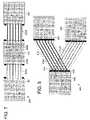
- FIG. 9illustrates a star-type interconnect topology 430 achieved using a pair of direct-connect cable assemblies of FIG. 8 (i.e., assemblies 412 A and 412 B), and the bridging IC 392 of FIG. 7 .
- the bridging IC 392constitutes a hub device of the star topology, and is coupled to each of end-point integrated circuit packages 431 , 432 , 433 and 434 .
- any high-speed interconnect topologymay be implemented using the direct-connect cable assemblies and/or bridging IC described in reference to FIGS. 6 and 7 .
- FIG. 10illustrates an exemplary arrangement of direct-connect signaling paths 485 , 487 , 489 , 491 and 493 established between a number of integrated circuit packages ( 478 , 479 , 480 , 481 and 482 ) mounted on a printed circuit board 477 .
- Numerous other componentsmay be mounted to the printed circuit board 477 and interconnected to one another and/or to the integrated circuit packages 478 - 482 using conventional interconnection structures, or using additional direct-connect cables.
- the direct-connect cables used to establish signaling paths between the integrated circuit packages 478 - 482include straight line cables 485 , 487 and 493 , S-type cable 491 , and elbow cable 489 .
- Integrated circuit package 481may be a bridging IC to establish a through connection between all or a pair of the direct-connect cables 485 , 491 and 493 .
- the direct-connect cables 485 , 491 and 493may each be coupled to distinct sets of I/O circuits within integrated circuit package 481 .
- Integrated circuit packages 480 and 482may similarly be bridging ICs to establish through-connections between direct-connect cables. It should be noted that the direct-connect signaling paths illustrated in FIG.
- direct-connect cablesmay be used to establish connections between integrated circuit packages in a data processing system (e.g., between a general or special-purpose processor and a corresponding chipset component or application specific integrated circuit, or between a memory controller and memory devices and/or memory modules), network switching system (e.g., between integrated circuit packages on one or more line cards, switch fabric cards, etc.), transponder system, high-speed data multiplexing system and so forth.
- a data processing systeme.g., between a general or special-purpose processor and a corresponding chipset component or application specific integrated circuit, or between a memory controller and memory devices and/or memory modules
- network switching systeme.g., between integrated circuit packages on one or more line cards, switch fabric cards, etc.
- transponder systeme.g., between integrated circuit packages on one or more line cards, switch fabric cards, etc.
- FIG. 11illustrates a direct-connect signaling system 500 according to an alternative embodiment of the invention.
- the signaling system 500includes a pair of integrated circuit packages 501 A and 501 B mounted to a printed circuit board 507 and coupled to one another via a direct-connect cable 503 .
- the direct connect cable 503does not include connectors at both ends, but rather is an integral component of integrated circuit package 501 A.
- the direct-connect cable 503is received within an edge of the package substrate 509 (e.g., a concavity formed between the upper and lower surfaces of the package substrate 509 ) and electric signal conductors 502 of the direct-connect cable 503 extend within the substrate 509 (e.g., along the surface of an internal layer of the substrate) to contact a set of vias 504 or other conductive structures coupled to the integrated circuit die 512 .
- the conductors 502 of the direct-connect cable 503may extend along the top surface of the package substrate 509 to contact the die 512 directly (obviating the vias 504 ).
- the conductors 502 of the direct-connect cable 503may extend along the bottom surface of the package substrate 509 and contact the die 512 through vias or other conductive structures disposed within the package substrate 509 .
- the direct connect cable 503may be flexible or rigid, and may be a micro-stripline (i.e., having conductive shield 506 ), coplanar stripline, or non-coplanar cable (e.g., coaxial or other non-coplanar arrangement).
- FIG. 12illustrates a signaling system embodiment 510 that includes integrated circuit packages 511 A, 511 B mounted to printed circuit board 517 and each having an integral direct-connect cable 514 A, 514 B that terminates in a respective mid-span connector 515 A, 515 B.
- the mid-span connectors 515 A and 515 Bare different from one another, with mid-span connector 515 A being adapted to receive protruding contacts of the mid-span connector 515 B (i.e., a male/female connector pair).
- the mid-span connectors 515 A and 515 Bare identical to one another and include latching structures to maintain the respective sets of conductors within the cables 514 A and 514 B in aligned contact with one another.
- the mid-span connectors 515 A and 515 Bmay be permanently or removably coupled to one another.
- conductors within either or both of the direct connect cables 514 A and 514 Bmay extend, in whole or part, within the corresponding package substrate (as shown) or on either surface thereof.
- the direct connect cables 514 A and/or 514 Bmay be flexible or rigid, and may be micro-stripline (i.e., having conductive shield 506 ), coplanar stripline, or non-coplanar cables.
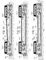
- FIG. 13illustrates a direct-connect signaling system 521 according to another embodiment of the invention.
- the signaling system 521includes integrated circuit packages 522 A and 522 B coupled to on another via a direct-connect cable 523 that rests on a printed circuit board 527 along all or part of its length.
- the direct-connect cable 523is preferably a coplanar structure having a plurality of parallel conductors, but may alternatively be a coaxial or other non-coplanar cable.
- the conductors 525 of the direct-connect cablemay directly contact landings 524 A or other conductive structures on the underside of the package substrate 526 or, as shown in FIG.
- the direct-connect cable 523may be used with conventionally fabricated integrated circuit packages, including the flip-chip packages 522 A, 522 B depicted in FIG. 13 , or integrated circuit packages having leads or other contacts for contacting conductors within the direct-connect cable 523 . While the above-described problems associated with signal redistribution within the integrated circuit package may remain in the embodiment of FIG. 13 , the parasitic capacitance, signal reflections and signal skew associated with PCB routing may be significantly reduced, thereby enabling higher signaling rates and relieving routing congestion in the printed circuit board 527 .
- the conductors 525 of the direct-connect cable 523are preferably electrically isolated from the printed circuit board by a layer of low-loss dielectric material 529 so that conductive traces printed or otherwise formed on the top surface of the printed circuit board 527 may be routed beneath the cable.
- the direct-connect cable 523is preferably flexible to enable the cable to be routed up and over (and/or around) other components mounted on the printed circuit board 527 (e.g., other integrated circuit devices or circuit components disposed between the integrated circuit packages 522 A and 522 B).
- the direct-connect cable 523may be rigid.
- the direct-connect cable 523may be secured to the printed circuit board 527 during system assembly (e.g., using an adhesive or fastener), or allowed to rest unsecured on the printed circuit board 527 .
- FIGS. 14A-14Cillustrate a direct-connect signaling system 530 according to another embodiment of the invention.
- a direct-connect cable 546extends between integrated circuit packages 533 A and 533 B mounted to circuit board 531 , and is secured to each package 533 by a respective one of lid components 535 A and 535 B.
- spring-type contacts 537extend from the direct-connect cable 546 to contact traces disposed on the surface of the package substrates 549 A, 549 B (e.g., as described in reference to FIGS. 4A-4C ).
- Other cable-to-package interconnection structures and techniquesmay be used in alternative embodiments including, without limitation, the contact structures and techniques described above in reference to FIG. 6 .
- the lid component 549is formed from a heat conducting material and includes a heat sinking structure 541 (e.g., fins) disposed in contact with the top surface of the package housing 544 .
- a heat conducting material 539(or adhesive) may be used to improve heat conduction from the integrated circuit package 533 to the lid component 535 .
- the individual conductors 547 of the direct-connect cable 546are routed around openings 548 A and 548 B within the cable 546 that are sized according to the integrated circuit die housing 544 , thereby enabling more direct connection between the package housing 544 and the lid component 535 .
- the openingmay be omitted and the conductors 547 routed directly over the top of the package housing.
- the heat sinking structure 541may be distinct from the lid component 535 or omitted altogether in alternative embodiments (e.g., as shown at 551 of FIG. 14B ), and the lid component 535 may be formed from materials other than heat conducting materials.
- the lid component 535includes protruding members 543 that extend into counterpart holes or slots within package substrate 549 to fasten the lid component 535 to the substrate 549 .
- a lid component 561may alternatively be secured to the package substrate 549 by members 563 that snap about outside edges of the package substrate 549 , securing the lid component 561 against upper and lower surfaces of the substrate 549 .
- the housingmay be omitted, and heat conducting material disposed directly between the integrated circuit die 545 and the lid component 561 . More generally, any mechanism or material for securing the lid 561 (or 535 ) and direct-connect cable 546 to the integrated circuit packages 533 may be used without departing from the spirit and scope of the present invention.
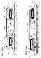
- FIGS. 15A and 15Billustrate a direct-connect signaling system 580 according to another embodiment of the invention.
- direct-connect signaling paths 587 A- 587 Gare disposed in a superstructure 585 that is mounted to a printed circuit board 581 over the top of integrated circuit packages 583 A- 583 N (note that only direct-connect signaling paths 587 A and 587 B are shown in the profile view of FIG. 15B ).
- posts 591are secured to printed circuit board 581 and are received in holes 594 of the superstructure 585 to align the superstructure 585 and printed circuit board 581 .
- Other alignment techniquesmay be used in alternative embodiments.
- the direct-connect signaling paths 587may be formed by conductive traces printed or otherwise disposed on the superstructure 585 , or by securing one or more of the direct-connect cables described in reference to FIGS. 3-14 to a surface of the superstructure 585 .
- contact structures 589are provided to establish contact between terminals 592 of the direct-connect signaling paths and contacts disposed on the substrates of the integrated circuit packages 583 .
- the contact structures 589are depicted as protruding-finger type contacts in FIG. 15B , other types of contact structures may be used including, without limitation, the contact structures described in reference to FIG. 6 . Referring to FIG.
- the direct-connect signaling paths 587 A- 587 Gmay form point-to-point links 587 A, 587 B, 587 C, 587 F and 587 G between integrated circuit packages, as well as multi-drop signaling structures 487 D and 587 E.
- multi-drop structure 587 Eit can be seen that a contact regions 599 is disposed at a point along the length of the signaling path 587 E (i.e., as opposed to at the ends), thereby limiting the stub extending from each contact within contact region 599 to the combined length of the contact structure 589 and package substrate trace.
- mid-span contactsmay be used with other direct-connect cables described herein, thereby establishing multi-drop signaling paths without requiring the bridging IC 382 described in reference to FIG. 7 or cable assembly 412 described in reference to FIG. 8 .
- aperturesmay be provided in superstructure 585 above contact points 592 .
- FIGS. 16A and 16Billustrate direct-connect signaling systems 610 and 625 , respectively, that include leaded integrated circuit packages, instead of or in combination with the flip-chip packages shown in FIGS. 3 and 9 - 12 .
- a direct-connect cable 617extends above leaded integrated circuit packages 613 and 645 and is secured to the integrated circuit packages by sockets 614 and 616 . That is, socket 614 is disposed about integrated circuit package 613 and includes conductive members 618 A that extend from respective cable connection points 612 A to corresponding leads 621 of the integrated circuit package 613 .
- Socket 616is similarly disposed about integrated circuit package 615 and includes conductive members 618 B that extend from respective cable connection points 612 B to corresponding leads 622 of the integrated circuit package 615 . Conductors 619 A- 619 N within the cable extend between respective pairs of contacts 620 with the conductive members 618 .
- the direct connect cable 617is preferably flexible to enable interconnection of the integrated circuit packages 613 and 615 as the packages are disposed at different positions and orientations relative to one another.
- the direct-connect cable 617may be rigid.
- the direct-connect cablemay be a micro-stripline, coplanar stripline, or non-coplanar cable.
- the integrated circuit packages 613 and 615are depicted as being gull-wing-leaded and J-leaded packages, respectively, packages with other types of leads may be used in alternative embodiments.
- a direct-connect cable 635is used to interconnect a flip-chip integrated circuit package 626 and a leaded package 627 .
- the flip-chip package 626is implemented generally as described in reference to FIG. 3 , with conductive traces 629 being routed along a surface of the package substrate 628 to contact zones at an exposed region of the substrate 628 .
- Conductive structures 630are disposed in contact with the traces 629 and extend along the surface of the package housing to a top surface of the housing.
- Contacts 631e.g., solder balls or other structures
- conductive structures 642are similarly extended from the package leads 641 to the top surface of the package housing, where the contacts 643 are used to make electrical connections with the conductors 632 A- 632 N of the direct-connect cable 635 .
- the flip-chip package 626may be coupled to the direct-connect cable 635 using any of the connection techniques and structures described above in reference to FIGS. 3-14 .
- the leaded package 627may be coupled to the direct-connect cable 635 using the socket arrangement described in reference to FIG. 16A .
- the direct-connect superstructure 585 described in reference to FIGS. 15A and 15Bmay be used in place of the discrete direct-connect cables 617 and 635 illustrated in FIGS. 16A and 16B .
- FIGS. 17A-17Fillustrate additional direct-connect signaling system embodiments.
- integrated circuit packages 653 and 657are mounted on distinct printed circuit boards 651 and 655 , respectively, and coupled to one another via a direct-connect cable 659 .
- the printed circuit boards 651 and 655may be arbitrarily positioned with respect to one another and separated by any tolerable signaling distance.
- the printed circuit boards 651 and 655may have additional integrated circuit packages coupled to one another through one or more other-direct connect cables, or in a multi-drop arrangement as described in reference to FIG. 7 .
- the direct-connect cable 659may include multiple sets of conductors as described in reference to FIG. 8 to enable interconnection of multiple integrated circuit packages on the two printed circuit boards 651 and 655 .
- FIG. 17Billustrates a direct-connect signaling system in which an integrated circuit package 663 mounted on a motherboard or backplane 661 is coupled via a direct-connect cable 669 to an integrated circuit package 667 mounted on a daughterboard 665 (i.e., a printed circuit board removably coupled to the motherboard via connector 670 or a similar structure).
- FIG. 17Cillustrates another direct-connect signaling system in which integrated circuit packages 678 and 682 are mounted on respective daughterboards 676 and 680 and coupled to one another via a direct-connect cable 684 .
- the daughterboards 676 and 680are removably inserted into respective connectors 684 and 686 of a backplane or motherboard 675 .
- 17B and 17Cinclude, without limitation, line cards or other cards inserted into a backplane within a network switching apparatus (e.g., switch or router), memory modules inserted into the motherboard or backplane of a computing device or consumer electronic device, and so forth.
- a network switching apparatuse.g., switch or router
- memory modulesinserted into the motherboard or backplane of a computing device or consumer electronic device, and so forth.
- FIG. 17Dillustrates yet another direct-connect signaling system in which integrated packages 697 and 699 are mounted on opposite sides of a printed circuit board 695 or other substrate, and are coupled to one another via a direct-connect cable 700 .
- each of the embodiments depicted in FIGS. 17B-14Dmay include additional integrated circuit packages coupled to one another through direct-connect cables, and the direct-connect cables 669 , 684 and 700 may include multiple sets of connectors as described in reference to FIG. 7 to enable interconnection of multiple integrated circuit packages.
- FIG. 17Eillustrates a signaling system 710 according to another embodiment of the invention.
- the signaling system 710includes a first integrated circuit package 712 mounted to a printed circuit board 711 and coupled to conductors of a direct-connect cable assembly 717 via bond wires 715 or other contact structures. Other bond wires may be used to couple the integrated circuit die to solder balls or other contacts on the underside of the integrated circuit package 712 .
- the direct-connect cable assembly 717includes a lid component 714 having fastening members 716 to secure the assembly 717 to the integrated circuit package 712 .
- the direct-connect cable assemblyalso includes a connector 719 to secure the remote end of the cable assembly 717 to another printed circuit board 721 and to couple the conductors of the cable assembly 717 to traces disposed on the printed circuit board 721 .
- the printed circuit board tracesare coupled to leads (or other contacts) of another integrated circuit package 723 , thereby completing a high-speed signaling path between the integrated circuit packages 712 and 723 .
- the overall high-speed signaling path of system 710is a hybrid path having a direct-connect cable connection to the integrated circuit package 712 , and a conventional connection to integrated circuit package 723 .
- the cable-to-board connector 719may be permanently or removably secured to the printed circuit board 721 .
- integrated circuit package 712may alternatively be any of the types of integrated circuit packages and have any of the cable connections described in reference to FIGS. 3-13 .
- integrated circuit package 723is depicted as a J-lead surface-mount integrated circuit package, any other type of integrated circuit package may be used in alternative embodiments.
- the direct-connect cable assembly 717is depicted as being coupled to only one integrated circuit package 712 , the cable may be coupled to one or more additional packages as described above in reference to FIGS. 6 and 7 .
- the integrated circuit packages 712 and 723may be mounted to the same circuit board rather than the distinct circuit boards 711 and 721 depicted in FIG. 17E .
- FIG. 17Fillustrates a signaling system 730 according another embodiment of the invention.
- the signaling system 730includes a first integrated circuit package 733 mounted to a printed circuit board 731 and coupled to a direct-connect cable 735 .
- the conductors of the direct-connect cable 735are coupled to terminals 738 within an integrated circuit board connector 737 .
- the integrated circuit board connector 737is a socket-style connector adapted to receive an edge connector of a printed circuit board 739 having other components 740 disposed thereon (e.g., a line card, memory module, etc.).
- connector 737may be used in place of connector 737 in alternative embodiments (e.g., pin extensions adapted for insertion into a female connector on a daughterboard), and the direct-connect cable 735 may be permanently or removably coupled to the connector 737 .
- the connector 737may alternatively be mounted on the opposite side of the printed circuit board 731 from the integrated circuit package 733 , or on another printed circuit board altogether.
- the integrated circuit package 733may alternatively be any of the types of integrated circuit packages and have any of the direct-connect cable connections described in reference to FIGS. 3-16 .
- FIGS. 18A-18Dillustrate an exemplary connector system 763 that may be used to establish a direct-connect cable connection between integrated circuit packages 761 A and 761 B, or between an integrated circuit package 761 and a printed circuit board (including a module, such as a memory module).
- connectionis made by a “clam shell” like connector system 763 that aligns and holds fast a transmission cable 760 , with planar in-line or array contacts, to the edge of an interconnection component (e.g., the substrate of an integrated circuit package 761 or printed circuit board or module).
- the clam shell connection system 763includes the following: a top lip of the clam shell connector 773 that is flat (for use where electrical connections are to be made only at a top surface of a substrate); a bottom lip of the clam shell connector 771 that includes a spacer 772 of the thickness of the substrate of the interconnect component 761 ; a flex circuit/transmission cable 760 that carries the electrical signals to and from conductors (shown at 792 in FIG.
- interconnect component 761that makes connection through raised surfaces or protruding structures (i.e., serving as terminals) on either the conductors of the cable 760 or the conductors of the interconnect component 761 ; alignment pins 781 to assure alignment of the direct-connect cable to the contact terminals of the interconnect component 761 and to provide a mechanical anchor and prevent inadvertent pull-off due to shock or vibration; guide pins 775 that allow the top and bottom lips of the connector 771 and 773 to hold alignment to one another as they travel in the z-direction (more or fewer guide pins may be provided in alternative embodiments); springs 777 that urge the connector halves apart for insertion or for removal when removal is required; and a fastening mechanism 779 (e.g., a threaded screw or other closing/force delivery device) that physically clamps the top and bottom lips of the clam shell 771 , 773 against corresponding surfaces of the interconnect component 761 .
- a fastening mechanism 779e.g.,
- the interconnect componente.g., integrated circuit package substrate, printed circuit board or module, etc.
- the interconnect componentincludes recessed areas 785 , such as holes or slots, shaped to receive the alignment pins 781 .
- recessed areas 785such as holes or slots, shaped to receive the alignment pins 781 .
- two alignment pins 781are shown in FIGS. 18B and 18C , more or fewer alignment pins 781 may be provided in alternative embodiments.
- a single alignment holemay be used to establish alignment in the lateral direction along the edge of the interconnect component 761 .
- lengthwise protrusionse.g., fins or blades
- other protrusion geometriesmay be used to establish alignment between the connector system 763 and interconnect component 761 ; the recessed areas 785 (e.g., holes, channels, grooves, etc.) in the interconnect component 761 being shaped according to the protrusion geometry.
- the alignment pins 781may be located on either or both lips 771 and 773 of the connector system 763 .
- the alignment pinsmay alternatively be located on the interconnect component 761 , and the recessed areas 785 on one or both of the lips 771 and 773 .
- the depth of the throat of the connector system 763(i.e., extension of the lips 771 and 773 over the interconnect component 761 ) is not critical but where thinner spacers 772 are used, a shallower throat may improve stiffness.
- the bottom lip of the connector 771does not have to be of the same depth as the top lip 773 and, in one embodiment, is of shallower depth.
- the bottom lip 771may also include alignment pins 781 for more mechanical robustness. Also, as shown in FIG.
- the thickness of the bottom lip 771 of the connectoris reduced to a value less than the anticipated clearance 794 between the package substrate and the printed circuit board 790 (the clearance being determined, at least in part, by the nature of the package-to-board contact 791 ).
- the top and bottom lips of the connector 771 and 773may be formed from any material, and if made of conducting material, may be coupled to a ground reference (e.g., a shield layer) in the cable 760 and/or the interconnect component 761 .
- the alignment pins 781are used to engage a ground reference conductor (or ground plane) and/or supply voltage conductor disposed on or within the interconnect component 761 , thereby establishing a ground and/or power connection.
- alignment between electrical contact points 794 (e.g., pads) disposed on the conductors of cable 760 and corresponding conductors 792 on the interconnect component 761are established by the alignment pins 781 .
- the alignment holes 785 within the interconnect component 761are drilled at specified locations relative to ends of the substrate conductors 792 .
- Through-holes 796 for the alignment pinsare also drilled in the cable 760 at specified locations relative to the cable contacts 794 .
- the cable contacts 794are aligned to contact the ends of the conductors 792 as the connector is closed on the interconnect component 761 .
- the tip of the alignment pins 781may be tapered to enable self-alignment of the pins 781 .
- the structures used to establish electrical contact between the direct-connect cable conductors and the traces 792 on the interconnect component 761may include, but are not limited to, gold dots, nanopierce contacts, pogo-pins, elastomeric pads, micro-springs, plated bumps, particle interconnects, anisotropic conductive films, etc. Coplanarity of the height between different bump contacts, especially for high pin counts, may be achieved using any number of techniques including, without limitation, sandwiching an elastomer between the direct-connect cable and the top lip of the connector, and/or spring loaded contacts 795 behind any bump contact 794 on the direct-connect cable conductors as show in FIG. 18D .
- direct-connect cablesmay be coupled at one end to an integrated circuit package and on the other end to a printed circuit board or to a circuit board (or module) connector.
- direct-connect cablesmay include the connector system 763 described in reference to FIGS. 18A-18D on one end only.
- the other end of the connectormay include a surface mount or mezzanine type connector for connection to a printed circuit board (or module), or may be adapted for connection to contacts of a board or module connector as shown, for example, in FIG. 17F .
- FIGS. 19A and 19Billustrate a direct-connect signaling system according to another embodiment of the invention.
- FIG. 19Ais a top view of an integrated circuit package 820 having multiple integrated circuit dice 823 A and 823 B disposed on a shared package substrate 821 (two dice are shown in FIG. 19A , but any number of dice may be provided in other embodiments).
- MCMsmulti-chip modules
- interconnections between the dice 823are typically made by traces printed one or more layers of the shared substrate 821 .
- MCMsmulti-chip modules
- One drawback to this approachis that, once mounted to the substrate 821 , high-speed testing of an individual die 823 becomes difficult due to the connections to one or more other dice 823 .
- the substrate traces to such other dice 823tend to act as stubs during high-speed signaling tests, degrading signal quality and making tests at run-time frequencies difficult or impossible.
- individual dicemay be tested using wafer-probing techniques, the relatively high inductance of the probes usually prevents testing at run-time frequencies. Consequently, multi-chip modules are often completely assembled, then tested in their integrated form. The problem with this approach is that, if any one of the die within the multi-chip module is defective, the entire multi-chip module is typically discarded.
- many of the testability problems associated with multi-chip modulesare overcome (or at least mitigated) by using a direct-connect cable to establish high-speed links (i.e., signaling paths) between dice.
- a direct-connect cableto establish high-speed links (i.e., signaling paths) between dice.
- FIG. 19Aillustrates a side view of the arrangement in FIG. 19A , showing placement of a direct-connect cable 841 .
- the direct-connect cable 841includes a pair of connectors 843 A, 843 B permanently or removably secured to the contact zones 827 A and 827 B established by respective sets of traces extending from contacts of the integrated circuit dice 823 A and 823 B.
- a high-speed circuit tester(not shown) may be coupled to the corresponding contact zone 827 using a direct-connect test cable (e.g., a cable that corresponds to the cable 841 used to interconnect the package dice 823 ), and tested at run-time frequency. If the die passes the tests, another die may be mounted to the package and similarly tested, with direct-connect cables 841 coupled between pairs or groups of passing dice.
- a diemay be removed from the substrate and replaced by another die. Alternatively, the partially constructed module may be discarded. In either case, individual die may be tested at run-time frequencies without having to complete assembly of the entire multi-chip module.
- the multi-chip module 820 shown in FIGS. 19A and 19Bis a planar style module (i.e., all dice mounted in the same plane, for example, to the surface of a common substrate 821 ), direct-connect cables may also be used to form high-speed signaling paths between dice mounted in different planes of a stacked multi-chip module.
- FIG. 20illustrates a test arrangement that may be used to test circuit-board-mounted integrated circuit packages 879 A and 879 B that are to be interconnected via a direct-connect cable.
- a similar arrangementmay be used to test dice mounted on a substrate of a multi-chip module that are to be interconnected via a direct-connect cable.
- Dashed lines 881illustrate the path of the conductors of the yet-to-be-attached direct-connect connect cable
- 883illustrates the direct-connect cable attachment to a high-speed test apparatus (e.g., an apparatus that generates programmed patterns of test signals). Because the interconnection between the integrated circuit packages 879 A, 879 B is not yet established, package 879 A does not need to be driven to a high impedance state to test 879 B.
- the parasitic capacitance and signal reflections from stub portions of the printed circuit board tracesare avoided, thereby enabling the high-speed test apparatus execute signaling tests at run-time frequencies.
- the direct-connect cable connection to integrated circuit package 879 Bmay be removed, and a direct-connect cable connection to integrated circuit package 879 A established.
- board level integrated circuit package testingmay be executed at run-time frequencies, one integrated circuit package at a time.
- Direct-connect cablesmay be secured between each pair of integrated circuit packages (or group of integrated circuit packages) determined to pass package-level tests.
Landscapes
- Engineering & Computer Science (AREA)
- Microelectronics & Electronic Packaging (AREA)
- Physics & Mathematics (AREA)
- Condensed Matter Physics & Semiconductors (AREA)
- General Physics & Mathematics (AREA)
- Computer Hardware Design (AREA)
- Power Engineering (AREA)
- Manufacturing & Machinery (AREA)
- Combinations Of Printed Boards (AREA)
- Structures Or Materials For Encapsulating Or Coating Semiconductor Devices Or Solid State Devices (AREA)
Abstract
Description
Claims (21)
Priority Applications (3)
| Application Number | Priority Date | Filing Date | Title |
|---|---|---|---|
| US10/426,930US7307293B2 (en) | 2002-04-29 | 2003-04-29 | Direct-connect integrated circuit signaling system for bypassing intra-substrate printed circuit signal paths |
| US11/182,484US7750446B2 (en) | 2002-04-29 | 2005-07-14 | IC package structures having separate circuit interconnection structures and assemblies constructed thereof |
| US11/930,217US7989929B2 (en) | 2002-04-29 | 2007-10-31 | Direct-connect signaling system |
Applications Claiming Priority (3)
| Application Number | Priority Date | Filing Date | Title |
|---|---|---|---|
| US37648202P | 2002-04-29 | 2002-04-29 | |
| US40018002P | 2002-07-31 | 2002-07-31 | |
| US10/426,930US7307293B2 (en) | 2002-04-29 | 2003-04-29 | Direct-connect integrated circuit signaling system for bypassing intra-substrate printed circuit signal paths |
Related Child Applications (2)
| Application Number | Title | Priority Date | Filing Date |
|---|---|---|---|
| US11/182,484Continuation-In-PartUS7750446B2 (en) | 2002-04-29 | 2005-07-14 | IC package structures having separate circuit interconnection structures and assemblies constructed thereof |
| US11/930,217DivisionUS7989929B2 (en) | 2002-04-29 | 2007-10-31 | Direct-connect signaling system |
Publications (2)
| Publication Number | Publication Date |
|---|---|
| US20030222282A1 US20030222282A1 (en) | 2003-12-04 |
| US7307293B2true US7307293B2 (en) | 2007-12-11 |
Family
ID=29406757
Family Applications (2)
| Application Number | Title | Priority Date | Filing Date |
|---|---|---|---|
| US10/426,930Expired - LifetimeUS7307293B2 (en) | 2002-04-29 | 2003-04-29 | Direct-connect integrated circuit signaling system for bypassing intra-substrate printed circuit signal paths |
| US11/930,217Expired - LifetimeUS7989929B2 (en) | 2002-04-29 | 2007-10-31 | Direct-connect signaling system |
Family Applications After (1)
| Application Number | Title | Priority Date | Filing Date |
|---|---|---|---|
| US11/930,217Expired - LifetimeUS7989929B2 (en) | 2002-04-29 | 2007-10-31 | Direct-connect signaling system |
Country Status (6)
| Country | Link |
|---|---|
| US (2) | US7307293B2 (en) |
| EP (1) | EP1506568B1 (en) |
| JP (2) | JP2005524239A (en) |
| CN (1) | CN1659810B (en) |
| AU (1) | AU2003223783A1 (en) |
| WO (1) | WO2003094203A2 (en) |
Cited By (46)
| Publication number | Priority date | Publication date | Assignee | Title |
|---|---|---|---|---|
| US20060226450A1 (en)* | 2005-03-28 | 2006-10-12 | Toyota Jidosha Kabushiki Kaisha | Connecting member used for semiconductor device including plurality of arranged semiconductor modules and semiconductor device provided with the same |
| US20060289981A1 (en)* | 2005-06-28 | 2006-12-28 | Nickerson Robert M | Packaging logic and memory integrated circuits |
| US20070194458A1 (en)* | 2004-07-29 | 2007-08-23 | Watkins Charles M | Methods of redistributing bondpad locations on an integrated circuit |
| US20080036045A1 (en)* | 2006-08-08 | 2008-02-14 | Silicon Base Development Inc. | Package-base structure of power semiconductor device and manufacturing process of the same |
| US20080088009A1 (en)* | 2003-09-08 | 2008-04-17 | Jiangqi He | I/o architecture for integrated circuit package |
| US20080131997A1 (en)* | 2004-03-05 | 2008-06-05 | Joong-Ho Kim | Integrated circuit package with chip-side signal connections |
| US20080176420A1 (en)* | 2007-01-24 | 2008-07-24 | Reuven Weintraub | Device, system, and method of flexible hardware connectivity |
| US20080228821A1 (en)* | 2007-02-22 | 2008-09-18 | Mick Colin K | Method and apparatus for managing a digital inventory of multimedia files stored across a dynamic distributed network |
| US20090302878A1 (en)* | 2006-01-17 | 2009-12-10 | Sherry Jeffrey C | Test Contact System For Testing Integrated Circuits With Packages Having An Array Of Signal and Power Contacts |
| US20100078826A1 (en)* | 2008-09-30 | 2010-04-01 | Charan Gurumurthy | Substrate package with through holes for high speed i/o flex cable |
| US20100208436A1 (en)* | 2007-09-19 | 2010-08-19 | Dieter Cremer | Multilayer Circuit Board and Use of a Multilayer Circuit Board |
| US20100252315A1 (en)* | 2006-06-08 | 2010-10-07 | Chih-Chin Liao | Printed Circuit Board With Coextensive Electrical Connectors And Contact Pad Areas |
| US20100315752A1 (en)* | 2009-06-15 | 2010-12-16 | Stanley Rabu | Thermal protection circuits and structures for electronic devices and cables |
| US20110104940A1 (en)* | 2009-11-03 | 2011-05-05 | Stanley Rabu | Thermal protection circuits for electronic device cables |
| US20120064762A1 (en)* | 2010-09-14 | 2012-03-15 | Fujitsu Limited | Terminal structure of coaxial cable, connector, and substrate unit |
| US20140027157A1 (en)* | 2012-07-26 | 2014-01-30 | Futurewei Technologies, Inc. | Device and Method for Printed Circuit Board with Embedded Cable |
| US20140062516A1 (en)* | 2011-03-21 | 2014-03-06 | University Of Windsor | Apparatus for the Automated Testing and Validation of Electronic Components |
| WO2014108539A1 (en) | 2013-01-11 | 2014-07-17 | Maris Techcon | Optical package and a process for its preparation |
| US9985367B2 (en) | 2013-02-27 | 2018-05-29 | Molex, Llc | High speed bypass cable for use with backplanes |
| US10062984B2 (en) | 2013-09-04 | 2018-08-28 | Molex, Llc | Connector system with cable by-pass |
| US10135211B2 (en) | 2015-01-11 | 2018-11-20 | Molex, Llc | Circuit board bypass assemblies and components therefor |
| USRE47342E1 (en)* | 2009-01-30 | 2019-04-09 | Molex, Llc | High speed bypass cable assembly |
| US20190150311A1 (en)* | 2017-11-13 | 2019-05-16 | Te Connectivity Corporation | Socket connector for an electronic package |
| US10367280B2 (en) | 2015-01-11 | 2019-07-30 | Molex, Llc | Wire to board connectors suitable for use in bypass routing assemblies |
| US10424856B2 (en) | 2016-01-11 | 2019-09-24 | Molex, Llc | Routing assembly and system using same |
| US10424878B2 (en) | 2016-01-11 | 2019-09-24 | Molex, Llc | Cable connector assembly |
| US10720735B2 (en) | 2016-10-19 | 2020-07-21 | Amphenol Corporation | Compliant shield for very high speed, high density electrical interconnection |
| US10739828B2 (en) | 2015-05-04 | 2020-08-11 | Molex, Llc | Computing device using bypass assembly |
| US10840649B2 (en) | 2014-11-12 | 2020-11-17 | Amphenol Corporation | Organizer for a very high speed, high density electrical interconnection system |
| US10931062B2 (en) | 2018-11-21 | 2021-02-23 | Amphenol Corporation | High-frequency electrical connector |
| US11070006B2 (en) | 2017-08-03 | 2021-07-20 | Amphenol Corporation | Connector for low loss interconnection system |
| US11101611B2 (en) | 2019-01-25 | 2021-08-24 | Fci Usa Llc | I/O connector configured for cabled connection to the midboard |
| US11151300B2 (en) | 2016-01-19 | 2021-10-19 | Molex, Llc | Integrated routing assembly and system using same |
| US11189943B2 (en) | 2019-01-25 | 2021-11-30 | Fci Usa Llc | I/O connector configured for cable connection to a midboard |
| US11205877B2 (en) | 2018-04-02 | 2021-12-21 | Ardent Concepts, Inc. | Controlled-impedance compliant cable termination |
| US11437762B2 (en) | 2019-02-22 | 2022-09-06 | Amphenol Corporation | High performance cable connector assembly |
| US11444398B2 (en) | 2018-03-22 | 2022-09-13 | Amphenol Corporation | High density electrical connector |
| US11469554B2 (en) | 2020-01-27 | 2022-10-11 | Fci Usa Llc | High speed, high density direct mate orthogonal connector |
| US11522310B2 (en) | 2012-08-22 | 2022-12-06 | Amphenol Corporation | High-frequency electrical connector |
| US11604219B2 (en) | 2020-12-15 | 2023-03-14 | Teradyne, Inc. | Automatic test equipement having fiber optic connections to remote servers |
| US11670879B2 (en) | 2020-01-28 | 2023-06-06 | Fci Usa Llc | High frequency midboard connector |
| US11735852B2 (en) | 2019-09-19 | 2023-08-22 | Amphenol Corporation | High speed electronic system with midboard cable connector |
| USD1002553S1 (en) | 2021-11-03 | 2023-10-24 | Amphenol Corporation | Gasket for connector |
| US11799246B2 (en) | 2020-01-27 | 2023-10-24 | Fci Usa Llc | High speed connector |
| US11831106B2 (en) | 2016-05-31 | 2023-11-28 | Amphenol Corporation | High performance cable termination |
| US11862901B2 (en) | 2020-12-15 | 2024-01-02 | Teradyne, Inc. | Interposer |
Families Citing this family (102)
| Publication number | Priority date | Publication date | Assignee | Title |
|---|---|---|---|---|
| US7750446B2 (en)* | 2002-04-29 | 2010-07-06 | Interconnect Portfolio Llc | IC package structures having separate circuit interconnection structures and assemblies constructed thereof |
| AU2003223783A1 (en)* | 2002-04-29 | 2003-11-17 | Silicon Pipe, Inc. | Direct-connect signaling system |
| KR100632469B1 (en)* | 2004-04-20 | 2006-10-09 | 삼성전자주식회사 | Semiconductor chip package |
| CN103646848B (en) | 2004-06-04 | 2018-06-05 | 伊利诺伊大学评议会 | The method of assembling printable semiconductor elements and manufacture electronic device |
| US8217381B2 (en)* | 2004-06-04 | 2012-07-10 | The Board Of Trustees Of The University Of Illinois | Controlled buckling structures in semiconductor interconnects and nanomembranes for stretchable electronics |
| US7521292B2 (en) | 2004-06-04 | 2009-04-21 | The Board Of Trustees Of The University Of Illinois | Stretchable form of single crystal silicon for high performance electronics on rubber substrates |
| US7705445B2 (en)* | 2005-02-11 | 2010-04-27 | Rambus Inc. | Semiconductor package with low and high-speed signal paths |
| MY151572A (en)* | 2005-06-02 | 2014-06-13 | Univ Illinois | Printable semiconductor structures and related methods of making and assembling |
| US7518238B2 (en)* | 2005-12-02 | 2009-04-14 | Intel Corporation | Mounting flexible circuits onto integrated circuit substrates |
| US7569916B2 (en)* | 2006-03-14 | 2009-08-04 | Paricon Technologies Corp. | Separable network interconnect systems and assemblies |
| US20080157320A1 (en)* | 2006-12-29 | 2008-07-03 | Harrison Ray D | Laterally Interconnected IC Packages and Methods |
| US7978030B2 (en)* | 2007-02-12 | 2011-07-12 | Finisar Corporation | High-speed interconnects |
| US7859367B2 (en)* | 2007-02-12 | 2010-12-28 | Finisar Corporation | Non-coplanar high-speed interconnects |
| US20080228964A1 (en)* | 2007-03-13 | 2008-09-18 | Henning Braunisch | Hybrid flex-and-board memory interconnect system |
| KR101150454B1 (en)* | 2007-08-06 | 2012-06-01 | 삼성전자주식회사 | Memory module having star-type topology and method of fabricating the same |
| US7880570B2 (en)* | 2007-10-25 | 2011-02-01 | Finisar Corporation | Feed thru with flipped signal plane using guided vias |
| US7671450B2 (en)* | 2007-12-17 | 2010-03-02 | Agere Systems Inc. | Integrated circuit package for high-speed signals |
| TWI723953B (en)* | 2008-03-05 | 2021-04-11 | 美國伊利諾大學理事會 | Stretchable and foldable electronic devices |
| US7517223B1 (en) | 2008-03-21 | 2009-04-14 | Sony Corporation | Controlled impedance bus with a buffer device |
| US7705447B2 (en)* | 2008-09-29 | 2010-04-27 | Intel Corporation | Input/output package architectures, and methods of using same |
| US8097926B2 (en) | 2008-10-07 | 2012-01-17 | Mc10, Inc. | Systems, methods, and devices having stretchable integrated circuitry for sensing and delivering therapy |
| JP5646492B2 (en) | 2008-10-07 | 2014-12-24 | エムシー10 インコーポレイテッドMc10,Inc. | Stretchable integrated circuit and device with sensor array |
| US8389862B2 (en) | 2008-10-07 | 2013-03-05 | Mc10, Inc. | Extremely stretchable electronics |
| US8886334B2 (en) | 2008-10-07 | 2014-11-11 | Mc10, Inc. | Systems, methods, and devices using stretchable or flexible electronics for medical applications |
| US8372726B2 (en) | 2008-10-07 | 2013-02-12 | Mc10, Inc. | Methods and applications of non-planar imaging arrays |
| EP2430652B1 (en) | 2009-05-12 | 2019-11-20 | The Board of Trustees of the University of Illionis | Printed assemblies of ultrathin, microscale inorganic light emitting diodes for deformable and semitransparent displays |
| US9322542B2 (en) | 2009-08-12 | 2016-04-26 | Edward Bryant Stoneham | Versatile sealed LED lamp |
| WO2011041727A1 (en) | 2009-10-01 | 2011-04-07 | Mc10, Inc. | Protective cases with integrated electronics |
| US10918298B2 (en) | 2009-12-16 | 2021-02-16 | The Board Of Trustees Of The University Of Illinois | High-speed, high-resolution electrophysiology in-vivo using conformal electronics |
| US9936574B2 (en) | 2009-12-16 | 2018-04-03 | The Board Of Trustees Of The University Of Illinois | Waterproof stretchable optoelectronics |
| US10441185B2 (en) | 2009-12-16 | 2019-10-15 | The Board Of Trustees Of The University Of Illinois | Flexible and stretchable electronic systems for epidermal electronics |
| KR101729507B1 (en)* | 2010-06-30 | 2017-04-24 | 삼성전자 주식회사 | Printed circuit board unit and computer device having the same |
| KR101443730B1 (en) | 2010-09-18 | 2014-09-23 | 페어차일드 세미컨덕터 코포레이션 | A microelectromechanical die, and a method for making a low-quadrature-error suspension |
| CN103221778B (en) | 2010-09-18 | 2016-03-30 | 快捷半导体公司 | There is single micromechanics one chip three-axis gyroscope driven |
| CN103221779B (en) | 2010-09-18 | 2017-05-31 | 快捷半导体公司 | The axle inertial sensor of micromechanics monoblock type six |
| US9278845B2 (en) | 2010-09-18 | 2016-03-08 | Fairchild Semiconductor Corporation | MEMS multi-axis gyroscope Z-axis electrode structure |
| US9095072B2 (en) | 2010-09-18 | 2015-07-28 | Fairchild Semiconductor Corporation | Multi-die MEMS package |
| WO2012037536A2 (en) | 2010-09-18 | 2012-03-22 | Fairchild Semiconductor Corporation | Packaging to reduce stress on microelectromechanical systems |
| WO2012040211A2 (en) | 2010-09-20 | 2012-03-29 | Fairchild Semiconductor Corporation | Microelectromechanical pressure sensor including reference capacitor |
| US8841560B1 (en)* | 2010-11-17 | 2014-09-23 | Dawn VME Products | Backplane slot interconnection system, method and apparatus |
| CN103609037A (en)* | 2011-04-06 | 2014-02-26 | 华为技术有限公司 | Method for expanding a single chassis network or computing platform using soft interconnects |
| US20120257618A1 (en)* | 2011-04-06 | 2012-10-11 | Futurewei Technologies, Inc. | Method for Expanding a Single Chassis Network or Computing Platform Using Soft Interconnects |
| US9765934B2 (en) | 2011-05-16 | 2017-09-19 | The Board Of Trustees Of The University Of Illinois | Thermally managed LED arrays assembled by printing |
| JP2014523633A (en) | 2011-05-27 | 2014-09-11 | エムシー10 インコーポレイテッド | Electronic, optical and / or mechanical devices and systems and methods of manufacturing these devices and systems |
| WO2012167096A2 (en) | 2011-06-03 | 2012-12-06 | The Board Of Trustees Of The University Of Illinois | Conformable actively multiplexed high-density surface electrode array for brain interfacing |
| US9324678B2 (en) | 2011-12-20 | 2016-04-26 | Intel Corporation | Low profile zero/low insertion force package top side flex cable connector architecture |
| JP5795541B2 (en)* | 2012-01-05 | 2015-10-14 | 株式会社東海理化電機製作所 | Detection signal output device |
| US9062972B2 (en) | 2012-01-31 | 2015-06-23 | Fairchild Semiconductor Corporation | MEMS multi-axis accelerometer electrode structure |
| JP2015521303A (en) | 2012-03-30 | 2015-07-27 | ザ ボード オブ トラスティーズ オブ ザ ユニヴァーシ | An electronic device that can be attached to the surface and can be attached to an accessory |
| US9488693B2 (en) | 2012-04-04 | 2016-11-08 | Fairchild Semiconductor Corporation | Self test of MEMS accelerometer with ASICS integrated capacitors |
| EP2647952B1 (en) | 2012-04-05 | 2017-11-15 | Fairchild Semiconductor Corporation | Mems device automatic-gain control loop for mechanical amplitude drive |
| EP2647955B8 (en) | 2012-04-05 | 2018-12-19 | Fairchild Semiconductor Corporation | MEMS device quadrature phase shift cancellation |
| KR102058489B1 (en) | 2012-04-05 | 2019-12-23 | 페어차일드 세미컨덕터 코포레이션 | Mems device front-end charge amplifier |
| US9625272B2 (en) | 2012-04-12 | 2017-04-18 | Fairchild Semiconductor Corporation | MEMS quadrature cancellation and signal demodulation |
| US8841845B2 (en)* | 2012-07-24 | 2014-09-23 | Ricardo Montemayor | Proximity-based wireless lighting system |
| DE102013014881B4 (en) | 2012-09-12 | 2023-05-04 | Fairchild Semiconductor Corporation | Enhanced silicon via with multi-material fill |
| US9171794B2 (en) | 2012-10-09 | 2015-10-27 | Mc10, Inc. | Embedding thin chips in polymer |
| JP2014096667A (en)* | 2012-11-08 | 2014-05-22 | Murata Mfg Co Ltd | Module |
| TWI518868B (en) | 2013-02-05 | 2016-01-21 | 聯詠科技股份有限公司 | Integrated circuit |
| CN103996677B (en)* | 2013-02-19 | 2016-12-28 | 联咏科技股份有限公司 | integrated circuit |
| US9837191B2 (en)* | 2014-01-02 | 2017-12-05 | Raytheon Company | Method of connecting an additive communication cable to an electrical harness |
| EP3125656B1 (en)* | 2014-03-26 | 2020-02-19 | Panasonic Intellectual Property Management Co., Ltd. | Electronic device and display unit |
| US10451652B2 (en)* | 2014-07-16 | 2019-10-22 | Teradyne, Inc. | Coaxial structure for transmission of signals in test equipment |
| US10297572B2 (en)* | 2014-10-06 | 2019-05-21 | Mc10, Inc. | Discrete flexible interconnects for modules of integrated circuits |
| AU2016270807A1 (en) | 2015-06-01 | 2017-12-14 | The Board Of Trustees Of The University Of Illinois | Miniaturized electronic systems with wireless power and near-field communication capabilities |
| MX2017015587A (en) | 2015-06-01 | 2018-08-23 | Univ Illinois | Alternative approach to uv sensing. |
| US12189195B2 (en) | 2015-10-08 | 2025-01-07 | Teramount Ltd. | Optical coupling |
| US11585991B2 (en) | 2019-02-28 | 2023-02-21 | Teramount Ltd. | Fiberless co-packaged optics |
| US12379555B2 (en)* | 2021-10-27 | 2025-08-05 | Teramount Ltd. | Detachable connector for co-packaged optics |
| US12265259B2 (en) | 2019-01-23 | 2025-04-01 | Teramount Ltd. | Waveguide mode coupling |
| US12164159B2 (en) | 2021-12-22 | 2024-12-10 | Teramount Ltd. | Backside optical connector |
| US12124087B2 (en) | 2015-10-08 | 2024-10-22 | Teramount Ltd. | Wideband surface coupling |
| KR102497583B1 (en)* | 2015-10-27 | 2023-02-10 | 삼성전자주식회사 | Semiconductor devices having flexible interconnection and methods for fabricating the same |
| US10312967B2 (en)* | 2015-12-15 | 2019-06-04 | Nvidia Corporation | System and method for cross-talk cancellation in single-ended signaling |
| CN109691244B (en)* | 2016-09-19 | 2022-07-19 | 英特尔公司 | Alternate circuit arrangement and method for long host routing |
| WO2018124004A1 (en)* | 2016-12-28 | 2018-07-05 | 株式会社村田製作所 | Electronic device |
| CN214754244U (en)* | 2017-02-03 | 2021-11-16 | 株式会社村田制作所 | Interposer and electronic apparatus |
| US10044155B1 (en)* | 2017-05-10 | 2018-08-07 | Qualcomm Incorporated | Connector for connecting a device to a plurality of pads arranged at different radial distances from the source |
| US20190051587A1 (en)* | 2017-08-11 | 2019-02-14 | Marvell Israel (M.I.S.L) Ltd. | Ic package |
| FR3070573A1 (en) | 2017-08-25 | 2019-03-01 | Stmicroelectronics (Grenoble 2) Sas | ELECTRONIC DEVICE INCLUDING AT LEAST ONE ELECTRONIC CHIP AND ELECTRONIC ASSEMBLY |
| TWI833717B (en)* | 2017-11-14 | 2024-03-01 | 美商山姆科技公司 | Connector, data communication system, method of mounting connector, electrical component and method of constructing electrical component |
| US11508663B2 (en) | 2018-02-02 | 2022-11-22 | Marvell Israel (M.I.S.L) Ltd. | PCB module on package |
| WO2019178619A1 (en)* | 2018-03-16 | 2019-09-19 | Samtec, Inc. | Multiple circuit boards with high-density compression interconnect |
| CN208797213U (en)* | 2018-06-08 | 2019-04-26 | 安费诺电子装配(厦门)有限公司 | A kind of line-end connector and connector assembly of band rotation locking bar |
| US10716213B2 (en) | 2018-07-28 | 2020-07-14 | Hewlett Packard Enterprise Development Lp | Direct connection of high speed signals on PCB chip |
| CN209016312U (en) | 2018-07-31 | 2019-06-21 | 安费诺电子装配(厦门)有限公司 | A kind of line-end connector and connector assembly |
| CN111367727B (en) | 2018-12-25 | 2023-11-17 | 中兴通讯股份有限公司 | Connector structure, and method and device for calculating time delay difference |
| WO2020172743A1 (en)* | 2019-02-25 | 2020-09-03 | Reflex Photonics Inc. | Method and assembly for board to board connection of active devices |
| CN109856499A (en)* | 2019-03-22 | 2019-06-07 | 京东方科技集团股份有限公司 | A kind of driving part and its detection method, display device |
| WO2020250162A1 (en) | 2019-06-10 | 2020-12-17 | Marvell Israel (M.I.S.L) Ltd. | Ic package with top-side memory module |
| US11552432B2 (en)* | 2019-08-12 | 2023-01-10 | High Speed Interconnects, Llc | Methods and apparatus for RF shield and cable attachment system |
| US20220313069A1 (en)* | 2019-08-12 | 2022-10-06 | High Speed Interconnects, Llc | Systems and Methods for Application of Rigid and Flexible Adhesives for Cable Attachment to BGAs |
| US20190387634A1 (en)* | 2019-08-29 | 2019-12-19 | Intel Corporation | System, apparatus and method for providing a symmetric multi-processor high-speed link |
| US11282806B2 (en)* | 2019-10-11 | 2022-03-22 | Marvell Asia Pte, Ltd. | Partitioned substrates with interconnect bridge |
| CN113424198B (en)* | 2019-11-15 | 2023-08-29 | 昆仑芯(北京)科技有限公司 | Distributed AI training topology based on flexible cable connection |
| CN114121873B (en)* | 2020-08-25 | 2025-05-27 | 美光科技公司 | Apparatus and systems with ball grid arrays and related microelectronic devices and device packages |
| WO2022226873A1 (en)* | 2021-04-29 | 2022-11-03 | 华为技术有限公司 | Circuit board assembly part and electronic device |
| CN115426541A (en)* | 2021-05-17 | 2022-12-02 | 华为技术有限公司 | Electronic components, switches and computer systems |
| US12328811B2 (en)* | 2021-07-27 | 2025-06-10 | Samsung Electronics Co., Ltd | Insulating member arrangement structure and electronic device including the same |
| US12243855B2 (en)* | 2021-11-22 | 2025-03-04 | Qualcomm Incorporated | Package comprising channel interconnects located between solder interconnects |
| TWI818458B (en)* | 2022-03-04 | 2023-10-11 | 矽品精密工業股份有限公司 | Electronic package and manufacturing method thereof |
| US12438114B2 (en) | 2022-03-18 | 2025-10-07 | Meta Platforms, Inc. | Flex bonded integrated circuits |
Citations (110)
| Publication number | Priority date | Publication date | Assignee | Title |
|---|---|---|---|---|
| US3795845A (en) | 1972-12-26 | 1974-03-05 | Ibm | Semiconductor chip having connecting pads arranged in a non-orthogonal array |
| US4095866A (en) | 1977-05-19 | 1978-06-20 | Ncr Corporation | High density printed circuit board and edge connector assembly |
| US4202007A (en) | 1978-06-23 | 1980-05-06 | International Business Machines Corporation | Multi-layer dielectric planar structure having an internal conductor pattern characterized with opposite terminations disposed at a common edge surface of the layers |
| US4302501A (en) | 1975-12-24 | 1981-11-24 | Koreyuki Nagashima | Porous, heat resistant insulating substrates for use in printed circuit boards, printed circuit boards utilizing the same and method of manufacturing insulating substrates and printed circuit boards |
| US4445735A (en) | 1980-12-05 | 1984-05-01 | Compagnie Internationale Pour L'informatique Cii-Honeywell Bull (Societe Anonyme) | Electrical connection device for high density contacts |
| US4458297A (en) | 1981-01-16 | 1984-07-03 | Mosaic Systems, Inc. | Universal interconnection substrate |
| US4543715A (en) | 1983-02-28 | 1985-10-01 | Allied Corporation | Method of forming vertical traces on printed circuit board |
| US4551673A (en) | 1980-10-13 | 1985-11-05 | Riba-Pruftechnik Gmbh | Testing arrangement for printed circuit boards |
| US4636919A (en) | 1985-03-20 | 1987-01-13 | Hitachi, Ltd. | Multilayer printed circuit board |
| US4644092A (en)* | 1985-07-18 | 1987-02-17 | Amp Incorporated | Shielded flexible cable |
| US4675243A (en) | 1983-02-25 | 1987-06-23 | Shinko Electric Industries Co., Ltd. | Ceramic package for semiconductor devices |
| US4730159A (en) | 1984-06-21 | 1988-03-08 | The General Electric Company P.L.C. | Programmable bed-of-nails test access jigs |
| US4731643A (en) | 1985-10-21 | 1988-03-15 | International Business Machines Corporation | Logic-circuit layout for large-scale integrated circuits |
| US4748495A (en) | 1985-08-08 | 1988-05-31 | Dypax Systems Corporation | High density multi-chip interconnection and cooling package |
| US4768154A (en) | 1987-05-08 | 1988-08-30 | Telesis Systems Corporation | Computer aided printed circuit board wiring |
| US4799617A (en) | 1987-10-09 | 1989-01-24 | Advanced Techniques Co., Inc. | Convection heat attachment and removal instrument for surface mounted assemblies |
| US4812792A (en) | 1983-12-22 | 1989-03-14 | Trw Inc. | High-frequency multilayer printed circuit board |
| US4814945A (en) | 1987-09-18 | 1989-03-21 | Trw Inc. | Multilayer printed circuit board for ceramic chip carriers |
| US4838800A (en) | 1988-05-23 | 1989-06-13 | Gte Products Corporation | High density interconnect system |
| US4861251A (en) | 1988-02-29 | 1989-08-29 | Diehard Engineering, Inc. | Apparatus for encapsulating selected portions of a printed circuit board |
| US4881905A (en) | 1986-05-23 | 1989-11-21 | Amp Incorporated | High density controlled impedance connector |
| US4912603A (en) | 1985-12-09 | 1990-03-27 | Fujitsu Limited | High density printed wiring board |
| US4935584A (en) | 1988-05-24 | 1990-06-19 | Tektronix, Inc. | Method of fabricating a printed circuit board and the PCB produced |
| US4956749A (en) | 1987-11-20 | 1990-09-11 | Hewlett-Packard Company | Interconnect structure for integrated circuits |
| US4960386A (en) | 1989-10-17 | 1990-10-02 | Molex Incorporated | High deflection, high density single sided electrical connector |
| US4969826A (en) | 1989-12-06 | 1990-11-13 | Amp Incorporated | High density connector for an IC chip carrier |
| US4982311A (en) | 1987-09-29 | 1991-01-01 | Bull S.A. | Package for very large scale integrated circuit |
| US4991115A (en) | 1989-05-16 | 1991-02-05 | Excellon Industries, Inc. | Method of mapping geometric entities from a continuous plane to a discrete plane |
| US4994938A (en) | 1988-12-28 | 1991-02-19 | Texas Instruments Incorporated | Mounting of high density components on substrate |
| US5009611A (en) | 1990-05-23 | 1991-04-23 | Molex Incorporated | High density electrical connector for printed circuit boards |
| US5012924A (en) | 1990-03-19 | 1991-05-07 | R. H. Murphy Company, Inc. | Carriers for integrated circuits and the like |
| US5019946A (en) | 1988-09-27 | 1991-05-28 | General Electric Company | High density interconnect with high volumetric efficiency |
| US5136123A (en) | 1987-07-17 | 1992-08-04 | Junkosha Co., Ltd. | Multilayer circuit board |
| US5155577A (en) | 1991-01-07 | 1992-10-13 | International Business Machines Corporation | Integrated circuit carriers and a method for making engineering changes in said carriers |
| US5162792A (en) | 1990-08-03 | 1992-11-10 | American Telephone And Telegraph Company | On-the-fly arrangement for interconnecting leads and connectors |
| US5165984A (en) | 1991-07-30 | 1992-11-24 | At&T Bell Laboratories | Stepped multilayer interconnection apparatus and method of making the same |
| US5185502A (en) | 1989-12-01 | 1993-02-09 | Cray Research, Inc. | High power, high density interconnect apparatus for integrated circuits |
| US5220490A (en) | 1990-10-25 | 1993-06-15 | Microelectronics And Computer Technology Corporation | Substrate interconnect allowing personalization using spot surface links |
| US5222014A (en) | 1992-03-02 | 1993-06-22 | Motorola, Inc. | Three-dimensional multi-chip pad array carrier |
| US5227013A (en) | 1991-07-25 | 1993-07-13 | Microelectronics And Computer Technology Corporation | Forming via holes in a multilevel substrate in a single step |
| US5291375A (en) | 1991-09-30 | 1994-03-01 | Kabushiki Kaisha Toshiba | Printed circuit board and electric device configured to facilitate bonding |
| US5309324A (en) | 1991-11-26 | 1994-05-03 | Herandez Jorge M | Device for interconnecting integrated circuit packages to circuit boards |
| US5319224A (en) | 1989-10-11 | 1994-06-07 | Mitsubishi Denki Kabushiki Kaisha | Integrated circuit device having a geometry to enhance fabrication and testing and manufacturing method thereof |
| US5417577A (en) | 1992-09-23 | 1995-05-23 | At&T Corp. | Interconnection method and apparatus |
| US5424492A (en) | 1994-01-06 | 1995-06-13 | Dell Usa, L.P. | Optimal PCB routing methodology for high I/O density interconnect devices |
| US5441917A (en) | 1992-07-17 | 1995-08-15 | Lsi Logic Corporation | Method of laying out bond pads on a semiconductor die |
| US5490040A (en) | 1993-12-22 | 1996-02-06 | International Business Machines Corporation | Surface mount chip package having an array of solder ball contacts arranged in a circle and conductive pin contacts arranged outside the circular array |
| US5491364A (en) | 1994-08-31 | 1996-02-13 | Delco Electronics Corporation | Reduced stress terminal pattern for integrated circuit devices and packages |
| US5498767A (en) | 1994-10-11 | 1996-03-12 | Motorola, Inc. | Method for positioning bond pads in a semiconductor die layout |
| US5500862A (en) | 1993-10-29 | 1996-03-19 | Nec Corporation | Multi-layer digital circuit board with a test pattern section |
| US5544018A (en) | 1994-04-13 | 1996-08-06 | Microelectronics And Computer Technology Corporation | Electrical interconnect device with customizeable surface layer and interwoven signal lines |
| US5545301A (en) | 1993-04-23 | 1996-08-13 | Robert Bosch Gmbh | Sensor element for the determination of concentration of gas constituent(s) |
| US5565706A (en)* | 1994-03-18 | 1996-10-15 | Hitachi, Ltd. | LSI package board |
| US5578870A (en) | 1995-08-03 | 1996-11-26 | Precision Connector Designs, Inc. | Top loading test socket for ball grid arrays |
| US5584721A (en) | 1993-01-13 | 1996-12-17 | Sumitomo Wiring Systems, Ltd. | Connector |
| US5587944A (en) | 1996-03-18 | 1996-12-24 | Motorola | High density multistate SRAM and cell |
| US5596205A (en) | 1993-07-12 | 1997-01-21 | Peregrine Semiconductor Corporation | High-frequency wireless communication system on a single ultrathin silicon on sapphire chip |
| US5634093A (en) | 1991-01-30 | 1997-05-27 | Kabushiki Kaisha Toshiba | Method and CAD system for designing wiring patterns using predetermined rules |
| US5644500A (en) | 1994-03-18 | 1997-07-01 | Fujitsu Limited | Routing program generating method and apparatus therefor, placement program generating method and apparatus therefor, and automatic routing method and apparatus therefor |
| US5684332A (en) | 1994-05-27 | 1997-11-04 | Advanced Semiconductor Engineering, Inc. | Method of packaging a semiconductor device with minimum bonding pad pitch and packaged device therefrom |
| US5686699A (en) | 1995-10-10 | 1997-11-11 | Acc Microelectronics Corporation | Semiconductor board providing high signal pin utilization |
| US5691569A (en) | 1995-12-20 | 1997-11-25 | Intel Corporation | Integrated circuit package that has a plurality of staggered pins |
| US5701233A (en)* | 1995-01-23 | 1997-12-23 | Irvine Sensors Corporation | Stackable modules and multimodular assemblies |
| US5706178A (en) | 1995-12-20 | 1998-01-06 | Intel Corporation | Ball grid array integrated circuit package that has vias located within the solder pads of a package |
| US5715274A (en) | 1995-01-09 | 1998-02-03 | Lsi Logic Corporation | Method and system for communicating between a plurality of semiconductor devices |
| US5723906A (en)* | 1996-06-07 | 1998-03-03 | Hewlett-Packard Company | High-density wirebond chip interconnect for multi-chip modules |
| US5729432A (en) | 1995-07-05 | 1998-03-17 | Anam Industrial Col, Ltd. | Ball grid array semiconductor package with improved heat dissipation and dehumidification effect |
| US5730606A (en) | 1996-04-02 | 1998-03-24 | Aries Electronics, Inc. | Universal production ball grid array socket |
| US5745374A (en) | 1994-07-22 | 1998-04-28 | Kabushiki Kaisha Toshiba | Layout method for semiconductor integrated circuit and layout apparatus for semiconductor integrated circuit |
| US5774340A (en) | 1996-08-28 | 1998-06-30 | International Business Machines Corporation | Planar redistribution structure and printed wiring device |
| US5781446A (en) | 1996-05-07 | 1998-07-14 | Flexible Solutions, Inc. | System and method for multi-constraint domain electronic system design mapping |
| US5784262A (en) | 1995-11-06 | 1998-07-21 | Symbios, Inc. | Arrangement of pads and through-holes for semiconductor packages |
| US5784264A (en) | 1994-11-28 | 1998-07-21 | Nec Corporation | MCM (Multi Chip Module) carrier with external connection teminals BGA (Ball Grid Array) type matrix array form |
| US5786631A (en) | 1995-10-04 | 1998-07-28 | Lsi Logic Corporation | Configurable ball grid array package |
| US5790383A (en) | 1996-02-20 | 1998-08-04 | Canon Kabushiki Kaisha | Printed circuit board |
| US5819403A (en) | 1994-03-11 | 1998-10-13 | The Panda Project | Method of manufacturing a semiconductor chip carrier |
| US5822214A (en) | 1994-11-02 | 1998-10-13 | Lsi Logic Corporation | CAD for hexagonal architecture |
| US5977640A (en) | 1998-06-26 | 1999-11-02 | International Business Machines Corporation | Highly integrated chip-on-chip packaging |
| US6060772A (en)* | 1997-06-30 | 2000-05-09 | Kabushiki Kaisha Toshiba | Power semiconductor module with a plurality of semiconductor chips |
| US6087732A (en) | 1998-09-28 | 2000-07-11 | Lucent Technologies, Inc. | Bond pad for a flip-chip package |
| US6121679A (en) | 1998-03-10 | 2000-09-19 | Luvara; John J. | Structure for printed circuit design |
| US6137064A (en) | 1999-06-11 | 2000-10-24 | Teradyne, Inc. | Split via surface mount connector and related techniques |
| US6150729A (en) | 1999-07-01 | 2000-11-21 | Lsi Logic Corporation | Routing density enhancement for semiconductor BGA packages and printed wiring boards |
| US6181718B1 (en)* | 1997-01-08 | 2001-01-30 | Matsushita Electric Industrial Co., Ltd. | Electronically cooled semiconductor laser module with modified ground line inductance |
| US6264476B1 (en) | 1999-12-09 | 2001-07-24 | High Connection Density, Inc. | Wire segment based interposer for high frequency electrical connection |
| US6285560B1 (en) | 1999-09-20 | 2001-09-04 | Texas Instruments Incorporated | Method for increasing device reliability by selectively depopulating solder balls from a foot print of a ball grid array (BGA) package, and device so modified |
| US6304450B1 (en) | 1999-07-15 | 2001-10-16 | Incep Technologies, Inc. | Inter-circuit encapsulated packaging |
| US6310398B1 (en) | 1998-12-03 | 2001-10-30 | Walter M. Katz | Routable high-density interfaces for integrated circuit devices |
| US6310303B1 (en) | 1998-03-10 | 2001-10-30 | John J. Luvara | Structure for printed circuit design |
| US6388208B1 (en) | 1999-06-11 | 2002-05-14 | Teradyne, Inc. | Multi-connection via with electrically isolated segments |
| US6465336B2 (en)* | 1997-04-09 | 2002-10-15 | Agere Systems Guardian Corp. | Circuit and method for providing interconnections among individual integrated circuit chips in a multi-chip module |
| US6507496B2 (en) | 2001-05-31 | 2003-01-14 | Intel Corporation | Module having integrated circuit packages coupled to multiple sides with package types selected based on inductance of leads to couple the module to another component |
| US20030048998A1 (en)* | 2001-09-12 | 2003-03-13 | Yuan-Liang Li | Optical/electrical interconnects and package for high speed signaling |
| US6547570B2 (en) | 1998-06-23 | 2003-04-15 | Intel Corporation | IC package with quick connect feature |
| US6559531B1 (en) | 1999-10-14 | 2003-05-06 | Sun Microsystems, Inc. | Face to face chips |
| US6603077B2 (en)* | 2000-12-22 | 2003-08-05 | Canon Kabushiki Kaisha | Cable connection structure and electronic apparatus having the same |
| US20030180006A1 (en)* | 2002-03-22 | 2003-09-25 | Ban-Poh Loh | Waveguide based optical coupling of a fiber optic cable and an optoelectronic device |
| US6642808B2 (en)* | 2000-05-30 | 2003-11-04 | Kyocera Corporation | High frequency package, wiring board, and high frequency module having a cyclically varying transmission characteristic |
| US6686666B2 (en) | 2002-05-16 | 2004-02-03 | Intel Corporation | Breaking out signals from an integrated circuit footprint |
| US6704204B1 (en) | 1998-06-23 | 2004-03-09 | Intel Corporation | IC package with edge connect contacts |
| US20040094328A1 (en)* | 2002-11-16 | 2004-05-20 | Fjelstad Joseph C. | Cabled signaling system and components thereof |
| US20040113250A1 (en)* | 2002-12-12 | 2004-06-17 | Khandros Igor Y. | Integrated circuit assembly |
| US6797891B1 (en)* | 2002-03-18 | 2004-09-28 | Applied Micro Circuits Corporation | Flexible interconnect cable with high frequency electrical transmission line |
| US6867668B1 (en)* | 2002-03-18 | 2005-03-15 | Applied Micro Circuits Corporation | High frequency signal transmission from the surface of a circuit substrate to a flexible interconnect cable |
| US6882546B2 (en)* | 2001-10-03 | 2005-04-19 | Formfactor, Inc. | Multiple die interconnect system |
| US20050087356A1 (en)* | 2002-11-08 | 2005-04-28 | Robert Forcier | Build-up structures with multi-angle vias for chip to chip interconnects and optical bussing |
| US6893885B2 (en)* | 2002-01-18 | 2005-05-17 | The Regents Of The University Of Michigan | Method for electrically and mechanically connecting microstructures using solder |
| US20050133929A1 (en)* | 2003-12-18 | 2005-06-23 | Howard Gregory E. | Flexible package with rigid substrate segments for high density integrated circuit systems |
| US6985659B2 (en)* | 2003-06-30 | 2006-01-10 | Opnext Japan, Inc. | Optical transmission module |
| US20060091507A1 (en)* | 2002-04-29 | 2006-05-04 | Fjelstad Joseph C | IC package structures having separate circuit interconnection structures and assemblies constructed thereof |
Family Cites Families (25)
| Publication number | Priority date | Publication date | Assignee | Title |
|---|---|---|---|---|
| US4543713A (en)* | 1983-08-08 | 1985-10-01 | At&T Technologies, Inc. | Technique for inserting connector leads into a circuit board |
| JPS61287253A (en)* | 1985-06-14 | 1986-12-17 | Hitachi Ltd | Semiconductor device |
| FR2616503B1 (en)* | 1987-06-11 | 1992-07-10 | Ferco Int Usine Ferrures | DOUBLE ACTION SHOCK ABSORBER CAUSING LAMINATION OF A FLUID ON THE PASSAGE OF A THREAD |
| US5135123A (en)* | 1990-09-20 | 1992-08-04 | Phoenix Closures, Inc. | Tamper-evident closure with a separately formed break away band |
| JPH0536857A (en)* | 1991-07-30 | 1993-02-12 | Toshiba Corp | Semiconductor integrated circuit mounting board |
| JPH0730224A (en)* | 1991-12-02 | 1995-01-31 | Nippon Telegr & Teleph Corp <Ntt> | Electronic device mounting structure |
| US5306162A (en)* | 1993-04-14 | 1994-04-26 | Compaq Computer Corporation | Clamp connector apparatus for removably coupling a flexible ribbon cable to a printed circuit board |
| US5343074A (en)* | 1993-10-04 | 1994-08-30 | Motorola, Inc. | Semiconductor device having voltage distribution ring(s) and method for making the same |
| DE69624257T2 (en)* | 1995-11-27 | 2003-09-18 | Kaneka Corp., Osaka | METHOD FOR PRODUCING POLYMERS WITH FUNCTIONAL GROUPS |
| US6361794B1 (en)* | 1996-06-12 | 2002-03-26 | Basf Corporation | Method of making ibuprofen and narcotic analgesic composition |
| US5715724A (en)* | 1996-09-03 | 1998-02-10 | Chambersburg Engineering Company | Adaptive, self-regulating forging hammer control system |
| US5926714A (en)* | 1996-12-03 | 1999-07-20 | Advanced Micro Devices, Inc. | Detached drain MOSFET |
| US6230450B1 (en)* | 1996-12-27 | 2001-05-15 | Sumitomo Construction Co., Ltd. | Damping top, damping rod, and damping device using same |
| JPH10270496A (en)* | 1997-03-27 | 1998-10-09 | Hitachi Ltd | Electronic device, information processing device, semiconductor device, and semiconductor chip mounting method |
| JPH1168031A (en)* | 1997-08-11 | 1999-03-09 | Mitsubishi Electric Corp | IC modules and semiconductor components |
| JPH11340601A (en)* | 1998-05-25 | 1999-12-10 | Fujikura Ltd | Optical element mounting method and flexible printed wiring board |
| JP2000091751A (en)* | 1998-09-10 | 2000-03-31 | Toyo Commun Equip Co Ltd | High-frequency circuit using laminated board |
| JP3767246B2 (en)* | 1999-05-26 | 2006-04-19 | 富士通株式会社 | Composite module and printed circuit board unit |
| JP2001185648A (en)* | 1999-12-24 | 2001-07-06 | Mitsubishi Electric Corp | Semiconductor device |
| JP2001244409A (en)* | 2000-02-29 | 2001-09-07 | Kyocera Corp | High frequency module |
| JP4215378B2 (en)* | 2000-06-05 | 2009-01-28 | 新光電気工業株式会社 | Electronic component mounting carrier, electronic component mounting method, and semiconductor device |
| JP2003039331A (en)* | 2001-08-01 | 2003-02-13 | Noritake Co Ltd | Grinding wheel having resin core part, manufacturing method thereof, and recycling method thereof |
| US6882034B2 (en)* | 2001-08-29 | 2005-04-19 | Micron Technology, Inc. | Routing element for use in multi-chip modules, multi-chip modules including the routing element, and methods |
| AU2003223783A1 (en)* | 2002-04-29 | 2003-11-17 | Silicon Pipe, Inc. | Direct-connect signaling system |
| US6839885B2 (en)* | 2002-08-22 | 2005-01-04 | Agilent Technologies, Inc. | Determining via placement in the printed circuit board of a wireless test fixture |
- 2003
- 2003-04-29AUAU2003223783Apatent/AU2003223783A1/ennot_activeAbandoned
- 2003-04-29USUS10/426,930patent/US7307293B2/ennot_activeExpired - Lifetime
- 2003-04-29WOPCT/US2003/013524patent/WO2003094203A2/enactiveApplication Filing
- 2003-04-29JPJP2004502330Apatent/JP2005524239A/ennot_activeWithdrawn
- 2003-04-29CNCN038137585Apatent/CN1659810B/ennot_activeExpired - Lifetime
- 2003-04-29EPEP03719987.4Apatent/EP1506568B1/ennot_activeExpired - Lifetime
- 2007
- 2007-10-31USUS11/930,217patent/US7989929B2/ennot_activeExpired - Lifetime
- 2010
- 2010-04-08JPJP2010089212Apatent/JP5437137B2/ennot_activeExpired - Fee Related
Patent Citations (113)
| Publication number | Priority date | Publication date | Assignee | Title |
|---|---|---|---|---|
| US3795845A (en) | 1972-12-26 | 1974-03-05 | Ibm | Semiconductor chip having connecting pads arranged in a non-orthogonal array |
| US4302501A (en) | 1975-12-24 | 1981-11-24 | Koreyuki Nagashima | Porous, heat resistant insulating substrates for use in printed circuit boards, printed circuit boards utilizing the same and method of manufacturing insulating substrates and printed circuit boards |
| US4095866A (en) | 1977-05-19 | 1978-06-20 | Ncr Corporation | High density printed circuit board and edge connector assembly |
| US4202007A (en) | 1978-06-23 | 1980-05-06 | International Business Machines Corporation | Multi-layer dielectric planar structure having an internal conductor pattern characterized with opposite terminations disposed at a common edge surface of the layers |
| US4551673A (en) | 1980-10-13 | 1985-11-05 | Riba-Pruftechnik Gmbh | Testing arrangement for printed circuit boards |
| US4445735A (en) | 1980-12-05 | 1984-05-01 | Compagnie Internationale Pour L'informatique Cii-Honeywell Bull (Societe Anonyme) | Electrical connection device for high density contacts |
| US4458297A (en) | 1981-01-16 | 1984-07-03 | Mosaic Systems, Inc. | Universal interconnection substrate |
| US4675243A (en) | 1983-02-25 | 1987-06-23 | Shinko Electric Industries Co., Ltd. | Ceramic package for semiconductor devices |
| US4543715A (en) | 1983-02-28 | 1985-10-01 | Allied Corporation | Method of forming vertical traces on printed circuit board |
| US4812792A (en) | 1983-12-22 | 1989-03-14 | Trw Inc. | High-frequency multilayer printed circuit board |
| US4730159A (en) | 1984-06-21 | 1988-03-08 | The General Electric Company P.L.C. | Programmable bed-of-nails test access jigs |
| US4636919A (en) | 1985-03-20 | 1987-01-13 | Hitachi, Ltd. | Multilayer printed circuit board |
| US4644092A (en)* | 1985-07-18 | 1987-02-17 | Amp Incorporated | Shielded flexible cable |
| US4748495A (en) | 1985-08-08 | 1988-05-31 | Dypax Systems Corporation | High density multi-chip interconnection and cooling package |
| US4731643A (en) | 1985-10-21 | 1988-03-15 | International Business Machines Corporation | Logic-circuit layout for large-scale integrated circuits |
| US4912603A (en) | 1985-12-09 | 1990-03-27 | Fujitsu Limited | High density printed wiring board |
| US4881905A (en) | 1986-05-23 | 1989-11-21 | Amp Incorporated | High density controlled impedance connector |
| US4768154A (en) | 1987-05-08 | 1988-08-30 | Telesis Systems Corporation | Computer aided printed circuit board wiring |
| US5136123A (en) | 1987-07-17 | 1992-08-04 | Junkosha Co., Ltd. | Multilayer circuit board |
| US4814945A (en) | 1987-09-18 | 1989-03-21 | Trw Inc. | Multilayer printed circuit board for ceramic chip carriers |
| US4982311A (en) | 1987-09-29 | 1991-01-01 | Bull S.A. | Package for very large scale integrated circuit |
| US4799617A (en) | 1987-10-09 | 1989-01-24 | Advanced Techniques Co., Inc. | Convection heat attachment and removal instrument for surface mounted assemblies |
| US4956749A (en) | 1987-11-20 | 1990-09-11 | Hewlett-Packard Company | Interconnect structure for integrated circuits |
| US4861251A (en) | 1988-02-29 | 1989-08-29 | Diehard Engineering, Inc. | Apparatus for encapsulating selected portions of a printed circuit board |
| US4838800A (en) | 1988-05-23 | 1989-06-13 | Gte Products Corporation | High density interconnect system |
| US4935584A (en) | 1988-05-24 | 1990-06-19 | Tektronix, Inc. | Method of fabricating a printed circuit board and the PCB produced |
| US5019946A (en) | 1988-09-27 | 1991-05-28 | General Electric Company | High density interconnect with high volumetric efficiency |
| US4994938A (en) | 1988-12-28 | 1991-02-19 | Texas Instruments Incorporated | Mounting of high density components on substrate |
| US4991115A (en) | 1989-05-16 | 1991-02-05 | Excellon Industries, Inc. | Method of mapping geometric entities from a continuous plane to a discrete plane |
| US5319224A (en) | 1989-10-11 | 1994-06-07 | Mitsubishi Denki Kabushiki Kaisha | Integrated circuit device having a geometry to enhance fabrication and testing and manufacturing method thereof |
| US4960386A (en) | 1989-10-17 | 1990-10-02 | Molex Incorporated | High deflection, high density single sided electrical connector |
| US5185502A (en) | 1989-12-01 | 1993-02-09 | Cray Research, Inc. | High power, high density interconnect apparatus for integrated circuits |
| US4969826A (en) | 1989-12-06 | 1990-11-13 | Amp Incorporated | High density connector for an IC chip carrier |
| US5012924A (en) | 1990-03-19 | 1991-05-07 | R. H. Murphy Company, Inc. | Carriers for integrated circuits and the like |
| US5009611A (en) | 1990-05-23 | 1991-04-23 | Molex Incorporated | High density electrical connector for printed circuit boards |
| US5162792A (en) | 1990-08-03 | 1992-11-10 | American Telephone And Telegraph Company | On-the-fly arrangement for interconnecting leads and connectors |
| US5220490A (en) | 1990-10-25 | 1993-06-15 | Microelectronics And Computer Technology Corporation | Substrate interconnect allowing personalization using spot surface links |
| US5155577A (en) | 1991-01-07 | 1992-10-13 | International Business Machines Corporation | Integrated circuit carriers and a method for making engineering changes in said carriers |
| US5634093A (en) | 1991-01-30 | 1997-05-27 | Kabushiki Kaisha Toshiba | Method and CAD system for designing wiring patterns using predetermined rules |
| US5227013A (en) | 1991-07-25 | 1993-07-13 | Microelectronics And Computer Technology Corporation | Forming via holes in a multilevel substrate in a single step |
| US5165984A (en) | 1991-07-30 | 1992-11-24 | At&T Bell Laboratories | Stepped multilayer interconnection apparatus and method of making the same |
| US5291375A (en) | 1991-09-30 | 1994-03-01 | Kabushiki Kaisha Toshiba | Printed circuit board and electric device configured to facilitate bonding |
| US5309324A (en) | 1991-11-26 | 1994-05-03 | Herandez Jorge M | Device for interconnecting integrated circuit packages to circuit boards |
| US5222014A (en) | 1992-03-02 | 1993-06-22 | Motorola, Inc. | Three-dimensional multi-chip pad array carrier |
| US5635424A (en) | 1992-07-17 | 1997-06-03 | Lsi Logic Corporation | High-density bond pad layout arrangements for semiconductor dies, and connecting to the bond pads |
| US5441917A (en) | 1992-07-17 | 1995-08-15 | Lsi Logic Corporation | Method of laying out bond pads on a semiconductor die |
| US5417577A (en) | 1992-09-23 | 1995-05-23 | At&T Corp. | Interconnection method and apparatus |
| US5584721A (en) | 1993-01-13 | 1996-12-17 | Sumitomo Wiring Systems, Ltd. | Connector |
| US5545301A (en) | 1993-04-23 | 1996-08-13 | Robert Bosch Gmbh | Sensor element for the determination of concentration of gas constituent(s) |
| US5596205A (en) | 1993-07-12 | 1997-01-21 | Peregrine Semiconductor Corporation | High-frequency wireless communication system on a single ultrathin silicon on sapphire chip |
| US5500862A (en) | 1993-10-29 | 1996-03-19 | Nec Corporation | Multi-layer digital circuit board with a test pattern section |
| US5490040A (en) | 1993-12-22 | 1996-02-06 | International Business Machines Corporation | Surface mount chip package having an array of solder ball contacts arranged in a circle and conductive pin contacts arranged outside the circular array |
| US5424492A (en) | 1994-01-06 | 1995-06-13 | Dell Usa, L.P. | Optimal PCB routing methodology for high I/O density interconnect devices |
| US5819403A (en) | 1994-03-11 | 1998-10-13 | The Panda Project | Method of manufacturing a semiconductor chip carrier |
| US5565706A (en)* | 1994-03-18 | 1996-10-15 | Hitachi, Ltd. | LSI package board |
| US5644500A (en) | 1994-03-18 | 1997-07-01 | Fujitsu Limited | Routing program generating method and apparatus therefor, placement program generating method and apparatus therefor, and automatic routing method and apparatus therefor |
| US5544018A (en) | 1994-04-13 | 1996-08-06 | Microelectronics And Computer Technology Corporation | Electrical interconnect device with customizeable surface layer and interwoven signal lines |
| US5684332A (en) | 1994-05-27 | 1997-11-04 | Advanced Semiconductor Engineering, Inc. | Method of packaging a semiconductor device with minimum bonding pad pitch and packaged device therefrom |
| US5745374A (en) | 1994-07-22 | 1998-04-28 | Kabushiki Kaisha Toshiba | Layout method for semiconductor integrated circuit and layout apparatus for semiconductor integrated circuit |
| US5491364A (en) | 1994-08-31 | 1996-02-13 | Delco Electronics Corporation | Reduced stress terminal pattern for integrated circuit devices and packages |
| US5498767A (en) | 1994-10-11 | 1996-03-12 | Motorola, Inc. | Method for positioning bond pads in a semiconductor die layout |
| US5822214A (en) | 1994-11-02 | 1998-10-13 | Lsi Logic Corporation | CAD for hexagonal architecture |
| US5784264A (en) | 1994-11-28 | 1998-07-21 | Nec Corporation | MCM (Multi Chip Module) carrier with external connection teminals BGA (Ball Grid Array) type matrix array form |
| US5715274A (en) | 1995-01-09 | 1998-02-03 | Lsi Logic Corporation | Method and system for communicating between a plurality of semiconductor devices |
| US5701233A (en)* | 1995-01-23 | 1997-12-23 | Irvine Sensors Corporation | Stackable modules and multimodular assemblies |
| US5729432A (en) | 1995-07-05 | 1998-03-17 | Anam Industrial Col, Ltd. | Ball grid array semiconductor package with improved heat dissipation and dehumidification effect |
| US5578870A (en) | 1995-08-03 | 1996-11-26 | Precision Connector Designs, Inc. | Top loading test socket for ball grid arrays |
| US5786631A (en) | 1995-10-04 | 1998-07-28 | Lsi Logic Corporation | Configurable ball grid array package |
| US5686699A (en) | 1995-10-10 | 1997-11-11 | Acc Microelectronics Corporation | Semiconductor board providing high signal pin utilization |
| US5784262A (en) | 1995-11-06 | 1998-07-21 | Symbios, Inc. | Arrangement of pads and through-holes for semiconductor packages |
| US5706178A (en) | 1995-12-20 | 1998-01-06 | Intel Corporation | Ball grid array integrated circuit package that has vias located within the solder pads of a package |
| US5691569A (en) | 1995-12-20 | 1997-11-25 | Intel Corporation | Integrated circuit package that has a plurality of staggered pins |
| US5790383A (en) | 1996-02-20 | 1998-08-04 | Canon Kabushiki Kaisha | Printed circuit board |
| US5587944A (en) | 1996-03-18 | 1996-12-24 | Motorola | High density multistate SRAM and cell |
| US5730606A (en) | 1996-04-02 | 1998-03-24 | Aries Electronics, Inc. | Universal production ball grid array socket |
| US5781446A (en) | 1996-05-07 | 1998-07-14 | Flexible Solutions, Inc. | System and method for multi-constraint domain electronic system design mapping |
| US5723906A (en)* | 1996-06-07 | 1998-03-03 | Hewlett-Packard Company | High-density wirebond chip interconnect for multi-chip modules |
| US5774340A (en) | 1996-08-28 | 1998-06-30 | International Business Machines Corporation | Planar redistribution structure and printed wiring device |
| US6181718B1 (en)* | 1997-01-08 | 2001-01-30 | Matsushita Electric Industrial Co., Ltd. | Electronically cooled semiconductor laser module with modified ground line inductance |
| US6465336B2 (en)* | 1997-04-09 | 2002-10-15 | Agere Systems Guardian Corp. | Circuit and method for providing interconnections among individual integrated circuit chips in a multi-chip module |
| US6060772A (en)* | 1997-06-30 | 2000-05-09 | Kabushiki Kaisha Toshiba | Power semiconductor module with a plurality of semiconductor chips |
| US6121679A (en) | 1998-03-10 | 2000-09-19 | Luvara; John J. | Structure for printed circuit design |
| US6310303B1 (en) | 1998-03-10 | 2001-10-30 | John J. Luvara | Structure for printed circuit design |
| US6704204B1 (en) | 1998-06-23 | 2004-03-09 | Intel Corporation | IC package with edge connect contacts |
| US6547570B2 (en) | 1998-06-23 | 2003-04-15 | Intel Corporation | IC package with quick connect feature |
| US5977640A (en) | 1998-06-26 | 1999-11-02 | International Business Machines Corporation | Highly integrated chip-on-chip packaging |
| US6087732A (en) | 1998-09-28 | 2000-07-11 | Lucent Technologies, Inc. | Bond pad for a flip-chip package |
| US6594811B2 (en) | 1998-12-03 | 2003-07-15 | Walter M. Katz | Routable high-density interfaces for integrated circuit devices |
| US6310398B1 (en) | 1998-12-03 | 2001-10-30 | Walter M. Katz | Routable high-density interfaces for integrated circuit devices |
| US6137064A (en) | 1999-06-11 | 2000-10-24 | Teradyne, Inc. | Split via surface mount connector and related techniques |
| US6388208B1 (en) | 1999-06-11 | 2002-05-14 | Teradyne, Inc. | Multi-connection via with electrically isolated segments |
| US6150729A (en) | 1999-07-01 | 2000-11-21 | Lsi Logic Corporation | Routing density enhancement for semiconductor BGA packages and printed wiring boards |
| US6304450B1 (en) | 1999-07-15 | 2001-10-16 | Incep Technologies, Inc. | Inter-circuit encapsulated packaging |
| US6285560B1 (en) | 1999-09-20 | 2001-09-04 | Texas Instruments Incorporated | Method for increasing device reliability by selectively depopulating solder balls from a foot print of a ball grid array (BGA) package, and device so modified |
| US6559531B1 (en) | 1999-10-14 | 2003-05-06 | Sun Microsystems, Inc. | Face to face chips |
| US6264476B1 (en) | 1999-12-09 | 2001-07-24 | High Connection Density, Inc. | Wire segment based interposer for high frequency electrical connection |
| US6642808B2 (en)* | 2000-05-30 | 2003-11-04 | Kyocera Corporation | High frequency package, wiring board, and high frequency module having a cyclically varying transmission characteristic |
| US6603077B2 (en)* | 2000-12-22 | 2003-08-05 | Canon Kabushiki Kaisha | Cable connection structure and electronic apparatus having the same |
| US6507496B2 (en) | 2001-05-31 | 2003-01-14 | Intel Corporation | Module having integrated circuit packages coupled to multiple sides with package types selected based on inductance of leads to couple the module to another component |
| US6599031B2 (en)* | 2001-09-12 | 2003-07-29 | Intel Corporation | Optical/electrical interconnects and package for high speed signaling |
| US20030048998A1 (en)* | 2001-09-12 | 2003-03-13 | Yuan-Liang Li | Optical/electrical interconnects and package for high speed signaling |
| US6882546B2 (en)* | 2001-10-03 | 2005-04-19 | Formfactor, Inc. | Multiple die interconnect system |
| US6893885B2 (en)* | 2002-01-18 | 2005-05-17 | The Regents Of The University Of Michigan | Method for electrically and mechanically connecting microstructures using solder |
| US6797891B1 (en)* | 2002-03-18 | 2004-09-28 | Applied Micro Circuits Corporation | Flexible interconnect cable with high frequency electrical transmission line |
| US6867668B1 (en)* | 2002-03-18 | 2005-03-15 | Applied Micro Circuits Corporation | High frequency signal transmission from the surface of a circuit substrate to a flexible interconnect cable |
| US20030180006A1 (en)* | 2002-03-22 | 2003-09-25 | Ban-Poh Loh | Waveguide based optical coupling of a fiber optic cable and an optoelectronic device |
| US20060091507A1 (en)* | 2002-04-29 | 2006-05-04 | Fjelstad Joseph C | IC package structures having separate circuit interconnection structures and assemblies constructed thereof |
| US6686666B2 (en) | 2002-05-16 | 2004-02-03 | Intel Corporation | Breaking out signals from an integrated circuit footprint |
| US20050087356A1 (en)* | 2002-11-08 | 2005-04-28 | Robert Forcier | Build-up structures with multi-angle vias for chip to chip interconnects and optical bussing |
| US20040094328A1 (en)* | 2002-11-16 | 2004-05-20 | Fjelstad Joseph C. | Cabled signaling system and components thereof |
| US20040113250A1 (en)* | 2002-12-12 | 2004-06-17 | Khandros Igor Y. | Integrated circuit assembly |
| US6985659B2 (en)* | 2003-06-30 | 2006-01-10 | Opnext Japan, Inc. | Optical transmission module |
| US20050133929A1 (en)* | 2003-12-18 | 2005-06-23 | Howard Gregory E. | Flexible package with rigid substrate segments for high density integrated circuit systems |
Non-Patent Citations (1)
| Title |
|---|
| PCT International Search Report, dated Nov. 3, 2003, 8 pages. |
Cited By (101)
| Publication number | Priority date | Publication date | Assignee | Title |
|---|---|---|---|---|
| US7589414B2 (en)* | 2003-09-08 | 2009-09-15 | Intel Corporation | I/O Architecture for integrated circuit package |
| US20080088009A1 (en)* | 2003-09-08 | 2008-04-17 | Jiangqi He | I/o architecture for integrated circuit package |
| US7611924B2 (en) | 2004-03-05 | 2009-11-03 | Intel Corporation | Integrated circuit package with chip-side signal connections |
| US20080131997A1 (en)* | 2004-03-05 | 2008-06-05 | Joong-Ho Kim | Integrated circuit package with chip-side signal connections |
| US7795737B2 (en)* | 2004-07-29 | 2010-09-14 | Micron Technology, Inc. | Methods of redistributing bondpad locations on an integrated circuit |
| US20070194458A1 (en)* | 2004-07-29 | 2007-08-23 | Watkins Charles M | Methods of redistributing bondpad locations on an integrated circuit |
| US20060226450A1 (en)* | 2005-03-28 | 2006-10-12 | Toyota Jidosha Kabushiki Kaisha | Connecting member used for semiconductor device including plurality of arranged semiconductor modules and semiconductor device provided with the same |
| US7671458B2 (en)* | 2005-03-28 | 2010-03-02 | Toyota Jidosha Kabushiki Kaisha | Connecting member used for semiconductor device including plurality of arranged semiconductor modules and semiconductor device provided with the same |
| US20060289981A1 (en)* | 2005-06-28 | 2006-12-28 | Nickerson Robert M | Packaging logic and memory integrated circuits |
| US8912811B2 (en) | 2006-01-17 | 2014-12-16 | Johnstech International Corporation | Test contact system for testing integrated circuits with packages having an array of signal and power contacts |
| US20090302878A1 (en)* | 2006-01-17 | 2009-12-10 | Sherry Jeffrey C | Test Contact System For Testing Integrated Circuits With Packages Having An Array Of Signal and Power Contacts |
| US8102184B2 (en) | 2006-01-17 | 2012-01-24 | Johnstech International | Test contact system for testing integrated circuits with packages having an array of signal and power contacts |
| US10051733B2 (en) | 2006-06-08 | 2018-08-14 | Sandisk Technologies Inc. | Printed circuit board with coextensive electrical connectors and contact pad areas |
| US8217522B2 (en)* | 2006-06-08 | 2012-07-10 | Sandisk Technologies Inc. | Printed circuit board with coextensive electrical connectors and contact pad areas |
| US20120273968A1 (en)* | 2006-06-08 | 2012-11-01 | Chih-Chin Liao | Printed Circuit Board With Coextensive Electrical Connectors And Contact Pad Areas |
| US9006912B2 (en)* | 2006-06-08 | 2015-04-14 | Sandisk Technologies Inc. | Printed circuit board with coextensive electrical connectors and contact pad areas |
| US20100252315A1 (en)* | 2006-06-08 | 2010-10-07 | Chih-Chin Liao | Printed Circuit Board With Coextensive Electrical Connectors And Contact Pad Areas |
| US20080036045A1 (en)* | 2006-08-08 | 2008-02-14 | Silicon Base Development Inc. | Package-base structure of power semiconductor device and manufacturing process of the same |
| US7525808B2 (en)* | 2007-01-24 | 2009-04-28 | Gidel Ltd. | Device, system, and method of flexible hardware connectivity |
| US20080176420A1 (en)* | 2007-01-24 | 2008-07-24 | Reuven Weintraub | Device, system, and method of flexible hardware connectivity |
| WO2008090558A3 (en)* | 2007-01-24 | 2010-02-25 | Gidel Ltd. | Device, system, and method of flexible hardware connectivity |
| US20080228821A1 (en)* | 2007-02-22 | 2008-09-18 | Mick Colin K | Method and apparatus for managing a digital inventory of multimedia files stored across a dynamic distributed network |
| US20080229374A1 (en)* | 2007-02-22 | 2008-09-18 | Mick Colin K | Video network including method and apparatus for high speed distribution of digital files over a network |
| US20080229371A1 (en)* | 2007-02-22 | 2008-09-18 | Mick Colin K | Digital multimedia network including method and apparatus for high speed user download of digital files |
| US7779058B2 (en) | 2007-02-22 | 2010-08-17 | Ronald Raymond Shea | Method and apparatus for managing a digital inventory of multimedia files stored across a dynamic distributed network |
| US20080247543A1 (en)* | 2007-02-22 | 2008-10-09 | Colin Kennedy Mick | Method and apparatus for protecting digital rights of copyright holders of publicly distributed multimedia files |
| US8179682B2 (en)* | 2007-09-19 | 2012-05-15 | Continental Automotive Gmbh | Multilayer circuit board and use of a multilayer circuit board |
| US20100208436A1 (en)* | 2007-09-19 | 2010-08-19 | Dieter Cremer | Multilayer Circuit Board and Use of a Multilayer Circuit Board |
| WO2010025175A1 (en)* | 2008-08-27 | 2010-03-04 | Johnstech International | Test contact system for testing integrated circuits with packages having an array of signal and power contacts |
| US8353101B2 (en)* | 2008-09-30 | 2013-01-15 | Intel Corporation | Method of making substrate package with through holes for high speed I/O flex cable |
| US20100078826A1 (en)* | 2008-09-30 | 2010-04-01 | Charan Gurumurthy | Substrate package with through holes for high speed i/o flex cable |
| US20110108427A1 (en)* | 2008-09-30 | 2011-05-12 | Charan Gurumurthy | Substrate package with through holes for high speed i/o flex cable |
| US7888784B2 (en) | 2008-09-30 | 2011-02-15 | Intel Corporation | Substrate package with through holes for high speed I/O flex cable |
| USRE47342E1 (en)* | 2009-01-30 | 2019-04-09 | Molex, Llc | High speed bypass cable assembly |
| USRE48230E1 (en) | 2009-01-30 | 2020-09-29 | Molex, Llc | High speed bypass cable assembly |
| US8339760B2 (en)* | 2009-06-15 | 2012-12-25 | Apple Inc. | Thermal protection circuits and structures for electronic devices and cables |
| US20100315752A1 (en)* | 2009-06-15 | 2010-12-16 | Stanley Rabu | Thermal protection circuits and structures for electronic devices and cables |
| US20110104940A1 (en)* | 2009-11-03 | 2011-05-05 | Stanley Rabu | Thermal protection circuits for electronic device cables |
| US8498087B2 (en) | 2009-11-03 | 2013-07-30 | Apple Inc. | Thermal protection circuits for electronic device cables |
| US20120064762A1 (en)* | 2010-09-14 | 2012-03-15 | Fujitsu Limited | Terminal structure of coaxial cable, connector, and substrate unit |
| US20140062516A1 (en)* | 2011-03-21 | 2014-03-06 | University Of Windsor | Apparatus for the Automated Testing and Validation of Electronic Components |
| US9261533B2 (en)* | 2011-03-21 | 2016-02-16 | University Of Windsor | Apparatus for the automated testing and validation of electronic components |
| US20140027157A1 (en)* | 2012-07-26 | 2014-01-30 | Futurewei Technologies, Inc. | Device and Method for Printed Circuit Board with Embedded Cable |
| US11901663B2 (en) | 2012-08-22 | 2024-02-13 | Amphenol Corporation | High-frequency electrical connector |
| US11522310B2 (en) | 2012-08-22 | 2022-12-06 | Amphenol Corporation | High-frequency electrical connector |
| WO2014108539A1 (en) | 2013-01-11 | 2014-07-17 | Maris Techcon | Optical package and a process for its preparation |
| US9470858B2 (en) | 2013-01-11 | 2016-10-18 | Multiphoton Optics Gmbh | Optical package and a process for its preparation |
| US10305204B2 (en) | 2013-02-27 | 2019-05-28 | Molex, Llc | High speed bypass cable for use with backplanes |
| US10069225B2 (en) | 2013-02-27 | 2018-09-04 | Molex, Llc | High speed bypass cable for use with backplanes |
| US9985367B2 (en) | 2013-02-27 | 2018-05-29 | Molex, Llc | High speed bypass cable for use with backplanes |
| US10056706B2 (en) | 2013-02-27 | 2018-08-21 | Molex, Llc | High speed bypass cable for use with backplanes |
| US10062984B2 (en) | 2013-09-04 | 2018-08-28 | Molex, Llc | Connector system with cable by-pass |
| US10181663B2 (en) | 2013-09-04 | 2019-01-15 | Molex, Llc | Connector system with cable by-pass |
| US10840649B2 (en) | 2014-11-12 | 2020-11-17 | Amphenol Corporation | Organizer for a very high speed, high density electrical interconnection system |
| US11764523B2 (en) | 2014-11-12 | 2023-09-19 | Amphenol Corporation | Very high speed, high density electrical interconnection system with impedance control in mating region |
| US10855034B2 (en) | 2014-11-12 | 2020-12-01 | Amphenol Corporation | Very high speed, high density electrical interconnection system with impedance control in mating region |
| US11114807B2 (en) | 2015-01-11 | 2021-09-07 | Molex, Llc | Circuit board bypass assemblies and components therefor |
| US10135211B2 (en) | 2015-01-11 | 2018-11-20 | Molex, Llc | Circuit board bypass assemblies and components therefor |
| US10637200B2 (en) | 2015-01-11 | 2020-04-28 | Molex, Llc | Circuit board bypass assemblies and components therefor |
| US11621530B2 (en) | 2015-01-11 | 2023-04-04 | Molex, Llc | Circuit board bypass assemblies and components therefor |
| US10367280B2 (en) | 2015-01-11 | 2019-07-30 | Molex, Llc | Wire to board connectors suitable for use in bypass routing assemblies |
| US10784603B2 (en) | 2015-01-11 | 2020-09-22 | Molex, Llc | Wire to board connectors suitable for use in bypass routing assemblies |
| US10739828B2 (en) | 2015-05-04 | 2020-08-11 | Molex, Llc | Computing device using bypass assembly |
| US11003225B2 (en) | 2015-05-04 | 2021-05-11 | Molex, Llc | Computing device using bypass assembly |
| US10797416B2 (en) | 2016-01-11 | 2020-10-06 | Molex, Llc | Routing assembly and system using same |
| US11688960B2 (en) | 2016-01-11 | 2023-06-27 | Molex, Llc | Routing assembly and system using same |
| US10424878B2 (en) | 2016-01-11 | 2019-09-24 | Molex, Llc | Cable connector assembly |
| US11108176B2 (en) | 2016-01-11 | 2021-08-31 | Molex, Llc | Routing assembly and system using same |
| US10424856B2 (en) | 2016-01-11 | 2019-09-24 | Molex, Llc | Routing assembly and system using same |
| US11151300B2 (en) | 2016-01-19 | 2021-10-19 | Molex, Llc | Integrated routing assembly and system using same |
| US11842138B2 (en) | 2016-01-19 | 2023-12-12 | Molex, Llc | Integrated routing assembly and system using same |
| US11831106B2 (en) | 2016-05-31 | 2023-11-28 | Amphenol Corporation | High performance cable termination |
| US10720735B2 (en) | 2016-10-19 | 2020-07-21 | Amphenol Corporation | Compliant shield for very high speed, high density electrical interconnection |
| US11387609B2 (en) | 2016-10-19 | 2022-07-12 | Amphenol Corporation | Compliant shield for very high speed, high density electrical interconnection |
| US11070006B2 (en) | 2017-08-03 | 2021-07-20 | Amphenol Corporation | Connector for low loss interconnection system |
| US11824311B2 (en) | 2017-08-03 | 2023-11-21 | Amphenol Corporation | Connector for low loss interconnection system |
| US11637401B2 (en) | 2017-08-03 | 2023-04-25 | Amphenol Corporation | Cable connector for high speed in interconnects |
| US10910748B2 (en) | 2017-11-13 | 2021-02-02 | Te Connectivity Corporation | Cable socket connector assembly for an electronic |
| US10879638B2 (en)* | 2017-11-13 | 2020-12-29 | Te Connectivity Corporation | Socket connector for an electronic package |
| US10741951B2 (en) | 2017-11-13 | 2020-08-11 | Te Connectivity Corporation | Socket connector assembly for an electronic package |
| US20190150311A1 (en)* | 2017-11-13 | 2019-05-16 | Te Connectivity Corporation | Socket connector for an electronic package |
| US11444398B2 (en) | 2018-03-22 | 2022-09-13 | Amphenol Corporation | High density electrical connector |
| US11205877B2 (en) | 2018-04-02 | 2021-12-21 | Ardent Concepts, Inc. | Controlled-impedance compliant cable termination |
| US11677188B2 (en) | 2018-04-02 | 2023-06-13 | Ardent Concepts, Inc. | Controlled-impedance compliant cable termination |
| US12218462B2 (en) | 2018-11-21 | 2025-02-04 | Amphenol Corporation | High-frequency electrical connector |
| US10931062B2 (en) | 2018-11-21 | 2021-02-23 | Amphenol Corporation | High-frequency electrical connector |
| US11742620B2 (en) | 2018-11-21 | 2023-08-29 | Amphenol Corporation | High-frequency electrical connector |
| US11637390B2 (en) | 2019-01-25 | 2023-04-25 | Fci Usa Llc | I/O connector configured for cable connection to a midboard |
| US11715922B2 (en) | 2019-01-25 | 2023-08-01 | Fci Usa Llc | I/O connector configured for cabled connection to the midboard |
| US11101611B2 (en) | 2019-01-25 | 2021-08-24 | Fci Usa Llc | I/O connector configured for cabled connection to the midboard |
| US11189943B2 (en) | 2019-01-25 | 2021-11-30 | Fci Usa Llc | I/O connector configured for cable connection to a midboard |
| US11437762B2 (en) | 2019-02-22 | 2022-09-06 | Amphenol Corporation | High performance cable connector assembly |
| US11735852B2 (en) | 2019-09-19 | 2023-08-22 | Amphenol Corporation | High speed electronic system with midboard cable connector |
| US11469553B2 (en) | 2020-01-27 | 2022-10-11 | Fci Usa Llc | High speed connector |
| US11817657B2 (en) | 2020-01-27 | 2023-11-14 | Fci Usa Llc | High speed, high density direct mate orthogonal connector |
| US11799246B2 (en) | 2020-01-27 | 2023-10-24 | Fci Usa Llc | High speed connector |
| US11469554B2 (en) | 2020-01-27 | 2022-10-11 | Fci Usa Llc | High speed, high density direct mate orthogonal connector |
| US11670879B2 (en) | 2020-01-28 | 2023-06-06 | Fci Usa Llc | High frequency midboard connector |
| US11862901B2 (en) | 2020-12-15 | 2024-01-02 | Teradyne, Inc. | Interposer |
| US11604219B2 (en) | 2020-12-15 | 2023-03-14 | Teradyne, Inc. | Automatic test equipement having fiber optic connections to remote servers |
| USD1002553S1 (en) | 2021-11-03 | 2023-10-24 | Amphenol Corporation | Gasket for connector |
Also Published As
| Publication number | Publication date |
|---|---|
| US7989929B2 (en) | 2011-08-02 |
| JP5437137B2 (en) | 2014-03-12 |
| WO2003094203A3 (en) | 2004-01-08 |
| WO2003094203A2 (en) | 2003-11-13 |
| US20090108416A1 (en) | 2009-04-30 |
| AU2003223783A1 (en) | 2003-11-17 |
| AU2003223783A8 (en) | 2003-11-17 |
| US20030222282A1 (en) | 2003-12-04 |
| EP1506568A4 (en) | 2008-09-24 |
| JP2005524239A (en) | 2005-08-11 |
| JP2010192918A (en) | 2010-09-02 |
| EP1506568B1 (en) | 2016-06-01 |
| CN1659810A (en) | 2005-08-24 |
| CN1659810B (en) | 2012-04-25 |
| EP1506568A2 (en) | 2005-02-16 |
Similar Documents
| Publication | Publication Date | Title |
|---|---|---|
| US7307293B2 (en) | Direct-connect integrated circuit signaling system for bypassing intra-substrate printed circuit signal paths | |
| US7652381B2 (en) | Interconnect system without through-holes | |
| CN102394398B (en) | Connector assembly having a mating adapter | |
| USRE39153E1 (en) | Connector with integral transmission line bus | |
| US8450201B2 (en) | Multimode signaling on decoupled input/output and power channels | |
| JP2865312B2 (en) | Circuit board connection device | |
| JP4825390B2 (en) | Interconnection between high-speed connectors and circuit boards | |
| US9768536B2 (en) | Socket with routed contacts | |
| WO2004047509A1 (en) | Cabled signaling system | |
| US20020016092A1 (en) | High speed and density circular connector for board-to-board interconnection systems | |
| CN101120491A (en) | Midplane particularly suited for orthogonal architecture electronic systems | |
| US20220140514A1 (en) | Flex Circuit And Electrical Communication Assemblies Related To Same | |
| US7517228B2 (en) | Surface mounted micro-scale springs for separable interconnection of package substrate and high-speed flex-circuit | |
| CN114375614A (en) | Printed Circuit Board Configuration for Surface Mount Dual Density QSFP Connector Footprints to Promote Belly to Belly Alignment | |
| US7068120B2 (en) | Electromagnetic bus coupling having an electromagnetic coupling interposer | |
| Bonner et al. | Advanced printed-circuit board design for high-performance computer applications | |
| CN111384609B (en) | Interconnection device for chip and backplane connector | |
| US9245828B2 (en) | High speed signal conditioning package | |
| Kollipara et al. | Evaluation of high density liquid crystal polymer based flex interconnect for supporting greater than 1 TB/s of memory bandwidth | |
| KR20230122783A (en) | Electrical connector for signal transmission | |
| CN115515301A (en) | Circuit board, contact arrangement, and electronic assembly | |
| CN119512842A (en) | Test fixture |
Legal Events
| Date | Code | Title | Description |
|---|---|---|---|
| AS | Assignment | Owner name:SILICON PIPE, INC., CALIFORNIA Free format text:ASSIGNMENT OF ASSIGNORS INTEREST;ASSIGNORS:FJELSTAD, JOSEPH C.;SEGARAM, PARA K.;HABA, BELGACEM;REEL/FRAME:014318/0775;SIGNING DATES FROM 20030512 TO 20030527 | |
| STCF | Information on status: patent grant | Free format text:PATENTED CASE | |
| AS | Assignment | Owner name:SECURE NOTE HOLDERS: DAN ANDERSON, JOSEPH FJELSTAD Free format text:FORECLOSURE BY SECURE NOTE HOLDERS;ASSIGNOR:SILICON PIPE, INC.;REEL/FRAME:021380/0276 Effective date:20080107 | |
| AS | Assignment | Owner name:NOVIAS, LLC, CALIFORNIA Free format text:ASSIGNMENT OF ASSIGNORS INTEREST;ASSIGNORS:HOLDERS, SECURE NOTE;ANDERSON, DAN;FJELSTAD, JOE;AND OTHERS;REEL/FRAME:021744/0512 Effective date:20080301 Owner name:NOVIAS, LLC,CALIFORNIA Free format text:ASSIGNMENT OF ASSIGNORS INTEREST;ASSIGNORS:HOLDERS, SECURE NOTE;ANDERSON, DAN;FJELSTAD, JOE;AND OTHERS;REEL/FRAME:021744/0512 Effective date:20080301 | |
| AS | Assignment | Owner name:INTERCONNECT PORTFOLIO, LLC, CALIFORNIA Free format text:ASSIGNMENT OF ASSIGNORS INTEREST;ASSIGNOR:NOVIAS LLC;REEL/FRAME:021861/0127 Effective date:20080314 Owner name:INTERCONNECT PORTFOLIO, LLC,CALIFORNIA Free format text:ASSIGNMENT OF ASSIGNORS INTEREST;ASSIGNOR:NOVIAS LLC;REEL/FRAME:021861/0127 Effective date:20080314 | |
| AS | Assignment | Owner name:TECHNOLOGY PROPERTIES LIMITED LLC, CALIFORNIA Free format text:LICENSE;ASSIGNOR:INTERCONNECT PORTFOLIO LLC;REEL/FRAME:022343/0351 Effective date:20080315 Owner name:TECHNOLOGY PROPERTIES LIMITED LLC,CALIFORNIA Free format text:LICENSE;ASSIGNOR:INTERCONNECT PORTFOLIO LLC;REEL/FRAME:022343/0351 Effective date:20080315 | |
| FEPP | Fee payment procedure | Free format text:PAT HOLDER NO LONGER CLAIMS SMALL ENTITY STATUS, ENTITY STATUS SET TO UNDISCOUNTED (ORIGINAL EVENT CODE: STOL); ENTITY STATUS OF PATENT OWNER: LARGE ENTITY | |
| AS | Assignment | Owner name:SAMSUNG ELECTRONICS CO., LTD., KOREA, REPUBLIC OF Free format text:ASSIGNMENT OF ASSIGNORS INTEREST;ASSIGNORS:INTERCONNECT PORTFOLIO, LLC;INTELLASYS BEC LIMITED;TECHNOLOGY PROPERTIES LIMITED;REEL/FRAME:025105/0634 Effective date:20100914 Owner name:SAMSUNG ELECTRONICS CO., LTD., KOREA, REPUBLIC OF Free format text:ASSIGNMENT OF ASSIGNORS INTEREST;ASSIGNOR:TECHNOLOGY PROPERTIES LIMITED;REEL/FRAME:025105/0596 Effective date:20100610 | |
| FPAY | Fee payment | Year of fee payment:4 | |
| FPAY | Fee payment | Year of fee payment:8 | |
| MAFP | Maintenance fee payment | Free format text:PAYMENT OF MAINTENANCE FEE, 12TH YEAR, LARGE ENTITY (ORIGINAL EVENT CODE: M1553); ENTITY STATUS OF PATENT OWNER: LARGE ENTITY Year of fee payment:12 |