US7304004B2 - System and method for forming a gate dielectric - Google Patents
System and method for forming a gate dielectricDownload PDFInfo
- Publication number
- US7304004B2 US7304004B2US10/913,941US91394104AUS7304004B2US 7304004 B2US7304004 B2US 7304004B2US 91394104 AUS91394104 AUS 91394104AUS 7304004 B2US7304004 B2US 7304004B2
- Authority
- US
- United States
- Prior art keywords
- layer
- substrate
- hafnium
- dielectric stack
- forming
- Prior art date
- Legal status (The legal status is an assumption and is not a legal conclusion. Google has not performed a legal analysis and makes no representation as to the accuracy of the status listed.)
- Expired - Fee Related, expires
Links
Images


Classifications
- H—ELECTRICITY
- H01—ELECTRIC ELEMENTS
- H01L—SEMICONDUCTOR DEVICES NOT COVERED BY CLASS H10
- H01L21/00—Processes or apparatus adapted for the manufacture or treatment of semiconductor or solid state devices or of parts thereof
- H01L21/02—Manufacture or treatment of semiconductor devices or of parts thereof
- H01L21/02104—Forming layers
- H01L21/02107—Forming insulating materials on a substrate
- H01L21/02296—Forming insulating materials on a substrate characterised by the treatment performed before or after the formation of the layer
- H01L21/02299—Forming insulating materials on a substrate characterised by the treatment performed before or after the formation of the layer pre-treatment
- H01L21/02307—Forming insulating materials on a substrate characterised by the treatment performed before or after the formation of the layer pre-treatment treatment by exposure to a liquid
- C—CHEMISTRY; METALLURGY
- C23—COATING METALLIC MATERIAL; COATING MATERIAL WITH METALLIC MATERIAL; CHEMICAL SURFACE TREATMENT; DIFFUSION TREATMENT OF METALLIC MATERIAL; COATING BY VACUUM EVAPORATION, BY SPUTTERING, BY ION IMPLANTATION OR BY CHEMICAL VAPOUR DEPOSITION, IN GENERAL; INHIBITING CORROSION OF METALLIC MATERIAL OR INCRUSTATION IN GENERAL
- C23C—COATING METALLIC MATERIAL; COATING MATERIAL WITH METALLIC MATERIAL; SURFACE TREATMENT OF METALLIC MATERIAL BY DIFFUSION INTO THE SURFACE, BY CHEMICAL CONVERSION OR SUBSTITUTION; COATING BY VACUUM EVAPORATION, BY SPUTTERING, BY ION IMPLANTATION OR BY CHEMICAL VAPOUR DEPOSITION, IN GENERAL
- C23C14/00—Coating by vacuum evaporation, by sputtering or by ion implantation of the coating forming material
- C23C14/06—Coating by vacuum evaporation, by sputtering or by ion implantation of the coating forming material characterised by the coating material
- C23C14/08—Oxides
- C23C14/083—Oxides of refractory metals or yttrium
- C—CHEMISTRY; METALLURGY
- C23—COATING METALLIC MATERIAL; COATING MATERIAL WITH METALLIC MATERIAL; CHEMICAL SURFACE TREATMENT; DIFFUSION TREATMENT OF METALLIC MATERIAL; COATING BY VACUUM EVAPORATION, BY SPUTTERING, BY ION IMPLANTATION OR BY CHEMICAL VAPOUR DEPOSITION, IN GENERAL; INHIBITING CORROSION OF METALLIC MATERIAL OR INCRUSTATION IN GENERAL
- C23C—COATING METALLIC MATERIAL; COATING MATERIAL WITH METALLIC MATERIAL; SURFACE TREATMENT OF METALLIC MATERIAL BY DIFFUSION INTO THE SURFACE, BY CHEMICAL CONVERSION OR SUBSTITUTION; COATING BY VACUUM EVAPORATION, BY SPUTTERING, BY ION IMPLANTATION OR BY CHEMICAL VAPOUR DEPOSITION, IN GENERAL
- C23C14/00—Coating by vacuum evaporation, by sputtering or by ion implantation of the coating forming material
- C23C14/06—Coating by vacuum evaporation, by sputtering or by ion implantation of the coating forming material characterised by the coating material
- C23C14/10—Glass or silica
- C—CHEMISTRY; METALLURGY
- C23—COATING METALLIC MATERIAL; COATING MATERIAL WITH METALLIC MATERIAL; CHEMICAL SURFACE TREATMENT; DIFFUSION TREATMENT OF METALLIC MATERIAL; COATING BY VACUUM EVAPORATION, BY SPUTTERING, BY ION IMPLANTATION OR BY CHEMICAL VAPOUR DEPOSITION, IN GENERAL; INHIBITING CORROSION OF METALLIC MATERIAL OR INCRUSTATION IN GENERAL
- C23C—COATING METALLIC MATERIAL; COATING MATERIAL WITH METALLIC MATERIAL; SURFACE TREATMENT OF METALLIC MATERIAL BY DIFFUSION INTO THE SURFACE, BY CHEMICAL CONVERSION OR SUBSTITUTION; COATING BY VACUUM EVAPORATION, BY SPUTTERING, BY ION IMPLANTATION OR BY CHEMICAL VAPOUR DEPOSITION, IN GENERAL
- C23C14/00—Coating by vacuum evaporation, by sputtering or by ion implantation of the coating forming material
- C23C14/58—After-treatment
- C23C14/5806—Thermal treatment
- C—CHEMISTRY; METALLURGY
- C23—COATING METALLIC MATERIAL; COATING MATERIAL WITH METALLIC MATERIAL; CHEMICAL SURFACE TREATMENT; DIFFUSION TREATMENT OF METALLIC MATERIAL; COATING BY VACUUM EVAPORATION, BY SPUTTERING, BY ION IMPLANTATION OR BY CHEMICAL VAPOUR DEPOSITION, IN GENERAL; INHIBITING CORROSION OF METALLIC MATERIAL OR INCRUSTATION IN GENERAL
- C23C—COATING METALLIC MATERIAL; COATING MATERIAL WITH METALLIC MATERIAL; SURFACE TREATMENT OF METALLIC MATERIAL BY DIFFUSION INTO THE SURFACE, BY CHEMICAL CONVERSION OR SUBSTITUTION; COATING BY VACUUM EVAPORATION, BY SPUTTERING, BY ION IMPLANTATION OR BY CHEMICAL VAPOUR DEPOSITION, IN GENERAL
- C23C14/00—Coating by vacuum evaporation, by sputtering or by ion implantation of the coating forming material
- C23C14/58—After-treatment
- C23C14/5826—Treatment with charged particles
- C—CHEMISTRY; METALLURGY
- C23—COATING METALLIC MATERIAL; COATING MATERIAL WITH METALLIC MATERIAL; CHEMICAL SURFACE TREATMENT; DIFFUSION TREATMENT OF METALLIC MATERIAL; COATING BY VACUUM EVAPORATION, BY SPUTTERING, BY ION IMPLANTATION OR BY CHEMICAL VAPOUR DEPOSITION, IN GENERAL; INHIBITING CORROSION OF METALLIC MATERIAL OR INCRUSTATION IN GENERAL
- C23C—COATING METALLIC MATERIAL; COATING MATERIAL WITH METALLIC MATERIAL; SURFACE TREATMENT OF METALLIC MATERIAL BY DIFFUSION INTO THE SURFACE, BY CHEMICAL CONVERSION OR SUBSTITUTION; COATING BY VACUUM EVAPORATION, BY SPUTTERING, BY ION IMPLANTATION OR BY CHEMICAL VAPOUR DEPOSITION, IN GENERAL
- C23C14/00—Coating by vacuum evaporation, by sputtering or by ion implantation of the coating forming material
- C23C14/58—After-treatment
- C23C14/5846—Reactive treatment
- C23C14/5853—Oxidation
- C—CHEMISTRY; METALLURGY
- C23—COATING METALLIC MATERIAL; COATING MATERIAL WITH METALLIC MATERIAL; CHEMICAL SURFACE TREATMENT; DIFFUSION TREATMENT OF METALLIC MATERIAL; COATING BY VACUUM EVAPORATION, BY SPUTTERING, BY ION IMPLANTATION OR BY CHEMICAL VAPOUR DEPOSITION, IN GENERAL; INHIBITING CORROSION OF METALLIC MATERIAL OR INCRUSTATION IN GENERAL
- C23C—COATING METALLIC MATERIAL; COATING MATERIAL WITH METALLIC MATERIAL; SURFACE TREATMENT OF METALLIC MATERIAL BY DIFFUSION INTO THE SURFACE, BY CHEMICAL CONVERSION OR SUBSTITUTION; COATING BY VACUUM EVAPORATION, BY SPUTTERING, BY ION IMPLANTATION OR BY CHEMICAL VAPOUR DEPOSITION, IN GENERAL
- C23C14/00—Coating by vacuum evaporation, by sputtering or by ion implantation of the coating forming material
- C23C14/58—After-treatment
- C23C14/5846—Reactive treatment
- C23C14/586—Nitriding
- C—CHEMISTRY; METALLURGY
- C23—COATING METALLIC MATERIAL; COATING MATERIAL WITH METALLIC MATERIAL; CHEMICAL SURFACE TREATMENT; DIFFUSION TREATMENT OF METALLIC MATERIAL; COATING BY VACUUM EVAPORATION, BY SPUTTERING, BY ION IMPLANTATION OR BY CHEMICAL VAPOUR DEPOSITION, IN GENERAL; INHIBITING CORROSION OF METALLIC MATERIAL OR INCRUSTATION IN GENERAL
- C23C—COATING METALLIC MATERIAL; COATING MATERIAL WITH METALLIC MATERIAL; SURFACE TREATMENT OF METALLIC MATERIAL BY DIFFUSION INTO THE SURFACE, BY CHEMICAL CONVERSION OR SUBSTITUTION; COATING BY VACUUM EVAPORATION, BY SPUTTERING, BY ION IMPLANTATION OR BY CHEMICAL VAPOUR DEPOSITION, IN GENERAL
- C23C16/00—Chemical coating by decomposition of gaseous compounds, without leaving reaction products of surface material in the coating, i.e. chemical vapour deposition [CVD] processes
- C23C16/02—Pretreatment of the material to be coated
- C23C16/0209—Pretreatment of the material to be coated by heating
- C23C16/0218—Pretreatment of the material to be coated by heating in a reactive atmosphere
- C—CHEMISTRY; METALLURGY
- C23—COATING METALLIC MATERIAL; COATING MATERIAL WITH METALLIC MATERIAL; CHEMICAL SURFACE TREATMENT; DIFFUSION TREATMENT OF METALLIC MATERIAL; COATING BY VACUUM EVAPORATION, BY SPUTTERING, BY ION IMPLANTATION OR BY CHEMICAL VAPOUR DEPOSITION, IN GENERAL; INHIBITING CORROSION OF METALLIC MATERIAL OR INCRUSTATION IN GENERAL
- C23C—COATING METALLIC MATERIAL; COATING MATERIAL WITH METALLIC MATERIAL; SURFACE TREATMENT OF METALLIC MATERIAL BY DIFFUSION INTO THE SURFACE, BY CHEMICAL CONVERSION OR SUBSTITUTION; COATING BY VACUUM EVAPORATION, BY SPUTTERING, BY ION IMPLANTATION OR BY CHEMICAL VAPOUR DEPOSITION, IN GENERAL
- C23C16/00—Chemical coating by decomposition of gaseous compounds, without leaving reaction products of surface material in the coating, i.e. chemical vapour deposition [CVD] processes
- C23C16/02—Pretreatment of the material to be coated
- C23C16/0227—Pretreatment of the material to be coated by cleaning or etching
- C—CHEMISTRY; METALLURGY
- C23—COATING METALLIC MATERIAL; COATING MATERIAL WITH METALLIC MATERIAL; CHEMICAL SURFACE TREATMENT; DIFFUSION TREATMENT OF METALLIC MATERIAL; COATING BY VACUUM EVAPORATION, BY SPUTTERING, BY ION IMPLANTATION OR BY CHEMICAL VAPOUR DEPOSITION, IN GENERAL; INHIBITING CORROSION OF METALLIC MATERIAL OR INCRUSTATION IN GENERAL
- C23C—COATING METALLIC MATERIAL; COATING MATERIAL WITH METALLIC MATERIAL; SURFACE TREATMENT OF METALLIC MATERIAL BY DIFFUSION INTO THE SURFACE, BY CHEMICAL CONVERSION OR SUBSTITUTION; COATING BY VACUUM EVAPORATION, BY SPUTTERING, BY ION IMPLANTATION OR BY CHEMICAL VAPOUR DEPOSITION, IN GENERAL
- C23C16/00—Chemical coating by decomposition of gaseous compounds, without leaving reaction products of surface material in the coating, i.e. chemical vapour deposition [CVD] processes
- C23C16/22—Chemical coating by decomposition of gaseous compounds, without leaving reaction products of surface material in the coating, i.e. chemical vapour deposition [CVD] processes characterised by the deposition of inorganic material, other than metallic material
- C23C16/30—Deposition of compounds, mixtures or solid solutions, e.g. borides, carbides, nitrides
- C23C16/40—Oxides
- C23C16/405—Oxides of refractory metals or yttrium
- C—CHEMISTRY; METALLURGY
- C23—COATING METALLIC MATERIAL; COATING MATERIAL WITH METALLIC MATERIAL; CHEMICAL SURFACE TREATMENT; DIFFUSION TREATMENT OF METALLIC MATERIAL; COATING BY VACUUM EVAPORATION, BY SPUTTERING, BY ION IMPLANTATION OR BY CHEMICAL VAPOUR DEPOSITION, IN GENERAL; INHIBITING CORROSION OF METALLIC MATERIAL OR INCRUSTATION IN GENERAL
- C23C—COATING METALLIC MATERIAL; COATING MATERIAL WITH METALLIC MATERIAL; SURFACE TREATMENT OF METALLIC MATERIAL BY DIFFUSION INTO THE SURFACE, BY CHEMICAL CONVERSION OR SUBSTITUTION; COATING BY VACUUM EVAPORATION, BY SPUTTERING, BY ION IMPLANTATION OR BY CHEMICAL VAPOUR DEPOSITION, IN GENERAL
- C23C16/00—Chemical coating by decomposition of gaseous compounds, without leaving reaction products of surface material in the coating, i.e. chemical vapour deposition [CVD] processes
- C23C16/56—After-treatment
- H—ELECTRICITY
- H01—ELECTRIC ELEMENTS
- H01L—SEMICONDUCTOR DEVICES NOT COVERED BY CLASS H10
- H01L21/00—Processes or apparatus adapted for the manufacture or treatment of semiconductor or solid state devices or of parts thereof
- H01L21/02—Manufacture or treatment of semiconductor devices or of parts thereof
- H01L21/02104—Forming layers
- H01L21/02107—Forming insulating materials on a substrate
- H01L21/02109—Forming insulating materials on a substrate characterised by the type of layer, e.g. type of material, porous/non-porous, pre-cursors, mixtures or laminates
- H01L21/022—Forming insulating materials on a substrate characterised by the type of layer, e.g. type of material, porous/non-porous, pre-cursors, mixtures or laminates the layer being a laminate, i.e. composed of sublayers, e.g. stacks of alternating high-k metal oxides
- H—ELECTRICITY
- H01—ELECTRIC ELEMENTS
- H01L—SEMICONDUCTOR DEVICES NOT COVERED BY CLASS H10
- H01L21/00—Processes or apparatus adapted for the manufacture or treatment of semiconductor or solid state devices or of parts thereof
- H01L21/02—Manufacture or treatment of semiconductor devices or of parts thereof
- H01L21/02104—Forming layers
- H01L21/02107—Forming insulating materials on a substrate
- H01L21/02296—Forming insulating materials on a substrate characterised by the treatment performed before or after the formation of the layer
- H01L21/02318—Forming insulating materials on a substrate characterised by the treatment performed before or after the formation of the layer post-treatment
- H01L21/02337—Forming insulating materials on a substrate characterised by the treatment performed before or after the formation of the layer post-treatment treatment by exposure to a gas or vapour
- H—ELECTRICITY
- H01—ELECTRIC ELEMENTS
- H01L—SEMICONDUCTOR DEVICES NOT COVERED BY CLASS H10
- H01L21/00—Processes or apparatus adapted for the manufacture or treatment of semiconductor or solid state devices or of parts thereof
- H01L21/02—Manufacture or treatment of semiconductor devices or of parts thereof
- H01L21/04—Manufacture or treatment of semiconductor devices or of parts thereof the devices having potential barriers, e.g. a PN junction, depletion layer or carrier concentration layer
- H01L21/18—Manufacture or treatment of semiconductor devices or of parts thereof the devices having potential barriers, e.g. a PN junction, depletion layer or carrier concentration layer the devices having semiconductor bodies comprising elements of Group IV of the Periodic Table or AIIIBV compounds with or without impurities, e.g. doping materials
- H01L21/28—Manufacture of electrodes on semiconductor bodies using processes or apparatus not provided for in groups H01L21/20 - H01L21/268
- H01L21/28008—Making conductor-insulator-semiconductor electrodes
- H01L21/28017—Making conductor-insulator-semiconductor electrodes the insulator being formed after the semiconductor body, the semiconductor being silicon
- H01L21/28158—Making the insulator
- H01L21/28167—Making the insulator on single crystalline silicon, e.g. using a liquid, i.e. chemical oxidation
- H01L21/28194—Making the insulator on single crystalline silicon, e.g. using a liquid, i.e. chemical oxidation by deposition, e.g. evaporation, ALD, CVD, sputtering, laser deposition
- H—ELECTRICITY
- H10—SEMICONDUCTOR DEVICES; ELECTRIC SOLID-STATE DEVICES NOT OTHERWISE PROVIDED FOR
- H10D—INORGANIC ELECTRIC SEMICONDUCTOR DEVICES
- H10D64/00—Electrodes of devices having potential barriers
- H10D64/60—Electrodes characterised by their materials
- H10D64/66—Electrodes having a conductor capacitively coupled to a semiconductor by an insulator, e.g. MIS electrodes
- H10D64/68—Electrodes having a conductor capacitively coupled to a semiconductor by an insulator, e.g. MIS electrodes characterised by the insulator, e.g. by the gate insulator
- H10D64/691—Electrodes having a conductor capacitively coupled to a semiconductor by an insulator, e.g. MIS electrodes characterised by the insulator, e.g. by the gate insulator comprising metallic compounds, e.g. metal oxides or metal silicates
- H—ELECTRICITY
- H01—ELECTRIC ELEMENTS
- H01L—SEMICONDUCTOR DEVICES NOT COVERED BY CLASS H10
- H01L21/00—Processes or apparatus adapted for the manufacture or treatment of semiconductor or solid state devices or of parts thereof
- H01L21/02—Manufacture or treatment of semiconductor devices or of parts thereof
- H01L21/02104—Forming layers
- H01L21/02107—Forming insulating materials on a substrate
- H01L21/02109—Forming insulating materials on a substrate characterised by the type of layer, e.g. type of material, porous/non-porous, pre-cursors, mixtures or laminates
- H01L21/02112—Forming insulating materials on a substrate characterised by the type of layer, e.g. type of material, porous/non-porous, pre-cursors, mixtures or laminates characterised by the material of the layer
- H01L21/02123—Forming insulating materials on a substrate characterised by the type of layer, e.g. type of material, porous/non-porous, pre-cursors, mixtures or laminates characterised by the material of the layer the material containing silicon
- H01L21/02142—Forming insulating materials on a substrate characterised by the type of layer, e.g. type of material, porous/non-porous, pre-cursors, mixtures or laminates characterised by the material of the layer the material containing silicon the material containing silicon and at least one metal element, e.g. metal silicate based insulators or metal silicon oxynitrides
- H01L21/02148—Forming insulating materials on a substrate characterised by the type of layer, e.g. type of material, porous/non-porous, pre-cursors, mixtures or laminates characterised by the material of the layer the material containing silicon the material containing silicon and at least one metal element, e.g. metal silicate based insulators or metal silicon oxynitrides the material containing hafnium, e.g. HfSiOx or HfSiON
- H—ELECTRICITY
- H01—ELECTRIC ELEMENTS
- H01L—SEMICONDUCTOR DEVICES NOT COVERED BY CLASS H10
- H01L21/00—Processes or apparatus adapted for the manufacture or treatment of semiconductor or solid state devices or of parts thereof
- H01L21/02—Manufacture or treatment of semiconductor devices or of parts thereof
- H01L21/02104—Forming layers
- H01L21/02107—Forming insulating materials on a substrate
- H01L21/02109—Forming insulating materials on a substrate characterised by the type of layer, e.g. type of material, porous/non-porous, pre-cursors, mixtures or laminates
- H01L21/02112—Forming insulating materials on a substrate characterised by the type of layer, e.g. type of material, porous/non-porous, pre-cursors, mixtures or laminates characterised by the material of the layer
- H01L21/02172—Forming insulating materials on a substrate characterised by the type of layer, e.g. type of material, porous/non-porous, pre-cursors, mixtures or laminates characterised by the material of the layer the material containing at least one metal element, e.g. metal oxides, metal nitrides, metal oxynitrides or metal carbides
- H01L21/02175—Forming insulating materials on a substrate characterised by the type of layer, e.g. type of material, porous/non-porous, pre-cursors, mixtures or laminates characterised by the material of the layer the material containing at least one metal element, e.g. metal oxides, metal nitrides, metal oxynitrides or metal carbides characterised by the metal
- H01L21/02181—Forming insulating materials on a substrate characterised by the type of layer, e.g. type of material, porous/non-porous, pre-cursors, mixtures or laminates characterised by the material of the layer the material containing at least one metal element, e.g. metal oxides, metal nitrides, metal oxynitrides or metal carbides characterised by the metal the material containing hafnium, e.g. HfO2
- H—ELECTRICITY
- H01—ELECTRIC ELEMENTS
- H01L—SEMICONDUCTOR DEVICES NOT COVERED BY CLASS H10
- H01L21/00—Processes or apparatus adapted for the manufacture or treatment of semiconductor or solid state devices or of parts thereof
- H01L21/02—Manufacture or treatment of semiconductor devices or of parts thereof
- H01L21/02104—Forming layers
- H01L21/02107—Forming insulating materials on a substrate
- H01L21/02109—Forming insulating materials on a substrate characterised by the type of layer, e.g. type of material, porous/non-porous, pre-cursors, mixtures or laminates
- H01L21/02205—Forming insulating materials on a substrate characterised by the type of layer, e.g. type of material, porous/non-porous, pre-cursors, mixtures or laminates the layer being characterised by the precursor material for deposition
- H—ELECTRICITY
- H01—ELECTRIC ELEMENTS
- H01L—SEMICONDUCTOR DEVICES NOT COVERED BY CLASS H10
- H01L21/00—Processes or apparatus adapted for the manufacture or treatment of semiconductor or solid state devices or of parts thereof
- H01L21/02—Manufacture or treatment of semiconductor devices or of parts thereof
- H01L21/02104—Forming layers
- H01L21/02107—Forming insulating materials on a substrate
- H01L21/02225—Forming insulating materials on a substrate characterised by the process for the formation of the insulating layer
- H01L21/0226—Forming insulating materials on a substrate characterised by the process for the formation of the insulating layer formation by a deposition process
- H01L21/02263—Forming insulating materials on a substrate characterised by the process for the formation of the insulating layer formation by a deposition process deposition from the gas or vapour phase
- H01L21/02271—Forming insulating materials on a substrate characterised by the process for the formation of the insulating layer formation by a deposition process deposition from the gas or vapour phase deposition by decomposition or reaction of gaseous or vapour phase compounds, i.e. chemical vapour deposition
- H01L21/0228—Forming insulating materials on a substrate characterised by the process for the formation of the insulating layer formation by a deposition process deposition from the gas or vapour phase deposition by decomposition or reaction of gaseous or vapour phase compounds, i.e. chemical vapour deposition deposition by cyclic CVD, e.g. ALD, ALE, pulsed CVD
- H—ELECTRICITY
- H10—SEMICONDUCTOR DEVICES; ELECTRIC SOLID-STATE DEVICES NOT OTHERWISE PROVIDED FOR
- H10D—INORGANIC ELECTRIC SEMICONDUCTOR DEVICES
- H10D30/00—Field-effect transistors [FET]
- H10D30/60—Insulated-gate field-effect transistors [IGFET]
Definitions
- the present inventionrelates generally to forming gate dielectric in field effect transistors, and particularly to forming metal oxide/metal silicate gate dielectric films using chemical vapor deposition.
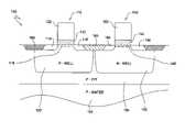
- FIG. 1illustrates portions of a cross sectional view of a field effect transistor (FET) pair in a typical complimentary metal oxide semiconductor (CMOS) device.
- CMOScomplementary metal oxide semiconductor
- Device 100comprises a silicon wafer 155 doped with a p-type material, a p-type epitaxial silicon layer 165 on wafer 155 , a p-type well region 120 and an n-type well region 150 defined in epitaxial layer 165 , an n-type transistor (NMOS FET) 110 defined in p-well 120 and a p-type transistor (PMOS FET) 140 defined in n-well 150 .
- Region 180electrically isolates NMOS 110 and PMOS 140 transistors and region 160 electrically isolates the pair of transistors 110 and 140 from other semiconductor devices on substrate 155 .
- NMOS transistor 110comprises a gate region 122 , a source region 114 and a drain region 116 .
- the source and drain regionsare n-type regions on opposite sides of gate region 122 .
- Channel region 118is interposed between source region 114 and drain region 116 .
- a gate dielectric layer 112separates channel region 118 and gate region 122 .
- Gate dielectric 112electrically insulates gate region 122 from channel region 118 .
- the gate regioncomprises a conductor material, typically doped polycrystalline silicon (polysilicon) or amorphous silicon.
- the dopantmay be an n-type dopant such as a phosphorus or a p-type dopant such as boron.
- PMOS transistor 140comprises a gate region 152 , a source region 144 and a drain region 146 .
- the source and drain regionsare p-type regions on opposite sides of gate region 152 .
- Channel region 148is interposed between source region 144 and drain region 146 .
- a gate dielectric 142separates channel region 148 and gate region 152 .
- Dielectric 142electrically insulates gate region 152 from channel region 148 .
- the gate regioncomprises a conductor material typically doped polysilicon or amorphous silicon. Again, the dopant may be an n-type or p-type material.
- silicon dioxidehas been the material of choice for the gate dielectric layer. Silicon dioxide offers a stable high-quality Si—SiO 2 interface and superior electrical isolation properties.
- the primary issueis that as thickness decreases, leakage current increases. This leakage in current is due primarily to the ability of the electrons to go through the thinner SiO 2 dielectric layer.
- current density for a 1.5 nanometer thick SiO 2 layer at 1 Vis 1 A/cm 2 ; however, as the SiO 2 thickness decreases to 1 nanometer, the leakage-current density approaches 100 A/cm 2 at the same operating voltage.
- the alternative gate dielectric materialmust have a dielectric constant that is higher than that of silicon dioxide.
- the thickness of such an alternative dielectric material layeris expressed in terms of the equivalent oxide thickness (EOT).
- EOTequivalent oxide thickness
- Another consideration in selecting an alternative dielectric materialis the mobility of charge carries in the transistor channel.
- the material selected for the dielectric filmaffects the mobility of the carriers in the transistor channel, thereby affecting overall transistor performance. It is desirable to find an alternative dielectric material for which the mobility of carriers in the transistor channel is equivalent to or higher than that for silicon dioxide gate dielectric films. For future generation transistors, a peak mobility of 400 cm 2 /Vs or greater is desirable.
- the present inventioncomprises forming a metal oxide, metal silicate, or combination metal oxide-metal silicate dielectric stack on a semiconductor wafer.
- the methodcomprises pre-treating the semiconductor wafer, e.g., to remove oxide, with hydrofluoric acid to form an HF-last surface and then pre-treating the HF-last surface with ozonated water for a specified time period.
- a dielectric stackis formed on the pre-treated surface using a chemical vapor deposition process.
- a flow of NH 3is then provided in a process zone surrounding the semiconductor wafer.
- a polycrystalline or amorphous silicon gateis formed over the dielectric stack using a LPCVD process.
- the method of forming a dielectric stack on a semiconductor wafercomprises pre-treating the semiconductor wafer with hydrofluoric acid to form an HF-last surface, pre-treating the HF-last surface with NH 3 , forming the dielectric stack on the pre-treated surface, and providing a flow of N 2 in a process zone surrounding the semiconductor wafer after forming the dielectric stack.
- the method of forming a dielectric stack on a semiconductor wafercomprises pre-treating the semiconductor wafer with hydrofluoric acid to form an HF-last surface, pre-treating the HF-last surface using an in-situ steam generation process, forming the dielectric stack on the pre-treated surface, and annealing the semiconductor wafer after forming the dielectric stack.
- the in-situ steam generation processcomprises providing an inert gas flow in a process zone surrounding the HF-last surface, reacting hydrogen with an oxidizer in the process zone surrounding the HF-last surface for a very short duration, and providing an inert gas flow in the process zone after the reacting step.
- the dielectric stackcomprises layers of hafnium oxide, hafnium silicate layers, or a combination thereof formed using a MOCVD process.
- FIG. 1illustrates portions of a cross sectional view of field effect transistor (FET) pair in a typical complimentary metal oxide semiconductor (CMOS) device.
- FETfield effect transistor
- CMOScomplimentary metal oxide semiconductor
- FIG. 2illustrates a cross-sectional view of a portion of a transistor having a dielectric stack.
- FIG. 3illustrates the processing steps used to form a hafnium oxide and hafnium silicate gate dielectric stack.
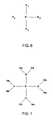
- FIG. 4illustrates the general chemical structure for the hafnium oxide precursors of the form Hf(NRR′) 4 .
- FIG. 5illustrates the chemical structure of the TDEAH precursor.
- FIG. 6illustrates the general chemical structure for precursors of the form SiR 1 R 2 R 3 R 4 .
- FIG. 7illustrates the chemical structure of the TDMAS precursor.
- FIG. 8illustrates the processing steps used to form a hafnium oxide and hafnium silicate gate dielectric stack.
- FIG. 9illustrates the processing steps that may be used for forming the dielectric stack using a flash in-situ steam generation (ISSG) pre-treatment process.
- ISSGflash in-situ steam generation
- FIG. 2illustrates a cross-sectional view of a portion of a field effect (FET) 200 transistor having a dielectric stack in accordance with an embodiment of the invention.
- FET 200comprises a source 250 , a drain 240 , a gate 210 , a dielectric stack 260 and a channel 270 interposed between source 250 and drain 240 .
- the transistoris formed on a silicon wafer and the gate is made of polycrystalline or amorphous silicon.
- source 250 and drain 240comprise a p-type silicon and in an NMOS FET, source 250 and drain 240 comprise an n-type silicon.
- dielectric stack 260comprises at least two layers, where each layer comprises either a metal oxide layer or a metal silicate layer.
- the stackis formed using any metal that is capable of forming a high-k layer, e.g., HfO 2 , ZrO 2 .
- a high-k layercomprises a dielectric material having a dielectric constant greater than 4.
- metal oxide layer 230 and metal silicate layer 220comprise any metal that can form amino precursors. More preferably, metal oxide layer 230 comprises hafnium oxide and the metal silicate layer 220 comprises hafnium silicate.
- the hafnium oxide layer thicknessis about 3 nanometers and the hafnium silicate layer thickness is about 1 nanometer.
- Such a dielectric stackhas an EOT of about 1.12 nanometers.
- the hafnium oxide layer thicknessis about 4 nanometers and hafnium silicate layer thickness is about 1.5 nanometers.
- Such a dielectric stackhas an EOT of about 1.61 nanometers.
- An EOT of 1.61 nanometersprovides the desired peak mobility of 400 cm 2 /Vs.
- the dielectric stack thicknessis selected to provide both the desired capacitance corresponding to 1.12 nanometers EOT and the desired peak mobility of 400 cm 2 /Vs.
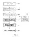
- FIG. 3illustrates the processing steps used in accordance with the invention to form a hafnium oxide, hafnium silicate, or combination thereof gate dielectric stack having an EOT of about 1.12 nanometers.
- an HF-last surfaceis formed on a semiconductor wafer by introducing a dilute hydrofluoric acid solution onto the wafer surface for a specified time period.
- the waferis immersed in a hydrofluoric acid bath for a time period of about 2 minutes to about 15 minutes. More preferably, the wafer is immersed in a 2% hydrofluoric acid bath for about 2 minutes.
- Step 320NH 3 is introduced onto the HF-last surface for a specified time period and at a specified temperature.
- Step 320adds a nitride “coating” or “layer” that aids in preventing the dopant of the gate layer ( 210 in FIG. 2 ) from diffusing into the channel ( 270 in FIG. 2 ).
- the specified time periodis in the range of about 5 seconds to about 120 seconds and the specified temperature is in the range of about 400° C. to about 1,100° C. More preferably, the specified time period is about 30 seconds and the specified temperature is about 600° C. at 30 Torr.
- a hafnium oxide or hafnium silicate layeris then formed at step 330 using deposition processes such as MOCVD, LPCVD, PECVD, VPE, ALD or PVD.
- the hafnium oxide or hafnium silicate layeris formed using a MOCVD process.
- hafnium oxide precursoris any precursor of the alkylamido or alkylamino ligand group.
- the hafnium oxide precursoris selected from a group comprising amino or amido precursors of the form Hf(NRR′) 4 where
- TDEAHis flowed onto the wafer surface at a rate in the range of about 1 mg/min to about 50 mg/min.
- TDEAHis flowed onto the wafer surface at a rate of about 7 mg/min.
- O 2is flowed onto the wafer surface at a rate in the range of about 30 sccm to about 3,000 sccm.
- O 2is flowed onto the wafer surface at a rate of about 1,000 sccm.
- N 2is flowed onto the wafer surface at a rate in the range of about 30 sccm to about 3,000 sccm.
- N 2is flowed onto the wafer surface at a rate of about 1,500 sccm.
- O 2 , N 2 and TDEAHare introduced onto the wafer surface either simultaneously or sequentially or a combination thereof.
- the hafnium oxide layeris formed at temperatures in the range of about 225° C. to about 700° C. Preferably, the hafnium oxide layer is formed at about 485° C.
- the pressure in the deposition chamberis in the range of about 1.5 Torr to about 8 Torr. Preferably, the pressure is about 4 Torr.
- the hafnium oxide layer formedhas a thickness in the range of about 5 ⁇ to about 50 ⁇ . Preferably, the hafnium oxide layer formed has a thickness of about 30 ⁇ .
- the waferis transported to a second chamber after forming the hafnium oxide layer in a first chamber.
- the process conditions of the first chamberare then adjusted for forming the hafnium silicate layer.
- the waferis then transported back to the first chamber for forming the second layer.
- the wafercan remain in the same chamber for sequential deposition of the second layer.
- the choice of whether to use single- or multiple-chamber depositiondepends on a number of factors including the deposition process chosen for each layer (e.g., MOCVD for one layer and ALD for another or MOCVD for both layers), the capabilities or limitations of the system (transfer speed between chambers, temperature ramping capabilities), whether the wafers are being processed in a development or production environment, and/or whether an anneal process is performed between the deposition of the two dielectric layers.
- the hafnium silicate layermay be formed at step 330 using deposition processes such as MOCVD, LPCVD, PECVD, VPE, ALD or PVD.
- the hafnium silicate layeris formed using a MOCVD process, where O 2 , N 2 , and hafnium silicate precursors are introduced onto the wafer surface and the process temperature is about 480° C. to about 600° C. and the pressure is adjusted to about 4 Torr.
- hafnium silicate precursorsare precursors of the alkylamido or alkylamino ligand group.
- the hafnium silicate precursorsare selected from precursors of the form Hf(NRR′) 4 and SiR 1 R 2 R 3 R 4 where
- RH, CH 3 , C 2 H 5 , C 3 H 7 , alkyl, and aryl;
- R′H, CH 3 , C 2 H 5 , C 3 H 7 , alkyl, and aryl;
- R 1H, NH 2 , N(CH 3 ) 2 , N(C 2 H 5 ) 2 , N(C 3 H 7 ) 2 , NCO, alkoxy, amino, alkyl and aryl;
- R 2H, NH 2 , N(CH 3 ) 2 , N(C 2 H 5 ) 2 , N(C 3 H 7 ) 2 , NCO, alkoxy, amino, alkyl and aryl;
- R 3H, NH 2 , N(CH 3 ) 2 , N(C 2 H 5 ) 2 , N(C 3 H 7 ) 2 , NCO, alkoxy, amino, alkyl and aryl;
- R 4H, NH 2 , N(CH 3 ) 2 , N(C 2 H 5 ) 2 , N(C 3 H 7 ) 2 , NCO, alkoxy, amino, alkyl and aryl.
- FIG. 4The general chemical structure for the precursors of the form Hf(NRR′) 4 is shown in FIG. 4 .
- FIG. 6illustrates the general chemical structure for precursors of the form SiR 1 R 2 R 3 R 4 .
- the hafnium silicate precursorsare tetrakis(diethylamido)hafnium (TDEAH) and tetrakis(dimethylamido)silicon (TDMAS).
- TDEAHtetrakis(diethylamido)hafnium
- TDMAStetrakis(dimethylamido)silicon
- FIG. 7illustrates the chemical structure of the TDMAS precursor.
- the chemical structure for the TDEAH precursoris shown in FIG. 5 .
- TDEAHis flowed onto the wafer surface at a rate in the range of about 1 mg/min to about 50 mg/min.
- TDEAHis flowed onto the wafer surface at a rate of about 6 mg/min.
- TDMASis flowed onto the wafer surface at a rate of about 1 mg/min to about 50 mg/min.
- TDMASis flowed at a rate of 50 mg/min.
- O 2is flowed onto the wafer surface at a rate of about 30 sccm to about 1,000 sccm, preferably about 1,000 sccm
- N 2is flowed onto the wafer surface at a rate of about 30 sccm to about 3,000 sccm, preferably about 1,500 sccm.
- O 2 , N 2 , TDEAH and TDMASare introduced onto the wafer surface either simultaneously or sequentially or a combination thereof.
- the hafnium silicate layeris formed at temperatures in the range of about 325° C. to about 700° C. and pressure is in the range of about 1.5 Torr to about 8 Torr. Preferably, the hafnium silicate layer is formed at about 600° C. at a pressure of about 4 Torr.
- the hafnium silicate layer thicknessis about 5-20 ⁇ , preferably 10 ⁇ .
- the SiO 2 concentration of the hafnium silicate layeris from about 5 mol % to about 80 mol %. More preferably, the SiO 2 concentration is about 10 mol %.
- hafnium oxide or hafnium silicate layercan be formed at steps 330 and 340 .
- hafnium oxidebe used to form both layers, it is preferred that the hafnium oxide layers have differing compositions or stoichiometry, for example, a first layer comprised of HfO 2 and a second layer comprised of Hf 2 O 3 .
- hafnium silicate layershave differing compositions and/or stoichiometry.
- the waferis transported back to the thermal chamber for further processing at 1 to 100 Torr.
- N 2is introduced onto the wafer surface for a specified time period and at a specified temperature.
- the specified time periodis in the range of about 5 seconds to about 60 seconds at temperatures in the range of about 400° C. to about 1,100° C. More preferably, N 2 is introduced onto the wafer surface for about 60 seconds at a temperature of about 800° C. at 10 Torr.
- a gate electrodeis next formed at step 360 on the hafnium oxide or hafnium silicate layer.
- the gate electrode layermay be made of polycrystalline or amorphous silicon and is formed using a chemical vapor deposition process such as MOCVD, LPCVD, PECVD, VPE, ALD or PVD.
- the gate electrodeis formed using an LPCVD process where silane or disilane is flowed onto the wafer at temperatures in the range of about 400° C. to about 900° C.
- the gate electrodeis formed at a temperature of about 570° C.
- a nitride layermay be formed on the hafnium oxide or hafnium silicate layer before formation of the polysilicon gate (i.e., to form a layer between the hafnium silicate layer 220 and the polysilicon gate 210 , see FIG. 2 ). This embodiment is illustrated at step 850 of FIG. 8 .
- a nitride layermay be formed between the channel 270 and the hafnium oxide layer 220 . This embodiment is shown at step 320 of FIG. 3 . The nitride layer prevents dopant diffusion from the gate electrode into the silicon channel.
- the polysilicon gate electrode 210is implanted with dopants such as boron and phosphorus; and the structure is then annealed at ⁇ 1000° C. for activation and distribution of the dopant in the polysilicon layer. It is undesirable for dopant to diffuse from the gate electrode layer 210 into the silicon channel 270 . In small doses, such diffusion can affect threshold voltages, and in larger doses such diffusion can increase leakage currents. Either case drastically affects transistor performance.
- dopantssuch as boron and phosphorus
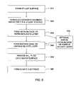
- FIG. 8illustrates the processing steps used in accordance with the invention to form a hafnium oxide and hafnium silicate gate dielectric stack having a peak mobility of about 400 cm 2 /Vs.
- an HF-last surfaceis formed on a semiconductor wafer by introducing a dilute hydrofluoric acid solution onto the wafer surface for a specified time period.
- the waferis immersed in a hydrofluoric acid bath for a time period of about 1 minute to about 15 minutes. More preferably, the wafer is immersed in a 2% hydrofluoric acid bath for about 2 minutes.
- the HF-last surfaceis exposed to ozonated water by, for example, immersing the wafer in an ozonated water bath.
- the ozone concentration in the ozonated wateris in the range of about 10 ppm to about 30 ppm.
- the ozone concentration in the wateris about 20 ppm.
- the HF-last surfaceis exposed to the ozonated water for about 5 minutes to about 15 minutes. More preferably, the HF-last surface is exposed to the ozonated water for about 10 minutes.
- a hafnium oxide layeris then formed at step 830 using deposition processes such as MOCVD, LPCVD, PECVD, VPE, ALD or PVD.
- the hafnium oxide layeris formed using a MOCVD process.
- hafnium oxide precursoris any precursor of the alkylamido or alkylamino ligand group.
- the hafnium oxide precursoris selected from a group comprising amino or amido precursors of the form Hf(NRR′) 4 where
- TDEAHis flowed onto the wafer surface at a rate of about 1 mg/min to about 50 mg/min, preferably about 7 mg/min
- O 2is flowed onto the wafer surface from about 30 sccm to about 3,000 sccm, preferably 30 sccm
- N 2is flowed onto the wafer surface at a rate of about 30 scorn to about 3,000 sccm, preferably about 1500 sccm.
- O 2 , N 2 and TDEAHare introduced onto the wafer surface either simultaneously or sequentially or a combination thereof.
- the hafnium oxide layeris formed at temperatures in the range of about 225° C. to about 700° C., preferably, at about 485° C.
- the pressure in the deposition chamberis in the range of about 3 Torr to about 8 Torr, preferably about 4 Torr.
- the hafnium oxide layer formedhas a thickness of about 2-5 nanometers, and preferably about 4 nanometers.
- the waferis transported from the deposition chamber another chamber.
- the chambermay be an anneal chamber, a cool-down chamber or a loadlock chamber.
- an anneal stepis performed between deposition of the hafnium oxide layer and the hafnium silicate layer.
- the temperature and pressure in the first deposition chamberare adjusted for forming the hafnium silicate layer.
- the temperatureis adjusted to about 600° C. and the pressure is adjusted to about 4 Torr.
- the waferis then transported from the cool-down chamber to the deposition chamber.
- a hafnium silicate layeris then formed at step 840 using deposition processes such as MOCVD, LPCVD, PECVD, VPE, ALD or PVD.
- the waferis not transported to another chamber after forming the hafnium oxide layer, but the wafer remains in the deposition chamber while the process conditions of the deposition chamber are adjusted for forming the hafnium silicate layer.
- ramping the temperature from the processing temperature of the hafnium oxide processing conditions to the temperature of the hafnium silicate processing conditionsprovides an anneal-like environment and a separate anneal step may be eliminated.
- the hafnium silicate layeris formed using a MOCVD process.
- O 2 , N 2 , and hafnium silicate precursorsare introduced onto the wafer surface.
- the hafnium silicate precursorsare precursors of the alkylamido or alkylamino ligand group.
- the hafnium silicate precursorsare selected from precursors of the form Hf(NRR′) 4 and SiR 1 R 2 R 3 R 4 where
- RH, CH 3 , C 2 H 5 , C 3 H 7 , alkyl, and aryl;
- R′H, CH 3 , C 2 H 5 , C 3 H 7 , alkyl, and aryl;
- R 1H, NH 2 , N(CH 3 ) 2 , N(C 2 H 5 ) 2 , N(C 3 H 7 ) 2 , NCO, alkoxy, amino, alkyl and aryl;
- R 2H, NH 2 , N(CH 3 ) 2 , N(C 2 H 5 ) 2 , N(C 3 H 7 ) 2 , NCO, alkoxy, amino, alkyl and aryl;
- R 3H, NH 2 , N(CH 3 ) 2 , N(C 2 H 5 ) 2 , N(C 3 H 7 ) 2 , NCO, alkoxy, amino, alkyl and aryl;
- R 4H, NH 2 , N(CH 3 ) 2 , N(C 2 H 5 ) 2 , N(C 3 H 7 ) 2 , NCO, alkoxy, amino, alkyl and aryl.
- FIG. 4The general chemical structure for the precursors of the form Hf(NRR′) 4 is shown in FIG. 4 .
- FIG. 6illustrates the general chemical structure for precursors of the form SiR 1 R 2 R 3 R 4 .
- the hafnium silicate precursorsare tetrakis(diethylamido)hafnium (TDEAH) and tetrakis(dimethylamido)silicon (TDMAS).
- TDEAHtetrakis(diethylamido)hafnium
- TDMAStetrakis(dimethylamido)silicon
- FIG. 7illustrates the chemical structure of the TDMAS precursor.
- the chemical structure for the TDEAH precursoris shown in FIG. 5 .
- TDEAHis flowed onto the wafer surface at a rate of about 1 mg/min to about 50 mg/min, preferably about 6 mg/min
- TDMASis flowed onto the wafer surface at a rate of about 1 mg/min to about 50 mg/min, preferably about 10 mg/min
- O 2is flowed onto the wafer surface at a rate of about 30 sccm to about 3,000 sccm, preferably about 1,000 sccm
- N 2is flowed onto the wafer surface at a rate of about 30 sccm to about 3,000 sccm, preferably about 1,500 sccm.
- O 2 , N 2 , TDEAH and TDMASare introduced onto the wafer surface either simultaneously or sequentially or a combination thereof.
- the hafnium silicate layeris formed at temperatures in the range of about 325° C. to about 700° C. and at pressure in the range of about 3 Torr to about 8 Torr. Preferably, the hafnium silicate layer is formed at about 600° C. at a pressure of about 4 Torr.
- the hafnium silicate layer thicknessis from 5 to 20 ⁇ , preferably about 1.5 nanometers.
- the SiO 2 concentration of the layeris about 5-80 mol %, preferably about 45 mol % to about 50 mol %. More preferably, the SiO 2 concentration is about 50 mol %.
- the waferis transported from the deposition chamber to the thermal chamber for further processing.
- NH 3is then introduced onto the wafer surface at 1 to 100 Torr for a specified time period and a specified temperature.
- the specified time periodis in the range of about 5 seconds to about 60 seconds. More preferably, the specified time period is about 60 seconds.
- the specified temperatureis in the range of about 400° C. to about 1,100° C. More preferably, the specified temperature is about 700° C. at 30 Torr.
- a polycrystalline-Si or amorphous-Si gate electrodeis next formed at step 860 on the hafnium silicate layer.
- the gate electrode layeris formed using a chemical vapor deposition process such as MOCVD, LPCVD, PECVD, VPE, ALD or PVD.
- the gate electrodeis formed using an LPCVD process where silane or disilane is flowed onto the wafer at temperatures in the range of about 400° C. to about 900° C.
- the gate electrodeis formed at a temperature of about 550° C.
- the wafermay be treated with NH 3 (step 850 of FIG.
- a treatmentforms a nitride coating or layer that prevents dopant diffusion.
- a nitride layermay be formed between the dielectric layer 230 and the silicon channel 270 by treating the wafer with NH 3 ( FIG. 3 , step 330 ) after formation of the HF-last.
- hafnium oxide layerAs described previously, as an alternative to forming first a hafnium oxide layer then forming a hafnium silicate layer, two hafnium oxide layers may be used or two hafnium silicate layers may be used, or first a hafnium silicate layer followed by a hafnium oxide layer may be used.
- a third layermay be formed over the second layer as just described. Such a third layer would comprise hafnium silicate.
- the reactants, hydrogen and an oxidizerare introduced onto an HF-last wafer surface for a very short duration to form hydroxyl groups and water vapor in the thermal chamber
- the hydroxyl groupsthen bond to the HF-last surface, thereby enhancing high-k nucleation.
- the growth of interfacial SiO 2 between the silicon channel and the hafnium oxide layeris minimized due to a very short flash in-situ steam generation process and by introducing inert gases before and after the flash ISSG process.
- FIG. 9illustrates the processing steps that may be used in accordance with the invention for forming the dielectric stack using a flash in-situ steam generation (ISSG) pre-treatment process.
- ISSGflash in-situ steam generation
- an HF-last surfaceis formed on a semiconductor wafer by introducing a dilute hydrofluoric acid solution onto the wafer surface for a specified time period.
- the waferis immersed in a hydrofluoric acid bath for a time period of about 1 minute to about 15 minutes. More preferably, the wafer is immersed in a 2% hydrofluoric acid bath for about 2 minutes.
- the waferis placed in a thermal chamber.
- the HF-last surfaceis then pre-treated using a flash ISSG process.
- an inert gassuch as helium or nitrogen is introduced into the chamber for a specified time period.
- the reactants, hydrogen and an oxidizersuch as O 2 or N 2 O, are introduced into the chamber for a very short duration.
- the flow of reactantsis then stopped at step 940 while the inert gas continues to flow onto the wafer surface at step 950 .
- Table 1provides some illustrative temperatures, flow rates and reactant flow times for a flash ISSG process.
- Example 1750 8 2,980 (O 2 ) 2,980 6
- Example 2750 15 2,980 (N 2 O) 2,980 6
- Example 3750 15 2,980 (O 2 ) 2,980 6
- Example 4800 5 1,000 (O 2 ) 0 3
- Example 5800 5 1,000 (N 2 O) 0 3
- the waferis transported to a deposition chamber.
- a metal oxide and a metal silicate layerare then formed on the pre-treated surface.
- any metal that forms amino precursorsincluding alkoxides or halides, may be used to form the metal oxide and metal silicate layers.
- hafnium oxide and hafnium silicate layersare formed at steps 960 and 970 using the processes described earlier in reference to FIGS. 3 and 8 . Table 2 provides illustrative parameters for forming the hafnium oxide and hafnium silicate layers.
- the waferis transported from the deposition chamber to the thermal chamber for post-deposition processing.
- the post-deposition processingcomprises the post-treatment processes described earlier in reference to FIGS. 3 and 8 .
- the post-deposition processingcomprises annealing the wafer surface at step 980 in a thermal or plasma environment using H 2 , O 2 , N 2 O, NO, NH 3 , O 3 , N 2 , He or a combination thereof.
- a polycrystalline-Si or amorphous-Si gate electrodeis next formed at step 990 after post-deposition processing.
- the gate electrode layeris formed using a deposition process such as MOCVD, LPCVD, PECVD, VPE, ALD or PVD.
- the gate electrodeis formed using an LPCVD process where silane or disilane is flowed onto the wafer at temperatures in the range of about 400° C. to about 900° C.
- the gate electrodeis formed at a temperature of about 550° C.
- a nitride layermay be formed between the dielectric layer 220 and the polysilicon gate 210 prior to formation of the polysilicon gate. Alternately, a nitride layer may be formed between the dielectric layer 230 and the silicon channel 260 .
Landscapes
- Chemical & Material Sciences (AREA)
- Engineering & Computer Science (AREA)
- Chemical Kinetics & Catalysis (AREA)
- Organic Chemistry (AREA)
- Metallurgy (AREA)
- Mechanical Engineering (AREA)
- Materials Engineering (AREA)
- General Chemical & Material Sciences (AREA)
- Physics & Mathematics (AREA)
- Computer Hardware Design (AREA)
- Power Engineering (AREA)
- Microelectronics & Electronic Packaging (AREA)
- Manufacturing & Machinery (AREA)
- General Physics & Mathematics (AREA)
- Condensed Matter Physics & Semiconductors (AREA)
- Thermal Sciences (AREA)
- Crystallography & Structural Chemistry (AREA)
- Inorganic Chemistry (AREA)
- Insulated Gate Type Field-Effect Transistor (AREA)
- Formation Of Insulating Films (AREA)
Abstract
Description
This application is a continuation of U.S. patent application Ser. No. 10/256,563, filed Sep. 27, 2002, and issued as U.S. Pat. No. 6,858,547, which claims benefit of U.S. Provisional Patent Application Ser. No. 60/388,928, filed Jun. 14, 2002. Each of the aforementioned related patent applications is herein incorporated by reference.
1. Field of the Invention
The present invention relates generally to forming gate dielectric in field effect transistors, and particularly to forming metal oxide/metal silicate gate dielectric films using chemical vapor deposition.
2. Description of the Related Art
The present invention is especially useful in forming complementary metal oxide semiconductor (CMOS) integrated-circuit devices and will be described in that context. Other applications will also be mentioned. CMOS technology has enabled the microelectronic industry to simultaneously meet several technological requirements to fuel market expansion. This has been accomplished largely by a calculated reduction (scaling) of the dimensions of the field-effect transistor (FET).FIG. 1 illustrates portions of a cross sectional view of a field effect transistor (FET) pair in a typical complimentary metal oxide semiconductor (CMOS) device.Device 100 comprises asilicon wafer 155 doped with a p-type material, a p-typeepitaxial silicon layer 165 onwafer 155, a p-type well region 120 and an n-type well region 150 defined inepitaxial layer 165, an n-type transistor (NMOS FET)110 defined in p-well 120 and a p-type transistor (PMOS FET)140 defined in n-well150.Region 180 electrically isolatesNMOS 110 andPMOS 140 transistors andregion 160 electrically isolates the pair oftransistors substrate 155.
With the rapid shrinking of the transistor feature size, the gate dielectric thickness has also decreased. For several decades, silicon dioxide has been the material of choice for the gate dielectric layer. Silicon dioxide offers a stable high-quality Si—SiO2interface and superior electrical isolation properties.
However, as the dimensions of the transistor continue to decrease, the continued use of silicon dioxide as a dielectric gate material is problematic. The fundamental problem is the need to keep the capacitance of the gate high while the area of the gate is shrinking faster than the thickness of the gate dielectric. The capacitance C of the gate is given by C=kE0A/d, wherein A is the area of the gate, d is the thickness of the dielectric layer, k is the dielectric constant, and E0is the permittivity of free space. In order to ensure higher gate oxide capacitance, the silicon dioxide layer thickness proportionately has been decreased to less than 2 nanometers as the area of the gate has been decreasing. However, future generations will likely require a further reduction to below 1.0 nanometer. The primary issue is that as thickness decreases, leakage current increases. This leakage in current is due primarily to the ability of the electrons to go through the thinner SiO2dielectric layer. In an example, current density for a 1.5 nanometer thick SiO2layer at 1 V is 1 A/cm2; however, as the SiO2thickness decreases to 1 nanometer, the leakage-current density approaches 100 A/cm2at the same operating voltage.
Consequently, there is a need for an alternative gate dielectric material that can be used in a large enough physical thickness to reduce current leakage density and still provide a high gate capacitance. In order to achieve this, the alternative gate dielectric material must have a dielectric constant that is higher than that of silicon dioxide. Typically, the thickness of such an alternative dielectric material layer is expressed in terms of the equivalent oxide thickness (EOT). Thus, the equivalent oxide thickness (EOT) of an alternative dielectric layer in a particular capacitor is the thickness that the alternative dielectric layer would have if its dielectric constant were that of silicon dioxide.
Another consideration in selecting an alternative dielectric material is the mobility of charge carries in the transistor channel. The material selected for the dielectric film affects the mobility of the carriers in the transistor channel, thereby affecting overall transistor performance. It is desirable to find an alternative dielectric material for which the mobility of carriers in the transistor channel is equivalent to or higher than that for silicon dioxide gate dielectric films. For future generation transistors, a peak mobility of 400 cm2/Vs or greater is desirable.
The present invention comprises forming a metal oxide, metal silicate, or combination metal oxide-metal silicate dielectric stack on a semiconductor wafer.
In one embodiment, the method comprises pre-treating the semiconductor wafer, e.g., to remove oxide, with hydrofluoric acid to form an HF-last surface and then pre-treating the HF-last surface with ozonated water for a specified time period. After pre-treating, a dielectric stack is formed on the pre-treated surface using a chemical vapor deposition process. A flow of NH3is then provided in a process zone surrounding the semiconductor wafer. In one embodiment, after providing the NH3flow, a polycrystalline or amorphous silicon gate is formed over the dielectric stack using a LPCVD process.
In another embodiment, the method of forming a dielectric stack on a semiconductor wafer comprises pre-treating the semiconductor wafer with hydrofluoric acid to form an HF-last surface, pre-treating the HF-last surface with NH3, forming the dielectric stack on the pre-treated surface, and providing a flow of N2in a process zone surrounding the semiconductor wafer after forming the dielectric stack.
In yet another embodiment, the method of forming a dielectric stack on a semiconductor wafer comprises pre-treating the semiconductor wafer with hydrofluoric acid to form an HF-last surface, pre-treating the HF-last surface using an in-situ steam generation process, forming the dielectric stack on the pre-treated surface, and annealing the semiconductor wafer after forming the dielectric stack. The in-situ steam generation process comprises providing an inert gas flow in a process zone surrounding the HF-last surface, reacting hydrogen with an oxidizer in the process zone surrounding the HF-last surface for a very short duration, and providing an inert gas flow in the process zone after the reacting step. Preferably, the dielectric stack comprises layers of hafnium oxide, hafnium silicate layers, or a combination thereof formed using a MOCVD process.
So that the manner in which the above recited features of the present invention, and other features contemplated and claimed herein, are attained and can be understood in detail, a more particular description of the invention, briefly summarized above, may be had by reference to the embodiments which are illustrated in the appended drawings. It is to be noted, however, that the appended drawings illustrate only typical embodiments of this invention and are therefore not to be considered limiting of its scope, for the invention may admit to other equally effective embodiments.
Additional objects and features of the invention will be more readily apparent from the following detailed description and appended claims when taken in conjunction with the drawings, in which:
In one embodiment,dielectric stack 260 comprises at least two layers, where each layer comprises either a metal oxide layer or a metal silicate layer. In the embodiment shown, there is ametal oxide layer 230 and ametal silicate layer 220. The stack is formed using any metal that is capable of forming a high-k layer, e.g., HfO2, ZrO2. A high-k layer comprises a dielectric material having a dielectric constant greater than 4. Preferably,metal oxide layer 230 andmetal silicate layer 220 comprise any metal that can form amino precursors. More preferably,metal oxide layer 230 comprises hafnium oxide and themetal silicate layer 220 comprises hafnium silicate. In one embodiment, the hafnium oxide layer thickness is about 3 nanometers and the hafnium silicate layer thickness is about 1 nanometer. Such a dielectric stack has an EOT of about 1.12 nanometers. In another embodiment, the hafnium oxide layer thickness is about 4 nanometers and hafnium silicate layer thickness is about 1.5 nanometers. Such a dielectric stack has an EOT of about 1.61 nanometers. An EOT of 1.61 nanometers provides the desired peak mobility of 400 cm2/Vs. In yet another embodiment, the dielectric stack thickness is selected to provide both the desired capacitance corresponding to 1.12 nanometers EOT and the desired peak mobility of 400 cm2/Vs.
Next, the wafer is placed in a thermal chamber for pre-treating at 1 to 100 Torr. Astep 320, NH3is introduced onto the HF-last surface for a specified time period and at a specified temperature. Step320 adds a nitride “coating” or “layer” that aids in preventing the dopant of the gate layer (210 inFIG. 2 ) from diffusing into the channel (270 inFIG. 2 ). Preferably, the specified time period is in the range of about 5 seconds to about 120 seconds and the specified temperature is in the range of about 400° C. to about 1,100° C. More preferably, the specified time period is about 30 seconds and the specified temperature is about 600° C. at 30 Torr.
The wafer is then transported from the thermal chamber to a deposition chamber. A hafnium oxide or hafnium silicate layer is then formed atstep 330 using deposition processes such as MOCVD, LPCVD, PECVD, VPE, ALD or PVD. Preferably, the hafnium oxide or hafnium silicate layer is formed using a MOCVD process.
If a hafnium oxide layer is preferred, O2, N2and a hafnium oxide precursor are introduced onto the wafer surface. The hafnium oxide precursor is any precursor of the alkylamido or alkylamino ligand group. In one embodiment, the hafnium oxide precursor is selected from a group comprising amino or amido precursors of the form Hf(NRR′)4where
- R=H, CH3, C2H5, C3H7, alkyl, and aryl and
- R′=H, CH3, C2H5, C3H7, alkyl, and aryl.
FIG. 4 illustrates the general chemical structure for the hafnium oxide precursors of the form Hf(NRR′)4. Preferably, the hafnium oxide precursor is tetrakis(diethylamido)hafnium (TDEAH).FIG. 5 illustrates the chemical structure of the TDEAH precursor.
TDEAH is flowed onto the wafer surface at a rate in the range of about 1 mg/min to about 50 mg/min. Preferably, TDEAH is flowed onto the wafer surface at a rate of about 7 mg/min. O2is flowed onto the wafer surface at a rate in the range of about 30 sccm to about 3,000 sccm. Preferably, O2is flowed onto the wafer surface at a rate of about 1,000 sccm. N2is flowed onto the wafer surface at a rate in the range of about 30 sccm to about 3,000 sccm. Preferably, N2is flowed onto the wafer surface at a rate of about 1,500 sccm. O2, N2and TDEAH are introduced onto the wafer surface either simultaneously or sequentially or a combination thereof.
The hafnium oxide layer is formed at temperatures in the range of about 225° C. to about 700° C. Preferably, the hafnium oxide layer is formed at about 485° C. The pressure in the deposition chamber is in the range of about 1.5 Torr to about 8 Torr. Preferably, the pressure is about 4 Torr. The hafnium oxide layer formed has a thickness in the range of about 5 Å to about 50 Å. Preferably, the hafnium oxide layer formed has a thickness of about 30 Å.
In one embodiment, the wafer is transported to a second chamber after forming the hafnium oxide layer in a first chamber. The process conditions of the first chamber are then adjusted for forming the hafnium silicate layer. The wafer is then transported back to the first chamber for forming the second layer. Alternatively, the wafer can remain in the same chamber for sequential deposition of the second layer. The choice of whether to use single- or multiple-chamber deposition depends on a number of factors including the deposition process chosen for each layer (e.g., MOCVD for one layer and ALD for another or MOCVD for both layers), the capabilities or limitations of the system (transfer speed between chambers, temperature ramping capabilities), whether the wafers are being processed in a development or production environment, and/or whether an anneal process is performed between the deposition of the two dielectric layers.
Alternatively, the hafnium silicate layer may be formed atstep 330 using deposition processes such as MOCVD, LPCVD, PECVD, VPE, ALD or PVD. Preferably, the hafnium silicate layer is formed using a MOCVD process, where O2, N2, and hafnium silicate precursors are introduced onto the wafer surface and the process temperature is about 480° C. to about 600° C. and the pressure is adjusted to about 4 Torr.
The hafnium silicate precursors are precursors of the alkylamido or alkylamino ligand group. The hafnium silicate precursors are selected from precursors of the form Hf(NRR′)4and SiR1R2R3R4where
R=H, CH3, C2H5, C3H7, alkyl, and aryl;
R′=H, CH3, C2H5, C3H7, alkyl, and aryl;
R1=H, NH2, N(CH3)2, N(C2H5)2, N(C3H7)2, NCO, alkoxy, amino, alkyl and aryl;
R2=H, NH2, N(CH3)2, N(C2H5)2, N(C3H7)2, NCO, alkoxy, amino, alkyl and aryl;
R3=H, NH2, N(CH3)2, N(C2H5)2, N(C3H7)2, NCO, alkoxy, amino, alkyl and aryl; and
R4=H, NH2, N(CH3)2, N(C2H5)2, N(C3H7)2, NCO, alkoxy, amino, alkyl and aryl.
The general chemical structure for the precursors of the form Hf(NRR′)4is shown inFIG. 4 .FIG. 6 illustrates the general chemical structure for precursors of the form SiR1R2R3R4. Preferably, the hafnium silicate precursors are tetrakis(diethylamido)hafnium (TDEAH) and tetrakis(dimethylamido)silicon (TDMAS).FIG. 7 illustrates the chemical structure of the TDMAS precursor. The chemical structure for the TDEAH precursor is shown inFIG. 5 .
TDEAH is flowed onto the wafer surface at a rate in the range of about 1 mg/min to about 50 mg/min. Preferably, TDEAH is flowed onto the wafer surface at a rate of about 6 mg/min. TDMAS is flowed onto the wafer surface at a rate of about 1 mg/min to about 50 mg/min. Preferably, TDMAS is flowed at a rate of 50 mg/min. O2is flowed onto the wafer surface at a rate of about 30 sccm to about 1,000 sccm, preferably about 1,000 sccm, and N2is flowed onto the wafer surface at a rate of about 30 sccm to about 3,000 sccm, preferably about 1,500 sccm. O2, N2, TDEAH and TDMAS are introduced onto the wafer surface either simultaneously or sequentially or a combination thereof.
The hafnium silicate layer is formed at temperatures in the range of about 325° C. to about 700° C. and pressure is in the range of about 1.5 Torr to about 8 Torr. Preferably, the hafnium silicate layer is formed at about 600° C. at a pressure of about 4 Torr. The hafnium silicate layer thickness is about 5-20 Å, preferably 10 Å. The SiO2concentration of the hafnium silicate layer is from about 5 mol % to about 80 mol %. More preferably, the SiO2concentration is about 10 mol %.
Thus, either a hafnium oxide or hafnium silicate layer can be formed atsteps
After forming the hafnium silicate layer or hafnium oxide layer atstep 340, the wafer is transported back to the thermal chamber for further processing at 1 to 100 Torr. Atstep 350, N2is introduced onto the wafer surface for a specified time period and at a specified temperature. Preferably, the specified time period is in the range of about 5 seconds to about 60 seconds at temperatures in the range of about 400° C. to about 1,100° C. More preferably, N2is introduced onto the wafer surface for about 60 seconds at a temperature of about 800° C. at 10 Torr.
In one embodiment, a gate electrode is next formed atstep 360 on the hafnium oxide or hafnium silicate layer. The gate electrode layer may be made of polycrystalline or amorphous silicon and is formed using a chemical vapor deposition process such as MOCVD, LPCVD, PECVD, VPE, ALD or PVD. In one embodiment, the gate electrode is formed using an LPCVD process where silane or disilane is flowed onto the wafer at temperatures in the range of about 400° C. to about 900° C. Preferably, the gate electrode is formed at a temperature of about 570° C.
In some embodiments, a nitride layer may be formed on the hafnium oxide or hafnium silicate layer before formation of the polysilicon gate (i.e., to form a layer between thehafnium silicate layer 220 and thepolysilicon gate 210, seeFIG. 2 ). This embodiment is illustrated atstep 850 ofFIG. 8 . Alternatively, for example, a nitride layer may be formed between thechannel 270 and thehafnium oxide layer 220. This embodiment is shown atstep 320 ofFIG. 3 . The nitride layer prevents dopant diffusion from the gate electrode into the silicon channel. In such embodiments, thepolysilicon gate electrode 210 is implanted with dopants such as boron and phosphorus; and the structure is then annealed at ˜1000° C. for activation and distribution of the dopant in the polysilicon layer. It is undesirable for dopant to diffuse from thegate electrode layer 210 into thesilicon channel 270. In small doses, such diffusion can affect threshold voltages, and in larger doses such diffusion can increase leakage currents. Either case drastically affects transistor performance.
Next, atstep 820, the HF-last surface is exposed to ozonated water by, for example, immersing the wafer in an ozonated water bath. Preferably, the ozone concentration in the ozonated water is in the range of about 10 ppm to about 30 ppm. Preferably, the ozone concentration in the water is about 20 ppm. Preferably, the HF-last surface is exposed to the ozonated water for about 5 minutes to about 15 minutes. More preferably, the HF-last surface is exposed to the ozonated water for about 10 minutes.
The wafer is next placed in a deposition chamber. A hafnium oxide layer is then formed atstep 830 using deposition processes such as MOCVD, LPCVD, PECVD, VPE, ALD or PVD. Preferably, the hafnium oxide layer is formed using a MOCVD process.
O2, N2and a hafnium oxide precursor are introduced onto the wafer surface. The hafnium oxide precursor is any precursor of the alkylamido or alkylamino ligand group. In one embodiment, the hafnium oxide precursor is selected from a group comprising amino or amido precursors of the form Hf(NRR′)4where
- R=H, CH3, C2H5, C3H7, alkyl, and aryl and
- R′=H, CH3, C2H5, C3H7, alkyl, and aryl.
FIG. 4 illustrates the general chemical structure for the hafnium oxide precursors of the form Hf(NRR′)4. Preferably, the hafnium oxide precursor is tetrakis(diethylamido)hafnium (TDEAH).FIG. 5 illustrates the chemical structure of the TDEAH precursor.
TDEAH is flowed onto the wafer surface at a rate of about 1 mg/min to about 50 mg/min, preferably about 7 mg/min, O2is flowed onto the wafer surface from about 30 sccm to about 3,000 sccm, preferably 30 sccm, and N2is flowed onto the wafer surface at a rate of about 30 scorn to about 3,000 sccm, preferably about 1500 sccm. O2, N2and TDEAH are introduced onto the wafer surface either simultaneously or sequentially or a combination thereof.
The hafnium oxide layer is formed at temperatures in the range of about 225° C. to about 700° C., preferably, at about 485° C. The pressure in the deposition chamber is in the range of about 3 Torr to about 8 Torr, preferably about 4 Torr. Preferably, the hafnium oxide layer formed has a thickness of about 2-5 nanometers, and preferably about 4 nanometers.
After forming the hafnium oxide layer, the wafer is transported from the deposition chamber another chamber. For example, the chamber may be an anneal chamber, a cool-down chamber or a loadlock chamber. Preferably, an anneal step is performed between deposition of the hafnium oxide layer and the hafnium silicate layer. Once the wafer is transferred, the temperature and pressure in the first deposition chamber are adjusted for forming the hafnium silicate layer. For an MOCVD process, the temperature is adjusted to about 600° C. and the pressure is adjusted to about 4 Torr. The wafer is then transported from the cool-down chamber to the deposition chamber. A hafnium silicate layer is then formed atstep 840 using deposition processes such as MOCVD, LPCVD, PECVD, VPE, ALD or PVD. In another embodiment, the wafer is not transported to another chamber after forming the hafnium oxide layer, but the wafer remains in the deposition chamber while the process conditions of the deposition chamber are adjusted for forming the hafnium silicate layer. In this case, ramping the temperature from the processing temperature of the hafnium oxide processing conditions to the temperature of the hafnium silicate processing conditions provides an anneal-like environment and a separate anneal step may be eliminated.
Preferably, the hafnium silicate layer is formed using a MOCVD process. O2, N2, and hafnium silicate precursors are introduced onto the wafer surface. The hafnium silicate precursors are precursors of the alkylamido or alkylamino ligand group. The hafnium silicate precursors are selected from precursors of the form Hf(NRR′)4and SiR1R2R3R4where
R=H, CH3, C2H5, C3H7, alkyl, and aryl;
R′=H, CH3, C2H5, C3H7, alkyl, and aryl;
R1=H, NH2, N(CH3)2, N(C2H5)2, N(C3H7)2, NCO, alkoxy, amino, alkyl and aryl;
R2=H, NH2, N(CH3)2, N(C2H5)2, N(C3H7)2, NCO, alkoxy, amino, alkyl and aryl;
R3=H, NH2, N(CH3)2, N(C2H5)2, N(C3H7)2, NCO, alkoxy, amino, alkyl and aryl; and
R4=H, NH2, N(CH3)2, N(C2H5)2, N(C3H7)2, NCO, alkoxy, amino, alkyl and aryl.
The general chemical structure for the precursors of the form Hf(NRR′)4is shown inFIG. 4 .FIG. 6 illustrates the general chemical structure for precursors of the form SiR1R2R3R4. Preferably, the hafnium silicate precursors are tetrakis(diethylamido)hafnium (TDEAH) and tetrakis(dimethylamido)silicon (TDMAS).FIG. 7 illustrates the chemical structure of the TDMAS precursor. The chemical structure for the TDEAH precursor is shown inFIG. 5 .
TDEAH is flowed onto the wafer surface at a rate of about 1 mg/min to about 50 mg/min, preferably about 6 mg/min, TDMAS is flowed onto the wafer surface at a rate of about 1 mg/min to about 50 mg/min, preferably about 10 mg/min, O2is flowed onto the wafer surface at a rate of about 30 sccm to about 3,000 sccm, preferably about 1,000 sccm, and N2is flowed onto the wafer surface at a rate of about 30 sccm to about 3,000 sccm, preferably about 1,500 sccm. O2, N2, TDEAH and TDMAS are introduced onto the wafer surface either simultaneously or sequentially or a combination thereof.
The hafnium silicate layer is formed at temperatures in the range of about 325° C. to about 700° C. and at pressure in the range of about 3 Torr to about 8 Torr. Preferably, the hafnium silicate layer is formed at about 600° C. at a pressure of about 4 Torr. The hafnium silicate layer thickness is from 5 to 20 Å, preferably about 1.5 nanometers. The SiO2concentration of the layer is about 5-80 mol %, preferably about 45 mol % to about 50 mol %. More preferably, the SiO2concentration is about 50 mol %.
After forming the hafnium silicate layer, the wafer is transported from the deposition chamber to the thermal chamber for further processing. Atstep 850 NH3is then introduced onto the wafer surface at 1 to 100 Torr for a specified time period and a specified temperature. Preferably, the specified time period is in the range of about 5 seconds to about 60 seconds. More preferably, the specified time period is about 60 seconds. Preferably, the specified temperature is in the range of about 400° C. to about 1,100° C. More preferably, the specified temperature is about 700° C. at 30 Torr.
In one embodiment, a polycrystalline-Si or amorphous-Si gate electrode is next formed atstep 860 on the hafnium silicate layer. The gate electrode layer is formed using a chemical vapor deposition process such as MOCVD, LPCVD, PECVD, VPE, ALD or PVD. In one embodiment, the gate electrode is formed using an LPCVD process where silane or disilane is flowed onto the wafer at temperatures in the range of about 400° C. to about 900° C. Preferably, the gate electrode is formed at a temperature of about 550° C. As described supra, to avoid undesired dopant diffusion from the gate electrode into the silicon channel, the wafer may be treated with NH3(step850 ofFIG. 8 ) after deposition of thedielectric layer 220 and before deposition of the polysilicon gate210 (layers shown inFIG. 3 ). Such a treatment forms a nitride coating or layer that prevents dopant diffusion. Alternately, a nitride layer may be formed between thedielectric layer 230 and thesilicon channel 270 by treating the wafer with NH3(FIG. 3 , step330) after formation of the HF-last.
As described previously, as an alternative to forming first a hafnium oxide layer then forming a hafnium silicate layer, two hafnium oxide layers may be used or two hafnium silicate layers may be used, or first a hafnium silicate layer followed by a hafnium oxide layer may be used. Optionally, a third layer may be formed over the second layer as just described. Such a third layer would comprise hafnium silicate.
In the flash in-situ steam generation (ISSG) process in accordance with the invention, the reactants, hydrogen and an oxidizer, are introduced onto an HF-last wafer surface for a very short duration to form hydroxyl groups and water vapor in the thermal chamber The hydroxyl groups then bond to the HF-last surface, thereby enhancing high-k nucleation. In accordance with the invention, the growth of interfacial SiO2between the silicon channel and the hafnium oxide layer is minimized due to a very short flash in-situ steam generation process and by introducing inert gases before and after the flash ISSG process.
After the HF-last processing, the wafer is placed in a thermal chamber. The HF-last surface is then pre-treated using a flash ISSG process. First, atstep 920, an inert gas such as helium or nitrogen is introduced into the chamber for a specified time period. Then, atstep 930, the reactants, hydrogen and an oxidizer such as O2or N2O, are introduced into the chamber for a very short duration. The flow of reactants is then stopped atstep 940 while the inert gas continues to flow onto the wafer surface atstep 950. Table 1 provides some illustrative temperatures, flow rates and reactant flow times for a flash ISSG process.
| TABLE 1 | ||||||
| Reactant | ||||||
| Temp. | Oxidizer | Flow | ||||
| (° C.) | H2(sccm) | (sccm) | He (sccm) | Time(s) | ||
| Example 1 | 750 | 8 | 2,980 (O2) | 2,980 | 6 |
| Example 2 | 750 | 15 | 2,980 (N2O) | 2,980 | 6 |
| Example 3 | 750 | 15 | 2,980 (O2) | 2,980 | 6 |
| Example 4 | 800 | 5 | 1,000 (O2) | 0 | 3 |
| Example 5 | 800 | 5 | 1,000 (N2O) | 0 | 3 |
After the pre-treating, the wafer is transported to a deposition chamber. A metal oxide and a metal silicate layer are then formed on the pre-treated surface. Preferably, any metal that forms amino precursors, including alkoxides or halides, may be used to form the metal oxide and metal silicate layers. In one embodiment, hafnium oxide and hafnium silicate layers are formed atsteps FIGS. 3 and 8 . Table 2 provides illustrative parameters for forming the hafnium oxide and hafnium silicate layers.
| TABLE 2 | |||||||
| Pres- | |||||||
| Hf | Si | O2 | N2 | Temp. | sure | ||
| (mg/min) | (mg/min) | (sccm) | (sccm) | (° C.) | (Torr) | ||
| Example 6 | 7 | 0 | 1,000 | 1,500 | 485 | 4 |
| Example 7 | 6 | 50 | 1,750 | 750 | 425 | 3 |
| Example 8 | 6 | 50 | 1,750 | 750 | 525 | 5.5 |
| Example 9 | 6 | 50 | 1,750 | 750 | 575 | 8 |
After forming the metal oxide and metal silicate layers, the wafer is transported from the deposition chamber to the thermal chamber for post-deposition processing. In one embodiment, the post-deposition processing comprises the post-treatment processes described earlier in reference toFIGS. 3 and 8 . In another embodiment, the post-deposition processing comprises annealing the wafer surface atstep 980 in a thermal or plasma environment using H2, O2, N2O, NO, NH3, O3, N2, He or a combination thereof.
In one embodiment, a polycrystalline-Si or amorphous-Si gate electrode is next formed atstep 990 after post-deposition processing. The gate electrode layer is formed using a deposition process such as MOCVD, LPCVD, PECVD, VPE, ALD or PVD. In one embodiment, the gate electrode is formed using an LPCVD process where silane or disilane is flowed onto the wafer at temperatures in the range of about 400° C. to about 900° C. Preferably, the gate electrode is formed at a temperature of about 550° C. To avoid undesired dopant diffusion, a nitride layer may be formed between thedielectric layer 220 and thepolysilicon gate 210 prior to formation of the polysilicon gate. Alternately, a nitride layer may be formed between thedielectric layer 230 and thesilicon channel 260.
Various modifications may occur to those skilled in the art without departing from the true spirit and scope of the invention as defined by the appended claims. For example, although the specific embodiments are described using a hafnium oxide and hafnium silicate dielectric gate stack, those skilled in the art will appreciate that the dielectric stack may be formed using any metal that is capable of forming films with the desired capacitance and mobility. Additionally, although the specific embodiments use metal oxide and metal silicate films, other film compositions that provide the desired capacitance and mobility may also be used to form the dielectric stack.
While the foregoing is directed to embodiments of the present invention, other and further embodiments of the invention may be devised without departing from the basic scope thereof, and the scope thereof is determined by the claims that follow.
Claims (29)
1. A method for forming a dielectric stack material on a substrate, comprising:
treating the substrate with hydrofluoric acid to form an HF-last surface;
pre-treating the HF-last surface with an oxidation process for a specified time period to form a pre-treated surface, wherein the oxidation process comprises exposing the substrate to in situ steam generated from hydrogen gas (H2) and oxygen gas (O2) or from hydrogen gas and nitrous oxide;
forming a dielectric stack on the pre-treated surface, wherein the dielectric stack comprises at least one material selected from the group consisting of hafnium oxide, hafnium silicate, and combinations thereof; and
exposing the substrate to a nitridation process to form a nitride layer on the dielectric stack.
2. The method ofclaim 1 , wherein the dielectric stack comprises a hafnium silicate layer deposited on a hafnium oxide layer.
3. The method ofclaim 2 , wherein the hafnium oxide layer and the hafnium silicate layer are each formed using a deposition process independently selected from the group consisting of chemical vapor deposition, atomic layer deposition, and combinations thereof.
4. The method ofclaim 3 , wherein the deposition process comprises exposing the substrate to a hafnium precursor having the chemical formula (RR′N)4Hf, wherein R and R′ are independently selected from the group consisting of hydrogen, methyl, ethyl, propyl, and combinations thereof.
5. The method ofclaim 4 , wherein the deposition process comprises exposing the substrate to a silicon precursor having the chemical formula R1R2R3R4Si, wherein R1, R2, R3, and R4are independently selected from the group consisting of hydrogen, alkyl, alkoxy, amino, dimethylamino, diethylamino, dipropylamino, and combinations thereof.
6. The method ofclaim 5 , wherein the substrate is exposed to an annealing process subsequent the formation of the dielectric stack.
7. A method for forming a dielectric stack material on a substrate, comprising:
pre-treating the substrate with an oxidation process for a specified time period to form a pre-treated surface, wherein the oxidation process comprises exposing the substrate to in situ steam generated from hydrogen gas (H2) and oxygen gas (O2) or from hydrogen gas and nitrous oxide;
forming a hafnium oxide layer on the pre-treated surface;
forming a hafnium silicate layer on the hafnium oxide layer to form a dielectric stack; and
exposing the substrate to a nitridation process to form a nitride layer on the dielectric stack.
8. The method ofclaim 7 , wherein the hafnium oxide layer and the hafnium silicate layer are each formed using a deposition process independently selected from the group consisting of chemical vapor deposition, atomic layer deposition, and combinations thereof.
9. The method ofclaim 8 , wherein the deposition process comprises exposing the substrate to a hafnium precursor having the chemical formula (RR′N)4Hf, wherein R and R′ are independently selected from the group consisting of hydrogen, methyl, ethyl, propyl, and combinations thereof.
10. The method ofclaim 9 , wherein the deposition process comprises exposing the substrate to a silicon precursor having the chemical formula R1R2R3R4Si, wherein R1, R2, R3, and R4are independently selected from the group consisting of hydrogen, alkyl, alkoxy, amino, dimethylamino, diethylamino, dipropylamino, and combinations thereof.
11. The method ofclaim 10 , wherein the substrate is exposed to an annealing process subsequent the formation of the dielectric stack.
12. The method ofclaim 11 , wherein the substrate comprises a HF-last surface prior to forming the pre-treated surface.
13. A method for forming a dielectric stack material on a substrate, comprising:
treating the substrate with hydrofluoric acid to form an HF-last surface;
pre-treating the HF-last surface to form a pre-treated surface with a pre-treatment process selected from the group consisting of an oxidation process and a combination of a first nitridation process and an oxidation process, wherein the oxidation process comprises exposing the substrate to in situ steam generated from hydrogen gas (H2) and oxygen gas (O2) or from hydrogen gas and nitrous oxide;
forming a dielectric stack on the pre-treated surface, wherein the dielectric stack comprises hafnium silicate and hafnium oxide;
exposing the substrate to a second nitridation process to form a nitride layer on the dielectric stack; and
forming a polycrystalline-Si layer or an amorphous-Si layer over the dielectric stack.
14. The method ofclaim 13 , wherein the polycrystalline-Si layer or the amorphous-Si layer is formed by exposing the substrate to silane or disilane during a vapor deposition process at a temperature within a range from about 400° C. to about 900° C.
15. The method ofclaim 13 , wherein the dielectric stack comprises a hafnium silicate layer deposited on a hafnium oxide layer.
16. The method ofclaim 15 , wherein the hafnium oxide layer and the hafnium silicate layer are each formed using a deposition process independently selected from the group consisting of chemical vapor deposition, atomic layer deposition, and combinations thereof.
17. The method ofclaim 16 , wherein the deposition process comprises exposing the substrate to a hafnium precursor having the chemical formula (RR′N)4Hf, wherein R and R′ are independently selected from the group consisting of hydrogen, methyl, ethyl, propyl, and combinations thereof.
18. The method ofclaim 17 , wherein the deposition process comprises exposing the substrate to a silicon precursor having the chemical formula R1R2R3R4Si, wherein R1, R2, R3, and R4are independently selected from the group consisting of hydrogen, alkyl, alkoxy, amino, dimethylamino, diethylamino, dipropylamino, and combinations thereof.
19. The method ofclaim 18 , wherein the substrate is exposed to an annealing process subsequent the formation of the dielectric stack.
20. The method ofclaim 1 , further comprising forming a polycrystalline-Si layer or an amorphous-Si layer over the dielectric stack subsequent to the second nitridation process.
21. The method ofclaim 20 , wherein the polycrystalline-Si layer or the amorphous-Si layer is formed by exposing the substrate to silane or disilane during a vapor deposition process at a temperature within a range from about 400° C. to about 900° C.
22. The method ofclaim 7 , further comprising forming a polycrystalline-Si layer or an amorphous-Si layer over the dielectric stack subsequent to the second nitridation process.
23. The method ofclaim 22 , wherein the polycrystalline-Si layer or the amorphous-Si layer is formed by exposing the substrate to silane or disilane during a vapor deposition process at a temperature within a range from about 400° C. to about 900° C.
24. The method ofclaim 1 , wherein the hafnium oxide layer or the hafnium silicate layer is formed by an atomic layer deposition process which exposes to substrate a hafnium precursor having the chemical formula (RR′N)4Hf, wherein R and R′ are independently methyl or ethyl.
25. The method ofclaim 24 , wherein the hafnium silicate layer is formed by exposing the substrate to a silicon precursor having the chemical formula R1R2R3R4Si, wherein R1, R2, R3, and R4are independently selected from the group consisting of hydrogen, alkyl, alkoxy, amino, dimethylamino, diethylamino, dipropylamino, and combinations thereof.
26. The method ofclaim 7 , wherein the hafnium oxide layer or the hafnium silicate layer is formed by an atomic layer deposition process which exposes to substrate a hafnium precursor having the chemical formula (RR′N)4Hf, wherein R and R′ are independently methyl or ethyl.
27. The method ofclaim 26 , wherein the hafnium silicate layer is formed by exposing the substrate to a silicon precursor having the chemical formula R1R2R3R4Si, wherein R1, R2, R3, and R4are independently selected from the group consisting of hydrogen, alkyl, alkoxy, amino, dimethylamino, diethylamino, dipropylamino, and combinations thereof.
28. The method ofclaim 13 , wherein the hafnium oxide layer or the hafnium silicate layer is formed by an atomic layer deposition process which exposes to substrate a hafnium precursor having the chemical formula (RR′N)4Hf, wherein R and R′ are independently methyl or ethyl.
29. The method ofclaim 28 , wherein the hafnium silicate layer is formed by exposing the substrate to a silicon precursor having the chemical formula R1R2R3R4Si, wherein R1, R2, R3, and R4are independently selected from the group consisting of hydrogen, alkyl, alkoxy, amino, dimethylamino, diethylamino, dipropylamino, and combinations thereof.
Priority Applications (2)
| Application Number | Priority Date | Filing Date | Title |
|---|---|---|---|
| US10/913,941US7304004B2 (en) | 2002-06-14 | 2004-08-06 | System and method for forming a gate dielectric |
| US11/929,087US7531468B2 (en) | 2002-06-14 | 2007-10-30 | System and method for forming a gate dielectric |
Applications Claiming Priority (3)
| Application Number | Priority Date | Filing Date | Title |
|---|---|---|---|
| US38892802P | 2002-06-14 | 2002-06-14 | |
| US10/256,563US6858547B2 (en) | 2002-06-14 | 2002-09-27 | System and method for forming a gate dielectric |
| US10/913,941US7304004B2 (en) | 2002-06-14 | 2004-08-06 | System and method for forming a gate dielectric |
Related Parent Applications (1)
| Application Number | Title | Priority Date | Filing Date |
|---|---|---|---|
| US10/256,563ContinuationUS6858547B2 (en) | 2002-06-14 | 2002-09-27 | System and method for forming a gate dielectric |
Related Child Applications (1)
| Application Number | Title | Priority Date | Filing Date |
|---|---|---|---|
| US11/929,087ContinuationUS7531468B2 (en) | 2002-06-14 | 2007-10-30 | System and method for forming a gate dielectric |
Publications (2)
| Publication Number | Publication Date |
|---|---|
| US20050009371A1 US20050009371A1 (en) | 2005-01-13 |
| US7304004B2true US7304004B2 (en) | 2007-12-04 |
Family
ID=29739185
Family Applications (3)
| Application Number | Title | Priority Date | Filing Date |
|---|---|---|---|
| US10/256,563Expired - Fee RelatedUS6858547B2 (en) | 2002-06-14 | 2002-09-27 | System and method for forming a gate dielectric |
| US10/913,941Expired - Fee RelatedUS7304004B2 (en) | 2002-06-14 | 2004-08-06 | System and method for forming a gate dielectric |
| US11/929,087Expired - Fee RelatedUS7531468B2 (en) | 2002-06-14 | 2007-10-30 | System and method for forming a gate dielectric |
Family Applications Before (1)
| Application Number | Title | Priority Date | Filing Date |
|---|---|---|---|
| US10/256,563Expired - Fee RelatedUS6858547B2 (en) | 2002-06-14 | 2002-09-27 | System and method for forming a gate dielectric |
Family Applications After (1)
| Application Number | Title | Priority Date | Filing Date |
|---|---|---|---|
| US11/929,087Expired - Fee RelatedUS7531468B2 (en) | 2002-06-14 | 2007-10-30 | System and method for forming a gate dielectric |
Country Status (1)
| Country | Link |
|---|---|
| US (3) | US6858547B2 (en) |
Cited By (12)
| Publication number | Priority date | Publication date | Assignee | Title |
|---|---|---|---|---|
| US20050253181A1 (en)* | 2004-05-14 | 2005-11-17 | Nec Electronics Corporation | Semiconductor device |
| US20090047798A1 (en)* | 2007-08-16 | 2009-02-19 | Tokyo Electron Limited | Method of forming high dielectric constant films using a plurality of oxidation sources |
| US7531468B2 (en)* | 2002-06-14 | 2009-05-12 | Applied Materials, Inc. | System and method for forming a gate dielectric |
| US20090163012A1 (en)* | 2007-12-21 | 2009-06-25 | Tokyo Electron Limited | Method of forming high-dielectric constant films for semiconductor devices |
| US7569500B2 (en) | 2002-06-14 | 2009-08-04 | Applied Materials, Inc. | ALD metal oxide deposition process using direct oxidation |
| US7645710B2 (en) | 2006-03-09 | 2010-01-12 | Applied Materials, Inc. | Method and apparatus for fabricating a high dielectric constant transistor gate using a low energy plasma system |
| US7678710B2 (en) | 2006-03-09 | 2010-03-16 | Applied Materials, Inc. | Method and apparatus for fabricating a high dielectric constant transistor gate using a low energy plasma system |
| US7837838B2 (en) | 2006-03-09 | 2010-11-23 | Applied Materials, Inc. | Method of fabricating a high dielectric constant transistor gate using a low energy plasma apparatus |
| US7902018B2 (en) | 2006-09-26 | 2011-03-08 | Applied Materials, Inc. | Fluorine plasma treatment of high-k gate stack for defect passivation |
| US8119210B2 (en) | 2004-05-21 | 2012-02-21 | Applied Materials, Inc. | Formation of a silicon oxynitride layer on a high-k dielectric material |
| US8643115B2 (en) | 2011-01-14 | 2014-02-04 | International Business Machines Corporation | Structure and method of Tinv scaling for high κ metal gate technology |
| US11542597B2 (en) | 2020-04-08 | 2023-01-03 | Applied Materials, Inc. | Selective deposition of metal oxide by pulsed chemical vapor deposition |
Families Citing this family (475)
| Publication number | Priority date | Publication date | Assignee | Title |
|---|---|---|---|---|
| US6620723B1 (en) | 2000-06-27 | 2003-09-16 | Applied Materials, Inc. | Formation of boride barrier layers using chemisorption techniques |
| US7588989B2 (en)* | 2001-02-02 | 2009-09-15 | Samsung Electronic Co., Ltd. | Dielectric multilayer structures of microelectronic devices and methods for fabricating the same |
| US6846516B2 (en) | 2002-04-08 | 2005-01-25 | Applied Materials, Inc. | Multiple precursor cyclical deposition system |
| US20030232501A1 (en) | 2002-06-14 | 2003-12-18 | Kher Shreyas S. | Surface pre-treatment for enhancement of nucleation of high dielectric constant materials |
| WO2004008544A1 (en)* | 2002-07-16 | 2004-01-22 | Nec Corporation | Semiconductor device, production method and production device thereof |
| TW200408015A (en)* | 2002-08-18 | 2004-05-16 | Asml Us Inc | Atomic layer deposition of high K metal silicates |
| TW200408323A (en)* | 2002-08-18 | 2004-05-16 | Asml Us Inc | Atomic layer deposition of high k metal oxides |
| KR100460273B1 (en)* | 2003-03-25 | 2004-12-08 | 매그나칩 반도체 유한회사 | Method for manufacturing mos varactor |
| JP4009550B2 (en)* | 2003-03-27 | 2007-11-14 | エルピーダメモリ株式会社 | Method for forming metal oxide film |
| US20040198069A1 (en) | 2003-04-04 | 2004-10-07 | Applied Materials, Inc. | Method for hafnium nitride deposition |
| JP2004311782A (en)* | 2003-04-08 | 2004-11-04 | Tokyo Electron Ltd | Film forming method and film forming apparatus |
| WO2005013374A1 (en)* | 2003-08-05 | 2005-02-10 | Fujitsu Limited | Semiconductor device and method for manufacturing semiconductor device |
| US7258895B2 (en)* | 2003-08-06 | 2007-08-21 | Micron Technology, Inc. | Methods of forming material on a substrate, and a method of forming a field effect transistor gate oxide on a substrate |
| JP2005072405A (en)* | 2003-08-27 | 2005-03-17 | Sony Corp | Thin film forming method and semiconductor device manufacturing method |
| JP2005079223A (en)* | 2003-08-29 | 2005-03-24 | Toshiba Corp | Semiconductor device and manufacturing method of semiconductor device |
| US20050153571A1 (en)* | 2003-11-17 | 2005-07-14 | Yoshihide Senzaki | Nitridation of high-k dielectric films |
| US20060062910A1 (en)* | 2004-03-01 | 2006-03-23 | Meiere Scott H | Low zirconium, hafnium-containing compositions, processes for the preparation thereof and methods of use thereof |
| US7514360B2 (en)* | 2004-03-17 | 2009-04-07 | Hong Yu Yu | Thermal robust semiconductor device using HfN as metal gate electrode and the manufacturing process thereof |
| WO2005098961A1 (en)* | 2004-04-09 | 2005-10-20 | Tokyo Electron Limited | Method of forming gate insulating film, storage medium and computer program |
| US20050252449A1 (en) | 2004-05-12 | 2005-11-17 | Nguyen Son T | Control of gas flow and delivery to suppress the formation of particles in an MOCVD/ALD system |
| US8323754B2 (en) | 2004-05-21 | 2012-12-04 | Applied Materials, Inc. | Stabilization of high-k dielectric materials |
| KR100578819B1 (en)* | 2004-07-15 | 2006-05-11 | 삼성전자주식회사 | Atomic layer deposition method, method of manufacturing gate structure using same and method of manufacturing capacitor |
| KR100593659B1 (en)* | 2004-07-21 | 2006-06-28 | 삼성전자주식회사 | Atomic layer deposition method, method of manufacturing gate structure using same and method of manufacturing capacitor |
| KR100611072B1 (en)* | 2004-08-11 | 2006-08-10 | 삼성전자주식회사 | Atomic layer deposition method, method of manufacturing gate structure using same and method of manufacturing capacitor |
| US20070196011A1 (en)* | 2004-11-22 | 2007-08-23 | Cox Damon K | Integrated vacuum metrology for cluster tool |
| JP2008521261A (en)* | 2004-11-22 | 2008-06-19 | アプライド マテリアルズ インコーポレイテッド | Substrate processing apparatus using batch processing chamber |
| US7235492B2 (en)* | 2005-01-31 | 2007-06-26 | Applied Materials, Inc. | Low temperature etchant for treatment of silicon-containing surfaces |
| KR100584783B1 (en)* | 2005-02-24 | 2006-05-30 | 삼성전자주식회사 | Composite film formation method and gate structure and capacitor manufacturing method using the same |
| US7550055B2 (en)* | 2005-05-31 | 2009-06-23 | Applied Materials, Inc. | Elastomer bonding of large area sputtering target |
| JP2006344837A (en)* | 2005-06-09 | 2006-12-21 | Matsushita Electric Ind Co Ltd | Semiconductor device and manufacturing method thereof |
| US7648927B2 (en) | 2005-06-21 | 2010-01-19 | Applied Materials, Inc. | Method for forming silicon-containing materials during a photoexcitation deposition process |
| US7651955B2 (en) | 2005-06-21 | 2010-01-26 | Applied Materials, Inc. | Method for forming silicon-containing materials during a photoexcitation deposition process |
| US7429538B2 (en)* | 2005-06-27 | 2008-09-30 | Applied Materials, Inc. | Manufacturing method for two-step post nitridation annealing of plasma nitrided gate dielectric |
| US7550381B2 (en)* | 2005-07-18 | 2009-06-23 | Applied Materials, Inc. | Contact clean by remote plasma and repair of silicide surface |
| US20070020890A1 (en)* | 2005-07-19 | 2007-01-25 | Applied Materials, Inc. | Method and apparatus for semiconductor processing |
| US20070037412A1 (en)* | 2005-08-05 | 2007-02-15 | Tokyo Electron Limited | In-situ atomic layer deposition |
| US7402534B2 (en)* | 2005-08-26 | 2008-07-22 | Applied Materials, Inc. | Pretreatment processes within a batch ALD reactor |
| US7387972B2 (en)* | 2006-03-01 | 2008-06-17 | Promos Technologies Pte. Ltd. | Reducing nitrogen concentration with in-situ steam generation |
| US20070252299A1 (en)* | 2006-04-27 | 2007-11-01 | Applied Materials, Inc. | Synchronization of precursor pulsing and wafer rotation |
| US7798096B2 (en) | 2006-05-05 | 2010-09-21 | Applied Materials, Inc. | Plasma, UV and ion/neutral assisted ALD or CVD in a batch tool |
| US20070259111A1 (en)* | 2006-05-05 | 2007-11-08 | Singh Kaushal K | Method and apparatus for photo-excitation of chemicals for atomic layer deposition of dielectric film |
| EP2029790A1 (en)* | 2006-06-02 | 2009-03-04 | L'AIR LIQUIDE, Société Anonyme pour l'Etude et l'Exploitation des Procédés Georges Claude | Method of forming high-k dielectric films based on novel titanium, zirconium, and hafnium precursors and their use for semiconductor manufacturing |
| US8986456B2 (en) | 2006-10-10 | 2015-03-24 | Asm America, Inc. | Precursor delivery system |
| JP5039396B2 (en)* | 2007-02-19 | 2012-10-03 | ローム株式会社 | Manufacturing method of semiconductor device |
| US7910497B2 (en)* | 2007-07-30 | 2011-03-22 | Applied Materials, Inc. | Method of forming dielectric layers on a substrate and apparatus therefor |
| JP2009170439A (en)* | 2008-01-10 | 2009-07-30 | Panasonic Corp | Method for forming gate insulating film |
| US7871942B2 (en)* | 2008-03-27 | 2011-01-18 | Applied Materials, Inc. | Methods for manufacturing high dielectric constant film |
| US7816278B2 (en)* | 2008-03-28 | 2010-10-19 | Tokyo Electron Limited | In-situ hybrid deposition of high dielectric constant films using atomic layer deposition and chemical vapor deposition |
| US7659158B2 (en) | 2008-03-31 | 2010-02-09 | Applied Materials, Inc. | Atomic layer deposition processes for non-volatile memory devices |
| US8076237B2 (en)* | 2008-05-09 | 2011-12-13 | Asm America, Inc. | Method and apparatus for 3D interconnect |
| US20100062149A1 (en) | 2008-09-08 | 2010-03-11 | Applied Materials, Inc. | Method for tuning a deposition rate during an atomic layer deposition process |
| US8491967B2 (en) | 2008-09-08 | 2013-07-23 | Applied Materials, Inc. | In-situ chamber treatment and deposition process |
| US10378106B2 (en) | 2008-11-14 | 2019-08-13 | Asm Ip Holding B.V. | Method of forming insulation film by modified PEALD |
| US9394608B2 (en) | 2009-04-06 | 2016-07-19 | Asm America, Inc. | Semiconductor processing reactor and components thereof |
| US8071452B2 (en)* | 2009-04-27 | 2011-12-06 | Asm America, Inc. | Atomic layer deposition of hafnium lanthanum oxides |
| US8883270B2 (en) | 2009-08-14 | 2014-11-11 | Asm America, Inc. | Systems and methods for thin-film deposition of metal oxides using excited nitrogen—oxygen species |
| US8877655B2 (en) | 2010-05-07 | 2014-11-04 | Asm America, Inc. | Systems and methods for thin-film deposition of metal oxides using excited nitrogen-oxygen species |
| US8802201B2 (en) | 2009-08-14 | 2014-08-12 | Asm America, Inc. | Systems and methods for thin-film deposition of metal oxides using excited nitrogen-oxygen species |
| CN102044544B (en)* | 2009-10-13 | 2012-12-05 | 中芯国际集成电路制造(上海)有限公司 | Non-volatile memory with floating gates and formation method thereof |
| KR101584100B1 (en)* | 2009-10-29 | 2016-01-13 | 삼성전자주식회사 | Method of forming metal silicate film and method of forming semiconductor device using the same |
| EP2499274B1 (en) | 2009-11-09 | 2016-04-20 | L'Air Liquide Société Anonyme pour l'Etude et l'Exploitation des Procédés Georges Claude | Deposition methods using hafnium-containing compounds |
| JP5696530B2 (en)* | 2010-05-01 | 2015-04-08 | 東京エレクトロン株式会社 | Thin film forming method and film forming apparatus |
| US9312155B2 (en) | 2011-06-06 | 2016-04-12 | Asm Japan K.K. | High-throughput semiconductor-processing apparatus equipped with multiple dual-chamber modules |
| US9793148B2 (en) | 2011-06-22 | 2017-10-17 | Asm Japan K.K. | Method for positioning wafers in multiple wafer transport |
| US10364496B2 (en) | 2011-06-27 | 2019-07-30 | Asm Ip Holding B.V. | Dual section module having shared and unshared mass flow controllers |
| US10854498B2 (en) | 2011-07-15 | 2020-12-01 | Asm Ip Holding B.V. | Wafer-supporting device and method for producing same |
| US20130023129A1 (en) | 2011-07-20 | 2013-01-24 | Asm America, Inc. | Pressure transmitter for a semiconductor processing environment |
| US8987095B2 (en) | 2011-08-19 | 2015-03-24 | Taiwan Semiconductor Manufacturing Company, Ltd. | Method of fabricating a carbon-free dielectric layer over a carbon-doped dielectric layer |
| US9341296B2 (en) | 2011-10-27 | 2016-05-17 | Asm America, Inc. | Heater jacket for a fluid line |
| US9096931B2 (en) | 2011-10-27 | 2015-08-04 | Asm America, Inc | Deposition valve assembly and method of heating the same |
| US9017481B1 (en) | 2011-10-28 | 2015-04-28 | Asm America, Inc. | Process feed management for semiconductor substrate processing |
| US9005539B2 (en) | 2011-11-23 | 2015-04-14 | Asm Ip Holding B.V. | Chamber sealing member |
| US9167625B2 (en) | 2011-11-23 | 2015-10-20 | Asm Ip Holding B.V. | Radiation shielding for a substrate holder |
| JP2013143424A (en)* | 2012-01-10 | 2013-07-22 | Elpida Memory Inc | Semiconductor device and method of manufacturing the same |
| US9202727B2 (en) | 2012-03-02 | 2015-12-01 | ASM IP Holding | Susceptor heater shim |
| US8946830B2 (en) | 2012-04-04 | 2015-02-03 | Asm Ip Holdings B.V. | Metal oxide protective layer for a semiconductor device |
| TWI622664B (en) | 2012-05-02 | 2018-05-01 | Asm智慧財產控股公司 | Phase stable film, structure and device comprising the same, and method of forming same |
| US8728832B2 (en) | 2012-05-07 | 2014-05-20 | Asm Ip Holdings B.V. | Semiconductor device dielectric interface layer |
| US8962078B2 (en) | 2012-06-22 | 2015-02-24 | Tokyo Electron Limited | Method for depositing dielectric films |
| US8933375B2 (en) | 2012-06-27 | 2015-01-13 | Asm Ip Holding B.V. | Susceptor heater and method of heating a substrate |
| US9558931B2 (en) | 2012-07-27 | 2017-01-31 | Asm Ip Holding B.V. | System and method for gas-phase sulfur passivation of a semiconductor surface |
| US9117866B2 (en) | 2012-07-31 | 2015-08-25 | Asm Ip Holding B.V. | Apparatus and method for calculating a wafer position in a processing chamber under process conditions |
| US9169975B2 (en) | 2012-08-28 | 2015-10-27 | Asm Ip Holding B.V. | Systems and methods for mass flow controller verification |
| US9659799B2 (en) | 2012-08-28 | 2017-05-23 | Asm Ip Holding B.V. | Systems and methods for dynamic semiconductor process scheduling |
| US9021985B2 (en) | 2012-09-12 | 2015-05-05 | Asm Ip Holdings B.V. | Process gas management for an inductively-coupled plasma deposition reactor |
| US9324811B2 (en) | 2012-09-26 | 2016-04-26 | Asm Ip Holding B.V. | Structures and devices including a tensile-stressed silicon arsenic layer and methods of forming same |
| US10714315B2 (en) | 2012-10-12 | 2020-07-14 | Asm Ip Holdings B.V. | Semiconductor reaction chamber showerhead |
| US9640416B2 (en) | 2012-12-26 | 2017-05-02 | Asm Ip Holding B.V. | Single-and dual-chamber module-attachable wafer-handling chamber |
| US8894870B2 (en) | 2013-02-01 | 2014-11-25 | Asm Ip Holding B.V. | Multi-step method and apparatus for etching compounds containing a metal |
| US20160376700A1 (en) | 2013-02-01 | 2016-12-29 | Asm Ip Holding B.V. | System for treatment of deposition reactor |
| US9484191B2 (en) | 2013-03-08 | 2016-11-01 | Asm Ip Holding B.V. | Pulsed remote plasma method and system |
| US9589770B2 (en) | 2013-03-08 | 2017-03-07 | Asm Ip Holding B.V. | Method and systems for in-situ formation of intermediate reactive species |
| US8993054B2 (en) | 2013-07-12 | 2015-03-31 | Asm Ip Holding B.V. | Method and system to reduce outgassing in a reaction chamber |
| US9018111B2 (en) | 2013-07-22 | 2015-04-28 | Asm Ip Holding B.V. | Semiconductor reaction chamber with plasma capabilities |
| US9396934B2 (en) | 2013-08-14 | 2016-07-19 | Asm Ip Holding B.V. | Methods of forming films including germanium tin and structures and devices including the films |
| US9793115B2 (en) | 2013-08-14 | 2017-10-17 | Asm Ip Holding B.V. | Structures and devices including germanium-tin films and methods of forming same |
| US9240412B2 (en) | 2013-09-27 | 2016-01-19 | Asm Ip Holding B.V. | Semiconductor structure and device and methods of forming same using selective epitaxial process |
| US9556516B2 (en) | 2013-10-09 | 2017-01-31 | ASM IP Holding B.V | Method for forming Ti-containing film by PEALD using TDMAT or TDEAT |
| US9605343B2 (en) | 2013-11-13 | 2017-03-28 | Asm Ip Holding B.V. | Method for forming conformal carbon films, structures conformal carbon film, and system of forming same |
| US10179947B2 (en) | 2013-11-26 | 2019-01-15 | Asm Ip Holding B.V. | Method for forming conformal nitrided, oxidized, or carbonized dielectric film by atomic layer deposition |
| US10683571B2 (en) | 2014-02-25 | 2020-06-16 | Asm Ip Holding B.V. | Gas supply manifold and method of supplying gases to chamber using same |
| US10167557B2 (en) | 2014-03-18 | 2019-01-01 | Asm Ip Holding B.V. | Gas distribution system, reactor including the system, and methods of using the same |
| US9447498B2 (en) | 2014-03-18 | 2016-09-20 | Asm Ip Holding B.V. | Method for performing uniform processing in gas system-sharing multiple reaction chambers |
| US11015245B2 (en) | 2014-03-19 | 2021-05-25 | Asm Ip Holding B.V. | Gas-phase reactor and system having exhaust plenum and components thereof |
| US9404587B2 (en) | 2014-04-24 | 2016-08-02 | ASM IP Holding B.V | Lockout tagout for semiconductor vacuum valve |
| US10858737B2 (en) | 2014-07-28 | 2020-12-08 | Asm Ip Holding B.V. | Showerhead assembly and components thereof |
| US9543180B2 (en) | 2014-08-01 | 2017-01-10 | Asm Ip Holding B.V. | Apparatus and method for transporting wafers between wafer carrier and process tool under vacuum |
| US9890456B2 (en) | 2014-08-21 | 2018-02-13 | Asm Ip Holding B.V. | Method and system for in situ formation of gas-phase compounds |
| US9657845B2 (en) | 2014-10-07 | 2017-05-23 | Asm Ip Holding B.V. | Variable conductance gas distribution apparatus and method |
| US10941490B2 (en) | 2014-10-07 | 2021-03-09 | Asm Ip Holding B.V. | Multiple temperature range susceptor, assembly, reactor and system including the susceptor, and methods of using the same |
| KR102300403B1 (en) | 2014-11-19 | 2021-09-09 | 에이에스엠 아이피 홀딩 비.브이. | Method of depositing thin film |
| KR102263121B1 (en) | 2014-12-22 | 2021-06-09 | 에이에스엠 아이피 홀딩 비.브이. | Semiconductor device and manufacuring method thereof |
| US9663547B2 (en) | 2014-12-23 | 2017-05-30 | L'Air Liquide, Société Anonyme pour l'Etude et l'Exploitation des Procédés Georges Claude | Silicon- and Zirconium-containing compositions for vapor deposition of Zirconium-containing films |
| US9499571B2 (en) | 2014-12-23 | 2016-11-22 | L'Air Liquide, Société Anonyme pour l'Etude et l'Exploitation des Procédés Georges Claude | Germanium- and zirconium-containing compositions for vapor deposition of zirconium-containing films |
| US9478415B2 (en) | 2015-02-13 | 2016-10-25 | Asm Ip Holding B.V. | Method for forming film having low resistance and shallow junction depth |
| US10529542B2 (en) | 2015-03-11 | 2020-01-07 | Asm Ip Holdings B.V. | Cross-flow reactor and method |
| US10276355B2 (en) | 2015-03-12 | 2019-04-30 | Asm Ip Holding B.V. | Multi-zone reactor, system including the reactor, and method of using the same |
| US10458018B2 (en) | 2015-06-26 | 2019-10-29 | Asm Ip Holding B.V. | Structures including metal carbide material, devices including the structures, and methods of forming same |
| US10600673B2 (en) | 2015-07-07 | 2020-03-24 | Asm Ip Holding B.V. | Magnetic susceptor to baseplate seal |
| US9899291B2 (en) | 2015-07-13 | 2018-02-20 | Asm Ip Holding B.V. | Method for protecting layer by forming hydrocarbon-based extremely thin film |
| US10043661B2 (en) | 2015-07-13 | 2018-08-07 | Asm Ip Holding B.V. | Method for protecting layer by forming hydrocarbon-based extremely thin film |
| US10083836B2 (en) | 2015-07-24 | 2018-09-25 | Asm Ip Holding B.V. | Formation of boron-doped titanium metal films with high work function |
| US10087525B2 (en) | 2015-08-04 | 2018-10-02 | Asm Ip Holding B.V. | Variable gap hard stop design |
| US9647114B2 (en) | 2015-08-14 | 2017-05-09 | Asm Ip Holding B.V. | Methods of forming highly p-type doped germanium tin films and structures and devices including the films |
| US9711345B2 (en) | 2015-08-25 | 2017-07-18 | Asm Ip Holding B.V. | Method for forming aluminum nitride-based film by PEALD |
| US9960072B2 (en) | 2015-09-29 | 2018-05-01 | Asm Ip Holding B.V. | Variable adjustment for precise matching of multiple chamber cavity housings |
| US9909214B2 (en) | 2015-10-15 | 2018-03-06 | Asm Ip Holding B.V. | Method for depositing dielectric film in trenches by PEALD |
| US10211308B2 (en) | 2015-10-21 | 2019-02-19 | Asm Ip Holding B.V. | NbMC layers |
| US10322384B2 (en) | 2015-11-09 | 2019-06-18 | Asm Ip Holding B.V. | Counter flow mixer for process chamber |
| US9455138B1 (en) | 2015-11-10 | 2016-09-27 | Asm Ip Holding B.V. | Method for forming dielectric film in trenches by PEALD using H-containing gas |
| US9905420B2 (en) | 2015-12-01 | 2018-02-27 | Asm Ip Holding B.V. | Methods of forming silicon germanium tin films and structures and devices including the films |
| US9607837B1 (en) | 2015-12-21 | 2017-03-28 | Asm Ip Holding B.V. | Method for forming silicon oxide cap layer for solid state diffusion process |
| US9627221B1 (en) | 2015-12-28 | 2017-04-18 | Asm Ip Holding B.V. | Continuous process incorporating atomic layer etching |
| US9735024B2 (en) | 2015-12-28 | 2017-08-15 | Asm Ip Holding B.V. | Method of atomic layer etching using functional group-containing fluorocarbon |
| US11139308B2 (en) | 2015-12-29 | 2021-10-05 | Asm Ip Holding B.V. | Atomic layer deposition of III-V compounds to form V-NAND devices |
| US10468251B2 (en) | 2016-02-19 | 2019-11-05 | Asm Ip Holding B.V. | Method for forming spacers using silicon nitride film for spacer-defined multiple patterning |
| US10529554B2 (en) | 2016-02-19 | 2020-01-07 | Asm Ip Holding B.V. | Method for forming silicon nitride film selectively on sidewalls or flat surfaces of trenches |
| US9754779B1 (en) | 2016-02-19 | 2017-09-05 | Asm Ip Holding B.V. | Method for forming silicon nitride film selectively on sidewalls or flat surfaces of trenches |
| US10501866B2 (en) | 2016-03-09 | 2019-12-10 | Asm Ip Holding B.V. | Gas distribution apparatus for improved film uniformity in an epitaxial system |
| US10343920B2 (en) | 2016-03-18 | 2019-07-09 | Asm Ip Holding B.V. | Aligned carbon nanotubes |
| US9892913B2 (en) | 2016-03-24 | 2018-02-13 | Asm Ip Holding B.V. | Radial and thickness control via biased multi-port injection settings |
| US10087522B2 (en) | 2016-04-21 | 2018-10-02 | Asm Ip Holding B.V. | Deposition of metal borides |
| US10190213B2 (en) | 2016-04-21 | 2019-01-29 | Asm Ip Holding B.V. | Deposition of metal borides |
| US10865475B2 (en) | 2016-04-21 | 2020-12-15 | Asm Ip Holding B.V. | Deposition of metal borides and silicides |
| US10367080B2 (en) | 2016-05-02 | 2019-07-30 | Asm Ip Holding B.V. | Method of forming a germanium oxynitride film |
| US10032628B2 (en) | 2016-05-02 | 2018-07-24 | Asm Ip Holding B.V. | Source/drain performance through conformal solid state doping |
| KR102592471B1 (en) | 2016-05-17 | 2023-10-20 | 에이에스엠 아이피 홀딩 비.브이. | Method of forming metal interconnection and method of fabricating semiconductor device using the same |
| US11453943B2 (en) | 2016-05-25 | 2022-09-27 | Asm Ip Holding B.V. | Method for forming carbon-containing silicon/metal oxide or nitride film by ALD using silicon precursor and hydrocarbon precursor |
| US10388509B2 (en) | 2016-06-28 | 2019-08-20 | Asm Ip Holding B.V. | Formation of epitaxial layers via dislocation filtering |
| US9859151B1 (en) | 2016-07-08 | 2018-01-02 | Asm Ip Holding B.V. | Selective film deposition method to form air gaps |
| US10612137B2 (en) | 2016-07-08 | 2020-04-07 | Asm Ip Holdings B.V. | Organic reactants for atomic layer deposition |
| US9793135B1 (en) | 2016-07-14 | 2017-10-17 | ASM IP Holding B.V | Method of cyclic dry etching using etchant film |
| US10714385B2 (en) | 2016-07-19 | 2020-07-14 | Asm Ip Holding B.V. | Selective deposition of tungsten |
| KR102354490B1 (en) | 2016-07-27 | 2022-01-21 | 에이에스엠 아이피 홀딩 비.브이. | Method of processing a substrate |
| US9887082B1 (en) | 2016-07-28 | 2018-02-06 | Asm Ip Holding B.V. | Method and apparatus for filling a gap |
| KR102532607B1 (en) | 2016-07-28 | 2023-05-15 | 에이에스엠 아이피 홀딩 비.브이. | Substrate processing apparatus and method of operating the same |
| US10395919B2 (en) | 2016-07-28 | 2019-08-27 | Asm Ip Holding B.V. | Method and apparatus for filling a gap |
| US10177025B2 (en) | 2016-07-28 | 2019-01-08 | Asm Ip Holding B.V. | Method and apparatus for filling a gap |
| US9812320B1 (en) | 2016-07-28 | 2017-11-07 | Asm Ip Holding B.V. | Method and apparatus for filling a gap |
| US10090316B2 (en) | 2016-09-01 | 2018-10-02 | Asm Ip Holding B.V. | 3D stacked multilayer semiconductor memory using doped select transistor channel |
| US10410943B2 (en) | 2016-10-13 | 2019-09-10 | Asm Ip Holding B.V. | Method for passivating a surface of a semiconductor and related systems |
| US10643826B2 (en) | 2016-10-26 | 2020-05-05 | Asm Ip Holdings B.V. | Methods for thermally calibrating reaction chambers |
| US11532757B2 (en) | 2016-10-27 | 2022-12-20 | Asm Ip Holding B.V. | Deposition of charge trapping layers |
| US10106568B2 (en) | 2016-10-28 | 2018-10-23 | L'Air Liquide, Société Anonyme pour l'Etude et l'Exploitation des Procédés Georges Claude | Hafnium-containing film forming compositions for vapor deposition of hafnium-containing films |
| US10714350B2 (en) | 2016-11-01 | 2020-07-14 | ASM IP Holdings, B.V. | Methods for forming a transition metal niobium nitride film on a substrate by atomic layer deposition and related semiconductor device structures |
| US10643904B2 (en) | 2016-11-01 | 2020-05-05 | Asm Ip Holdings B.V. | Methods for forming a semiconductor device and related semiconductor device structures |
| US10229833B2 (en) | 2016-11-01 | 2019-03-12 | Asm Ip Holding B.V. | Methods for forming a transition metal nitride film on a substrate by atomic layer deposition and related semiconductor device structures |
| US10435790B2 (en) | 2016-11-01 | 2019-10-08 | Asm Ip Holding B.V. | Method of subatmospheric plasma-enhanced ALD using capacitively coupled electrodes with narrow gap |
| US10134757B2 (en) | 2016-11-07 | 2018-11-20 | Asm Ip Holding B.V. | Method of processing a substrate and a device manufactured by using the method |
| KR102546317B1 (en) | 2016-11-15 | 2023-06-21 | 에이에스엠 아이피 홀딩 비.브이. | Gas supply unit and substrate processing apparatus including the same |
| US10340135B2 (en) | 2016-11-28 | 2019-07-02 | Asm Ip Holding B.V. | Method of topologically restricted plasma-enhanced cyclic deposition of silicon or metal nitride |
| KR102762543B1 (en) | 2016-12-14 | 2025-02-05 | 에이에스엠 아이피 홀딩 비.브이. | Substrate processing apparatus |
| US11581186B2 (en) | 2016-12-15 | 2023-02-14 | Asm Ip Holding B.V. | Sequential infiltration synthesis apparatus |
| US9916980B1 (en) | 2016-12-15 | 2018-03-13 | Asm Ip Holding B.V. | Method of forming a structure on a substrate |
| US11447861B2 (en) | 2016-12-15 | 2022-09-20 | Asm Ip Holding B.V. | Sequential infiltration synthesis apparatus and a method of forming a patterned structure |
| KR102700194B1 (en) | 2016-12-19 | 2024-08-28 | 에이에스엠 아이피 홀딩 비.브이. | Substrate processing apparatus |
| US10269558B2 (en) | 2016-12-22 | 2019-04-23 | Asm Ip Holding B.V. | Method of forming a structure on a substrate |
| US10867788B2 (en) | 2016-12-28 | 2020-12-15 | Asm Ip Holding B.V. | Method of forming a structure on a substrate |
| US11390950B2 (en) | 2017-01-10 | 2022-07-19 | Asm Ip Holding B.V. | Reactor system and method to reduce residue buildup during a film deposition process |
| US10655221B2 (en) | 2017-02-09 | 2020-05-19 | Asm Ip Holding B.V. | Method for depositing oxide film by thermal ALD and PEALD |
| US10468261B2 (en) | 2017-02-15 | 2019-11-05 | Asm Ip Holding B.V. | Methods for forming a metallic film on a substrate by cyclical deposition and related semiconductor device structures |
| US10529563B2 (en) | 2017-03-29 | 2020-01-07 | Asm Ip Holdings B.V. | Method for forming doped metal oxide films on a substrate by cyclical deposition and related semiconductor device structures |
| US10283353B2 (en) | 2017-03-29 | 2019-05-07 | Asm Ip Holding B.V. | Method of reforming insulating film deposited on substrate with recess pattern |
| US10103040B1 (en) | 2017-03-31 | 2018-10-16 | Asm Ip Holding B.V. | Apparatus and method for manufacturing a semiconductor device |
| USD830981S1 (en) | 2017-04-07 | 2018-10-16 | Asm Ip Holding B.V. | Susceptor for semiconductor substrate processing apparatus |
| KR102457289B1 (en) | 2017-04-25 | 2022-10-21 | 에이에스엠 아이피 홀딩 비.브이. | Method for depositing a thin film and manufacturing a semiconductor device |
| US10770286B2 (en) | 2017-05-08 | 2020-09-08 | Asm Ip Holdings B.V. | Methods for selectively forming a silicon nitride film on a substrate and related semiconductor device structures |
| US10446393B2 (en) | 2017-05-08 | 2019-10-15 | Asm Ip Holding B.V. | Methods for forming silicon-containing epitaxial layers and related semiconductor device structures |
| US10892156B2 (en) | 2017-05-08 | 2021-01-12 | Asm Ip Holding B.V. | Methods for forming a silicon nitride film on a substrate and related semiconductor device structures |
| US10504742B2 (en) | 2017-05-31 | 2019-12-10 | Asm Ip Holding B.V. | Method of atomic layer etching using hydrogen plasma |
| US10886123B2 (en) | 2017-06-02 | 2021-01-05 | Asm Ip Holding B.V. | Methods for forming low temperature semiconductor layers and related semiconductor device structures |
| US12040200B2 (en) | 2017-06-20 | 2024-07-16 | Asm Ip Holding B.V. | Semiconductor processing apparatus and methods for calibrating a semiconductor processing apparatus |
| US11306395B2 (en) | 2017-06-28 | 2022-04-19 | Asm Ip Holding B.V. | Methods for depositing a transition metal nitride film on a substrate by atomic layer deposition and related deposition apparatus |
| US10685834B2 (en) | 2017-07-05 | 2020-06-16 | Asm Ip Holdings B.V. | Methods for forming a silicon germanium tin layer and related semiconductor device structures |
| KR20190009245A (en) | 2017-07-18 | 2019-01-28 | 에이에스엠 아이피 홀딩 비.브이. | Methods for forming a semiconductor device structure and related semiconductor device structures |
| US10541333B2 (en) | 2017-07-19 | 2020-01-21 | Asm Ip Holding B.V. | Method for depositing a group IV semiconductor and related semiconductor device structures |
| US11374112B2 (en) | 2017-07-19 | 2022-06-28 | Asm Ip Holding B.V. | Method for depositing a group IV semiconductor and related semiconductor device structures |
| US11018002B2 (en) | 2017-07-19 | 2021-05-25 | Asm Ip Holding B.V. | Method for selectively depositing a Group IV semiconductor and related semiconductor device structures |
| US10605530B2 (en) | 2017-07-26 | 2020-03-31 | Asm Ip Holding B.V. | Assembly of a liner and a flange for a vertical furnace as well as the liner and the vertical furnace |
| US10312055B2 (en) | 2017-07-26 | 2019-06-04 | Asm Ip Holding B.V. | Method of depositing film by PEALD using negative bias |
| US10590535B2 (en) | 2017-07-26 | 2020-03-17 | Asm Ip Holdings B.V. | Chemical treatment, deposition and/or infiltration apparatus and method for using the same |
| TWI815813B (en) | 2017-08-04 | 2023-09-21 | 荷蘭商Asm智慧財產控股公司 | Showerhead assembly for distributing a gas within a reaction chamber |
| US10692741B2 (en) | 2017-08-08 | 2020-06-23 | Asm Ip Holdings B.V. | Radiation shield |
| US10770336B2 (en) | 2017-08-08 | 2020-09-08 | Asm Ip Holding B.V. | Substrate lift mechanism and reactor including same |
| US11769682B2 (en) | 2017-08-09 | 2023-09-26 | Asm Ip Holding B.V. | Storage apparatus for storing cassettes for substrates and processing apparatus equipped therewith |
| US11139191B2 (en) | 2017-08-09 | 2021-10-05 | Asm Ip Holding B.V. | Storage apparatus for storing cassettes for substrates and processing apparatus equipped therewith |
| US10249524B2 (en) | 2017-08-09 | 2019-04-02 | Asm Ip Holding B.V. | Cassette holder assembly for a substrate cassette and holding member for use in such assembly |
| US10276411B2 (en) | 2017-08-18 | 2019-04-30 | Applied Materials, Inc. | High pressure and high temperature anneal chamber |
| US10236177B1 (en) | 2017-08-22 | 2019-03-19 | ASM IP Holding B.V.. | Methods for depositing a doped germanium tin semiconductor and related semiconductor device structures |
| USD900036S1 (en) | 2017-08-24 | 2020-10-27 | Asm Ip Holding B.V. | Heater electrical connector and adapter |
| US11830730B2 (en) | 2017-08-29 | 2023-11-28 | Asm Ip Holding B.V. | Layer forming method and apparatus |
| US11295980B2 (en) | 2017-08-30 | 2022-04-05 | Asm Ip Holding B.V. | Methods for depositing a molybdenum metal film over a dielectric surface of a substrate by a cyclical deposition process and related semiconductor device structures |
| US11056344B2 (en) | 2017-08-30 | 2021-07-06 | Asm Ip Holding B.V. | Layer forming method |
| KR102491945B1 (en) | 2017-08-30 | 2023-01-26 | 에이에스엠 아이피 홀딩 비.브이. | Substrate processing apparatus |
| KR102401446B1 (en) | 2017-08-31 | 2022-05-24 | 에이에스엠 아이피 홀딩 비.브이. | Substrate processing apparatus |
| US10607895B2 (en) | 2017-09-18 | 2020-03-31 | Asm Ip Holdings B.V. | Method for forming a semiconductor device structure comprising a gate fill metal |
| KR102630301B1 (en) | 2017-09-21 | 2024-01-29 | 에이에스엠 아이피 홀딩 비.브이. | Method of sequential infiltration synthesis treatment of infiltrateable material and structures and devices formed using same |
| US10844484B2 (en) | 2017-09-22 | 2020-11-24 | Asm Ip Holding B.V. | Apparatus for dispensing a vapor phase reactant to a reaction chamber and related methods |
| US10658205B2 (en) | 2017-09-28 | 2020-05-19 | Asm Ip Holdings B.V. | Chemical dispensing apparatus and methods for dispensing a chemical to a reaction chamber |
| US10403504B2 (en) | 2017-10-05 | 2019-09-03 | Asm Ip Holding B.V. | Method for selectively depositing a metallic film on a substrate |
| US10319588B2 (en) | 2017-10-10 | 2019-06-11 | Asm Ip Holding B.V. | Method for depositing a metal chalcogenide on a substrate by cyclical deposition |
| US10923344B2 (en) | 2017-10-30 | 2021-02-16 | Asm Ip Holding B.V. | Methods for forming a semiconductor structure and related semiconductor structures |
| US10910262B2 (en) | 2017-11-16 | 2021-02-02 | Asm Ip Holding B.V. | Method of selectively depositing a capping layer structure on a semiconductor device structure |
| KR102443047B1 (en) | 2017-11-16 | 2022-09-14 | 에이에스엠 아이피 홀딩 비.브이. | Method of processing a substrate and a device manufactured by the same |
| US11022879B2 (en) | 2017-11-24 | 2021-06-01 | Asm Ip Holding B.V. | Method of forming an enhanced unexposed photoresist layer |
| CN111344522B (en) | 2017-11-27 | 2022-04-12 | 阿斯莫Ip控股公司 | Including clean mini-environment device |
| WO2019103613A1 (en) | 2017-11-27 | 2019-05-31 | Asm Ip Holding B.V. | A storage device for storing wafer cassettes for use with a batch furnace |
| US10290508B1 (en) | 2017-12-05 | 2019-05-14 | Asm Ip Holding B.V. | Method for forming vertical spacers for spacer-defined patterning |
| US10872771B2 (en) | 2018-01-16 | 2020-12-22 | Asm Ip Holding B. V. | Method for depositing a material film on a substrate within a reaction chamber by a cyclical deposition process and related device structures |
| TWI799494B (en) | 2018-01-19 | 2023-04-21 | 荷蘭商Asm 智慧財產控股公司 | Deposition method |
| KR102695659B1 (en) | 2018-01-19 | 2024-08-14 | 에이에스엠 아이피 홀딩 비.브이. | Method for depositing a gap filling layer by plasma assisted deposition |
| USD903477S1 (en) | 2018-01-24 | 2020-12-01 | Asm Ip Holdings B.V. | Metal clamp |
| US11018047B2 (en) | 2018-01-25 | 2021-05-25 | Asm Ip Holding B.V. | Hybrid lift pin |
| US10535516B2 (en) | 2018-02-01 | 2020-01-14 | Asm Ip Holdings B.V. | Method for depositing a semiconductor structure on a surface of a substrate and related semiconductor structures |
| USD880437S1 (en) | 2018-02-01 | 2020-04-07 | Asm Ip Holding B.V. | Gas supply plate for semiconductor manufacturing apparatus |
| US11081345B2 (en) | 2018-02-06 | 2021-08-03 | Asm Ip Holding B.V. | Method of post-deposition treatment for silicon oxide film |
| US10896820B2 (en) | 2018-02-14 | 2021-01-19 | Asm Ip Holding B.V. | Method for depositing a ruthenium-containing film on a substrate by a cyclical deposition process |
| WO2019158960A1 (en) | 2018-02-14 | 2019-08-22 | Asm Ip Holding B.V. | A method for depositing a ruthenium-containing film on a substrate by a cyclical deposition process |
| US10731249B2 (en) | 2018-02-15 | 2020-08-04 | Asm Ip Holding B.V. | Method of forming a transition metal containing film on a substrate by a cyclical deposition process, a method for supplying a transition metal halide compound to a reaction chamber, and related vapor deposition apparatus |
| KR102636427B1 (en) | 2018-02-20 | 2024-02-13 | 에이에스엠 아이피 홀딩 비.브이. | Substrate processing method and apparatus |
| US10658181B2 (en) | 2018-02-20 | 2020-05-19 | Asm Ip Holding B.V. | Method of spacer-defined direct patterning in semiconductor fabrication |
| US10975470B2 (en) | 2018-02-23 | 2021-04-13 | Asm Ip Holding B.V. | Apparatus for detecting or monitoring for a chemical precursor in a high temperature environment |
| US11473195B2 (en) | 2018-03-01 | 2022-10-18 | Asm Ip Holding B.V. | Semiconductor processing apparatus and a method for processing a substrate |
| US11629406B2 (en) | 2018-03-09 | 2023-04-18 | Asm Ip Holding B.V. | Semiconductor processing apparatus comprising one or more pyrometers for measuring a temperature of a substrate during transfer of the substrate |
| US11114283B2 (en) | 2018-03-16 | 2021-09-07 | Asm Ip Holding B.V. | Reactor, system including the reactor, and methods of manufacturing and using same |
| US10633740B2 (en) | 2018-03-19 | 2020-04-28 | Applied Materials, Inc. | Methods for depositing coatings on aerospace components |
| KR102646467B1 (en) | 2018-03-27 | 2024-03-11 | 에이에스엠 아이피 홀딩 비.브이. | Method of forming an electrode on a substrate and a semiconductor device structure including an electrode |
| US10510536B2 (en) | 2018-03-29 | 2019-12-17 | Asm Ip Holding B.V. | Method of depositing a co-doped polysilicon film on a surface of a substrate within a reaction chamber |
| US11088002B2 (en) | 2018-03-29 | 2021-08-10 | Asm Ip Holding B.V. | Substrate rack and a substrate processing system and method |
| US11230766B2 (en) | 2018-03-29 | 2022-01-25 | Asm Ip Holding B.V. | Substrate processing apparatus and method |
| KR102501472B1 (en) | 2018-03-30 | 2023-02-20 | 에이에스엠 아이피 홀딩 비.브이. | Substrate processing method |
| KR102600229B1 (en) | 2018-04-09 | 2023-11-10 | 에이에스엠 아이피 홀딩 비.브이. | Substrate supporting device, substrate processing apparatus including the same and substrate processing method |
| US11015252B2 (en) | 2018-04-27 | 2021-05-25 | Applied Materials, Inc. | Protection of components from corrosion |
| TWI811348B (en) | 2018-05-08 | 2023-08-11 | 荷蘭商Asm 智慧財產控股公司 | Methods for depositing an oxide film on a substrate by a cyclical deposition process and related device structures |
| US12025484B2 (en) | 2018-05-08 | 2024-07-02 | Asm Ip Holding B.V. | Thin film forming method |
| US12272527B2 (en) | 2018-05-09 | 2025-04-08 | Asm Ip Holding B.V. | Apparatus for use with hydrogen radicals and method of using same |
| KR20190129718A (en) | 2018-05-11 | 2019-11-20 | 에이에스엠 아이피 홀딩 비.브이. | Methods for forming a doped metal carbide film on a substrate and related semiconductor device structures |
| KR102596988B1 (en) | 2018-05-28 | 2023-10-31 | 에이에스엠 아이피 홀딩 비.브이. | Method of processing a substrate and a device manufactured by the same |
| US11718913B2 (en) | 2018-06-04 | 2023-08-08 | Asm Ip Holding B.V. | Gas distribution system and reactor system including same |
| TWI840362B (en) | 2018-06-04 | 2024-05-01 | 荷蘭商Asm Ip私人控股有限公司 | Wafer handling chamber with moisture reduction |
| US11286562B2 (en) | 2018-06-08 | 2022-03-29 | Asm Ip Holding B.V. | Gas-phase chemical reactor and method of using same |
| KR102568797B1 (en) | 2018-06-21 | 2023-08-21 | 에이에스엠 아이피 홀딩 비.브이. | Substrate processing system |
| US10797133B2 (en) | 2018-06-21 | 2020-10-06 | Asm Ip Holding B.V. | Method for depositing a phosphorus doped silicon arsenide film and related semiconductor device structures |
| KR102854019B1 (en) | 2018-06-27 | 2025-09-02 | 에이에스엠 아이피 홀딩 비.브이. | Periodic deposition method for forming a metal-containing material and films and structures comprising the metal-containing material |
| TWI873894B (en) | 2018-06-27 | 2025-02-21 | 荷蘭商Asm Ip私人控股有限公司 | Cyclic deposition methods for forming metal-containing material and films and structures including the metal-containing material |
| US10612136B2 (en) | 2018-06-29 | 2020-04-07 | ASM IP Holding, B.V. | Temperature-controlled flange and reactor system including same |
| KR102686758B1 (en) | 2018-06-29 | 2024-07-18 | 에이에스엠 아이피 홀딩 비.브이. | Method for depositing a thin film and manufacturing a semiconductor device |
| US10388513B1 (en) | 2018-07-03 | 2019-08-20 | Asm Ip Holding B.V. | Method for depositing silicon-free carbon-containing film as gap-fill layer by pulse plasma-assisted deposition |
| US10755922B2 (en) | 2018-07-03 | 2020-08-25 | Asm Ip Holding B.V. | Method for depositing silicon-free carbon-containing film as gap-fill layer by pulse plasma-assisted deposition |
| US10767789B2 (en) | 2018-07-16 | 2020-09-08 | Asm Ip Holding B.V. | Diaphragm valves, valve components, and methods for forming valve components |
| US10483099B1 (en) | 2018-07-26 | 2019-11-19 | Asm Ip Holding B.V. | Method for forming thermally stable organosilicon polymer film |
| US11053591B2 (en) | 2018-08-06 | 2021-07-06 | Asm Ip Holding B.V. | Multi-port gas injection system and reactor system including same |
| US10883175B2 (en) | 2018-08-09 | 2021-01-05 | Asm Ip Holding B.V. | Vertical furnace for processing substrates and a liner for use therein |
| US10829852B2 (en) | 2018-08-16 | 2020-11-10 | Asm Ip Holding B.V. | Gas distribution device for a wafer processing apparatus |
| US11430674B2 (en) | 2018-08-22 | 2022-08-30 | Asm Ip Holding B.V. | Sensor array, apparatus for dispensing a vapor phase reactant to a reaction chamber and related methods |
| US11009339B2 (en) | 2018-08-23 | 2021-05-18 | Applied Materials, Inc. | Measurement of thickness of thermal barrier coatings using 3D imaging and surface subtraction methods for objects with complex geometries |
| KR102707956B1 (en) | 2018-09-11 | 2024-09-19 | 에이에스엠 아이피 홀딩 비.브이. | Method for deposition of a thin film |
| US11024523B2 (en) | 2018-09-11 | 2021-06-01 | Asm Ip Holding B.V. | Substrate processing apparatus and method |
| US11049751B2 (en) | 2018-09-14 | 2021-06-29 | Asm Ip Holding B.V. | Cassette supply system to store and handle cassettes and processing apparatus equipped therewith |
| CN110970344B (en) | 2018-10-01 | 2024-10-25 | Asmip控股有限公司 | Substrate holding apparatus, system comprising the same and method of using the same |
| US11232963B2 (en) | 2018-10-03 | 2022-01-25 | Asm Ip Holding B.V. | Substrate processing apparatus and method |
| KR102592699B1 (en) | 2018-10-08 | 2023-10-23 | 에이에스엠 아이피 홀딩 비.브이. | Substrate support unit and apparatuses for depositing thin film and processing the substrate including the same |
| US10847365B2 (en) | 2018-10-11 | 2020-11-24 | Asm Ip Holding B.V. | Method of forming conformal silicon carbide film by cyclic CVD |
| US10811256B2 (en) | 2018-10-16 | 2020-10-20 | Asm Ip Holding B.V. | Method for etching a carbon-containing feature |
| KR102605121B1 (en) | 2018-10-19 | 2023-11-23 | 에이에스엠 아이피 홀딩 비.브이. | Substrate processing apparatus and substrate processing method |
| KR102546322B1 (en) | 2018-10-19 | 2023-06-21 | 에이에스엠 아이피 홀딩 비.브이. | Substrate processing apparatus and substrate processing method |
| USD948463S1 (en) | 2018-10-24 | 2022-04-12 | Asm Ip Holding B.V. | Susceptor for semiconductor substrate supporting apparatus |
| US10381219B1 (en) | 2018-10-25 | 2019-08-13 | Asm Ip Holding B.V. | Methods for forming a silicon nitride film |
| US12378665B2 (en) | 2018-10-26 | 2025-08-05 | Asm Ip Holding B.V. | High temperature coatings for a preclean and etch apparatus and related methods |
| US11087997B2 (en) | 2018-10-31 | 2021-08-10 | Asm Ip Holding B.V. | Substrate processing apparatus for processing substrates |
| KR102748291B1 (en) | 2018-11-02 | 2024-12-31 | 에이에스엠 아이피 홀딩 비.브이. | Substrate support unit and substrate processing apparatus including the same |
| US11572620B2 (en) | 2018-11-06 | 2023-02-07 | Asm Ip Holding B.V. | Methods for selectively depositing an amorphous silicon film on a substrate |
| US11031242B2 (en) | 2018-11-07 | 2021-06-08 | Asm Ip Holding B.V. | Methods for depositing a boron doped silicon germanium film |
| US10847366B2 (en) | 2018-11-16 | 2020-11-24 | Asm Ip Holding B.V. | Methods for depositing a transition metal chalcogenide film on a substrate by a cyclical deposition process |
| US10818758B2 (en) | 2018-11-16 | 2020-10-27 | Asm Ip Holding B.V. | Methods for forming a metal silicate film on a substrate in a reaction chamber and related semiconductor device structures |
| US10559458B1 (en) | 2018-11-26 | 2020-02-11 | Asm Ip Holding B.V. | Method of forming oxynitride film |
| US12040199B2 (en) | 2018-11-28 | 2024-07-16 | Asm Ip Holding B.V. | Substrate processing apparatus for processing substrates |
| US11217444B2 (en) | 2018-11-30 | 2022-01-04 | Asm Ip Holding B.V. | Method for forming an ultraviolet radiation responsive metal oxide-containing film |
| KR102636428B1 (en) | 2018-12-04 | 2024-02-13 | 에이에스엠 아이피 홀딩 비.브이. | A method for cleaning a substrate processing apparatus |
| US11158513B2 (en) | 2018-12-13 | 2021-10-26 | Asm Ip Holding B.V. | Methods for forming a rhenium-containing film on a substrate by a cyclical deposition process and related semiconductor device structures |
| TWI874340B (en) | 2018-12-14 | 2025-03-01 | 荷蘭商Asm Ip私人控股有限公司 | Method of forming device structure, structure formed by the method and system for performing the method |
| TWI866480B (en) | 2019-01-17 | 2024-12-11 | 荷蘭商Asm Ip 私人控股有限公司 | Methods of forming a transition metal containing film on a substrate by a cyclical deposition process |
| KR102727227B1 (en) | 2019-01-22 | 2024-11-07 | 에이에스엠 아이피 홀딩 비.브이. | Semiconductor processing device |
| CN111524788B (en) | 2019-02-01 | 2023-11-24 | Asm Ip私人控股有限公司 | Method for forming topologically selective films of silicon oxide |
| TWI873122B (en) | 2019-02-20 | 2025-02-21 | 荷蘭商Asm Ip私人控股有限公司 | Method of filling a recess formed within a surface of a substrate, semiconductor structure formed according to the method, and semiconductor processing apparatus |
| KR102626263B1 (en) | 2019-02-20 | 2024-01-16 | 에이에스엠 아이피 홀딩 비.브이. | Cyclical deposition method including treatment step and apparatus for same |
| TWI845607B (en) | 2019-02-20 | 2024-06-21 | 荷蘭商Asm Ip私人控股有限公司 | Cyclical deposition method and apparatus for filling a recess formed within a substrate surface |
| TWI838458B (en) | 2019-02-20 | 2024-04-11 | 荷蘭商Asm Ip私人控股有限公司 | Apparatus and methods for plug fill deposition in 3-d nand applications |
| TWI842826B (en) | 2019-02-22 | 2024-05-21 | 荷蘭商Asm Ip私人控股有限公司 | Substrate processing apparatus and method for processing substrate |
| US11742198B2 (en) | 2019-03-08 | 2023-08-29 | Asm Ip Holding B.V. | Structure including SiOCN layer and method of forming same |
| KR102858005B1 (en) | 2019-03-08 | 2025-09-09 | 에이에스엠 아이피 홀딩 비.브이. | Method for Selective Deposition of Silicon Nitride Layer and Structure Including Selectively-Deposited Silicon Nitride Layer |
| KR102782593B1 (en) | 2019-03-08 | 2025-03-14 | 에이에스엠 아이피 홀딩 비.브이. | Structure Including SiOC Layer and Method of Forming Same |
| JP2020167398A (en) | 2019-03-28 | 2020-10-08 | エーエスエム・アイピー・ホールディング・ベー・フェー | Door openers and substrate processing equipment provided with door openers |
| KR102809999B1 (en) | 2019-04-01 | 2025-05-19 | 에이에스엠 아이피 홀딩 비.브이. | Method of manufacturing semiconductor device |
| KR20200123380A (en) | 2019-04-19 | 2020-10-29 | 에이에스엠 아이피 홀딩 비.브이. | Layer forming method and apparatus |
| KR20200125453A (en) | 2019-04-24 | 2020-11-04 | 에이에스엠 아이피 홀딩 비.브이. | Gas-phase reactor system and method of using same |
| EP3959356A4 (en) | 2019-04-26 | 2023-01-18 | Applied Materials, Inc. | Methods of protecting aerospace components against corrosion and oxidation |
| US11289326B2 (en) | 2019-05-07 | 2022-03-29 | Asm Ip Holding B.V. | Method for reforming amorphous carbon polymer film |
| KR20200130121A (en) | 2019-05-07 | 2020-11-18 | 에이에스엠 아이피 홀딩 비.브이. | Chemical source vessel with dip tube |
| KR20200130652A (en) | 2019-05-10 | 2020-11-19 | 에이에스엠 아이피 홀딩 비.브이. | Method of depositing material onto a surface and structure formed according to the method |
| JP7612342B2 (en) | 2019-05-16 | 2025-01-14 | エーエスエム・アイピー・ホールディング・ベー・フェー | Wafer boat handling apparatus, vertical batch furnace and method |
| US11794382B2 (en) | 2019-05-16 | 2023-10-24 | Applied Materials, Inc. | Methods for depositing anti-coking protective coatings on aerospace components |
| JP7598201B2 (en) | 2019-05-16 | 2024-12-11 | エーエスエム・アイピー・ホールディング・ベー・フェー | Wafer boat handling apparatus, vertical batch furnace and method |
| USD947913S1 (en) | 2019-05-17 | 2022-04-05 | Asm Ip Holding B.V. | Susceptor shaft |
| USD975665S1 (en) | 2019-05-17 | 2023-01-17 | Asm Ip Holding B.V. | Susceptor shaft |
| USD935572S1 (en) | 2019-05-24 | 2021-11-09 | Asm Ip Holding B.V. | Gas channel plate |
| USD922229S1 (en) | 2019-06-05 | 2021-06-15 | Asm Ip Holding B.V. | Device for controlling a temperature of a gas supply unit |
| KR20200141002A (en) | 2019-06-06 | 2020-12-17 | 에이에스엠 아이피 홀딩 비.브이. | Method of using a gas-phase reactor system including analyzing exhausted gas |
| KR20200141931A (en) | 2019-06-10 | 2020-12-21 | 에이에스엠 아이피 홀딩 비.브이. | Method for cleaning quartz epitaxial chambers |
| KR20200143254A (en) | 2019-06-11 | 2020-12-23 | 에이에스엠 아이피 홀딩 비.브이. | Method of forming an electronic structure using an reforming gas, system for performing the method, and structure formed using the method |
| USD944946S1 (en) | 2019-06-14 | 2022-03-01 | Asm Ip Holding B.V. | Shower plate |
| US11697879B2 (en) | 2019-06-14 | 2023-07-11 | Applied Materials, Inc. | Methods for depositing sacrificial coatings on aerospace components |
| USD931978S1 (en) | 2019-06-27 | 2021-09-28 | Asm Ip Holding B.V. | Showerhead vacuum transport |
| KR20210005515A (en) | 2019-07-03 | 2021-01-14 | 에이에스엠 아이피 홀딩 비.브이. | Temperature control assembly for substrate processing apparatus and method of using same |
| JP7499079B2 (en) | 2019-07-09 | 2024-06-13 | エーエスエム・アイピー・ホールディング・ベー・フェー | Plasma device using coaxial waveguide and substrate processing method |
| CN112216646A (en) | 2019-07-10 | 2021-01-12 | Asm Ip私人控股有限公司 | Substrate supporting assembly and substrate processing device comprising same |
| KR20210010307A (en) | 2019-07-16 | 2021-01-27 | 에이에스엠 아이피 홀딩 비.브이. | Substrate processing apparatus |
| KR102860110B1 (en) | 2019-07-17 | 2025-09-16 | 에이에스엠 아이피 홀딩 비.브이. | Methods of forming silicon germanium structures |
| KR20210010816A (en) | 2019-07-17 | 2021-01-28 | 에이에스엠 아이피 홀딩 비.브이. | Radical assist ignition plasma system and method |
| US11643724B2 (en) | 2019-07-18 | 2023-05-09 | Asm Ip Holding B.V. | Method of forming structures using a neutral beam |
| TWI839544B (en) | 2019-07-19 | 2024-04-21 | 荷蘭商Asm Ip私人控股有限公司 | Method of forming topology-controlled amorphous carbon polymer film |
| KR20210010817A (en) | 2019-07-19 | 2021-01-28 | 에이에스엠 아이피 홀딩 비.브이. | Method of Forming Topology-Controlled Amorphous Carbon Polymer Film |
| TWI851767B (en) | 2019-07-29 | 2024-08-11 | 荷蘭商Asm Ip私人控股有限公司 | Methods for selective deposition utilizing n-type dopants and/or alternative dopants to achieve high dopant incorporation |
| CN112309900A (en) | 2019-07-30 | 2021-02-02 | Asm Ip私人控股有限公司 | Substrate processing apparatus |
| CN112309899A (en) | 2019-07-30 | 2021-02-02 | Asm Ip私人控股有限公司 | Substrate processing apparatus |
| US12169361B2 (en) | 2019-07-30 | 2024-12-17 | Asm Ip Holding B.V. | Substrate processing apparatus and method |
| US11587814B2 (en) | 2019-07-31 | 2023-02-21 | Asm Ip Holding B.V. | Vertical batch furnace assembly |
| US11587815B2 (en) | 2019-07-31 | 2023-02-21 | Asm Ip Holding B.V. | Vertical batch furnace assembly |
| US11227782B2 (en) | 2019-07-31 | 2022-01-18 | Asm Ip Holding B.V. | Vertical batch furnace assembly |
| CN112323048B (en) | 2019-08-05 | 2024-02-09 | Asm Ip私人控股有限公司 | Liquid level sensor for chemical source container |
| CN112342526A (en) | 2019-08-09 | 2021-02-09 | Asm Ip私人控股有限公司 | Heater assembly including cooling device and method of using same |
| USD965044S1 (en) | 2019-08-19 | 2022-09-27 | Asm Ip Holding B.V. | Susceptor shaft |
| USD965524S1 (en) | 2019-08-19 | 2022-10-04 | Asm Ip Holding B.V. | Susceptor support |
| JP2021031769A (en) | 2019-08-21 | 2021-03-01 | エーエスエム アイピー ホールディング ビー.ブイ. | Production apparatus of mixed gas of film deposition raw material and film deposition apparatus |
| USD979506S1 (en) | 2019-08-22 | 2023-02-28 | Asm Ip Holding B.V. | Insulator |
| KR20210024423A (en) | 2019-08-22 | 2021-03-05 | 에이에스엠 아이피 홀딩 비.브이. | Method for forming a structure with a hole |
| USD940837S1 (en) | 2019-08-22 | 2022-01-11 | Asm Ip Holding B.V. | Electrode |
| USD930782S1 (en) | 2019-08-22 | 2021-09-14 | Asm Ip Holding B.V. | Gas distributor |
| USD949319S1 (en) | 2019-08-22 | 2022-04-19 | Asm Ip Holding B.V. | Exhaust duct |
| KR20210024420A (en) | 2019-08-23 | 2021-03-05 | 에이에스엠 아이피 홀딩 비.브이. | Method for depositing silicon oxide film having improved quality by peald using bis(diethylamino)silane |
| US11286558B2 (en) | 2019-08-23 | 2022-03-29 | Asm Ip Holding B.V. | Methods for depositing a molybdenum nitride film on a surface of a substrate by a cyclical deposition process and related semiconductor device structures including a molybdenum nitride film |
| KR102806450B1 (en) | 2019-09-04 | 2025-05-12 | 에이에스엠 아이피 홀딩 비.브이. | Methods for selective deposition using a sacrificial capping layer |
| KR102733104B1 (en) | 2019-09-05 | 2024-11-22 | 에이에스엠 아이피 홀딩 비.브이. | Substrate processing apparatus |
| US11466364B2 (en) | 2019-09-06 | 2022-10-11 | Applied Materials, Inc. | Methods for forming protective coatings containing crystallized aluminum oxide |
| US11562901B2 (en) | 2019-09-25 | 2023-01-24 | Asm Ip Holding B.V. | Substrate processing method |
| CN112593212B (en) | 2019-10-02 | 2023-12-22 | Asm Ip私人控股有限公司 | Method for forming topologically selective silicon oxide film by cyclic plasma enhanced deposition process |
| TW202128273A (en) | 2019-10-08 | 2021-08-01 | 荷蘭商Asm Ip私人控股有限公司 | Gas injection system, reactor system, and method of depositing material on surface of substratewithin reaction chamber |
| TWI846953B (en) | 2019-10-08 | 2024-07-01 | 荷蘭商Asm Ip私人控股有限公司 | Substrate processing device |
| KR20210042810A (en) | 2019-10-08 | 2021-04-20 | 에이에스엠 아이피 홀딩 비.브이. | Reactor system including a gas distribution assembly for use with activated species and method of using same |
| TWI846966B (en) | 2019-10-10 | 2024-07-01 | 荷蘭商Asm Ip私人控股有限公司 | Method of forming a photoresist underlayer and structure including same |
| US12009241B2 (en) | 2019-10-14 | 2024-06-11 | Asm Ip Holding B.V. | Vertical batch furnace assembly with detector to detect cassette |
| TWI834919B (en) | 2019-10-16 | 2024-03-11 | 荷蘭商Asm Ip私人控股有限公司 | Method of topology-selective film formation of silicon oxide |
| US11637014B2 (en) | 2019-10-17 | 2023-04-25 | Asm Ip Holding B.V. | Methods for selective deposition of doped semiconductor material |
| KR102845724B1 (en) | 2019-10-21 | 2025-08-13 | 에이에스엠 아이피 홀딩 비.브이. | Apparatus and methods for selectively etching films |
| KR20210050453A (en) | 2019-10-25 | 2021-05-07 | 에이에스엠 아이피 홀딩 비.브이. | Methods for filling a gap feature on a substrate surface and related semiconductor structures |
| US11646205B2 (en) | 2019-10-29 | 2023-05-09 | Asm Ip Holding B.V. | Methods of selectively forming n-type doped material on a surface, systems for selectively forming n-type doped material, and structures formed using same |
| KR20210054983A (en) | 2019-11-05 | 2021-05-14 | 에이에스엠 아이피 홀딩 비.브이. | Structures with doped semiconductor layers and methods and systems for forming same |
| US11501968B2 (en) | 2019-11-15 | 2022-11-15 | Asm Ip Holding B.V. | Method for providing a semiconductor device with silicon filled gaps |
| KR102861314B1 (en) | 2019-11-20 | 2025-09-17 | 에이에스엠 아이피 홀딩 비.브이. | Method of depositing carbon-containing material on a surface of a substrate, structure formed using the method, and system for forming the structure |
| US11450529B2 (en) | 2019-11-26 | 2022-09-20 | Asm Ip Holding B.V. | Methods for selectively forming a target film on a substrate comprising a first dielectric surface and a second metallic surface |
| CN112951697B (en) | 2019-11-26 | 2025-07-29 | Asmip私人控股有限公司 | Substrate processing apparatus |
| CN120432376A (en) | 2019-11-29 | 2025-08-05 | Asm Ip私人控股有限公司 | Substrate processing apparatus |
| CN112885692B (en) | 2019-11-29 | 2025-08-15 | Asmip私人控股有限公司 | Substrate processing apparatus |
| JP7527928B2 (en) | 2019-12-02 | 2024-08-05 | エーエスエム・アイピー・ホールディング・ベー・フェー | Substrate processing apparatus and substrate processing method |
| KR20210070898A (en) | 2019-12-04 | 2021-06-15 | 에이에스엠 아이피 홀딩 비.브이. | Substrate processing apparatus |
| KR20210078405A (en) | 2019-12-17 | 2021-06-28 | 에이에스엠 아이피 홀딩 비.브이. | Method of forming vanadium nitride layer and structure including the vanadium nitride layer |
| KR20210080214A (en) | 2019-12-19 | 2021-06-30 | 에이에스엠 아이피 홀딩 비.브이. | Methods for filling a gap feature on a substrate and related semiconductor structures |
| JP7636892B2 (en) | 2020-01-06 | 2025-02-27 | エーエスエム・アイピー・ホールディング・ベー・フェー | Channeled Lift Pins |
| JP7730637B2 (en) | 2020-01-06 | 2025-08-28 | エーエスエム・アイピー・ホールディング・ベー・フェー | Gas delivery assembly, components thereof, and reactor system including same |
| US11993847B2 (en) | 2020-01-08 | 2024-05-28 | Asm Ip Holding B.V. | Injector |
| KR20210093163A (en) | 2020-01-16 | 2021-07-27 | 에이에스엠 아이피 홀딩 비.브이. | Method of forming high aspect ratio features |
| KR102675856B1 (en) | 2020-01-20 | 2024-06-17 | 에이에스엠 아이피 홀딩 비.브이. | Method of forming thin film and method of modifying surface of thin film |
| TWI889744B (en) | 2020-01-29 | 2025-07-11 | 荷蘭商Asm Ip私人控股有限公司 | Contaminant trap system, and baffle plate stack |
| TW202513845A (en) | 2020-02-03 | 2025-04-01 | 荷蘭商Asm Ip私人控股有限公司 | Semiconductor structures and methods for forming the same |
| KR20210100010A (en) | 2020-02-04 | 2021-08-13 | 에이에스엠 아이피 홀딩 비.브이. | Method and apparatus for transmittance measurements of large articles |
| US11776846B2 (en) | 2020-02-07 | 2023-10-03 | Asm Ip Holding B.V. | Methods for depositing gap filling fluids and related systems and devices |
| TW202146691A (en) | 2020-02-13 | 2021-12-16 | 荷蘭商Asm Ip私人控股有限公司 | Gas distribution assembly, shower plate assembly, and method of adjusting conductance of gas to reaction chamber |
| KR20210103956A (en) | 2020-02-13 | 2021-08-24 | 에이에스엠 아이피 홀딩 비.브이. | Substrate processing apparatus including light receiving device and calibration method of light receiving device |
| TWI855223B (en) | 2020-02-17 | 2024-09-11 | 荷蘭商Asm Ip私人控股有限公司 | Method for growing phosphorous-doped silicon layer |
| CN113410160A (en) | 2020-02-28 | 2021-09-17 | Asm Ip私人控股有限公司 | System specially used for cleaning parts |
| KR20210113043A (en) | 2020-03-04 | 2021-09-15 | 에이에스엠 아이피 홀딩 비.브이. | Alignment fixture for a reactor system |
| US11876356B2 (en) | 2020-03-11 | 2024-01-16 | Asm Ip Holding B.V. | Lockout tagout assembly and system and method of using same |
| KR20210116240A (en) | 2020-03-11 | 2021-09-27 | 에이에스엠 아이피 홀딩 비.브이. | Substrate handling device with adjustable joints |
| KR102775390B1 (en) | 2020-03-12 | 2025-02-28 | 에이에스엠 아이피 홀딩 비.브이. | Method for Fabricating Layer Structure Having Target Topological Profile |
| US12173404B2 (en) | 2020-03-17 | 2024-12-24 | Asm Ip Holding B.V. | Method of depositing epitaxial material, structure formed using the method, and system for performing the method |
| KR102755229B1 (en) | 2020-04-02 | 2025-01-14 | 에이에스엠 아이피 홀딩 비.브이. | Thin film forming method |
| TWI887376B (en) | 2020-04-03 | 2025-06-21 | 荷蘭商Asm Ip私人控股有限公司 | Method for manufacturing semiconductor device |
| TWI888525B (en) | 2020-04-08 | 2025-07-01 | 荷蘭商Asm Ip私人控股有限公司 | Apparatus and methods for selectively etching silcon oxide films |
| US11821078B2 (en) | 2020-04-15 | 2023-11-21 | Asm Ip Holding B.V. | Method for forming precoat film and method for forming silicon-containing film |
| KR20210128343A (en) | 2020-04-15 | 2021-10-26 | 에이에스엠 아이피 홀딩 비.브이. | Method of forming chromium nitride layer and structure including the chromium nitride layer |
| US11996289B2 (en) | 2020-04-16 | 2024-05-28 | Asm Ip Holding B.V. | Methods of forming structures including silicon germanium and silicon layers, devices formed using the methods, and systems for performing the methods |
| KR20210130646A (en) | 2020-04-21 | 2021-11-01 | 에이에스엠 아이피 홀딩 비.브이. | Method for processing a substrate |
| KR20210132612A (en) | 2020-04-24 | 2021-11-04 | 에이에스엠 아이피 홀딩 비.브이. | Methods and apparatus for stabilizing vanadium compounds |
| CN113555279A (en) | 2020-04-24 | 2021-10-26 | Asm Ip私人控股有限公司 | Methods of forming vanadium nitride-containing layers and structures comprising the same |
| TW202208671A (en) | 2020-04-24 | 2022-03-01 | 荷蘭商Asm Ip私人控股有限公司 | Methods of forming structures including vanadium boride and vanadium phosphide layers |
| KR102866804B1 (en) | 2020-04-24 | 2025-09-30 | 에이에스엠 아이피 홀딩 비.브이. | Vertical batch furnace assembly comprising a cooling gas supply |
| KR20210132600A (en) | 2020-04-24 | 2021-11-04 | 에이에스엠 아이피 홀딩 비.브이. | Methods and systems for depositing a layer comprising vanadium, nitrogen, and a further element |
| KR102783898B1 (en) | 2020-04-29 | 2025-03-18 | 에이에스엠 아이피 홀딩 비.브이. | Solid source precursor vessel |
| KR20210134869A (en) | 2020-05-01 | 2021-11-11 | 에이에스엠 아이피 홀딩 비.브이. | Fast FOUP swapping with a FOUP handler |
| JP7726664B2 (en) | 2020-05-04 | 2025-08-20 | エーエスエム・アイピー・ホールディング・ベー・フェー | Substrate processing system for processing a substrate |
| KR102788543B1 (en) | 2020-05-13 | 2025-03-27 | 에이에스엠 아이피 홀딩 비.브이. | Laser alignment fixture for a reactor system |
| TW202146699A (en) | 2020-05-15 | 2021-12-16 | 荷蘭商Asm Ip私人控股有限公司 | Method of forming a silicon germanium layer, semiconductor structure, semiconductor device, method of forming a deposition layer, and deposition system |
| KR20210143653A (en) | 2020-05-19 | 2021-11-29 | 에이에스엠 아이피 홀딩 비.브이. | Substrate processing apparatus |
| KR102795476B1 (en) | 2020-05-21 | 2025-04-11 | 에이에스엠 아이피 홀딩 비.브이. | Structures including multiple carbon layers and methods of forming and using same |
| KR20210145079A (en) | 2020-05-21 | 2021-12-01 | 에이에스엠 아이피 홀딩 비.브이. | Flange and apparatus for processing substrates |
| US11519066B2 (en) | 2020-05-21 | 2022-12-06 | Applied Materials, Inc. | Nitride protective coatings on aerospace components and methods for making the same |
| TWI873343B (en) | 2020-05-22 | 2025-02-21 | 荷蘭商Asm Ip私人控股有限公司 | Reaction system for forming thin film on substrate |
| KR20210146802A (en) | 2020-05-26 | 2021-12-06 | 에이에스엠 아이피 홀딩 비.브이. | Method for depositing boron and gallium containing silicon germanium layers |
| TWI876048B (en) | 2020-05-29 | 2025-03-11 | 荷蘭商Asm Ip私人控股有限公司 | Substrate processing device |
| TW202212620A (en) | 2020-06-02 | 2022-04-01 | 荷蘭商Asm Ip私人控股有限公司 | Apparatus for processing substrate, method of forming film, and method of controlling apparatus for processing substrate |
| TW202208659A (en) | 2020-06-16 | 2022-03-01 | 荷蘭商Asm Ip私人控股有限公司 | Method for depositing boron containing silicon germanium layers |
| TW202218133A (en) | 2020-06-24 | 2022-05-01 | 荷蘭商Asm Ip私人控股有限公司 | Method for forming a layer provided with silicon |
| TWI873359B (en) | 2020-06-30 | 2025-02-21 | 荷蘭商Asm Ip私人控股有限公司 | Substrate processing method |
| US12431354B2 (en) | 2020-07-01 | 2025-09-30 | Asm Ip Holding B.V. | Silicon nitride and silicon oxide deposition methods using fluorine inhibitor |
| WO2022005696A1 (en) | 2020-07-03 | 2022-01-06 | Applied Materials, Inc. | Methods for refurbishing aerospace components |
| TW202202649A (en) | 2020-07-08 | 2022-01-16 | 荷蘭商Asm Ip私人控股有限公司 | Substrate processing method |
| KR20220010438A (en) | 2020-07-17 | 2022-01-25 | 에이에스엠 아이피 홀딩 비.브이. | Structures and methods for use in photolithography |
| TWI878570B (en) | 2020-07-20 | 2025-04-01 | 荷蘭商Asm Ip私人控股有限公司 | Method and system for depositing molybdenum layers |
| KR20220011092A (en) | 2020-07-20 | 2022-01-27 | 에이에스엠 아이피 홀딩 비.브이. | Method and system for forming structures including transition metal layers |
| US12322591B2 (en) | 2020-07-27 | 2025-06-03 | Asm Ip Holding B.V. | Thin film deposition process |
| KR20220021863A (en) | 2020-08-14 | 2022-02-22 | 에이에스엠 아이피 홀딩 비.브이. | Method for processing a substrate |
| US12040177B2 (en) | 2020-08-18 | 2024-07-16 | Asm Ip Holding B.V. | Methods for forming a laminate film by cyclical plasma-enhanced deposition processes |
| TW202228863A (en) | 2020-08-25 | 2022-08-01 | 荷蘭商Asm Ip私人控股有限公司 | Method for cleaning a substrate, method for selectively depositing, and reaction system |
| US11725280B2 (en) | 2020-08-26 | 2023-08-15 | Asm Ip Holding B.V. | Method for forming metal silicon oxide and metal silicon oxynitride layers |
| TW202229601A (en) | 2020-08-27 | 2022-08-01 | 荷蘭商Asm Ip私人控股有限公司 | Method of forming patterned structures, method of manipulating mechanical property, device structure, and substrate processing system |
| TW202217045A (en) | 2020-09-10 | 2022-05-01 | 荷蘭商Asm Ip私人控股有限公司 | Methods for depositing gap filing fluids and related systems and devices |
| USD990534S1 (en) | 2020-09-11 | 2023-06-27 | Asm Ip Holding B.V. | Weighted lift pin |
| KR20220036866A (en) | 2020-09-16 | 2022-03-23 | 에이에스엠 아이피 홀딩 비.브이. | Silicon oxide deposition method |
| USD1012873S1 (en) | 2020-09-24 | 2024-01-30 | Asm Ip Holding B.V. | Electrode for semiconductor processing apparatus |
| TWI889903B (en) | 2020-09-25 | 2025-07-11 | 荷蘭商Asm Ip私人控股有限公司 | Semiconductor processing method |
| US12009224B2 (en) | 2020-09-29 | 2024-06-11 | Asm Ip Holding B.V. | Apparatus and method for etching metal nitrides |
| KR20220045900A (en) | 2020-10-06 | 2022-04-13 | 에이에스엠 아이피 홀딩 비.브이. | Deposition method and an apparatus for depositing a silicon-containing material |
| CN114293174A (en) | 2020-10-07 | 2022-04-08 | Asm Ip私人控股有限公司 | Gas supply unit and substrate processing apparatus including the same |
| TW202229613A (en) | 2020-10-14 | 2022-08-01 | 荷蘭商Asm Ip私人控股有限公司 | Method of depositing material on stepped structure |
| TW202232565A (en) | 2020-10-15 | 2022-08-16 | 荷蘭商Asm Ip私人控股有限公司 | Method of manufacturing semiconductor device, and substrate treatment apparatus using ether-cat |
| TW202217037A (en) | 2020-10-22 | 2022-05-01 | 荷蘭商Asm Ip私人控股有限公司 | Method of depositing vanadium metal, structure, device and a deposition assembly |
| TW202223136A (en) | 2020-10-28 | 2022-06-16 | 荷蘭商Asm Ip私人控股有限公司 | Method for forming layer on substrate, and semiconductor processing system |
| TW202229620A (en) | 2020-11-12 | 2022-08-01 | 特文特大學 | Deposition system, method for controlling reaction condition, method for depositing |
| TW202229795A (en) | 2020-11-23 | 2022-08-01 | 荷蘭商Asm Ip私人控股有限公司 | A substrate processing apparatus with an injector |
| TW202235649A (en) | 2020-11-24 | 2022-09-16 | 荷蘭商Asm Ip私人控股有限公司 | Methods for filling a gap and related systems and devices |
| TW202235675A (en) | 2020-11-30 | 2022-09-16 | 荷蘭商Asm Ip私人控股有限公司 | Injector, and substrate processing apparatus |
| US12255053B2 (en) | 2020-12-10 | 2025-03-18 | Asm Ip Holding B.V. | Methods and systems for depositing a layer |
| TW202233884A (en) | 2020-12-14 | 2022-09-01 | 荷蘭商Asm Ip私人控股有限公司 | Method of forming structures for threshold voltage control |
| US11946137B2 (en) | 2020-12-16 | 2024-04-02 | Asm Ip Holding B.V. | Runout and wobble measurement fixtures |
| TW202232639A (en) | 2020-12-18 | 2022-08-16 | 荷蘭商Asm Ip私人控股有限公司 | Wafer processing apparatus with a rotatable table |
| TW202231903A (en) | 2020-12-22 | 2022-08-16 | 荷蘭商Asm Ip私人控股有限公司 | Transition metal deposition method, transition metal layer, and deposition assembly for depositing transition metal on substrate |
| TW202226899A (en) | 2020-12-22 | 2022-07-01 | 荷蘭商Asm Ip私人控股有限公司 | Plasma treatment device having matching box |
| TW202242184A (en) | 2020-12-22 | 2022-11-01 | 荷蘭商Asm Ip私人控股有限公司 | Precursor capsule, precursor vessel, vapor deposition assembly, and method of loading solid precursor into precursor vessel |
| USD981973S1 (en) | 2021-05-11 | 2023-03-28 | Asm Ip Holding B.V. | Reactor wall for substrate processing apparatus |
| USD980813S1 (en) | 2021-05-11 | 2023-03-14 | Asm Ip Holding B.V. | Gas flow control plate for substrate processing apparatus |
| USD1023959S1 (en) | 2021-05-11 | 2024-04-23 | Asm Ip Holding B.V. | Electrode for substrate processing apparatus |
| USD980814S1 (en) | 2021-05-11 | 2023-03-14 | Asm Ip Holding B.V. | Gas distributor for substrate processing apparatus |
| USD1059311S1 (en) | 2021-08-13 | 2025-01-28 | Asm Ip Holding B.V. | Reaction chamber base plate |
| USD990441S1 (en) | 2021-09-07 | 2023-06-27 | Asm Ip Holding B.V. | Gas flow control plate |
| USD1060598S1 (en) | 2021-12-03 | 2025-02-04 | Asm Ip Holding B.V. | Split showerhead cover |
Citations (161)
| Publication number | Priority date | Publication date | Assignee | Title |
|---|---|---|---|---|
| US4693208A (en) | 1985-07-15 | 1987-09-15 | Dainippon Screen Mfg. Co., Ltd. | Feeder of oxygen gas containing steam |
| JPH05251339A (en) | 1991-08-14 | 1993-09-28 | Fujitsu Ltd | Semiconductor substrate and manufacturing method thereof |
| US5290609A (en) | 1991-03-25 | 1994-03-01 | Tokyo Electron Limited | Method of forming dielectric film for semiconductor devices |
| JPH06196809A (en) | 1992-12-22 | 1994-07-15 | Mitsubishi Electric Corp | Semiconductor optical device and manufacture thereof |
| US5374570A (en) | 1989-03-17 | 1994-12-20 | Fujitsu Limited | Method of manufacturing active matrix display device using insulation layer formed by the ale method |
| EP0464515B1 (en) | 1990-06-28 | 1995-11-08 | Kabushiki Kaisha Toshiba | Method of manufacturing silicon nitride film |
| US5521126A (en) | 1993-06-25 | 1996-05-28 | Nec Corporation | Method of fabricating semiconductor devices |
| US5807792A (en) | 1996-12-18 | 1998-09-15 | Siemens Aktiengesellschaft | Uniform distribution of reactants in a device layer |
| WO1999029924A1 (en) | 1997-12-09 | 1999-06-17 | Asm Microchemistry Ltd. | Method for coating inner surfaces of equipment |
| US5916365A (en) | 1996-08-16 | 1999-06-29 | Sherman; Arthur | Sequential chemical vapor deposition |
| US6013553A (en) | 1997-07-24 | 2000-01-11 | Texas Instruments Incorporated | Zirconium and/or hafnium oxynitride gate dielectric |
| EP0973191A1 (en) | 1997-03-05 | 2000-01-19 | Hitachi, Ltd. | Method for manufacturing semiconductor integrated circuit device |
| US6025627A (en) | 1998-05-29 | 2000-02-15 | Micron Technology, Inc. | Alternate method and structure for improved floating gate tunneling devices |
| WO2000013235A1 (en) | 1998-08-28 | 2000-03-09 | Advanced Technology Materials, Inc. | Ternary nitride-carbide barrier layers |
| US6060755A (en) | 1999-07-19 | 2000-05-09 | Sharp Laboratories Of America, Inc. | Aluminum-doped zirconium dielectric film transistor structure and deposition method for same |
| WO2000054320A1 (en) | 1999-03-11 | 2000-09-14 | Genus, Inc. | Radical-assisted sequential cvd |
| US6124158A (en) | 1999-06-08 | 2000-09-26 | Lucent Technologies Inc. | Method of reducing carbon contamination of a thin dielectric film by using gaseous organic precursors, inert gas, and ozone to react with carbon contaminants |
| US6144060A (en) | 1997-07-31 | 2000-11-07 | Samsung Electronics Co., Ltd. | Integrated circuit devices having buffer layers therein which contain metal oxide stabilized by heat treatment under low temperature |
| WO2000070674A1 (en) | 1999-05-12 | 2000-11-23 | Infineon Technologies Ag | Capacitor for a semiconductor arrangement and method for producing a dielectric layer for the capacitor |
| US6174809B1 (en) | 1997-12-31 | 2001-01-16 | Samsung Electronics, Co., Ltd. | Method for forming metal layer using atomic layer deposition |
| WO2001015220A1 (en) | 1999-08-24 | 2001-03-01 | Asm America, Inc. | Method for bottomless deposition of barrier layers in integrated circuit metallization schemes |
| US6203613B1 (en) | 1999-10-19 | 2001-03-20 | International Business Machines Corporation | Atomic layer deposition with nitrate containing precursors |
| US6207487B1 (en) | 1998-10-13 | 2001-03-27 | Samsung Electronics Co., Ltd. | Method for forming dielectric film of capacitor having different thicknesses partly |
| WO2001025502A1 (en) | 1999-10-07 | 2001-04-12 | Advanced Technology Materials, Inc. | COMPOSITION AND METHOD FOR CVD DEPOSITION OF Zr/Hf SILICATE FILMS |
| WO2001027347A1 (en) | 1999-10-15 | 2001-04-19 | Asm Microchemistry Oy | Method of depositing transition metal nitride thin films |
| WO2001027346A1 (en) | 1999-10-15 | 2001-04-19 | Asm Microchemistry Oy | Method of modifying source chemicals in an ald process |
| JP2001111000A (en) | 1999-08-14 | 2001-04-20 | Samsung Electronics Co Ltd | Semiconductor device and manufacturing method thereof |
| WO2001029280A1 (en) | 1999-10-15 | 2001-04-26 | Asm America, Inc. | Deposition of transition metal carbides |
| WO2001029891A1 (en) | 1999-10-15 | 2001-04-26 | Asm America, Inc. | Conformal lining layers for damascene metallization |
| WO2001029893A1 (en) | 1999-10-15 | 2001-04-26 | Asm America, Inc. | Method for depositing nanolaminate thin films on sensitive surfaces |
| US20010000866A1 (en) | 1999-03-11 | 2001-05-10 | Ofer Sneh | Apparatus and concept for minimizing parasitic chemical vapor deposition during atomic layer deposition |
| US6238734B1 (en) | 1999-07-08 | 2001-05-29 | Air Products And Chemicals, Inc. | Liquid precursor mixtures for deposition of multicomponent metal containing materials |
| WO2001040541A1 (en) | 1999-12-03 | 2001-06-07 | Asm Microchemistry Oy | Atomic-layer-chemical-vapor-deposition of films that contain silicon dioxide |
| US20010009695A1 (en) | 2000-01-18 | 2001-07-26 | Saanila Ville Antero | Process for growing metalloid thin films |
| US6270572B1 (en) | 1998-08-07 | 2001-08-07 | Samsung Electronics Co., Ltd. | Method for manufacturing thin film using atomic layer deposition |
| US6287965B1 (en) | 1997-07-28 | 2001-09-11 | Samsung Electronics Co, Ltd. | Method of forming metal layer using atomic layer deposition and semiconductor device having the metal layer as barrier metal layer or upper or lower electrode of capacitor |
| US20010021589A1 (en) | 1998-11-09 | 2001-09-13 | Wilk Glen D. | Method to form silicates as high dielectric constant materials |
| US20010024387A1 (en) | 1999-12-03 | 2001-09-27 | Ivo Raaijmakers | Conformal thin films over textured capacitor electrodes |
| US20010024871A1 (en) | 1998-04-24 | 2001-09-27 | Fuji Xerox Co. | Semiconductor device and method and apparatus for manufacturing semiconductor device |
| US6297172B1 (en) | 1999-06-07 | 2001-10-02 | Sony Corporation | Method of forming oxide film |
| US6297539B1 (en) | 1999-07-19 | 2001-10-02 | Sharp Laboratories Of America, Inc. | Doped zirconia, or zirconia-like, dielectric film transistor structure and deposition method for same |
| US6299294B1 (en) | 1999-07-29 | 2001-10-09 | Hewlett-Packard Company | High efficiency printhead containing a novel oxynitride-based resistor system |
| US20010028924A1 (en) | 1996-08-16 | 2001-10-11 | Arthur Sherman | Sequential chemical vapor deposition |
| US20010029092A1 (en) | 1999-12-27 | 2001-10-11 | Dae-Gyu Park | Method for forming aluminum oxide as a gate dielectric |
| US20010031562A1 (en) | 2000-02-22 | 2001-10-18 | Ivo Raaijmakers | Method of forming ultrathin oxide layer |
| US20010029891A1 (en) | 2000-04-18 | 2001-10-18 | Jusung Engineering Co., Ltd. | Apparatus and method for forming ultra-thin film of semiconductor device |
| US20010041250A1 (en) | 2000-03-07 | 2001-11-15 | Werkhoven Christian J. | Graded thin films |
| WO2001099166A1 (en) | 2000-06-08 | 2001-12-27 | Genitech Inc. | Thin film forming method |
| US20020000598A1 (en) | 1999-12-08 | 2002-01-03 | Sang-Bom Kang | Semiconductor devices having metal layers as barrier layers on upper or lower electrodes of capacitors |
| EP1146141A3 (en) | 2000-04-10 | 2002-01-16 | Air Products And Chemicals, Inc. | Liquid precursor mixtures for deposition of multicomponent metal containing materials |
| US20020005556A1 (en) | 1999-10-06 | 2002-01-17 | Eduard Albert Cartier | Silicate gate dielectric |
| US20020008297A1 (en) | 2000-06-28 | 2002-01-24 | Dae-Gyu Park | Gate structure and method for manufacture thereof |
| US20020015790A1 (en) | 1999-10-07 | 2002-02-07 | Advanced Technology Materials Inc. | Source reagent compositions for CVD formation of high dielectric constant and ferroelectric metal oxide thin films and method of using same |
| US20020014647A1 (en) | 2000-07-07 | 2002-02-07 | Infineon Technologies Ag | Trench capacitor with isolation collar and corresponding method of production |
| US6348420B1 (en) | 1999-12-23 | 2002-02-19 | Asm America, Inc. | Situ dielectric stacks |
| US6348386B1 (en) | 2001-04-16 | 2002-02-19 | Motorola, Inc. | Method for making a hafnium-based insulating film |
| JP2002060944A (en) | 2000-04-20 | 2002-02-28 | Internatl Business Mach Corp <Ibm> | Precursor mixture, film deposition method, and structure formation |
| JP2002069641A (en) | 2000-06-12 | 2002-03-08 | Asahi Denka Kogyo Kk | Raw material for chemical vapor deposition and method for producing thin film using the same |
| JP2002093804A (en) | 2000-09-18 | 2002-03-29 | Tri Chemical Laboratory Inc | Material for forming hafnium-based oxide film |
| WO2002001628A3 (en) | 2000-06-27 | 2002-04-11 | Applied Materials Inc | Formation of boride barrier layers using chemisorption techniques |
| US6372598B2 (en) | 1998-06-16 | 2002-04-16 | Samsung Electronics Co., Ltd. | Method of forming selective metal layer and method of forming capacitor and filling contact hole using the same |
| US20020043666A1 (en) | 2000-07-20 | 2002-04-18 | Parsons Gregory N. | High dielectric constant metal silicates formed by controlled metal-surface reactions |
| US20020047151A1 (en) | 2000-10-19 | 2002-04-25 | Kim Yeong-Kwan | Semiconductor device having thin film formed by atomic layer deposition and method for fabricating the same |
| US6391803B1 (en) | 2001-06-20 | 2002-05-21 | Samsung Electronics Co., Ltd. | Method of forming silicon containing thin films by atomic layer deposition utilizing trisdimethylaminosilane |
| US6395650B1 (en) | 2000-10-23 | 2002-05-28 | International Business Machines Corporation | Methods for forming metal oxide layers with enhanced purity |
| US20020064970A1 (en) | 2000-11-30 | 2002-05-30 | Chartered Semiconductor Manufacturing Inc. | Method to form zirconium oxide and hafnium oxide for high dielectric constant materials |
| US6399491B2 (en) | 2000-04-20 | 2002-06-04 | Samsung Electronics Co., Ltd. | Method of manufacturing a barrier metal layer using atomic layer deposition |
| JP2002167672A (en) | 2000-11-30 | 2002-06-11 | Nec Corp | Film deposition method |
| JP2002172767A (en) | 2000-09-26 | 2002-06-18 | Canon Inc | INK JET PRINTING APPARATUS, ITS CONTROL METHOD, INFORMATION PROCESSING APPARATUS AND METHOD |
| US20020076837A1 (en) | 2000-11-30 | 2002-06-20 | Juha Hujanen | Thin films for magnetic device |
| US20020074588A1 (en) | 2000-12-20 | 2002-06-20 | Kyu-Mann Lee | Ferroelectric capacitors for integrated circuit memory devices and methods of manufacturing same |
| US20020081826A1 (en) | 2000-12-21 | 2002-06-27 | Rotondaro Antonio L. P. | Annealing of high-K dielectric materials |
| US20020086111A1 (en) | 2001-01-03 | 2002-07-04 | Byun Jeong Soo | Method of forming refractory metal nitride layers using chemisorption techniques |
| US6420279B1 (en) | 2001-06-28 | 2002-07-16 | Sharp Laboratories Of America, Inc. | Methods of using atomic layer deposition to deposit a high dielectric constant material on a substrate |
| US20020093046A1 (en) | 2001-01-16 | 2002-07-18 | Hiroshi Moriya | Semiconductor device and its production process |
| US20020098627A1 (en) | 2000-11-24 | 2002-07-25 | Pomarede Christophe F. | Surface preparation prior to deposition |
| US20020106536A1 (en) | 2001-02-02 | 2002-08-08 | Jongho Lee | Dielectric layer for semiconductor device and method of manufacturing the same |
| US6452229B1 (en) | 2002-02-21 | 2002-09-17 | Advanced Micro Devices, Inc. | Ultra-thin fully depleted SOI device with T-shaped gate and method of fabrication |
| US20020142500A1 (en) | 2001-03-27 | 2002-10-03 | Pietro Foglietti | Ultra-thin interface oxidation by ozonated water rinsing for emitter poly structure |
| US6462367B2 (en) | 2000-08-30 | 2002-10-08 | Micron Technology, Inc. | RuSixOy-containing adhesion layers |
| WO2002027063A3 (en) | 2000-09-28 | 2002-10-10 | Harvard College | Vapor deposition of oxides, silicates and phosphates |
| US20020146895A1 (en) | 1999-10-25 | 2002-10-10 | Motorola, Inc. | Method for fabricating a semiconductor structure including a metal oxide interface with silicon |
| US20020151152A1 (en) | 2001-04-11 | 2002-10-17 | Yasuhiro Shimamoto | Semiconductor integrated circuits and fabricating method thereof |
| US6468924B2 (en) | 2000-12-06 | 2002-10-22 | Samsung Electronics Co., Ltd. | Methods of forming thin films by atomic layer deposition |
| US20020153579A1 (en) | 2001-04-19 | 2002-10-24 | Nec Corporation | Semiconductor device with thin film having high permittivity and uniform thickness |
| US6475276B1 (en) | 1999-10-15 | 2002-11-05 | Asm Microchemistry Oy | Production of elemental thin films using a boron-containing reducing agent |
| US20020162506A1 (en) | 2000-11-29 | 2002-11-07 | Ofer Sneh | Apparatus and concept for minimizing parasitic chemical vapor deposition during atomic layer deposition |
| US20020172768A1 (en) | 2001-05-21 | 2002-11-21 | Nec Corporation | Method for vapor deposition of a metal compound film |
| US20020177282A1 (en) | 2001-05-23 | 2002-11-28 | Samsung Electronics Co., Ltd. | Method of forming semiconductor device having a GAA type transistor |
| US20020175393A1 (en) | 2001-03-30 | 2002-11-28 | Advanced Technology Materials Inc. | Source reagent compositions for CVD formation of gate dielectric thin films using amide precursors and method of using same |
| US20020182320A1 (en) | 2001-03-16 | 2002-12-05 | Markku Leskela | Method for preparing metal nitride thin films |
| US20020197881A1 (en) | 2001-06-21 | 2002-12-26 | Motorola, Inc. | Method for fabricating a semiconductor structure including a metal oxide interface with silicon |
| US20020195643A1 (en) | 2001-06-21 | 2002-12-26 | Matsushita Electric Industrial Co., Ltd. | Semiconductor device and method for producing the same |
| WO2001082390A9 (en) | 2000-04-25 | 2003-01-09 | Emagin Corp | Thin film encapsulation of organic light emitting diode devices |
| US20030013320A1 (en) | 2001-05-31 | 2003-01-16 | Samsung Electronics Co., Ltd. | Method of forming a thin film using atomic layer deposition |
| US20030015764A1 (en) | 2001-06-21 | 2003-01-23 | Ivo Raaijmakers | Trench isolation for integrated circuit |
| US20030049942A1 (en) | 2001-08-31 | 2003-03-13 | Suvi Haukka | Low temperature gate stack |
| US20030049931A1 (en) | 2001-09-19 | 2003-03-13 | Applied Materials, Inc. | Formation of refractory metal nitrides using chemisorption techniques |
| US20030068437A1 (en) | 1999-09-07 | 2003-04-10 | Genji Nakamura | Method and apparatus for forming insulating film containing silicon oxy-nitride |
| US20030072975A1 (en) | 2001-10-02 | 2003-04-17 | Shero Eric J. | Incorporation of nitrogen into high k dielectric film |
| US20030082301A1 (en) | 2001-10-26 | 2003-05-01 | Applied Materials, Inc. | Enhanced copper growth with ultrathin barrier layer for high performance interconnects |
| US20030082296A1 (en) | 2001-09-14 | 2003-05-01 | Kai Elers | Metal nitride deposition by ALD with reduction pulse |
| US20030089942A1 (en) | 2001-11-09 | 2003-05-15 | Micron Technology, Inc. | Scalable gate and storage dielectric |
| US20030096473A1 (en) | 2001-11-16 | 2003-05-22 | Taiwan Semiconductor Manufacturing Company | Method for making metal capacitors with low leakage currents for mixed-signal devices |
| US20030104710A1 (en) | 2001-11-30 | 2003-06-05 | Visokay Mark R. | Gate dielectric and method |
| US20030109114A1 (en) | 2001-12-11 | 2003-06-12 | Matsushita Electric Industrial Co., Ltd. | Method for forming insulative film, a semiconductor device and method for manufacturing the same |
| US20030106490A1 (en) | 2001-12-06 | 2003-06-12 | Applied Materials, Inc. | Apparatus and method for fast-cycle atomic layer deposition |
| US20030116804A1 (en) | 2001-12-26 | 2003-06-26 | Visokay Mark Robert | Bilayer deposition to avoid unwanted interfacial reactions during high K gate dielectric processing |
| US20030133861A1 (en) | 2002-01-17 | 2003-07-17 | Bowen Heather Regina | Purification of group IVb metal halides |
| US6607973B1 (en) | 2002-09-16 | 2003-08-19 | Advanced Micro Devices, Inc. | Preparation of high-k nitride silicate layers by cyclic molecular layer deposition |
| US20030168750A1 (en) | 2002-03-11 | 2003-09-11 | Cem Basceri | MIM capacitor with metal nitride electrode materials and method of formation |
| US20030173586A1 (en) | 2001-04-02 | 2003-09-18 | Masaru Moriwaki | Semiconductor device and method for manufacture thereof |
| US20030186561A1 (en) | 2002-03-26 | 2003-10-02 | Applied Materials, Inc. | Deposition of film layers |
| US20030185980A1 (en) | 2002-04-01 | 2003-10-02 | Nec Corporation | Thin film forming method and a semiconductor device manufacturing method |
| US20030189232A1 (en) | 2002-04-09 | 2003-10-09 | Applied Materials, Inc. | Deposition of passivation layers for active matrix liquid crystal display (AMLCD) applications |
| US20030190423A1 (en) | 2002-04-08 | 2003-10-09 | Applied Materials, Inc. | Multiple precursor cyclical deposition system |
| US6632279B1 (en) | 1999-10-14 | 2003-10-14 | Asm Microchemistry, Oy | Method for growing thin oxide films |
| US20030194853A1 (en) | 2001-12-27 | 2003-10-16 | Joong Jeon | Preparation of stack high-K gate dielectrics with nitrided layer |
| US20030213987A1 (en) | 2002-05-16 | 2003-11-20 | Cem Basceri | MIS capacitor and method of formation |
| US20030219942A1 (en) | 2002-05-25 | 2003-11-27 | Kyung-In Choi | Methods of forming capacitors and integrated circuit devices including tantalum nitride |
| US20030227033A1 (en) | 2002-06-05 | 2003-12-11 | Micron Technology, Inc. | Atomic layer-deposited HfA1O3 films for gate dielectrics |
| US20030232511A1 (en) | 2002-06-14 | 2003-12-18 | Applied Materials, Inc. | ALD metal oxide deposition process using direct oxidation |
| US20030232501A1 (en) | 2002-06-14 | 2003-12-18 | Kher Shreyas S. | Surface pre-treatment for enhancement of nucleation of high dielectric constant materials |
| US20030232506A1 (en) | 2002-06-14 | 2003-12-18 | Applied Materials, Inc. | System and method for forming a gate dielectric |
| US20030235961A1 (en) | 2002-04-17 | 2003-12-25 | Applied Materials, Inc. | Cyclical sequential deposition of multicomponent films |
| US20030234417A1 (en) | 2002-03-05 | 2003-12-25 | Ivo Raaijmakers | Dielectric layers and methods of forming the same |
| US6674138B1 (en) | 2001-12-31 | 2004-01-06 | Advanced Micro Devices, Inc. | Use of high-k dielectric materials in modified ONO structure for semiconductor devices |
| US20040005749A1 (en) | 2002-07-02 | 2004-01-08 | Choi Gil-Heyun | Methods of forming dual gate semiconductor devices having a metal nitride layer |
| US20040009675A1 (en) | 2002-07-15 | 2004-01-15 | Eissa Mona M. | Gate structure and method |
| US20040007747A1 (en) | 2002-07-15 | 2004-01-15 | Visokay Mark R. | Gate structure and method |
| US20040018747A1 (en) | 2002-07-20 | 2004-01-29 | Lee Jung-Hyun | Deposition method of a dielectric layer |
| US20040016973A1 (en) | 2002-07-26 | 2004-01-29 | Rotondaro Antonio L.P. | Gate dielectric and method |
| US20040023462A1 (en) | 2002-07-31 | 2004-02-05 | Rotondaro Antonio L.P. | Gate dielectric and method |
| US20040023461A1 (en) | 2002-07-30 | 2004-02-05 | Micron Technology, Inc. | Atomic layer deposited nanolaminates of HfO2/ZrO2 films as gate dielectrics |
| US20040028952A1 (en) | 2002-06-10 | 2004-02-12 | Interuniversitair Microelektronica Centrum (Imec Vzw) | High dielectric constant composition and method of making same |
| US20040029321A1 (en) | 2002-08-07 | 2004-02-12 | Chartered Semiconductor Manufacturing Ltd. | Method for forming gate insulating layer having multiple dielectric constants and multiple equivalent oxide thicknesses |
| US20040033698A1 (en) | 2002-08-17 | 2004-02-19 | Lee Yun-Jung | Method of forming oxide layer using atomic layer deposition method and method of forming capacitor of semiconductor device using the same |
| US20040038554A1 (en) | 2002-08-21 | 2004-02-26 | Ahn Kie Y. | Composite dielectric forming methods and composite dielectrics |
| US20040036111A1 (en) | 2002-03-26 | 2004-02-26 | Matsushita Electric Industrial Co., Ltd. | Semiconductor device and a fabrication method thereof |
| US20040043569A1 (en) | 2002-08-28 | 2004-03-04 | Ahn Kie Y. | Atomic layer deposited HfSiON dielectric films |
| US20040043630A1 (en) | 2002-08-28 | 2004-03-04 | Micron Technology, Inc. | Systems and methods for forming metal oxides using metal organo-amines and metal organo-oxides |
| US20040040501A1 (en) | 2002-08-28 | 2004-03-04 | Micron Technology, Inc. | Systems and methods for forming zirconium and/or hafnium-containing layers |
| US20040048491A1 (en) | 2002-09-10 | 2004-03-11 | Hyung-Suk Jung | Post thermal treatment methods of forming high dielectric layers in integrated circuit devices |
| US20040053484A1 (en) | 2002-09-16 | 2004-03-18 | Applied Materials, Inc. | Method of fabricating a gate structure of a field effect transistor using a hard mask |
| US20040051152A1 (en) | 2002-09-13 | 2004-03-18 | Semiconductor Technology Academic Research Center | Semiconductor device and method for manufacturing same |
| US6713846B1 (en) | 2001-01-26 | 2004-03-30 | Aviza Technology, Inc. | Multilayer high κ dielectric films |
| GB2355727B (en) | 1999-10-06 | 2004-04-14 | Samsung Electronics Co Ltd | Method of forming thin film using atomic layer deposition |
| US20040077182A1 (en) | 2002-10-22 | 2004-04-22 | Lim Jung-Wook | Method for forming introgen-containing oxide thin film using plasma enhanced atomic layer deposition |
| WO2004010471A3 (en) | 2002-07-19 | 2004-05-13 | Aviza Tech Inc | In-situ formation of metal insulator metal capacitors |
| US20040157391A1 (en) | 2002-08-16 | 2004-08-12 | Park Ki-Yeon | Capacitor of semiconductor memory device that has composite Al2O3/HfO2 dielectric layer and method of manufacturing the same |
| US20040203254A1 (en) | 2003-04-11 | 2004-10-14 | Sharp Laboratories Of America, Inc. | Modulated temperature method of atomic layer deposition (ALD) of high dielectric constant films |
| US20040214354A1 (en) | 2003-04-16 | 2004-10-28 | Marsh Eugene P. | Surface treatment of an oxide layer to enhance adhesion of a ruthenium metal layer |
| US20040216670A1 (en) | 2003-04-30 | 2004-11-04 | Infineon Technologies Ag | Process for the ALD coating of substrates and apparatus suitable for carrying out the process |
| US20040235285A1 (en) | 2002-07-17 | 2004-11-25 | Sang-Bom Kang | Methods of producing integrated circuit devices utilizing tantalum amine derivatives |
| US20040256664A1 (en) | 2003-06-18 | 2004-12-23 | International Business Machines Corporation | Method for forming a uniform distribution of nitrogen in silicon oxynitride gate dielectric |
| US20050006799A1 (en) | 2002-07-23 | 2005-01-13 | Gregg John N. | Method and apparatus to help promote contact of gas with vaporized material |
| US20050064207A1 (en) | 2003-04-21 | 2005-03-24 | Yoshihide Senzaki | System and method for forming multi-component dielectric films |
| US20050070126A1 (en) | 2003-04-21 | 2005-03-31 | Yoshihide Senzaki | System and method for forming multi-component dielectric films |
| US20050130438A1 (en) | 2003-12-15 | 2005-06-16 | Texas Instruments Incorporated | Method of fabricating a dielectric layer for a semiconductor structure |
| US20050153571A1 (en) | 2003-11-17 | 2005-07-14 | Yoshihide Senzaki | Nitridation of high-k dielectric films |
| EP1321973A3 (en) | 2001-12-14 | 2005-09-21 | Texas Instruments Incorporated | CVD deposition of a metal-silicon-oxynitride gate dielectrics |
Family Cites Families (23)
| Publication number | Priority date | Publication date | Assignee | Title |
|---|---|---|---|---|
| US43666A (en)* | 1864-08-02 | Improved mode of inlaying and ornamenting articles of rubber | ||
| US24387A (en)* | 1859-06-14 | Ventilatqb | ||
| US151152A (en)* | 1874-05-19 | Improvement in churn-dashers | ||
| US8297A (en)* | 1851-08-12 | Shoulder-brace combined with abdominal supporter | ||
| US29891A (en)* | 1860-09-04 | Apparatus foe | ||
| US5556A (en)* | 1848-05-09 | Scheidt | ||
| US29092A (en)* | 1860-07-10 | Esophagus-tube | ||
| US182320A (en)* | 1876-09-19 | Improvement in spokeshaves | ||
| US153579A (en)* | 1874-07-28 | Improvement in vote-counting apparatus | ||
| US9695A (en)* | 1853-05-03 | Richard l | ||
| US21589A (en)* | 1858-09-21 | William austin | ||
| US106536A (en)* | 1870-08-23 | Improvement in machines for sandpapering moldings | ||
| US15790A (en)* | 1856-09-23 | District of co lumbia | ||
| US598A (en)* | 1838-02-10 | Improvement in machines for spreading lime, marl | ||
| US146895A (en)* | 1874-01-27 | Improvement in hose-patches | ||
| US14647A (en)* | 1856-04-15 | Securing amd releasing blocks of lasts | ||
| US162506A (en)* | 1875-04-27 | Improvement in hose-couplings | ||
| US81826A (en)* | 1868-09-01 | Self and albert h | ||
| US64970A (en)* | 1867-05-21 | graham | ||
| US2280A (en)* | 1841-10-09 | Construction of screw-presses and their | ||
| DE19843151C2 (en)* | 1998-09-21 | 2001-03-08 | Alfing Montagetechnik Gmbh | Processing device with at least one processing tool |
| US6204432B1 (en) | 1999-08-31 | 2001-03-20 | Ortho-Mcneil Pharmaceutical, Inc. | PA28 modified transgenic mice |
| FR2834575B1 (en) | 2002-01-09 | 2004-07-09 | St Microelectronics Sa | METHOD FOR MODELING AND PRODUCING AN INTEGRATED CIRCUIT COMPRISING AT LEAST ONE ISOLATED GRID FIELD EFFECT TRANSISTOR, AND CORRESPONDING INTEGRATED CIRCUIT |
- 2002
- 2002-09-27USUS10/256,563patent/US6858547B2/ennot_activeExpired - Fee Related
- 2004
- 2004-08-06USUS10/913,941patent/US7304004B2/ennot_activeExpired - Fee Related
- 2007
- 2007-10-30USUS11/929,087patent/US7531468B2/ennot_activeExpired - Fee Related
Patent Citations (210)
| Publication number | Priority date | Publication date | Assignee | Title |
|---|---|---|---|---|
| US6482262B1 (en) | 1959-10-10 | 2002-11-19 | Asm Microchemistry Oy | Deposition of transition metal carbides |
| US4693208A (en) | 1985-07-15 | 1987-09-15 | Dainippon Screen Mfg. Co., Ltd. | Feeder of oxygen gas containing steam |
| US5374570A (en) | 1989-03-17 | 1994-12-20 | Fujitsu Limited | Method of manufacturing active matrix display device using insulation layer formed by the ale method |
| EP0464515B1 (en) | 1990-06-28 | 1995-11-08 | Kabushiki Kaisha Toshiba | Method of manufacturing silicon nitride film |
| US5290609A (en) | 1991-03-25 | 1994-03-01 | Tokyo Electron Limited | Method of forming dielectric film for semiconductor devices |
| JPH05251339A (en) | 1991-08-14 | 1993-09-28 | Fujitsu Ltd | Semiconductor substrate and manufacturing method thereof |
| JPH06196809A (en) | 1992-12-22 | 1994-07-15 | Mitsubishi Electric Corp | Semiconductor optical device and manufacture thereof |
| US5521126A (en) | 1993-06-25 | 1996-05-28 | Nec Corporation | Method of fabricating semiconductor devices |
| US20010028924A1 (en) | 1996-08-16 | 2001-10-11 | Arthur Sherman | Sequential chemical vapor deposition |
| US5916365A (en) | 1996-08-16 | 1999-06-29 | Sherman; Arthur | Sequential chemical vapor deposition |
| US6342277B1 (en) | 1996-08-16 | 2002-01-29 | Licensee For Microelectronics: Asm America, Inc. | Sequential chemical vapor deposition |
| US20020031618A1 (en) | 1996-08-16 | 2002-03-14 | Arthur Sherman | Sequential chemical vapor deposition |
| US5807792A (en) | 1996-12-18 | 1998-09-15 | Siemens Aktiengesellschaft | Uniform distribution of reactants in a device layer |
| EP0973191A1 (en) | 1997-03-05 | 2000-01-19 | Hitachi, Ltd. | Method for manufacturing semiconductor integrated circuit device |
| US6020243A (en) | 1997-07-24 | 2000-02-01 | Texas Instruments Incorporated | Zirconium and/or hafnium silicon-oxynitride gate dielectric |
| US6013553A (en) | 1997-07-24 | 2000-01-11 | Texas Instruments Incorporated | Zirconium and/or hafnium oxynitride gate dielectric |
| US6291867B1 (en)* | 1997-07-24 | 2001-09-18 | Texas Instruments Incorporated | Zirconium and/or hafnium silicon-oxynitride gate dielectric |
| US6287965B1 (en) | 1997-07-28 | 2001-09-11 | Samsung Electronics Co, Ltd. | Method of forming metal layer using atomic layer deposition and semiconductor device having the metal layer as barrier metal layer or upper or lower electrode of capacitor |
| US6144060A (en) | 1997-07-31 | 2000-11-07 | Samsung Electronics Co., Ltd. | Integrated circuit devices having buffer layers therein which contain metal oxide stabilized by heat treatment under low temperature |
| US6416577B1 (en) | 1997-12-09 | 2002-07-09 | Asm Microchemistry Ltd. | Method for coating inner surfaces of equipment |
| WO1999029924A1 (en) | 1997-12-09 | 1999-06-17 | Asm Microchemistry Ltd. | Method for coating inner surfaces of equipment |
| US6174809B1 (en) | 1997-12-31 | 2001-01-16 | Samsung Electronics, Co., Ltd. | Method for forming metal layer using atomic layer deposition |
| US20010024871A1 (en) | 1998-04-24 | 2001-09-27 | Fuji Xerox Co. | Semiconductor device and method and apparatus for manufacturing semiconductor device |
| US6025627A (en) | 1998-05-29 | 2000-02-15 | Micron Technology, Inc. | Alternate method and structure for improved floating gate tunneling devices |
| US6372598B2 (en) | 1998-06-16 | 2002-04-16 | Samsung Electronics Co., Ltd. | Method of forming selective metal layer and method of forming capacitor and filling contact hole using the same |
| US6270572B1 (en) | 1998-08-07 | 2001-08-07 | Samsung Electronics Co., Ltd. | Method for manufacturing thin film using atomic layer deposition |
| WO2000013235A1 (en) | 1998-08-28 | 2000-03-09 | Advanced Technology Materials, Inc. | Ternary nitride-carbide barrier layers |
| US6207487B1 (en) | 1998-10-13 | 2001-03-27 | Samsung Electronics Co., Ltd. | Method for forming dielectric film of capacitor having different thicknesses partly |
| US6291283B1 (en) | 1998-11-09 | 2001-09-18 | Texas Instruments Incorporated | Method to form silicates as high dielectric constant materials |
| US20010021589A1 (en) | 1998-11-09 | 2001-09-13 | Wilk Glen D. | Method to form silicates as high dielectric constant materials |
| US6451119B2 (en) | 1999-03-11 | 2002-09-17 | Genus, Inc. | Apparatus and concept for minimizing parasitic chemical vapor deposition during atomic layer deposition |
| US6451695B2 (en) | 1999-03-11 | 2002-09-17 | Genus, Inc. | Radical-assisted sequential CVD |
| US6475910B1 (en) | 1999-03-11 | 2002-11-05 | Genus, Inc. | Radical-assisted sequential CVD |
| WO2000054320A1 (en) | 1999-03-11 | 2000-09-14 | Genus, Inc. | Radical-assisted sequential cvd |
| US20010000866A1 (en) | 1999-03-11 | 2001-05-10 | Ofer Sneh | Apparatus and concept for minimizing parasitic chemical vapor deposition during atomic layer deposition |
| US6305314B1 (en) | 1999-03-11 | 2001-10-23 | Genvs, Inc. | Apparatus and concept for minimizing parasitic chemical vapor deposition during atomic layer deposition |
| US20010002280A1 (en) | 1999-03-11 | 2001-05-31 | Ofer Sneh | Radical-assisted sequential CVD |
| US6200893B1 (en) | 1999-03-11 | 2001-03-13 | Genus, Inc | Radical-assisted sequential CVD |
| WO2000070674A1 (en) | 1999-05-12 | 2000-11-23 | Infineon Technologies Ag | Capacitor for a semiconductor arrangement and method for producing a dielectric layer for the capacitor |
| US20020093781A1 (en) | 1999-05-12 | 2002-07-18 | Harald Bachhofer | Capacitor for semiconductor configuration and method for fabricating a dielectric layer therefor |
| US6297172B1 (en) | 1999-06-07 | 2001-10-02 | Sony Corporation | Method of forming oxide film |
| US6124158A (en) | 1999-06-08 | 2000-09-26 | Lucent Technologies Inc. | Method of reducing carbon contamination of a thin dielectric film by using gaseous organic precursors, inert gas, and ozone to react with carbon contaminants |
| US6238734B1 (en) | 1999-07-08 | 2001-05-29 | Air Products And Chemicals, Inc. | Liquid precursor mixtures for deposition of multicomponent metal containing materials |
| US6060755A (en) | 1999-07-19 | 2000-05-09 | Sharp Laboratories Of America, Inc. | Aluminum-doped zirconium dielectric film transistor structure and deposition method for same |
| US6297539B1 (en) | 1999-07-19 | 2001-10-02 | Sharp Laboratories Of America, Inc. | Doped zirconia, or zirconia-like, dielectric film transistor structure and deposition method for same |
| US6299294B1 (en) | 1999-07-29 | 2001-10-09 | Hewlett-Packard Company | High efficiency printhead containing a novel oxynitride-based resistor system |
| JP2001111000A (en) | 1999-08-14 | 2001-04-20 | Samsung Electronics Co Ltd | Semiconductor device and manufacturing method thereof |
| US20020155722A1 (en) | 1999-08-24 | 2002-10-24 | Alessandra Satta | Method for bottomless deposition of barrier layers in integrated circuit metallization schemes |
| US6391785B1 (en) | 1999-08-24 | 2002-05-21 | Interuniversitair Microelektronica Centrum (Imec) | Method for bottomless deposition of barrier layers in integrated circuit metallization schemes |
| WO2001015220A1 (en) | 1999-08-24 | 2001-03-01 | Asm America, Inc. | Method for bottomless deposition of barrier layers in integrated circuit metallization schemes |
| US20030068437A1 (en) | 1999-09-07 | 2003-04-10 | Genji Nakamura | Method and apparatus for forming insulating film containing silicon oxy-nitride |
| GB2355727B (en) | 1999-10-06 | 2004-04-14 | Samsung Electronics Co Ltd | Method of forming thin film using atomic layer deposition |
| US20020005556A1 (en) | 1999-10-06 | 2002-01-17 | Eduard Albert Cartier | Silicate gate dielectric |
| WO2001025502A1 (en) | 1999-10-07 | 2001-04-12 | Advanced Technology Materials, Inc. | COMPOSITION AND METHOD FOR CVD DEPOSITION OF Zr/Hf SILICATE FILMS |
| US6399208B1 (en) | 1999-10-07 | 2002-06-04 | Advanced Technology Materials Inc. | Source reagent composition and method for chemical vapor deposition formation or ZR/HF silicate gate dielectric thin films |
| US20020015790A1 (en) | 1999-10-07 | 2002-02-07 | Advanced Technology Materials Inc. | Source reagent compositions for CVD formation of high dielectric constant and ferroelectric metal oxide thin films and method of using same |
| US6632279B1 (en) | 1999-10-14 | 2003-10-14 | Asm Microchemistry, Oy | Method for growing thin oxide films |
| WO2001029891A1 (en) | 1999-10-15 | 2001-04-26 | Asm America, Inc. | Conformal lining layers for damascene metallization |
| WO2001027347A1 (en) | 1999-10-15 | 2001-04-19 | Asm Microchemistry Oy | Method of depositing transition metal nitride thin films |
| WO2001027346A1 (en) | 1999-10-15 | 2001-04-19 | Asm Microchemistry Oy | Method of modifying source chemicals in an ald process |
| WO2001029280A1 (en) | 1999-10-15 | 2001-04-26 | Asm America, Inc. | Deposition of transition metal carbides |
| US6475276B1 (en) | 1999-10-15 | 2002-11-05 | Asm Microchemistry Oy | Production of elemental thin films using a boron-containing reducing agent |
| US20030031807A1 (en) | 1999-10-15 | 2003-02-13 | Kai-Erik Elers | Deposition of transition metal carbides |
| US20020187256A1 (en) | 1999-10-15 | 2002-12-12 | Kai-Erik Elers | Method of producing elemental thin films |
| WO2001029893A1 (en) | 1999-10-15 | 2001-04-26 | Asm America, Inc. | Method for depositing nanolaminate thin films on sensitive surfaces |
| US6203613B1 (en) | 1999-10-19 | 2001-03-20 | International Business Machines Corporation | Atomic layer deposition with nitrate containing precursors |
| US20020146895A1 (en) | 1999-10-25 | 2002-10-10 | Motorola, Inc. | Method for fabricating a semiconductor structure including a metal oxide interface with silicon |
| WO2001040541A1 (en) | 1999-12-03 | 2001-06-07 | Asm Microchemistry Oy | Atomic-layer-chemical-vapor-deposition of films that contain silicon dioxide |
| US20010024387A1 (en) | 1999-12-03 | 2001-09-27 | Ivo Raaijmakers | Conformal thin films over textured capacitor electrodes |
| US20030188682A1 (en) | 1999-12-03 | 2003-10-09 | Asm Microchemistry Oy | Method of growing oxide films |
| US20020000598A1 (en) | 1999-12-08 | 2002-01-03 | Sang-Bom Kang | Semiconductor devices having metal layers as barrier layers on upper or lower electrodes of capacitors |
| US6348420B1 (en) | 1999-12-23 | 2002-02-19 | Asm America, Inc. | Situ dielectric stacks |
| US20010029092A1 (en) | 1999-12-27 | 2001-10-11 | Dae-Gyu Park | Method for forming aluminum oxide as a gate dielectric |
| US20030186495A1 (en) | 2000-01-18 | 2003-10-02 | Saanila Ville Antero | Process for growing metal or metal carbide thin films utilizing boron-containing reducing agents |
| US6599572B2 (en) | 2000-01-18 | 2003-07-29 | Asm Microchemistry Oy | Process for growing metalloid thin films utilizing boron-containing reducing agents |
| US20010009695A1 (en) | 2000-01-18 | 2001-07-26 | Saanila Ville Antero | Process for growing metalloid thin films |
| US6492283B2 (en) | 2000-02-22 | 2002-12-10 | Asm Microchemistry Oy | Method of forming ultrathin oxide layer |
| US20010031562A1 (en) | 2000-02-22 | 2001-10-18 | Ivo Raaijmakers | Method of forming ultrathin oxide layer |
| US20030060057A1 (en) | 2000-02-22 | 2003-03-27 | Ivo Raaijmakers | Method of forming ultrathin oxide layer |
| US20010041250A1 (en) | 2000-03-07 | 2001-11-15 | Werkhoven Christian J. | Graded thin films |
| US20030032281A1 (en) | 2000-03-07 | 2003-02-13 | Werkhoven Christiaan J. | Graded thin films |
| WO2001066832A3 (en) | 2000-03-07 | 2002-02-14 | Asm Inc | Graded thin films |
| US6534395B2 (en) | 2000-03-07 | 2003-03-18 | Asm Microchemistry Oy | Method of forming graded thin films using alternating pulses of vapor phase reactants |
| US20030129826A1 (en) | 2000-03-07 | 2003-07-10 | Werkhoven Christiaan J. | Graded thin films |
| EP1146141A3 (en) | 2000-04-10 | 2002-01-16 | Air Products And Chemicals, Inc. | Liquid precursor mixtures for deposition of multicomponent metal containing materials |
| US20010029891A1 (en) | 2000-04-18 | 2001-10-18 | Jusung Engineering Co., Ltd. | Apparatus and method for forming ultra-thin film of semiconductor device |
| US20020081844A1 (en) | 2000-04-20 | 2002-06-27 | In-Sang Jeon | Method of manufacturing a barrier metal layer using atomic layer deposition |
| JP2002060944A (en) | 2000-04-20 | 2002-02-28 | Internatl Business Mach Corp <Ibm> | Precursor mixture, film deposition method, and structure formation |
| US6399491B2 (en) | 2000-04-20 | 2002-06-04 | Samsung Electronics Co., Ltd. | Method of manufacturing a barrier metal layer using atomic layer deposition |
| WO2001082390A9 (en) | 2000-04-25 | 2003-01-09 | Emagin Corp | Thin film encapsulation of organic light emitting diode devices |
| WO2001099166A1 (en) | 2000-06-08 | 2001-12-27 | Genitech Inc. | Thin film forming method |
| US20040009307A1 (en) | 2000-06-08 | 2004-01-15 | Won-Yong Koh | Thin film forming method |
| JP2002069641A (en) | 2000-06-12 | 2002-03-08 | Asahi Denka Kogyo Kk | Raw material for chemical vapor deposition and method for producing thin film using the same |
| US20040018723A1 (en) | 2000-06-27 | 2004-01-29 | Applied Materials, Inc. | Formation of boride barrier layers using chemisorption techniques |
| WO2002001628A3 (en) | 2000-06-27 | 2002-04-11 | Applied Materials Inc | Formation of boride barrier layers using chemisorption techniques |
| US6620723B1 (en) | 2000-06-27 | 2003-09-16 | Applied Materials, Inc. | Formation of boride barrier layers using chemisorption techniques |
| US20020008297A1 (en) | 2000-06-28 | 2002-01-24 | Dae-Gyu Park | Gate structure and method for manufacture thereof |
| EP1170804A3 (en) | 2000-07-07 | 2004-06-09 | Infineon Technologies AG | Trench capacitor with insulating collar and corresponding manufacturing process |
| US20020014647A1 (en) | 2000-07-07 | 2002-02-07 | Infineon Technologies Ag | Trench capacitor with isolation collar and corresponding method of production |
| US20020043666A1 (en) | 2000-07-20 | 2002-04-18 | Parsons Gregory N. | High dielectric constant metal silicates formed by controlled metal-surface reactions |
| WO2002009167A3 (en) | 2000-07-20 | 2002-06-27 | Univ North Carolina State | High dielectric constant metal silicates formed by controlled metal-surface reactions |
| US6462367B2 (en) | 2000-08-30 | 2002-10-08 | Micron Technology, Inc. | RuSixOy-containing adhesion layers |
| JP2002093804A (en) | 2000-09-18 | 2002-03-29 | Tri Chemical Laboratory Inc | Material for forming hafnium-based oxide film |
| JP2002172767A (en) | 2000-09-26 | 2002-06-18 | Canon Inc | INK JET PRINTING APPARATUS, ITS CONTROL METHOD, INFORMATION PROCESSING APPARATUS AND METHOD |
| WO2002027063A3 (en) | 2000-09-28 | 2002-10-10 | Harvard College | Vapor deposition of oxides, silicates and phosphates |
| US20040043149A1 (en) | 2000-09-28 | 2004-03-04 | Gordon Roy G. | Vapor deposition of metal oxides, silicates and phosphates, and silicon dioxide |
| US6969539B2 (en) | 2000-09-28 | 2005-11-29 | President And Fellows Of Harvard College | Vapor deposition of metal oxides, silicates and phosphates, and silicon dioxide |
| US20020047151A1 (en) | 2000-10-19 | 2002-04-25 | Kim Yeong-Kwan | Semiconductor device having thin film formed by atomic layer deposition and method for fabricating the same |
| US6395650B1 (en) | 2000-10-23 | 2002-05-28 | International Business Machines Corporation | Methods for forming metal oxide layers with enhanced purity |
| WO2002043115A8 (en) | 2000-11-24 | 2003-10-30 | Asm Inc | Surface preparation prior to deposition |
| US20020098627A1 (en) | 2000-11-24 | 2002-07-25 | Pomarede Christophe F. | Surface preparation prior to deposition |
| US20020162506A1 (en) | 2000-11-29 | 2002-11-07 | Ofer Sneh | Apparatus and concept for minimizing parasitic chemical vapor deposition during atomic layer deposition |
| US20020064970A1 (en) | 2000-11-30 | 2002-05-30 | Chartered Semiconductor Manufacturing Inc. | Method to form zirconium oxide and hafnium oxide for high dielectric constant materials |
| US20020076837A1 (en) | 2000-11-30 | 2002-06-20 | Juha Hujanen | Thin films for magnetic device |
| JP2002167672A (en) | 2000-11-30 | 2002-06-11 | Nec Corp | Film deposition method |
| WO2002045167A3 (en) | 2000-11-30 | 2003-05-30 | Asm Microchemistry Oy | Thin films for magnetic devices |
| US6468924B2 (en) | 2000-12-06 | 2002-10-22 | Samsung Electronics Co., Ltd. | Methods of forming thin films by atomic layer deposition |
| US20020074588A1 (en) | 2000-12-20 | 2002-06-20 | Kyu-Mann Lee | Ferroelectric capacitors for integrated circuit memory devices and methods of manufacturing same |
| US20020081826A1 (en) | 2000-12-21 | 2002-06-27 | Rotondaro Antonio L. P. | Annealing of high-K dielectric materials |
| US20020086111A1 (en) | 2001-01-03 | 2002-07-04 | Byun Jeong Soo | Method of forming refractory metal nitride layers using chemisorption techniques |
| US20020093046A1 (en) | 2001-01-16 | 2002-07-18 | Hiroshi Moriya | Semiconductor device and its production process |
| US6713846B1 (en) | 2001-01-26 | 2004-03-30 | Aviza Technology, Inc. | Multilayer high κ dielectric films |
| US20020106536A1 (en) | 2001-02-02 | 2002-08-08 | Jongho Lee | Dielectric layer for semiconductor device and method of manufacturing the same |
| US20020182320A1 (en) | 2001-03-16 | 2002-12-05 | Markku Leskela | Method for preparing metal nitride thin films |
| US20020142500A1 (en) | 2001-03-27 | 2002-10-03 | Pietro Foglietti | Ultra-thin interface oxidation by ozonated water rinsing for emitter poly structure |
| US20020175393A1 (en) | 2001-03-30 | 2002-11-28 | Advanced Technology Materials Inc. | Source reagent compositions for CVD formation of gate dielectric thin films using amide precursors and method of using same |
| US20030173586A1 (en) | 2001-04-02 | 2003-09-18 | Masaru Moriwaki | Semiconductor device and method for manufacture thereof |
| US20020151152A1 (en) | 2001-04-11 | 2002-10-17 | Yasuhiro Shimamoto | Semiconductor integrated circuits and fabricating method thereof |
| US6348386B1 (en) | 2001-04-16 | 2002-02-19 | Motorola, Inc. | Method for making a hafnium-based insulating film |
| US20020153579A1 (en) | 2001-04-19 | 2002-10-24 | Nec Corporation | Semiconductor device with thin film having high permittivity and uniform thickness |
| US20020172768A1 (en) | 2001-05-21 | 2002-11-21 | Nec Corporation | Method for vapor deposition of a metal compound film |
| US20020177282A1 (en) | 2001-05-23 | 2002-11-28 | Samsung Electronics Co., Ltd. | Method of forming semiconductor device having a GAA type transistor |
| US20030013320A1 (en) | 2001-05-31 | 2003-01-16 | Samsung Electronics Co., Ltd. | Method of forming a thin film using atomic layer deposition |
| US6391803B1 (en) | 2001-06-20 | 2002-05-21 | Samsung Electronics Co., Ltd. | Method of forming silicon containing thin films by atomic layer deposition utilizing trisdimethylaminosilane |
| US20020197881A1 (en) | 2001-06-21 | 2002-12-26 | Motorola, Inc. | Method for fabricating a semiconductor structure including a metal oxide interface with silicon |
| US20030015764A1 (en) | 2001-06-21 | 2003-01-23 | Ivo Raaijmakers | Trench isolation for integrated circuit |
| US20020195643A1 (en) | 2001-06-21 | 2002-12-26 | Matsushita Electric Industrial Co., Ltd. | Semiconductor device and method for producing the same |
| US6420279B1 (en) | 2001-06-28 | 2002-07-16 | Sharp Laboratories Of America, Inc. | Methods of using atomic layer deposition to deposit a high dielectric constant material on a substrate |
| US20030049942A1 (en) | 2001-08-31 | 2003-03-13 | Suvi Haukka | Low temperature gate stack |
| US20030082296A1 (en) | 2001-09-14 | 2003-05-01 | Kai Elers | Metal nitride deposition by ALD with reduction pulse |
| US20030049931A1 (en) | 2001-09-19 | 2003-03-13 | Applied Materials, Inc. | Formation of refractory metal nitrides using chemisorption techniques |
| US20030072975A1 (en) | 2001-10-02 | 2003-04-17 | Shero Eric J. | Incorporation of nitrogen into high k dielectric film |
| US20030082301A1 (en) | 2001-10-26 | 2003-05-01 | Applied Materials, Inc. | Enhanced copper growth with ultrathin barrier layer for high performance interconnects |
| US20030160277A1 (en) | 2001-11-09 | 2003-08-28 | Micron Technology, Inc. | Scalable gate and storage dielectric |
| US20030089942A1 (en) | 2001-11-09 | 2003-05-15 | Micron Technology, Inc. | Scalable gate and storage dielectric |
| US20030096473A1 (en) | 2001-11-16 | 2003-05-22 | Taiwan Semiconductor Manufacturing Company | Method for making metal capacitors with low leakage currents for mixed-signal devices |
| US20030104710A1 (en) | 2001-11-30 | 2003-06-05 | Visokay Mark R. | Gate dielectric and method |
| US20030106490A1 (en) | 2001-12-06 | 2003-06-12 | Applied Materials, Inc. | Apparatus and method for fast-cycle atomic layer deposition |
| US20030109114A1 (en) | 2001-12-11 | 2003-06-12 | Matsushita Electric Industrial Co., Ltd. | Method for forming insulative film, a semiconductor device and method for manufacturing the same |
| EP1321973A3 (en) | 2001-12-14 | 2005-09-21 | Texas Instruments Incorporated | CVD deposition of a metal-silicon-oxynitride gate dielectrics |
| US20030116804A1 (en) | 2001-12-26 | 2003-06-26 | Visokay Mark Robert | Bilayer deposition to avoid unwanted interfacial reactions during high K gate dielectric processing |
| US6790755B2 (en)* | 2001-12-27 | 2004-09-14 | Advanced Micro Devices, Inc. | Preparation of stack high-K gate dielectrics with nitrided layer |
| US20030194853A1 (en) | 2001-12-27 | 2003-10-16 | Joong Jeon | Preparation of stack high-K gate dielectrics with nitrided layer |
| US6803272B1 (en) | 2001-12-31 | 2004-10-12 | Advanced Micro Devices, Inc. | Use of high-K dielectric material in modified ONO structure for semiconductor devices |
| US6674138B1 (en) | 2001-12-31 | 2004-01-06 | Advanced Micro Devices, Inc. | Use of high-k dielectric materials in modified ONO structure for semiconductor devices |
| US20030133861A1 (en) | 2002-01-17 | 2003-07-17 | Bowen Heather Regina | Purification of group IVb metal halides |
| US6452229B1 (en) | 2002-02-21 | 2002-09-17 | Advanced Micro Devices, Inc. | Ultra-thin fully depleted SOI device with T-shaped gate and method of fabrication |
| US20030234417A1 (en) | 2002-03-05 | 2003-12-25 | Ivo Raaijmakers | Dielectric layers and methods of forming the same |
| US20030168750A1 (en) | 2002-03-11 | 2003-09-11 | Cem Basceri | MIM capacitor with metal nitride electrode materials and method of formation |
| US20030205729A1 (en) | 2002-03-11 | 2003-11-06 | Cem Basceri | MIM capacitor with metal nitride electrode materials and method of formation |
| US20030186561A1 (en) | 2002-03-26 | 2003-10-02 | Applied Materials, Inc. | Deposition of film layers |
| US20040036111A1 (en) | 2002-03-26 | 2004-02-26 | Matsushita Electric Industrial Co., Ltd. | Semiconductor device and a fabrication method thereof |
| US20030185980A1 (en) | 2002-04-01 | 2003-10-02 | Nec Corporation | Thin film forming method and a semiconductor device manufacturing method |
| US20030190423A1 (en) | 2002-04-08 | 2003-10-09 | Applied Materials, Inc. | Multiple precursor cyclical deposition system |
| US20030189232A1 (en) | 2002-04-09 | 2003-10-09 | Applied Materials, Inc. | Deposition of passivation layers for active matrix liquid crystal display (AMLCD) applications |
| US20030235961A1 (en) | 2002-04-17 | 2003-12-25 | Applied Materials, Inc. | Cyclical sequential deposition of multicomponent films |
| US20030213987A1 (en) | 2002-05-16 | 2003-11-20 | Cem Basceri | MIS capacitor and method of formation |
| US20040046197A1 (en) | 2002-05-16 | 2004-03-11 | Cem Basceri | MIS capacitor and method of formation |
| US20030219942A1 (en) | 2002-05-25 | 2003-11-27 | Kyung-In Choi | Methods of forming capacitors and integrated circuit devices including tantalum nitride |
| US20030227033A1 (en) | 2002-06-05 | 2003-12-11 | Micron Technology, Inc. | Atomic layer-deposited HfA1O3 films for gate dielectrics |
| US20040028952A1 (en) | 2002-06-10 | 2004-02-12 | Interuniversitair Microelektronica Centrum (Imec Vzw) | High dielectric constant composition and method of making same |
| US20030232501A1 (en) | 2002-06-14 | 2003-12-18 | Kher Shreyas S. | Surface pre-treatment for enhancement of nucleation of high dielectric constant materials |
| US20030232511A1 (en) | 2002-06-14 | 2003-12-18 | Applied Materials, Inc. | ALD metal oxide deposition process using direct oxidation |
| US6858547B2 (en)* | 2002-06-14 | 2005-02-22 | Applied Materials, Inc. | System and method for forming a gate dielectric |
| US20030232506A1 (en) | 2002-06-14 | 2003-12-18 | Applied Materials, Inc. | System and method for forming a gate dielectric |
| US6815285B2 (en) | 2002-07-02 | 2004-11-09 | Samsung Electronics Co., Ltd. | Methods of forming dual gate semiconductor devices having a metal nitride layer |
| US20040005749A1 (en) | 2002-07-02 | 2004-01-08 | Choi Gil-Heyun | Methods of forming dual gate semiconductor devices having a metal nitride layer |
| US20040009675A1 (en) | 2002-07-15 | 2004-01-15 | Eissa Mona M. | Gate structure and method |
| US20040007747A1 (en) | 2002-07-15 | 2004-01-15 | Visokay Mark R. | Gate structure and method |
| US20040235285A1 (en) | 2002-07-17 | 2004-11-25 | Sang-Bom Kang | Methods of producing integrated circuit devices utilizing tantalum amine derivatives |
| WO2004010471A3 (en) | 2002-07-19 | 2004-05-13 | Aviza Tech Inc | In-situ formation of metal insulator metal capacitors |
| US20040018747A1 (en) | 2002-07-20 | 2004-01-29 | Lee Jung-Hyun | Deposition method of a dielectric layer |
| US20050006799A1 (en) | 2002-07-23 | 2005-01-13 | Gregg John N. | Method and apparatus to help promote contact of gas with vaporized material |
| US20040016973A1 (en) | 2002-07-26 | 2004-01-29 | Rotondaro Antonio L.P. | Gate dielectric and method |
| US20040023461A1 (en) | 2002-07-30 | 2004-02-05 | Micron Technology, Inc. | Atomic layer deposited nanolaminates of HfO2/ZrO2 films as gate dielectrics |
| US20040023462A1 (en) | 2002-07-31 | 2004-02-05 | Rotondaro Antonio L.P. | Gate dielectric and method |
| US20040029321A1 (en) | 2002-08-07 | 2004-02-12 | Chartered Semiconductor Manufacturing Ltd. | Method for forming gate insulating layer having multiple dielectric constants and multiple equivalent oxide thicknesses |
| US20040157391A1 (en) | 2002-08-16 | 2004-08-12 | Park Ki-Yeon | Capacitor of semiconductor memory device that has composite Al2O3/HfO2 dielectric layer and method of manufacturing the same |
| US6897106B2 (en) | 2002-08-16 | 2005-05-24 | Samsung Electronics Co., Ltd. | Capacitor of semiconductor memory device that has composite Al2O3/HfO2 dielectric layer and method of manufacturing the same |
| US20040033698A1 (en) | 2002-08-17 | 2004-02-19 | Lee Yun-Jung | Method of forming oxide layer using atomic layer deposition method and method of forming capacitor of semiconductor device using the same |
| US20040038554A1 (en) | 2002-08-21 | 2004-02-26 | Ahn Kie Y. | Composite dielectric forming methods and composite dielectrics |
| US20040043569A1 (en) | 2002-08-28 | 2004-03-04 | Ahn Kie Y. | Atomic layer deposited HfSiON dielectric films |
| US20040040501A1 (en) | 2002-08-28 | 2004-03-04 | Micron Technology, Inc. | Systems and methods for forming zirconium and/or hafnium-containing layers |
| US20040043630A1 (en) | 2002-08-28 | 2004-03-04 | Micron Technology, Inc. | Systems and methods for forming metal oxides using metal organo-amines and metal organo-oxides |
| US20040048491A1 (en) | 2002-09-10 | 2004-03-11 | Hyung-Suk Jung | Post thermal treatment methods of forming high dielectric layers in integrated circuit devices |
| US20040051152A1 (en) | 2002-09-13 | 2004-03-18 | Semiconductor Technology Academic Research Center | Semiconductor device and method for manufacturing same |
| US6607973B1 (en) | 2002-09-16 | 2003-08-19 | Advanced Micro Devices, Inc. | Preparation of high-k nitride silicate layers by cyclic molecular layer deposition |
| US20040053484A1 (en) | 2002-09-16 | 2004-03-18 | Applied Materials, Inc. | Method of fabricating a gate structure of a field effect transistor using a hard mask |
| US20040077182A1 (en) | 2002-10-22 | 2004-04-22 | Lim Jung-Wook | Method for forming introgen-containing oxide thin film using plasma enhanced atomic layer deposition |
| US20040203254A1 (en) | 2003-04-11 | 2004-10-14 | Sharp Laboratories Of America, Inc. | Modulated temperature method of atomic layer deposition (ALD) of high dielectric constant films |
| US20040214354A1 (en) | 2003-04-16 | 2004-10-28 | Marsh Eugene P. | Surface treatment of an oxide layer to enhance adhesion of a ruthenium metal layer |
| US20050064207A1 (en) | 2003-04-21 | 2005-03-24 | Yoshihide Senzaki | System and method for forming multi-component dielectric films |
| US20050070126A1 (en) | 2003-04-21 | 2005-03-31 | Yoshihide Senzaki | System and method for forming multi-component dielectric films |
| US20050233156A1 (en) | 2003-04-21 | 2005-10-20 | Aviza Technology, Inc. | System and method for forming multi-component dielectric films |
| US20040216670A1 (en) | 2003-04-30 | 2004-11-04 | Infineon Technologies Ag | Process for the ALD coating of substrates and apparatus suitable for carrying out the process |
| US6930060B2 (en) | 2003-06-18 | 2005-08-16 | International Business Machines Corporation | Method for forming a uniform distribution of nitrogen in silicon oxynitride gate dielectric |
| US20040256664A1 (en) | 2003-06-18 | 2004-12-23 | International Business Machines Corporation | Method for forming a uniform distribution of nitrogen in silicon oxynitride gate dielectric |
| US20050153571A1 (en) | 2003-11-17 | 2005-07-14 | Yoshihide Senzaki | Nitridation of high-k dielectric films |
| US20050130438A1 (en) | 2003-12-15 | 2005-06-16 | Texas Instruments Incorporated | Method of fabricating a dielectric layer for a semiconductor structure |
| US20050255243A1 (en) | 2004-04-21 | 2005-11-17 | Aviza Technology, Inc. | System and method for forming multi-component dielectric films |
Non-Patent Citations (54)
| Title |
|---|
| Argarwal, et al., "Challenges in Integrating the High-K Gate Dielectric Film to the Conventional CMOS Process Flow," Mat. Sec. Soc. Sump. Proc. vol. 670 (2001). |
| Balog, et al., "Chemical Vapor Deposition and Characterization of HfO<SUB>2 </SUB>Films from Organo-Hafnium Compounds," Thin Solid Films, 41 (1977) 247-259. |
| Balog, et al., "Chemical Vapor Deposition and Characterization of HfO2 Films from Organo-Hafnium Compounds," Thin Solid Films, 41 (1977) 247-259. |
| Bedair, "Atomic Layer Epitaxy Deposition Processes," J. Vac. Sci. Technol. B., vol. 12, No. 1, Jan./Feb. 1994. |
| Chatham, Hood; et al., "Nitridation of Hafnium Silicate Thin Films", Mat. Res. Soc. Symp. Proc. vol. 811, Apr. 12-16, 2004, D7.5.1. |
| Cheon, et al. "Gas Phase Photoproduction of Diatomic Metal Nitrides During Metal Nitride Laser Chemical Vapor Deposition," Inorg. Chem. 1999, 38, 2238-2239. |
| Cheon, et al., "Gas Phase Photoproduction of Diatomic Metal Nitrides During Metal Nitride Laser Chemical Vapor Deposition," Inorg. Chem. 1999, 38, 2238-2239. |
| Choi, et al. "Stability of TiB<SUB>2 </SUB>as a Diffusion Barrier on Silicon," J. Electrochem. Soc., vol. 138, No. 10, Oct. 1991 pp. 3062-3067. |
| Choi, et al. "The Effect of Annealing on Resistivity of Low Pressure Chemical Vapor Deposited Titanium Diboride," J. Appl. Phys. 69(11), Jun. 1, 1991 pp. 7853-7861. |
| Choi, et al. "Stability of TiB2 as a Diffusion Barrier on Silicon," J. Electrochem. Soc., vol. 138, No. 10, Oct. 1991 pp. 3062-3067. |
| Clark-Phelps, et al. "Engineered Tantalum Aluminate and Hafnium Aluminate ALD Films for Ultrathin Dielectric Films with Improved Electrical and Thermal Properties," Mat. Res. Soc. Symp. Proc. vol. 670 (2001). |
| Clark-Phelps, et al., "Engineered Tantalum Aluminate and Hafnium Aluminate ALD Films for Ultrathin Dielectric Films with Improved Electrical and Thermal Properties," Mat. Res. Soc. Symp. Proc. vol. 670 (2001). |
| Conley, et al. "Interval Annealing During Alternating Pulse Deposition", Mat. Res. Soc. Symp. Proc. vol. 811, Apr. 12-16, 2004, D1.3.1. |
| Conley, J.F.; et al., "Interval Annealing During Alternating Pulse Deposition", Mat. Res. Soc. Symp. Proc. vol. 811, Apr. 12-16, 2004, D1.3.1. |
| Derbyshire "Applications of Integrated Processing," Solid State Technology, Dec. 1994 pp. 45-48. |
| Dey, et al. "Ruthenium films by digital chemical vapor deposition: Selectivity, nanostructure, and work function," Applied Physics Letter, vol. 84, No. 9, Mar. 1, 2004, American Institute of Physics, pp. 1606. |
| Elers, et al. "NbCl<SUB>5 </SUB>as a Precursor in Atomic Layer Epitaxy," Applied Surface Science 82/83 (1994) pp. 468-474. |
| Elers, et al. "NbCl5 as a Precursor in Atomic Layer Epitaxy," Applied Surface Science 82/83 (1994) pp. 468-474. |
| George, et al., "Surface Chemistry for Atomic Layer Growth," J. Phys. Chem. (1996), 100, 13121-13131. |
| Goto, et al. "Atomic layer controlled deposition of silicon nitride with self-limiting mechanism," Applied Physics Letters, American Institute of Physics. New York, US, vol. 68, No. 23, Jun. 3, 1996, pp. 3257-3259. |
| He, et al. "Pulsed Deposition of Silicate Films," Journal of Applied Physics, vol. 94, No. 5, Sep. 1, 2003, pp. 3657-3659. |
| Hendrix, et al., "Composition Control of Hf<SUB>1-x</SUB>Si<SUB>x</SUB>O<SUB>2 </SUB>Films Deposited on Si by Chemical-vapor Deposition Using Amide Precursors," Applied Physics Letters, American Institute of Physics, New York, US, vol. 80, No. 13, Apr. 1, 2002, pp. 2362-2364. |
| Hendrix, et al., "Composition Control of Hf1−xSixO2 Films Deposited on Si by Chemical-vapor Deposition Using Amide Precursors," Applied Physics Letters, American Institute of Physics, New York, US, vol. 80, No. 13, Apr. 1, 2002, pp. 2362-2364. |
| Ho, et al., "Suppressed crystallization of Hf-based gate dielectrics by controlled addition of Al<SUB>2</SUB>O<SUB>3 </SUB>using atomic layer deposition", Applied Physics Letters, American Institute of Physics, New York, US, vol. 81, No. 22, Nov. 25, 2002, pp. 4218-4220. |
| Ho, et al., "Suppressed crystallization of Hf-based gate dielectrics by controlled addition of Al2O3 using atomic layer deposition", Applied Physics Letters, American Institute of Physics, New York, US, vol. 81, No. 22, Nov. 25, 2002, pp. 4218-4220. |
| Hwang, et al., "Nanometer-Size alphaPbO<SUB>2</SUB>-type TiO<SUB>2 </SUB>in Garnet: A Thermobarometer for Ultrahigh-Pressure Metamorphism," Science Vo. 288 (Apr. 14, 2000). |
| Hwang, et al., "Nanometer-Size αPbO2-type TiO2 in Garnet: A Thermobarometer for Ultrahigh-Pressure Metamorphism," Science Vo. 288 (Apr. 14, 2000). |
| International Search Report for International Application No. PCT/US2005/016603 dated Sep. 15, 2005. |
| International Search Report for International Application No. PCT/US2005/016606 dated Aug. 22, 2005. |
| International Search Report for International Application No. PCT/US2005/016690 dated Aug. 22, 2005. |
| Kamiyama, et al. "Improvement in the uniformity and the thermal stability of Hf-silicate gate dielectric by plasma-nitridation," Gate Insulator, 2003. IWGI 2003. Extended Abstracts of International Workshop on Nov. 6-7, 2003, Piscataway, NJ, USA, IEEE, Nov. 6, 2002, pp. 42-46. |
| Kang, et al. "Infrared Spectroscopic Study of Atomic Layer Deposition Mechanism for Hafnium Silicate Thin Films Using HfCI<SUB>2 </SUB>[N(SiMe<SUB>3</SUB>)<SUB>2</SUB>]<SUB>2 </SUB>and H<SUB>2</SUB>O," J. Vac. Sci. Technol. A 22(6), Nov./Dec. 2004, American Vacuum Society, pp. 2393-2397. |
| Kang, et al. "Infrared Spectroscopic Study of Atomic Layer Deposition Mechanism for Hafnium Silicate Thin Films Using HfCI2 [N(SiMe3)2]2 and H2O," J. Vac. Sci. Technol. A 22(6), Nov./Dec. 2004, American Vacuum Society, pp. 2393-2397. |
| Kattelus, et al., "Electrical Properties of Tantalum Based Composite Oxide Films," Mat. Res. Soc. Symp. Proc., 284 (1993) 511-516. |
| Kawahara, et al., "Effects of Hf sources, oxidizing agents, and NH<SUB>3 </SUB>radicals on properties of HfAlO<SUB>x </SUB>films prepared by atomic layer deposition", IWGI 2003, TOKYO, Nov. 6, 2003, pp. 32-37. |
| Kawahara, et al., "Effects of Hf sources, oxidizing agents, and NH3 radicals on properties of HfAlOx films prepared by atomic layer deposition", IWGI 2003, TOKYO, Nov. 6, 2003, pp. 32-37. |
| Kukli, et al., "Atomic Layer Deposition of Hafnium Dioxide Films from Hafnium Tetrakis(ethylmethylamide) and Water", Chemical Vapor Deposition, VCH Publishers, Weinheim, DE, vol. 8, No. 5, Sep. 2002, pp. 199-204. |
| Kukli, et al., "Tailoring the Dielectric Properties of HfO<SUB>2</SUB>-Ta<SUB>2</SUB>O<SUB>5 </SUB>Nanolaminates," Applied Physics Letters, vol. 68, No. 26 (Jun. 24, 1996), pp. 3737-3739. |
| Kukli, et al., "Tailoring the Dielectric Properties of HfO2-Ta2O5 Nanolaminates," Applied Physics Letters, vol. 68, No. 26 (Jun. 24, 1996), pp. 3737-3739. |
| Lee, et al. "Cyclic Technique for the Enhancement of Highly Oriented Diamond Film Growth," Thin Solid Films 303 (1997) pp. 264-269. |
| Niinisto, et al., "Synthesis of Oxide Thin Films and Overlayers by Atomic Layer Epitaxy for Advanced Applications," Materials Science and Engineering B41 (1996) 23-29. |
| Ohshita, et al., "Hf<SUB>1-x</SUB>Si<SUB>x</SUB>O<SUB>2 </SUB>deposition by metal organic chemical vapor deposition using the Hf(NEt<SUB>2</SUB>)<SUB>4</SUB>/SiH(NEt<SUB>2</SUB>)<SUB>3</SUB>/O<SUB>2 </SUB>gas system", Preparation and Characterization, Elsevier Sequioa, NL, vol. 416, No. 1-2, Sep. 2, 2002, pp. 208-211. |
| Ohshita, et al., "HfO<SUB>2 </SUB>Growth by Low-pressure Chemical Vapor Deposition Using the Hf(N(C<SUB>2</SUB>H<SUB>5</SUB>)<SUB>2</SUB>)<SUB>4</SUB>/O<SUB>2 </SUB>Gas System," Journal of Crystal Growth 233 (2001) 292-297. |
| Ohshita, et al., "Hf1−xSixO2 deposition by metal organic chemical vapor deposition using the Hf(NEt2)4/SiH(NEt2)3/O2 gas system", Preparation and Characterization, Elsevier Sequioa, NL, vol. 416, No. 1-2, Sep. 2, 2002, pp. 208-211. |
| Ohshita, et al., "HfO2 Growth by Low-pressure Chemical Vapor Deposition Using the Hf(N(C2H5)2)4/O2 Gas System," Journal of Crystal Growth 233 (2001) 292-297. |
| Ritala, et al. "Atomic Layer Deposition of Oxide Thin Films with Metal Alkoxides as Oxygen Sources," Science vol. 288 Apr. 14, 2000 pp. 319-321. |
| Ritala, et al., "Development of Crystallinity and Morphology in Hafnium Dioxide Thin Films Grown by Atomic Layer Epitaxy," Thin Solid Films, vol. 250, No. 1-2, (Oct. 1, 1994), p. 72-80. |
| Ritala, et al., Ann. Acad. Sci. Fenn. Ser. A II. Chemica 257 (1994) 1-48. |
| Sekine, et al. "Nitrogen profile control by plasma nitridation technique for poly-Si gate HfSiON CMOSFET with excellent interface property and ultra-low leakage current," International Electron Devices Meeting 2003. IEDM. Technical Digest. Washington, DC, Dec. 8-10, 2003, New York, NY, IEEE, US, Dec. 8, 2003, pp. 103-106. |
| Senzaki, et al., "A Novel Atomic Layer Deposition Process to Deposit Hafnium Silicate Thin Films", Electrochemical Society Proceedings vol. 2004-01, pp. 264-270. |
| Visokay, et al., "Application of HfSiON as a gate dielectric material", Applied Physics Letter, American Institute of Physics, New York, US, vol. 80, No. 17, Apr. 29, 2002, pp. 3183-3185. |
| Written Opinion of the International Search Report for International Application No. PCT/US2005/016603 dated Sep. 15, 2005. |
| Written Opinion of the International Search Report for International Application No. PCT/US2005/016606 dated Aug. 22, 2005. |
| Written Opinion of the International Search Report for International Application No. PCT/US2005/016690 dated Aug. 22, 2005. |
Cited By (19)
| Publication number | Priority date | Publication date | Assignee | Title |
|---|---|---|---|---|
| US7569500B2 (en) | 2002-06-14 | 2009-08-04 | Applied Materials, Inc. | ALD metal oxide deposition process using direct oxidation |
| US7569501B2 (en) | 2002-06-14 | 2009-08-04 | Applied Materials, Inc. | ALD metal oxide deposition process using direct oxidation |
| US7531468B2 (en)* | 2002-06-14 | 2009-05-12 | Applied Materials, Inc. | System and method for forming a gate dielectric |
| US7759744B2 (en)* | 2004-05-14 | 2010-07-20 | Nec Electronics Corporation | Semiconductor device having high dielectric constant layers of different thicknesses |
| US20050253181A1 (en)* | 2004-05-14 | 2005-11-17 | Nec Electronics Corporation | Semiconductor device |
| US8119210B2 (en) | 2004-05-21 | 2012-02-21 | Applied Materials, Inc. | Formation of a silicon oxynitride layer on a high-k dielectric material |
| US7678710B2 (en) | 2006-03-09 | 2010-03-16 | Applied Materials, Inc. | Method and apparatus for fabricating a high dielectric constant transistor gate using a low energy plasma system |
| US7645710B2 (en) | 2006-03-09 | 2010-01-12 | Applied Materials, Inc. | Method and apparatus for fabricating a high dielectric constant transistor gate using a low energy plasma system |
| US7837838B2 (en) | 2006-03-09 | 2010-11-23 | Applied Materials, Inc. | Method of fabricating a high dielectric constant transistor gate using a low energy plasma apparatus |
| US7902018B2 (en) | 2006-09-26 | 2011-03-08 | Applied Materials, Inc. | Fluorine plasma treatment of high-k gate stack for defect passivation |
| US7790628B2 (en) | 2007-08-16 | 2010-09-07 | Tokyo Electron Limited | Method of forming high dielectric constant films using a plurality of oxidation sources |
| US20090047798A1 (en)* | 2007-08-16 | 2009-02-19 | Tokyo Electron Limited | Method of forming high dielectric constant films using a plurality of oxidation sources |
| US20090163012A1 (en)* | 2007-12-21 | 2009-06-25 | Tokyo Electron Limited | Method of forming high-dielectric constant films for semiconductor devices |
| US7964515B2 (en) | 2007-12-21 | 2011-06-21 | Tokyo Electron Limited | Method of forming high-dielectric constant films for semiconductor devices |
| US8643115B2 (en) | 2011-01-14 | 2014-02-04 | International Business Machines Corporation | Structure and method of Tinv scaling for high κ metal gate technology |
| US9006837B2 (en) | 2011-01-14 | 2015-04-14 | International Business Machines Corporation | Structure and method of Tinv scaling for high k metal gate technology |
| US9087784B2 (en) | 2011-01-14 | 2015-07-21 | International Business Machines Corporation | Structure and method of Tinv scaling for high k metal gate technology |
| US11542597B2 (en) | 2020-04-08 | 2023-01-03 | Applied Materials, Inc. | Selective deposition of metal oxide by pulsed chemical vapor deposition |
| US11993842B2 (en) | 2020-04-08 | 2024-05-28 | Applied Materials, Inc. | Selective deposition of metal oxide by pulsed chemical vapor deposition |
Also Published As
| Publication number | Publication date |
|---|---|
| US7531468B2 (en) | 2009-05-12 |
| US6858547B2 (en) | 2005-02-22 |
| US20080057737A1 (en) | 2008-03-06 |
| US20050009371A1 (en) | 2005-01-13 |
| US20030232506A1 (en) | 2003-12-18 |
Similar Documents
| Publication | Publication Date | Title |
|---|---|---|
| US7304004B2 (en) | System and method for forming a gate dielectric | |
| US7473994B2 (en) | Method of producing insulator thin film, insulator thin film, method of manufacturing semiconductor device, and semiconductor device | |
| US9236245B2 (en) | ZrA1ON films | |
| US6444592B1 (en) | Interfacial oxidation process for high-k gate dielectric process integration | |
| JP5214667B2 (en) | MOS transistor | |
| US6303481B2 (en) | Method for forming a gate insulating film for semiconductor devices | |
| US6809370B1 (en) | High-k gate dielectric with uniform nitrogen profile and methods for making the same | |
| US20030111678A1 (en) | CVD deposition of M-SION gate dielectrics | |
| US7205186B2 (en) | System and method for suppressing oxide formation | |
| KR20090008131A (en) | Integration method for forming inter-poly dielectrics for nonvolatile memory devices | |
| US6573197B2 (en) | Thermally stable poly-Si/high dielectric constant material interfaces | |
| US20150140838A1 (en) | Two Step Deposition of High-k Gate Dielectric Materials | |
| JP2002198526A (en) | Method for manufacturing semiconductor device | |
| US7605436B2 (en) | Manufacture of semiconductor device having insulation film of high dielectric constant | |
| US8404575B2 (en) | Semiconductor device and method for manufacturing same | |
| WO2004107451A1 (en) | Semiconductor device fitted with mis type field-effect transistor, process for producing the same and method of forming metal oxide film | |
| US20110306171A1 (en) | Methods of fabricating semiconductor devices with differentially nitrided gate insulators | |
| KR20080062743A (en) | Semiconductor device and manufacturing method | |
| KR20230048000A (en) | Method for Forming Dielectric Material with Selective Polarization for Semiconductor Devices | |
| JP2004247474A (en) | Semiconductor device, manufacturing method thereof, and film forming method | |
| JP2004289082A (en) | Method of forming high dielectric constant gate insulating film | |
| Aoyama et al. | Nitrided hafnium silicate film formation by sequential process using a hot wall batch system and its application to MOS transistor | |
| US20040002183A1 (en) | CVD deposition of M-ON gate dielectrics | |
| KR20100077756A (en) | Method for fabricating semiconductor device using selective plasma nitridation | |
| JP2006190801A (en) | Film-forming method and semiconductor device manufacturing method |
Legal Events
| Date | Code | Title | Description |
|---|---|---|---|
| AS | Assignment | Owner name:APPLIED MATERIALS, INC., CALIFORNIA Free format text:ASSIGNMENT OF ASSIGNORS INTEREST;ASSIGNORS:METZNER, CRAIG R.;KHER, SHREYAS S.;HAN, SHIXUE;REEL/FRAME:015680/0165;SIGNING DATES FROM 20020924 TO 20020925 | |
| FPAY | Fee payment | Year of fee payment:4 | |
| REMI | Maintenance fee reminder mailed | ||
| LAPS | Lapse for failure to pay maintenance fees | ||
| STCH | Information on status: patent discontinuation | Free format text:PATENT EXPIRED DUE TO NONPAYMENT OF MAINTENANCE FEES UNDER 37 CFR 1.362 | |
| FP | Lapsed due to failure to pay maintenance fee | Effective date:20151204 |