US7298228B2 - Single-pole multi-throw switch having low parasitic reactance, and an antenna incorporating the same - Google Patents
Single-pole multi-throw switch having low parasitic reactance, and an antenna incorporating the sameDownload PDFInfo
- Publication number
- US7298228B2 US7298228B2US10/436,753US43675303AUS7298228B2US 7298228 B2US7298228 B2US 7298228B2US 43675303 AUS43675303 AUS 43675303AUS 7298228 B2US7298228 B2US 7298228B2
- Authority
- US
- United States
- Prior art keywords
- substrate
- switch
- mems switches
- disposed
- lines
- Prior art date
- Legal status (The legal status is an assumption and is not a legal conclusion. Google has not performed a legal analysis and makes no representation as to the accuracy of the status listed.)
- Expired - Fee Related, expires
Links
- 230000003071parasitic effectEffects0.000titledescription11
- 239000000758substrateSubstances0.000claimsabstractdescription51
- 230000005540biological transmissionEffects0.000claimsdescription21
- 230000008878couplingEffects0.000claimsdescription17
- 238000010168coupling processMethods0.000claimsdescription17
- 238000005859coupling reactionMethods0.000claimsdescription17
- 238000000034methodMethods0.000claimsdescription13
- 238000004519manufacturing processMethods0.000claimsdescription3
- 238000013461designMethods0.000description17
- 238000004891communicationMethods0.000description6
- 239000002184metalSubstances0.000description6
- 230000008901benefitEffects0.000description5
- 239000011159matrix materialSubstances0.000description5
- 230000004048modificationEffects0.000description4
- 238000012986modificationMethods0.000description4
- 238000013459approachMethods0.000description3
- 239000003990capacitorSubstances0.000description3
- 238000002955isolationMethods0.000description3
- 238000005530etchingMethods0.000description2
- 230000004044responseEffects0.000description2
- 230000000903blocking effectEffects0.000description1
- 230000000295complement effectEffects0.000description1
- 230000000694effectsEffects0.000description1
- 230000006872improvementEffects0.000description1
- 230000001939inductive effectEffects0.000description1
- 230000008520organizationEffects0.000description1
- 238000012545processingMethods0.000description1
- 238000000926separation methodMethods0.000description1
Images


Classifications
- H—ELECTRICITY
- H01—ELECTRIC ELEMENTS
- H01P—WAVEGUIDES; RESONATORS, LINES, OR OTHER DEVICES OF THE WAVEGUIDE TYPE
- H01P1/00—Auxiliary devices
- H01P1/10—Auxiliary devices for switching or interrupting
- H—ELECTRICITY
- H01—ELECTRIC ELEMENTS
- H01P—WAVEGUIDES; RESONATORS, LINES, OR OTHER DEVICES OF THE WAVEGUIDE TYPE
- H01P1/00—Auxiliary devices
- H01P1/10—Auxiliary devices for switching or interrupting
- H01P1/12—Auxiliary devices for switching or interrupting by mechanical chopper
- H01P1/127—Strip line switches
- H—ELECTRICITY
- H01—ELECTRIC ELEMENTS
- H01P—WAVEGUIDES; RESONATORS, LINES, OR OTHER DEVICES OF THE WAVEGUIDE TYPE
- H01P5/00—Coupling devices of the waveguide type
- H01P5/04—Coupling devices of the waveguide type with variable factor of coupling
- H—ELECTRICITY
- H01—ELECTRIC ELEMENTS
- H01Q—ANTENNAS, i.e. RADIO AERIALS
- H01Q13/00—Waveguide horns or mouths; Slot antennas; Leaky-waveguide antennas; Equivalent structures causing radiation along the transmission path of a guided wave
- H01Q13/08—Radiating ends of two-conductor microwave transmission lines, e.g. of coaxial lines, of microstrip lines
- H01Q13/085—Slot-line radiating ends
Definitions
- This inventionrelates to single-pole, multi-throw switches that are built using single-pole, single-throw devices combined in a hybrid circuit.
- the switches of this inventionare symmetrically located around a central point which is a vertical via in a multi layer printed circuit board.
- this inventionaddresses several problems with existing single-pole, multi-throw switches built using single-pole, single-throw devices preferably combined in a switch matrix.
- the switchesare symmetrically located around a central point which is preferably a vertical via in a multi layer printed circuit board. In this way, a maximum number of switches can be located around the common port with a minimum amount of separation. This leads to the lowest possible parasitic reactance, and gives the circuit the greatest possible frequency response. Furthermore, any residual parasitic reactance can be matched by a single element on the common port, so that all ports will have the same frequency response.
- This patentdescribes a 1 ⁇ 4 switch, but the concept may be extended to a 1 ⁇ 6 switch or to a 1 ⁇ 8 switch or a switch with even greater fan out (1 ⁇ N). Also, such a switch can be integrated with an antenna array for the purpose of producing a switched beam diversity antenna.
- the switch arrangement disclosed hereincan be conveniently used with a Vivaldi Cloverleaf Antenna to determine which antenna of the Vivaldi Cloverleaf Antenna is active.
- the present inventionhas a number of possible applications and uses.
- a single-pole, multi-throw radio frequency switchhas numerous applications.
- communication systemsget increasingly complicated, and they require diversity antennas, reconfigurable receivers, and space time processing, the need for more sophisticated radio frequency components will grow.
- These advanced communications systemswill need single-pole multi-throw switches having low parasitic reactance. Such switches will be used, for example, in connection with the antenna systems of these communication systems.
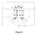
- FIG. 1A common port, represented here as a microstrip line 5 , ends at a point 6 near which several RF MEMS switches 10 - 1 through 10 - 4 are clustered.
- RF MEMS switches 10 - 1 through 10 - 4are preferably spaced equidistantly from a centerline of microstrip 5 and laterally on each side of it. Ports 1 , 2 , 3 , and 4 then spread out from this central point 6 , with each port being addressed by a single MEMS switch 10 .
- the substrateof which only a portion is shown, is represented by element 12 .
- RF energycan be directed from the common port provided by microstrip line 5 to the chosen selectable port (port 4 in this example) with very low loss.
- This switching circuitwill also demonstrate high isolation between the common port and the three open ports, as well as high isolation between each of the selectable ports.
- FIG. 1While the design depicted by FIG. 1 is believed to be novel, it has several flaws. Ideally, all four MEMS devices 10 - 1 through 10 - 4 should be clustered as close as reasonably possible around a single point 6 . In FIG. 1 , note that switches 10 have different spacings from end point 6 . When the switches 10 are separated by a length of transmission line, as is the case in FIG. 1 , that length of transmission line will then serve as a parasitic reactance to some of the ports. For example, in FIG. 1 , the length or portion of transmission line designated by the letter “L” appears as an open microstrip stub to ports 1 and 2 .
- This length L of microstrip 6is referred to as a “stub” in the antenna art and it affects the impedance of the circuit in which it appears.
- the effect, in this embodiment,is likely to be undesirable.
- the second pair of ports 3 , 4likely may not be brought any closer to the first pair 1 , 2 , because this would cause unwanted coupling between the closely spaced sections of microstrip line that would result.
- one wanted to compensate for the parasitic reactance caused by the microstrip stubone would need to separately tune each of the lines because they do not all see the same reactance. There may not be space on the top side of the circuit to allow a separate tuning element for each of the selectable ports, and still allow room for the DC bias lines and the RF signal lines.
- FIG. 1depicts a rather straightforward way of combining single-pole, single-throw RF MEMS switches into a single-pole, multi-throw hybrid design; however, the preferred designs are described with reference to the remaining figures.
- the inventionprovides a switch arrangement comprising a plurality of MEMS switches arranged on a substrate about a central point, each MEMS switch being disposed on a common imaginary circle centered on said central point, and each MEMS switch being spaced equidistantly along the circumference of said imaginary circle; and connections for connecting a RF port of each one of said MEMS switches with said central point.
- the inventionprovides a method of making a switch arrangement comprising: disposing a plurality of MEMS switches on a substrate in a circular pattern about a point; disposing a plurality of RF lines disposed in a radial pattern relative to said point on said substrate; and connecting said plurality of RF strip lines to a common junction point at said point on said substrate via said plurality of MEMS switches whereby operation of a one of said plurality of MEMS switches couples a one of said plurality of RF strip lines to said common junction.
- FIG. 1depicts one technique for combining single-pole, single-throw RF MEMS switches into a single-pole, multi-throw hybrid design
- FIGS. 2 a and 2 bare top and side elevation views of one embodiment of the present invention.
- FIGS. 3 a and 3 bare top and side elevation views of another embodiment of the present invention.
- FIG. 4shows a modification to the embodiment of FIGS. 3 a and 3 b;
- FIGS. 5 a and 5 bare top and side elevation views of yet another embodiment of the present invention.
- FIGS. 6 a and 6 bare top and side elevation views of still another embodiment of the present invention.
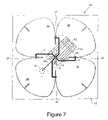
- FIG. 7depicts a switching arrangement of FIGS. 5 a and 5 b used in combination with a flared notch antenna
- FIG. 8depicts a switching arrangement of FIGS. 5 a and 5 b used in combination with a flared notch antenna having eight flared notch elements;
- FIG. 9depicts another improvement compared to the switch of FIG. 1 .
- FIG. 1Recall FIG. 1 and the fact that this design poses a number of problems in terms of the impedances seen from the common port of the microstrip line 6 when the various ports 1 - 4 are switched on.
- FIGS. 2 a and 2 bOne solution to this problem is shown in FIGS. 2 a and 2 b .
- Switches 10 - 1 through 10 - 4comprise a set of RF MEMS switches 10 (the numeral 10 when used without a dash and another numeral is used herein to refer to these RE MEMS switches in general as opposed to a particular switch). As will be seen, the number of switches 10 in the set can be greater than four, if desired.
- RF MEMS switches 10are positioned around common point 7 , preferably in a radial geometry as shown.
- the benefit of this geometryis that each of the selectable ports 1 - 4 sees the same RF environment (including the same impedance) by utilizing the same local geometry which is preferably only varied by rotation about an axis “A” defined through common point 7 . Therefore, each of the ports 1 - 4 should have the same RF performance (or, at least, nearly identical RF performances to each other). Furthermore, since this geometry permits the MEMS devices 10 to be clustered as closely as possible around common point 7 , parasitic reactance should be minimized.
- control line pairs 11can be arranged at right angles to each other, resulting in very low coupling between them.
- This embodimenthas four ports, but, as will be seen, this basic design can be modified to provide a greater (or lesser) number of ports.
- the MEMS switches 10are preferably disposed in a circular arrangement around central point 7 on substrate 12 .
- the switches 10lie on a circular arrangement as indicated by the circular line identified by the letter B.
- the switchesare preferably arranged equidistantly along the circumference of the circular line identified by the letter B.
- the MEMS switches 10can be placed individually directly on surface 9 of the circuit board 12 or they may be formed on a small substrate (not shown) as a switch hybrid, which is in turn mounted on surface 9 .
- Via 20preferably has a pad 8 on the top surface of the printed circuit board 12 to which the MEMS switches 10 can be wired, for example, using ball bonding techniques.
- the switches 10are also wired to the control lines pairs 11 and to the ports 1 - 4 .
- a common port 7is fed from the underside of the ground plane through a vertical metal plated via 20 to the top side of the board 12 where it terminates at central point 7 .
- MEMS switches 10are radially clustered around this central point.
- the centers of the MEMS switches 10are preferably spaced a common distance (a common radius) away from an axis A of the via 20 . This allows a large number of switches 10 to be fit into a small area, yet allows the coupling between the ports to be minimized.
- the couplingis further minimized by the fact that the RF microstrip lines directed to ports 1 - 4 are disposed at right angles to each other.
- the substrate 12 of this structurepreferably is a multi-layer microwave substrate with a buried ground plane 18 .
- the RF microstrip lines coupling to ports 1 - 4may form the driven elements of an antenna structure, for example, or may be coupled to antenna elements. Such elements may be used for sending and/or receiving RF signals.
- FIGS. 3 a and 3 bshow another embodiment of the present invention, in which some of the DC bias lines are implemented as vias 21 which connect with the buried ground plane 18 in substrate 12 .
- the vias 21may have pads 8 formed on their top surfaces in order to facilitate connecting the ground connections on the MEMS switches 10 thereto. Since each bias line pair 11 consists of a ground line 24 and a signal or control line 23 , each of the ground lines 24 - 1 - 24 - 4 , may be tied to the RF ground plane 18 , with no loss of performance, by means of vias 21 .
- FIG. 4An additional possible advantage of the geometry of FIGS. 3 a and 3 c is shown in FIG. 4 .
- a feed-through via 20such as that used for the common port 7 can sometimes have its own parasitic reactance.
- a complementary reactance Zas an external lumped element 25 , one may optimize the RF match of the circuit.
- the reactance Zcouples via 20 to ground using one of the vias 21 coupled to ground plane 18 . Since the impedance match is done on the central port 7 , and all other ports are symmetrical, the same matching structure Z will work for all of the ports.
- This lumped element solutionis one example of a matching structure, and others will be apparent to those skilled in the art of RF design.
- the ground connections of the MEMS switches 10are wired to metal plated vias 21 directly or to their associated pads 8 , either of which is in electrical communication with the buried ground plane 18 .
- the via 20 that provides the central RF portpasses through a hole or opening 19 in the ground plane 18 , while the vias 21 contact the ground plane 18 .
- the plurality of MEMS switch devices 10 - 1 10 - 4 of FIGS. 3 a , 3 b and 4are arranged on substrate 12 about a vertical axis A through the substrate, each switch 10 being disposed in a circular arrangement centered on axis A (central point 7 ) with each switch 10 being preferably spaced equidistantly along the circumference of the imaginary circle B defining the circular arrangement.
- the MEMS switches 10are preferably disposed in a circular arrangement around central point 7 on substrate 12 .
- the switches 10lie on indicated by the circular line identified by the letter B.
- the switchesare preferably arranged equidistantly along the circumference of the circular line identified by the letter B.
- the DC control lines 11 and 22are depicted as being thinner than are the RE lines 14 . If the DC lines are much thinner than the RE lines, they will have a higher impedance and coupling with the RF lines will be thereby reduced. While the percentage by which the DC are made thinner than the RE lines is somewhat a matter of tradeoffs, it is believed their width should preferably be about 25% of the width of the RE lines or less. The DC lines should be separated by at least one RE line width from the RE lines to reduce unwanted coupling.
- the MEMS switchesmay be wired to their RE lines, DC control lines, ground pads or lines by means of wires 30 bonded to the respective switches 10 and their various lines and/or pads.
- both the DC bias switch control lines 23 , 24 associated with each switch 10are fed through vertical metal plated vias 21 , 26 .
- one of the lines (line 24 )is grounded by means of via 21 contacting ground plane 18 and the other line (line 23 ) is connected, by means of a via 26 through a hole in the ground plane 18 , to a trace 27 on the back side of the board 12 which functions as a MEMS switch 10 control line.
- all of the DC bias lines 11pass through metal plated vias 21 , 26 . Half of them contact the ground plane 18 and the other half pass through the ground plane to contact traces 27 on the bottom or back side 13 of the board 12 .
- the RF and DC signalsshare lines 1 , 2 , 3 , 4 .
- Both the RF and the DC ports of the MEMS switches 10 - 1 . . . 10 - 4are connected together, as shown in FIG. 6 a .
- the DC portion of the signalmay be separated from the RF portion by using an inductor 32 - 1 . . . 32 - 4 in each of the switches' DC circuit.
- Thismay be either a lumped element, a printed inductor, or an inductive structure such as a very high-impedance RF line.
- Another inductor 34may be needed to separate the RF signal from the DC ground as shown in FIG. 6 b .
- FIGS. 6 a and 6 bshow a four port arrangement, but it is to be understood that this modification would be more apt to be used where space constraints do not allow the other embodiments to be easily utilized.
- the radial switching structure described aboveis combined with a printed antenna structure which may or may not share the same substrate 12 .
- the printed antenna structure 40preferably includes four conductive cloverleaf elements 36 which define flared notch antennas 37 therebetween.
- the DC bias lines 11 a disposed on the back side of the board, as well as the common RF line 14 , also on the backside of the board,are shown in dashed lines.
- the selectable RF lines on the front side of the boardare shown in solid lines.
- the conductive cloverleaf elementsare preferably formed on one surface of board 12 using conventional printed circuit board fabrication techniques.
- the cloverleaf elements 36may be made by appropriately etching a copper-clad printed circuit board, for example.
- the lines on the bottom side(shown dashed) can be similarly made by appropriately etching a copper-clad printed circuit board.
- Each flared notch 37is fed by a separate microstrip line 1 - 4 , each of which crosses over the notch of an antenna and is shorted to the ground plane 18 (see, e.g., FIG. 5 b ) on the opposite side of board 12 at vias 39 .
- These microstrip linescorrespond to the similarly numbered ports 1 - 4 discussed with respect to the switch arrangements of the earlier mentioned figures. RE energy passing down these microstrip lines is radiated from the associated antenna structure in a direction that antenna is pointing (i.e. along the mid-points of the notch of the notch antenna which is excited).
- the DC bias lines 11 and 11 aare preferably routed to a common connector 42 on the bottom side of the board 12 and the RF input preferably comprises a single feed point 41 which is routed to one of the four antenna structures (by means of one of the microstrips 1 - 4 ) as determined by which MEMS switch 10 (see FIG. 5 a the switches 10 are too small to be shown clearly on FIG. 7 , but they are clustered around point 7 ) is closed.
- Bias lines 11are disposed on the top side of board 12 while bias lines 11 a are disposed on the bottom side thereof. They are coupled together through the board 12 by means of vias. A pad 8 of one via is numbered in FIG.
- FIG. 7(the other vias are unnumbered due to the limited space available around them for reference numerals, but the vias can, nevertheless, be easily seen).
- the vias in FIG. 7are shown spaced further from the center point 7 than they would be in an actual embodiment, merely for ease of illustration.
- FIG. 8An embodiment more complicated than that of FIG. 7 is shown in FIG. 8 .
- This embodimenthas eight flared notches 37 defined by cloverleaf elements 36 and a single 1 ⁇ 8 array of RF MEMS switches 10 at the central point 7 (see FIG. 5 a —the switches 10 are again too small to be shown easily on FIG. 8 , but they are nevertheless clustered around central point 7 ).
- This antennauses the 1 ⁇ 8 MEMS switch to route the common input port to one of eight flared notch antennas 37 .
- This drawingonly shows the general concept of the structure and does not show the required DC bias lines or inductors. But those bias lines would be similar to those shown in FIG. 7 , but more numerous given the fact that this embodiment has eight notches 37 rather than four notches 37 .
- FIGS. 7 and 8demonstrate that the matrix of single-pole, multi-throw MEMS switches can be combined with an antenna structure 40 to create a switched beam diversity antenna of rather inexpensive components.
- the structure shown by FIG. 7uses four flared notches 37 , which are addressed by a 1 ⁇ 4 MEMS switch matrix preferably arranged in the radial configuration described above.
- FIGS. 3 a and 3 bThe preferred embodiment of the hybrid single-pole, multi-throw switch has been described with reference to FIGS. 3 a and 3 b . It is felt that this embodiment can be rather easily manufactured.
- the antenna cloverleaf design of FIG. 8is preferred since eight slots provide good diversity control.
- FIG. 9One such solution is shown in FIG. 9 .
- FIG. 9is not a presently preferred embodiment of this invention, but it is an embodiment that may have sufficient advantages in certain applications, such as when metal plated vias cannot be used, that some practicing the present invention may choose to utilize it. This may be the case when a monolithic approach is taken, when vias and internal ground layers may not be feasible or may not be simple to realize.
- This embodimentbuilds on the concept that the individual MEMS devices 10 are preferably clustered as closely as possible around a central point 7 to avoid parasitic reactance. This embodiment also recognizes that this may not be possible for a design to have a large number of ports, because when the microstrip transmission lines are brought too close to each other, unwanted coupling occurs.
- a 1 ⁇ 3 switching unit SUis used as a building block for a 1 ⁇ N switch of any desired size.
- Each SUhas a pair of MEMS switches 10 for coupling the transmission lines to a central point 7 of the SU.
- Each transmission line port 1 , 2 of a first unitis accessed through a MEMS device 10
- subsequent transmission line portsfor example, ports 3 , 4 of a second SU
- third MEMS device(s) 45which route the RF signals along sections of central transmission line 46 (which may now be of any length required to minimize coupling between ports) to a next 1 ⁇ 3 switching unit SU.
- Each switching unit SUcomprises two (or possibly more) MEMS switches 10 clustered around its own central point 7 for coupling the transmission lines thereto and another MEMS switch 45 for passing the incoming signal to yet another switching unit SU.
- two additional (or more) transmission linesmay be addressed each through their own individual MEMS device 10 , or the signals may be sent to the next SU through the third MEMS device 45 . Since unused sections of transmission line are switched off when they are not used, they do not present unwanted parasitic reactance. Of course, all of the DC bias methods described in previous embodiments may be applied to this structure as well.
- FIG. 9thus depicts an alternate design that may be used if a central metal-plated via 20 feature of the earlier embodiments is not feasible.
- the design of FIG. 9uses a 1 ⁇ 3 switch SU as a building block for a 1 ⁇ N switch of any size. It benefits from the knowledge that dangling sections of RF line will cause parasitic reactance when they are not used.
- the third switch 45is opened if one of the ports on that unit is selected by means of closing its associated MEMS switch 10 . If neither switch 10 is selected, the third switch 45 is closed, and the signal is routed to the next SU.
- the MEMS switches 10are preferably disposed in a circular arrangement around central point 7 .
- the switches 10 , 45also preferably lie on an imaginary circle, here again identified by the letter B.
- the switches 10 , 45 and segment 46are preferably arranged equidistant ly along the circumference identified by the letter B.
- the first portionrefers to the element type (a MEMS switch in this case) and the second portion (the 2 in this case) refer to a particular one of those elements (a second MEMS switch 10 in this case).
- This numbering schemeis likely self-explanatory, but it is nevertheless here explained for the reader who might not have previously encountered it.
- the MEM switches 10 - 1 . . . 10 - 4 and 45may be provided with integral impedance matching elements, such as capacitors, in order to increase the return loss to more than 20 dB. For that reason, the MEM switches disclosed by U.S. Provisional Patent Application Ser. No. 60/470,026 filed May 12, 2003 and entitled “RF MEMS Switch with Integrated Impedance Matching Structure” are believed to be the preferred MEM switches for use in connection with this invention.
Landscapes
- Waveguide Switches, Polarizers, And Phase Shifters (AREA)
- Variable-Direction Aerials And Aerial Arrays (AREA)
- Superconductor Devices And Manufacturing Methods Thereof (AREA)
Abstract
Description
This application claims the benefit of U.S. Provisional Patent Application No. 60/381,099 filed on May 15, 2002, which application is incorporated herein by reference.
This invention relates to single-pole, multi-throw switches that are built using single-pole, single-throw devices combined in a hybrid circuit. The switches of this invention are symmetrically located around a central point which is a vertical via in a multi layer printed circuit board.
This application incorporates by reference the disclosure of U.S. Provisional Patent Application Ser. No. 60/470,026 filed May 12, 2003 and entitled “RE MEMS Switch with Integrated Impedance Matching Structure”.
In one aspect, this invention addresses several problems with existing single-pole, multi-throw switches built using single-pole, single-throw devices preferably combined in a switch matrix. According to this aspect of the invention, the switches are symmetrically located around a central point which is preferably a vertical via in a multi layer printed circuit board. In this way, a maximum number of switches can be located around the common port with a minimum amount of separation. This leads to the lowest possible parasitic reactance, and gives the circuit the greatest possible frequency response. Furthermore, any residual parasitic reactance can be matched by a single element on the common port, so that all ports will have the same frequency response. This patent describes a 1×4 switch, but the concept may be extended to a 1×6 switch or to a 1×8 switch or a switch with even greater fan out (1×N). Also, such a switch can be integrated with an antenna array for the purpose of producing a switched beam diversity antenna.
The switch arrangement disclosed herein can be conveniently used with a Vivaldi Cloverleaf Antenna to determine which antenna of the Vivaldi Cloverleaf Antenna is active. U.S. patent application Ser. No. 09/525,832 entitled “Vivaldi Cloverleaf Antenna” filed Mar. 12, 2000, the disclosure of which is hereby incorporated herein by this reference, teaches how Vivaldi Cloverleaf Antennas may be made.
The present invention has a number of possible applications and uses. As a basic building block in any communication system, and in microwave systems in general, a single-pole, multi-throw radio frequency switch has numerous applications. As communication systems get increasingly complicated, and they require diversity antennas, reconfigurable receivers, and space time processing, the need for more sophisticated radio frequency components will grow. These advanced communications systems will need single-pole multi-throw switches having low parasitic reactance. Such switches will be used, for example, in connection with the antenna systems of these communication systems.
The prior art includes the following:
- (1) M. Ando, “Polyhedral Shaped Redundant Coaxial Switch”, U.S. Pat. No. 6,252,473 issued Jun. 26, 2001 and assigned to Hughes Electronics Corporation. This patent describes a waveguide switch using bulk mechanical actuators.
- (2) B. Mayer, “Microwave Switch with Grooves for Isolation of the Passages”, U.S. Pat. No. 6,218,912 issued Apr. 17, 2001 and assigned to Robert Bosch GmbH. This patent describes a waveguide switch with a mechanical rotor structure.
Neither of the patents noted above address issues that are particular to the needs of a single-pole multi-throw switch of the type disclosed herein. Although they are of a radial design, they are built using a conventional waveguide rather than (i) MEM devices and (ii) microstrips. It is not obvious that a radial design could be used for a MEM device switch and/or a microstrip switch because the necessary vertical through-ground vias are not commonly used in microstrip circuits. Furthermore, the numerous examples of microstrip switches available in the commercial marketplace do not directly apply to this invention because they typically use PIN diodes or FET switches, which carry certain requirements for the biasing circuit that dictate the geometry and which are not convenient for use in a radial design.
There is a need for single-pole, multi-throw switches as a general building block for radio frequency communication systems. One means of providing such devices that have the performance required for modern Radio Frequency (RF) systems is to use RF Micro Electro-Mechanical System (MEMS) switches. One solution to this problem would be to simply build a 1×N monolithic MEMS switch on a single substrate. However, there may be situations in which this is not possible, or when one cannot achieve the required characteristics in a monolithic solution, such as a large fan-out number for example. In these situations, a hybrid approach should be used.
There are numerous ways to assemble single-pole, single-throw RF MEMS switches on a microwave substrate, along with RF lines to create the desired switching circuit. Possibly the most convenient way is shown inFIG. 1 . A common port, represented here as amicrostrip line 5, ends at a point6 near which several RF MEMS switches10-1 through10-4 are clustered. RF MEMS switches10-1 through10-4 are preferably spaced equidistantly from a centerline ofmicrostrip 5 and laterally on each side of it.Ports single MEMS switch 10. The substrate, of which only a portion is shown, is represented byelement 12. By closing one of the switches (for example, switch10-4), and opening all of the others (for example, switches10-1 through10-3), RF energy can be directed from the common port provided bymicrostrip line 5 to the chosen selectable port (port 4 in this example) with very low loss. This switching circuit will also demonstrate high isolation between the common port and the three open ports, as well as high isolation between each of the selectable ports.
While the design depicted byFIG. 1 is believed to be novel, it has several flaws. Ideally, all four MEMS devices10-1 through10-4 should be clustered as close as reasonably possible around a single point6. InFIG. 1 , note thatswitches 10 have different spacings from end point6. When theswitches 10 are separated by a length of transmission line, as is the case inFIG. 1 , that length of transmission line will then serve as a parasitic reactance to some of the ports. For example, inFIG. 1 , the length or portion of transmission line designated by the letter “L” appears as an open microstrip stub toports ports first pair
In one aspect, the invention provides a switch arrangement comprising a plurality of MEMS switches arranged on a substrate about a central point, each MEMS switch being disposed on a common imaginary circle centered on said central point, and each MEMS switch being spaced equidistantly along the circumference of said imaginary circle; and connections for connecting a RF port of each one of said MEMS switches with said central point.
In another aspect, the invention provides a method of making a switch arrangement comprising: disposing a plurality of MEMS switches on a substrate in a circular pattern about a point; disposing a plurality of RF lines disposed in a radial pattern relative to said point on said substrate; and connecting said plurality of RF strip lines to a common junction point at said point on said substrate via said plurality of MEMS switches whereby operation of a one of said plurality of MEMS switches couples a one of said plurality of RF strip lines to said common junction.
RecallFIG. 1 and the fact that this design poses a number of problems in terms of the impedances seen from the common port of the microstrip line6 when the various ports1-4 are switched on. One solution to this problem is shown inFIGS. 2 aand2b. The structure ofFIGS. 2 aand2bpreferably consists of a multi-layer printedcircuit board 12, on which acommon RF line 14 is formed on the bottom or backside 13 of theboard 12, and is fed through aground plane 18 by a metal plated via20 to acentral point 7 in the center of a 1×4 switch matrix of switches10-1 through10-4, which switches may be made as a hybrid on a common substrate (not shown) or which may be individually attached tosurface 9. Switches10-1 through10-4 comprise a set of RF MEMS switches10 (the numeral10 when used without a dash and another numeral is used herein to refer to these RE MEMS switches in general as opposed to a particular switch). As will be seen, the number ofswitches 10 in the set can be greater than four, if desired.
RF MEMS switches10 are positioned aroundcommon point 7, preferably in a radial geometry as shown. The benefit of this geometry is that each of the selectable ports1-4 sees the same RF environment (including the same impedance) by utilizing the same local geometry which is preferably only varied by rotation about an axis “A” defined throughcommon point 7. Therefore, each of the ports1-4 should have the same RF performance (or, at least, nearly identical RF performances to each other). Furthermore, since this geometry permits theMEMS devices 10 to be clustered as closely as possible aroundcommon point 7, parasitic reactance should be minimized. Moreover, for the case of a 1×4 switch matrix, control line pairs11 can be arranged at right angles to each other, resulting in very low coupling between them. This embodiment has four ports, but, as will be seen, this basic design can be modified to provide a greater (or lesser) number of ports.
The MEMS switches10 are preferably disposed in a circular arrangement aroundcentral point 7 onsubstrate 12. Note that theswitches 10 lie on a circular arrangement as indicated by the circular line identified by the letter B. Note also that the switches are preferably arranged equidistantly along the circumference of the circular line identified by the letter B. The MEMS switches10 can be placed individually directly onsurface 9 of thecircuit board 12 or they may be formed on a small substrate (not shown) as a switch hybrid, which is in turn mounted onsurface 9.
Via20 preferably has apad 8 on the top surface of the printedcircuit board 12 to which the MEMS switches10 can be wired, for example, using ball bonding techniques. Theswitches 10 are also wired to the control lines pairs11 and to the ports1-4.
InFIG. 2 acommon port 7 is fed from the underside of the ground plane through a vertical metal plated via20 to the top side of theboard 12 where it terminates atcentral point 7. MEMS switches10 are radially clustered around this central point. The centers of the MEMS switches10 are preferably spaced a common distance (a common radius) away from an axis A of the via20. This allows a large number ofswitches 10 to be fit into a small area, yet allows the coupling between the ports to be minimized. In the particular case of the 1×4 switch, with MEMS switches10-1-10-4, the coupling is further minimized by the fact that the RF microstrip lines directed to ports1-4 are disposed at right angles to each other. Thesubstrate 12 of this structure preferably is a multi-layer microwave substrate with a buriedground plane 18.
The RF microstrip lines coupling to ports1-4 may form the driven elements of an antenna structure, for example, or may be coupled to antenna elements. Such elements may be used for sending and/or receiving RF signals.
An additional possible advantage of the geometry ofFIGS. 3 aand3cis shown inFIG. 4 . A feed-through via20 such as that used for thecommon port 7 can sometimes have its own parasitic reactance. By providing a complementary reactance Z as an external lumpedelement 25, one may optimize the RF match of the circuit. InFIG. 4 the reactance Z couples via20 to ground using one of thevias 21 coupled toground plane 18. Since the impedance match is done on thecentral port 7, and all other ports are symmetrical, the same matching structure Z will work for all of the ports. This lumped element solution is one example of a matching structure, and others will be apparent to those skilled in the art of RF design. The ground connections of the MEMS switches10 are wired to metal platedvias 21 directly or to their associatedpads 8, either of which is in electrical communication with the buriedground plane 18. Note that the via20 that provides the central RF port passes through a hole or opening19 in theground plane 18, while thevias 21 contact theground plane 18.
As in the case ofFIGS. 2 aand2b, the plurality of MEMS switch devices10-110-4 ofFIGS. 3 a,3band4 are arranged onsubstrate 12 about a vertical axis A through the substrate, eachswitch 10 being disposed in a circular arrangement centered on axis A (central point7) with eachswitch 10 being preferably spaced equidistantly along the circumference of the imaginary circle B defining the circular arrangement. Thus, the MEMS switches10 are preferably disposed in a circular arrangement aroundcentral point 7 onsubstrate 12. Note that theswitches 10 lie on indicated by the circular line identified by the letter B. Note also that the switches are preferably arranged equidistantly along the circumference of the circular line identified by the letter B.
InFIGS. 2 aand3atheDC control lines 11 and22 are depicted as being thinner than are the RE lines14. If the DC lines are much thinner than the RE lines, they will have a higher impedance and coupling with the RF lines will be thereby reduced. While the percentage by which the DC are made thinner than the RE lines is somewhat a matter of tradeoffs, it is believed their width should preferably be about 25% of the width of the RE lines or less. The DC lines should be separated by at least one RE line width from the RE lines to reduce unwanted coupling. The MEMS switches may be wired to their RE lines, DC control lines, ground pads or lines by means of wires30 bonded to therespective switches 10 and their various lines and/or pads.
Yet another embodiment of this structure is shown inFIGS. 5 aand5b. In this embodiment, both the DC bias switch control lines23,24 associated with eachswitch 10 are fed through vertical metal platedvias switch 10, one of the lines (line24) is grounded by means of via21 contactingground plane 18 and the other line (line23) is connected, by means of a via26 through a hole in theground plane 18, to atrace 27 on the back side of theboard 12 which functions as aMEMS switch 10 control line. This reduces clutter (lines which do not directly assist the RF capabilities of the switch arrangement) on the front of the board, and can allow for more complex switching circuits and for reduced coupling between the RF lines and the DC bias lines11.
In the embodiment ofFIGS. 5 aand5b, all of the DC bias lines11 pass through metal platedvias ground plane 18 and the other half pass through the ground plane to contacttraces 27 on the bottom or backside 13 of theboard 12.
Several geometries have been described which are based on a common theme of a radial switching structure, with discreteRF MEMS devices 10 assembled around acommon input port 7 ofmicrostrip line 14, and routing RF energy to one of several output ports (for example, ports1-4 in a four port embodiment).
It should be understood that the operation of the disclosed device is reciprocal, in that the various ports described as the output ports could also serve as a plurality of alternate input ports which are fed to a common output port which is thecentral point 7. Furthermore, it should be understood that although 1×4 switching circuits have been shown, other numbers of switches in the switching circuits are possible such as 1×6 and 1×8 and possibly even higher numbers, and that these designs will be apparent to one skilled in the art of RF design after fully understanding the disclosure of this patent document. However, a large number of ports may be difficult to realize due to crowding of the RF lines and he DC bias lines. This issue can be addressed by using the modification shown inFIGS. 6 aand6b. In this embodiment, the RF and DC signals sharelines FIG. 6 a. The DC portion of the signal may be separated from the RF portion by using an inductor32-1 . . .32-4 in each of the switches' DC circuit. This may be either a lumped element, a printed inductor, or an inductive structure such as a very high-impedance RF line. Anotherinductor 34 may be needed to separate the RF signal from the DC ground as shown inFIG. 6 b. In that case, the end ofinductor 34 remote from the connection to via20 is coupled to aline 15 at ground potential. If it is necessary to prevent the DC signal from reaching other RF components, then an external DC blocking capacitor may be used on each of the RF lines. These capacitors are not shown in the figures.FIGS. 6 aand6bshow a four port arrangement, but it is to be understood that this modification would be more apt to be used where space constraints do not allow the other embodiments to be easily utilized.
In another aspect of this invention, the radial switching structure described above is combined with a printed antenna structure which may or may not share thesame substrate 12. In the embodiment ofFIG. 7 , the printedantenna structure 40 preferably includes fourconductive cloverleaf elements 36 which define flarednotch antennas 37 therebetween. The DC biaslines 11adisposed on the back side of the board, as well as thecommon RF line 14, also on the backside of the board, are shown in dashed lines. The selectable RF lines on the front side of the board are shown in solid lines. The conductive cloverleaf elements are preferably formed on one surface ofboard 12 using conventional printed circuit board fabrication techniques. Thus, thecloverleaf elements 36 may be made by appropriately etching a copper-clad printed circuit board, for example. The lines on the bottom side (shown dashed) can be similarly made by appropriately etching a copper-clad printed circuit board.
Each flarednotch 37 is fed by a separate microstrip line1-4, each of which crosses over the notch of an antenna and is shorted to the ground plane18 (see, e.g.,FIG. 5 b) on the opposite side ofboard 12 atvias 39. These microstrip lines correspond to the similarly numbered ports1-4 discussed with respect to the switch arrangements of the earlier mentioned figures. RE energy passing down these microstrip lines is radiated from the associated antenna structure in a direction that antenna is pointing (i.e. along the mid-points of the notch of the notch antenna which is excited). The DC biaslines common connector 42 on the bottom side of theboard 12 and the RF input preferably comprises asingle feed point 41 which is routed to one of the four antenna structures (by means of one of the microstrips1-4) as determined by which MEMS switch10 (seeFIG. 5 atheswitches 10 are too small to be shown clearly onFIG. 7 , but they are clustered around point7) is closed.Bias lines 11 are disposed on the top side ofboard 12 while bias lines11aare disposed on the bottom side thereof. They are coupled together through theboard 12 by means of vias. Apad 8 of one via is numbered inFIG. 7 (the other vias are unnumbered due to the limited space available around them for reference numerals, but the vias can, nevertheless, be easily seen). The vias inFIG. 7 are shown spaced further from thecenter point 7 than they would be in an actual embodiment, merely for ease of illustration.
An embodiment more complicated than that ofFIG. 7 is shown inFIG. 8 . This embodiment has eight flarednotches 37 defined by cloverleafelements 36 and a single 1×8 array of RF MEMS switches10 at the central point7 (seeFIG. 5 a—theswitches 10 are again too small to be shown easily onFIG. 8 , but they are nevertheless clustered around central point7). This antenna uses the 1×8 MEMS switch to route the common input port to one of eight flarednotch antennas 37. This drawing only shows the general concept of the structure and does not show the required DC bias lines or inductors. But those bias lines would be similar to those shown inFIG. 7 , but more numerous given the fact that this embodiment has eightnotches 37 rather than fournotches 37.
The preferred embodiment of the hybrid single-pole, multi-throw switch has been described with reference toFIGS. 3 aand3b. It is felt that this embodiment can be rather easily manufactured. The antenna cloverleaf design ofFIG. 8 is preferred since eight slots provide good diversity control. However, there may be other embodiments, and other ways of solving the problems associated with the candidate structure described with reference toFIG. 1 . One such solution is shown inFIG. 9 .
The embodiment ofFIG. 9 is not a presently preferred embodiment of this invention, but it is an embodiment that may have sufficient advantages in certain applications, such as when metal plated vias cannot be used, that some practicing the present invention may choose to utilize it. This may be the case when a monolithic approach is taken, when vias and internal ground layers may not be feasible or may not be simple to realize. This embodiment builds on the concept that theindividual MEMS devices 10 are preferably clustered as closely as possible around acentral point 7 to avoid parasitic reactance. This embodiment also recognizes that this may not be possible for a design to have a large number of ports, because when the microstrip transmission lines are brought too close to each other, unwanted coupling occurs. To address both of these problems, a 1×3 switching unit SU is used as a building block for a 1×N switch of any desired size. Each SU has a pair of MEMS switches10 for coupling the transmission lines to acentral point 7 of the SU. Eachtransmission line port MEMS device 10, while subsequent transmission line ports (for example,ports central point 7 for coupling the transmission lines thereto and anotherMEMS switch 45 for passing the incoming signal to yet another switching unit SU. In this and in each subsequent block SU, two additional (or more) transmission lines may be addressed each through their ownindividual MEMS device 10, or the signals may be sent to the next SU through thethird MEMS device 45. Since unused sections of transmission line are switched off when they are not used, they do not present unwanted parasitic reactance. Of course, all of the DC bias methods described in previous embodiments may be applied to this structure as well. Furthermore, other structures that use the 1×3 building block in this way, to allow necessary but unwanted sections of transmission lines to be turned off when not in use, will be apparent after this invention is understood. One example of another design would be a corporate switching structure, as opposed to the linear one presented here. In a corporate structure one input feeds two outputs, each of which in turn feed two more outputs, and those outputs each in turn feed two more outputs, until you have 2noutputs at the end. When it is drawn, it looks like a corporate organization chart with many layers of middle management (hence the name).
The MEMS switches10 are preferably disposed in a circular arrangement aroundcentral point 7. Note that in this embodiment theswitches switches segment 46 are preferably arranged equidistant ly along the circumference identified by the letter B.
In the numbering of the elements in this description and in the drawings, numbers such as 10-2 appear. The first portion (the 10 in this case) refers to the element type (a MEMS switch in this case) and the second portion (the 2 in this case) refer to a particular one of those elements (asecond MEMS switch 10 in this case). This numbering scheme is likely self-explanatory, but it is nevertheless here explained for the reader who might not have previously encountered it.
The MEM switches10-1 . . .10-4 and45 may be provided with integral impedance matching elements, such as capacitors, in order to increase the return loss to more than 20 dB. For that reason, the MEM switches disclosed by U.S. Provisional Patent Application Ser. No. 60/470,026 filed May 12, 2003 and entitled “RF MEMS Switch with Integrated Impedance Matching Structure” are believed to be the preferred MEM switches for use in connection with this invention.
Having described the invention in connection with certain embodiments thereof, modification will now certainly suggest itself to those skilled in the art. A such, the invention is not to be limited to the disclosed embodiments except as required by the appended claims.
Claims (39)
1. A switch arrangement comprising:
(a) a plurality of MEMS switches arranged on a substrate about an axis through said substrate, each MEMS switch being disposed on a common imaginary circle centered on said axis, and each MEMS switch being spaced equidistantly along the circumference of said imaginary circle;
(b) a conductive via in said substrate arranged parallel to and on said axis; and
(c) connections for connecting a RF port of each one of said plurality of MEMS switches with said conductive via.
2. The switch arrangement ofclaim 1 wherein the substrate has a ground plane therein, said conductive via passing through said ground plane without contacting said ground plane.
3. The switch arrangement ofclaim 2 further including a plurality of strip lines, each one of said plurality of strip lines being coupled to a RF contact of one of said plurality of MEMS switches.
4. The switch arrangement ofclaim 3 wherein said plurality of strip lines are radially arranged relative to said axis.
5. The switch arrangement ofclaim 4 wherein said plurality of strip lines and said plurality of MEMS switches are disposed on a first major surface of said substrate.
6. The switch arrangement ofclaim 5 further including a plurality of control lines disposed on said first major surface of said substrate, each control line being coupled to an associated one of said plurality of MEMS switches and being disposed between two adjacent strip lines.
7. The switch arrangement ofclaim 6 wherein each of the plurality of control lines has a first width and wherein each of the plurality of strip lines has a second width, the second width being at least three times greater than the first width.
8. The switch arrangement ofclaim 6 further including a plurality of conductive vias in said substrate arranged parallel to said axis and contacting said ground plane, each of said plurality of MEMS switches having a DC ground contact which is wired to one of the plurality of conductive vias contacting said ground plane.
9. The switch arrangement ofclaim 8 further including an impedance device coupling the conductive via on the central point to one of the plurality of conductive vias, the impedance device being disposed adjacent a second major surface of said substrate.
10. The switch arrangement ofclaim 5 further including a plurality of control lines arranged in pairs and disposed on said first major surface of said substrate, each control line pair being coupled to an associated one of said plurality of MEMS switches and being disposed between two adjacent strip lines.
11. The switch arrangement ofclaim 10 wherein each of the plurality of control lines has a first width and wherein each of the plurality of strip lines has a second width, the second width being at least three times greater than the first width.
12. A switch arrangement comprising a plurality of switch units, each switch unit having at least two MEMS switches coupled to a first central point, the at least two MEMS switches of the switch unit being arranged to couple selectively at least two co-linear transmission line ports to said first central point, and at least a third MEMS switch coupled to said first central point and adapted to be connected to a second central point different from said first central point, said second central point associated with an adjacent one of said plurality of switch units.
13. The switch arrangement ofclaim 12 wherein each switch unit has a centrally disposed transmission line, the centrally disposed transmission line connecting the switch unit to the at least a third MEMS switch associated with an adjacent one of said plurality of switch units.
14. The switch arrangement ofclaim 13 wherein the centrally disposed transmission line is linearly arranged from a central point of each switch unit towards the at least a third MEMS switch associated with an adjacent one of said plurality of switch units.
15. The switch arrangement ofclaim 12 wherein the at least two transmission line ports are arranged to couple antennas to said at least two MEMS switches.
16. A switch arrangement comprising:
(a) a plurality of MEMS switches arranged on a substrate about a central point, each MEMS switch being disposed on a common imaginary circle centered on said central point, and each MEMS switch being spaced equidistantly along the circumference of said imaginary circle; and
(b) connections for connecting a RE port of each one of said MEMS switches with said central point, wherein at least two of the MEMS switches are arranged to couple selectively at least two transmission lines to said central point and wherein a pair of the at least two transmission lines are disposed co-linearly of each other.
17. The switch arrangement ofclaim 16 wherein at least one of the MEMS switches is arranged to couple selectively the central point of the switch arrangement to a central point associated with another switch arrangement via a transmission line segment.
18. The switch arrangement ofclaim 16 wherein the substrate has a ground plane therein and the switch arrangement further includes a conductive via in said substrate arranged parallel to and on a vertical axis which is normal to a major surface of substrate and which passes through said central point, the conductive via passing through said ground plane without contacting same.
19. The switch arrangement ofclaim 18 further including a plurality of strip lines, each one of said plurality of strip lines being coupled to a RF contact of one of said plurality of MEMS switches.
20. The switch arrangement ofclaim 19 wherein said plurality of strip lines are radially arranged relative to said central point.
21. The switch arrangement ofclaim 20 wherein said plurality of strip lines and said plurality of MEMS switches are disposed on a first major surface of said substrate.
22. The switch arrangement ofclaim 21 further including a plurality of control lines disposed on said first major surface of said substrate, each control line being coupled to an associated one of said plurality of MIEMS switches and being disposed between two adjacent strip lines of said plurality of strip lines.
23. The switch arrangement ofclaim 22 further including a plurality of conductive vias in said substrate arranged parallel to said axis and contacting said ground plane, each of said plurality of MEMS switches having a DC ground contact which is wired to a one of a plurality of conductive vias contacting said ground plane.
24. The switch arrangement ofclaim 23 further including an impedance device coupling a conductive via on the central point to one of the plurality of conductive vias, the impedance device being disposed adjacent a second major surface of said substrate.
25. The switch arrangement ofclaim 21 further including a plurality of control lines arranged in pairs and disposed on said first major surface of said substrate, each control line pair being coupled to an associated one of said plurality of MEMS switches and being disposed between two adjacent strip lines of said plurality of strip lines.
26. An antenna comprising a plurality of end fire Vivaldi antennas arranged in a cloverleaf configuration in combination with the switch arrangement ofclaim 16 for controlling which one or ones of said plurality of end fire Vivaldi antennas is or are active.
27. An antenna comprising a plurality of end fire Vivaldi antennas arranged in a cloverleaf configuration in combination with the switch arrangement ofclaim 16 for controlling which one of said plurality of end fire Vivaldi antennas is active.
28. A method of making a switch arrangement comprising:
(a) disposing a plurality of MEMS switches on a substrate in a circular pattern about a point;
(b) disposing a plurality of RE lines disposed in a radial pattern relative to said point on said substrate; and
(c) connecting said plurality of RE lines to a common junction point at said point on said substrate via said plurality of MEMS switches whereby operation of a one of said plurality of MEMS switches couples a one of said plurality of RF lines to said common junction, wherein at least two of the MEMS switches of said plurality of MEMS switches are arranged to couple selectively at least two RE lines to said point and wherein a pair of the at least two RF lines are disposed co-linearly of each other.
29. The method ofclaim 28 wherein at least one of the MEMS switches of said plurality of MEMS switches is arranged to couple selectively the common junction point to another common junction point associated with another switch arrangement made according to the method ofclaim 28 via a transmission line segment disposed on said substrate.
30. The method ofclaim 29 further including providing a ground plane in the substrate and providing a conductive via in said substrate arranged parallel to and on an axis through said point and normal to a major surface of said substrate, the conductive via passing through said ground plane without contacting same.
31. The method ofclaim 30 further including disposing a plurality of strip lines on said surface and coupling each one of said plurality of strip lines to a RF contact of one of said plurality of MEMS switches.
32. The method ofclaim 31 wherein said plurality of strip line and said plurality of MEMS switches are disposed on the first major surface of said substrate.
33. The method ofclaim 32 further including disposing a plurality of control lines on the first major surface of said substrate, each control line being coupled to an associated one of said plurality of MEMS switches and being disposed between two adjacent strip lines.
34. The method ofclaim 33 further including providing a plurality of conductive vias in said substrate arranged parallel to said axis and contacting said ground plane, each of said plurality of MEMS switches having a DC ground contact which is wired to a one of the plurality of conductive vias contacting said ground plane.
35. The method ofclaim 34 further including coupling an impedance device between (i) the conductive via connected to the common junction point and (ii) at least one of the plurality of conductive vias, the impedance device being disposed adjacent a second major surface of said substrate.
36. The method ofclaim 32 further including disposing a plurality of control lines arranged in pairs on the first major surface of said substrate, each control line pair being coupled to an associated one of said plurality of MEMS switches and being disposed between two adjacent strip lines.
37. A switch arrangement comprising:
(a) a plurality of MEMS switches arranged on a substrate about a common RE port, the RE port having a centerline and each MEMS switch being disposed spaced equidistantly from the centerline of said RE port; and
(b) connections for connecting a RE contact of each one of said MEMS switches with said common RE port, wherein at least two of the MEMS switches of said plurality of MEMS switches are arranged to couple selectively at least two RE lines to said RE port and wherein a pair of the at least two RE lines are disposed co-linearly of each other.
38. The switch arrangement ofclaim 37 wherein the centerline of the RE port is disposed perpendicular to a major surface of said substrate.
39. The switch arrangement ofclaim 37 wherein the centerline of the RE port is disposed parallel to a major surface of said substrate.
Priority Applications (2)
| Application Number | Priority Date | Filing Date | Title |
|---|---|---|---|
| US10/436,753US7298228B2 (en) | 2002-05-15 | 2003-05-12 | Single-pole multi-throw switch having low parasitic reactance, and an antenna incorporating the same |
| US10/714,528US7276990B2 (en) | 2002-05-15 | 2003-11-14 | Single-pole multi-throw switch having low parasitic reactance, and an antenna incorporating the same |
Applications Claiming Priority (2)
| Application Number | Priority Date | Filing Date | Title |
|---|---|---|---|
| US38109902P | 2002-05-15 | 2002-05-15 | |
| US10/436,753US7298228B2 (en) | 2002-05-15 | 2003-05-12 | Single-pole multi-throw switch having low parasitic reactance, and an antenna incorporating the same |
Related Child Applications (1)
| Application Number | Title | Priority Date | Filing Date |
|---|---|---|---|
| US10/714,528Continuation-In-PartUS7276990B2 (en) | 2002-05-15 | 2003-11-14 | Single-pole multi-throw switch having low parasitic reactance, and an antenna incorporating the same |
Publications (2)
| Publication Number | Publication Date |
|---|---|
| US20030227351A1 US20030227351A1 (en) | 2003-12-11 |
| US7298228B2true US7298228B2 (en) | 2007-11-20 |
Family
ID=29550069
Family Applications (1)
| Application Number | Title | Priority Date | Filing Date |
|---|---|---|---|
| US10/436,753Expired - Fee RelatedUS7298228B2 (en) | 2002-05-15 | 2003-05-12 | Single-pole multi-throw switch having low parasitic reactance, and an antenna incorporating the same |
Country Status (6)
| Country | Link |
|---|---|
| US (1) | US7298228B2 (en) |
| JP (2) | JP2005526433A (en) |
| AU (1) | AU2003232149A1 (en) |
| GB (1) | GB2404095B (en) |
| TW (1) | TWI244801B (en) |
| WO (1) | WO2003098732A1 (en) |
Cited By (26)
| Publication number | Priority date | Publication date | Assignee | Title |
|---|---|---|---|---|
| US20070060201A1 (en)* | 2005-09-14 | 2007-03-15 | Nagy Louis L | Self-structuring antenna with addressable switch controller |
| US20080106475A1 (en)* | 2004-04-29 | 2008-05-08 | Harris Corporation | Printed wiring board with enhanced structural integrity |
| US20080165061A1 (en)* | 2007-01-05 | 2008-07-10 | Advanced Connection Technology Inc. | Circularly polarized antenna |
| US20090220030A1 (en)* | 2008-02-28 | 2009-09-03 | Uhl Brecken H | System and method for modulating a signal at an antenna |
| US20100208771A1 (en)* | 2008-11-25 | 2010-08-19 | Uhl Brecken H | System and method for spreading and de-spreading a signal at an antenna |
| US20100208844A1 (en)* | 2008-11-25 | 2010-08-19 | Uhl Brecken H | System and method for arbitrary phase and amplitude modulation in an antenna |
| US20100207819A1 (en)* | 2008-11-25 | 2010-08-19 | Uhl Brecken H | System and method for electronically steering an antenna |
| US20100231473A1 (en)* | 2009-03-13 | 2010-09-16 | Victor Shtrom | Adjustment of Radiation Patterns Utilizing a Position Sensor |
| US20100302126A1 (en)* | 2004-11-22 | 2010-12-02 | Victor Shtrom | Antenna Array |
| US7893882B2 (en) | 2007-01-08 | 2011-02-22 | Ruckus Wireless, Inc. | Pattern shaping of RF emission patterns |
| US8068068B2 (en) | 2005-06-24 | 2011-11-29 | Ruckus Wireless, Inc. | Coverage antenna apparatus with selectable horizontal and vertical polarization elements |
| US8436785B1 (en) | 2010-11-03 | 2013-05-07 | Hrl Laboratories, Llc | Electrically tunable surface impedance structure with suppressed backward wave |
| US8525745B2 (en) | 2010-10-25 | 2013-09-03 | Sensor Systems, Inc. | Fast, digital frequency tuning, winglet dipole antenna system |
| US8756668B2 (en) | 2012-02-09 | 2014-06-17 | Ruckus Wireless, Inc. | Dynamic PSK for hotspots |
| US8982011B1 (en) | 2011-09-23 | 2015-03-17 | Hrl Laboratories, Llc | Conformal antennas for mitigation of structural blockage |
| US8994609B2 (en) | 2011-09-23 | 2015-03-31 | Hrl Laboratories, Llc | Conformal surface wave feed |
| US9019165B2 (en) | 2004-08-18 | 2015-04-28 | Ruckus Wireless, Inc. | Antenna with selectable elements for use in wireless communications |
| US9092610B2 (en) | 2012-04-04 | 2015-07-28 | Ruckus Wireless, Inc. | Key assignment for a brand |
| US20150229026A1 (en)* | 2012-10-15 | 2015-08-13 | P-Wave Holdings, Llc | Antenna element and devices thereof |
| US20150235771A1 (en)* | 2012-08-10 | 2015-08-20 | Cavendish Kinetics, Inc. | Variable capacitor compromising mems devices for radio frequency applications |
| US9466887B2 (en) | 2010-11-03 | 2016-10-11 | Hrl Laboratories, Llc | Low cost, 2D, electronically-steerable, artificial-impedance-surface antenna |
| US9634403B2 (en) | 2012-02-14 | 2017-04-25 | Ruckus Wireless, Inc. | Radio frequency emission pattern shaping |
| US10186750B2 (en) | 2012-02-14 | 2019-01-22 | Arris Enterprises Llc | Radio frequency antenna array with spacing element |
| US10270177B2 (en)* | 2014-02-18 | 2019-04-23 | Filtronic Wireless Ab | Broadband antenna, multiband antenna unit and antenna array |
| US10424830B2 (en)* | 2007-10-12 | 2019-09-24 | Intel Corporation | Omni directional broadband coplanar antenna element |
| US11399427B2 (en)* | 2019-10-03 | 2022-07-26 | Lockheed Martin Corporation | HMN unit cell class |
Families Citing this family (35)
| Publication number | Priority date | Publication date | Assignee | Title |
|---|---|---|---|---|
| US7298228B2 (en) | 2002-05-15 | 2007-11-20 | Hrl Laboratories, Llc | Single-pole multi-throw switch having low parasitic reactance, and an antenna incorporating the same |
| US7276990B2 (en) | 2002-05-15 | 2007-10-02 | Hrl Laboratories, Llc | Single-pole multi-throw switch having low parasitic reactance, and an antenna incorporating the same |
| WO2004038527A2 (en) | 2002-10-22 | 2004-05-06 | Isys Technologies | Systems and methods for providing a dynamically modular processing unit |
| US7242574B2 (en) | 2002-10-22 | 2007-07-10 | Sullivan Jason A | Robust customizable computer processing system |
| BR0315570A (en) | 2002-10-22 | 2005-08-23 | Jason A Sullivan | Non-peripheral processing control module having improved heat dissipation properties |
| US7456803B1 (en) | 2003-05-12 | 2008-11-25 | Hrl Laboratories, Llc | Large aperture rectenna based on planar lens structures |
| US7071888B2 (en) | 2003-05-12 | 2006-07-04 | Hrl Laboratories, Llc | Steerable leaky wave antenna capable of both forward and backward radiation |
| US7253699B2 (en) | 2003-05-12 | 2007-08-07 | Hrl Laboratories, Llc | RF MEMS switch with integrated impedance matching structure |
| US7068234B2 (en) | 2003-05-12 | 2006-06-27 | Hrl Laboratories, Llc | Meta-element antenna and array |
| US7164387B2 (en) | 2003-05-12 | 2007-01-16 | Hrl Laboratories, Llc | Compact tunable antenna |
| US7154451B1 (en) | 2004-09-17 | 2006-12-26 | Hrl Laboratories, Llc | Large aperture rectenna based on planar lens structures |
| US7245269B2 (en) | 2003-05-12 | 2007-07-17 | Hrl Laboratories, Llc | Adaptive beam forming antenna system using a tunable impedance surface |
| DE102004055939B4 (en)* | 2004-11-19 | 2007-05-03 | Siemens Ag | switching matrix |
| US7521784B2 (en) | 2004-12-17 | 2009-04-21 | Hewlett-Packard Development Company, L.P. | System for coupling wire to semiconductor region |
| US7503989B2 (en) | 2004-12-17 | 2009-03-17 | Hewlett-Packard Development Company, L.P. | Methods and systems for aligning and coupling devices |
| US7429864B2 (en) | 2004-12-17 | 2008-09-30 | Hewlett-Packard Development Company, L.P. | Systems and methods for rectifying and detecting signals |
| US7391090B2 (en) | 2004-12-17 | 2008-06-24 | Hewlett-Packard Development Company, L.P. | Systems and methods for electrically coupling wires and conductors |
| US7307589B1 (en) | 2005-12-29 | 2007-12-11 | Hrl Laboratories, Llc | Large-scale adaptive surface sensor arrays |
| US7557765B2 (en)* | 2007-06-07 | 2009-07-07 | Asustek Computer Inc. | Smart antenna with adjustable radiation pattern |
| FR2925772A1 (en)* | 2007-12-21 | 2009-06-26 | Thomson Licensing Sas | RADIANT MULTI-SECTOR DEVICE HAVING AN OMNIDIRECTIONAL MODE |
| US8059639B2 (en)* | 2008-02-11 | 2011-11-15 | Keithley Instruments, Inc. | Switch matrix |
| US7868829B1 (en) | 2008-03-21 | 2011-01-11 | Hrl Laboratories, Llc | Reflectarray |
| KR101100319B1 (en)* | 2010-04-06 | 2011-12-30 | 경기대학교 산학협력단 | Slot antenna |
| CN102074422A (en)* | 2010-12-31 | 2011-05-25 | 航天时代电子技术股份有限公司 | Switch array based on MEMS (Micro-Electro-Mechanical Systems) switch |
| US20120200469A1 (en)* | 2011-02-08 | 2012-08-09 | Henry Cooper | Stacked antenna assembly with removably engageable components |
| WO2012109393A1 (en) | 2011-02-08 | 2012-08-16 | Henry Cooper | High gain frequency step horn antenna |
| US9478868B2 (en) | 2011-02-09 | 2016-10-25 | Xi3 | Corrugated horn antenna with enhanced frequency range |
| US9450309B2 (en) | 2013-05-30 | 2016-09-20 | Xi3 | Lobe antenna |
| DE102013012308A1 (en)* | 2013-07-24 | 2015-01-29 | Kathrein-Werke Kg | Broadband omnidirectional antenna |
| CN103794879B (en)* | 2014-01-23 | 2016-02-03 | 电子科技大学 | The miniaturized H face omnidirectional scanning beam switchable antenna perpendicular to antenna plane |
| RU2598180C1 (en)* | 2015-07-24 | 2016-09-20 | Акционерное общество "Научно-производственное объединение "Лианозовский электромеханический завод" (АО НПО "ЛЭМЗ") | Mechanical microwave switch |
| GB2547917B (en)* | 2016-03-02 | 2018-11-28 | Nat Chung Shan Inst Science & Tech | Antenna reconfigurable circuit |
| JP6996948B2 (en)* | 2017-11-17 | 2022-01-17 | 株式会社Soken | High frequency transmission line |
| US11469337B2 (en)* | 2019-09-24 | 2022-10-11 | Samsung Electronics Co., Ltd. | Optically controlled millimeter-wave switch based on substrate integrated waveguide |
| WO2024097188A1 (en)* | 2022-10-31 | 2024-05-10 | John Mezzalingua Associates, LLC. | Ultra-flat 2x2 mimo broadband antenna |
Citations (189)
| Publication number | Priority date | Publication date | Assignee | Title |
|---|---|---|---|---|
| US3267480A (en) | 1961-02-23 | 1966-08-16 | Hazeltine Research Inc | Polarization converter |
| GB1145208A (en) | 1966-09-27 | 1969-03-12 | Marconi Instruments Ltd | Improvements in or relating to remotely controllable electromagnetic switches for use at radio frequency |
| US3560978A (en) | 1968-11-01 | 1971-02-02 | Itt | Electronically controlled antenna system |
| US3810183A (en) | 1970-12-18 | 1974-05-07 | Ball Brothers Res Corp | Dual slot antenna device |
| US3961333A (en) | 1974-08-29 | 1976-06-01 | Texas Instruments Incorporated | Radome wire grid having low pass frequency characteristics |
| US4045800A (en) | 1975-05-22 | 1977-08-30 | Hughes Aircraft Company | Phase steered subarray antenna |
| US4051477A (en) | 1976-02-17 | 1977-09-27 | Ball Brothers Research Corporation | Wide beam microstrip radiator |
| US4119972A (en) | 1977-02-03 | 1978-10-10 | Nasa | Phased array antenna control |
| US4123759A (en) | 1977-03-21 | 1978-10-31 | Microwave Associates, Inc. | Phased array antenna |
| US4124852A (en) | 1977-01-24 | 1978-11-07 | Raytheon Company | Phased power switching system for scanning antenna array |
| US4127586A (en) | 1970-06-19 | 1978-11-28 | Ciba-Geigy Corporation | Light protection agents |
| US4150382A (en) | 1973-09-13 | 1979-04-17 | Wisconsin Alumni Research Foundation | Non-uniform variable guided wave antennas with electronically controllable scanning |
| US4173759A (en) | 1978-11-06 | 1979-11-06 | Cubic Corporation | Adaptive antenna array and method of operating same |
| US4189733A (en) | 1978-12-08 | 1980-02-19 | Northrop Corporation | Adaptive electronically steerable phased array |
| US4217587A (en) | 1978-08-14 | 1980-08-12 | Westinghouse Electric Corp. | Antenna beam steering controller |
| US4220954A (en) | 1977-12-20 | 1980-09-02 | Marchand Electronic Laboratories, Incorporated | Adaptive antenna system employing FM receiver |
| US4236158A (en) | 1979-03-22 | 1980-11-25 | Motorola, Inc. | Steepest descent controller for an adaptive antenna array |
| US4242685A (en) | 1979-04-27 | 1980-12-30 | Ball Corporation | Slotted cavity antenna |
| US4266203A (en) | 1977-02-25 | 1981-05-05 | Thomson-Csf | Microwave polarization transformer |
| US4308541A (en) | 1979-12-21 | 1981-12-29 | Nasa | Antenna feed system for receiving circular polarization and transmitting linear polarization |
| US4367475A (en) | 1979-10-30 | 1983-01-04 | Ball Corporation | Linearly polarized r.f. radiating slot |
| US4370659A (en) | 1981-07-20 | 1983-01-25 | Sperry Corporation | Antenna |
| US4387377A (en) | 1980-06-24 | 1983-06-07 | Siemens Aktiengesellschaft | Apparatus for converting the polarization of electromagnetic waves |
| US4395713A (en) | 1980-05-06 | 1983-07-26 | Antenna, Incorporated | Transit antenna |
| US4443802A (en) | 1981-04-22 | 1984-04-17 | University Of Illinois Foundation | Stripline fed hybrid slot antenna |
| US4590478A (en) | 1983-06-15 | 1986-05-20 | Sanders Associates, Inc. | Multiple ridge antenna |
| US4594595A (en) | 1984-04-18 | 1986-06-10 | Sanders Associates, Inc. | Circular log-periodic direction-finder array |
| JPS61260702A (en) | 1985-05-15 | 1986-11-18 | Hitachi Ltd | microwave changeover switch |
| US4672386A (en) | 1984-01-05 | 1987-06-09 | Plessey Overseas Limited | Antenna with radial and edge slot radiators fed with stripline |
| US4684953A (en) | 1984-01-09 | 1987-08-04 | Mcdonnell Douglas Corporation | Reduced height monopole/crossed slot antenna |
| US4700197A (en) | 1984-07-02 | 1987-10-13 | Canadian Patents & Development Ltd. | Adaptive array antenna |
| US4730192A (en)* | 1984-03-23 | 1988-03-08 | International Standard Electric | Monitor for an electronic TACAN beacon |
| US4737795A (en) | 1986-07-25 | 1988-04-12 | General Motors Corporation | Vehicle roof mounted slot antenna with AM and FM grounding |
| US4749966A (en) | 1987-07-01 | 1988-06-07 | The United States Of America As Represented By The Secretary Of The Army | Millimeter wave microstrip circulator |
| US4760402A (en) | 1985-05-30 | 1988-07-26 | Nippondenso Co., Ltd. | Antenna system incorporated in the air spoiler of an automobile |
| US4782346A (en) | 1986-03-11 | 1988-11-01 | General Electric Company | Finline antennas |
| US4803494A (en) | 1987-03-14 | 1989-02-07 | Stc Plc | Wide band antenna |
| US4821040A (en) | 1986-12-23 | 1989-04-11 | Ball Corporation | Circular microstrip vehicular rf antenna |
| US4835541A (en) | 1986-12-29 | 1989-05-30 | Ball Corporation | Near-isotropic low-profile microstrip radiator especially suited for use as a mobile vehicle antenna |
| US4843400A (en) | 1988-08-09 | 1989-06-27 | Ford Aerospace Corporation | Aperture coupled circular polarization antenna |
| US4843403A (en) | 1987-07-29 | 1989-06-27 | Ball Corporation | Broadband notch antenna |
| US4853704A (en) | 1988-05-23 | 1989-08-01 | Ball Corporation | Notch antenna with microstrip feed |
| US4903033A (en) | 1988-04-01 | 1990-02-20 | Ford Aerospace Corporation | Planar dual polarization antenna |
| US4905014A (en) | 1988-04-05 | 1990-02-27 | Malibu Research Associates, Inc. | Microwave phasing structures for electromagnetically emulating reflective surfaces and focusing elements of selected geometry |
| US4916457A (en) | 1988-06-13 | 1990-04-10 | Teledyne Industries, Inc. | Printed-circuit crossed-slot antenna |
| US4922263A (en) | 1986-04-23 | 1990-05-01 | L'etat Francais, Represente Par Le Ministre Des Ptt, Centre National D'etudes Des Telecommunications (Cnet) | Plate antenna with double crossed polarizations |
| US4958165A (en) | 1987-06-09 | 1990-09-18 | Thorm EMI plc | Circular polarization antenna |
| US4975712A (en) | 1989-01-23 | 1990-12-04 | Trw Inc. | Two-dimensional scanning antenna |
| US5021795A (en) | 1989-06-23 | 1991-06-04 | Motorola, Inc. | Passive temperature compensation scheme for microstrip antennas |
| US5023623A (en) | 1989-12-21 | 1991-06-11 | Hughes Aircraft Company | Dual mode antenna apparatus having slotted waveguide and broadband arrays |
| US5070340A (en) | 1989-07-06 | 1991-12-03 | Ball Corporation | Broadband microstrip-fed antenna |
| US5081466A (en) | 1990-05-04 | 1992-01-14 | Motorola, Inc. | Tapered notch antenna |
| US5115217A (en) | 1990-12-06 | 1992-05-19 | California Institute Of Technology | RF tuning element |
| US5146235A (en) | 1989-12-18 | 1992-09-08 | Akg Akustische U. Kino-Gerate Gesellschaft M.B.H. | Helical uhf transmitting and/or receiving antenna |
| US5158611A (en) | 1985-10-28 | 1992-10-27 | Sumitomo Chemical Co., Ltd. | Paper coating composition |
| US5208603A (en) | 1990-06-15 | 1993-05-04 | The Boeing Company | Frequency selective surface (FSS) |
| US5218374A (en) | 1988-09-01 | 1993-06-08 | Apti, Inc. | Power beaming system with printer circuit radiating elements having resonating cavities |
| US5235343A (en) | 1990-08-21 | 1993-08-10 | Societe D'etudes Et De Realisation De Protection Electronique Informatique Electronique | High frequency antenna with a variable directing radiation pattern |
| US5268696A (en) | 1992-04-06 | 1993-12-07 | Westinghouse Electric Corp. | Slotline reflective phase shifting array element utilizing electrostatic switches |
| US5268701A (en) | 1992-03-23 | 1993-12-07 | Raytheon Company | Radio frequency antenna |
| WO1994000891A1 (en) | 1992-06-29 | 1994-01-06 | Loughborough University Of Technology | Reconfigurable frequency selective surfaces |
| US5278562A (en) | 1992-08-07 | 1994-01-11 | Hughes Missile Systems Company | Method and apparatus using photoresistive materials as switchable EMI barriers and shielding |
| US5287116A (en) | 1991-05-30 | 1994-02-15 | Kabushiki Kaisha Toshiba | Array antenna generating circularly polarized waves with a plurality of microstrip antennas |
| US5287118A (en) | 1990-07-24 | 1994-02-15 | British Aerospace Public Limited Company | Layer frequency selective surface assembly and method of modulating the power or frequency characteristics thereof |
| US5402134A (en) | 1993-03-01 | 1995-03-28 | R. A. Miller Industries, Inc. | Flat plate antenna module |
| US5406292A (en) | 1993-06-09 | 1995-04-11 | Ball Corporation | Crossed-slot antenna having infinite balun feed means |
| US5519408A (en) | 1991-01-22 | 1996-05-21 | Us Air Force | Tapered notch antenna using coplanar waveguide |
| US5525954A (en) | 1993-08-09 | 1996-06-11 | Oki Electric Industry Co., Ltd. | Stripline resonator |
| US5531018A (en) | 1993-12-20 | 1996-07-02 | General Electric Company | Method of micromachining electromagnetically actuated current switches with polyimide reinforcement seals, and switches produced thereby |
| US5532709A (en) | 1994-11-02 | 1996-07-02 | Ford Motor Company | Directional antenna for vehicle entry system |
| US5534877A (en) | 1989-12-14 | 1996-07-09 | Comsat | Orthogonally polarized dual-band printed circuit antenna employing radiating elements capacitively coupled to feedlines |
| US5541614A (en) | 1995-04-04 | 1996-07-30 | Hughes Aircraft Company | Smart antenna system using microelectromechanically tunable dipole antennas and photonic bandgap materials |
| US5557291A (en) | 1995-05-25 | 1996-09-17 | Hughes Aircraft Company | Multiband, phased-array antenna with interleaved tapered-element and waveguide radiators |
| WO1996029621A1 (en) | 1995-03-17 | 1996-09-26 | Massachusetts Institute Of Technology | Metallodielectric photonic crystal |
| US5581266A (en) | 1993-01-04 | 1996-12-03 | Peng; Sheng Y. | Printed-circuit crossed-slot antenna |
| US5589845A (en) | 1992-12-01 | 1996-12-31 | Superconducting Core Technologies, Inc. | Tuneable electric antenna apparatus including ferroelectric material |
| US5598172A (en) | 1990-11-06 | 1997-01-28 | Thomson - Csf Radant | Dual-polarization microwave lens and its application to a phased-array antenna |
| US5600325A (en) | 1995-06-07 | 1997-02-04 | Hughes Electronics | Ferro-electric frequency selective surface radome |
| US5611940A (en) | 1994-04-28 | 1997-03-18 | Siemens Aktiengesellschaft | Microsystem with integrated circuit and micromechanical component, and production process |
| DE19600609A1 (en) | 1995-09-30 | 1997-04-03 | Daimler Benz Aerospace Ag | Polarisation especially for converting linear polarised wave into circular polarised wave and vice versa |
| US5619365A (en) | 1992-06-08 | 1997-04-08 | Texas Instruments Incorporated | Elecronically tunable optical periodic surface filters with an alterable resonant frequency |
| US5621571A (en) | 1994-02-14 | 1997-04-15 | Minnesota Mining And Manufacturing Company | Integrated retroreflective electronic display |
| EP0539297B1 (en) | 1991-10-25 | 1997-05-28 | Commissariat A L'energie Atomique | Device with adjustable frequency selective surface |
| GB2281662B (en) | 1993-09-07 | 1997-06-04 | Alcatel Espace | A wideband and low band listening instrument for space aplications |
| US5638946A (en) | 1996-01-11 | 1997-06-17 | Northeastern University | Micromechanical switch with insulated switch contact |
| US5644319A (en) | 1995-05-31 | 1997-07-01 | Industrial Technology Research Institute | Multi-resonance horizontal-U shaped antenna |
| US5694134A (en) | 1992-12-01 | 1997-12-02 | Superconducting Core Technologies, Inc. | Phased array antenna system including a coplanar waveguide feed arrangement |
| WO1998021734A1 (en) | 1996-11-12 | 1998-05-22 | Fraunhofer-Gesellschaft zur Förderung der angewandten Forschung e.V. | Method for manufacturing a micromechanical relay |
| US5767807A (en) | 1996-06-05 | 1998-06-16 | International Business Machines Corporation | Communication system and methods utilizing a reactively controlled directive array |
| US5808527A (en) | 1996-12-21 | 1998-09-15 | Hughes Electronics Corporation | Tunable microwave network using microelectromechanical switches |
| US5815818A (en) | 1991-04-19 | 1998-09-29 | Nec Corporation | Cellular mobile communication system wherein service area is reduced in response to control signal contamination |
| US5874915A (en) | 1997-08-08 | 1999-02-23 | Raytheon Company | Wideband cylindrical UHF array |
| US5892485A (en) | 1997-02-25 | 1999-04-06 | Pacific Antenna Technologies | Dual frequency reflector antenna feed element |
| US5894288A (en) | 1997-08-08 | 1999-04-13 | Raytheon Company | Wideband end-fire array |
| US5905465A (en) | 1997-04-23 | 1999-05-18 | Ball Aerospace & Technologies Corp. | Antenna system |
| US5923303A (en) | 1997-12-24 | 1999-07-13 | U S West, Inc. | Combined space and polarization diversity antennas |
| US5926139A (en) | 1997-07-02 | 1999-07-20 | Lucent Technologies Inc. | Planar dual frequency band antenna |
| US5929819A (en) | 1996-12-17 | 1999-07-27 | Hughes Electronics Corporation | Flat antenna for satellite communication |
| US5943016A (en) | 1995-12-07 | 1999-08-24 | Atlantic Aerospace Electronics, Corp. | Tunable microstrip patch antenna and feed network therefor |
| US5945951A (en) | 1997-09-03 | 1999-08-31 | Andrew Corporation | High isolation dual polarized antenna system with microstrip-fed aperture coupled patches |
| US5949382A (en) | 1990-09-28 | 1999-09-07 | Raytheon Company | Dielectric flare notch radiator with separate transmit and receive ports |
| WO1999050929A1 (en) | 1998-03-30 | 1999-10-07 | The Regents Of The University Of California | Circuit and method for eliminating surface currents on metals |
| US5966101A (en) | 1997-05-09 | 1999-10-12 | Motorola, Inc. | Multi-layered compact slot antenna structure and method |
| US5966096A (en) | 1996-04-24 | 1999-10-12 | France Telecom | Compact printed antenna for radiation at low elevation |
| US6005519A (en) | 1996-09-04 | 1999-12-21 | 3 Com Corporation | Tunable microstrip antenna and method for tuning the same |
| US6005521A (en) | 1996-04-25 | 1999-12-21 | Kyocera Corporation | Composite antenna |
| US6008770A (en) | 1996-06-24 | 1999-12-28 | Ricoh Company, Ltd. | Planar antenna and antenna array |
| US6016125A (en) | 1996-08-29 | 2000-01-18 | Telefonaktiebolaget Lm Ericsson | Antenna device and method for portable radio equipment |
| US6028561A (en) | 1997-03-10 | 2000-02-22 | Hitachi, Ltd | Tunable slot antenna |
| US6034655A (en) | 1996-07-02 | 2000-03-07 | Lg Electronics Inc. | Method for controlling white balance in plasma display panel device |
| US6034644A (en) | 1997-05-30 | 2000-03-07 | Hitachi, Ltd. | Tunable slot antenna with capacitively coupled slot island conductor for precise impedance adjustment |
| US6037905A (en) | 1998-08-06 | 2000-03-14 | The United States Of America As Represented By The Secretary Of The Army | Azimuth steerable antenna |
| US6040803A (en) | 1998-02-19 | 2000-03-21 | Ericsson Inc. | Dual band diversity antenna having parasitic radiating element |
| US6046655A (en) | 1997-11-10 | 2000-04-04 | Datron/Transco Inc. | Antenna feed system |
| US6046659A (en) | 1998-05-15 | 2000-04-04 | Hughes Electronics Corporation | Design and fabrication of broadband surface-micromachined micro-electro-mechanical switches for microwave and millimeter-wave applications |
| US6054659A (en) | 1998-03-09 | 2000-04-25 | General Motors Corporation | Integrated electrostatically-actuated micromachined all-metal micro-relays |
| FR2785476A1 (en) | 1998-11-04 | 2000-05-05 | Thomson Multimedia Sa | Multiple beam wireless reception system has circular multiple beam printed circuit with beam switching mechanism, mounted on camera |
| US6061025A (en) | 1995-12-07 | 2000-05-09 | Atlantic Aerospace Electronics Corporation | Tunable microstrip patch antenna and control system therefor |
| US6075485A (en) | 1998-11-03 | 2000-06-13 | Atlantic Aerospace Electronics Corp. | Reduced weight artificial dielectric antennas and method for providing the same |
| US6081239A (en) | 1998-10-23 | 2000-06-27 | Gradient Technologies, Llc | Planar antenna including a superstrate lens having an effective dielectric constant |
| US6081235A (en) | 1998-04-30 | 2000-06-27 | The United States Of America As Represented By The Administrator Of The National Aeronautics And Space Administration | High resolution scanning reflectarray antenna |
| WO2000044012A1 (en) | 1999-01-25 | 2000-07-27 | GFD-Gesellschaft für Diamantprodukte mbH | Microswitching contact |
| US6097263A (en) | 1996-06-28 | 2000-08-01 | Robert M. Yandrofski | Method and apparatus for electrically tuning a resonating device |
| US6097343A (en) | 1998-10-23 | 2000-08-01 | Trw Inc. | Conformal load-bearing antenna system that excites aircraft structure |
| US6118406A (en) | 1998-12-21 | 2000-09-12 | The United States Of America As Represented By The Secretary Of The Navy | Broadband direct fed phased array antenna comprising stacked patches |
| US6118410A (en) | 1999-07-29 | 2000-09-12 | General Motors Corporation | Automobile roof antenna shelf |
| US6127908A (en) | 1997-11-17 | 2000-10-03 | Massachusetts Institute Of Technology | Microelectro-mechanical system actuator device and reconfigurable circuits utilizing same |
| US6150989A (en) | 1999-07-06 | 2000-11-21 | Sky Eye Railway Services International Inc. | Cavity-backed slot antenna resonating at two different frequencies |
| US6154176A (en) | 1998-08-07 | 2000-11-28 | Sarnoff Corporation | Antennas formed using multilayer ceramic substrates |
| US6166705A (en) | 1999-07-20 | 2000-12-26 | Harris Corporation | Multi title-configured phased array antenna architecture |
| US6175337B1 (en) | 1999-09-17 | 2001-01-16 | The United States Of America As Represented By The Secretary Of The Army | High-gain, dielectric loaded, slotted waveguide antenna |
| US6175723B1 (en) | 1998-08-12 | 2001-01-16 | Board Of Trustees Operating Michigan State University | Self-structuring antenna system with a switchable antenna array and an optimizing controller |
| US6191724B1 (en) | 1999-01-28 | 2001-02-20 | Mcewan Thomas E. | Short pulse microwave transceiver |
| US6198441B1 (en) | 1998-07-21 | 2001-03-06 | Hitachi, Ltd. | Wireless handset |
| US6198438B1 (en) | 1999-10-04 | 2001-03-06 | The United States Of America As Represented By The Secretary Of The Air Force | Reconfigurable microstrip antenna array geometry which utilizes micro-electro-mechanical system (MEMS) switches |
| US6204819B1 (en) | 2000-05-22 | 2001-03-20 | Telefonaktiebolaget L.M. Ericsson | Convertible loop/inverted-f antennas and wireless communicators incorporating the same |
| US6218912B1 (en) | 1998-05-16 | 2001-04-17 | Robert Bosch Gmbh | Microwave switch with grooves for isolation of the passages |
| US6218997B1 (en) | 1998-04-20 | 2001-04-17 | Fuba Automotive Gmbh | Antenna for a plurality of radio services |
| WO2001031737A1 (en) | 1999-10-29 | 2001-05-03 | Allgon Ab | An antenna device for transmitting and/or receiving rf waves |
| US6246377B1 (en) | 1998-11-02 | 2001-06-12 | Fantasma Networks, Inc. | Antenna comprising two separate wideband notch regions on one coplanar substrate |
| US6252473B1 (en) | 1999-01-06 | 2001-06-26 | Hughes Electronics Corporation | Polyhedral-shaped redundant coaxial switch |
| US6285325B1 (en) | 2000-02-16 | 2001-09-04 | The United States Of America As Represented By The Secretary Of The Army | Compact wideband microstrip antenna with leaky-wave excitation |
| WO2001073893A1 (en) | 2000-03-29 | 2001-10-04 | Hrl Laboratories, Llc | A tunable impedance surface |
| WO2001073891A1 (en) | 2000-03-29 | 2001-10-04 | Hrl Laboratories, Llc. | An electronically tunable reflector |
| US6307519B1 (en) | 1999-12-23 | 2001-10-23 | Hughes Electronics Corporation | Multiband antenna system using RF micro-electro-mechanical switches, method for transmitting multiband signals, and signal produced therefrom |
| US20010035801A1 (en) | 2000-03-17 | 2001-11-01 | Gilbert Roland A. | Reconfigurable diplexer for communications applications |
| US6317095B1 (en) | 1998-09-30 | 2001-11-13 | Anritsu Corporation | Planar antenna and method for manufacturing the same |
| US6323826B1 (en) | 2000-03-28 | 2001-11-27 | Hrl Laboratories, Llc | Tunable-impedance spiral |
| EP1158605A1 (en) | 2000-05-26 | 2001-11-28 | Sony International (Europe) GmbH | V-Slot antenna for circular polarization |
| US6337668B1 (en)* | 1999-03-05 | 2002-01-08 | Matsushita Electric Industrial Co., Ltd. | Antenna apparatus |
| GB2328748B (en) | 1997-08-30 | 2002-02-20 | Ford Motor Co | Improvements in sensor assemblies for automotive collision warning systems |
| US20020036586A1 (en) | 2000-09-22 | 2002-03-28 | Tantivy Communications, Inc. | Adaptive antenna for use in wireless communication systems |
| US6366254B1 (en) | 2000-03-15 | 2002-04-02 | Hrl Laboratories, Llc | Planar antenna with switched beam diversity for interference reduction in a mobile environment |
| US6380895B1 (en) | 1997-07-09 | 2002-04-30 | Allgon Ab | Trap microstrip PIFA |
| US6388631B1 (en) | 2001-03-19 | 2002-05-14 | Hrl Laboratories Llc | Reconfigurable interleaved phased array antenna |
| US6404390B2 (en) | 2000-06-02 | 2002-06-11 | Industrial Technology Research Institute | Wideband microstrip leaky-wave antenna and its feeding system |
| US6404401B2 (en) | 2000-04-28 | 2002-06-11 | Bae Systems Information And Electronic Systems Integration Inc. | Metamorphic parallel plate antenna |
| US6407719B1 (en) | 1999-07-08 | 2002-06-18 | Atr Adaptive Communications Research Laboratories | Array antenna |
| US6417807B1 (en) | 2001-04-27 | 2002-07-09 | Hrl Laboratories, Llc | Optically controlled RF MEMS switch array for reconfigurable broadband reflective antennas |
| US6424319B2 (en)* | 1999-11-18 | 2002-07-23 | Automotive Systems Laboratory, Inc. | Multi-beam antenna |
| US6426722B1 (en) | 2000-03-08 | 2002-07-30 | Hrl Laboratories, Llc | Polarization converting radio frequency reflecting surface |
| US6440767B1 (en) | 2001-01-23 | 2002-08-27 | Hrl Laboratories, Llc | Monolithic single pole double throw RF MEMS switch |
| US6469673B2 (en) | 2000-06-30 | 2002-10-22 | Nokia Mobile Phones Ltd. | Antenna circuit arrangement and testing method |
| US6473362B1 (en) | 2001-04-30 | 2002-10-29 | Information System Laboratories, Inc. | Narrowband beamformer using nonlinear oscillators |
| US6496155B1 (en) | 2000-03-29 | 2002-12-17 | Hrl Laboratories, Llc. | End-fire antenna or array on surface with tunable impedance |
| US6515635B2 (en) | 2000-09-22 | 2003-02-04 | Tantivy Communications, Inc. | Adaptive antenna for use in wireless communication systems |
| US6518931B1 (en) | 2000-03-15 | 2003-02-11 | Hrl Laboratories, Llc | Vivaldi cloverleaf antenna |
| US6525695B2 (en) | 2001-04-30 | 2003-02-25 | E-Tenna Corporation | Reconfigurable artificial magnetic conductor using voltage controlled capacitors with coplanar resistive biasing network |
| US6538621B1 (en) | 2000-03-29 | 2003-03-25 | Hrl Laboratories, Llc | Tunable impedance surface |
| US20030122721A1 (en) | 2001-12-27 | 2003-07-03 | Hrl Laboratories, Llc | RF MEMs-tuned slot antenna and a method of making same |
| US6624720B1 (en)* | 2002-08-15 | 2003-09-23 | Raytheon Company | Micro electro-mechanical system (MEMS) transfer switch for wideband device |
| US20030193446A1 (en) | 2002-04-15 | 2003-10-16 | Paratek Microwave, Inc. | Electronically steerable passive array antenna |
| US6642889B1 (en)* | 2002-05-03 | 2003-11-04 | Raytheon Company | Asymmetric-element reflect array antenna |
| WO2003098732A1 (en)* | 2002-05-15 | 2003-11-27 | Hrl Laboratories, Llc | A switch arrangement and method of making same |
| US6657525B1 (en) | 2002-05-31 | 2003-12-02 | Northrop Grumman Corporation | Microelectromechanical RF switch |
| US20030222738A1 (en) | 2001-12-03 | 2003-12-04 | Memgen Corporation | Miniature RF and microwave components and methods for fabricating such components |
| US6741207B1 (en)* | 2000-06-30 | 2004-05-25 | Raytheon Company | Multi-bit phase shifters using MEM RF switches |
| US20040135649A1 (en) | 2002-05-15 | 2004-07-15 | Sievenpiper Daniel F | Single-pole multi-throw switch having low parasitic reactance, and an antenna incorporating the same |
| US20040227667A1 (en) | 2003-05-12 | 2004-11-18 | Hrl Laboratories, Llc | Meta-element antenna and array |
| US20040227668A1 (en) | 2003-05-12 | 2004-11-18 | Hrl Laboratories, Llc | Steerable leaky wave antenna capable of both forward and backward radiation |
| US20040227583A1 (en) | 2003-05-12 | 2004-11-18 | Hrl Laboratories, Llc | RF MEMS switch with integrated impedance matching structure |
| US20040227678A1 (en) | 2003-05-12 | 2004-11-18 | Hrl Laboratories, Llc | Compact tunable antenna |
| US6822622B2 (en) | 2002-07-29 | 2004-11-23 | Ball Aerospace & Technologies Corp | Electronically reconfigurable microwave lens and shutter using cascaded frequency selective surfaces and polyimide macro-electro-mechanical systems |
| US20040263408A1 (en) | 2003-05-12 | 2004-12-30 | Hrl Laboratories, Llc | Adaptive beam forming antenna system using a tunable impedance surface |
| US20050012667A1 (en) | 2003-06-20 | 2005-01-20 | Anritsu Company | Fixed-frequency beam-steerable leaky-wave microstrip antenna |
| US6897810B2 (en) | 2002-11-13 | 2005-05-24 | Hon Hai Precision Ind. Co., Ltd | Multi-band antenna |
| US6897831B2 (en) | 2001-04-30 | 2005-05-24 | Titan Aerospace Electronic Division | Reconfigurable artificial magnetic conductor |
| US6917343B2 (en) | 2001-09-19 | 2005-07-12 | Titan Aerospace Electronics Division | Broadband antennas over electronically reconfigurable artificial magnetic conductor surfaces |
| US6940363B2 (en) | 2002-12-17 | 2005-09-06 | Intel Corporation | Switch architecture using MEMS switches and solid state switches in parallel |
Family Cites Families (9)
| Publication number | Priority date | Publication date | Assignee | Title |
|---|---|---|---|---|
| US596601A (en)* | 1898-01-04 | Fluid-pressure regulator | ||
| US4598165A (en)* | 1985-05-01 | 1986-07-01 | Tsai James T | Conformable electromagnetic shield |
| JP2532122B2 (en)* | 1988-03-14 | 1996-09-11 | 株式会社トキメック | Microwave switch |
| JPH0358039U (en)* | 1989-10-06 | 1991-06-05 | ||
| JP3052703B2 (en)* | 1993-11-09 | 2000-06-19 | 株式会社村田製作所 | High frequency filter |
| JPH10308602A (en)* | 1997-05-02 | 1998-11-17 | Fujitsu Ltd | High frequency switch circuit |
| US5986517A (en)* | 1998-01-06 | 1999-11-16 | Trw Inc. | Low-loss air suspended radially combined patch for N-way RF switch |
| JP2001028511A (en)* | 1999-07-13 | 2001-01-30 | Hitachi Ltd | Planar antenna and applied device using the same |
| JP2001053501A (en)* | 1999-08-09 | 2001-02-23 | Koden Electronics Co Ltd | Signal line switching circuit |
- 2003
- 2003-05-12USUS10/436,753patent/US7298228B2/ennot_activeExpired - Fee Related
- 2003-05-14GBGB0424852Apatent/GB2404095B/ennot_activeExpired - Fee Related
- 2003-05-14WOPCT/US2003/015479patent/WO2003098732A1/enactiveApplication Filing
- 2003-05-14JPJP2004506117Apatent/JP2005526433A/enactivePending
- 2003-05-14AUAU2003232149Apatent/AU2003232149A1/ennot_activeAbandoned
- 2003-05-15TWTW092113198Apatent/TWI244801B/ennot_activeIP Right Cessation
- 2007
- 2007-12-26JPJP2007335122Apatent/JP2008118699A/enactivePending
Patent Citations (200)
| Publication number | Priority date | Publication date | Assignee | Title |
|---|---|---|---|---|
| US3267480A (en) | 1961-02-23 | 1966-08-16 | Hazeltine Research Inc | Polarization converter |
| GB1145208A (en) | 1966-09-27 | 1969-03-12 | Marconi Instruments Ltd | Improvements in or relating to remotely controllable electromagnetic switches for use at radio frequency |
| US3560978A (en) | 1968-11-01 | 1971-02-02 | Itt | Electronically controlled antenna system |
| US4127586A (en) | 1970-06-19 | 1978-11-28 | Ciba-Geigy Corporation | Light protection agents |
| US3810183A (en) | 1970-12-18 | 1974-05-07 | Ball Brothers Res Corp | Dual slot antenna device |
| US4150382A (en) | 1973-09-13 | 1979-04-17 | Wisconsin Alumni Research Foundation | Non-uniform variable guided wave antennas with electronically controllable scanning |
| US3961333A (en) | 1974-08-29 | 1976-06-01 | Texas Instruments Incorporated | Radome wire grid having low pass frequency characteristics |
| US4045800A (en) | 1975-05-22 | 1977-08-30 | Hughes Aircraft Company | Phase steered subarray antenna |
| US4051477A (en) | 1976-02-17 | 1977-09-27 | Ball Brothers Research Corporation | Wide beam microstrip radiator |
| US4124852A (en) | 1977-01-24 | 1978-11-07 | Raytheon Company | Phased power switching system for scanning antenna array |
| US4119972A (en) | 1977-02-03 | 1978-10-10 | Nasa | Phased array antenna control |
| US4266203A (en) | 1977-02-25 | 1981-05-05 | Thomson-Csf | Microwave polarization transformer |
| US4123759A (en) | 1977-03-21 | 1978-10-31 | Microwave Associates, Inc. | Phased array antenna |
| US4220954A (en) | 1977-12-20 | 1980-09-02 | Marchand Electronic Laboratories, Incorporated | Adaptive antenna system employing FM receiver |
| US4217587A (en) | 1978-08-14 | 1980-08-12 | Westinghouse Electric Corp. | Antenna beam steering controller |
| US4173759A (en) | 1978-11-06 | 1979-11-06 | Cubic Corporation | Adaptive antenna array and method of operating same |
| US4189733A (en) | 1978-12-08 | 1980-02-19 | Northrop Corporation | Adaptive electronically steerable phased array |
| US4236158A (en) | 1979-03-22 | 1980-11-25 | Motorola, Inc. | Steepest descent controller for an adaptive antenna array |
| US4242685A (en) | 1979-04-27 | 1980-12-30 | Ball Corporation | Slotted cavity antenna |
| US4367475A (en) | 1979-10-30 | 1983-01-04 | Ball Corporation | Linearly polarized r.f. radiating slot |
| US4308541A (en) | 1979-12-21 | 1981-12-29 | Nasa | Antenna feed system for receiving circular polarization and transmitting linear polarization |
| US4395713A (en) | 1980-05-06 | 1983-07-26 | Antenna, Incorporated | Transit antenna |
| US4387377A (en) | 1980-06-24 | 1983-06-07 | Siemens Aktiengesellschaft | Apparatus for converting the polarization of electromagnetic waves |
| US4443802A (en) | 1981-04-22 | 1984-04-17 | University Of Illinois Foundation | Stripline fed hybrid slot antenna |
| US4370659A (en) | 1981-07-20 | 1983-01-25 | Sperry Corporation | Antenna |
| US4590478A (en) | 1983-06-15 | 1986-05-20 | Sanders Associates, Inc. | Multiple ridge antenna |
| US4672386A (en) | 1984-01-05 | 1987-06-09 | Plessey Overseas Limited | Antenna with radial and edge slot radiators fed with stripline |
| US4684953A (en) | 1984-01-09 | 1987-08-04 | Mcdonnell Douglas Corporation | Reduced height monopole/crossed slot antenna |
| US4730192A (en)* | 1984-03-23 | 1988-03-08 | International Standard Electric | Monitor for an electronic TACAN beacon |
| US4594595A (en) | 1984-04-18 | 1986-06-10 | Sanders Associates, Inc. | Circular log-periodic direction-finder array |
| US4700197A (en) | 1984-07-02 | 1987-10-13 | Canadian Patents & Development Ltd. | Adaptive array antenna |
| JPS61260702A (en) | 1985-05-15 | 1986-11-18 | Hitachi Ltd | microwave changeover switch |
| US4760402A (en) | 1985-05-30 | 1988-07-26 | Nippondenso Co., Ltd. | Antenna system incorporated in the air spoiler of an automobile |
| US5158611A (en) | 1985-10-28 | 1992-10-27 | Sumitomo Chemical Co., Ltd. | Paper coating composition |
| US4782346A (en) | 1986-03-11 | 1988-11-01 | General Electric Company | Finline antennas |
| US4922263A (en) | 1986-04-23 | 1990-05-01 | L'etat Francais, Represente Par Le Ministre Des Ptt, Centre National D'etudes Des Telecommunications (Cnet) | Plate antenna with double crossed polarizations |
| US4737795A (en) | 1986-07-25 | 1988-04-12 | General Motors Corporation | Vehicle roof mounted slot antenna with AM and FM grounding |
| US4821040A (en) | 1986-12-23 | 1989-04-11 | Ball Corporation | Circular microstrip vehicular rf antenna |
| US4835541A (en) | 1986-12-29 | 1989-05-30 | Ball Corporation | Near-isotropic low-profile microstrip radiator especially suited for use as a mobile vehicle antenna |
| US4803494A (en) | 1987-03-14 | 1989-02-07 | Stc Plc | Wide band antenna |
| US4958165A (en) | 1987-06-09 | 1990-09-18 | Thorm EMI plc | Circular polarization antenna |
| US4749966A (en) | 1987-07-01 | 1988-06-07 | The United States Of America As Represented By The Secretary Of The Army | Millimeter wave microstrip circulator |
| US4843403A (en) | 1987-07-29 | 1989-06-27 | Ball Corporation | Broadband notch antenna |
| US4903033A (en) | 1988-04-01 | 1990-02-20 | Ford Aerospace Corporation | Planar dual polarization antenna |
| US4905014A (en) | 1988-04-05 | 1990-02-27 | Malibu Research Associates, Inc. | Microwave phasing structures for electromagnetically emulating reflective surfaces and focusing elements of selected geometry |
| US4853704A (en) | 1988-05-23 | 1989-08-01 | Ball Corporation | Notch antenna with microstrip feed |
| US4916457A (en) | 1988-06-13 | 1990-04-10 | Teledyne Industries, Inc. | Printed-circuit crossed-slot antenna |
| US4843400A (en) | 1988-08-09 | 1989-06-27 | Ford Aerospace Corporation | Aperture coupled circular polarization antenna |
| US5218374A (en) | 1988-09-01 | 1993-06-08 | Apti, Inc. | Power beaming system with printer circuit radiating elements having resonating cavities |
| US4975712A (en) | 1989-01-23 | 1990-12-04 | Trw Inc. | Two-dimensional scanning antenna |
| US5021795A (en) | 1989-06-23 | 1991-06-04 | Motorola, Inc. | Passive temperature compensation scheme for microstrip antennas |
| US5070340A (en) | 1989-07-06 | 1991-12-03 | Ball Corporation | Broadband microstrip-fed antenna |
| US5534877A (en) | 1989-12-14 | 1996-07-09 | Comsat | Orthogonally polarized dual-band printed circuit antenna employing radiating elements capacitively coupled to feedlines |
| US5146235A (en) | 1989-12-18 | 1992-09-08 | Akg Akustische U. Kino-Gerate Gesellschaft M.B.H. | Helical uhf transmitting and/or receiving antenna |
| US5023623A (en) | 1989-12-21 | 1991-06-11 | Hughes Aircraft Company | Dual mode antenna apparatus having slotted waveguide and broadband arrays |
| US5081466A (en) | 1990-05-04 | 1992-01-14 | Motorola, Inc. | Tapered notch antenna |
| US5208603A (en) | 1990-06-15 | 1993-05-04 | The Boeing Company | Frequency selective surface (FSS) |
| US5287118A (en) | 1990-07-24 | 1994-02-15 | British Aerospace Public Limited Company | Layer frequency selective surface assembly and method of modulating the power or frequency characteristics thereof |
| US5235343A (en) | 1990-08-21 | 1993-08-10 | Societe D'etudes Et De Realisation De Protection Electronique Informatique Electronique | High frequency antenna with a variable directing radiation pattern |
| US5949382A (en) | 1990-09-28 | 1999-09-07 | Raytheon Company | Dielectric flare notch radiator with separate transmit and receive ports |
| US5598172A (en) | 1990-11-06 | 1997-01-28 | Thomson - Csf Radant | Dual-polarization microwave lens and its application to a phased-array antenna |
| US5115217A (en) | 1990-12-06 | 1992-05-19 | California Institute Of Technology | RF tuning element |
| US5519408A (en) | 1991-01-22 | 1996-05-21 | Us Air Force | Tapered notch antenna using coplanar waveguide |
| US5815818A (en) | 1991-04-19 | 1998-09-29 | Nec Corporation | Cellular mobile communication system wherein service area is reduced in response to control signal contamination |
| US5287116A (en) | 1991-05-30 | 1994-02-15 | Kabushiki Kaisha Toshiba | Array antenna generating circularly polarized waves with a plurality of microstrip antennas |
| EP0539297B1 (en) | 1991-10-25 | 1997-05-28 | Commissariat A L'energie Atomique | Device with adjustable frequency selective surface |
| US5268701A (en) | 1992-03-23 | 1993-12-07 | Raytheon Company | Radio frequency antenna |
| US5268696A (en) | 1992-04-06 | 1993-12-07 | Westinghouse Electric Corp. | Slotline reflective phase shifting array element utilizing electrostatic switches |
| US6028692A (en) | 1992-06-08 | 2000-02-22 | Texas Instruments Incorporated | Controllable optical periodic surface filter |
| US5619366A (en) | 1992-06-08 | 1997-04-08 | Texas Instruments Incorporated | Controllable surface filter |
| US5619365A (en) | 1992-06-08 | 1997-04-08 | Texas Instruments Incorporated | Elecronically tunable optical periodic surface filters with an alterable resonant frequency |
| WO1994000891A1 (en) | 1992-06-29 | 1994-01-06 | Loughborough University Of Technology | Reconfigurable frequency selective surfaces |
| US5278562A (en) | 1992-08-07 | 1994-01-11 | Hughes Missile Systems Company | Method and apparatus using photoresistive materials as switchable EMI barriers and shielding |
| US5721194A (en) | 1992-12-01 | 1998-02-24 | Superconducting Core Technologies, Inc. | Tuneable microwave devices including fringe effect capacitor incorporating ferroelectric films |
| US5694134A (en) | 1992-12-01 | 1997-12-02 | Superconducting Core Technologies, Inc. | Phased array antenna system including a coplanar waveguide feed arrangement |
| US5589845A (en) | 1992-12-01 | 1996-12-31 | Superconducting Core Technologies, Inc. | Tuneable electric antenna apparatus including ferroelectric material |
| US5581266A (en) | 1993-01-04 | 1996-12-03 | Peng; Sheng Y. | Printed-circuit crossed-slot antenna |
| US5402134A (en) | 1993-03-01 | 1995-03-28 | R. A. Miller Industries, Inc. | Flat plate antenna module |
| US5406292A (en) | 1993-06-09 | 1995-04-11 | Ball Corporation | Crossed-slot antenna having infinite balun feed means |
| US5525954A (en) | 1993-08-09 | 1996-06-11 | Oki Electric Industry Co., Ltd. | Stripline resonator |
| GB2281662B (en) | 1993-09-07 | 1997-06-04 | Alcatel Espace | A wideband and low band listening instrument for space aplications |
| US5531018A (en) | 1993-12-20 | 1996-07-02 | General Electric Company | Method of micromachining electromagnetically actuated current switches with polyimide reinforcement seals, and switches produced thereby |
| US5621571A (en) | 1994-02-14 | 1997-04-15 | Minnesota Mining And Manufacturing Company | Integrated retroreflective electronic display |
| US5611940A (en) | 1994-04-28 | 1997-03-18 | Siemens Aktiengesellschaft | Microsystem with integrated circuit and micromechanical component, and production process |
| US5532709A (en) | 1994-11-02 | 1996-07-02 | Ford Motor Company | Directional antenna for vehicle entry system |
| WO1996029621A1 (en) | 1995-03-17 | 1996-09-26 | Massachusetts Institute Of Technology | Metallodielectric photonic crystal |
| US5541614A (en) | 1995-04-04 | 1996-07-30 | Hughes Aircraft Company | Smart antenna system using microelectromechanically tunable dipole antennas and photonic bandgap materials |
| US5557291A (en) | 1995-05-25 | 1996-09-17 | Hughes Aircraft Company | Multiband, phased-array antenna with interleaved tapered-element and waveguide radiators |
| US5644319A (en) | 1995-05-31 | 1997-07-01 | Industrial Technology Research Institute | Multi-resonance horizontal-U shaped antenna |
| US5600325A (en) | 1995-06-07 | 1997-02-04 | Hughes Electronics | Ferro-electric frequency selective surface radome |
| DE19600609A1 (en) | 1995-09-30 | 1997-04-03 | Daimler Benz Aerospace Ag | Polarisation especially for converting linear polarised wave into circular polarised wave and vice versa |
| US6061025A (en) | 1995-12-07 | 2000-05-09 | Atlantic Aerospace Electronics Corporation | Tunable microstrip patch antenna and control system therefor |
| US5943016A (en) | 1995-12-07 | 1999-08-24 | Atlantic Aerospace Electronics, Corp. | Tunable microstrip patch antenna and feed network therefor |
| US5638946A (en) | 1996-01-11 | 1997-06-17 | Northeastern University | Micromechanical switch with insulated switch contact |
| US5966096A (en) | 1996-04-24 | 1999-10-12 | France Telecom | Compact printed antenna for radiation at low elevation |
| US6005521A (en) | 1996-04-25 | 1999-12-21 | Kyocera Corporation | Composite antenna |
| US5767807A (en) | 1996-06-05 | 1998-06-16 | International Business Machines Corporation | Communication system and methods utilizing a reactively controlled directive array |
| US6008770A (en) | 1996-06-24 | 1999-12-28 | Ricoh Company, Ltd. | Planar antenna and antenna array |
| US6097263A (en) | 1996-06-28 | 2000-08-01 | Robert M. Yandrofski | Method and apparatus for electrically tuning a resonating device |
| US6034655A (en) | 1996-07-02 | 2000-03-07 | Lg Electronics Inc. | Method for controlling white balance in plasma display panel device |
| US6016125A (en) | 1996-08-29 | 2000-01-18 | Telefonaktiebolaget Lm Ericsson | Antenna device and method for portable radio equipment |
| US6005519A (en) | 1996-09-04 | 1999-12-21 | 3 Com Corporation | Tunable microstrip antenna and method for tuning the same |
| WO1998021734A1 (en) | 1996-11-12 | 1998-05-22 | Fraunhofer-Gesellschaft zur Förderung der angewandten Forschung e.V. | Method for manufacturing a micromechanical relay |
| US5929819A (en) | 1996-12-17 | 1999-07-27 | Hughes Electronics Corporation | Flat antenna for satellite communication |
| US5808527A (en) | 1996-12-21 | 1998-09-15 | Hughes Electronics Corporation | Tunable microwave network using microelectromechanical switches |
| US5892485A (en) | 1997-02-25 | 1999-04-06 | Pacific Antenna Technologies | Dual frequency reflector antenna feed element |
| US6028561A (en) | 1997-03-10 | 2000-02-22 | Hitachi, Ltd | Tunable slot antenna |
| US5905465A (en) | 1997-04-23 | 1999-05-18 | Ball Aerospace & Technologies Corp. | Antenna system |
| US5966101A (en) | 1997-05-09 | 1999-10-12 | Motorola, Inc. | Multi-layered compact slot antenna structure and method |
| US6034644A (en) | 1997-05-30 | 2000-03-07 | Hitachi, Ltd. | Tunable slot antenna with capacitively coupled slot island conductor for precise impedance adjustment |
| US6188369B1 (en) | 1997-05-30 | 2001-02-13 | Hitachi, Ltd. | Tunable slot antenna with capacitively coupled slot island conductor for precise impedance adjustment |
| US5926139A (en) | 1997-07-02 | 1999-07-20 | Lucent Technologies Inc. | Planar dual frequency band antenna |
| US6380895B1 (en) | 1997-07-09 | 2002-04-30 | Allgon Ab | Trap microstrip PIFA |
| US5894288A (en) | 1997-08-08 | 1999-04-13 | Raytheon Company | Wideband end-fire array |
| US5874915A (en) | 1997-08-08 | 1999-02-23 | Raytheon Company | Wideband cylindrical UHF array |
| GB2328748B (en) | 1997-08-30 | 2002-02-20 | Ford Motor Co | Improvements in sensor assemblies for automotive collision warning systems |
| US5945951A (en) | 1997-09-03 | 1999-08-31 | Andrew Corporation | High isolation dual polarized antenna system with microstrip-fed aperture coupled patches |
| US6046655A (en) | 1997-11-10 | 2000-04-04 | Datron/Transco Inc. | Antenna feed system |
| US6127908A (en) | 1997-11-17 | 2000-10-03 | Massachusetts Institute Of Technology | Microelectro-mechanical system actuator device and reconfigurable circuits utilizing same |
| US5923303A (en) | 1997-12-24 | 1999-07-13 | U S West, Inc. | Combined space and polarization diversity antennas |
| US6040803A (en) | 1998-02-19 | 2000-03-21 | Ericsson Inc. | Dual band diversity antenna having parasitic radiating element |
| US6054659A (en) | 1998-03-09 | 2000-04-25 | General Motors Corporation | Integrated electrostatically-actuated micromachined all-metal micro-relays |
| WO1999050929A1 (en) | 1998-03-30 | 1999-10-07 | The Regents Of The University Of California | Circuit and method for eliminating surface currents on metals |
| US6218997B1 (en) | 1998-04-20 | 2001-04-17 | Fuba Automotive Gmbh | Antenna for a plurality of radio services |
| US6081235A (en) | 1998-04-30 | 2000-06-27 | The United States Of America As Represented By The Administrator Of The National Aeronautics And Space Administration | High resolution scanning reflectarray antenna |
| US6331257B1 (en) | 1998-05-15 | 2001-12-18 | Hughes Electronics Corporation | Fabrication of broadband surface-micromachined micro-electro-mechanical switches for microwave and millimeter-wave applications |
| US6046659A (en) | 1998-05-15 | 2000-04-04 | Hughes Electronics Corporation | Design and fabrication of broadband surface-micromachined micro-electro-mechanical switches for microwave and millimeter-wave applications |
| US6218912B1 (en) | 1998-05-16 | 2001-04-17 | Robert Bosch Gmbh | Microwave switch with grooves for isolation of the passages |
| US6198441B1 (en) | 1998-07-21 | 2001-03-06 | Hitachi, Ltd. | Wireless handset |
| US6037905A (en) | 1998-08-06 | 2000-03-14 | The United States Of America As Represented By The Secretary Of The Army | Azimuth steerable antenna |
| US6154176A (en) | 1998-08-07 | 2000-11-28 | Sarnoff Corporation | Antennas formed using multilayer ceramic substrates |
| US6175723B1 (en) | 1998-08-12 | 2001-01-16 | Board Of Trustees Operating Michigan State University | Self-structuring antenna system with a switchable antenna array and an optimizing controller |
| US6317095B1 (en) | 1998-09-30 | 2001-11-13 | Anritsu Corporation | Planar antenna and method for manufacturing the same |
| US6081239A (en) | 1998-10-23 | 2000-06-27 | Gradient Technologies, Llc | Planar antenna including a superstrate lens having an effective dielectric constant |
| US6097343A (en) | 1998-10-23 | 2000-08-01 | Trw Inc. | Conformal load-bearing antenna system that excites aircraft structure |
| US6246377B1 (en) | 1998-11-02 | 2001-06-12 | Fantasma Networks, Inc. | Antenna comprising two separate wideband notch regions on one coplanar substrate |
| US6075485A (en) | 1998-11-03 | 2000-06-13 | Atlantic Aerospace Electronics Corp. | Reduced weight artificial dielectric antennas and method for providing the same |
| FR2785476A1 (en) | 1998-11-04 | 2000-05-05 | Thomson Multimedia Sa | Multiple beam wireless reception system has circular multiple beam printed circuit with beam switching mechanism, mounted on camera |
| US6118406A (en) | 1998-12-21 | 2000-09-12 | The United States Of America As Represented By The Secretary Of The Navy | Broadband direct fed phased array antenna comprising stacked patches |
| US6252473B1 (en) | 1999-01-06 | 2001-06-26 | Hughes Electronics Corporation | Polyhedral-shaped redundant coaxial switch |
| WO2000044012A1 (en) | 1999-01-25 | 2000-07-27 | GFD-Gesellschaft für Diamantprodukte mbH | Microswitching contact |
| US6191724B1 (en) | 1999-01-28 | 2001-02-20 | Mcewan Thomas E. | Short pulse microwave transceiver |
| US6337668B1 (en)* | 1999-03-05 | 2002-01-08 | Matsushita Electric Industrial Co., Ltd. | Antenna apparatus |
| US6150989A (en) | 1999-07-06 | 2000-11-21 | Sky Eye Railway Services International Inc. | Cavity-backed slot antenna resonating at two different frequencies |
| US6407719B1 (en) | 1999-07-08 | 2002-06-18 | Atr Adaptive Communications Research Laboratories | Array antenna |
| US6166705A (en) | 1999-07-20 | 2000-12-26 | Harris Corporation | Multi title-configured phased array antenna architecture |
| US6118410A (en) | 1999-07-29 | 2000-09-12 | General Motors Corporation | Automobile roof antenna shelf |
| US6175337B1 (en) | 1999-09-17 | 2001-01-16 | The United States Of America As Represented By The Secretary Of The Army | High-gain, dielectric loaded, slotted waveguide antenna |
| US6198438B1 (en) | 1999-10-04 | 2001-03-06 | The United States Of America As Represented By The Secretary Of The Air Force | Reconfigurable microstrip antenna array geometry which utilizes micro-electro-mechanical system (MEMS) switches |
| WO2001031737A1 (en) | 1999-10-29 | 2001-05-03 | Allgon Ab | An antenna device for transmitting and/or receiving rf waves |
| US6392610B1 (en) | 1999-10-29 | 2002-05-21 | Allgon Ab | Antenna device for transmitting and/or receiving RF waves |
| US6424319B2 (en)* | 1999-11-18 | 2002-07-23 | Automotive Systems Laboratory, Inc. | Multi-beam antenna |
| US6307519B1 (en) | 1999-12-23 | 2001-10-23 | Hughes Electronics Corporation | Multiband antenna system using RF micro-electro-mechanical switches, method for transmitting multiband signals, and signal produced therefrom |
| US6285325B1 (en) | 2000-02-16 | 2001-09-04 | The United States Of America As Represented By The Secretary Of The Army | Compact wideband microstrip antenna with leaky-wave excitation |
| US6426722B1 (en) | 2000-03-08 | 2002-07-30 | Hrl Laboratories, Llc | Polarization converting radio frequency reflecting surface |
| US6518931B1 (en) | 2000-03-15 | 2003-02-11 | Hrl Laboratories, Llc | Vivaldi cloverleaf antenna |
| US6366254B1 (en) | 2000-03-15 | 2002-04-02 | Hrl Laboratories, Llc | Planar antenna with switched beam diversity for interference reduction in a mobile environment |
| US20010035801A1 (en) | 2000-03-17 | 2001-11-01 | Gilbert Roland A. | Reconfigurable diplexer for communications applications |
| US6373349B2 (en) | 2000-03-17 | 2002-04-16 | Bae Systems Information And Electronic Systems Integration Inc. | Reconfigurable diplexer for communications applications |
| US6323826B1 (en) | 2000-03-28 | 2001-11-27 | Hrl Laboratories, Llc | Tunable-impedance spiral |
| US6496155B1 (en) | 2000-03-29 | 2002-12-17 | Hrl Laboratories, Llc. | End-fire antenna or array on surface with tunable impedance |
| WO2001073891A1 (en) | 2000-03-29 | 2001-10-04 | Hrl Laboratories, Llc. | An electronically tunable reflector |
| US6552696B1 (en) | 2000-03-29 | 2003-04-22 | Hrl Laboratories, Llc | Electronically tunable reflector |
| US6538621B1 (en) | 2000-03-29 | 2003-03-25 | Hrl Laboratories, Llc | Tunable impedance surface |
| WO2001073893A1 (en) | 2000-03-29 | 2001-10-04 | Hrl Laboratories, Llc | A tunable impedance surface |
| US6483480B1 (en) | 2000-03-29 | 2002-11-19 | Hrl Laboratories, Llc | Tunable impedance surface |
| US6404401B2 (en) | 2000-04-28 | 2002-06-11 | Bae Systems Information And Electronic Systems Integration Inc. | Metamorphic parallel plate antenna |
| US6204819B1 (en) | 2000-05-22 | 2001-03-20 | Telefonaktiebolaget L.M. Ericsson | Convertible loop/inverted-f antennas and wireless communicators incorporating the same |
| EP1158605A1 (en) | 2000-05-26 | 2001-11-28 | Sony International (Europe) GmbH | V-Slot antenna for circular polarization |
| US6404390B2 (en) | 2000-06-02 | 2002-06-11 | Industrial Technology Research Institute | Wideband microstrip leaky-wave antenna and its feeding system |
| US6469673B2 (en) | 2000-06-30 | 2002-10-22 | Nokia Mobile Phones Ltd. | Antenna circuit arrangement and testing method |
| US6741207B1 (en)* | 2000-06-30 | 2004-05-25 | Raytheon Company | Multi-bit phase shifters using MEM RF switches |
| US20020036586A1 (en) | 2000-09-22 | 2002-03-28 | Tantivy Communications, Inc. | Adaptive antenna for use in wireless communication systems |
| US6515635B2 (en) | 2000-09-22 | 2003-02-04 | Tantivy Communications, Inc. | Adaptive antenna for use in wireless communication systems |
| US6440767B1 (en) | 2001-01-23 | 2002-08-27 | Hrl Laboratories, Llc | Monolithic single pole double throw RF MEMS switch |
| US6388631B1 (en) | 2001-03-19 | 2002-05-14 | Hrl Laboratories Llc | Reconfigurable interleaved phased array antenna |
| US6417807B1 (en) | 2001-04-27 | 2002-07-09 | Hrl Laboratories, Llc | Optically controlled RF MEMS switch array for reconfigurable broadband reflective antennas |
| US6525695B2 (en) | 2001-04-30 | 2003-02-25 | E-Tenna Corporation | Reconfigurable artificial magnetic conductor using voltage controlled capacitors with coplanar resistive biasing network |
| US6897831B2 (en) | 2001-04-30 | 2005-05-24 | Titan Aerospace Electronic Division | Reconfigurable artificial magnetic conductor |
| US6473362B1 (en) | 2001-04-30 | 2002-10-29 | Information System Laboratories, Inc. | Narrowband beamformer using nonlinear oscillators |
| US6917343B2 (en) | 2001-09-19 | 2005-07-12 | Titan Aerospace Electronics Division | Broadband antennas over electronically reconfigurable artificial magnetic conductor surfaces |
| US20030222738A1 (en) | 2001-12-03 | 2003-12-04 | Memgen Corporation | Miniature RF and microwave components and methods for fabricating such components |
| US20030122721A1 (en) | 2001-12-27 | 2003-07-03 | Hrl Laboratories, Llc | RF MEMs-tuned slot antenna and a method of making same |
| US6864848B2 (en) | 2001-12-27 | 2005-03-08 | Hrl Laboratories, Llc | RF MEMs-tuned slot antenna and a method of making same |
| US20030193446A1 (en) | 2002-04-15 | 2003-10-16 | Paratek Microwave, Inc. | Electronically steerable passive array antenna |
| US6642889B1 (en)* | 2002-05-03 | 2003-11-04 | Raytheon Company | Asymmetric-element reflect array antenna |
| WO2003098732A1 (en)* | 2002-05-15 | 2003-11-27 | Hrl Laboratories, Llc | A switch arrangement and method of making same |
| US20040135649A1 (en) | 2002-05-15 | 2004-07-15 | Sievenpiper Daniel F | Single-pole multi-throw switch having low parasitic reactance, and an antenna incorporating the same |
| US20030227351A1 (en) | 2002-05-15 | 2003-12-11 | Hrl Laboratories, Llc | Single-pole multi-throw switch having low parasitic reactance, and an antenna incorporating the same |
| US6657525B1 (en) | 2002-05-31 | 2003-12-02 | Northrop Grumman Corporation | Microelectromechanical RF switch |
| US6822622B2 (en) | 2002-07-29 | 2004-11-23 | Ball Aerospace & Technologies Corp | Electronically reconfigurable microwave lens and shutter using cascaded frequency selective surfaces and polyimide macro-electro-mechanical systems |
| US6624720B1 (en)* | 2002-08-15 | 2003-09-23 | Raytheon Company | Micro electro-mechanical system (MEMS) transfer switch for wideband device |
| US6897810B2 (en) | 2002-11-13 | 2005-05-24 | Hon Hai Precision Ind. Co., Ltd | Multi-band antenna |
| US6940363B2 (en) | 2002-12-17 | 2005-09-06 | Intel Corporation | Switch architecture using MEMS switches and solid state switches in parallel |
| US20040227678A1 (en) | 2003-05-12 | 2004-11-18 | Hrl Laboratories, Llc | Compact tunable antenna |
| US20040263408A1 (en) | 2003-05-12 | 2004-12-30 | Hrl Laboratories, Llc | Adaptive beam forming antenna system using a tunable impedance surface |
| US20040227583A1 (en) | 2003-05-12 | 2004-11-18 | Hrl Laboratories, Llc | RF MEMS switch with integrated impedance matching structure |
| US20040227668A1 (en) | 2003-05-12 | 2004-11-18 | Hrl Laboratories, Llc | Steerable leaky wave antenna capable of both forward and backward radiation |
| US20040227667A1 (en) | 2003-05-12 | 2004-11-18 | Hrl Laboratories, Llc | Meta-element antenna and array |
| US20050012667A1 (en) | 2003-06-20 | 2005-01-20 | Anritsu Company | Fixed-frequency beam-steerable leaky-wave microstrip antenna |
Non-Patent Citations (54)
| Title |
|---|
| Balanis, C., "Aperture Antennas," Antenna Theory, Analysis and Design, 2nd Edition, Ch. 12, pp. 575-597 (1997). |
| Balanis, C., "Microstrip Antennas," Antenna Theory, Analysis and Design, 2nd Edition, Ch. 14, pp. 722-736 (1997). |
| Bialkowski, M.E., et al., "Electronically Steered Antenna System for the Australian Mobilesat," IEE Proc.-Microw. Antennas Propag., vol. 143, No. 4, pp. 347-352 (Aug. 1996). |
| Bradley, T.W., et al., "Development Of A Voltage-Variable Dielectric (VVD), Electronic Scan Antenna," Radar 97, Publication No. 449, pp. 383-385 (Oct. 1997). |
| Brown, W.C., "The History of Power Transmission by Radio Waves," IEEE Transactions on Microwave Theory and Techniques, vol. MTT-32, No. 9, pp. 1230-1242 (Sep. 1984). |
| Bushbeck, M.D., et al., "A Tuneable, Switchable Dielectric Grating," IEEE Microwave and Guided Wave Letters, vol. 3, No. 9, pp. 296-298 (Sep. 1993). |
| Chambers, B., et al., "Tunable Radar Absorbers Using Frequency Selective Surfaces," 11th International Conference on Antennas and Propagation, Conference Publication No. 480, pp. 593-593 (Apr. 17-20, 2001). |
| Chang, T.K., et al., "Frequency Selective Surfaces on Biased Ferrite Substrates," Electronics Letters, vol. 30, No. 15, pp. 1193-1194 (Jul. 21, 1994). |
| Chen, P.W., et al., "Planar Double-Layer Leaky Wave Microstrip Antenna," IEEE Transactions on Antennas and Propagation, vol. 50, pp. 832-835 (2002). |
| Chen, Q., et al., "FDTD diakoptic design of a slot-loop antenna excited by a coplanar waveguide," Proceedings of the 25th European Microwave Conference 1995, vol. 2, Conf. 25, pp. 815-819 (Sep. 4, 1995). |
| Cognard, J., "Alignment of Nematic Liquid Crystals and Their Mixtures," Mol. Cryst. Liq., Cryst. Suppl. 1, pp. 1-74 (1982). |
| Doane, J.W., et al., "Field Controlled Light Scattering from Nematic Microdroplets," Appl. Phys. Lett., vol. 48, pp. 269-271 (Jan. 1986). |
| Ellis, T.J., et al., "MM-Wave Tapered Slot Antennas on Micromachined Photonic Bandgap Dielectrics," 1996 IEEE MTT-S International Microwave Symposium Digest, vol. 2, pp. 1157-1160 (1996). |
| Fay, P., et al., "High-Performance Antimonide-Based Heterostructure Backward Diodes for Millimeter-Wave Detection," IEEE Electron Device Letters, vol. 23, No. 10, pp. 585-587 (Oct. 2002). |
| Gianvittorio, J.P., et al., "Reconfigurable MEMS-enabled Frequency Selective Surfaces," Electronics Letters, vol. 38, No. 25, pp. 1627-1628 (Dec. 5, 2002). |
| Gold, S.H.,et al., "Review of High-Power Microwave Source Research," Rev. Sci. Instrum., vol. 68, No. 11, pp. 3945-3974 (Nov. 1997). |
| Grbic, A., et al., "Experimental Verification of Backward Wave Radiation From A Negative Refractive Index Metamaterial," Journal of Applied Physics, vol. 92, No. 10, pp. 5930-5935 (Nov. 15, 2002). |
| Hu, C.N., et al., "Analysis and Design of Large Leaky-Mode Array Employing The Coupled-Mode Approach," IEEE Transactions on Microwave Theory and Techniques, vol. 49, No. 4, pp. 629-636 (Apr. 2001). |
| Jablonski, W., et al., "Microwave Schottky Diode With Beam-Lead Contact," 13th Conference on Microwaves, Radar and Wireless Communications, MIKON-2000, vol. 2, pp. 678-681 (2001). |
| Jensen, M.A., et al., "EM Interaction of Handset Antennas and a Human in Personal Communications," Proceedings of the IEEE, vol. 83, No. 1, pp. 7-17 (Jan. 1995). |
| Jensen, M.A., et al., "Performance Analysis of Antennas for Hand-held Transceivers Using FDTD," IEEE Transactions on Antennas and Propagation, vol. 42, No. 8, pp. 1106-1113 (Aug. 1994). |
| Koert, P., et al., "Millimeter Wave Technology for Space Power Beaming," IEEE Transactions on Microwave Theory and Techniques, vol. 40, No. 6, pp. 1251-1258 (Jun. 1992). |
| Lee, J.W., et al., "TM-Wave Reduction From Grooves In A Dielectric-Covered Ground Plane," IEEE Transactions on Antennas and Propagation, vol. 49, No. 1, pp. 104-105 (Jan. 2001). |
| Lezec, H.J., et al., "Beaming Light from a Subwavelength Aperture," Science, vol. 297, pp. 820-821 (Aug. 2, 2002). |
| Lima, A.C. de C., et al., "Tunable Frequency Selective Surfaces Using Liquid Substrates," Electronics Letters, vol. 30, No. 4, pp. 281-282 (Feb. 17, 1994). |
| Linardou, I., et al., "Twin Vivaldi Antenna Fed By Coplanar Waveguide," Electronics Letters, vol. 33, No. 22, pp. 1835-1837 (1997). |
| Malherbe, A., et al., "The Compensation of Step Discontinues in TEM-Mode Transmission Lines," IEEE Transactions on Microwave Theory and Techniques, vol. MTT-26, No. 11, pp. 883-885 (Nov. 1978). |
| Maruhashi, K., et al., "Design and Performance of a Ka-Band Monolithic Phase Shifter Utilizing Nonresonant FET Switches," IEEE Transactions on Microwave Theory and Techniques, vol. 48, No. 8, pp. 1313-1317 (Aug. 2000). |
| McSpadden, J.O.,et al., "Design and Experiments of a High-Conversion-Efficiency 5.8-GHz Rectenna," IEEE Transactions on Microwave Theory and Techniques, vol. 46, No. 12, pp. 2053-2060 (Dec. 1998). |
| Oak, A.C., et al., "A Varactor Tuned 16-Element MESFET Grid Oscillator," Antennas and Propagation Society International Symposium, pp. 1296-1299 (1995). |
| Perini, P., et al., "Angle and Space Diversity Comparisons in Different Mobile Radio Environments," IEEE Transactions on Antennas and Propagation, vol. 46, No. 6, pp. 764-775 (Jun. 1998). |
| Ramo, S., et al., Fields and Waves in Communication Electronics, 3rd Edition, Sections 9.8-9.11, pp. 476-487 (1994). |
| Rebeiz, G.M., et al., "RF MEMS Switches and Switch Circuits," IEEE Microwave Magazine, pp. 59-71 (Dec. 2001). |
| Schaffner, J., et al., "Reconfigurable Aperture Antennas Using RF MEMS Switches for Multi-Octave Tunability and Beam Steering," IEEE Antennas and Propagation Society International Symposium, 2000 Digest, vol. 1 of 4, pp. 321-324 (Jul. 16, 2000). |
| Schulman, J.N., et al., "Sb-Heterostructure Interband Backward Diodes,"IEEE Electron Device Letters, vol. 21, No. 7, pp. 353-355 (Jul. 2000). |
| Semouchkina, E., et al., "Numerical Modeling and Experimental Study of A Novel Leaky Wave Antenna," Antennas and Propagation Society, IEEE International Symposium, vol. 4, pp. 234-237 (2001). |
| Sievenpiper, D., et al., "Beam Steering Microwave Reflector Based On Electrically Tunable Impedance Surface," Electronics Letters, vol. 38, No. 21, pp. 1237-1238 (Oct. 1, 2002). |
| Sievenpiper, D., et al., "High-Impedance Electromagnetic Surfaces with a Forbidden Frequency Band," IEEE Transactions on Microwave Theory and Techniques, vol. 47, No. 11, pp. 2059-2074 (Nov. 1999). |
| Sievenpiper, D., et al., "High-Impedance Electromagnetic Surfaces," Ph.D. Dissertation, Dept. Of Electrical Engineering, University of California, Los Angeles, CA, 1999. |
| Sievenpiper, D., et al., "Low-Profile, Four Sector Diversity Antenna On High-Impedance Ground Plane," Electronics Letters, vol. 36, No. 16, pp. 1343-1345 (Aug. 3, 2000). |
| Sievenpiper, D.F., et al., "Two-Dimensional Beam Steering Using an Electrically Tunable Impedance Surface," IEEE Transactions on Antennas and Propagation, vol. 51, No. 10, pp. 2713-2722 (Oct. 2003). |
| Sor, J., et al., "A Reconfigurable Leaky-Wave/Patch Microstrip Aperture For Phased-Array Applications," IEEE Transactions on Microwave Theory and Techniques, vol. 50, No. 8, pp. 1877-1884 (Aug. 2002). |
| Stevenpiper, D., et al., "Eliminating Surface Currents With Metallodielectric Photonic Crystals," 1998 MTT-S International Microwave Symposium Digest, vol. 2, pp. 663-666 (Jun. 7, 1998). |
| Strasser, B., et al., "5.8-GHz Circularly Polarized Rectifying Antenna for Wireless Microwave Power Transmission," IEEE Transactions on Microwave Theory and Techniques, vol. 50, No. 8, pp. 1870-1876 (Aug. 2002). |
| Swartz, N., "Ready for CDMA 2000 1xEV-Do?," Wireless Review, 2 pages total (Oct. 29, 2001). |
| U.S. Appl. No. 10/944,032, filed Sep. 17, 2004, Sievenpiper. |
| Vaughan, Mark J., et al., "InP-Based 28 Ghz Integrated Antennas for Point-to-Multipoint Distribution," IEEE, pp. 75-84 (1995). |
| Vaughan, R., "Spaced Directive Antennas for Mobile Communications by the Fourier Transform Method," IEEE Transactions on Antennas and Propagation, vol. 48, No. 7, pp. 10252-1032 (Jul. 2000). |
| Wang, C.J., et al., "Two-Dimensional Scanning Leaky-Wave Antenna by Utilizing the Phased Array," IEEE Microwave and Wireless Components Letters, vol. 12, No. 8, pp. 311-313, (Aug. 2002). |
| Wu, S.T., et al., "High Birefringence and Wide Nematic Range Bis-Tolane Liquid Crystals," Appl. Phys. Lett., vol. 74, No. 5, pp. 344-346 (Jan. 18, 1999). |
| Yang, F.R., et al., "A Uniplanar Compact Photonic-Bandgap (UC-PBG) Structure and Its Applications for Microwave Circuits," IEEE Transactions on Microwave Theory and Techniques, vol. 47, No. 8, pp. 1509-1514 (Aug. 1999). |
| Yang, F.R., et al., "A Uniplanar Compact Photonic-Bandgap (UC-PBG) Structure and Its Applications for Microwave Circuits," IEEE Transactions on Microwave Theory and Techniques, vol. 47, No. 8, pp. 1509-1514 (Aug. 1999). |
| Yang, Hung-Yu David, et al., "Theory of Line-Source Radiation From A Metal- Strip Grating Dielectric-Slab Structure," IEEE Transactions on Antennas and Propagation, vol. 48, No. 4, pp. 556-564 (2000). |
| Yashchyshyn, Y., et al., The Leaky-Wave Antenna With Ferroelectric Substrate, 14th International Conference on Microwaves, Radar and Wireless Communications, MIKON-2002, vol. 2, pp. 218-221 (2002). |
Cited By (48)
| Publication number | Priority date | Publication date | Assignee | Title |
|---|---|---|---|---|
| US20080106475A1 (en)* | 2004-04-29 | 2008-05-08 | Harris Corporation | Printed wiring board with enhanced structural integrity |
| US7499287B2 (en)* | 2004-04-29 | 2009-03-03 | Harris Corporation | Printed wiring board with enhanced structural integrity |
| US9837711B2 (en) | 2004-08-18 | 2017-12-05 | Ruckus Wireless, Inc. | Antenna with selectable elements for use in wireless communications |
| US9019165B2 (en) | 2004-08-18 | 2015-04-28 | Ruckus Wireless, Inc. | Antenna with selectable elements for use in wireless communications |
| US7864119B2 (en)* | 2004-11-22 | 2011-01-04 | Ruckus Wireless, Inc. | Antenna array |
| US9379456B2 (en) | 2004-11-22 | 2016-06-28 | Ruckus Wireless, Inc. | Antenna array |
| US20100302126A1 (en)* | 2004-11-22 | 2010-12-02 | Victor Shtrom | Antenna Array |
| US9093758B2 (en) | 2004-12-09 | 2015-07-28 | Ruckus Wireless, Inc. | Coverage antenna apparatus with selectable horizontal and vertical polarization elements |
| US10056693B2 (en) | 2005-01-21 | 2018-08-21 | Ruckus Wireless, Inc. | Pattern shaping of RF emission patterns |
| US9270029B2 (en) | 2005-01-21 | 2016-02-23 | Ruckus Wireless, Inc. | Pattern shaping of RF emission patterns |
| US8704720B2 (en) | 2005-06-24 | 2014-04-22 | Ruckus Wireless, Inc. | Coverage antenna apparatus with selectable horizontal and vertical polarization elements |
| US8068068B2 (en) | 2005-06-24 | 2011-11-29 | Ruckus Wireless, Inc. | Coverage antenna apparatus with selectable horizontal and vertical polarization elements |
| US8836606B2 (en) | 2005-06-24 | 2014-09-16 | Ruckus Wireless, Inc. | Coverage antenna apparatus with selectable horizontal and vertical polarization elements |
| US8380132B2 (en)* | 2005-09-14 | 2013-02-19 | Delphi Technologies, Inc. | Self-structuring antenna with addressable switch controller |
| US20070060201A1 (en)* | 2005-09-14 | 2007-03-15 | Nagy Louis L | Self-structuring antenna with addressable switch controller |
| US20080165061A1 (en)* | 2007-01-05 | 2008-07-10 | Advanced Connection Technology Inc. | Circularly polarized antenna |
| US8686905B2 (en) | 2007-01-08 | 2014-04-01 | Ruckus Wireless, Inc. | Pattern shaping of RF emission patterns |
| US7893882B2 (en) | 2007-01-08 | 2011-02-22 | Ruckus Wireless, Inc. | Pattern shaping of RF emission patterns |
| US20110074653A1 (en)* | 2007-01-08 | 2011-03-31 | Victor Shtrom | Pattern Shaping of RF Emission Patterns |
| US8085206B2 (en) | 2007-01-08 | 2011-12-27 | Ruckus Wireless, Inc. | Pattern shaping of RF emission patterns |
| US10424830B2 (en)* | 2007-10-12 | 2019-09-24 | Intel Corporation | Omni directional broadband coplanar antenna element |
| US20090220030A1 (en)* | 2008-02-28 | 2009-09-03 | Uhl Brecken H | System and method for modulating a signal at an antenna |
| US8340197B2 (en) | 2008-02-28 | 2012-12-25 | Invertix Corporation | System and method for modulating a signal at an antenna |
| US8457251B2 (en) | 2008-11-25 | 2013-06-04 | Invertix Corporation | System and method for spreading and de-spreading a signal at an antenna |
| US20100208844A1 (en)* | 2008-11-25 | 2010-08-19 | Uhl Brecken H | System and method for arbitrary phase and amplitude modulation in an antenna |
| US8411794B2 (en)* | 2008-11-25 | 2013-04-02 | Invertix Corporation | System and method for arbitrary phase and amplitude modulation in an antenna |
| US8391376B2 (en) | 2008-11-25 | 2013-03-05 | Invertix Corporation | System and method for electronically steering an antenna |
| US20100207819A1 (en)* | 2008-11-25 | 2010-08-19 | Uhl Brecken H | System and method for electronically steering an antenna |
| US20100208771A1 (en)* | 2008-11-25 | 2010-08-19 | Uhl Brecken H | System and method for spreading and de-spreading a signal at an antenna |
| US8217843B2 (en) | 2009-03-13 | 2012-07-10 | Ruckus Wireless, Inc. | Adjustment of radiation patterns utilizing a position sensor |
| US8723741B2 (en) | 2009-03-13 | 2014-05-13 | Ruckus Wireless, Inc. | Adjustment of radiation patterns utilizing a position sensor |
| US20100231473A1 (en)* | 2009-03-13 | 2010-09-16 | Victor Shtrom | Adjustment of Radiation Patterns Utilizing a Position Sensor |
| US8525745B2 (en) | 2010-10-25 | 2013-09-03 | Sensor Systems, Inc. | Fast, digital frequency tuning, winglet dipole antenna system |
| US8436785B1 (en) | 2010-11-03 | 2013-05-07 | Hrl Laboratories, Llc | Electrically tunable surface impedance structure with suppressed backward wave |
| US9466887B2 (en) | 2010-11-03 | 2016-10-11 | Hrl Laboratories, Llc | Low cost, 2D, electronically-steerable, artificial-impedance-surface antenna |
| US8994609B2 (en) | 2011-09-23 | 2015-03-31 | Hrl Laboratories, Llc | Conformal surface wave feed |
| US8982011B1 (en) | 2011-09-23 | 2015-03-17 | Hrl Laboratories, Llc | Conformal antennas for mitigation of structural blockage |
| US9226146B2 (en) | 2012-02-09 | 2015-12-29 | Ruckus Wireless, Inc. | Dynamic PSK for hotspots |
| US8756668B2 (en) | 2012-02-09 | 2014-06-17 | Ruckus Wireless, Inc. | Dynamic PSK for hotspots |
| US9634403B2 (en) | 2012-02-14 | 2017-04-25 | Ruckus Wireless, Inc. | Radio frequency emission pattern shaping |
| US10186750B2 (en) | 2012-02-14 | 2019-01-22 | Arris Enterprises Llc | Radio frequency antenna array with spacing element |
| US10734737B2 (en) | 2012-02-14 | 2020-08-04 | Arris Enterprises Llc | Radio frequency emission pattern shaping |
| US9092610B2 (en) | 2012-04-04 | 2015-07-28 | Ruckus Wireless, Inc. | Key assignment for a brand |
| US20150235771A1 (en)* | 2012-08-10 | 2015-08-20 | Cavendish Kinetics, Inc. | Variable capacitor compromising mems devices for radio frequency applications |
| US9443658B2 (en)* | 2012-08-10 | 2016-09-13 | Cavendish Kinetics, Inc. | Variable capacitor compromising MEMS devices for radio frequency applications |
| US20150229026A1 (en)* | 2012-10-15 | 2015-08-13 | P-Wave Holdings, Llc | Antenna element and devices thereof |
| US10270177B2 (en)* | 2014-02-18 | 2019-04-23 | Filtronic Wireless Ab | Broadband antenna, multiband antenna unit and antenna array |
| US11399427B2 (en)* | 2019-10-03 | 2022-07-26 | Lockheed Martin Corporation | HMN unit cell class |
Also Published As
| Publication number | Publication date |
|---|---|
| GB2404095A (en) | 2005-01-19 |
| WO2003098732A1 (en) | 2003-11-27 |
| TW200402906A (en) | 2004-02-16 |
| US20030227351A1 (en) | 2003-12-11 |
| JP2005526433A (en) | 2005-09-02 |
| GB0424852D0 (en) | 2004-12-15 |
| JP2008118699A (en) | 2008-05-22 |
| TWI244801B (en) | 2005-12-01 |
| AU2003232149A1 (en) | 2003-12-02 |
| GB2404095B (en) | 2006-09-06 |
Similar Documents
| Publication | Publication Date | Title |
|---|---|---|
| US7298228B2 (en) | Single-pole multi-throw switch having low parasitic reactance, and an antenna incorporating the same | |
| US7276990B2 (en) | Single-pole multi-throw switch having low parasitic reactance, and an antenna incorporating the same | |
| JP2005526433A5 (en) | ||
| US6137377A (en) | Four stage selectable phase shifter with each stage floated to a common voltage | |
| US5164689A (en) | N-way power combiner/divider | |
| US5798737A (en) | Chip antenna | |
| US5111166A (en) | N-way power combiner having N reject loads with a common heat sink | |
| KR102819996B1 (en) | Wilkinson distributor | |
| JPH0714888A (en) | Semiconductor device | |
| US5270722A (en) | Patch-type microwave antenna | |
| KR20020041417A (en) | Multi-bit phase shifters using mem rf switches | |
| US7262744B2 (en) | Wide-band modular MEMS phased array | |
| US6888420B2 (en) | RF MEMS switch matrix | |
| US4035807A (en) | Integrated microwave phase shifter and radiator module | |
| JP2023546324A (en) | Antenna array architecture with conductive struts between substrates | |
| JPH11513227A (en) | Same plane mixer assembly | |
| US7541894B2 (en) | Phase-shifting circuit and multibit phase shifter | |
| US7053484B2 (en) | Miniature broadband switched filter bank | |
| US5510757A (en) | Broadband miniature transfer switch matrix | |
| US4956621A (en) | Three-state, two-output variable RF power divider | |
| EP2803113A1 (en) | A reconfigurable antenna structure | |
| KR20020035871A (en) | AN INTEGRATED RF MxN SWITCH MATRIX | |
| US6393309B1 (en) | Microwave switch and method of operation thereof | |
| CN116073109A (en) | Antenna and circulator integrated module and technological method | |
| KR20240054679A (en) | Multi-feed array antenna module for power combining and polarization synthesis and device including the same |
Legal Events
| Date | Code | Title | Description |
|---|---|---|---|
| AS | Assignment | Owner name:HRL LABORATORIES, LLC, CALIFORNIA Free format text:ASSIGNMENT OF ASSIGNORS INTEREST;ASSIGNOR:SIEVENPIPER, DANIEL F.;REEL/FRAME:014073/0449 Effective date:20030506 | |
| FEPP | Fee payment procedure | Free format text:PAYOR NUMBER ASSIGNED (ORIGINAL EVENT CODE: ASPN); ENTITY STATUS OF PATENT OWNER: LARGE ENTITY Free format text:PAYER NUMBER DE-ASSIGNED (ORIGINAL EVENT CODE: RMPN); ENTITY STATUS OF PATENT OWNER: LARGE ENTITY | |
| FPAY | Fee payment | Year of fee payment:4 | |
| REMI | Maintenance fee reminder mailed | ||
| LAPS | Lapse for failure to pay maintenance fees | ||
| STCH | Information on status: patent discontinuation | Free format text:PATENT EXPIRED DUE TO NONPAYMENT OF MAINTENANCE FEES UNDER 37 CFR 1.362 | |
| FP | Lapsed due to failure to pay maintenance fee | Effective date:20151120 |