US7298173B1 - Slew rate control circuit for small computer system interface (SCSI) differential driver - Google Patents
Slew rate control circuit for small computer system interface (SCSI) differential driverDownload PDFInfo
- Publication number
- US7298173B1 US7298173B1US11/122,444US12244405AUS7298173B1US 7298173 B1US7298173 B1US 7298173B1US 12244405 AUS12244405 AUS 12244405AUS 7298173 B1US7298173 B1US 7298173B1
- Authority
- US
- United States
- Prior art keywords
- data bit
- output
- delay
- input
- driver circuit
- Prior art date
- Legal status (The legal status is an assumption and is not a legal conclusion. Google has not performed a legal analysis and makes no representation as to the accuracy of the status listed.)
- Expired - Fee Related, expires
Links
Images


Classifications
- H—ELECTRICITY
- H03—ELECTRONIC CIRCUITRY
- H03K—PULSE TECHNIQUE
- H03K5/00—Manipulating of pulses not covered by one of the other main groups of this subclass
- H03K5/01—Shaping pulses
- H—ELECTRICITY
- H03—ELECTRONIC CIRCUITRY
- H03K—PULSE TECHNIQUE
- H03K5/00—Manipulating of pulses not covered by one of the other main groups of this subclass
- H03K5/01—Shaping pulses
- H03K5/04—Shaping pulses by increasing duration; by decreasing duration
- H03K5/06—Shaping pulses by increasing duration; by decreasing duration by the use of delay lines or other analogue delay elements
Definitions
- the present inventionrelates to electrical circuits that provide an output port having a programmable slew rate.
- the communication cable 14connects to differential signal bus interfaces 16 - 1 , 16 - 2 , . . . , 16 -M, such as small computer system interfaces (SCSI interfaces), associated with respective computing devices 12 .
- SCSI interfacessmall computer system interfaces
- the interfaces 16 - 1 , 16 - 2 , . . . , 16 -Mare collectively referred to as the interfaces 16 .
- the computing devices 12may include a host controller, disk drive and/or any other device having a compatible SCSI interface.
- Terminators T- 1 and T- 2include terminating bias resistors 18 - 1 and 18 - 2 , referred to collectively as bias resistors 18 , which are connected across conductors at opposite ends of the communication cable 14 .
- bias resistors 18are connected across conductors at opposite ends of the communication cable 14 .
- a single terminator Tis used at one end of the communication cable 14 .
- a plurality of cables 14 and terminating bias resistors 18would connect the interfaces 16 to form a parallel data bus 20 .
- the data bus 20may have several channels that each carry a bit of data per cycle.
- the data bus 20may include additional channels for control signals. For purposes of clarity, only one channel of the parallel data bus 20 is described herein.
- the output driver 22provides an output port 24 that connects to the communication cable 14 and the bias resistor 18 .
- a p-channel field effect transistor (PFET) Q 1has a gate connected to a PFET predriver 26 .
- a drain of the PFET Q 1is connected to a voltage source VDD.
- a source of the PFET Q 1is connected to a drain of an n-channel field effect transistor (NFET) Q 2 .
- a gate of the NFET Q 2is connected to an NFET predriver 28 .
- a source of the NFET Q 2is connected to a reference voltage VSS.
- a PFET Q 3has a gate connected to a PFET predriver 30 .
- a drain of the PFET Q 3is connected to the voltage source VDD.
- a source of the PFET Q 3is connected to a drain of an NFET Q 4 .
- a gate of the NFET Q 4is connected to an NFET predriver 32 .
- a source of the NFET Q 4is connected to the reference voltage VSS.
- the connection between the source of the PFET Q 3 and the drain of the NFET Q 4provides the second node of the output port 24 .
- Such an arrangement of the PFETs and NFETs Q 1 -Q 4may be referred to as an “H-bridge.”
- Drive voltages applied to the gates of the PFETS and NFETS Q 1 -Q 4 by the PFET and NFET predrivers 26 , 28 , 30 , and 32may be adjusted.
- the drive voltagesdetermine a slew rate during transitions between the high and low voltages across the bias resistor 18 .
- Such a configurationis described in U.S. Pat. No. 6,597,233, the specification of which is incorporated herein by reference. While the output port 24 of the prior art provides an adjustable slew rate, the actual slew rate obtained may vary undesirably depending on variables such as a length of the communication cable 14 and manufacturing variables of the PFETs and NFETs Q 1 -Q 4 .
- a small computer system interface (SCSI) driver circuit having a programmable slew ratecomprises N cascaded delay cells each including a data bit input, a delayed data bit output that communicates with the data bit input of an adjacent one of the N cascaded delay cells, and a delay time input that receives a programmable delay time value for setting a variable delay between receiving data at the data bit input and generating the delayed data bit output.
- N predriversreceive an output enable signal and a corresponding one of the N delayed data bit outputs and generate a predriver output signal based on the output enable and the corresponding one of the N delayed data bit outputs.
- N drivershave inputs that receive predriver output signals from corresponding ones of the N predrivers. An output port communicates with outputs of the N drivers.
- a delay control modulegenerates the delay times for the N cascaded delay cells.
- a bit of data input to a first of the N data bit inputscascades through the N cascaded delay cells.
- the N driverssequentially respond to the outputs of the N predrivers to provide the predetermined slew rate at the output port.
- the delay control moduleincludes a digital-to-analog converter (DAC) that receives a digital delay signal and that generates an analog delay signal and a bias generator that receives the analog delay signal and that biases the N cascaded delay cells.
- DACdigital-to-analog converter
- each of the N cascaded delay cellsfurther comprise a charge storage device that is charged by the output voltage and that provides the delay time.
- the charge storage deviceincludes a capacitor.
- the N driversinclude H-bridges.
- Each of the N driversfurther comprises a current source.
- Each of the N driversfurther comprises a reference current source that provides a reference current for the current sources.
- a computing devicecomprises a plurality of the SCSI drivers.
- Each of the N predriversincludes an enable input, a predriver output, and a mapping circuit that maps a corresponding one of the N delayed data bit outputs and the enable input to a corresponding predriver output signal.
- FIG. 1is a functional block diagram of computing devices connected by a communication cable
- FIG. 2is a schematic diagram of a driver of the prior art
- FIG. 3is a functional block diagram of an output port circuit for connection to a communication bus
- FIG. 4is a schematic diagram of driver stages of an output port circuit
- FIG. 5is a truth table of a predriver stage
- FIG. 6is a schematic diagram of a bias-voltage generator of a delay stage
- FIG. 7is a schematic diagram of a delay cell of a delay stage
- FIG. 8illustrates signal diagrams of an output driver circuit
- FIG. 9illustrates a family of output signals of an output port.
- module and/or devicerefers to an Application Specific Integrated Circuit (ASIC), an electronic circuit, a processor (shared, dedicated, or group), and memory that execute one or more software or firmware programs, a combinational logic circuit, and/or other suitable components that provide the described functionality.
- ASICApplication Specific Integrated Circuit
- processorshared, dedicated, or group
- memorythat execute one or more software or firmware programs, a combinational logic circuit, and/or other suitable components that provide the described functionality.
- references to logical 1, true, and onare equivalent to each other, and references to logical 0, false, and off are equivalent to each other, unless otherwise noted. Parts or all of the invention may also be implemented with equivalent embodiments using logic that is inverted from that disclosed.
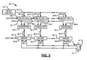
- an output port circuit 40is shown.
- the output port circuit 40is connected to the bias resistor 18 by the communication cable 14 .
- An output port 42provides an output signal having a predetermined slew rate.
- a delay setting module 43programmably sets slew rate by applying a delay signal to a delay time input 44 .
- the delay setting module 43may program all of the delay modules individually to two or more delay values and/or collectively to a common delay value. 1 to N conductors may be used to connect the delay setting module to the delay to the delay cells 46 .
- Cascaded delay cells 46 - 1 , 46 - 2 , . . . , 46 -N, referred to collectively as the cascaded delay cells 46each receive the delay signal.
- Each of the cascaded delay cells 46has an input 48 - 1 , 48 - 2 , . . . , 48 -N, referred to collectively as the data inputs 48 , that receive a data bit.
- Each of the cascaded delay cells 46also has a delayed data output 50 - 1 , 50 - 2 , . . . , 50 -N, referred to collectively as the delayed data outputs 50 .
- Each of the data inputs 48 - 2 through 48 -Nis connected to a delayed data output 50 - 1 , 50 - 2 , 50 -(N ⁇ 1) of the preceding cascaded delay cell 46 .
- the data input 48 - 1 of the first cascaded delay cell 46 - 1receives a data bit from an associated computing device 12 .
- Each cascaded delay cell 46propagates its data bit from its input 48 to its delayed data output 50 after the delay time. Therefore, the data bit applied to the first input 48 - 1 propagates to the last delayed data output 50 -N after N multiples of the delay time.
- N8 and each cascaded delay cell 46 provides a delay time between about 125 picoseconds and 375 picoseconds. The preferred embodiment thereby provides a slew rate adjustable between about 1 nanosecond and 3 nanoseconds, although other delay ranges can be used.
- An output enable line 52is active high and connected to a plurality of predrivers 54 - 1 , 54 - 2 , . . . , 54 -N, referred to collectively as the predrivers 54 .
- Each of the predrivers 54has a data input connected to the delayed data output 50 of a respective one of the cascaded delay cells 46 .
- Each of the predrivers 54implements a truth table, described later herein.
- the truth tableuses the output enable line 52 and the delayed data output 50 to generate four output signals.
- the four output signalsare communicated over output lines 56 - 1 , 56 - 2 , . . . , 56 -N, referred to collectively as output lines 56 , of each respective predriver 54 .
- each predriver 54is connected to a respective driver 58 - 1 , 58 - 2 , . . . , 58 -N, referred to collectively as the drivers 58 .
- Each of the drivers 58has an input for a reference current signal 60 and a driver output port 62 .
- the driver output ports 62are connected in parallel to form the output port 42 .
- the output enable line 52is high, a data bit propagates through the cascaded delay cells 46 and causes the driver output ports 62 to turn on or off in succession.
- a magnitude of a signal appearing at the output port 42increases or decreases, respectively, thereby providing a predetermined slew rate.
- FIG. 4a partial schematic diagram is shown of the output port circuit 40 .
- the three lines of delay time input 44are shown individually as 44 - 1 , 44 - 2 , and 44 - 3 .
- the delay time input 44is connected to a digital-to-analog converter (current DAC) 63 .
- a current output of the DAC 63is applied to a bias voltage generator 64 .
- the DAC 63receives the delay signal and converts it to a current as is described later.
- the bias voltage generator 64converts the current to a positive bias voltage 66 and a negative bias voltage 68 .
- the positive and negative bias voltages 66 , 68are applied to each of the cascaded delay cells 46 .
- the cascaded delay cells 46use the positive and negative bias voltages 66 , 68 to operate internal circuitry as described later.
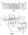
- the four output signals 56 from the predriver 54are connected to an H-bridge.
- An output signal PPis connected to a gate of a PFET Q 5 .
- An output signal NPis connected to a gate of an NFET Q 6 .
- An output signal NNis connected to a gate of an NFET Q 7 .
- An output signal PNis connected to a gate of a PFET Q 8 .
- a source of the NFET Q 6is connected to a source of the NFET Q 7 .
- a source of the PFET Q 5is connected to a source of PFET Q 8 .
- a drain of the NFET Q 6is connected to a drain of the PFET Q 5 and provides a negative node of the driver output port 62 .
- a drain of the NFET Q 7is connected to a drain of the PFET Q 8 and provides a positive node of the driver output port 62 .
- An NFET Q 9is configured as a current mirror and has a drain connected to the sources of the NFETs Q 6 and Q 7 .
- a PFET Q 10is configured as a current mirror and has a drain connected to the sources of the PFETs Q 5 and Q 8 .
- a current sourceis formed from NFETs Q 11 , Q 12 , and a PFET Q 13 .
- a gate and a drain of the NFET Q 11are connected to the reference current source 60 and a gate of the NFET Q 12 .
- a source of the NFET Q 11is connected to a source of the NFET Q 12 .
- a drain of the NFET Q 12is connected to a drain and a gate of the PFET Q 13 .
- the sources of the NFETs Q 11 and Q 12are connected to a source of each NFET Q 9 in the drivers 58 .
- a source of the PFET Q 13is connected to a source of each PFET Q 10 in the drivers 58 .
- the NFET Q 12 and the PFET Q 13mirror the reference current signal 60 flowing through the NFET Q 11 and provide current to the drivers 58 .
- the NFET Q 9 and PFET Q 10assure that the driver circuit output has a predetermined source impedance substantially free from influences resulting from process variations in manufacturing the NFETs and PFETs.
- the truth table 70has a first input column for the delayed data bit appearing at the delayed data output 50 .
- a second input columnis has a state of the output enable (OE) line 52 .
- OEoutput enable
- Four predriver output columnsare provided, one for each of the predriver output signals PP, NN, PN, and NP. Entries in the four columns parenthetically indicate whether the associated PFET or NFET Q 5 -Q 8 is turned on or turned off.
- a rightmost output columnindicates a logic state appearing at the driver output port 62 .
- the OE line 52is a active high signal.
- the PFETs and NFETs Q 5 -Q 8are turned off and the driver output port 62 is electrically open (3-state).
- the OE line 52is high and the delayed data bit is low, or logical 0, the PFET Q 5 and the NFET Q 7 are turned off, and the PFET Q 8 and the NFET Q 6 are turned on. This combination results in a logical 0 appearing at the driver output port 62 .
- the OE signalis high and the delayed data bit is high, or logical 1
- the PFET Q 5 and the NFET Q 7are turned on, and the PFET Q 8 and the NFET Q 6 are turned off. This combination results in a logical 1 appearing at the driver output port 62 .
- Conventional combinatorial logicmay be used to implement the truth table 70 in each of the predrivers 54 .
- the current DAC 63has an operational transconductance amplifier (OTA) with an output connected to gates of PFETs Q 14 , Q 15 , Q 16 , Q 17 , and Q 18 .
- An inverting input 74 of the OTA 72is connected to a constant voltage source VREF.
- a non-inverting input 76 of the OTA 72is connected to a drain of the PFET Q 14 and to one end of a resistor 65 . The other end of the resistor 65 is connected to the reference voltage VSS.
- the output of the OTA 72provides a current proportional to a voltage difference across the non-inverting 74 and inverting 76 inputs.
- a drain of the PFET Q 15is connected to the supply voltage VDD and to the drains of the PFETs Q 15 , Q 16 , and Q 18 .
- the three lines of the delay time input 44are connected to gates of PFETs Q 19 , Q 20 , and Q 21 , respectively.
- a source of the PFET Q 19is connected to a drain of the PFET Q 15 .
- a source of the PFET Q 20is connected to a drain of the PFET Q 16 .
- a source of the PFET Q 21is connected to a drain of the PFET Q 17 . Drains of the PFETs Q 18 -Q 21 are connected together and provide a programmable current output 78 .
- the PFET Q 14mirrors a current provided by the output of the OTA 72 .
- a magnitude of the currentis established by adjusting a resistance of the resistor 65 .
- the PFET Q 19is turned on by the first delay time input line 44 - 1
- the PFET Q 15mirrors the current flowing through the PFET Q 14 .
- the PFET Q 20is turned on by the second delay time input line 44 - 2
- the PFET Q 16mirrors the current flowing through the PFET Q 14 .
- the PFET Q 21is turned on by the third delay time input line 44 - 3
- the PFET Q 17mirrors the current flowing through the PFET Q 14 .
- PFETs Q 19 -Q 21being turned on by the delay time input lines 44
- an increasing current flowis established through the programmable current output 78 .
- the sizes of PFETs Q 15 -Q 18can be unequal to provide up to eight discrete levels of current flow through the programmable current output 78 in accordance with delay time input lines 44 turning on/off the PFETs Q 19 , Q 20 , and Q 21 .
- the current flow from the programmable current output 78is applied to a drain and a gate of an NFET Q 22 .
- a source of the NFET Q 22is connected to the reference voltage VSS, a source of an NFET Q 23 , and a source of an NFET Q 24 .
- a drain of the NFET Q 23is connected to a drain and a gate of a PFET Q 25 .
- a source of the PFET Q 25is connected to the voltage source VDD.
- a drain and a gate of the NFET Q 24are connected to a drain of a PFET Q 26 .
- a gate of the PFET Q 26is connected to the gate and the drain of the PFET Q 25 .
- a source of the PFET Q 26is connected to the supply voltage VDD.
- the drain of the PFET Q 25provides the positive bias voltage 66
- the drain of the NFET Q 24provides the negative bias voltage 68 .
- the current flow from the programmable current output 78is mirrored by the NFET Q 22 .
- the NFET Q 23mirrors the current flowing through the NFET Q 22 .
- the PFET Q 25drops a voltage across its source and drain as it mirrors the current flowing through the NFET Q 23 .
- the drain of the PFET Q 25thereby provides the positive voltage 66 with VDD less the voltage dropped across PFET Q 25 .
- the PFET Q 26mirrors the current flowing through the PFET Q 25 .
- the NFET Q 24drops a voltage across its source and drain as it mirrors the current flowing through the PFET Q 26 .
- the drain of the NFET Q 24thereby provides the negative voltage 68 with a voltage equal to its source-drain voltage drop.
- the positive 66 and negative 68 bias voltagesare applied to the delay cells 46 .
- FIG. 7a schematic diagram of a delay cell 46 is shown.
- a source of a PFET Q 27is connected to the supply voltage VDD.
- a gate of the PFET Q 27is connected to the positive bias voltage 66 .
- a drain of the PFET Q 27is connected to a source of a PFET Q 28 .
- a gate of the PFET Q 28is connected to the data bit input 48 of the delay cell 46 .
- a drain of the PFET Q 28is connected to a drain of an NFET Q 29 , to one end of a capacitor C 1 , and to an input of an inverter 80 .
- the other end of the capacitor C 1is connected to the reference voltage VSS.
- a source of the NFET Q 29is connected to a drain of an NFET Q 30 .
- a gate of the NFET Q 29is connected to the data bit input 48 of the delay cell 46 .
- a source of the NFET Q 30is connected to the reference voltage VSS.
- a gate of the NFET Q 30is connected to the negative bias voltage 68 .
- An output of the inverter 80provides the delayed data output 50 .
- a magnitude of the positive 66 and negative 68 bias voltagesestablishes drain-source resistances of the PFET Q 27 and the NFET Q 30 . If a logical 1 is applied to the data bit input 48 , the PFET Q 28 turns off and the NFET Q 29 turns on, thereby allowing the capacitor C 1 to discharge through the NFETs Q 29 and Q 30 .
- a rate of dischargeis determined by the magnitude of the negative bias voltage 68 . With the capacitor C 1 discharged, a logical 0 appears at the input of the inverter 80 and a logical 1 appears at the output of the inverter 80 . The rate of discharge determines the delay time for the delay cell 46 .
- a logical 0is applied to the data bit input 48 , the NFET Q 29 turns off and the PFET Q 28 turns on, thereby allowing the capacitor C 1 to charge through the PFETs Q 27 and Q 28 .
- a rate of chargeis determined by the magnitude of the positive bias voltage 66 .
- the rate of chargeis preferably equal to the rate of discharge.
- a horizontal axis of each plotindicates time in nanoseconds and a vertical axis of each plot represents volts.
- the column of plots at a left side of FIG. 8shows waveforms for a rising edge at the output port 42 caused by a logical 1 being applied to the data input 48 - 1 while the OE input 52 is high.
- a plot 82shows a set of time correlated curves 84 representing the output signals NN from the predrivers 54 .
- Each output signal NNbegins rising after its associated cascaded delay cell 46 propagates the logical 1 data bit.
- a plot 86shows a set of time correlated curves 88 representing the output signals PP from the predrivers 54 .
- Each output signal PPbegins falling after its associated cascaded delay cell 46 propagates the logical 1 data bit.
- a plot 90shows a set of time correlated curves 92 representing the output signals NP from the predrivers 54 .
- Each output signal NPbegins falling after its associated cascaded delay cell 46 propagates the logical 1 data bit.
- a plot 94shows a set of time correlated curves 96 representing the output signals PN from the predrivers 54 .
- Each output signal PNbegins rising after its associated cascaded delay cell 46 propagates the logical 1 data bit.
- a plot 98shows a signal voltage 100 rising at a controlled slew rate in unison with each driver output port 62 applying the logical 1 date bit to the output port 42 .
- the signal voltage 100rises as the drivers 58 activate in succession according to the output signals NN, PP, NP, and PN.
- the column of plots at a right side of FIG. 8shows waveforms for a falling edge at the output port 42 caused by a logical 0 being applied to the data input 48 - 1 while the OE input 52 is high.
- a plot 102shows a set of time correlated curves 104 representing the output signals NN from the predrivers 54 .
- Each output signal NNbegins falling after its associated cascaded delay cell 46 propagates the logical 0 data bit.
- a plot 106shows a set of time correlated curves 108 representing the output signals PP from the predrivers 54 .
- Each output signal PPbegins rising after its associated cascaded delay cell 46 propagates the logical 0 data bit.
- a plot 110shows a set of time correlated curves 112 representing the output signals NP from the predrivers 54 .
- Each output signal NPbegins rising after its associated cascaded delay cell 46 propagates the logical 0 data bit.
- a plot 114shows a set of time correlated curves 116 representing the output signals PN from the predrivers 54 .
- Each output signal PNbegins falling after its associated cascaded delay cell 46 propagates the logical 0 data bit.
- a plot 118shows a signal voltage 120 falling at a controlled slew rate in unison with each driver output port 62 applying the logical 0 data bit to the output port 42 .
- the signal voltage 120falls as the drivers 58 activate in succession according to the output signals NN, PP, NP, and PN.
- a time between each successive rising edge and/or each successive falling edge in the families of curvesis equal to the delay time of the cascaded delay cells 46 .
- Each of the cascaded delay cells 46provide the delay time in accordance with the delay time signal 44 .
- a horizontal axis of each plotindicates time in nanoseconds and a vertical axis of each plot represents volts.
- a plot 122shows a family of eight rising edge waveforms 124 . Each rising edge waveform is generated at the output port 42 with the cascaded delay cells 46 using a different one of eight discrete delay times. It can be seen from the family of rising edge waveforms 124 that increasing the delay time decreases the slew rate of the output port 42 .
- a plot 126shows a family of eight falling edge waveforms 128 .
- Each falling edge waveformis generated at the output port 42 with the cascaded delay cells using a different one of the eight discrete delay times. It can be seen from the family of rising edge waveforms 124 that decreasing the delay time increases the slew rate of the output port.
Landscapes
- Physics & Mathematics (AREA)
- Nonlinear Science (AREA)
- Logic Circuits (AREA)
Abstract
Description
Claims (40)
Priority Applications (3)
| Application Number | Priority Date | Filing Date | Title |
|---|---|---|---|
| US11/122,444US7298173B1 (en) | 2004-10-26 | 2005-05-05 | Slew rate control circuit for small computer system interface (SCSI) differential driver |
| US11/985,706US7579873B1 (en) | 2004-10-26 | 2007-11-16 | Slew rate control circuit for small computer system interface (SCSI) differential driver |
| US12/546,237US7719314B1 (en) | 2004-10-26 | 2009-08-24 | Slew rate control circuit for small computer system interface (SCSI) differential driver |
Applications Claiming Priority (2)
| Application Number | Priority Date | Filing Date | Title |
|---|---|---|---|
| US62219504P | 2004-10-26 | 2004-10-26 | |
| US11/122,444US7298173B1 (en) | 2004-10-26 | 2005-05-05 | Slew rate control circuit for small computer system interface (SCSI) differential driver |
Related Child Applications (1)
| Application Number | Title | Priority Date | Filing Date |
|---|---|---|---|
| US11/985,706ContinuationUS7579873B1 (en) | 2004-10-26 | 2007-11-16 | Slew rate control circuit for small computer system interface (SCSI) differential driver |
Publications (1)
| Publication Number | Publication Date |
|---|---|
| US7298173B1true US7298173B1 (en) | 2007-11-20 |
Family
ID=38690926
Family Applications (3)
| Application Number | Title | Priority Date | Filing Date |
|---|---|---|---|
| US11/122,444Expired - Fee RelatedUS7298173B1 (en) | 2004-10-26 | 2005-05-05 | Slew rate control circuit for small computer system interface (SCSI) differential driver |
| US11/985,706Expired - LifetimeUS7579873B1 (en) | 2004-10-26 | 2007-11-16 | Slew rate control circuit for small computer system interface (SCSI) differential driver |
| US12/546,237Expired - LifetimeUS7719314B1 (en) | 2004-10-26 | 2009-08-24 | Slew rate control circuit for small computer system interface (SCSI) differential driver |
Family Applications After (2)
| Application Number | Title | Priority Date | Filing Date |
|---|---|---|---|
| US11/985,706Expired - LifetimeUS7579873B1 (en) | 2004-10-26 | 2007-11-16 | Slew rate control circuit for small computer system interface (SCSI) differential driver |
| US12/546,237Expired - LifetimeUS7719314B1 (en) | 2004-10-26 | 2009-08-24 | Slew rate control circuit for small computer system interface (SCSI) differential driver |
Country Status (1)
| Country | Link |
|---|---|
| US (3) | US7298173B1 (en) |
Cited By (19)
| Publication number | Priority date | Publication date | Assignee | Title |
|---|---|---|---|---|
| US20080297210A1 (en)* | 2006-08-21 | 2008-12-04 | Woo-Seok Kim | Clock multiplier and clock generator having the same |
| US20100052735A1 (en)* | 2008-08-28 | 2010-03-04 | Micrel, Incorporated | Slew rate controlled level shifter with reduced quiescent current |
| US7719314B1 (en) | 2004-10-26 | 2010-05-18 | Marvell International Ltd. | Slew rate control circuit for small computer system interface (SCSI) differential driver |
| US20100238848A1 (en)* | 2005-08-19 | 2010-09-23 | National Semiconductor Corporation | Class-B transmitter and replica transmitter for gigabit ethernet applications |
| US20100283507A1 (en)* | 2009-05-07 | 2010-11-11 | Faraday Technology Corp. | Current source applicable to a controllable delay line and design method thereof |
| US20110057692A1 (en)* | 2007-08-17 | 2011-03-10 | Raytheon Company | Digital circuits with adaptive resistance to single event upset |
| US7928784B2 (en) | 2009-06-26 | 2011-04-19 | Texas Instruments Incorporated | Method and apparatus to improve and control the propagation delay in a current slewing circuit |
| US20110234317A1 (en)* | 2009-10-14 | 2011-09-29 | Advantest Corporation | Differential driver circuit |
| CN103633987A (en)* | 2012-08-20 | 2014-03-12 | 爱思开海力士有限公司 | Signal transmission circuits |
| US20150022243A1 (en)* | 2013-07-16 | 2015-01-22 | Mediatek Inc. | Driver circuit for signal transmission and control method of driver circuit |
| US20160197598A1 (en)* | 2013-07-16 | 2016-07-07 | Mediatek Inc. | Driver circuit for signal transmission and control method of driver circuit |
| US9590610B2 (en) | 2014-12-30 | 2017-03-07 | Mediatek Inc. | Driver circuit for signal transmission and control method of driver circuit |
| US9590595B2 (en) | 2015-01-08 | 2017-03-07 | Mediatek Inc. | Driver circuit with feed-forward equalizer |
| CN106961270A (en)* | 2016-01-12 | 2017-07-18 | 综合器件技术公司 | Signal driver slew-rate control |
| US10700685B1 (en)* | 2019-01-17 | 2020-06-30 | Shanghai Zhaoxin Semiconductor Co., Ltd. | High-speed signal driving device |
| US10826268B1 (en) | 2019-06-27 | 2020-11-03 | Stmicroelectronics S.R.L. | Laser driver incorporating clamping circuit with freewheeling diode |
| CN112152597A (en)* | 2019-06-27 | 2020-12-29 | 意法半导体股份有限公司 | PVT Compensated Delay Cell for Monostable |
| US11128284B2 (en) | 2019-09-12 | 2021-09-21 | Ali Corporation | Control circuit for controlling signal rising time and falling time |
| US11387625B2 (en) | 2019-06-27 | 2022-07-12 | Stmicroelectronics S.R.L. | Pulse width check circuit for laser diode pulse generator |
Families Citing this family (6)
| Publication number | Priority date | Publication date | Assignee | Title |
|---|---|---|---|---|
| JPWO2010095378A1 (en)* | 2009-02-18 | 2012-08-23 | 株式会社アドバンテスト | Output device and test device |
| US8022730B2 (en)* | 2009-10-13 | 2011-09-20 | Himax Technologies Limited | Driving circuit with slew-rate enhancement circuit |
| JP5743063B2 (en)* | 2011-02-09 | 2015-07-01 | ラピスセミコンダクタ株式会社 | Semiconductor integrated circuit, semiconductor chip, and semiconductor integrated circuit design method |
| KR101924860B1 (en)* | 2012-06-29 | 2018-12-05 | 에스케이하이닉스 주식회사 | Signal transmission circuit |
| KR102021336B1 (en)* | 2012-12-20 | 2019-09-16 | 에스케이하이닉스 주식회사 | Semiconductor device and operating methode for the same |
| CN118157692A (en)* | 2022-12-07 | 2024-06-07 | 微芯片技术股份有限公司 | Reducing emissions at predetermined frequencies using delay elements and related devices, methods, and systems |
Citations (95)
| Publication number | Priority date | Publication date | Assignee | Title |
|---|---|---|---|---|
| US3543009A (en) | 1966-05-13 | 1970-11-24 | Research Corp | Binary transversal filter systems |
| US4112253A (en) | 1976-07-22 | 1978-09-05 | Siemens Aktiengesellschaft | Device for the transmission of push-pull signals across a two-wire line in full duplex operation |
| US4131767A (en) | 1976-09-07 | 1978-12-26 | Bell Telephone Laboratories, Incorporated | Echo cancellation in two-wire, two-way data transmission systems |
| US4152541A (en) | 1978-02-03 | 1979-05-01 | Burroughs Corporation | Full duplex driver/receiver |
| USRE30111E (en) | 1974-10-15 | 1979-10-09 | Motorola, Inc. | Digital single signal line full duplex method and apparatus |
| US4362909A (en) | 1979-05-14 | 1982-12-07 | U.S. Philips Corporation | Echo canceler with high-pass filter |
| JPS58111415A (en) | 1981-12-24 | 1983-07-02 | Fujitsu Ltd | Offset cancelling circuit for differential amplifier |
| US4393494A (en) | 1979-10-04 | 1983-07-12 | Cselt Centro Studi E Laboratori Telecomunicazioni S.P.A. | Transceiver for full-duplex transmission of digital signals over a common line |
| US4727566A (en) | 1984-02-01 | 1988-02-23 | Telefonaktiebolaget Lm Ericsson | Method to test the function of an adaptive echo canceller |
| US4888762A (en) | 1987-02-17 | 1989-12-19 | Nec Corporation | Echo canceller for bidirectional transmission on two-wire subscriber lines |
| US4935919A (en) | 1986-09-16 | 1990-06-19 | Nec Corporation | Full duplex modem having two echo cancellers for a near end echo and a far end echo |
| US4947171A (en) | 1988-03-31 | 1990-08-07 | Deutsche Itt Industries Gmbh | Circuit arrangement for averaging signals during pulse-density D/A or A/D conversion |
| US4999830A (en) | 1989-09-25 | 1991-03-12 | At&T Bell Laboratories | Communication system analog-to-digital converter using echo information to improve resolution |
| JPH03273704A (en) | 1990-03-22 | 1991-12-04 | Mitsubishi Electric Corp | Amplifier |
| JPH04293306A (en) | 1991-03-22 | 1992-10-16 | Mitsubishi Electric Corp | Amplifier |
| JPH04351109A (en) | 1991-05-29 | 1992-12-04 | Nec Corp | Composite differential amplifier |
| US5222084A (en) | 1990-06-25 | 1993-06-22 | Nec Corporation | Echo canceler having adaptive digital filter unit associated with delta-sigma modulation circuit |
| US5305379A (en) | 1991-05-22 | 1994-04-19 | Hitachi, Ltd. | Semiconductor integrated device |
| US5307405A (en) | 1992-09-25 | 1994-04-26 | Qualcomm Incorporated | Network echo canceller |
| US5323157A (en) | 1993-01-15 | 1994-06-21 | Motorola, Inc. | Sigma-delta digital-to-analog converter with reduced noise |
| US5357145A (en) | 1992-12-22 | 1994-10-18 | National Semiconductor Corporation | Integrated waveshaping circuit using weighted current summing |
| US5388092A (en) | 1989-06-27 | 1995-02-07 | Nec Corporation | Echo canceller for two-wire full duplex digital data transmission |
| JPH07131260A (en) | 1993-11-05 | 1995-05-19 | Hitachi Ltd | Semiconductor integrated circuit |
| US5418478A (en) | 1993-07-30 | 1995-05-23 | Apple Computer, Inc. | CMOS differential twisted-pair driver |
| US5465272A (en) | 1994-04-08 | 1995-11-07 | Synoptics Communications, Inc. | Data transmitter baseline wander correction circuit |
| US5471665A (en) | 1994-10-18 | 1995-11-28 | Motorola, Inc. | Differential DC offset compensation circuit |
| US5489873A (en) | 1994-03-03 | 1996-02-06 | Motorola, Inc. | Active low-pass filter |
| US5508656A (en) | 1993-12-23 | 1996-04-16 | Sgs-Thomson Microelectronics S.A. | Amplifier with offset correction |
| US5517141A (en) | 1993-11-05 | 1996-05-14 | Motorola, Inc. | Differential high speed track and hold amplifier |
| US5517435A (en) | 1993-03-11 | 1996-05-14 | Nec Corporation | Method of identifying an unknown system with a band-splitting adaptive filter and a device thereof |
| US5539773A (en) | 1992-02-17 | 1996-07-23 | Thomson Consumer Electronics S.A. | Method and apparatus for ghost cancelling and/or equalizing |
| US5572158A (en) | 1994-02-15 | 1996-11-05 | Rambus, Inc. | Amplifier with active duty cycle correction |
| US5587681A (en) | 1993-10-29 | 1996-12-24 | Plessey Semiconductors Limited | DC restoration circuit |
| US5596439A (en) | 1995-08-01 | 1997-01-21 | Viasat, Inc. | Self-interference cancellation for two-party relayed communication |
| US5625357A (en) | 1995-02-16 | 1997-04-29 | Advanced Micro Devices, Inc. | Current steering semi-digital reconstruction filter |
| US5648738A (en) | 1994-11-01 | 1997-07-15 | Cirrus Logic, Inc. | Read channel having auto-zeroing and offset compensation, and power-down between servo fields |
| US5651029A (en) | 1995-05-16 | 1997-07-22 | Myson Technology, Inc. | Apparatus for transmitting an output with predetermined frequency response to an unshielded twisted-pair media and waveform shaping circuit and method employed therein |
| US5659609A (en) | 1994-09-05 | 1997-08-19 | Fujitsu Limited | Echo canceller and waveform-distortion compensation device |
| US5663728A (en) | 1995-05-18 | 1997-09-02 | Hughes Aircraft Company | Digital-to-analog converted (DAC) and method that set waveform rise and fall times to produce an analog waveform that approximates a piecewise linear waveform to reduce spectral distortion |
| US5666354A (en) | 1995-12-20 | 1997-09-09 | International Business Machines Corporation | CMOS bi-directional differential link |
| EP0800278A1 (en) | 1996-04-04 | 1997-10-08 | Plessey Semiconductors Limited | An error correction circuit |
| JPH10126183A (en) | 1996-10-21 | 1998-05-15 | Oki Electric Ind Co Ltd | Differential amplifier and limiter amplifier |
| US5757219A (en) | 1996-01-31 | 1998-05-26 | Analogic Corporation | Apparatus for and method of autozeroing the input of a charge-to-voltage converter |
| US5796725A (en) | 1994-08-31 | 1998-08-18 | Nec Corporation | Echo canceller capable of cancelling an echo signal at a high speed |
| US5798664A (en) | 1995-04-07 | 1998-08-25 | Nec Corporation | Offset cancelling amplifier circuit having Miller integrator as offset detector |
| US5822426A (en) | 1995-06-06 | 1998-10-13 | International Business Machines Corporation | Balanced hybrid circuit |
| US5825819A (en) | 1996-04-23 | 1998-10-20 | Motorola, Inc. | Asymmetrical digital subscriber line (ADSL) line driver circuit |
| US5844439A (en) | 1996-03-13 | 1998-12-01 | Integrated Circuit Systems, Inc. | DC restoration circuit for multi-level transmission signals |
| US5864587A (en) | 1995-06-06 | 1999-01-26 | Lsi Logic Corporation | Differential signal receiver |
| US5880615A (en) | 1996-12-10 | 1999-03-09 | Intel Corporation | Method and apparatus for detecting differential threshold levels while compensating for baseline wander |
| US5936450A (en) | 1997-03-21 | 1999-08-10 | National Semiconductor Corporation | Waveshaping circuit using digitally controlled weighted current summing |
| US5940498A (en) | 1996-06-14 | 1999-08-17 | Siemens Aktiengesellschaft | Electronic voice circuit configuration |
| US5940442A (en) | 1997-01-30 | 1999-08-17 | National Semioonductor Corporation | High speed data receiver |
| WO1999046867A1 (en) | 1998-03-09 | 1999-09-16 | Broadcom Corporation | Gigabit ethernet transceiver |
| US6043766A (en) | 1997-12-10 | 2000-03-28 | National Semiconductor Corporation | Distributive encoder for encoding error signals which represent signal peak errors in data signals for identifying erroneous signal baseline, peak and equalization conditions |
| US6044489A (en) | 1997-12-10 | 2000-03-28 | National Semiconductor Corporation | Data signal baseline error detector |
| WO2000027079A1 (en) | 1998-10-30 | 2000-05-11 | Broadcom Corporation | Internet gigabit ethernet transmitter architecture |
| WO2000028668A1 (en) | 1998-11-09 | 2000-05-18 | Broadcom Corporation | Forward error corrector |
| US6067327A (en) | 1997-09-18 | 2000-05-23 | International Business Machines Corporation | Data transmitter and method therefor |
| WO2000035094A1 (en) | 1998-12-07 | 2000-06-15 | Broadcom Corporation | Low jitter high phase resolution pll-based timing recovery system |
| WO2000028663A3 (en) | 1998-11-09 | 2000-08-17 | Broadcom Corp | Fir filter structure with low latency for gigabit ethernet applications |
| US6121831A (en) | 1999-05-12 | 2000-09-19 | Level One Communications, Inc. | Apparatus and method for removing offset in a gain circuit |
| US6140857A (en) | 1999-03-29 | 2000-10-31 | Intel Corporation | Method and apparatus for reducing baseline wander |
| US6148025A (en) | 1998-04-17 | 2000-11-14 | Lucent Technologies, Inc. | System and method for compensating for baseline wander |
| WO2000028691A3 (en) | 1998-11-09 | 2000-11-23 | Broadcom Corp | Multi-pair gigabit ethernet transceiver |
| US6172634B1 (en) | 1998-02-25 | 2001-01-09 | Lucent Technologies Inc. | Methods and apparatus for providing analog-fir-based line-driver with pre-equalization |
| US6185263B1 (en) | 1998-11-09 | 2001-02-06 | Broadcom Corporation | Adaptively configurable class-A/class-B transmit DAC for transceiver emission and power consumption control |
| US6188282B1 (en) | 1999-10-08 | 2001-02-13 | Ericsson Inc. | Differential amplifier with reduced even order non-linearity and associated methods |
| US6249164B1 (en) | 1998-09-25 | 2001-06-19 | International Business Machines Corporation | Delay circuit arrangement for use in a DAC/driver waveform generator with phase lock rise time control |
| US6259680B1 (en) | 1997-10-01 | 2001-07-10 | Adtran, Inc. | Method and apparatus for echo cancellation |
| US6275098B1 (en) | 1999-10-01 | 2001-08-14 | Lsi Logic Corporation | Digitally calibrated bandgap reference |
| US6288604B1 (en) | 1998-02-03 | 2001-09-11 | Broadcom Corporation | CMOS amplifier providing automatic offset cancellation |
| US20010050585A1 (en) | 2000-01-18 | 2001-12-13 | Larrie Carr | Digital delay line with synchronous control |
| WO2000028712A9 (en) | 1998-10-30 | 2001-12-20 | Broadcom Corp | Cable modem system |
| USRE37619E1 (en) | 1996-01-05 | 2002-04-02 | Analog Devices, Inc. | Skewless differential switch and DAC employing the same |
| US6373908B2 (en) | 1998-11-11 | 2002-04-16 | Broadcom Corporation | Adaptive electronic transmission signal cancellation apparatus for full duplex communication |
| TW497334B (en) | 2000-09-15 | 2002-08-01 | Realtek Semiconductor Co Ltd | Device and method for correcting baseline wandering |
| US6433608B1 (en) | 2001-01-02 | 2002-08-13 | Realtek Semi-Conductor Co., Ltd. | Device and method for correcting the baseline wandering of transmitting signals |
| US20020136321A1 (en) | 1998-10-30 | 2002-09-26 | Chan Kevin T. | Reduction of aggregate EMI emissions of multiple transmitters |
| US6462688B1 (en) | 2000-12-18 | 2002-10-08 | Marvell International, Ltd. | Direct drive programmable high speed power digital-to-analog converter |
| US6477200B1 (en) | 1998-11-09 | 2002-11-05 | Broadcom Corporation | Multi-pair gigabit ethernet transceiver |
| TW512608B (en) | 2001-02-13 | 2002-12-01 | Realtek Semi Conductor Corp | Receiver and method for receiving fast ethernet data without baseline wander effect |
| US20020181601A1 (en) | 2001-03-21 | 2002-12-05 | Chin-Wen Huang | Receiver with baseline wander correction and correction method thereof |
| US6509857B1 (en) | 1999-10-25 | 2003-01-21 | Texas Instruments Incorporated | Digital-to-analog converting method and digital-to-analog converter |
| US6570931B1 (en) | 1999-12-31 | 2003-05-27 | Intel Corporation | Switched voltage adaptive slew rate control and spectrum shaping transmitter for high speed digital transmission |
| US6597233B2 (en) | 2001-05-25 | 2003-07-22 | International Business Machines Corporation | Differential SCSI driver rise time and amplitude control circuit |
| US20040005015A1 (en) | 1998-10-30 | 2004-01-08 | Chan Kevin T. | Method and system for a reduced emissions direct drive transmitter for unshielded twisted pair (UTP) applications |
| US6687286B1 (en) | 1999-12-17 | 2004-02-03 | Agere Systems, Inc. | Programmable transmitter circuit for coupling to an ethernet or fast ethernet |
| US6710617B2 (en)* | 2002-01-10 | 2004-03-23 | Agilent Technologies, Inc. | Variable slew rate control for open drain bus |
| US20040091071A1 (en) | 2002-11-07 | 2004-05-13 | Realtek Semiconductor Corp. | Demodulation apparatus for a network transceiver and method thereof |
| US20040090981A1 (en) | 2002-11-07 | 2004-05-13 | Realtek Semiconductor Corp. | Initialization method for a network system |
| US20040208312A1 (en) | 1997-09-16 | 2004-10-21 | Kozo Okuda | Echo canceling method, echo canceller, and voice switch |
| DE102004017497A1 (en) | 2003-04-14 | 2004-11-25 | Realtek Semiconductor Corp. | amplifier circuit |
| US6882216B2 (en) | 2003-06-24 | 2005-04-19 | Realtek Semiconductor Corp. | On-chip high-pass filter with large time constant |
| US20060038596A1 (en)* | 2004-08-18 | 2006-02-23 | Binan Wang | Delay locked loop circuitry and method for optimizing delay timing in mixed signal systems |
Family Cites Families (7)
| Publication number | Priority date | Publication date | Assignee | Title |
|---|---|---|---|---|
| US5066873A (en)* | 1989-12-04 | 1991-11-19 | Altera Corporation | Integrated circuits with reduced switching noise |
| JP3273704B2 (en) | 1994-11-09 | 2002-04-15 | 新日本製鐵株式会社 | Mold width change control method for continuous casting equipment |
| US5712884A (en)* | 1995-03-31 | 1998-01-27 | Samsung Electronics Co., Ltd. | Data receiving method and circuit of digital communication system |
| US6721114B1 (en)* | 2001-05-09 | 2004-04-13 | Marvell International, Ltd. | Precompensation circuit for magnetic recording |
| JP4293306B2 (en) | 2003-11-04 | 2009-07-08 | ナスニックス株式会社 | Attractor ties |
| JP4351109B2 (en) | 2004-04-12 | 2009-10-28 | 旭ファイバーグラス株式会社 | Inorganic fiber mat |
| US7298173B1 (en) | 2004-10-26 | 2007-11-20 | Marvell International Ltd. | Slew rate control circuit for small computer system interface (SCSI) differential driver |
- 2005
- 2005-05-05USUS11/122,444patent/US7298173B1/ennot_activeExpired - Fee Related
- 2007
- 2007-11-16USUS11/985,706patent/US7579873B1/ennot_activeExpired - Lifetime
- 2009
- 2009-08-24USUS12/546,237patent/US7719314B1/ennot_activeExpired - Lifetime
Patent Citations (106)
| Publication number | Priority date | Publication date | Assignee | Title |
|---|---|---|---|---|
| US3543009A (en) | 1966-05-13 | 1970-11-24 | Research Corp | Binary transversal filter systems |
| USRE30111E (en) | 1974-10-15 | 1979-10-09 | Motorola, Inc. | Digital single signal line full duplex method and apparatus |
| US4112253A (en) | 1976-07-22 | 1978-09-05 | Siemens Aktiengesellschaft | Device for the transmission of push-pull signals across a two-wire line in full duplex operation |
| US4131767A (en) | 1976-09-07 | 1978-12-26 | Bell Telephone Laboratories, Incorporated | Echo cancellation in two-wire, two-way data transmission systems |
| US4152541A (en) | 1978-02-03 | 1979-05-01 | Burroughs Corporation | Full duplex driver/receiver |
| US4362909A (en) | 1979-05-14 | 1982-12-07 | U.S. Philips Corporation | Echo canceler with high-pass filter |
| US4393494A (en) | 1979-10-04 | 1983-07-12 | Cselt Centro Studi E Laboratori Telecomunicazioni S.P.A. | Transceiver for full-duplex transmission of digital signals over a common line |
| JPS58111415A (en) | 1981-12-24 | 1983-07-02 | Fujitsu Ltd | Offset cancelling circuit for differential amplifier |
| US4727566A (en) | 1984-02-01 | 1988-02-23 | Telefonaktiebolaget Lm Ericsson | Method to test the function of an adaptive echo canceller |
| US4935919A (en) | 1986-09-16 | 1990-06-19 | Nec Corporation | Full duplex modem having two echo cancellers for a near end echo and a far end echo |
| US4888762A (en) | 1987-02-17 | 1989-12-19 | Nec Corporation | Echo canceller for bidirectional transmission on two-wire subscriber lines |
| US4947171A (en) | 1988-03-31 | 1990-08-07 | Deutsche Itt Industries Gmbh | Circuit arrangement for averaging signals during pulse-density D/A or A/D conversion |
| US5388092A (en) | 1989-06-27 | 1995-02-07 | Nec Corporation | Echo canceller for two-wire full duplex digital data transmission |
| US4999830A (en) | 1989-09-25 | 1991-03-12 | At&T Bell Laboratories | Communication system analog-to-digital converter using echo information to improve resolution |
| JPH03273704A (en) | 1990-03-22 | 1991-12-04 | Mitsubishi Electric Corp | Amplifier |
| US5222084A (en) | 1990-06-25 | 1993-06-22 | Nec Corporation | Echo canceler having adaptive digital filter unit associated with delta-sigma modulation circuit |
| JPH04293306A (en) | 1991-03-22 | 1992-10-16 | Mitsubishi Electric Corp | Amplifier |
| US5305379A (en) | 1991-05-22 | 1994-04-19 | Hitachi, Ltd. | Semiconductor integrated device |
| JPH04351109A (en) | 1991-05-29 | 1992-12-04 | Nec Corp | Composite differential amplifier |
| US5539773A (en) | 1992-02-17 | 1996-07-23 | Thomson Consumer Electronics S.A. | Method and apparatus for ghost cancelling and/or equalizing |
| US5307405A (en) | 1992-09-25 | 1994-04-26 | Qualcomm Incorporated | Network echo canceller |
| US5357145A (en) | 1992-12-22 | 1994-10-18 | National Semiconductor Corporation | Integrated waveshaping circuit using weighted current summing |
| US5323157A (en) | 1993-01-15 | 1994-06-21 | Motorola, Inc. | Sigma-delta digital-to-analog converter with reduced noise |
| US5517435A (en) | 1993-03-11 | 1996-05-14 | Nec Corporation | Method of identifying an unknown system with a band-splitting adaptive filter and a device thereof |
| US5418478A (en) | 1993-07-30 | 1995-05-23 | Apple Computer, Inc. | CMOS differential twisted-pair driver |
| US5587681A (en) | 1993-10-29 | 1996-12-24 | Plessey Semiconductors Limited | DC restoration circuit |
| JPH07131260A (en) | 1993-11-05 | 1995-05-19 | Hitachi Ltd | Semiconductor integrated circuit |
| US5517141A (en) | 1993-11-05 | 1996-05-14 | Motorola, Inc. | Differential high speed track and hold amplifier |
| US5508656A (en) | 1993-12-23 | 1996-04-16 | Sgs-Thomson Microelectronics S.A. | Amplifier with offset correction |
| US5572158A (en) | 1994-02-15 | 1996-11-05 | Rambus, Inc. | Amplifier with active duty cycle correction |
| US5489873A (en) | 1994-03-03 | 1996-02-06 | Motorola, Inc. | Active low-pass filter |
| US5465272A (en) | 1994-04-08 | 1995-11-07 | Synoptics Communications, Inc. | Data transmitter baseline wander correction circuit |
| US5796725A (en) | 1994-08-31 | 1998-08-18 | Nec Corporation | Echo canceller capable of cancelling an echo signal at a high speed |
| US5659609A (en) | 1994-09-05 | 1997-08-19 | Fujitsu Limited | Echo canceller and waveform-distortion compensation device |
| US5471665A (en) | 1994-10-18 | 1995-11-28 | Motorola, Inc. | Differential DC offset compensation circuit |
| US5648738A (en) | 1994-11-01 | 1997-07-15 | Cirrus Logic, Inc. | Read channel having auto-zeroing and offset compensation, and power-down between servo fields |
| US5625357A (en) | 1995-02-16 | 1997-04-29 | Advanced Micro Devices, Inc. | Current steering semi-digital reconstruction filter |
| US5798664A (en) | 1995-04-07 | 1998-08-25 | Nec Corporation | Offset cancelling amplifier circuit having Miller integrator as offset detector |
| US5651029A (en) | 1995-05-16 | 1997-07-22 | Myson Technology, Inc. | Apparatus for transmitting an output with predetermined frequency response to an unshielded twisted-pair media and waveform shaping circuit and method employed therein |
| US5663728A (en) | 1995-05-18 | 1997-09-02 | Hughes Aircraft Company | Digital-to-analog converted (DAC) and method that set waveform rise and fall times to produce an analog waveform that approximates a piecewise linear waveform to reduce spectral distortion |
| US5864587A (en) | 1995-06-06 | 1999-01-26 | Lsi Logic Corporation | Differential signal receiver |
| US5822426A (en) | 1995-06-06 | 1998-10-13 | International Business Machines Corporation | Balanced hybrid circuit |
| US5596439A (en) | 1995-08-01 | 1997-01-21 | Viasat, Inc. | Self-interference cancellation for two-party relayed communication |
| US5666354A (en) | 1995-12-20 | 1997-09-09 | International Business Machines Corporation | CMOS bi-directional differential link |
| USRE37619E1 (en) | 1996-01-05 | 2002-04-02 | Analog Devices, Inc. | Skewless differential switch and DAC employing the same |
| US5757219A (en) | 1996-01-31 | 1998-05-26 | Analogic Corporation | Apparatus for and method of autozeroing the input of a charge-to-voltage converter |
| US5844439A (en) | 1996-03-13 | 1998-12-01 | Integrated Circuit Systems, Inc. | DC restoration circuit for multi-level transmission signals |
| EP0800278A1 (en) | 1996-04-04 | 1997-10-08 | Plessey Semiconductors Limited | An error correction circuit |
| US5825819A (en) | 1996-04-23 | 1998-10-20 | Motorola, Inc. | Asymmetrical digital subscriber line (ADSL) line driver circuit |
| US5940498A (en) | 1996-06-14 | 1999-08-17 | Siemens Aktiengesellschaft | Electronic voice circuit configuration |
| JPH10126183A (en) | 1996-10-21 | 1998-05-15 | Oki Electric Ind Co Ltd | Differential amplifier and limiter amplifier |
| US5880615A (en) | 1996-12-10 | 1999-03-09 | Intel Corporation | Method and apparatus for detecting differential threshold levels while compensating for baseline wander |
| US5940442A (en) | 1997-01-30 | 1999-08-17 | National Semioonductor Corporation | High speed data receiver |
| US5936450A (en) | 1997-03-21 | 1999-08-10 | National Semiconductor Corporation | Waveshaping circuit using digitally controlled weighted current summing |
| US20040208312A1 (en) | 1997-09-16 | 2004-10-21 | Kozo Okuda | Echo canceling method, echo canceller, and voice switch |
| US6067327A (en) | 1997-09-18 | 2000-05-23 | International Business Machines Corporation | Data transmitter and method therefor |
| US6259680B1 (en) | 1997-10-01 | 2001-07-10 | Adtran, Inc. | Method and apparatus for echo cancellation |
| US6043766A (en) | 1997-12-10 | 2000-03-28 | National Semiconductor Corporation | Distributive encoder for encoding error signals which represent signal peak errors in data signals for identifying erroneous signal baseline, peak and equalization conditions |
| US6044489A (en) | 1997-12-10 | 2000-03-28 | National Semiconductor Corporation | Data signal baseline error detector |
| US6288604B1 (en) | 1998-02-03 | 2001-09-11 | Broadcom Corporation | CMOS amplifier providing automatic offset cancellation |
| US6172634B1 (en) | 1998-02-25 | 2001-01-09 | Lucent Technologies Inc. | Methods and apparatus for providing analog-fir-based line-driver with pre-equalization |
| WO1999046867A1 (en) | 1998-03-09 | 1999-09-16 | Broadcom Corporation | Gigabit ethernet transceiver |
| US6148025A (en) | 1998-04-17 | 2000-11-14 | Lucent Technologies, Inc. | System and method for compensating for baseline wander |
| US6249164B1 (en) | 1998-09-25 | 2001-06-19 | International Business Machines Corporation | Delay circuit arrangement for use in a DAC/driver waveform generator with phase lock rise time control |
| US6259745B1 (en) | 1998-10-30 | 2001-07-10 | Broadcom Corporation | Integrated Gigabit Ethernet transmitter architecture |
| US20040005015A1 (en) | 1998-10-30 | 2004-01-08 | Chan Kevin T. | Method and system for a reduced emissions direct drive transmitter for unshielded twisted pair (UTP) applications |
| US6690742B2 (en) | 1998-10-30 | 2004-02-10 | Broadcom Corporation | Adaptively configurable class-A/class-B transmit DAC for transceiver emission and power consumption control |
| US20020136321A1 (en) | 1998-10-30 | 2002-09-26 | Chan Kevin T. | Reduction of aggregate EMI emissions of multiple transmitters |
| US20030002570A1 (en) | 1998-10-30 | 2003-01-02 | Chan Kevin T. | Fully integrated ethernet transmitter architecture with interpolating filtering |
| US6594304B2 (en) | 1998-10-30 | 2003-07-15 | Broadcom Corporation | Adaptive configurable class-A/class-B transmit DAC for transceiver emission and power consumption control |
| US20040105504A1 (en) | 1998-10-30 | 2004-06-03 | Chan Kevin T. | Adaptively configurable class-A/class-B transmit DAC for transceiver emission and power consumption control |
| US6411647B1 (en) | 1998-10-30 | 2002-06-25 | Broadcom Corporation | Fully integrated ethernet transmitter architecture with interpolating filtering |
| WO2000027079A1 (en) | 1998-10-30 | 2000-05-11 | Broadcom Corporation | Internet gigabit ethernet transmitter architecture |
| US6389077B1 (en) | 1998-10-30 | 2002-05-14 | Broadcom Corporation | Adaptively configurable class-A/class-B transmit DAC for transceiver emission and power consumption control |
| US6332004B1 (en) | 1998-10-30 | 2001-12-18 | Broadcom Corporation | Analog discrete-time filtering for unshielded twisted pair data communication |
| WO2000028712A9 (en) | 1998-10-30 | 2001-12-20 | Broadcom Corp | Cable modem system |
| US6185263B1 (en) | 1998-11-09 | 2001-02-06 | Broadcom Corporation | Adaptively configurable class-A/class-B transmit DAC for transceiver emission and power consumption control |
| WO2000028668A1 (en) | 1998-11-09 | 2000-05-18 | Broadcom Corporation | Forward error corrector |
| WO2000028663A3 (en) | 1998-11-09 | 2000-08-17 | Broadcom Corp | Fir filter structure with low latency for gigabit ethernet applications |
| US6477200B1 (en) | 1998-11-09 | 2002-11-05 | Broadcom Corporation | Multi-pair gigabit ethernet transceiver |
| WO2000028691A3 (en) | 1998-11-09 | 2000-11-23 | Broadcom Corp | Multi-pair gigabit ethernet transceiver |
| US20050025266A1 (en) | 1998-11-11 | 2005-02-03 | Chan Kevin T. | Adaptive electronic transmission signal cancellation apparatus for full duplex communication |
| US6744831B2 (en) | 1998-11-11 | 2004-06-01 | Broadcom Corporation | Adaptive electronic transmission signal cancellation apparatus for full duplex communication |
| US6373908B2 (en) | 1998-11-11 | 2002-04-16 | Broadcom Corporation | Adaptive electronic transmission signal cancellation apparatus for full duplex communication |
| WO2000035094A1 (en) | 1998-12-07 | 2000-06-15 | Broadcom Corporation | Low jitter high phase resolution pll-based timing recovery system |
| US6140857A (en) | 1999-03-29 | 2000-10-31 | Intel Corporation | Method and apparatus for reducing baseline wander |
| US6121831A (en) | 1999-05-12 | 2000-09-19 | Level One Communications, Inc. | Apparatus and method for removing offset in a gain circuit |
| US6275098B1 (en) | 1999-10-01 | 2001-08-14 | Lsi Logic Corporation | Digitally calibrated bandgap reference |
| US6188282B1 (en) | 1999-10-08 | 2001-02-13 | Ericsson Inc. | Differential amplifier with reduced even order non-linearity and associated methods |
| US6509857B1 (en) | 1999-10-25 | 2003-01-21 | Texas Instruments Incorporated | Digital-to-analog converting method and digital-to-analog converter |
| US6687286B1 (en) | 1999-12-17 | 2004-02-03 | Agere Systems, Inc. | Programmable transmitter circuit for coupling to an ethernet or fast ethernet |
| US6570931B1 (en) | 1999-12-31 | 2003-05-27 | Intel Corporation | Switched voltage adaptive slew rate control and spectrum shaping transmitter for high speed digital transmission |
| US20010050585A1 (en) | 2000-01-18 | 2001-12-13 | Larrie Carr | Digital delay line with synchronous control |
| TW497334B (en) | 2000-09-15 | 2002-08-01 | Realtek Semiconductor Co Ltd | Device and method for correcting baseline wandering |
| US6462688B1 (en) | 2000-12-18 | 2002-10-08 | Marvell International, Ltd. | Direct drive programmable high speed power digital-to-analog converter |
| US6433608B1 (en) | 2001-01-02 | 2002-08-13 | Realtek Semi-Conductor Co., Ltd. | Device and method for correcting the baseline wandering of transmitting signals |
| TW512608B (en) | 2001-02-13 | 2002-12-01 | Realtek Semi Conductor Corp | Receiver and method for receiving fast ethernet data without baseline wander effect |
| US20020181601A1 (en) | 2001-03-21 | 2002-12-05 | Chin-Wen Huang | Receiver with baseline wander correction and correction method thereof |
| TW545016B (en) | 2001-03-21 | 2003-08-01 | Realtek Semiconductor Corp | Receiving device and method with the function of correcting baseline wander |
| US6597233B2 (en) | 2001-05-25 | 2003-07-22 | International Business Machines Corporation | Differential SCSI driver rise time and amplitude control circuit |
| US6710617B2 (en)* | 2002-01-10 | 2004-03-23 | Agilent Technologies, Inc. | Variable slew rate control for open drain bus |
| US20040090981A1 (en) | 2002-11-07 | 2004-05-13 | Realtek Semiconductor Corp. | Initialization method for a network system |
| US20040091071A1 (en) | 2002-11-07 | 2004-05-13 | Realtek Semiconductor Corp. | Demodulation apparatus for a network transceiver and method thereof |
| DE102004017497A1 (en) | 2003-04-14 | 2004-11-25 | Realtek Semiconductor Corp. | amplifier circuit |
| US6882216B2 (en) | 2003-06-24 | 2005-04-19 | Realtek Semiconductor Corp. | On-chip high-pass filter with large time constant |
| US20060038596A1 (en)* | 2004-08-18 | 2006-02-23 | Binan Wang | Delay locked loop circuitry and method for optimizing delay timing in mixed signal systems |
Non-Patent Citations (22)
| Title |
|---|
| Bertolaccini, Mario, et al., A Precision Baseline Offset and Drift Corrector for Low-Frequency Applications, IEEE Transactions on Instrumentation and Measurement, vol. IM-34, No. 3, Sep. 1985, pp. 405-412. |
| Everitt, James, et al., "A CMOS Transceiver for 10-Mb/s and 100-Mb/s Ethernet," IEEE Journal of Solid<SUB>-</SUB>State Circuits, vol. 33, No. 12, Dec. 1998, pp. 2169-2177. |
| Everitt, James, et al., "A CMOS Transceiver for 10-Mb/s and 100-Mb/s Ethernet," IEEE Journal of Solid—State Circuits, vol. 33, No. 12, Dec. 1998, pp. 2169-2177. |
| Gigabit Ethernet Alliance, "Gigabit Ethernet 1000BASE-T Whitepaper", copyright 1997. |
| Goldberg, Lee, "Gigabit Ethernet PHY Chip Sets LAN Speed Record for CopperStory," TECH Insights, Nov. 16, 1998. |
| H4000 Digital Ethernet Transceiver Technical Manual, Distributed Systems, Chapter 3, pp. 3-1 to 3-11, copyright 1982 by Digital Equipment Corporation. |
| IEEE Standards 802.3ab-2002, "Part 3: Carrier sense multiple access with collision detection (CSMA/CD) access method and physical layer specifications", pp. 147-249. |
| Kelly, N. Patrick, et al., "WA 18.5-A Mixed-Signal DFE/FFE Receiver for 100Base-TX Applications," ISSCC 2000/Session 18/Wireline Communications/Paper WA 18.5, 2000 IEEE International Solid-State Circuits Conference, pp. 310-311. |
| Linear Technology, High Speed Modem Solutions, InfoCard 20, Linear Technology Corporation, no date. |
| Linear Technology, LT1355/LT1356, Dual and Quad 12MHz, 400V/us Op Amps, Linear Technology Corporation, pp. 1-16, no date. |
| Linear Technology, LT1358/LT 1359, Dual and Quad 25MHz, 600V/us Op Amps, Linear Technology Corporation, pp. 1-12, no date. |
| Linear Technology, LT1361/LT 1362, Dual and Quad 50MHz, 800V/us Op Amps, Linear Technology Corporation, pp. 1-12, no date. |
| Linear Technology, LT1364/LT 1365, Dual and Quad 70MHz, 1000V/us Op Amps, Linear Technology Corporation, pp. 1-12, no date. |
| Linear Technology, LT1813/LT 1814, Dual and Quad 3mA, 100MHz, 750V/us Operational Amplifiers, Linear Technology Corporation, pp. 1-16, no date. |
| Mueller, K.H., "Combining Echo Cancellation and Decision Feedback Equalization," The Bell System Technical Journal, vol. 58, No. 2, Feb. 1979, pp. 491-500. |
| Sedra, Adel S and Smith, Kenneth C. "Microelectronic Circuits". Saunders College Publishing, Third Edition, Chapter 2, Section 2.4, 1991, pp. 61-63. |
| Song, Bang-Sup, et al., "FP 12.1: NRZ Timing Recovery Technique for Band-Limited Channels," ISSCC 96/Session 12/Serial Data Communications/Paper FP 12.1, 1996 IEEE International Solid State Circuits Conference pp. 194-196. |
| Stonick, John T. et al., "An Adaptive PAM-4 5-Gb/s Backplane Transceiver in .025- um CMOS." IEEE Journal of Solid State Circuits, vol. 38, No. 3, Mar. 2003. |
| The Electrical Engineering Handbook, Chapter 31, "D/A and A/D Converters," Richard C. Dorf, editor, CRC Press 1993. |
| U.S. Appl. No. 60/106,265, filed Oct. 30, 1998, Chan. |
| Uda, et al., "125Mbit/s Fiber Optic Transmitter/Receiver with Duplex Connector", Fiber Optic Communications Development Div., NEC Corporation, NEC Engineering, Ltd. and English Language Translation, no date. |
| Yamaguchi, et al., "400Mbit/s Submarine Optical Repeater Using Integrated Circuits," Fujitsu Laboratories, Ltd. and English Language Translation, no date. |
Cited By (37)
| Publication number | Priority date | Publication date | Assignee | Title |
|---|---|---|---|---|
| US7719314B1 (en) | 2004-10-26 | 2010-05-18 | Marvell International Ltd. | Slew rate control circuit for small computer system interface (SCSI) differential driver |
| US20100238848A1 (en)* | 2005-08-19 | 2010-09-23 | National Semiconductor Corporation | Class-B transmitter and replica transmitter for gigabit ethernet applications |
| US7869388B2 (en)* | 2005-08-19 | 2011-01-11 | National Semiconductor Corporation | Class-B transmitter and replica transmitter for gigabit ethernet applications |
| US7746128B2 (en)* | 2006-08-21 | 2010-06-29 | Samsung Electronics Co., Ltd. | Clock multiplier and clock generator having the same |
| US20080297210A1 (en)* | 2006-08-21 | 2008-12-04 | Woo-Seok Kim | Clock multiplier and clock generator having the same |
| US8278979B2 (en)* | 2007-08-17 | 2012-10-02 | Raytheon Company | Digital circuits with adaptive resistance to single event upset |
| US20110057692A1 (en)* | 2007-08-17 | 2011-03-10 | Raytheon Company | Digital circuits with adaptive resistance to single event upset |
| US20100052735A1 (en)* | 2008-08-28 | 2010-03-04 | Micrel, Incorporated | Slew rate controlled level shifter with reduced quiescent current |
| US7679420B1 (en) | 2008-08-28 | 2010-03-16 | Micrel, Incorporated | Slew rate controlled level shifter with reduced quiescent current |
| US20100283507A1 (en)* | 2009-05-07 | 2010-11-11 | Faraday Technology Corp. | Current source applicable to a controllable delay line and design method thereof |
| US8054101B2 (en)* | 2009-05-07 | 2011-11-08 | Faraday Technology Corp. | Current source applicable to a controllable delay line and design method thereof |
| US7928784B2 (en) | 2009-06-26 | 2011-04-19 | Texas Instruments Incorporated | Method and apparatus to improve and control the propagation delay in a current slewing circuit |
| US20110234317A1 (en)* | 2009-10-14 | 2011-09-29 | Advantest Corporation | Differential driver circuit |
| US8220947B2 (en)* | 2009-10-14 | 2012-07-17 | Advantest Corporation | Differential driver circuit |
| CN103633987A (en)* | 2012-08-20 | 2014-03-12 | 爱思开海力士有限公司 | Signal transmission circuits |
| CN103633987B (en)* | 2012-08-20 | 2018-05-29 | 爱思开海力士有限公司 | Signal circuit |
| US20150022243A1 (en)* | 2013-07-16 | 2015-01-22 | Mediatek Inc. | Driver circuit for signal transmission and control method of driver circuit |
| US9312846B2 (en)* | 2013-07-16 | 2016-04-12 | Mediatek Inc. | Driver circuit for signal transmission and control method of driver circuit |
| US20160197598A1 (en)* | 2013-07-16 | 2016-07-07 | Mediatek Inc. | Driver circuit for signal transmission and control method of driver circuit |
| US9871539B2 (en)* | 2013-07-16 | 2018-01-16 | Mediatek Inc. | Driver circuit for signal transmission and control method of driver circuit |
| US9590610B2 (en) | 2014-12-30 | 2017-03-07 | Mediatek Inc. | Driver circuit for signal transmission and control method of driver circuit |
| US9590595B2 (en) | 2015-01-08 | 2017-03-07 | Mediatek Inc. | Driver circuit with feed-forward equalizer |
| US9853632B2 (en)* | 2016-01-12 | 2017-12-26 | Integrated Device Technology, Inc. | Signal driver slew rate control |
| CN106961270A (en)* | 2016-01-12 | 2017-07-18 | 综合器件技术公司 | Signal driver slew-rate control |
| US10236870B2 (en) | 2016-01-12 | 2019-03-19 | Integrated Device Technology, Inc. | Signal driver slew rate control |
| CN106961270B (en)* | 2016-01-12 | 2020-04-28 | 综合器件技术公司 | Signal driver slew rate control |
| US10700685B1 (en)* | 2019-01-17 | 2020-06-30 | Shanghai Zhaoxin Semiconductor Co., Ltd. | High-speed signal driving device |
| US20200235739A1 (en)* | 2019-01-17 | 2020-07-23 | Shanghai Zhaoxin Semiconductor Co., Ltd. | High-speed signal driving device |
| CN112152597A (en)* | 2019-06-27 | 2020-12-29 | 意法半导体股份有限公司 | PVT Compensated Delay Cell for Monostable |
| US10826268B1 (en) | 2019-06-27 | 2020-11-03 | Stmicroelectronics S.R.L. | Laser driver incorporating clamping circuit with freewheeling diode |
| US20200412344A1 (en)* | 2019-06-27 | 2020-12-31 | Stmicroelectronics S.R.L. | Pvt compensated delay cell for a monostable |
| US11057022B2 (en)* | 2019-06-27 | 2021-07-06 | Stmicroelectronics S.R.L. | PVT compensated delay cell for a monostable |
| US11387625B2 (en) | 2019-06-27 | 2022-07-12 | Stmicroelectronics S.R.L. | Pulse width check circuit for laser diode pulse generator |
| US11418007B2 (en) | 2019-06-27 | 2022-08-16 | Stmicroelectronics S.R.L. | Laser driver incorporating clamping circuit with freewheeling diode |
| US12149047B2 (en) | 2019-06-27 | 2024-11-19 | Stmicroelectronics S.R.L. | Pulse width check circuit for laser diode pulse generator |
| US12413045B2 (en) | 2019-06-27 | 2025-09-09 | Stmicroelectronics S.R.L. | Laser driver incorporating clamping circuit with freewheeling diode |
| US11128284B2 (en) | 2019-09-12 | 2021-09-21 | Ali Corporation | Control circuit for controlling signal rising time and falling time |
Also Published As
| Publication number | Publication date |
|---|---|
| US7719314B1 (en) | 2010-05-18 |
| US7579873B1 (en) | 2009-08-25 |
Similar Documents
| Publication | Publication Date | Title |
|---|---|---|
| US7579873B1 (en) | Slew rate control circuit for small computer system interface (SCSI) differential driver | |
| US11196595B2 (en) | PAM-4 calibration | |
| US20040113654A1 (en) | Apparatus and method for adjusting the impedance of an output driver | |
| US6864726B2 (en) | Output signal control from a DAC-driven amplifier-based driver | |
| US7528636B2 (en) | Low differential output voltage circuit | |
| US7038502B2 (en) | LVDS driver circuit and driver circuit | |
| US8643404B1 (en) | Self-calibration of output buffer driving strength | |
| CN106407138B (en) | A kind of LVDS interface and DSI interface multiplexing circuit | |
| US20140368249A1 (en) | Delay control circuit | |
| CN113131928A (en) | Memristor-based exclusive-OR gate device and operation method thereof | |
| US6922071B2 (en) | Setting multiple chip parameters using one IC terminal | |
| US20120306543A1 (en) | Semiconductor device including output driver | |
| CN101282108A (en) | Low differential voltage output circuit | |
| US6653882B2 (en) | Output drivers for IC | |
| JP3415508B2 (en) | Driver circuit and its output stabilization method | |
| US9484912B2 (en) | Resistance element generator and output driver using the same | |
| US7667531B2 (en) | Signal transmission circuit | |
| US6922076B2 (en) | Scalable termination | |
| US8063689B2 (en) | Output stage system | |
| TWI535198B (en) | Differential signaling driver | |
| CN100468969C (en) | Output impedance bias compensation system and method for adjusting its output impedance | |
| US7268578B2 (en) | Transmission circuit, data-transfer control device and electronic equipment | |
| US7944251B2 (en) | Reduced line driver output dependency on process, voltage, and temperature variations | |
| US12063033B2 (en) | Apparatus for multi-driver architecture with high voltage protection and impedance control | |
| US12394472B2 (en) | Memory device and method for operating the same |
Legal Events
| Date | Code | Title | Description |
|---|---|---|---|
| AS | Assignment | Owner name:MARVELL ASIA PTE, LTD., SINGAPORE Free format text:ASSIGNMENT OF ASSIGNORS INTEREST;ASSIGNORS:JIANG, BIN;CHAN, SANG KONG;REEL/FRAME:016534/0480;SIGNING DATES FROM 20050429 TO 20050505 | |
| AS | Assignment | Owner name:MARVELL INTERNATIONAL LTD., BERMUDA Free format text:ASSIGNMENT OF ASSIGNORS INTEREST;ASSIGNOR:MARVELL ASIA PTE, LTD.;REEL/FRAME:016908/0162 Effective date:20050817 | |
| STCF | Information on status: patent grant | Free format text:PATENTED CASE | |
| CC | Certificate of correction | ||
| FPAY | Fee payment | Year of fee payment:4 | |
| FPAY | Fee payment | Year of fee payment:8 | |
| FEPP | Fee payment procedure | Free format text:MAINTENANCE FEE REMINDER MAILED (ORIGINAL EVENT CODE: REM.); ENTITY STATUS OF PATENT OWNER: LARGE ENTITY | |
| LAPS | Lapse for failure to pay maintenance fees | Free format text:PATENT EXPIRED FOR FAILURE TO PAY MAINTENANCE FEES (ORIGINAL EVENT CODE: EXP.); ENTITY STATUS OF PATENT OWNER: LARGE ENTITY | |
| STCH | Information on status: patent discontinuation | Free format text:PATENT EXPIRED DUE TO NONPAYMENT OF MAINTENANCE FEES UNDER 37 CFR 1.362 | |
| FP | Lapsed due to failure to pay maintenance fee | Effective date:20191120 | |
| AS | Assignment | Owner name:CAVIUM INTERNATIONAL, CAYMAN ISLANDS Free format text:ASSIGNMENT OF ASSIGNORS INTEREST;ASSIGNOR:MARVELL INTERNATIONAL LTD.;REEL/FRAME:052918/0001 Effective date:20191231 | |
| AS | Assignment | Owner name:MARVELL ASIA PTE, LTD., SINGAPORE Free format text:ASSIGNMENT OF ASSIGNORS INTEREST;ASSIGNOR:CAVIUM INTERNATIONAL;REEL/FRAME:053475/0001 Effective date:20191231 |