US7298124B2 - PWM regulator with discontinuous mode and method therefor - Google Patents
PWM regulator with discontinuous mode and method thereforDownload PDFInfo
- Publication number
- US7298124B2 US7298124B2US11/001,366US136604AUS7298124B2US 7298124 B2US7298124 B2US 7298124B2US 136604 AUS136604 AUS 136604AUS 7298124 B2US7298124 B2US 7298124B2
- Authority
- US
- United States
- Prior art keywords
- power supply
- responsively
- supply controller
- signal
- current
- Prior art date
- Legal status (The legal status is an assumption and is not a legal conclusion. Google has not performed a legal analysis and makes no representation as to the accuracy of the status listed.)
- Expired - Lifetime, expires
Links
- 238000000034methodMethods0.000titleclaimsdescription18
- 239000003990capacitorSubstances0.000claimsdescription45
- 230000007423decreaseEffects0.000claimsdescription13
- 230000001052transient effectEffects0.000claimsdescription7
- 230000003247decreasing effectEffects0.000claimsdescription6
- 238000004146energy storageMethods0.000claimsdescription6
- 230000008878couplingEffects0.000claimsdescription2
- 238000010168coupling processMethods0.000claimsdescription2
- 238000005859coupling reactionMethods0.000claimsdescription2
- 239000004065semiconductorSubstances0.000description7
- 239000000872bufferSubstances0.000description5
- 238000007599dischargingMethods0.000description3
- 230000010355oscillationEffects0.000description2
- 230000000295complement effectEffects0.000description1
- 230000001276controlling effectEffects0.000description1
- 230000001419dependent effectEffects0.000description1
- 238000004519manufacturing processMethods0.000description1
- 230000001105regulatory effectEffects0.000description1
- 102220187823rs779166982Human genes0.000description1
Images


Classifications
- H—ELECTRICITY
- H02—GENERATION; CONVERSION OR DISTRIBUTION OF ELECTRIC POWER
- H02M—APPARATUS FOR CONVERSION BETWEEN AC AND AC, BETWEEN AC AND DC, OR BETWEEN DC AND DC, AND FOR USE WITH MAINS OR SIMILAR POWER SUPPLY SYSTEMS; CONVERSION OF DC OR AC INPUT POWER INTO SURGE OUTPUT POWER; CONTROL OR REGULATION THEREOF
- H02M3/00—Conversion of DC power input into DC power output
- H02M3/02—Conversion of DC power input into DC power output without intermediate conversion into AC
- H02M3/04—Conversion of DC power input into DC power output without intermediate conversion into AC by static converters
- H02M3/10—Conversion of DC power input into DC power output without intermediate conversion into AC by static converters using discharge tubes with control electrode or semiconductor devices with control electrode
- H02M3/145—Conversion of DC power input into DC power output without intermediate conversion into AC by static converters using discharge tubes with control electrode or semiconductor devices with control electrode using devices of a triode or transistor type requiring continuous application of a control signal
- H02M3/155—Conversion of DC power input into DC power output without intermediate conversion into AC by static converters using discharge tubes with control electrode or semiconductor devices with control electrode using devices of a triode or transistor type requiring continuous application of a control signal using semiconductor devices only
- H02M3/156—Conversion of DC power input into DC power output without intermediate conversion into AC by static converters using discharge tubes with control electrode or semiconductor devices with control electrode using devices of a triode or transistor type requiring continuous application of a control signal using semiconductor devices only with automatic control of output voltage or current, e.g. switching regulators
- H—ELECTRICITY
- H02—GENERATION; CONVERSION OR DISTRIBUTION OF ELECTRIC POWER
- H02M—APPARATUS FOR CONVERSION BETWEEN AC AND AC, BETWEEN AC AND DC, OR BETWEEN DC AND DC, AND FOR USE WITH MAINS OR SIMILAR POWER SUPPLY SYSTEMS; CONVERSION OF DC OR AC INPUT POWER INTO SURGE OUTPUT POWER; CONTROL OR REGULATION THEREOF
- H02M1/00—Details of apparatus for conversion
- H02M1/0003—Details of control, feedback or regulation circuits
- H02M1/0032—Control circuits allowing low power mode operation, e.g. in standby mode
- Y—GENERAL TAGGING OF NEW TECHNOLOGICAL DEVELOPMENTS; GENERAL TAGGING OF CROSS-SECTIONAL TECHNOLOGIES SPANNING OVER SEVERAL SECTIONS OF THE IPC; TECHNICAL SUBJECTS COVERED BY FORMER USPC CROSS-REFERENCE ART COLLECTIONS [XRACs] AND DIGESTS
- Y02—TECHNOLOGIES OR APPLICATIONS FOR MITIGATION OR ADAPTATION AGAINST CLIMATE CHANGE
- Y02B—CLIMATE CHANGE MITIGATION TECHNOLOGIES RELATED TO BUILDINGS, e.g. HOUSING, HOUSE APPLIANCES OR RELATED END-USER APPLICATIONS
- Y02B70/00—Technologies for an efficient end-user side electric power management and consumption
- Y02B70/10—Technologies improving the efficiency by using switched-mode power supplies [SMPS], i.e. efficient power electronics conversion e.g. power factor correction or reduction of losses in power supplies or efficient standby modes
Definitions
- the present inventionrelates, in general, to electronics, and more particularly, to methods of forming semiconductor devices and structure.
- PWMpulse width modulated
- a PWM controllerthat has high efficiency during light load conditions, that reduces the ripple voltage in light load conditions, that can reduce the audible noise, and that reduces the amount of control logic.
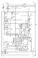
- FIG. 1schematically illustrates an embodiment of a portion of a power supply control system in accordance with the present invention
- FIG. 2schematically illustrates an embodiment of a portion of the power supply control system of FIG. 1 in accordance with the present invention.
- FIG. 3is a plan view of an embodiment of a portion of a semiconductor device that includes a portion of the power supply control system of FIG. 1 in accordance with the present invention.
- current carrying electrodemeans an element of a device that carries current through the device such as a source or a drain of an MOS transistor or an emitter or a collector of a bipolar transistor or a cathode or anode of a diode
- a control electrodemeans an element of the device that controls current through the device such as a gate of an MOS transistor or a base of a bipolar transistor.
- FIG. 1schematically illustrates an embodiment of a portion of a power supply control system 10 that includes a power supply controller 25 .
- Power supply controller 25assists in providing system 10 with a high efficiency during light load conditions.
- System 10receives power, such as a DC voltage or a rectified AC voltage, between a power input 11 and a power return 12 and responsively generates a regulated output voltage between an output voltage terminal 13 and return 12 .
- System 10typically includes an energy storage inductor 14 , an energy storage capacitor 16 , a feedback network 17 , a power switch or transistor 22 that is coupled to supply charging current to inductor 14 , and a power switch or transistor 23 that is coupled to provide a discharge current for inductor 14 .
- feedback network 17includes a voltage divider formed by resistors 18 and 19 that connected in series between terminal 13 and return 12 .
- a feedback node 20is formed at the connection between resistors 18 and 19 , and generates a feedback voltage that is representative of the value of the output voltage between terminal 13 and return 12 .
- Network 17 and transistors 22 and 23typically are external to controller 25 ; however, in some embodiments transistors 22 and 23 or network 17 may be internal to controller 25 .
- Power supply controller 25includes a PWM controller 32 , a zero crossing detector 43 , a zero crossing latch 44 , a pulse generator 45 , a transient comparator 30 , an oscillator circuit or oscillator 50 , an error amplifier 28 , a reference generator or reference 26 , and an internal voltage regulator 27 .
- Controller 25receives power between a voltage input 80 and a voltage return 81 .
- Input 80generally is connected to input 11 and return 81 generally is connected to return 12 .
- Regulator 27receives the voltage from input 80 and forms an internal voltage for operating the elements within controller 25 as illustrated by the connection from an output 31 of regulator 27 to oscillator 50 .
- Reference 26is formed to generate reference voltages for operating various elements of controller 25 including a first reference voltage that is coupled to error amplifier 28 , a second reference voltage that is coupled to a hysteresis comparator 56 of oscillator 50 , and a third reference voltage that is coupled to transient comparator 30 .
- PWM controller 32is formed to generate a first PWM drive signal on an output 37 of controller 32 and a second PWM drive signal on a second output 38 of controller 32 .
- Controller 32typically includes a PWM comparator 33 , a PWM latch 34 , and PWM control logic 36 that is used in controlling the timing of the PWM drive signals on outputs 37 and 38 .
- Transistor driver 40 and inverting transistor driver 39are formed to provide a drive capability that can provide sufficient current to drive respective transistors 22 and 23 .
- Drivers 39 and 40receive the respective first and second PWM drive signals from respective outputs 37 and 38 and responsively drive respective transistors 22 and 23 with the PWM drive signals through connections to respective outputs 82 and 83 of controller 25 .
- PWM controllers and transistor driversare well known to those skilled in the art.
- Oscillator 50is formed to provide a variable frequency clock signal (CLK) on an output 62 that is used as a timing reference for PWM controller 32 .
- Oscillator 50is also formed to provide a variable frequency ramp signal (Ramp) that is used as a reference voltage by PWM controller 32 .
- Oscillator 50includes a variable frequency oscillator (VFO) 51 that is formed to generate both the variable frequency ramp (Ramp) signal and a variable frequency oscillator signal that is used to form the variable frequency clock (CLK) signal.
- Oscillator 50also includes a buffer 59 that isolates VFO 51 from controller 32 and also buffers the Ramp signal to provide sufficient drive for controller 32 .
- a pulse shaper 61 of oscillator 50receives the variable frequency oscillator signal generated by VFO 51 , sharpens the edges of the variable frequency oscillator signal, and adjusts the duty cycle to form the CLK signal.
- shaper 61adjusts the duty cycle to approximately 50-50.
- shaper 61does not alter the frequency so that the CLK signal has the same variable frequency as the variable frequency oscillator signal.
- either or both of shaper 61 and buffer 59may be omitted.
- VFO 51includes hysteresis comparator 56 , a variable current source 52 , a timing capacitor 53 , a discharge current source 58 , and a discharge switch or transistor 57 .
- the value of the current generated by variable current source 52is controlled by the value of a frequency control signal that is applied to a current control input of source 52 .
- Oscillator 50also includes a frequency control circuit 65 that is formed to generate the frequency control signal on a frequency control output 74 .
- increasing the value of the frequency control signalincreases the frequency of the Ramp signal and the frequency of the variable frequency oscillator signal of VFO 51 , thus, the frequency of the CLK signal and the corresponding operating frequency of PWM controller 32 .
- system 10For normal load conditions, system 10 operates in a continuous conduction mode (CCM). For light load conditions, the current required by the load connected between terminal 13 and return 12 (not shown) decreases. Controller 25 responsively reduces the width of the drive pulse for transistor 22 . In some cases, the load current decreases sufficiently so that a discharge current 78 through inductor 14 reaches a value that is substantially zero. This type of operation is often referred to as a discontinuous conduction mode (DCM).
- the discontinuous conduction mode (DCM)typically is identified as a cycle of the CLK signal in which discharge current 78 through inductor 14 reaches a value that is substantially zero. The DCM operation of a particular CLK cycle begins approximately after current 78 through inductor 14 reaches the substantially zero value.
- DCM operationcan occur for one cycle or for multiple cycles of the CLK signal based on current 78 becoming substantially zero for that particular cycle. As will be seen further hereinafter, the zero crossing of current 78 is detected by detector 43 . Discharge current 78 is the current through inductor 14 . The current through transistor 23 may be different than just current 78 . Thus, controller 25 is formed to be compatible with either CCM or DCM operation and continues to enable transistors 22 and 23 in the same manner during both CCM and DCM operation.
- controller 25during the first portion of the CLK cycle is the same in for either CCM or DCM operation.
- This first portion of the CLK cycleis the time that the PWM drive signal on output 37 of controller 32 is asserted.
- oscillator 50generates the variable frequency clock signal (CLK) which sets latch 34 and facilitates controller 32 asserting the PWM drive signal on output 82 to enable transistor 22 .
- Enabling transistor 22supplies a charging current 77 to inductor 14 , capacitor 16 , and any load (not shown) connected between terminal 13 and return 12 .
- Charging current 77is the current through inductor 14 .
- Asserting the CLK signalalso resets latch 44 and prevents circuit 65 from decreasing the value of the frequency control signal on output 74 of circuit 65 while the PWM drive signal on output 37 of controller 32 is asserted.
- an edge detector circuit or edge detector 76detects that the CLK signal is asserted and generates a pulse that resets latch 44 .
- Asserting the PWM drive signal on output 37also enables transistor 67 to conduct current from current source 66 to capacitor 68 thereby charging capacitor 68 and increasing the value of the frequency control signal applied to current source 52 . Increasing the frequency control signal increases the amount of current supplied by source 52 .
- Increasing the current supplied by source 52increases the current supplied to charge capacitor 53 thereby charging capacitor 53 faster and increasing the operating frequency of oscillator 50 .
- an output of comparator 56goes high thereby enabling transistor 57 to begin discharging capacitor 53 through current source 58 .
- the value of the discharge current supplied by source 58is greater than the value of the current supplied by source 52 .
- Comparator 56typically has a hysteresis input in order to prevent false triggering of comparator 56 .
- VFO 51functions as a relaxation oscillator.
- the example embodiment of VFO 51 and frequency control circuit 65 that are illustrated in FIG. 1are example implementations of VFO 51 and circuit 65 but other implementations may be possible.
- Error amplifier 28receives the feedback signal through a connection between a feedback input 84 of controller 25 and node 20 .
- amplifier 28may include a frequency compensation network 29 .
- Amplifier 28generates an error signal that is received by comparator 33 .
- Comparator 33also receives the Ramp signal from oscillator 50 .
- comparator 33resets latch 34 .
- the reset of latch 34is received by logic 36 which responsively negates the PWM drive signal on output 82 and disable transistor 22 . Negating the PWM drive signal on output 37 of controller 32 also disables transistor 67 and decouples current source 66 from capacitor 68 thereby terminating the charging of capacitor 68 .
- Logic 36also responsively generates a PWM drive signal on output 83 to enable transistor 23 to steer current 78 through transistor 23 .
- transistor 23has a body diode that may conduct some current when transistor 23 is not enabled, thus, enabling transistor 23 steers the current through transistor 23 to be controlled by transistor 23 .
- the second portion of the CLK cycleproceeds with CCM operation.
- controller 32keeps transistor 23 enabled for the second portion of the CLK cycle and the corresponding cycle of controller 32 until oscillator 50 generates another cycle of the CLK signal and another corresponding PWM drive signal cycle. Unless current 78 reaches substantially zero, the operation continues in CCM operation as described previously.
- the value of the frequency control signalis increased by each PWM drive signal on output 37 until oscillator 50 reaches the maximum frequency of oscillator 50 .
- the maximum frequencyis selected to be the desired operating frequency in the continuous conduction mode. After the maximum frequency is reached during CCM operation, the operating frequency of oscillator 50 remains substantially constant. Thus, during CCM operation the frequency gradually increases until reaching the maximum frequency.
- a CLK cycle for DCM operationbegins similarly to CCM operation with the same operation during the first portion of the CLK cycle.
- Oscillator 50asserts the CLK signal to initiate a CLK cycle and a corresponding PWM drive signal cycle.
- Controller 32responsively asserts the PWM drive signal on output 37 which resets latch 44 and enables transistor 22 to form current 77 .
- comparator 33resets latch 34 to terminate the PWM drive signal on output 37 of controller 32 and generate a PWM drive signal on output 38 to enable transistor 23 .
- Negating the PWM drive signal on output 37 of controller 32also disables transistor 67 and decouples current source 66 from capacitor 68 thereby terminating the charging of capacitor 68 .
- Zero crossing detector 43is connected to node 21 to detect discharge current 78 through inductor 14 reaching a value that is substantially zero. When the value of current 78 becomes substantially equal to zero, the output of zero crossing detector 43 is asserted. As is well known to those skilled in the art, there may be minor offsets and variances that cause the output of detector 43 to be asserted slightly before or slightly after current 78 reaches a value of zero, however, the variance is usually small. Typically variances or errors of up to ten percent (10%) of the total cycle or period of the current through inductor 14 (the cycle of current 77 plus current 78 ) are regarded by those skilled in the art as substantially zero.
- Control logic 36receives the asserted output of detector 43 and responsively disables transistor 23 .
- the asserted output of detector 43also sets latch 44 forcing the Q output high.
- Pulse generator 45generates a pulse in response to the Q output going high.
- the high output of generator 45enables transistor 72 thereby coupling source 71 to begin discharging capacitor 68 and decreasing the value of the frequency control signal applied to current source 52 .
- Oscillator 50receives the frequency control signal and responsively decreases the operating frequency.
- Reducing the value of the voltage on capacitor 68reduces the value of the frequency control signal applied to source 52 and the current supplied by source 52 . Decreasing the current supplied to charge capacitor 53 charges capacitor 53 slower and decreases the operating frequency of the CLK and Ramp signals and increases the corresponding operating period of controller 25 . Decreasing the operating frequency of controller 25 increases the time between leading edges of the PWM drive signal on output 82 . It should be noted that the width of the PWM drive signal on output 82 is different from the period between leading edges. After disabling transistor 72 , the value of the frequency control signal remains substantially constant because of the high input impedance of source 52 . The value of the frequency control signal remains substantially constant until oscillator 50 generates another asserted CLK signal to assert another PWM drive signal.
- the amount of the change in the value of the variable frequency control signal and the corresponding frequency of the CLK signalcan be adjusted by changing the ratio of the current from sources 66 and 71 , or changing the value of either of capacitor 68 , or changing the width of the pulse formed by generator 45 .
- Outputs 37 and 38remains negated and transistors 22 and 23 remain disabled until oscillator 50 generates another cycle of the CLK signal.
- the DCM operationcontinues for each cycle of the CLK signal.
- Qup and Qdncan become equal and controller 25 operates in an equilibrium condition that keeps the operating frequency of controller 25 substantially constant.
- the duration of the pulse formed by generator 45affects where the equilibrium condition occurs. Consequently the width of the pulse generally is selected to ensure that the equilibrium can occur in a steady state condition. In one embodiment, the width of the pulse is between approximately twenty and two hundred (20-200) nanoseconds in order to remove the fixed charge from capacitor 68 to achieve the equilibrium.
- variable frequency control signalis reduced only during DCM operation.
- Transient comparator 30is used to form a quick change in the value of charging current 77 during transient conditions and during start-up conditions in order to provide the desired current to the load.
- Comparator 30compares the error signal from amplifier 28 to the third reference voltage from reference 26 .
- the value of the third reference voltageis selected to be near a value the feedback signal that represents a large change in the output voltage.
- the value of the third reference voltageis larger than the first reference voltage in order to accomplish the quick change.
- the output of comparator 30is asserted which enables transistor 70 to connect capacitor 68 to the internal operating voltage from regulator 27 . Enabling transistor 70 quickly charges capacitor 68 thereby increasing the value of the frequency control signal and the corresponding frequency of the CLK signal.
- the width of the pulses created by generator 45typically is dependent on the input voltage on input 80 . This is illustrated by the input of generator 45 that is connected to input 80 . As the voltage on input 80 increases, the width of the pulse from generator 45 may decrease. Such a decrease reduces the amount of charge removed from capacitor 68 thereby reducing the frequency dependency on the input voltage. In some embodiments, this voltage dependency is a result of current sources that are connected to receive power from input 80 .
- system 10is coupled in a buck configuration.
- controller 25may also be coupled in a any other type of dc-dc converter having a switching oscillator including boost or buck-boost configurations that have power supply controllers coupled as current mode, feed-forward, voltage mode or other types of controllers.
- oscillator 50may be used in other oscillator applications.
- regulator 27has a first terminal connected to input 80 , a second terminal connected to return 81 , and output 31 connected to a first terminal of source 52 .
- a second terminal of source 52is commonly connected to a first terminal of capacitor 53 , a drain of transistor 57 , an input of buffer 59 , and a non-inverting input of comparator 56 .
- a control input of source 52is connected to a first terminal of capacitor 68 , a drain of transistor 72 , and a source of transistors 67 and 70 .
- a second terminal of capacitor 53is connected to return 81 and to a first terminal of source 58 .
- a second terminal of source 58is connected to a source of transistor 57 .
- a gate of transistor 57is connected to the output of comparator 56 and an input of shaper 61 .
- An inverting input of comparator 56is connected to a second reference output of reference 26 .
- a second terminal of capacitor 68is connected to return 81 and to a first terminal of source 71 .
- a drain of transistor 67is connected to a first terminal of source 66 .
- a second terminal of source 66is commonly connected to a drain of transistor 70 and output 31 of regulator 27 .
- a gate of transistor 70is connected to an output of comparator 30 .
- a second terminal of source 71is connected to the source of transistor 72 .
- a gate of transistor 72is connected to the output of generator 54 which has an input connected to the Q output of latch 44 .
- a set input of latch 44is commonly connected to a control input of logic 36 and an output of detector 43 .
- a reset input of latch 44is connected to an output of detect 76 .
- An input of detector 43is connected to input 85 .
- the Ramp output of buffer 59is connected to a non-inverting input of comparator 33 .
- Output 62 of shaper 61is connected to a set input of latch 34 and to an input of detect 76 .
- a reset input of latch 34is connected to an output of comparator 33 .
- An inverting input of comparator 33is commonly connected to a non-inverting input of comparator 30 and to an output of amplifier 28 .
- An inverting input of comparator 30is connected to a third output of reference 26 .
- a first output of reference 26is connected to a non-inverting input of amplifier 28 which has an inverting input connected to input 84 .
- a Q output of latch 34is connected to an input of logic 36 and a Q bar output of latch 34 is connected to another input of logic 36 .
- Output 37 of logic 36is connected to an input of driver 39 which has an output connected to output 82 .
- Output 38 of logic 36is connected to an input of driver 40 which has an output connected to output 83 .
- FIG. 2schematically illustrates a portion of an example of an embodiment of pulse generator 45 .
- Generator 45includes an inverter 91 , a timing switch or transistor 92 , a timing capacitor 94 , a timing current source 93 , and a NOR gate 95 .
- current source 93is a controllable current source that has a current that value that is controlled by a control input 80 .
- source 93may be a voltage controlled current source that is controlled by the value of the voltage on input 80 .
- input 81is connected to input 80 to be controlled by the value of the input voltage.
- FIG. 3schematically illustrates an enlarged plan view of a portion of an embodiment of a semiconductor device 96 that is formed on a semiconductor die 97 .
- Controller 25is formed on die 97 .
- Die 97may also include other circuits that are not shown in FIG. 3 for simplicity of the drawing.
- Controller 25 and device 96are formed on die 97 by semiconductor manufacturing techniques that are well known to those skilled in the art.
- the oscillator of a power supply controllerto have a frequency that is responsive to the charging current of a inductor of a power supply system in which the power supply controller is configured. Changing the frequency of the oscillator responsively to the current through the inductor improves the efficiency of the power supply controller in light load current conditions by reducing the operating frequency of the power supply controller during DCM operation. Additionally, changing the frequency to improve efficiency does not require a lot of control logic thereby reducing the cost of the power supply controller. Additionally, the oscillation frequency is more easily controlled.
- VFO 51 , generator 45 , and circuit 65may have many different embodiments as long as the oscillator has a variable frequency that is changed in the DCM operation mode.
- circuit 65may be replaced with any type of low pass filter or integrator.
- the word “connected”is used throughout for clarity of the description, however, it is intended to have the same meaning as the word “coupled”. Accordingly, “connected” should be interpreted as including either a direct connection or an indirect connection.
Landscapes
- Engineering & Computer Science (AREA)
- Power Engineering (AREA)
- Dc-Dc Converters (AREA)
Abstract
Description
F51=(K*V74)+Fmin
- F51—is the oscillation frequency of
VFO 51, - K—is the scaling actor of VFO51,
- V74—is the value of the variable frequency control signal on
output 74, and - Fmin—is the minimum frequency of
VFO 51.
Typically, Fmin is selected to be a frequency that is greater than the audible frequency range. For the example embodiment of VFO51 illustrated inFIG. 1 , the minimum frequency can be set by configuringsource 52 to have a minimum current that results in the desired frequency.Circuit 65 includes a frequency increasecurrent source 66, a frequency increase switch ortransistor 67, a frequency decreasecurrent source 71, afrequency decrease switch 72, afrequency capacitor 68, a transient switch ortransistor 70, and afrequency control node 69 that is connected tooutput 74.
- F51—is the oscillation frequency of
Fmax=(V31*K)+Fmin
- V31—is the value of the voltage on
output 31 ofregulator 27, and - K—is the scaling actor of
VFO 51.
- V31—is the value of the voltage on
Qup=Ton*I66
- Qup—the charge stored on
capacitor 68, - Ton—the time that
output 37 is asserted, and - I66—the current of
source 66.
During DCM operation, time Ton is proportional to the square root of charging current77, thus, the charge added tocapacitor 68 and the increase in the frequency ofoscillator 50 is representative of the current throughinductor 14. As a result, the frequency ofoscillator 50 will change gradually with current77. After the PWM drive signal onoutput 37 is negated, the value of the voltage stored oncapacitor 68 and the corresponding frequency control signal remain substantially constant becausesource 52 has a high input impedance. Consequently, the operating frequency ofVFO 51 remains substantially constant aftertransistor 67 is disabled. As is well known to those skilled in the art, there may be some change in the frequency due to leakage current, however, the change is usually small and the value remains substantially constant. Typically changes of up to ten percent (10%) are regarded by those skilled in the art as substantially constant.
- Qup—the charge stored on
Qdn=T45*I71
- Qdn—the charge removed from
capacitor 68, - T45—the width of the pulse of
generator 45, and - I71—the current of
source 71.
- Qdn—the charge removed from
Claims (19)
Priority Applications (5)
| Application Number | Priority Date | Filing Date | Title |
|---|---|---|---|
| US11/001,366US7298124B2 (en) | 2004-12-01 | 2004-12-01 | PWM regulator with discontinuous mode and method therefor |
| TW094141304ATWI378334B (en) | 2004-12-01 | 2005-11-24 | Method of forming a power supply control and device therefor |
| CNB2005101272907ACN100492861C (en) | 2004-12-01 | 2005-12-01 | Method of forming a power supply control and device therefor |
| HK06111684.2AHK1091041B (en) | 2004-12-01 | 2006-10-24 | Method of forming a power supply control and device therefor |
| US13/136,604US9468560B1 (en) | 2002-01-07 | 2011-08-08 | Daneshvar support units micro and methods |
Applications Claiming Priority (1)
| Application Number | Priority Date | Filing Date | Title |
|---|---|---|---|
| US11/001,366US7298124B2 (en) | 2004-12-01 | 2004-12-01 | PWM regulator with discontinuous mode and method therefor |
Publications (2)
| Publication Number | Publication Date |
|---|---|
| US20060113974A1 US20060113974A1 (en) | 2006-06-01 |
| US7298124B2true US7298124B2 (en) | 2007-11-20 |
Family
ID=36566767
Family Applications (1)
| Application Number | Title | Priority Date | Filing Date |
|---|---|---|---|
| US11/001,366Expired - LifetimeUS7298124B2 (en) | 2002-01-07 | 2004-12-01 | PWM regulator with discontinuous mode and method therefor |
Country Status (3)
| Country | Link |
|---|---|
| US (1) | US7298124B2 (en) |
| CN (1) | CN100492861C (en) |
| TW (1) | TWI378334B (en) |
Cited By (71)
| Publication number | Priority date | Publication date | Assignee | Title |
|---|---|---|---|---|
| US20070096706A1 (en)* | 2005-10-31 | 2007-05-03 | Kabushiki Kaisha Toshiba | Power supply control method and power supply apparatus |
| US20080068030A1 (en)* | 2006-01-20 | 2008-03-20 | Snyder Warren S | Successive approximate capacitance measurement circuit |
| US20080088289A1 (en)* | 2006-10-16 | 2008-04-17 | Semtech Corporation | Switched Mode Power Supply Having Variable Minimum Switching Frequency |
| US20090009194A1 (en)* | 2007-07-03 | 2009-01-08 | Cypress Semiconductor Corporation | Normalizing capacitive sensor array signals |
| US20090108826A1 (en)* | 2007-10-25 | 2009-04-30 | Intersil Americas Inc. | Modulator with linear period stretching capability |
| US20090153127A1 (en)* | 2007-12-12 | 2009-06-18 | Monolithic Power Systems, Inc. | Method and apparatus for external control mode step down switching regulator |
| US20090153114A1 (en)* | 2007-12-12 | 2009-06-18 | Upi Semiconductor Corporation | DC-DC converters with transient response control |
| US20090219000A1 (en)* | 2008-03-03 | 2009-09-03 | Ta-Yung Yang | Switching controller with burst mode management circuit to reduce power loss and acoustic noise of power converter |
| US7721609B2 (en) | 2006-03-31 | 2010-05-25 | Cypress Semiconductor Corporation | Method and apparatus for sensing the force with which a button is pressed |
| US7737724B2 (en) | 2007-04-17 | 2010-06-15 | Cypress Semiconductor Corporation | Universal digital block interconnection and channel routing |
| US7761845B1 (en) | 2002-09-09 | 2010-07-20 | Cypress Semiconductor Corporation | Method for parameterizing a user module |
| US7765095B1 (en) | 2000-10-26 | 2010-07-27 | Cypress Semiconductor Corporation | Conditional branching in an in-circuit emulation system |
| US7770113B1 (en) | 2001-11-19 | 2010-08-03 | Cypress Semiconductor Corporation | System and method for dynamically generating a configuration datasheet |
| US20100194445A1 (en)* | 2009-01-30 | 2010-08-05 | Power Integrations, Inc. | Power supply controller with input voltage compensation for efficiency and maximum power output |
| US7774190B1 (en) | 2001-11-19 | 2010-08-10 | Cypress Semiconductor Corporation | Sleep and stall in an in-circuit emulation system |
| US20100202170A1 (en)* | 2009-02-06 | 2010-08-12 | Jin-Tae Kim | Soft-Burst Circuit For Switched-Mode Power Supplies |
| US7825688B1 (en) | 2000-10-26 | 2010-11-02 | Cypress Semiconductor Corporation | Programmable microcontroller architecture(mixed analog/digital) |
| US7834598B1 (en)* | 2007-12-21 | 2010-11-16 | Maxim Integrated Products, Inc. | Thermally optimized architecture for switching regulators |
| US7844437B1 (en) | 2001-11-19 | 2010-11-30 | Cypress Semiconductor Corporation | System and method for performing next placements and pruning of disallowed placements for programming an integrated circuit |
| US7893724B2 (en) | 2004-03-25 | 2011-02-22 | Cypress Semiconductor Corporation | Method and circuit for rapid alignment of signals |
| US20110148381A1 (en)* | 2009-12-20 | 2011-06-23 | Microsemi Corporation | Converter with crossover frequency responsive to switching frequency |
| US8026739B2 (en) | 2007-04-17 | 2011-09-27 | Cypress Semiconductor Corporation | System level interconnect with programmable switching |
| US8040321B2 (en) | 2006-07-10 | 2011-10-18 | Cypress Semiconductor Corporation | Touch-sensor with shared capacitive sensors |
| US8040266B2 (en) | 2007-04-17 | 2011-10-18 | Cypress Semiconductor Corporation | Programmable sigma-delta analog-to-digital converter |
| US8049569B1 (en) | 2007-09-05 | 2011-11-01 | Cypress Semiconductor Corporation | Circuit and method for improving the accuracy of a crystal-less oscillator having dual-frequency modes |
| US8058937B2 (en) | 2007-01-30 | 2011-11-15 | Cypress Semiconductor Corporation | Setting a discharge rate and a charge rate of a relaxation oscillator circuit |
| US8069405B1 (en) | 2001-11-19 | 2011-11-29 | Cypress Semiconductor Corporation | User interface for efficiently browsing an electronic document using data-driven tabs |
| US8067948B2 (en) | 2006-03-27 | 2011-11-29 | Cypress Semiconductor Corporation | Input/output multiplexer bus |
| US8069436B2 (en) | 2004-08-13 | 2011-11-29 | Cypress Semiconductor Corporation | Providing hardware independence to automate code generation of processing device firmware |
| US8069428B1 (en) | 2001-10-24 | 2011-11-29 | Cypress Semiconductor Corporation | Techniques for generating microcontroller configuration information |
| US8078894B1 (en) | 2007-04-25 | 2011-12-13 | Cypress Semiconductor Corporation | Power management architecture, method and configuration system |
| US8078970B1 (en) | 2001-11-09 | 2011-12-13 | Cypress Semiconductor Corporation | Graphical user interface with user-selectable list-box |
| US8085100B2 (en) | 2005-02-04 | 2011-12-27 | Cypress Semiconductor Corporation | Poly-phase frequency synthesis oscillator |
| US8085067B1 (en) | 2005-12-21 | 2011-12-27 | Cypress Semiconductor Corporation | Differential-to-single ended signal converter circuit and method |
| US8089288B1 (en) | 2006-11-16 | 2012-01-03 | Cypress Semiconductor Corporation | Charge accumulation capacitance sensor with linear transfer characteristic |
| US8089461B2 (en) | 2005-06-23 | 2012-01-03 | Cypress Semiconductor Corporation | Touch wake for electronic devices |
| US8089472B2 (en) | 2006-05-26 | 2012-01-03 | Cypress Semiconductor Corporation | Bidirectional slider with delete function |
| US8089289B1 (en) | 2007-07-03 | 2012-01-03 | Cypress Semiconductor Corporation | Capacitive field sensor with sigma-delta modulator |
| US8092083B2 (en) | 2007-04-17 | 2012-01-10 | Cypress Semiconductor Corporation | Temperature sensor with digital bandgap |
| US8103497B1 (en) | 2002-03-28 | 2012-01-24 | Cypress Semiconductor Corporation | External interface for event architecture |
| US8103496B1 (en) | 2000-10-26 | 2012-01-24 | Cypress Semicondutor Corporation | Breakpoint control in an in-circuit emulation system |
| US8120408B1 (en) | 2005-05-05 | 2012-02-21 | Cypress Semiconductor Corporation | Voltage controlled oscillator delay cell and method |
| US8130025B2 (en) | 2007-04-17 | 2012-03-06 | Cypress Semiconductor Corporation | Numerical band gap |
| US8144126B2 (en) | 2007-05-07 | 2012-03-27 | Cypress Semiconductor Corporation | Reducing sleep current in a capacitance sensing system |
| US8149048B1 (en) | 2000-10-26 | 2012-04-03 | Cypress Semiconductor Corporation | Apparatus and method for programmable power management in a programmable analog circuit block |
| US8160864B1 (en) | 2000-10-26 | 2012-04-17 | Cypress Semiconductor Corporation | In-circuit emulator and pod synchronized boot |
| US8176296B2 (en) | 2000-10-26 | 2012-05-08 | Cypress Semiconductor Corporation | Programmable microcontroller architecture |
| US8193798B1 (en)* | 2009-10-29 | 2012-06-05 | Texas Instruments Incorporated | Buck regulators with adjustable clock frequency to achieve dropout voltage reduction |
| US8286125B2 (en) | 2004-08-13 | 2012-10-09 | Cypress Semiconductor Corporation | Model for a hardware device-independent method of defining embedded firmware for programmable systems |
| US8321174B1 (en) | 2008-09-26 | 2012-11-27 | Cypress Semiconductor Corporation | System and method to measure capacitance of capacitive sensor array |
| US8358142B2 (en) | 2008-02-27 | 2013-01-22 | Cypress Semiconductor Corporation | Methods and circuits for measuring mutual and self capacitance |
| US8402313B1 (en) | 2002-05-01 | 2013-03-19 | Cypress Semiconductor Corporation | Reconfigurable testing system and method |
| TWI393335B (en)* | 2009-04-17 | 2013-04-11 | Leadtrend Tech Corp | Control method for voltage converter and related voltage converter |
| US8487639B1 (en) | 2008-11-21 | 2013-07-16 | Cypress Semiconductor Corporation | Receive demodulator for capacitive sensing |
| US8493351B2 (en) | 2006-03-30 | 2013-07-23 | Cypress Semiconductor Corporation | Apparatus and method for reducing average scan rate to detect a conductive object on a sensing device |
| US8525798B2 (en) | 2008-01-28 | 2013-09-03 | Cypress Semiconductor Corporation | Touch sensing |
| US8533677B1 (en) | 2001-11-19 | 2013-09-10 | Cypress Semiconductor Corporation | Graphical user interface for dynamically reconfiguring a programmable device |
| US8537121B2 (en) | 2006-05-26 | 2013-09-17 | Cypress Semiconductor Corporation | Multi-function slider in touchpad |
| US8536902B1 (en) | 2007-07-03 | 2013-09-17 | Cypress Semiconductor Corporation | Capacitance to frequency converter |
| US8570053B1 (en) | 2007-07-03 | 2013-10-29 | Cypress Semiconductor Corporation | Capacitive field sensor with sigma-delta modulator |
| US8570052B1 (en) | 2008-02-27 | 2013-10-29 | Cypress Semiconductor Corporation | Methods and circuits for measuring mutual and self capacitance |
| TWI419447B (en)* | 2011-01-27 | 2013-12-11 | Holtek Semiconductor Inc | Power converter and gate driver for its power transistor |
| US8866500B2 (en) | 2009-03-26 | 2014-10-21 | Cypress Semiconductor Corporation | Multi-functional capacitance sensing circuit with a current conveyor |
| US20140320094A1 (en)* | 2013-04-26 | 2014-10-30 | Richtek Technology Corporation | Control circuit for power converter and related control method |
| US9154160B2 (en) | 2006-11-14 | 2015-10-06 | Cypress Semiconductor Corporation | Capacitance to code converter with sigma-delta modulator |
| US9268441B2 (en) | 2011-04-05 | 2016-02-23 | Parade Technologies, Ltd. | Active integrator for a capacitive sense array |
| US9417728B2 (en) | 2009-07-28 | 2016-08-16 | Parade Technologies, Ltd. | Predictive touch surface scanning |
| US9448964B2 (en) | 2009-05-04 | 2016-09-20 | Cypress Semiconductor Corporation | Autonomous control in a programmable system |
| US9564902B2 (en) | 2007-04-17 | 2017-02-07 | Cypress Semiconductor Corporation | Dynamically configurable and re-configurable data path |
| US20190149137A1 (en)* | 2017-11-15 | 2019-05-16 | Semiconductor Components Industries, Llc | Oscillator, method of operating the same, and pwm controller including the same |
| US10587191B2 (en) | 2018-05-16 | 2020-03-10 | Upi Semiconductor Corp. | Dc-dc converting circuit and method for controlling the same |
Families Citing this family (31)
| Publication number | Priority date | Publication date | Assignee | Title |
|---|---|---|---|---|
| US7190143B2 (en)* | 2005-05-27 | 2007-03-13 | Rockwell Automation Technologies, Inc. | Pulse width modulation (PWM) rectifier with variable switching frequency |
| US7501715B2 (en)* | 2005-06-01 | 2009-03-10 | Delta Electronics, Inc. | Multi-output DC-DC converter |
| US7626836B2 (en)* | 2005-10-26 | 2009-12-01 | Rockwell Automation Technologies, Inc. | Method and apparatus for adjustable voltage/adjustable frequency inverter control |
| US7307485B1 (en) | 2005-11-14 | 2007-12-11 | Cypress Semiconductor Corporation | Capacitance sensor using relaxation oscillators |
| US7378826B2 (en)* | 2006-01-05 | 2008-05-27 | Linear Technology Corp. | Methods and circuits for output over-voltage reduction in switching regulators |
| US20070176903A1 (en)* | 2006-01-31 | 2007-08-02 | Dahlin Jeffrey J | Capacitive touch sensor button activation |
| JP4432920B2 (en)* | 2006-03-08 | 2010-03-17 | セイコーエプソン株式会社 | Signal transmission method, drive circuit, electro-optical device, and electronic apparatus |
| US8040142B1 (en) | 2006-03-31 | 2011-10-18 | Cypress Semiconductor Corporation | Touch detection techniques for capacitive touch sense systems |
| US7253643B1 (en) | 2006-07-19 | 2007-08-07 | Cypress Semiconductor Corporation | Uninterrupted radial capacitive sense interface |
| US9507465B2 (en) | 2006-07-25 | 2016-11-29 | Cypress Semiconductor Corporation | Technique for increasing the sensitivity of capacitive sensor arrays |
| US9766738B1 (en) | 2006-08-23 | 2017-09-19 | Cypress Semiconductor Corporation | Position and usage based prioritization for capacitance sense interface |
| US7541792B2 (en)* | 2006-10-31 | 2009-06-02 | Semiconductor Components Industries, L.L.C. | Compensated switching power supply controller and method therefor |
| US9500686B1 (en) | 2007-06-29 | 2016-11-22 | Cypress Semiconductor Corporation | Capacitance measurement system and methods |
| US8487912B1 (en) | 2008-02-01 | 2013-07-16 | Cypress Semiconductor Corporation | Capacitive sense touch device with hysteresis threshold |
| US9104273B1 (en) | 2008-02-29 | 2015-08-11 | Cypress Semiconductor Corporation | Multi-touch sensing method |
| US7969134B2 (en)* | 2008-03-27 | 2011-06-28 | Semiconductor Components Industries, Llc | Method of forming a power supply controller and structure therefor |
| US20090256534A1 (en)* | 2008-04-14 | 2009-10-15 | Twisthink, L.L.C. | Power supply control method and apparatus |
| KR101443583B1 (en)* | 2008-04-29 | 2014-11-03 | 세미컨덕터 콤포넨츠 인더스트리즈 엘엘씨 | Method for regulating an output voltage |
| US7800456B2 (en)* | 2008-05-23 | 2010-09-21 | Semiconductor Components Industries, Llc | Method of forming an oscillator circuit and structure therefor |
| US8051317B2 (en)* | 2008-06-26 | 2011-11-01 | Honeywell International, Inc. | Power supply with remotely adjustable output |
| US8300431B2 (en)* | 2010-03-05 | 2012-10-30 | Hong Kong Applied Science And Technology Research Institute Co., Ltd. | Constant-current control module using inverter filter multiplier for off-line current-mode primary-side sense isolated flyback converter |
| EP2553796A1 (en)* | 2010-04-01 | 2013-02-06 | Telefonaktiebolaget LM Ericsson (publ) | Switch control for a power converter |
| CN102364855B (en)* | 2011-06-30 | 2014-09-17 | 成都芯源系统有限公司 | Switch converter and control circuit and control method thereof |
| JP5973801B2 (en)* | 2012-06-19 | 2016-08-23 | ルネサスエレクトロニクス株式会社 | Switching regulator control circuit |
| JP5719404B2 (en)* | 2013-05-10 | 2015-05-20 | スパンション エルエルシー | Power supply voltage control circuit and power supply voltage control method |
| US9136763B2 (en) | 2013-06-18 | 2015-09-15 | Intersil Americas LLC | Audio frequency deadband system and method for switch mode regulators operating in discontinuous conduction mode |
| US20150028823A1 (en)* | 2013-07-24 | 2015-01-29 | Analog Devices Technology | Pulse width modulated power regulator with loop stabilizer |
| TWI636650B (en)* | 2017-03-17 | 2018-09-21 | 通嘉科技股份有限公司 | Controller applied to a power converter and operation method thereof |
| JP7118937B2 (en)* | 2019-09-13 | 2022-08-16 | 株式会社東芝 | switching power supply circuit |
| TWI740650B (en)* | 2020-09-17 | 2021-09-21 | 國立臺灣科技大學 | Dual mode buck converter |
| CN114362490B (en)* | 2021-12-30 | 2024-05-07 | 杭州春来科技有限公司 | Quadrupole rod power supply driving circuit |
Citations (6)
| Publication number | Priority date | Publication date | Assignee | Title |
|---|---|---|---|---|
| US5235254A (en)* | 1990-04-23 | 1993-08-10 | Pi Electronics Pte. Ltd. | Fluorescent lamp supply circuit |
| US5475579A (en)* | 1993-12-20 | 1995-12-12 | At&T Corp. | Pulse width modulator for switching power supply |
| US5481178A (en) | 1993-03-23 | 1996-01-02 | Linear Technology Corporation | Control circuit and method for maintaining high efficiency over broad current ranges in a switching regulator circuit |
| US5912552A (en)* | 1997-02-12 | 1999-06-15 | Kabushiki Kaisha Toyoda Jidoshokki Seisakusho | DC to DC converter with high efficiency for light loads |
| US6781356B1 (en) | 2003-03-24 | 2004-08-24 | System General Corp. | PWM controller having a modulator for saving power and reducing acoustic noise |
| US6853174B1 (en)* | 2003-08-11 | 2005-02-08 | Micrel, Inc. | Selective high-side and low-side current sensing in switching power supplies |
Family Cites Families (3)
| Publication number | Priority date | Publication date | Assignee | Title |
|---|---|---|---|---|
| US5959443A (en)* | 1997-11-14 | 1999-09-28 | Toko, Inc. | Controller circuit for controlling a step down switching regulator operating in discontinuous conduction mode |
| KR100351140B1 (en)* | 1999-01-08 | 2002-09-09 | 엘지전자주식회사 | Power factor correction apparatus of inverter |
| US6728117B2 (en)* | 2001-10-23 | 2004-04-27 | Koninklijke Philips Electronics N.V. | Frequency modulated self-oscillating switching power supply |
- 2004
- 2004-12-01USUS11/001,366patent/US7298124B2/ennot_activeExpired - Lifetime
- 2005
- 2005-11-24TWTW094141304Apatent/TWI378334B/enactive
- 2005-12-01CNCNB2005101272907Apatent/CN100492861C/enactiveActive
Patent Citations (6)
| Publication number | Priority date | Publication date | Assignee | Title |
|---|---|---|---|---|
| US5235254A (en)* | 1990-04-23 | 1993-08-10 | Pi Electronics Pte. Ltd. | Fluorescent lamp supply circuit |
| US5481178A (en) | 1993-03-23 | 1996-01-02 | Linear Technology Corporation | Control circuit and method for maintaining high efficiency over broad current ranges in a switching regulator circuit |
| US5475579A (en)* | 1993-12-20 | 1995-12-12 | At&T Corp. | Pulse width modulator for switching power supply |
| US5912552A (en)* | 1997-02-12 | 1999-06-15 | Kabushiki Kaisha Toyoda Jidoshokki Seisakusho | DC to DC converter with high efficiency for light loads |
| US6781356B1 (en) | 2003-03-24 | 2004-08-24 | System General Corp. | PWM controller having a modulator for saving power and reducing acoustic noise |
| US6853174B1 (en)* | 2003-08-11 | 2005-02-08 | Micrel, Inc. | Selective high-side and low-side current sensing in switching power supplies |
Non-Patent Citations (1)
| Title |
|---|
| Maxim, "Notebook CPU Step-Down Controller for Intel Mobile Voltage Positioning (IMVP-II)", 35 pages, No. 19-1960; Rev. 3; Aug. 2002; Maxim Integrated Products, Copyright 2002. |
Cited By (118)
| Publication number | Priority date | Publication date | Assignee | Title |
|---|---|---|---|---|
| US10020810B2 (en) | 2000-10-26 | 2018-07-10 | Cypress Semiconductor Corporation | PSoC architecture |
| US7765095B1 (en) | 2000-10-26 | 2010-07-27 | Cypress Semiconductor Corporation | Conditional branching in an in-circuit emulation system |
| US8103496B1 (en) | 2000-10-26 | 2012-01-24 | Cypress Semicondutor Corporation | Breakpoint control in an in-circuit emulation system |
| US9843327B1 (en) | 2000-10-26 | 2017-12-12 | Cypress Semiconductor Corporation | PSOC architecture |
| US10725954B2 (en) | 2000-10-26 | 2020-07-28 | Monterey Research, Llc | Microcontroller programmable system on a chip |
| US8736303B2 (en) | 2000-10-26 | 2014-05-27 | Cypress Semiconductor Corporation | PSOC architecture |
| US10261932B2 (en) | 2000-10-26 | 2019-04-16 | Cypress Semiconductor Corporation | Microcontroller programmable system on a chip |
| US10248604B2 (en) | 2000-10-26 | 2019-04-02 | Cypress Semiconductor Corporation | Microcontroller programmable system on a chip |
| US8160864B1 (en) | 2000-10-26 | 2012-04-17 | Cypress Semiconductor Corporation | In-circuit emulator and pod synchronized boot |
| US8358150B1 (en) | 2000-10-26 | 2013-01-22 | Cypress Semiconductor Corporation | Programmable microcontroller architecture(mixed analog/digital) |
| US8176296B2 (en) | 2000-10-26 | 2012-05-08 | Cypress Semiconductor Corporation | Programmable microcontroller architecture |
| US9766650B2 (en) | 2000-10-26 | 2017-09-19 | Cypress Semiconductor Corporation | Microcontroller programmable system on a chip with programmable interconnect |
| US8555032B2 (en) | 2000-10-26 | 2013-10-08 | Cypress Semiconductor Corporation | Microcontroller programmable system on a chip with programmable interconnect |
| US7825688B1 (en) | 2000-10-26 | 2010-11-02 | Cypress Semiconductor Corporation | Programmable microcontroller architecture(mixed analog/digital) |
| US8149048B1 (en) | 2000-10-26 | 2012-04-03 | Cypress Semiconductor Corporation | Apparatus and method for programmable power management in a programmable analog circuit block |
| US9286254B2 (en) | 2000-10-26 | 2016-03-15 | Cypress Semiconductor Corporation | Microcontroller programmable system on a chip with programmable interconnect |
| US8069428B1 (en) | 2001-10-24 | 2011-11-29 | Cypress Semiconductor Corporation | Techniques for generating microcontroller configuration information |
| US10466980B2 (en) | 2001-10-24 | 2019-11-05 | Cypress Semiconductor Corporation | Techniques for generating microcontroller configuration information |
| US8078970B1 (en) | 2001-11-09 | 2011-12-13 | Cypress Semiconductor Corporation | Graphical user interface with user-selectable list-box |
| US8370791B2 (en) | 2001-11-19 | 2013-02-05 | Cypress Semiconductor Corporation | System and method for performing next placements and pruning of disallowed placements for programming an integrated circuit |
| US7774190B1 (en) | 2001-11-19 | 2010-08-10 | Cypress Semiconductor Corporation | Sleep and stall in an in-circuit emulation system |
| US7844437B1 (en) | 2001-11-19 | 2010-11-30 | Cypress Semiconductor Corporation | System and method for performing next placements and pruning of disallowed placements for programming an integrated circuit |
| US8069405B1 (en) | 2001-11-19 | 2011-11-29 | Cypress Semiconductor Corporation | User interface for efficiently browsing an electronic document using data-driven tabs |
| US8533677B1 (en) | 2001-11-19 | 2013-09-10 | Cypress Semiconductor Corporation | Graphical user interface for dynamically reconfiguring a programmable device |
| US7770113B1 (en) | 2001-11-19 | 2010-08-03 | Cypress Semiconductor Corporation | System and method for dynamically generating a configuration datasheet |
| US8103497B1 (en) | 2002-03-28 | 2012-01-24 | Cypress Semiconductor Corporation | External interface for event architecture |
| US8402313B1 (en) | 2002-05-01 | 2013-03-19 | Cypress Semiconductor Corporation | Reconfigurable testing system and method |
| US7761845B1 (en) | 2002-09-09 | 2010-07-20 | Cypress Semiconductor Corporation | Method for parameterizing a user module |
| US7893724B2 (en) | 2004-03-25 | 2011-02-22 | Cypress Semiconductor Corporation | Method and circuit for rapid alignment of signals |
| US8286125B2 (en) | 2004-08-13 | 2012-10-09 | Cypress Semiconductor Corporation | Model for a hardware device-independent method of defining embedded firmware for programmable systems |
| US8069436B2 (en) | 2004-08-13 | 2011-11-29 | Cypress Semiconductor Corporation | Providing hardware independence to automate code generation of processing device firmware |
| US8085100B2 (en) | 2005-02-04 | 2011-12-27 | Cypress Semiconductor Corporation | Poly-phase frequency synthesis oscillator |
| US8120408B1 (en) | 2005-05-05 | 2012-02-21 | Cypress Semiconductor Corporation | Voltage controlled oscillator delay cell and method |
| US8089461B2 (en) | 2005-06-23 | 2012-01-03 | Cypress Semiconductor Corporation | Touch wake for electronic devices |
| US20070096706A1 (en)* | 2005-10-31 | 2007-05-03 | Kabushiki Kaisha Toshiba | Power supply control method and power supply apparatus |
| US8085067B1 (en) | 2005-12-21 | 2011-12-27 | Cypress Semiconductor Corporation | Differential-to-single ended signal converter circuit and method |
| US7884621B2 (en) | 2006-01-20 | 2011-02-08 | Cypress Semiconductor Corporation | Successive approximate capacitance measurement circuit |
| US20080068030A1 (en)* | 2006-01-20 | 2008-03-20 | Snyder Warren S | Successive approximate capacitance measurement circuit |
| US8067948B2 (en) | 2006-03-27 | 2011-11-29 | Cypress Semiconductor Corporation | Input/output multiplexer bus |
| US8493351B2 (en) | 2006-03-30 | 2013-07-23 | Cypress Semiconductor Corporation | Apparatus and method for reducing average scan rate to detect a conductive object on a sensing device |
| US9152284B1 (en) | 2006-03-30 | 2015-10-06 | Cypress Semiconductor Corporation | Apparatus and method for reducing average scan rate to detect a conductive object on a sensing device |
| US7721609B2 (en) | 2006-03-31 | 2010-05-25 | Cypress Semiconductor Corporation | Method and apparatus for sensing the force with which a button is pressed |
| US8537121B2 (en) | 2006-05-26 | 2013-09-17 | Cypress Semiconductor Corporation | Multi-function slider in touchpad |
| US8089472B2 (en) | 2006-05-26 | 2012-01-03 | Cypress Semiconductor Corporation | Bidirectional slider with delete function |
| US8040321B2 (en) | 2006-07-10 | 2011-10-18 | Cypress Semiconductor Corporation | Touch-sensor with shared capacitive sensors |
| US20080088289A1 (en)* | 2006-10-16 | 2008-04-17 | Semtech Corporation | Switched Mode Power Supply Having Variable Minimum Switching Frequency |
| US7471072B2 (en)* | 2006-10-16 | 2008-12-30 | Semtech Corporation | Switched mode power supply having variable minimum switching frequency |
| US9166621B2 (en) | 2006-11-14 | 2015-10-20 | Cypress Semiconductor Corporation | Capacitance to code converter with sigma-delta modulator |
| US9154160B2 (en) | 2006-11-14 | 2015-10-06 | Cypress Semiconductor Corporation | Capacitance to code converter with sigma-delta modulator |
| US8089288B1 (en) | 2006-11-16 | 2012-01-03 | Cypress Semiconductor Corporation | Charge accumulation capacitance sensor with linear transfer characteristic |
| US8058937B2 (en) | 2007-01-30 | 2011-11-15 | Cypress Semiconductor Corporation | Setting a discharge rate and a charge rate of a relaxation oscillator circuit |
| US8026739B2 (en) | 2007-04-17 | 2011-09-27 | Cypress Semiconductor Corporation | System level interconnect with programmable switching |
| US8130025B2 (en) | 2007-04-17 | 2012-03-06 | Cypress Semiconductor Corporation | Numerical band gap |
| US8092083B2 (en) | 2007-04-17 | 2012-01-10 | Cypress Semiconductor Corporation | Temperature sensor with digital bandgap |
| US8040266B2 (en) | 2007-04-17 | 2011-10-18 | Cypress Semiconductor Corporation | Programmable sigma-delta analog-to-digital converter |
| US9564902B2 (en) | 2007-04-17 | 2017-02-07 | Cypress Semiconductor Corporation | Dynamically configurable and re-configurable data path |
| US8476928B1 (en) | 2007-04-17 | 2013-07-02 | Cypress Semiconductor Corporation | System level interconnect with programmable switching |
| US7737724B2 (en) | 2007-04-17 | 2010-06-15 | Cypress Semiconductor Corporation | Universal digital block interconnection and channel routing |
| US8078894B1 (en) | 2007-04-25 | 2011-12-13 | Cypress Semiconductor Corporation | Power management architecture, method and configuration system |
| US12181943B2 (en) | 2007-05-07 | 2024-12-31 | Cypress Semiconductor Corporation | Reducing sleep current in a capacitance sensing system |
| US8976124B1 (en) | 2007-05-07 | 2015-03-10 | Cypress Semiconductor Corporation | Reducing sleep current in a capacitance sensing system |
| US10788937B2 (en) | 2007-05-07 | 2020-09-29 | Cypress Semiconductor Corporation | Reducing sleep current in a capacitance sensing system |
| US8144126B2 (en) | 2007-05-07 | 2012-03-27 | Cypress Semiconductor Corporation | Reducing sleep current in a capacitance sensing system |
| US8315832B1 (en) | 2007-07-03 | 2012-11-20 | Cypress Semiconductor Corporation | Normalizing capacitive sensor array signals |
| US20090009194A1 (en)* | 2007-07-03 | 2009-01-08 | Cypress Semiconductor Corporation | Normalizing capacitive sensor array signals |
| USRE46317E1 (en) | 2007-07-03 | 2017-02-21 | Monterey Research, Llc | Normalizing capacitive sensor array signals |
| US8086417B2 (en) | 2007-07-03 | 2011-12-27 | Cypress Semiconductor Corporation | Normalizing capacitive sensor array signals |
| US10025441B2 (en) | 2007-07-03 | 2018-07-17 | Cypress Semiconductor Corporation | Capacitive field sensor with sigma-delta modulator |
| US8089289B1 (en) | 2007-07-03 | 2012-01-03 | Cypress Semiconductor Corporation | Capacitive field sensor with sigma-delta modulator |
| US11549975B2 (en) | 2007-07-03 | 2023-01-10 | Cypress Semiconductor Corporation | Capacitive field sensor with sigma-delta modulator |
| US8570053B1 (en) | 2007-07-03 | 2013-10-29 | Cypress Semiconductor Corporation | Capacitive field sensor with sigma-delta modulator |
| US8536902B1 (en) | 2007-07-03 | 2013-09-17 | Cypress Semiconductor Corporation | Capacitance to frequency converter |
| US8049569B1 (en) | 2007-09-05 | 2011-11-01 | Cypress Semiconductor Corporation | Circuit and method for improving the accuracy of a crystal-less oscillator having dual-frequency modes |
| US7990116B2 (en)* | 2007-10-25 | 2011-08-02 | Intersil Americas Inc. | Modulator with linear period stretching capability |
| US20090108826A1 (en)* | 2007-10-25 | 2009-04-30 | Intersil Americas Inc. | Modulator with linear period stretching capability |
| US7923977B2 (en)* | 2007-12-12 | 2011-04-12 | Upi Semiconductor Corporation | DC-DC converters with transient response control |
| US7679341B2 (en)* | 2007-12-12 | 2010-03-16 | Monolithic Power Systems, Inc. | External control mode step down switching regulator |
| US20100213910A1 (en)* | 2007-12-12 | 2010-08-26 | Wei Chen | Method and apparatus for external control mode step down switching regulator |
| US8207714B2 (en) | 2007-12-12 | 2012-06-26 | Monolithic Power Systems, Inc. | Method and apparatus for external control mode step down switching regulator |
| US20090153127A1 (en)* | 2007-12-12 | 2009-06-18 | Monolithic Power Systems, Inc. | Method and apparatus for external control mode step down switching regulator |
| US20090153114A1 (en)* | 2007-12-12 | 2009-06-18 | Upi Semiconductor Corporation | DC-DC converters with transient response control |
| US7834598B1 (en)* | 2007-12-21 | 2010-11-16 | Maxim Integrated Products, Inc. | Thermally optimized architecture for switching regulators |
| US8525798B2 (en) | 2008-01-28 | 2013-09-03 | Cypress Semiconductor Corporation | Touch sensing |
| US9760192B2 (en) | 2008-01-28 | 2017-09-12 | Cypress Semiconductor Corporation | Touch sensing |
| US9423427B2 (en) | 2008-02-27 | 2016-08-23 | Parade Technologies, Ltd. | Methods and circuits for measuring mutual and self capacitance |
| US8692563B1 (en) | 2008-02-27 | 2014-04-08 | Cypress Semiconductor Corporation | Methods and circuits for measuring mutual and self capacitance |
| US8570052B1 (en) | 2008-02-27 | 2013-10-29 | Cypress Semiconductor Corporation | Methods and circuits for measuring mutual and self capacitance |
| US8358142B2 (en) | 2008-02-27 | 2013-01-22 | Cypress Semiconductor Corporation | Methods and circuits for measuring mutual and self capacitance |
| US9494628B1 (en) | 2008-02-27 | 2016-11-15 | Parade Technologies, Ltd. | Methods and circuits for measuring mutual and self capacitance |
| US20090219000A1 (en)* | 2008-03-03 | 2009-09-03 | Ta-Yung Yang | Switching controller with burst mode management circuit to reduce power loss and acoustic noise of power converter |
| US9148060B2 (en)* | 2008-03-03 | 2015-09-29 | System General Corp. | Switching controller with burst mode management circuit to reduce power loss and acoustic noise of power converter |
| US10386969B1 (en) | 2008-09-26 | 2019-08-20 | Cypress Semiconductor Corporation | System and method to measure capacitance of capacitive sensor array |
| US11029795B2 (en) | 2008-09-26 | 2021-06-08 | Cypress Semiconductor Corporation | System and method to measure capacitance of capacitive sensor array |
| US8321174B1 (en) | 2008-09-26 | 2012-11-27 | Cypress Semiconductor Corporation | System and method to measure capacitance of capacitive sensor array |
| US8487639B1 (en) | 2008-11-21 | 2013-07-16 | Cypress Semiconductor Corporation | Receive demodulator for capacitive sensing |
| US8575947B1 (en) | 2008-11-21 | 2013-11-05 | Cypress Semiconductor Corporation | Receive demodulator for capacitive sensing |
| US8222882B2 (en)* | 2009-01-30 | 2012-07-17 | Power Integrations, Inc. | Power supply controller with input voltage compensation for efficiency and maximum power output |
| US9490706B2 (en) | 2009-01-30 | 2016-11-08 | Power Integrations, Inc. | Power supply controller with input voltage compensation for efficiency and maximum power output |
| US20100194445A1 (en)* | 2009-01-30 | 2010-08-05 | Power Integrations, Inc. | Power supply controller with input voltage compensation for efficiency and maximum power output |
| US8669751B2 (en) | 2009-01-30 | 2014-03-11 | Power Integrations, Inc. | Power supply controller with input voltage compensation for efficiency and maximum power output |
| KR20100090642A (en)* | 2009-02-06 | 2010-08-16 | 페어차일드코리아반도체 주식회사 | Soft-burst circuit for switched-mode power supplies |
| US8625308B2 (en)* | 2009-02-06 | 2014-01-07 | Fairchild Korea Semiconductor Ltd. | Soft-burst circuit for switched-mode power supplies |
| US20100202170A1 (en)* | 2009-02-06 | 2010-08-12 | Jin-Tae Kim | Soft-Burst Circuit For Switched-Mode Power Supplies |
| US8866500B2 (en) | 2009-03-26 | 2014-10-21 | Cypress Semiconductor Corporation | Multi-functional capacitance sensing circuit with a current conveyor |
| US9442146B2 (en) | 2009-03-26 | 2016-09-13 | Parade Technologies, Ltd. | Multi-mode capacitive sensing device and method with current conveyor |
| TWI393335B (en)* | 2009-04-17 | 2013-04-11 | Leadtrend Tech Corp | Control method for voltage converter and related voltage converter |
| US9448964B2 (en) | 2009-05-04 | 2016-09-20 | Cypress Semiconductor Corporation | Autonomous control in a programmable system |
| US9417728B2 (en) | 2009-07-28 | 2016-08-16 | Parade Technologies, Ltd. | Predictive touch surface scanning |
| US8193798B1 (en)* | 2009-10-29 | 2012-06-05 | Texas Instruments Incorporated | Buck regulators with adjustable clock frequency to achieve dropout voltage reduction |
| US20110148381A1 (en)* | 2009-12-20 | 2011-06-23 | Microsemi Corporation | Converter with crossover frequency responsive to switching frequency |
| US8493049B2 (en)* | 2009-12-20 | 2013-07-23 | Microsemi Corporation | Converter with crossover frequency responsive to switching frequency |
| TWI419447B (en)* | 2011-01-27 | 2013-12-11 | Holtek Semiconductor Inc | Power converter and gate driver for its power transistor |
| US9268441B2 (en) | 2011-04-05 | 2016-02-23 | Parade Technologies, Ltd. | Active integrator for a capacitive sense array |
| US20140320094A1 (en)* | 2013-04-26 | 2014-10-30 | Richtek Technology Corporation | Control circuit for power converter and related control method |
| US9166477B2 (en)* | 2013-04-26 | 2015-10-20 | Richtek Technology Corporation | Control circuit for power converter and related control method |
| US10523184B2 (en)* | 2017-11-15 | 2019-12-31 | Semiconductor Components Industries, Llc | Oscillator, method of operating the same, and PWM controller including the same |
| US20190149137A1 (en)* | 2017-11-15 | 2019-05-16 | Semiconductor Components Industries, Llc | Oscillator, method of operating the same, and pwm controller including the same |
| US10587191B2 (en) | 2018-05-16 | 2020-03-10 | Upi Semiconductor Corp. | Dc-dc converting circuit and method for controlling the same |
Also Published As
| Publication number | Publication date |
|---|---|
| CN100492861C (en) | 2009-05-27 |
| US20060113974A1 (en) | 2006-06-01 |
| CN1797926A (en) | 2006-07-05 |
| TWI378334B (en) | 2012-12-01 |
| HK1091041A1 (en) | 2007-01-05 |
| TW200634472A (en) | 2006-10-01 |
Similar Documents
| Publication | Publication Date | Title |
|---|---|---|
| US7298124B2 (en) | PWM regulator with discontinuous mode and method therefor | |
| US10873263B2 (en) | Systems and methods of overvoltage protection for LED lighting | |
| US8248040B2 (en) | Time-limiting mode (TLM) for an interleaved power factor correction (PFC) converter | |
| US9912236B2 (en) | Soft start switching power supply system | |
| US9912145B2 (en) | Boost converter with short-circuit protection and method thereof | |
| US7969134B2 (en) | Method of forming a power supply controller and structure therefor | |
| US7804285B2 (en) | Control of operation of switching regulator to select PWM control or PFM control based on phase comparison | |
| USRE46333E1 (en) | High-side sensing of zero inductor current for step-down DC-DC converter | |
| US7872458B2 (en) | DC-to-DC converter | |
| KR100801498B1 (en) | Switching control circuit and self-contained DC-DC converter | |
| US9444334B2 (en) | DC/DC converter | |
| US7498793B2 (en) | Current-mode DC-to-DC-converter | |
| US20180019671A1 (en) | Noise-free control circuit for switching converter and associated control method | |
| US7109692B1 (en) | High-speed PWM control apparatus for power converters with adaptive voltage position and its driving signal generating method | |
| US20080094861A1 (en) | Predictive duty ratio generating circuit and method for synchronous boost converters operating in PFM mode | |
| US7254000B1 (en) | Over voltage protection scheme for synchronous buck converter | |
| JPH10225105A (en) | Dc-dc converter | |
| US20160149493A1 (en) | Control circuit, control method and switch-type converter | |
| US8310222B2 (en) | Method of forming a power supply controller and structure therefor | |
| US12218592B2 (en) | Control circuit for DC/DC converter | |
| US11081957B2 (en) | Power converter with multi-mode timing control | |
| TWI482403B (en) | Dc-dc converter operating in pulse width modulation mode or pulse-skipping mode and switching method thereof | |
| CN119787816B (en) | Buck converter in COT mode | |
| US12218590B2 (en) | Soft start for Buck converter | |
| HK1091041B (en) | Method of forming a power supply control and device therefor |
Legal Events
| Date | Code | Title | Description |
|---|---|---|---|
| AS | Assignment | Owner name:SEMICONDUCTOR COMPONENTS INDUSTRIES, L.L.C. OF, AR Free format text:ASSIGNMENT OF ASSIGNORS INTEREST;ASSIGNORS:KAN, KWOK KEI TOBY;LEUNG, TAK MING;REEL/FRAME:016057/0771 Effective date:20041116 | |
| AS | Assignment | Owner name:JPMORGAN CHASE BANK, N.A., NEW YORK Free format text:ASSIGNMENT OF ASSIGNORS INTEREST;ASSIGNOR:SEMICONDUCTOR COMPONENTS INDUSTRIES, LLC;REEL/FRAME:016183/0001 Effective date:20050118 | |
| STCF | Information on status: patent grant | Free format text:PATENTED CASE | |
| FPAY | Fee payment | Year of fee payment:4 | |
| FPAY | Fee payment | Year of fee payment:8 | |
| AS | Assignment | Owner name:DEUTSCHE BANK AG NEW YORK BRANCH, NEW YORK Free format text:SECURITY INTEREST;ASSIGNOR:SEMICONDUCTOR COMPONENTS INDUSTRIES, LLC;REEL/FRAME:038620/0087 Effective date:20160415 | |
| AS | Assignment | Owner name:SEMICONDUCTOR COMPONENTS INDUSTRIES, LLC, ARIZONA Free format text:RELEASE BY SECURED PARTY;ASSIGNOR:JPMORGAN CHASE BANK, N.A., AS ADMINISTRATIVE AGENT AND COLLATERAL AGENT;REEL/FRAME:038631/0345 Effective date:20100511 Owner name:SEMICONDUCTOR COMPONENTS INDUSTRIES, LLC, ARIZONA Free format text:RELEASE BY SECURED PARTY;ASSIGNOR:JPMORGAN CHASE BANK, N.A. (ON ITS BEHALF AND ON BEHALF OF ITS PREDECESSOR IN INTEREST, CHASE MANHATTAN BANK);REEL/FRAME:038632/0074 Effective date:20160415 | |
| AS | Assignment | Owner name:DEUTSCHE BANK AG NEW YORK BRANCH, AS COLLATERAL AG Free format text:CORRECTIVE ASSIGNMENT TO CORRECT THE INCORRECT PATENT NUMBER 5859768 AND TO RECITE COLLATERAL AGENT ROLE OF RECEIVING PARTY IN THE SECURITY INTEREST PREVIOUSLY RECORDED ON REEL 038620 FRAME 0087. ASSIGNOR(S) HEREBY CONFIRMS THE SECURITY INTEREST;ASSIGNOR:SEMICONDUCTOR COMPONENTS INDUSTRIES, LLC;REEL/FRAME:039853/0001 Effective date:20160415 Owner name:DEUTSCHE BANK AG NEW YORK BRANCH, AS COLLATERAL AGENT, NEW YORK Free format text:CORRECTIVE ASSIGNMENT TO CORRECT THE INCORRECT PATENT NUMBER 5859768 AND TO RECITE COLLATERAL AGENT ROLE OF RECEIVING PARTY IN THE SECURITY INTEREST PREVIOUSLY RECORDED ON REEL 038620 FRAME 0087. ASSIGNOR(S) HEREBY CONFIRMS THE SECURITY INTEREST;ASSIGNOR:SEMICONDUCTOR COMPONENTS INDUSTRIES, LLC;REEL/FRAME:039853/0001 Effective date:20160415 | |
| MAFP | Maintenance fee payment | Free format text:PAYMENT OF MAINTENANCE FEE, 12TH YEAR, LARGE ENTITY (ORIGINAL EVENT CODE: M1553); ENTITY STATUS OF PATENT OWNER: LARGE ENTITY Year of fee payment:12 | |
| AS | Assignment | Owner name:FAIRCHILD SEMICONDUCTOR CORPORATION, ARIZONA Free format text:RELEASE OF SECURITY INTEREST IN PATENTS RECORDED AT REEL 038620, FRAME 0087;ASSIGNOR:DEUTSCHE BANK AG NEW YORK BRANCH, AS COLLATERAL AGENT;REEL/FRAME:064070/0001 Effective date:20230622 Owner name:SEMICONDUCTOR COMPONENTS INDUSTRIES, LLC, ARIZONA Free format text:RELEASE OF SECURITY INTEREST IN PATENTS RECORDED AT REEL 038620, FRAME 0087;ASSIGNOR:DEUTSCHE BANK AG NEW YORK BRANCH, AS COLLATERAL AGENT;REEL/FRAME:064070/0001 Effective date:20230622 |