US7298024B2 - Transparent amorphous carbon structure in semiconductor devices - Google Patents
Transparent amorphous carbon structure in semiconductor devicesDownload PDFInfo
- Publication number
- US7298024B2 US7298024B2US11/458,642US45864206AUS7298024B2US 7298024 B2US7298024 B2US 7298024B2US 45864206 AUS45864206 AUS 45864206AUS 7298024 B2US7298024 B2US 7298024B2
- Authority
- US
- United States
- Prior art keywords
- amorphous carbon
- carbon layer
- layer
- electronic device
- memory
- Prior art date
- Legal status (The legal status is an assumption and is not a legal conclusion. Google has not performed a legal analysis and makes no representation as to the accuracy of the status listed.)
- Expired - Lifetime
Links
Images


Classifications
- H—ELECTRICITY
- H01—ELECTRIC ELEMENTS
- H01L—SEMICONDUCTOR DEVICES NOT COVERED BY CLASS H10
- H01L21/00—Processes or apparatus adapted for the manufacture or treatment of semiconductor or solid state devices or of parts thereof
- H01L21/02—Manufacture or treatment of semiconductor devices or of parts thereof
- H01L21/02104—Forming layers
- H01L21/02107—Forming insulating materials on a substrate
- H01L21/02109—Forming insulating materials on a substrate characterised by the type of layer, e.g. type of material, porous/non-porous, pre-cursors, mixtures or laminates
- H01L21/02112—Forming insulating materials on a substrate characterised by the type of layer, e.g. type of material, porous/non-porous, pre-cursors, mixtures or laminates characterised by the material of the layer
- H01L21/02115—Forming insulating materials on a substrate characterised by the type of layer, e.g. type of material, porous/non-porous, pre-cursors, mixtures or laminates characterised by the material of the layer the material being carbon, e.g. alpha-C, diamond or hydrogen doped carbon
- H—ELECTRICITY
- H01—ELECTRIC ELEMENTS
- H01L—SEMICONDUCTOR DEVICES NOT COVERED BY CLASS H10
- H01L21/00—Processes or apparatus adapted for the manufacture or treatment of semiconductor or solid state devices or of parts thereof
- H01L21/02—Manufacture or treatment of semiconductor devices or of parts thereof
- H01L21/02104—Forming layers
- H01L21/02365—Forming inorganic semiconducting materials on a substrate
- H01L21/02367—Substrates
- H01L21/0237—Materials
- H01L21/02422—Non-crystalline insulating materials, e.g. glass, polymers
- H—ELECTRICITY
- H01—ELECTRIC ELEMENTS
- H01L—SEMICONDUCTOR DEVICES NOT COVERED BY CLASS H10
- H01L21/00—Processes or apparatus adapted for the manufacture or treatment of semiconductor or solid state devices or of parts thereof
- H01L21/02—Manufacture or treatment of semiconductor devices or of parts thereof
- H01L21/027—Making masks on semiconductor bodies for further photolithographic processing not provided for in group H01L21/18 or H01L21/34
- H01L21/033—Making masks on semiconductor bodies for further photolithographic processing not provided for in group H01L21/18 or H01L21/34 comprising inorganic layers
- H01L21/0332—Making masks on semiconductor bodies for further photolithographic processing not provided for in group H01L21/18 or H01L21/34 comprising inorganic layers characterised by their composition, e.g. multilayer masks, materials
- H—ELECTRICITY
- H01—ELECTRIC ELEMENTS
- H01L—SEMICONDUCTOR DEVICES NOT COVERED BY CLASS H10
- H01L21/00—Processes or apparatus adapted for the manufacture or treatment of semiconductor or solid state devices or of parts thereof
- H01L21/02—Manufacture or treatment of semiconductor devices or of parts thereof
- H01L21/04—Manufacture or treatment of semiconductor devices or of parts thereof the devices having potential barriers, e.g. a PN junction, depletion layer or carrier concentration layer
- H01L21/18—Manufacture or treatment of semiconductor devices or of parts thereof the devices having potential barriers, e.g. a PN junction, depletion layer or carrier concentration layer the devices having semiconductor bodies comprising elements of Group IV of the Periodic Table or AIIIBV compounds with or without impurities, e.g. doping materials
- H01L21/30—Treatment of semiconductor bodies using processes or apparatus not provided for in groups H01L21/20 - H01L21/26
- H01L21/302—Treatment of semiconductor bodies using processes or apparatus not provided for in groups H01L21/20 - H01L21/26 to change their surface-physical characteristics or shape, e.g. etching, polishing, cutting
- H01L21/306—Chemical or electrical treatment, e.g. electrolytic etching
- H01L21/308—Chemical or electrical treatment, e.g. electrolytic etching using masks
- H01L21/3081—Chemical or electrical treatment, e.g. electrolytic etching using masks characterised by their composition, e.g. multilayer masks, materials
- H—ELECTRICITY
- H10—SEMICONDUCTOR DEVICES; ELECTRIC SOLID-STATE DEVICES NOT OTHERWISE PROVIDED FOR
- H10B—ELECTRONIC MEMORY DEVICES
- H10B12/00—Dynamic random access memory [DRAM] devices
- H10B12/01—Manufacture or treatment
- H10B12/02—Manufacture or treatment for one transistor one-capacitor [1T-1C] memory cells
- H10B12/03—Making the capacitor or connections thereto
- H10B12/033—Making the capacitor or connections thereto the capacitor extending over the transistor
- H—ELECTRICITY
- H01—ELECTRIC ELEMENTS
- H01L—SEMICONDUCTOR DEVICES NOT COVERED BY CLASS H10
- H01L21/00—Processes or apparatus adapted for the manufacture or treatment of semiconductor or solid state devices or of parts thereof
- H01L21/02—Manufacture or treatment of semiconductor devices or of parts thereof
- H01L21/02104—Forming layers
- H01L21/02107—Forming insulating materials on a substrate
- H01L21/02109—Forming insulating materials on a substrate characterised by the type of layer, e.g. type of material, porous/non-porous, pre-cursors, mixtures or laminates
- H01L21/02112—Forming insulating materials on a substrate characterised by the type of layer, e.g. type of material, porous/non-porous, pre-cursors, mixtures or laminates characterised by the material of the layer
- H01L21/02123—Forming insulating materials on a substrate characterised by the type of layer, e.g. type of material, porous/non-porous, pre-cursors, mixtures or laminates characterised by the material of the layer the material containing silicon
- H01L21/02126—Forming insulating materials on a substrate characterised by the type of layer, e.g. type of material, porous/non-porous, pre-cursors, mixtures or laminates characterised by the material of the layer the material containing silicon the material containing Si, O, and at least one of H, N, C, F, or other non-metal elements, e.g. SiOC, SiOC:H or SiONC
- H01L21/0214—Forming insulating materials on a substrate characterised by the type of layer, e.g. type of material, porous/non-porous, pre-cursors, mixtures or laminates characterised by the material of the layer the material containing silicon the material containing Si, O, and at least one of H, N, C, F, or other non-metal elements, e.g. SiOC, SiOC:H or SiONC the material being a silicon oxynitride, e.g. SiON or SiON:H
- H—ELECTRICITY
- H01—ELECTRIC ELEMENTS
- H01L—SEMICONDUCTOR DEVICES NOT COVERED BY CLASS H10
- H01L21/00—Processes or apparatus adapted for the manufacture or treatment of semiconductor or solid state devices or of parts thereof
- H01L21/02—Manufacture or treatment of semiconductor devices or of parts thereof
- H01L21/02104—Forming layers
- H01L21/02107—Forming insulating materials on a substrate
- H01L21/02109—Forming insulating materials on a substrate characterised by the type of layer, e.g. type of material, porous/non-porous, pre-cursors, mixtures or laminates
- H01L21/022—Forming insulating materials on a substrate characterised by the type of layer, e.g. type of material, porous/non-porous, pre-cursors, mixtures or laminates the layer being a laminate, i.e. composed of sublayers, e.g. stacks of alternating high-k metal oxides
- H—ELECTRICITY
- H01—ELECTRIC ELEMENTS
- H01L—SEMICONDUCTOR DEVICES NOT COVERED BY CLASS H10
- H01L21/00—Processes or apparatus adapted for the manufacture or treatment of semiconductor or solid state devices or of parts thereof
- H01L21/02—Manufacture or treatment of semiconductor devices or of parts thereof
- H01L21/02104—Forming layers
- H01L21/02107—Forming insulating materials on a substrate
- H01L21/02225—Forming insulating materials on a substrate characterised by the process for the formation of the insulating layer
- H01L21/0226—Forming insulating materials on a substrate characterised by the process for the formation of the insulating layer formation by a deposition process
- H01L21/02263—Forming insulating materials on a substrate characterised by the process for the formation of the insulating layer formation by a deposition process deposition from the gas or vapour phase
- H01L21/02271—Forming insulating materials on a substrate characterised by the process for the formation of the insulating layer formation by a deposition process deposition from the gas or vapour phase deposition by decomposition or reaction of gaseous or vapour phase compounds, i.e. chemical vapour deposition
- H01L21/02274—Forming insulating materials on a substrate characterised by the process for the formation of the insulating layer formation by a deposition process deposition from the gas or vapour phase deposition by decomposition or reaction of gaseous or vapour phase compounds, i.e. chemical vapour deposition in the presence of a plasma [PECVD]
- H—ELECTRICITY
- H01—ELECTRIC ELEMENTS
- H01L—SEMICONDUCTOR DEVICES NOT COVERED BY CLASS H10
- H01L21/00—Processes or apparatus adapted for the manufacture or treatment of semiconductor or solid state devices or of parts thereof
- H01L21/02—Manufacture or treatment of semiconductor devices or of parts thereof
- H01L21/02104—Forming layers
- H01L21/02365—Forming inorganic semiconducting materials on a substrate
- H01L21/02367—Substrates
- H01L21/0237—Materials
- H—ELECTRICITY
- H01—ELECTRIC ELEMENTS
- H01L—SEMICONDUCTOR DEVICES NOT COVERED BY CLASS H10
- H01L21/00—Processes or apparatus adapted for the manufacture or treatment of semiconductor or solid state devices or of parts thereof
- H01L21/02—Manufacture or treatment of semiconductor devices or of parts thereof
- H01L21/02104—Forming layers
- H01L21/02365—Forming inorganic semiconducting materials on a substrate
- H01L21/02436—Intermediate layers between substrates and deposited layers
- H01L21/02439—Materials
- H—ELECTRICITY
- H01—ELECTRIC ELEMENTS
- H01L—SEMICONDUCTOR DEVICES NOT COVERED BY CLASS H10
- H01L21/00—Processes or apparatus adapted for the manufacture or treatment of semiconductor or solid state devices or of parts thereof
- H01L21/02—Manufacture or treatment of semiconductor devices or of parts thereof
- H01L21/02104—Forming layers
- H01L21/02365—Forming inorganic semiconducting materials on a substrate
- H01L21/02436—Intermediate layers between substrates and deposited layers
- H01L21/02494—Structure
- H01L21/02496—Layer structure
- H01L21/02505—Layer structure consisting of more than two layers
- H—ELECTRICITY
- H01—ELECTRIC ELEMENTS
- H01L—SEMICONDUCTOR DEVICES NOT COVERED BY CLASS H10
- H01L21/00—Processes or apparatus adapted for the manufacture or treatment of semiconductor or solid state devices or of parts thereof
- H01L21/02—Manufacture or treatment of semiconductor devices or of parts thereof
- H01L21/02104—Forming layers
- H01L21/02365—Forming inorganic semiconducting materials on a substrate
- H01L21/02518—Deposited layers
- H01L21/02521—Materials
- H01L21/02524—Group 14 semiconducting materials
- H01L21/02527—Carbon, e.g. diamond-like carbon
- H—ELECTRICITY
- H01—ELECTRIC ELEMENTS
- H01L—SEMICONDUCTOR DEVICES NOT COVERED BY CLASS H10
- H01L21/00—Processes or apparatus adapted for the manufacture or treatment of semiconductor or solid state devices or of parts thereof
- H01L21/02—Manufacture or treatment of semiconductor devices or of parts thereof
- H01L21/02104—Forming layers
- H01L21/02365—Forming inorganic semiconducting materials on a substrate
- H01L21/02612—Formation types
- H01L21/02617—Deposition types
- H01L21/0262—Reduction or decomposition of gaseous compounds, e.g. CVD
Definitions
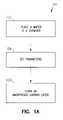
- the present inventionrelates generally to semiconductor devices, more particularly to masking structures in the semiconductor devices.
- Semiconductor devicessuch as memory devices reside in many computers and electronic products to store data.
- a typical semiconductor devicehas many layers of different materials formed on a semiconductor wafer.
- the layersgo through many processes. For example, a patterning process puts patterns on the layers. Some patterning processes use a mask to transfer patterns from the mask to the layers underneath the mask.
- Some conventional masksare made of amorphous carbon.
- an amorphous carbon mask at some thicknessmay have a high absorption of optical light, causing the amorphous carbon mask inapplicable for some processes.
- FIG. 1Ais a flow chart showing a method of forming an amorphous carbon layer according an embodiment of the invention.
- FIG. 1Bis graph showing an extinction coefficient (k) at an exemplary wavelength versus deposition temperature of a transparent amorphous carbon layer according to an embodiment of the invention.
- FIG. 1Cis graph showing an extinction coefficient (k) at exemplary temperatures versus range of wavelengths of a transparent amorphous carbon according to an embodiment of the invention.
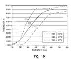
- FIG. 1Dis graph showing a transmission percentage versus a range of wavelengths of several transparent amorphous carbon layers at exemplary temperatures and exemplary thicknesses according to an embodiment of the invention.
- FIG. 1Eis graph showing an exemplary deposition rate versus a temperature range of a method of forming a transparent amorphous carbon layer according to an embodiment of the invention.
- FIG. 2 through FIG. 10show cross-sections of a device during various processing stages according to embodiments of the invention.
- FIG. 11 through FIG. 19show cross-sections of a memory device during various processing stages according to embodiments of the invention.
- FIG. 20shows a system according to an embodiment of the invention.
- FIG. 21is a simplified block diagram for an embodiment of a memory device in which an amorphous carbon layer, which is substantially transparent, is employed using an embodiment for an amorphous carbon layer according to the teachings of the present invention.
- FIG. 22illustrates a block diagram for an embodiment of an electronic system having devices in which an amorphous carbon layer, which is substantially transparent, is employed using an embodiment for an amorphous carbon layer according to the teachings of the present invention.
- FIG. 1Ais flowchart showing a method of forming an amorphous carbon layer according to an embodiment of the invention.
- Method 100forms an amorphous carbon layer having a low absorption coefficient such that the amorphous carbon layer is transparent in visible light range.
- the visible light rangeis the range (optical range) of the electromagnetic spectrum having light (electromagnetic radiation) visible to human eyes.
- the visible light rangeincludes any light having a wavelength between about 400 nm (nanometers) and about 700 nm.
- the non-visible light rangeis the range of the entire electromagnetic spectrum minus the visible light range.
- Some examples of the non-visible light rangeinclude electromagnetic radiations with wavelengths between 700 nm and one millimeter (infrared light), wavelengths between 10 nm and 400 nm (ultraviolet light), and wavelengths between 0.01 nm and 10 nm (X-ray).
- the amorphous carbon layer is transparent in visible light rangemeans that the amorphous carbon layer has a substantially low extinction coefficient (k) in which k has a range between about 0.15 and about 0.001 at wavelength of 633 nm.
- the amorphous carbon layer transparent in visible light rangeis an amorphous carbon layer formed at a temperature from about 150° C. to about 500° C. such that the amorphous carbon layer has an extinction coefficient (k) between about 0.15 and about 0.001 at wavelength of 633 nm.
- a waferis placed in a chamber.
- the chamberis a chemical vapor deposition chamber and the wafer is a semiconductor wafer.
- the chamberis a plasma enhanced chemical vapor deposition (PECVD) chamber.
- the parametersare set for the process of forming an amorphous carbon layer according to the invention.
- the parametersinclude temperature, gas mixture, gas flow rate, power, and pressure.
- the temperature in the chamberis set to a selected temperature.
- the selected temperatureis any temperature from about 150° C. to about 500° C. In some embodiments, the temperature is set between about 200° C. and below 300° C. In other embodiments, the temperature is set between about 225° C. and about 375° C.
- a process gas including propylene(C 3 H 6 ) is introduced into the chamber at a flow rate.
- the flow rate of the propyleneis set between about 500 standard cubic centimeters per minute (sccm) and about 3000 sccm.
- An additional gas including heliummay be also introduced into the chamber at a flow rate.
- the flow rate of the heliumis set between about 250 sccm and about 1000 sccm. Further, embodiments exist where at least one of the other hydrocarbon gases is used as the process gas.
- hydrocarbon gasesexamples include CH 4 , C 2 H 2 , C 2 H 4 , C 2 H 6 , and C 3 H 8 .
- Heliummay also be used in combination with at least one of these hydrocarbon gases.
- the gas mixturemay be either one gas only or a combination of at least two gases.
- the gas mixturemay be either propylene (C 3 H 6 ) only or a combination of propylene and helium.
- the gas mixturemay be at least one of the propylene, CH 4 , C 2 H 2 , C 2 H 4 , C 2 H 6 , and C 3 H 8 .
- the gas mixturemay be at least one of the propylene, CH 4 , C 2 H 2 , C 2 H 4 , C 2 H 6 , and C 3 H 8 plus helium.
- the chamberis subjected to a radio frequency (RF) power and a pressure.
- RFradio frequency
- the radio frequency poweris set between about 450 Watts and about 1000 Watts
- the pressureis set between about 3.0 Torr and about 7.0 Torr.
- an amorphous carbon layeris formed as a deposited layer over the wafer.
- the amorphous carbon layeris transparent in visible light range.
- the amorphous carbon layer formed by method 100has an extinction coefficient (k) between about 0.15 and about 0.001 at wavelength of 633 nm.
- the amorphous carbon layer formed by method 100is transparent in visible light range, the amorphous carbon layer formed by method 100 is also referred to as a transparent amorphous carbon layer.
- the transparent amorphous carbon layerrefers to an amorphous carbon layer formed according method 100 in which the temperature is set from about 150° C. to about 500° C.
- the transparency of the amorphous carbon layer formed by method 100depends in part on the temperature set during the process.
- the transparency of the amorphous carbon layer formed to a specific thickness at a lower temperatureis more transparent than the amorphous carbon layer formed to that specific thickness at a higher temperature.
- the amorphous carbon layer formed to a thickness at 150° C.is more transparent than the amorphous carbon layer formed to the same thickness at 500° C.
- the transparent amorphous carbon layer formed by method 100may be used in semiconductor devices such as memory devices and microprocessors.
- the transparent amorphous carbon layer formed by method 100may be included in a structure of semiconductor devices as an insulating layer or an antireflective layer.
- the transparent amorphous carbon layer formed by method 100may also be used as a mask in an etching process during manufacturing of semiconductor devices.
- FIG. 1Bis graph showing extinction coefficient (k) at an exemplary wavelength versus deposition temperature of a transparent amorphous carbon layer according to an embodiment of the invention.
- the graph of FIG. 1Bshows the extinction coefficient of the transparent amorphous carbon layer formed according to the method described in FIG. 1A .
- curve 150shows the transparent amorphous layer having an extinction coefficient k ranging from about 0.15 to about 0.001 at wavelength of 633 nm when the transparent amorphous layer is formed (or deposited) at a temperature from about 150° C. to about 500° C.
- curve 150has an exemplary shape. In some embodiments, curve 150 may have a shape different from the shape shown in FIG. 1B .
- FIG. 1Cis graph showing extinction coefficient (k) at exemplary temperatures versus a range of wavelengths of a transparent amorphous carbon according to an embodiment of the invention.
- the graph of FIG. 1Cshows the extinction coefficient of the transparent amorphous carbon layer formed according to the method described in FIG. 1A .
- curve 161shows extinction coefficient (k) versus a range of wavelengths of a transparent amorphous carbon formed at an exemplary temperature of 375° C.
- Curve 162shows extinction coefficient versus a range of wavelengths of another transparent amorphous carbon formed at an exemplary temperature of 225° C.
- FIG. 1Dis graph showing transmission percentage versus a range of wavelengths of several transparent amorphous carbon layers at exemplary temperatures and exemplary thicknesses according to an embodiment of the invention.
- the graph of FIG. 1Dshows exemplary transmission percentages of the transparent amorphous carbon layer formed according to the method described in FIG. 1A .
- curves 171 , 172 , and 173show transmission percentage versus a range of wavelengths for three different amorphous carbon layers formed to different thicknesses at different temperatures.
- Curve 171shows transmission percentage versus a range of wavelengths of a transparent amorphous carbon layer formed to a thickness of 3000 Angstroms at a temperature of 225° C.
- Curve 172shows transmission percentage versus the range of wavelengths of a transparent amorphous carbon layer formed to a thickness of 3000 Angstroms at a temperature of 375° C.
- Curve 173shows transmission percentage versus the range of wavelengths of a transparent amorphous carbon layer formed to a thickness of 7000 Angstroms at a temperature of 375° C.
- FIG. 1Dshows that the transmission increases when the thicknesses, or the temperature, or both decreases.
- FIG. 1Eis graph showing exemplary deposition rate versus a temperature range of a method of forming a transparent amorphous carbon layer according to an embodiment of the invention.
- the graph of FIG. 1Eshows exemplary deposition rate of the transparent amorphous carbon layer formed according to the method described in FIG. 1A .
- FIG. 1Eshows that the deposition rate is inversely proportional to the temperature. For example, at a temperature of 250° C., the deposition rate is about 2800 Angstroms per minute. As another example, at a temperature of 400° C., the deposition rate is about 2100 Angstroms per minute.
- FIG. 2 through FIG. 10show a device 200 during various processing stages according to embodiments of the invention.
- FIG. 2shows a cross-section of a device 200 including a substrate 210 .
- Substrate 210may represent a part of a wafer, or may be a wafer itself.
- the wafermay be a semiconductor wafer such as a silicon wafer.
- Substrate 210may also be a structure or a layer formed on a wafer.
- Substrate 210may include at least one of a non-conducting material, a conducting material, and a semiconducting material. Examples of non-conducting materials include oxide (e.g., SiO 2 , Al 2 O 3 ), nitride (e.g., Si 3 N 4 ), and glass (borophosphosilicate glass-BPSG).
- oxidee.g., SiO 2 , Al 2 O 3
- nitridee.g., Si 3 N 4
- glassborophosphosilicate glass-BPSG
- substrate 210includes a semiconductor material.
- Substrate 210has a surface 212 in which alignment marks 214 are formed.
- Alignment marks 214serves as reference points or coordinates of substrate (wafer) 210 .
- the alignment marks 214are used to align or position substrate 210 such that structures and layers on substrate 210 can be accurately aligned with each other or with substrate 210 .
- FIG. 3shows device 200 with a device structure 320 formed over substrate 210 .
- Device structure 320includes multiple layers 322 , 324 , and 326 . Each of these multiple layers may include at least one of a non-conducting material, semiconducting material, and a conducting material.
- layer 322may be an oxide layer
- layer 324may be a metal layer or a layer having a compound of metal and silicon
- layer 326may be a nitride layer.
- multiple layers 322 , 324 , and 326are arranged in an order different from the order shown in FIG. 3 .
- Multiple layers 322 , 324 , and 326are formed by growing or deposition or by other known processes.
- one or more of the layers 322 , 324 , and 326is omitted from device structure 320 . In other embodiments, one or more additional layers similar to layers 322 , 324 , and 326 are added to device structure 320 .
- Device structure 320has a thickness T 3 . In some embodiments, T 3 is at least 40000 Angstroms.
- FIG. 4Ashows device 200 with a mask (layer) 430 formed over device structure 320 .
- Mask 430is made of carbon.
- the carbonis amorphous carbon.
- mask 430is also referred to as amorphous carbon layer 430 .
- Amorphous carbon layer 430may be formed by a method similar to method 100 described in FIG. 1A .
- Amorphous carbon layer 430has a thickness T 4 .
- T 4can be any thickness. In an embodiment, T 4 has a thickness of about 1500 Angstroms. In another embodiment, T 4 has a thickness of about 2000 Angstroms. In some embodiments, T 4 is at least 4000 Angstroms. In various embodiments, T 4 has a thickness that ranges from about 1000 Angstroms to about 12000 Angstroms.
- Amorphous carbon layer 430has a low absorption coefficient such that amorphous carbon layer 430 is transparent in visible light range. In some embodiments, amorphous carbon layer 430 has an extinction coefficient (k) between about 0.15 and about 0.001 at wavelength of 633 nm.
- amorphous carbon layer 430Since amorphous carbon layer 430 is transparent in visible light range, amorphous carbon layer 430 does not substantially absorb or reflect the light in the visible light range. Therefore, the transparency in visible light range property of amorphous carbon layer 430 improves the reading of alignment marks 214 ( FIG. 2 ) on substrate 210 during the alignment of substrate 210 . Further, since amorphous carbon layer 430 is transparent in visible light range, the thickness of amorphous carbon layer 430 may not be limited. Thus, amorphous carbon layer 430 may be formed with a thickness to properly etch device structure 320 while allowing an accurate reading of the alignment marks such as alignment marks 214 .
- the conventional amorphous carbonmay have a thickness limitation for some processes. For example, some process may require a mask with a specific thickness, using a conventional amorphous carbon layer with the specific thickness may cause difficulty in reading the alignment marks or may result in inaccurate reading because of the high absorption property of the conventional amorphous carbon layer. Therefore, because of the low absorption property, amorphous carbon layer 430 is useful in processes that may require a mask with a specific thickness in which a conventional amorphous carbon mask is unsuitable.
- Amorphous carbon layer 430 of device 200is formed with a thickness sufficient to properly etch a device structure such as device structure 320 .
- amorphous carbon layer 430is formed with thickness T 4 equal to or greater than about 4000 Angstroms to etch device structure 320 with thickness T 3 equal to or greater than 40000 Angstroms.
- FIG. 4Bshows device 200 with a cap layer 540 formed over amorphous carbon layer 430 .
- cap layer 540includes oxide materials. In other embodiments, cap layer 540 includes non-oxide materials.
- cap layer 540includes silicon oxynitride (Si x O y N z ) or silicon-rich oxide (Si x O y ) where x, y, and z are real numbers.
- cap layer 540includes hydrogenated silicon oxynitride (Si x O y N z :H) or hydrogenated silicon-rich oxide (Si x O y :H).
- Cap layer 540can be formed by a deposition process such as a CVD and PECVD process. In some embodiments, cap layer 540 is formed together with amorphous carbon layer 430 in the same process (same processing step) such that cap layer 540 is in situ deposited over amorphous carbon layer 430 .
- FIG. 5shows device 200 with a photoresist layer 550 formed over cap layer 540 and amorphous carbon layer 430 .
- Photoresist 550is formed using known techniques.
- cap layer 540serves as an antireflective layer for reducing the reflection to photoresist layer 550 from layers underneath amorphous carbon layer 430 during patterning of photoresist layer 550 . Reducing the reflection allows more accurate patterning of photoresist layer 550 .
- cap layer 540serves as a mask for patterning amorphous carbon layer 430 .
- cap layer 540serves as both an antireflective layer and as a mask.
- amorphous carbon layer 430forms a masking structure 560 .
- cap layer 540is omitted from masking structure 560 .
- masking structure 560further includes an additional layer formed between photoresist layer 550 and cap layer 540 .
- the additional layerserves as an antireflective layer to further enhance the photo processing performance.
- FIG. 6shows device 200 after photoresist layer 550 is patterned.
- Patterning photoresist layer 550can be performed using known techniques.
- patterned photoresist layer 550has openings 652 .
- Patterned photoresist layer 550is used as a mask to pattern cap layer 540 and amorphous carbon layer 430 .
- FIG. 7shows device 200 after the masking structure 560 is patterned.
- Patterning masking structure 560can be performed by one or more etching steps.
- cap layer 540 and amorphous carbon layer 430are etched together in one etching step.
- cap layer 540 and amorphous carbon layer 430are etched separately in different etching steps.
- each of the patterned cap layer 540 and the patterned amorphous carbon layer 430has openings that are continuous and aligned with openings 652 of photoresist layer 550 .
- the combination of layers 430 , 540 , and 550 of masking structure 560may remain and is used as a mask to etch the layers of device structure 320 .
- either photoresist layer 550 or a combination of both photoresist layer 550 and cap layer 540is removed.
- the remaining (not removed) layer, or layers, of masking structure 560is used as a mask to etch one or both of device structure 320 and substrate 210 .
- FIG. 8shows device 200 after both photoresist layer 550 and cap layer 540 are removed.
- the remaining amorphous carbon layer 430is used as a mask to etch either a portion of device structure 320 , or the entire device structure 320 .
- at least a portion of substrate 210is also etched using amorphous carbon layer 430 as a mask.
- FIG. 9shows device 200 after device structure 320 is etched. Trenches 901 are formed as a result of the etching process. In embodiments represented by FIG. 9 , trenches 901 are formed in at least portion of device structure 320 . In some embodiments, trenches 901 are formed in the entire device structure 320 and in at least a portion of substrate 210 .
- Layer 322is etched to a level 902 .
- Level 902is any level above surface 212 of substrate 210 .
- device structure 320is etched such that the etching process penetrates through layers 326 and 324 and partially into layer 324 and stopping at level 902 .
- device structure 320is etched such that level 902 can be anywhere in device structure 320 .
- the etching processpenetrates through all layers 322 , 324 , and 326 and stops at or below surface 212 of substrate 210 .
- the level at which the etching process etches into device structure 320depends on what will be formed after device structure 320 is etched. For example, device structure 320 is etched to one level if conductive interconnects will be formed and device structure 320 is etched to another level if a component such as a capacitor will be formed.
- FIG. 10shows device 100 after amorphous carbon layer 430 is removed.
- amorphous carbon layer 430is removed using an ash process with oxygen plasma.
- amorphous carbon layer 430is removed using an ash process with a combination of oxygen plasma and CF 4 .
- amorphous carbon layer 430which is transparent in visible light range, is included in masking structure 560 to use as a mask to etch device structure 320 .
- an amorphous carbon layersuch as amorphous carbon layer 430 is also included in device structure 320 .
- one of the layers 322 , 324 , and 326 of device structure 320may be an amorphous carbon layer such as amorphous carbon layer 430 .
- device structure 320may include an additional layer besides layer 322 , 324 , and 326 in which the additional layer is an amorphous carbon layer such as amorphous carbon layer 430 .
- the amorphous carbon layer within device structure 320may be used for insulating purposes, antireflection purposes, or for other purposes.
- the amorphous carbon layer of device structure 320still remains in device 200 after amorphous carbon layer 430 of masking structure 560 is removed from device 200 .
- amorphous carbon layer 430is removed as shown in FIG. 10 , other processes can be performed to device 200 to form components such as transistors, capacitors, memory cell, or an integrated circuit such as a memory device, a processor, an application specific integrated circuit, or other types of integrated circuits.
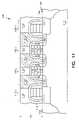
- FIG. 11 through FIG. 19show cross-sections of a memory device 1100 during various processing stages according to embodiments of the invention.
- memory device 1100includes a substrate 1102 having alignment marks 1104 formed on surface 1107 of substrate 1102 .
- a number of surface structures (gate structures) 1105( 1105 . 1 through 1105 . 4 ) are formed over substrate 1102 .
- a number of diffusion regions 1106( 1106 . 1 through 1106 . 3 ) and isolation structures 1107 . 1 and 1107 . 2 are formed.
- FIG. 11shows alignment marks 1104 without elements formed above alignment marks 1104 . However, elements such as the layers shown in FIG. 11 may be formed over alignment marks 1104 .
- Memory device 1100also includes an insulating layer 1130 and a number of contacts 1140 ( 1140 . 1 through 1140 . 3 ) extending through insulating layer 1130 .
- Each of the contacts 1140connects to one of the diffusion regions 1106 .
- a barrier layer 1145separates surface structures 1105 from insulating layer 1130 and contacts 1140 .
- Contacts 1140are made of conducting material to provide electrical connections for diffusion regions 1106 .
- Barrier layer 1145can be oxide, or nitrite, or other non-conducting materials to prevent cross-diffusion of materials between surface structures 1105 and insulating layer 1130 . In some embodiments, barrier layer 1145 is omitted.
- Insulating layer 1130provides insulation between the contacts 1140 .
- Insulating layer 1130can be a layer of silicate glass doped with one or more dopants such as boron and phosphorous or other types of doped glasses.
- insulating layer 1130can be Boronsilicate glass (BSG), or Phosphosilicate glass (PSG).
- BSGBoronsilicate glass
- PSGPhosphosilicate glass
- insulating layer 1130includes Borophosphosilicate glass (BPSG) and has a thickness T 11 . In some embodiments, T 11 is in the range of 3000 Angstroms to 5000 Angstroms.
- substrate 1102includes silicon doped with a dopant, for example boron, to make it a P-type material.
- Diffusion regions 1106are doped with a dopant, for example phosphorous, to make them an N-type material.
- substrate 1102can be an N-type material and diffusion regions 1106 can be a P-type material.
- Each of the gate structures 1105includes a number of elements: a gate dielectric (gate oxide) 1109 , a doped polysilicon layer 1112 , a silicide layer 1114 , a capping dielectric layer 1116 , and dielectric spacers 1118 .
- Silicide layer 1114can include a compound of metal and silicon such as titanium silicide, tungsten silicide, and others. All dielectrics in gate structures 1105 can include material such as silicon oxide.
- Each of the gate structures 1105is also referred to as a word line. The structure of FIG. 11 can be formed using known techniques.
- FIG. 12shows memory device 1100 after an insulating layer 1210 is formed.
- Insulating layer 1210can include BSG, PSG, or BPSG similar to insulating layer 1130 .
- Insulating layer 1210 and other structures in FIG. 12form a device structure 1220 .
- Device structure 1220has a thickness T 12 . In some embodiments, T 12 is at least 40000 Angstroms.
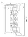
- FIG. 13shows memory device 1100 after an amorphous carbon layer 1330 is formed over device structure 1220 .
- Amorphous carbon layer 1330has a low absorption coefficient such that amorphous carbon layer 1330 is transparent in visible light range.
- amorphous carbon layer 1330has an extinction coefficient (k) between about 0.15 and about 0.001 at wavelength of 633 nm.
- Amorphous carbon layer 1330may be formed by a method similar to method 100 described in FIG. 1A .
- amorphous carbon layer 1330may be formed at a selected thickness to properly etch device structure 1220 without substantially affecting the reading of the alignment marks 1104 during an alignment of device 1100 .
- Amorphous carbon layer 1330has a thickness T 13 , which can be selected at an appropriate value to properly etch device structure 1220 .
- T 13can be any thickness. In some embodiments, T 13 is at least 4000 Angstroms.
- FIG. 14shows memory device 1100 after a cap layer 1440 and a photoresist layer 1450 are formed over amorphous carbon layer 1330 .
- cap layer 1440includes oxide materials. In other embodiments, cap layer 1440 includes non-oxide materials.
- cap layer 1440includes silicon oxynitride (Si x O y N z ) or silicon-rich oxide (Si x O y ) where x, y, and z are real numbers.
- cap layer 1440includes hydrogenated silicon oxynitride (Si x O y N z :H) or hydrogenated silicon-rich oxide (Si x O y :H).
- Layers 1440 and 1450are formed using known techniques. Amorphous carbon layer 1330 , cap layer 1440 , and photoresist layer 1450 form a masking structure 1460 . In some embodiments, cap layer 1440 is omitted from masking structure 1460 . In other embodiments, masking structure 1460 further includes an additional layer formed between photoresist layer 1450 and cap layer 1440 . The additional layer serves as an antireflective layer to further enhance the photo processing performance.
- FIG. 15shows device 1100 after photoresist layer 1450 is patterned. Patterning photoresist layer 1450 can be performed using known techniques. Patterned photoresist layer 1450 includes openings 1552 .
- FIG. 16shows device 1100 after masking structure 1460 is patterned.
- Patterning masking structure 1460can be performed by one or more etching steps.
- cap layer 1440 and amorphous carbon layer 1330are etched together in one etching step.
- cap layer 1440 and amorphous carbon layer 1330are etched separately in different etching steps.
- each of the patterned cap layer 1440 and the patterned amorphous carbon layer 1330includes openings that are continuous and aligned with openings 1552 of photoresist layer 1450 .
- the combination of layers 1330 , 1440 , and 1450 of masking structure 1460may remain and is used as a mask to etch the layers of device structure 1220 .
- either photoresist layer 1450 or a combination of both photoresist layer 1450 and cap layer 1440is removed. The remaining (not removed) layer, or layers, of masking structure 1220 is used as a mask to etch device structure 1220 .
- FIG. 17shows device 1100 after device structure 1220 is etched.
- both photoresist layer 1450 and cap layer 1440are removed before device structure 1220 is etched.
- Amorphous carbon layer 1330is used as a mask to etch the layers of device structure 1220 .
- the etched device structure 1220has openings 1701 .
- FIG. 18shows device 1100 after amorphous carbon layer 1330 is removed.
- amorphous carbon layer 1330is removed using an ash process with oxygen plasma.
- amorphous carbon layer 1330is removed using an ash process with a combination of oxygen plasma and CF 4 .
- FIG. 19shows device 1100 after other layers are formed using known techniques.
- a first conductive layer 19021902 . 1 and 1902 . 2
- a second conductive layer 19041904 . 1 and 1904 . 2
- a dielectric layer 19061906 . 1 and 1906 . 2
- Conductive layers 1902 , 1904 , dielectric layer 1906 and other elementsform storage capacitors C 1 and C 2 .
- conductive layer 1902 . 1 , contact 1140 . 1 , and diffusion region 1106 . 1form a first capacitor plate (bottom plate);
- conductive layer 1902 . 2forms a second capacitor plate (top plate); and dielectric layer 1906 . 1 is the capacitor dielectric.
- conductive layers 1904connect to a common cell plate of memory device 1100 .
- the common cell plateis omitted from FIG. 19 for simplicity.
- Memory device 1110includes access transistors T 1 and T 2 .
- Gate structure 1105 . 2 and diffusion regions 1106 . 1 - 1106 . 2form access transistor T 1 .
- Gate structure 1105 . 3 and diffusion regions 1106 . 2 - 1106 . 3form access transistor T 2 .
- Access transistor T 1 and storage capacitor C 1form a memory CELL 1 .
- Access transistor T 2 and storage capacitor C 2form a memory CELL 2 .
- Memory cells CELL 1 and CELL 2store data in form of charge in storage capacitors C 1 and C 2 .
- the chargesare transferred to and from doped regions 1106 . 1 and 1106 . 3 of capacitors C 1 and C 2 via contact 1140 . 2 .
- contact 1140 . 2is a buried bit line contact, which connects to a bit line of memory device 1100 .
- other elements having structures different from the structures of the layers 1902 , 1904 , and 1906can be formed in openings 1701 ( FIG. 17 ).
- interconnects instead of capacitor platescan be formed in openings 1552 to connect diffusion regions 1106 to other parts of memory device 1100 .
- Memory device 1100may be a dynamic random access memory (DRAM) device.
- DRAM devicesinclude synchronous DRAM commonly referred to as SDRAM, SDRAM II, SGRAM (Synchronous Graphics Random Access Memory), DDR SDRAM (Double Data Rate SDRAM), DDR II SDRAM, DDR III SDRAM, GDDR III SDRAM (Graphic Double Data Rate), and Rambus DRAMs.
- Memory device 1100includes other elements, which are not shown for clarity.
- FIG. 20shows a system according to an embodiment of the invention.
- System 2000includes a chamber 2010 and a wafer 2020 placed in the chamber.
- chamber 2010is a PECVD chamber and wafer 2020 is a semiconductor wafer.
- An example of chamber 2010includes a chamber of the Producer Processor available from Applied Materials, Inc. located in Santa Clara, Calif. Chamber 2010 and wafer 2020 can be used in method 100 described in FIG. 1A to form the transparent amorphous carbon layer according to method 100 .
- Wafer 2020includes a number of alignment marks 2014 and a number of dice 2030 .
- alignment marks 2014represent alignment marks 214 ( FIG. 2 ) and alignment marks 1104 ( FIG. 11 ).
- At least one of the dice 2030includes elements according to embodiments described in FIG. 2-FIG . 19 above.
- at least one of the dice 2030includes a substrate, a device structure, and a masking structure such as those of devices 200 and 1100 ( FIG. 2-FIG . 19 ).
- at least one of the dice 2030includes an amorphous carbon layer such as amorphous carbon layer 430 ( FIG. 4A ) and amorphous carbon layer 1330 ( FIG. 13 ) formed according to the process described in FIG. 2-FIG . 19 .
- a die such as one of the dice 2030is a pattern on a semiconductor wafer such as wafer 2020 .
- a diecontains circuitry to perform a specific function.
- at least one of the dice 2030contains circuitry for a device such as a processor, or memory device such as memory device 1100 ( FIG. 11-FIG . 19 ).
- FIG. 21is a simplified block diagram of an embodiment of a memory device 2100 in which an amorphous carbon layer, which is substantially transparent, is employed using an embodiment for an amorphous carbon layer according to the teachings of the present invention.
- an amorphous carbon layeris used as a masking structure in the processing of memory device 2100 .
- such an amorphous carbon layeris used as an insulation layer in a semiconductor structure of memory device 2100 .
- Memory device 2100includes an array of memory cells 2102 , address decoder 2104 , row access circuitry 2106 to access a row of the array of memory cells 2102 , column access circuitry 2108 to access a column of the array of memory cells 2102 , control circuitry 2110 to control internal and external access to memory cells 2102 , and input/output (I/O) circuit 2112 to provide transfer of data to and from memory cells 2102 external to memory 2100 .
- I/Oinput/output
- Memory device 2100is operably coupled to an external microprocessor 2114 , or memory controller for memory accessing.
- Memory device 2100receives control signals from processor 2114 , such as WE*, RAS* and CAS* signals, which can be supplied on a system bus.
- Memory device 2100stores data that is accessed via I/O lines. It will be appreciated by those skilled in the art that additional circuitry and control signals can be provided, and that the memory device of FIG. 21 has been simplified to help focus on embodiments of the present invention.
- At least one of the structures associated with memory device 2100uses an amorphous carbon layer that is substantially transparent, in accordance with an embodiment of the present invention.
- DRAMDynamic Random Access Memory
- embodimentsare equally applicable to any size and type of memory circuit and are not intended to be limited to the DRAM described above.
- Other alternative types of devicesinclude SRAM (Static Random Access Memory) or Flash memories.
- the DRAMcould be a synchronous DRAM commonly referred to as SGRAM (Synchronous Graphics Random Access Memory), SDRAM (Synchronous Dynamic Random Access Memory), SDRAM II, and DDR SDRAM (Double Data Rate SDRAM), as well as Synchlink or Rambus DRAMs and other emerging DRAM technologies.
- a memory devicemay be provided as a packaged integrated circuit.
- This packaged integrated circuitmay be a stand alone memory.
- the memory devicemay be provided has one of several packaged integrated circuits on a board.
- the memory devicemay be incorporated in a microprocessor integrated circuit.
- the memory devicemay also be incorporated in an integrated circuit providing several functionalities other than as a stand alone memory.
- FIG. 22illustrates a block diagram for an embodiment of an electronic system 2200 having devices in which an amorphous carbon layer, which is substantially transparent, is employed using an embodiment for an amorphous carbon layer according to the teachings of the present invention.
- Electronic system 2200includes a controller 2205 , a bus 2215 , and an electronic device 2225 , where bus 2215 provides electrical conductivity between controller 2205 and electronic device 2225 .
- such an amorphous carbon layeris used as a masking structure in the processing of one or more devices of system 2200 .
- such an amorphous carbon layeris used as an insulation layer in a semiconductor structure of one or more devices of system 2200 .
- such an amorphous carbon layeris used as an antireflection layer in a semiconductor structure of one or more devices of system 2200 .
- Controller 2205 and/or electronic device 2225may utilize an amorphous carbon layer, which is substantially transparent, in which the amorphous carbon layer provides a masking structure for controller 2205 and/or electronic device 2225 during processing of these apparatus or is formed as an insulation layer in a semiconductor structure of for controller 2205 and/or electronic device 2225 .
- electronic system 2200includes a plurality of electronic devices using an embodiment of an amorphous carbon layer, which is substantially transparent, according to the present invention.
- Electronic system 2200may include, but is not limited to, information handling devices, wireless systems, telecommunication systems, fiber optic systems, electro-optic systems, and computers.
- an amorphous carbon layerwhich is substantially transparent, for use in a electronic device or for processing an electronic device as described herein may be formed using a process gas containing carbon and a spreading gas.
- the process gasprovides the carbon for the amorphous carbon layer formed, while the spreading gas assists in providing film uniformity for the carbon layer.
- the process gasincludes a carbon-based gas.
- the carbon-based gasmay include, but is not limited to, one or more carbon containing gases such as C 3 H 6 , CH 4 , C 2 H 2 , C 2 H 4 , C 2 H 6 , C 3 H 8 , C 3 H 4 , and C 4 H 10 .
- the process gasincludes carbon without oxygen in the gas flow.
- an embodimentincludes a process gas that contains carbon but does not contain substantial oxygen.
- the process gasis introduced into a processing system along with a spreading gas.
- a spreading gasis a gas that aids in spreading a process gas across a wafer being processed to uniformly grow a material layer.
- the spreading gasdoes not substantially interact with the process gas such that a desired carbon layer is formed without substantial residual from the spreading gas included in the amorphous carbon layer.
- the spreading gasacts as a carrier gas for the process gas.
- a carrier gasaids in transporting a process gas through a system to the location at which the process gas interacts based on the parameters of the process being performed.
- Spreading gases for use in various embodimentsinclude, but are not limited to, one or more of helium, nitrogen, ammonia (NH 3 ), and argon mixed with nitrogen.
- a process gas and a spreading gasare introduced into an RF processing system to form an amorphous carbon layer that is substantially transparent.
- the RF systemmay operate at 13.6 megahertz.
- the RF system configured to operate at 13.6 megahertzmay also operate at another frequency, such as a lower frequency, during the same fabrication procedure. Alternately, the RF system may operate at one or more other frequencies.
- the RF energy provided to the process gas and the spreading gasgenerates a plasma.
- the presence of the spreading gasallows the plasma to expand out, thereby spreading over the wafer farther than if the spreading gas were not used.
- the choice of spreading gas usedmay also affect parameters other than the uniformity of the amorphous carbon layer deposited in the process.
- nitrogenimproves the plasma properties and deposition rate for the carbon layer such that the carbon film can deposit faster than would occur without the nitrogen.
- nitrogenis introduced into an RF process chamber at a flow rate ranging from about 500 sccm to about 3000 sccm, where the flow rate for propylene, C 3 H 6 , as the process gas ranges from about 1000 sccm to about 3000 sccm.
- the process chamberis at a pressure ranging from about 2.8 Torr to about 7 Torr with the RF power ranging from about 450 watts to about 1000 watts for an electrode spacing ranging from about 190 mils to about 450 mils.
- the processis performed at a temperature ranging from about 150° C. to about 450° C.
- heliumis used as a spreading gas with C 3 H 6 as the process gas under the same parameters as nitrogen.
- the heliumis introduced into the RF process chamber at a flow rate ranging from about 200 sccm to about 1500 sccm.
- ammoniais used as a spreading gas with C 3 H 6 as the process gas.
- the ammoniais introduced into the RF process chamber at a flow rate ranging from about 50 sccm to about 200 sccm. Using ammonia as a spreading gas would reduce the evaporate/deposition properties, but aid in improving uniformity of the amorphous carbon layer.
- a substantially transparent amorphous carbon layer formed using a processing gas and a spreading gascan be formed with any thickness depending on the application.
- a substantially transparent amorphous carbon layerhas a thickness of about 1500 Angstroms.
- a substantially transparent amorphous carbon layerhas a thickness of about 2000 Angstroms.
- a substantially transparent amorphous carbon layerhas a thickness of at least 4000 Angstroms.
- the amorphous carbon layermay have a thickness that ranges from about 1000 Angstroms to about 12000 Angstroms.
- an amorphous carbon layer that is substantially transparentis processed using a process gas and a spreading gas at temperatures ranging from about 150° C. to about 450° C. Increased transparency for an amorphous carbon layer is attained at temperatures in the lower end of this temperature range.
- the formation of the carbon layeris also performed at this temperature.
- Various embodiments of the inventionprovide techniques to form a transparent amorphous carbon layer.
- the transparent amorphous carbon layercan be used as a mask for etching certain structure of the device.
- the amorphous carbon layercan also be a part of a structure of the device for other purposes.
- an amorphous carbon layer that is substantially transparentis formed using a process gas containing carbon and a spreading gas to aid in improving the uniformity of the amorphous carbon layer.
Landscapes
- Engineering & Computer Science (AREA)
- Manufacturing & Machinery (AREA)
- Physics & Mathematics (AREA)
- Condensed Matter Physics & Semiconductors (AREA)
- General Physics & Mathematics (AREA)
- Computer Hardware Design (AREA)
- Microelectronics & Electronic Packaging (AREA)
- Power Engineering (AREA)
- Chemical & Material Sciences (AREA)
- Inorganic Chemistry (AREA)
- Materials Engineering (AREA)
- Chemical Kinetics & Catalysis (AREA)
- Plasma & Fusion (AREA)
- Internal Circuitry In Semiconductor Integrated Circuit Devices (AREA)
- Semiconductor Memories (AREA)
- Chemical Vapour Deposition (AREA)
- Carbon And Carbon Compounds (AREA)
- Drying Of Semiconductors (AREA)
- Formation Of Insulating Films (AREA)
Abstract
Description
Claims (31)
Priority Applications (1)
| Application Number | Priority Date | Filing Date | Title |
|---|---|---|---|
| US11/458,642US7298024B2 (en) | 2003-09-12 | 2006-07-19 | Transparent amorphous carbon structure in semiconductor devices |
Applications Claiming Priority (3)
| Application Number | Priority Date | Filing Date | Title |
|---|---|---|---|
| US10/661,379US7132201B2 (en) | 2003-09-12 | 2003-09-12 | Transparent amorphous carbon structure in semiconductor devices |
| US10/789,736US7220683B2 (en) | 2003-09-12 | 2004-02-27 | Transparent amorphous carbon structure in semiconductor devices |
| US11/458,642US7298024B2 (en) | 2003-09-12 | 2006-07-19 | Transparent amorphous carbon structure in semiconductor devices |
Related Parent Applications (1)
| Application Number | Title | Priority Date | Filing Date |
|---|---|---|---|
| US10/789,736DivisionUS7220683B2 (en) | 2003-09-12 | 2004-02-27 | Transparent amorphous carbon structure in semiconductor devices |
Publications (2)
| Publication Number | Publication Date |
|---|---|
| US20060244086A1 US20060244086A1 (en) | 2006-11-02 |
| US7298024B2true US7298024B2 (en) | 2007-11-20 |
Family
ID=34273863
Family Applications (6)
| Application Number | Title | Priority Date | Filing Date |
|---|---|---|---|
| US10/661,379Expired - LifetimeUS7132201B2 (en) | 2003-09-12 | 2003-09-12 | Transparent amorphous carbon structure in semiconductor devices |
| US10/789,736Expired - LifetimeUS7220683B2 (en) | 2003-09-12 | 2004-02-27 | Transparent amorphous carbon structure in semiconductor devices |
| US11/215,532AbandonedUS20060003237A1 (en) | 2003-09-12 | 2005-08-30 | Transparent amorphous carbon structure in semiconductor devices |
| US11/215,761AbandonedUS20060008741A1 (en) | 2003-09-12 | 2005-08-30 | Transparent amorphous carbon structure in semiconductor devices |
| US11/215,614AbandonedUS20060022247A1 (en) | 2003-09-12 | 2005-08-30 | Transparent amorphous carbon structure in semiconductor devices |
| US11/458,642Expired - LifetimeUS7298024B2 (en) | 2003-09-12 | 2006-07-19 | Transparent amorphous carbon structure in semiconductor devices |
Family Applications Before (5)
| Application Number | Title | Priority Date | Filing Date |
|---|---|---|---|
| US10/661,379Expired - LifetimeUS7132201B2 (en) | 2003-09-12 | 2003-09-12 | Transparent amorphous carbon structure in semiconductor devices |
| US10/789,736Expired - LifetimeUS7220683B2 (en) | 2003-09-12 | 2004-02-27 | Transparent amorphous carbon structure in semiconductor devices |
| US11/215,532AbandonedUS20060003237A1 (en) | 2003-09-12 | 2005-08-30 | Transparent amorphous carbon structure in semiconductor devices |
| US11/215,761AbandonedUS20060008741A1 (en) | 2003-09-12 | 2005-08-30 | Transparent amorphous carbon structure in semiconductor devices |
| US11/215,614AbandonedUS20060022247A1 (en) | 2003-09-12 | 2005-08-30 | Transparent amorphous carbon structure in semiconductor devices |
Country Status (7)
| Country | Link |
|---|---|
| US (6) | US7132201B2 (en) |
| EP (1) | EP1668684A1 (en) |
| JP (1) | JP2007505497A (en) |
| KR (1) | KR100766755B1 (en) |
| CN (1) | CN100530561C (en) |
| TW (1) | TWI262551B (en) |
| WO (1) | WO2005034229A1 (en) |
Cited By (3)
| Publication number | Priority date | Publication date | Assignee | Title |
|---|---|---|---|---|
| US20060008741A1 (en)* | 2003-09-12 | 2006-01-12 | Micron Technology, Inc. | Transparent amorphous carbon structure in semiconductor devices |
| US20070082492A1 (en)* | 2005-10-12 | 2007-04-12 | Samsung Electronics Co., Ltd. | Semiconductor memory device and method of fabricating the same |
| WO2011149616A3 (en)* | 2010-05-28 | 2012-04-19 | Applied Materials, Inc. | Planarizing etch hardmask to increase pattern density and aspect ratio |
Families Citing this family (414)
| Publication number | Priority date | Publication date | Assignee | Title |
|---|---|---|---|---|
| US6573030B1 (en)* | 2000-02-17 | 2003-06-03 | Applied Materials, Inc. | Method for depositing an amorphous carbon layer |
| US7105431B2 (en)* | 2003-08-22 | 2006-09-12 | Micron Technology, Inc. | Masking methods |
| US7129180B2 (en)* | 2003-09-12 | 2006-10-31 | Micron Technology, Inc. | Masking structure having multiple layers including an amorphous carbon layer |
| US7354631B2 (en)* | 2003-11-06 | 2008-04-08 | Micron Technology, Inc. | Chemical vapor deposition apparatus and methods |
| US7115524B2 (en)* | 2004-05-17 | 2006-10-03 | Micron Technology, Inc. | Methods of processing a semiconductor substrate |
| US7341906B2 (en)* | 2005-05-19 | 2008-03-11 | Micron Technology, Inc. | Method of manufacturing sidewall spacers on a memory device, and device comprising same |
| US7696101B2 (en)* | 2005-11-01 | 2010-04-13 | Micron Technology, Inc. | Process for increasing feature density during the manufacture of a semiconductor device |
| KR100801308B1 (en)* | 2005-11-12 | 2008-02-11 | 주식회사 하이닉스반도체 | Trench formation method using high selectivity hard mask and device isolation method of semiconductor device using same |
| US20070123050A1 (en)* | 2005-11-14 | 2007-05-31 | Micron Technology, Inc. | Etch process used during the manufacture of a semiconductor device and systems including the semiconductor device |
| US7684039B2 (en)* | 2005-11-18 | 2010-03-23 | Kla-Tencor Technologies Corporation | Overlay metrology using the near infra-red spectral range |
| US7563688B2 (en)* | 2006-02-24 | 2009-07-21 | Hynix Semiconductor Inc. | Method for fabricating capacitor in semiconductor device |
| US7867578B2 (en)* | 2006-06-28 | 2011-01-11 | Applied Materials, Inc. | Method for depositing an amorphous carbon film with improved density and step coverage |
| US20080153311A1 (en)* | 2006-06-28 | 2008-06-26 | Deenesh Padhi | Method for depositing an amorphous carbon film with improved density and step coverage |
| KR100954107B1 (en)* | 2006-12-27 | 2010-04-23 | 주식회사 하이닉스반도체 | Method of manufacturing semiconductor device |
| KR100780652B1 (en) | 2006-12-27 | 2007-11-30 | 주식회사 하이닉스반도체 | Semiconductor device manufacturing method |
| US7476588B2 (en)* | 2007-01-12 | 2009-01-13 | Micron Technology, Inc. | Methods of forming NAND cell units with string gates of various widths |
| US7553770B2 (en)* | 2007-06-06 | 2009-06-30 | Micron Technology, Inc. | Reverse masking profile improvements in high aspect ratio etch |
| US7935618B2 (en)* | 2007-09-26 | 2011-05-03 | Micron Technology, Inc. | Sputtering-less ultra-low energy ion implantation |
| US8102117B2 (en)* | 2007-11-30 | 2012-01-24 | World Properties, Inc. | Isolation mask for fine line display |
| US8252653B2 (en)* | 2008-10-21 | 2012-08-28 | Applied Materials, Inc. | Method of forming a non-volatile memory having a silicon nitride charge trap layer |
| US10378106B2 (en) | 2008-11-14 | 2019-08-13 | Asm Ip Holding B.V. | Method of forming insulation film by modified PEALD |
| US9394608B2 (en) | 2009-04-06 | 2016-07-19 | Asm America, Inc. | Semiconductor processing reactor and components thereof |
| US20100258526A1 (en)* | 2009-04-08 | 2010-10-14 | Jaihyung Won | Methods of forming an amorphous carbon layer and methods of forming a pattern using the same |
| US8198671B2 (en)* | 2009-04-22 | 2012-06-12 | Applied Materials, Inc. | Modification of charge trap silicon nitride with oxygen plasma |
| US7842622B1 (en)* | 2009-05-15 | 2010-11-30 | Asm Japan K.K. | Method of forming highly conformal amorphous carbon layer |
| US8802201B2 (en) | 2009-08-14 | 2014-08-12 | Asm America, Inc. | Systems and methods for thin-film deposition of metal oxides using excited nitrogen-oxygen species |
| US8361906B2 (en) | 2010-05-20 | 2013-01-29 | Applied Materials, Inc. | Ultra high selectivity ashable hard mask film |
| TW201216331A (en)* | 2010-10-05 | 2012-04-16 | Applied Materials Inc | Ultra high selectivity doped amorphous carbon strippable hardmask development and integration |
| US9312155B2 (en) | 2011-06-06 | 2016-04-12 | Asm Japan K.K. | High-throughput semiconductor-processing apparatus equipped with multiple dual-chamber modules |
| US9793148B2 (en) | 2011-06-22 | 2017-10-17 | Asm Japan K.K. | Method for positioning wafers in multiple wafer transport |
| US10364496B2 (en) | 2011-06-27 | 2019-07-30 | Asm Ip Holding B.V. | Dual section module having shared and unshared mass flow controllers |
| US10854498B2 (en) | 2011-07-15 | 2020-12-01 | Asm Ip Holding B.V. | Wafer-supporting device and method for producing same |
| US20130023129A1 (en) | 2011-07-20 | 2013-01-24 | Asm America, Inc. | Pressure transmitter for a semiconductor processing environment |
| US9017481B1 (en) | 2011-10-28 | 2015-04-28 | Asm America, Inc. | Process feed management for semiconductor substrate processing |
| US8946830B2 (en) | 2012-04-04 | 2015-02-03 | Asm Ip Holdings B.V. | Metal oxide protective layer for a semiconductor device |
| US9558931B2 (en) | 2012-07-27 | 2017-01-31 | Asm Ip Holding B.V. | System and method for gas-phase sulfur passivation of a semiconductor surface |
| US9659799B2 (en) | 2012-08-28 | 2017-05-23 | Asm Ip Holding B.V. | Systems and methods for dynamic semiconductor process scheduling |
| US9021985B2 (en) | 2012-09-12 | 2015-05-05 | Asm Ip Holdings B.V. | Process gas management for an inductively-coupled plasma deposition reactor |
| US9324811B2 (en) | 2012-09-26 | 2016-04-26 | Asm Ip Holding B.V. | Structures and devices including a tensile-stressed silicon arsenic layer and methods of forming same |
| US10714315B2 (en) | 2012-10-12 | 2020-07-14 | Asm Ip Holdings B.V. | Semiconductor reaction chamber showerhead |
| US9640416B2 (en) | 2012-12-26 | 2017-05-02 | Asm Ip Holding B.V. | Single-and dual-chamber module-attachable wafer-handling chamber |
| US20160376700A1 (en) | 2013-02-01 | 2016-12-29 | Asm Ip Holding B.V. | System for treatment of deposition reactor |
| US9484191B2 (en) | 2013-03-08 | 2016-11-01 | Asm Ip Holding B.V. | Pulsed remote plasma method and system |
| US9589770B2 (en) | 2013-03-08 | 2017-03-07 | Asm Ip Holding B.V. | Method and systems for in-situ formation of intermediate reactive species |
| US8993054B2 (en) | 2013-07-12 | 2015-03-31 | Asm Ip Holding B.V. | Method and system to reduce outgassing in a reaction chamber |
| US9018111B2 (en) | 2013-07-22 | 2015-04-28 | Asm Ip Holding B.V. | Semiconductor reaction chamber with plasma capabilities |
| US9793115B2 (en) | 2013-08-14 | 2017-10-17 | Asm Ip Holding B.V. | Structures and devices including germanium-tin films and methods of forming same |
| US9240412B2 (en) | 2013-09-27 | 2016-01-19 | Asm Ip Holding B.V. | Semiconductor structure and device and methods of forming same using selective epitaxial process |
| US9556516B2 (en) | 2013-10-09 | 2017-01-31 | ASM IP Holding B.V | Method for forming Ti-containing film by PEALD using TDMAT or TDEAT |
| US9171749B2 (en) | 2013-11-13 | 2015-10-27 | Globalfoundries U.S.2 Llc | Handler wafer removal facilitated by the addition of an amorphous carbon layer on the handler wafer |
| KR20150055473A (en)* | 2013-11-13 | 2015-05-21 | 삼성전자주식회사 | Method for forming carbon-containing layer and method for manufacturing semiconductor device using the same |
| US10179947B2 (en) | 2013-11-26 | 2019-01-15 | Asm Ip Holding B.V. | Method for forming conformal nitrided, oxidized, or carbonized dielectric film by atomic layer deposition |
| US10683571B2 (en) | 2014-02-25 | 2020-06-16 | Asm Ip Holding B.V. | Gas supply manifold and method of supplying gases to chamber using same |
| US9447498B2 (en) | 2014-03-18 | 2016-09-20 | Asm Ip Holding B.V. | Method for performing uniform processing in gas system-sharing multiple reaction chambers |
| US10167557B2 (en) | 2014-03-18 | 2019-01-01 | Asm Ip Holding B.V. | Gas distribution system, reactor including the system, and methods of using the same |
| US11015245B2 (en) | 2014-03-19 | 2021-05-25 | Asm Ip Holding B.V. | Gas-phase reactor and system having exhaust plenum and components thereof |
| US9404587B2 (en) | 2014-04-24 | 2016-08-02 | ASM IP Holding B.V | Lockout tagout for semiconductor vacuum valve |
| US10858737B2 (en) | 2014-07-28 | 2020-12-08 | Asm Ip Holding B.V. | Showerhead assembly and components thereof |
| US9543180B2 (en) | 2014-08-01 | 2017-01-10 | Asm Ip Holding B.V. | Apparatus and method for transporting wafers between wafer carrier and process tool under vacuum |
| US9890456B2 (en) | 2014-08-21 | 2018-02-13 | Asm Ip Holding B.V. | Method and system for in situ formation of gas-phase compounds |
| US10941490B2 (en) | 2014-10-07 | 2021-03-09 | Asm Ip Holding B.V. | Multiple temperature range susceptor, assembly, reactor and system including the susceptor, and methods of using the same |
| US9657845B2 (en) | 2014-10-07 | 2017-05-23 | Asm Ip Holding B.V. | Variable conductance gas distribution apparatus and method |
| KR102300403B1 (en) | 2014-11-19 | 2021-09-09 | 에이에스엠 아이피 홀딩 비.브이. | Method of depositing thin film |
| KR102263121B1 (en) | 2014-12-22 | 2021-06-09 | 에이에스엠 아이피 홀딩 비.브이. | Semiconductor device and manufacuring method thereof |
| US9478415B2 (en) | 2015-02-13 | 2016-10-25 | Asm Ip Holding B.V. | Method for forming film having low resistance and shallow junction depth |
| US10529542B2 (en) | 2015-03-11 | 2020-01-07 | Asm Ip Holdings B.V. | Cross-flow reactor and method |
| US10276355B2 (en) | 2015-03-12 | 2019-04-30 | Asm Ip Holding B.V. | Multi-zone reactor, system including the reactor, and method of using the same |
| US10458018B2 (en) | 2015-06-26 | 2019-10-29 | Asm Ip Holding B.V. | Structures including metal carbide material, devices including the structures, and methods of forming same |
| US10600673B2 (en) | 2015-07-07 | 2020-03-24 | Asm Ip Holding B.V. | Magnetic susceptor to baseplate seal |
| US10043661B2 (en) | 2015-07-13 | 2018-08-07 | Asm Ip Holding B.V. | Method for protecting layer by forming hydrocarbon-based extremely thin film |
| US9899291B2 (en) | 2015-07-13 | 2018-02-20 | Asm Ip Holding B.V. | Method for protecting layer by forming hydrocarbon-based extremely thin film |
| US10083836B2 (en) | 2015-07-24 | 2018-09-25 | Asm Ip Holding B.V. | Formation of boron-doped titanium metal films with high work function |
| US10087525B2 (en) | 2015-08-04 | 2018-10-02 | Asm Ip Holding B.V. | Variable gap hard stop design |
| US9647114B2 (en) | 2015-08-14 | 2017-05-09 | Asm Ip Holding B.V. | Methods of forming highly p-type doped germanium tin films and structures and devices including the films |
| US9711345B2 (en) | 2015-08-25 | 2017-07-18 | Asm Ip Holding B.V. | Method for forming aluminum nitride-based film by PEALD |
| US9960072B2 (en) | 2015-09-29 | 2018-05-01 | Asm Ip Holding B.V. | Variable adjustment for precise matching of multiple chamber cavity housings |
| US9909214B2 (en) | 2015-10-15 | 2018-03-06 | Asm Ip Holding B.V. | Method for depositing dielectric film in trenches by PEALD |
| US10211308B2 (en) | 2015-10-21 | 2019-02-19 | Asm Ip Holding B.V. | NbMC layers |
| US10322384B2 (en) | 2015-11-09 | 2019-06-18 | Asm Ip Holding B.V. | Counter flow mixer for process chamber |
| US9455138B1 (en) | 2015-11-10 | 2016-09-27 | Asm Ip Holding B.V. | Method for forming dielectric film in trenches by PEALD using H-containing gas |
| US9905420B2 (en) | 2015-12-01 | 2018-02-27 | Asm Ip Holding B.V. | Methods of forming silicon germanium tin films and structures and devices including the films |
| US9607837B1 (en) | 2015-12-21 | 2017-03-28 | Asm Ip Holding B.V. | Method for forming silicon oxide cap layer for solid state diffusion process |
| US9735024B2 (en) | 2015-12-28 | 2017-08-15 | Asm Ip Holding B.V. | Method of atomic layer etching using functional group-containing fluorocarbon |
| US9627221B1 (en) | 2015-12-28 | 2017-04-18 | Asm Ip Holding B.V. | Continuous process incorporating atomic layer etching |
| US11139308B2 (en) | 2015-12-29 | 2021-10-05 | Asm Ip Holding B.V. | Atomic layer deposition of III-V compounds to form V-NAND devices |
| US9754779B1 (en) | 2016-02-19 | 2017-09-05 | Asm Ip Holding B.V. | Method for forming silicon nitride film selectively on sidewalls or flat surfaces of trenches |
| US10529554B2 (en) | 2016-02-19 | 2020-01-07 | Asm Ip Holding B.V. | Method for forming silicon nitride film selectively on sidewalls or flat surfaces of trenches |
| US10468251B2 (en) | 2016-02-19 | 2019-11-05 | Asm Ip Holding B.V. | Method for forming spacers using silicon nitride film for spacer-defined multiple patterning |
| US10501866B2 (en) | 2016-03-09 | 2019-12-10 | Asm Ip Holding B.V. | Gas distribution apparatus for improved film uniformity in an epitaxial system |
| US10343920B2 (en) | 2016-03-18 | 2019-07-09 | Asm Ip Holding B.V. | Aligned carbon nanotubes |
| US9892913B2 (en) | 2016-03-24 | 2018-02-13 | Asm Ip Holding B.V. | Radial and thickness control via biased multi-port injection settings |
| US10087522B2 (en) | 2016-04-21 | 2018-10-02 | Asm Ip Holding B.V. | Deposition of metal borides |
| US10865475B2 (en) | 2016-04-21 | 2020-12-15 | Asm Ip Holding B.V. | Deposition of metal borides and silicides |
| US10190213B2 (en) | 2016-04-21 | 2019-01-29 | Asm Ip Holding B.V. | Deposition of metal borides |
| US10367080B2 (en) | 2016-05-02 | 2019-07-30 | Asm Ip Holding B.V. | Method of forming a germanium oxynitride film |
| US10032628B2 (en) | 2016-05-02 | 2018-07-24 | Asm Ip Holding B.V. | Source/drain performance through conformal solid state doping |
| KR102592471B1 (en) | 2016-05-17 | 2023-10-20 | 에이에스엠 아이피 홀딩 비.브이. | Method of forming metal interconnection and method of fabricating semiconductor device using the same |
| US11453943B2 (en) | 2016-05-25 | 2022-09-27 | Asm Ip Holding B.V. | Method for forming carbon-containing silicon/metal oxide or nitride film by ALD using silicon precursor and hydrocarbon precursor |
| US10388509B2 (en) | 2016-06-28 | 2019-08-20 | Asm Ip Holding B.V. | Formation of epitaxial layers via dislocation filtering |
| US9859151B1 (en) | 2016-07-08 | 2018-01-02 | Asm Ip Holding B.V. | Selective film deposition method to form air gaps |
| US10612137B2 (en) | 2016-07-08 | 2020-04-07 | Asm Ip Holdings B.V. | Organic reactants for atomic layer deposition |
| US9793135B1 (en) | 2016-07-14 | 2017-10-17 | ASM IP Holding B.V | Method of cyclic dry etching using etchant film |
| US10714385B2 (en) | 2016-07-19 | 2020-07-14 | Asm Ip Holding B.V. | Selective deposition of tungsten |
| KR102354490B1 (en) | 2016-07-27 | 2022-01-21 | 에이에스엠 아이피 홀딩 비.브이. | Method of processing a substrate |
| US9812320B1 (en) | 2016-07-28 | 2017-11-07 | Asm Ip Holding B.V. | Method and apparatus for filling a gap |
| US9887082B1 (en) | 2016-07-28 | 2018-02-06 | Asm Ip Holding B.V. | Method and apparatus for filling a gap |
| US10177025B2 (en) | 2016-07-28 | 2019-01-08 | Asm Ip Holding B.V. | Method and apparatus for filling a gap |
| KR102532607B1 (en) | 2016-07-28 | 2023-05-15 | 에이에스엠 아이피 홀딩 비.브이. | Substrate processing apparatus and method of operating the same |
| US10395919B2 (en) | 2016-07-28 | 2019-08-27 | Asm Ip Holding B.V. | Method and apparatus for filling a gap |
| US10090316B2 (en) | 2016-09-01 | 2018-10-02 | Asm Ip Holding B.V. | 3D stacked multilayer semiconductor memory using doped select transistor channel |
| US10410943B2 (en) | 2016-10-13 | 2019-09-10 | Asm Ip Holding B.V. | Method for passivating a surface of a semiconductor and related systems |
| US10643826B2 (en) | 2016-10-26 | 2020-05-05 | Asm Ip Holdings B.V. | Methods for thermally calibrating reaction chambers |
| US11532757B2 (en) | 2016-10-27 | 2022-12-20 | Asm Ip Holding B.V. | Deposition of charge trapping layers |
| US10643904B2 (en) | 2016-11-01 | 2020-05-05 | Asm Ip Holdings B.V. | Methods for forming a semiconductor device and related semiconductor device structures |
| US10714350B2 (en) | 2016-11-01 | 2020-07-14 | ASM IP Holdings, B.V. | Methods for forming a transition metal niobium nitride film on a substrate by atomic layer deposition and related semiconductor device structures |
| US10229833B2 (en) | 2016-11-01 | 2019-03-12 | Asm Ip Holding B.V. | Methods for forming a transition metal nitride film on a substrate by atomic layer deposition and related semiconductor device structures |
| US10435790B2 (en) | 2016-11-01 | 2019-10-08 | Asm Ip Holding B.V. | Method of subatmospheric plasma-enhanced ALD using capacitively coupled electrodes with narrow gap |
| US10134757B2 (en) | 2016-11-07 | 2018-11-20 | Asm Ip Holding B.V. | Method of processing a substrate and a device manufactured by using the method |
| KR102546317B1 (en) | 2016-11-15 | 2023-06-21 | 에이에스엠 아이피 홀딩 비.브이. | Gas supply unit and substrate processing apparatus including the same |
| US10340135B2 (en) | 2016-11-28 | 2019-07-02 | Asm Ip Holding B.V. | Method of topologically restricted plasma-enhanced cyclic deposition of silicon or metal nitride |
| KR102762543B1 (en) | 2016-12-14 | 2025-02-05 | 에이에스엠 아이피 홀딩 비.브이. | Substrate processing apparatus |
| US11581186B2 (en) | 2016-12-15 | 2023-02-14 | Asm Ip Holding B.V. | Sequential infiltration synthesis apparatus |
| US11447861B2 (en) | 2016-12-15 | 2022-09-20 | Asm Ip Holding B.V. | Sequential infiltration synthesis apparatus and a method of forming a patterned structure |
| US9916980B1 (en) | 2016-12-15 | 2018-03-13 | Asm Ip Holding B.V. | Method of forming a structure on a substrate |
| KR102700194B1 (en) | 2016-12-19 | 2024-08-28 | 에이에스엠 아이피 홀딩 비.브이. | Substrate processing apparatus |
| US10269558B2 (en) | 2016-12-22 | 2019-04-23 | Asm Ip Holding B.V. | Method of forming a structure on a substrate |
| US10867788B2 (en) | 2016-12-28 | 2020-12-15 | Asm Ip Holding B.V. | Method of forming a structure on a substrate |
| US11390950B2 (en) | 2017-01-10 | 2022-07-19 | Asm Ip Holding B.V. | Reactor system and method to reduce residue buildup during a film deposition process |
| US10655221B2 (en) | 2017-02-09 | 2020-05-19 | Asm Ip Holding B.V. | Method for depositing oxide film by thermal ALD and PEALD |
| US10468261B2 (en) | 2017-02-15 | 2019-11-05 | Asm Ip Holding B.V. | Methods for forming a metallic film on a substrate by cyclical deposition and related semiconductor device structures |
| US10529563B2 (en) | 2017-03-29 | 2020-01-07 | Asm Ip Holdings B.V. | Method for forming doped metal oxide films on a substrate by cyclical deposition and related semiconductor device structures |
| US10283353B2 (en) | 2017-03-29 | 2019-05-07 | Asm Ip Holding B.V. | Method of reforming insulating film deposited on substrate with recess pattern |
| US10103040B1 (en) | 2017-03-31 | 2018-10-16 | Asm Ip Holding B.V. | Apparatus and method for manufacturing a semiconductor device |
| USD830981S1 (en) | 2017-04-07 | 2018-10-16 | Asm Ip Holding B.V. | Susceptor for semiconductor substrate processing apparatus |
| KR102457289B1 (en) | 2017-04-25 | 2022-10-21 | 에이에스엠 아이피 홀딩 비.브이. | Method for depositing a thin film and manufacturing a semiconductor device |
| US10770286B2 (en) | 2017-05-08 | 2020-09-08 | Asm Ip Holdings B.V. | Methods for selectively forming a silicon nitride film on a substrate and related semiconductor device structures |
| US10446393B2 (en) | 2017-05-08 | 2019-10-15 | Asm Ip Holding B.V. | Methods for forming silicon-containing epitaxial layers and related semiconductor device structures |
| US10892156B2 (en) | 2017-05-08 | 2021-01-12 | Asm Ip Holding B.V. | Methods for forming a silicon nitride film on a substrate and related semiconductor device structures |
| US10504742B2 (en) | 2017-05-31 | 2019-12-10 | Asm Ip Holding B.V. | Method of atomic layer etching using hydrogen plasma |
| US10886123B2 (en) | 2017-06-02 | 2021-01-05 | Asm Ip Holding B.V. | Methods for forming low temperature semiconductor layers and related semiconductor device structures |
| US12040200B2 (en) | 2017-06-20 | 2024-07-16 | Asm Ip Holding B.V. | Semiconductor processing apparatus and methods for calibrating a semiconductor processing apparatus |
| US11306395B2 (en) | 2017-06-28 | 2022-04-19 | Asm Ip Holding B.V. | Methods for depositing a transition metal nitride film on a substrate by atomic layer deposition and related deposition apparatus |
| US10685834B2 (en) | 2017-07-05 | 2020-06-16 | Asm Ip Holdings B.V. | Methods for forming a silicon germanium tin layer and related semiconductor device structures |
| KR20190009245A (en) | 2017-07-18 | 2019-01-28 | 에이에스엠 아이피 홀딩 비.브이. | Methods for forming a semiconductor device structure and related semiconductor device structures |
| US11018002B2 (en) | 2017-07-19 | 2021-05-25 | Asm Ip Holding B.V. | Method for selectively depositing a Group IV semiconductor and related semiconductor device structures |
| US11374112B2 (en) | 2017-07-19 | 2022-06-28 | Asm Ip Holding B.V. | Method for depositing a group IV semiconductor and related semiconductor device structures |
| US10541333B2 (en) | 2017-07-19 | 2020-01-21 | Asm Ip Holding B.V. | Method for depositing a group IV semiconductor and related semiconductor device structures |
| US10605530B2 (en) | 2017-07-26 | 2020-03-31 | Asm Ip Holding B.V. | Assembly of a liner and a flange for a vertical furnace as well as the liner and the vertical furnace |
| US10590535B2 (en) | 2017-07-26 | 2020-03-17 | Asm Ip Holdings B.V. | Chemical treatment, deposition and/or infiltration apparatus and method for using the same |
| US10312055B2 (en) | 2017-07-26 | 2019-06-04 | Asm Ip Holding B.V. | Method of depositing film by PEALD using negative bias |
| TWI815813B (en) | 2017-08-04 | 2023-09-21 | 荷蘭商Asm智慧財產控股公司 | Showerhead assembly for distributing a gas within a reaction chamber |
| US10692741B2 (en) | 2017-08-08 | 2020-06-23 | Asm Ip Holdings B.V. | Radiation shield |
| US10770336B2 (en) | 2017-08-08 | 2020-09-08 | Asm Ip Holding B.V. | Substrate lift mechanism and reactor including same |
| US11769682B2 (en) | 2017-08-09 | 2023-09-26 | Asm Ip Holding B.V. | Storage apparatus for storing cassettes for substrates and processing apparatus equipped therewith |
| US11139191B2 (en) | 2017-08-09 | 2021-10-05 | Asm Ip Holding B.V. | Storage apparatus for storing cassettes for substrates and processing apparatus equipped therewith |
| US10249524B2 (en) | 2017-08-09 | 2019-04-02 | Asm Ip Holding B.V. | Cassette holder assembly for a substrate cassette and holding member for use in such assembly |
| US10236177B1 (en) | 2017-08-22 | 2019-03-19 | ASM IP Holding B.V.. | Methods for depositing a doped germanium tin semiconductor and related semiconductor device structures |
| USD900036S1 (en) | 2017-08-24 | 2020-10-27 | Asm Ip Holding B.V. | Heater electrical connector and adapter |
| US11830730B2 (en) | 2017-08-29 | 2023-11-28 | Asm Ip Holding B.V. | Layer forming method and apparatus |
| US11295980B2 (en) | 2017-08-30 | 2022-04-05 | Asm Ip Holding B.V. | Methods for depositing a molybdenum metal film over a dielectric surface of a substrate by a cyclical deposition process and related semiconductor device structures |
| KR102491945B1 (en) | 2017-08-30 | 2023-01-26 | 에이에스엠 아이피 홀딩 비.브이. | Substrate processing apparatus |
| US11056344B2 (en) | 2017-08-30 | 2021-07-06 | Asm Ip Holding B.V. | Layer forming method |
| KR102401446B1 (en) | 2017-08-31 | 2022-05-24 | 에이에스엠 아이피 홀딩 비.브이. | Substrate processing apparatus |
| US10607895B2 (en) | 2017-09-18 | 2020-03-31 | Asm Ip Holdings B.V. | Method for forming a semiconductor device structure comprising a gate fill metal |
| KR102630301B1 (en) | 2017-09-21 | 2024-01-29 | 에이에스엠 아이피 홀딩 비.브이. | Method of sequential infiltration synthesis treatment of infiltrateable material and structures and devices formed using same |
| US10844484B2 (en) | 2017-09-22 | 2020-11-24 | Asm Ip Holding B.V. | Apparatus for dispensing a vapor phase reactant to a reaction chamber and related methods |
| US10658205B2 (en) | 2017-09-28 | 2020-05-19 | Asm Ip Holdings B.V. | Chemical dispensing apparatus and methods for dispensing a chemical to a reaction chamber |
| US10403504B2 (en) | 2017-10-05 | 2019-09-03 | Asm Ip Holding B.V. | Method for selectively depositing a metallic film on a substrate |
| US10319588B2 (en) | 2017-10-10 | 2019-06-11 | Asm Ip Holding B.V. | Method for depositing a metal chalcogenide on a substrate by cyclical deposition |
| US10923344B2 (en) | 2017-10-30 | 2021-02-16 | Asm Ip Holding B.V. | Methods for forming a semiconductor structure and related semiconductor structures |
| KR102443047B1 (en) | 2017-11-16 | 2022-09-14 | 에이에스엠 아이피 홀딩 비.브이. | Method of processing a substrate and a device manufactured by the same |
| US10910262B2 (en) | 2017-11-16 | 2021-02-02 | Asm Ip Holding B.V. | Method of selectively depositing a capping layer structure on a semiconductor device structure |
| US11022879B2 (en) | 2017-11-24 | 2021-06-01 | Asm Ip Holding B.V. | Method of forming an enhanced unexposed photoresist layer |
| WO2019103613A1 (en) | 2017-11-27 | 2019-05-31 | Asm Ip Holding B.V. | A storage device for storing wafer cassettes for use with a batch furnace |
| CN111344522B (en) | 2017-11-27 | 2022-04-12 | 阿斯莫Ip控股公司 | Including clean mini-environment device |
| US10290508B1 (en) | 2017-12-05 | 2019-05-14 | Asm Ip Holding B.V. | Method for forming vertical spacers for spacer-defined patterning |
| US10872771B2 (en) | 2018-01-16 | 2020-12-22 | Asm Ip Holding B. V. | Method for depositing a material film on a substrate within a reaction chamber by a cyclical deposition process and related device structures |
| KR102695659B1 (en) | 2018-01-19 | 2024-08-14 | 에이에스엠 아이피 홀딩 비.브이. | Method for depositing a gap filling layer by plasma assisted deposition |
| TWI799494B (en) | 2018-01-19 | 2023-04-21 | 荷蘭商Asm 智慧財產控股公司 | Deposition method |
| USD903477S1 (en) | 2018-01-24 | 2020-12-01 | Asm Ip Holdings B.V. | Metal clamp |
| US11018047B2 (en) | 2018-01-25 | 2021-05-25 | Asm Ip Holding B.V. | Hybrid lift pin |
| USD880437S1 (en) | 2018-02-01 | 2020-04-07 | Asm Ip Holding B.V. | Gas supply plate for semiconductor manufacturing apparatus |
| US10535516B2 (en) | 2018-02-01 | 2020-01-14 | Asm Ip Holdings B.V. | Method for depositing a semiconductor structure on a surface of a substrate and related semiconductor structures |
| US11081345B2 (en) | 2018-02-06 | 2021-08-03 | Asm Ip Holding B.V. | Method of post-deposition treatment for silicon oxide film |
| WO2019158960A1 (en) | 2018-02-14 | 2019-08-22 | Asm Ip Holding B.V. | A method for depositing a ruthenium-containing film on a substrate by a cyclical deposition process |
| US10896820B2 (en) | 2018-02-14 | 2021-01-19 | Asm Ip Holding B.V. | Method for depositing a ruthenium-containing film on a substrate by a cyclical deposition process |
| US10731249B2 (en) | 2018-02-15 | 2020-08-04 | Asm Ip Holding B.V. | Method of forming a transition metal containing film on a substrate by a cyclical deposition process, a method for supplying a transition metal halide compound to a reaction chamber, and related vapor deposition apparatus |
| KR102636427B1 (en) | 2018-02-20 | 2024-02-13 | 에이에스엠 아이피 홀딩 비.브이. | Substrate processing method and apparatus |
| US10658181B2 (en) | 2018-02-20 | 2020-05-19 | Asm Ip Holding B.V. | Method of spacer-defined direct patterning in semiconductor fabrication |
| US10975470B2 (en) | 2018-02-23 | 2021-04-13 | Asm Ip Holding B.V. | Apparatus for detecting or monitoring for a chemical precursor in a high temperature environment |
| US11473195B2 (en) | 2018-03-01 | 2022-10-18 | Asm Ip Holding B.V. | Semiconductor processing apparatus and a method for processing a substrate |
| US11629406B2 (en) | 2018-03-09 | 2023-04-18 | Asm Ip Holding B.V. | Semiconductor processing apparatus comprising one or more pyrometers for measuring a temperature of a substrate during transfer of the substrate |
| US11114283B2 (en) | 2018-03-16 | 2021-09-07 | Asm Ip Holding B.V. | Reactor, system including the reactor, and methods of manufacturing and using same |
| KR102646467B1 (en) | 2018-03-27 | 2024-03-11 | 에이에스엠 아이피 홀딩 비.브이. | Method of forming an electrode on a substrate and a semiconductor device structure including an electrode |
| US10510536B2 (en) | 2018-03-29 | 2019-12-17 | Asm Ip Holding B.V. | Method of depositing a co-doped polysilicon film on a surface of a substrate within a reaction chamber |
| US11088002B2 (en) | 2018-03-29 | 2021-08-10 | Asm Ip Holding B.V. | Substrate rack and a substrate processing system and method |
| US11230766B2 (en) | 2018-03-29 | 2022-01-25 | Asm Ip Holding B.V. | Substrate processing apparatus and method |
| KR102501472B1 (en) | 2018-03-30 | 2023-02-20 | 에이에스엠 아이피 홀딩 비.브이. | Substrate processing method |
| KR102600229B1 (en) | 2018-04-09 | 2023-11-10 | 에이에스엠 아이피 홀딩 비.브이. | Substrate supporting device, substrate processing apparatus including the same and substrate processing method |
| US12025484B2 (en) | 2018-05-08 | 2024-07-02 | Asm Ip Holding B.V. | Thin film forming method |
| TWI811348B (en) | 2018-05-08 | 2023-08-11 | 荷蘭商Asm 智慧財產控股公司 | Methods for depositing an oxide film on a substrate by a cyclical deposition process and related device structures |
| US12272527B2 (en) | 2018-05-09 | 2025-04-08 | Asm Ip Holding B.V. | Apparatus for use with hydrogen radicals and method of using same |
| KR20190129718A (en) | 2018-05-11 | 2019-11-20 | 에이에스엠 아이피 홀딩 비.브이. | Methods for forming a doped metal carbide film on a substrate and related semiconductor device structures |
| KR102596988B1 (en) | 2018-05-28 | 2023-10-31 | 에이에스엠 아이피 홀딩 비.브이. | Method of processing a substrate and a device manufactured by the same |
| US11718913B2 (en) | 2018-06-04 | 2023-08-08 | Asm Ip Holding B.V. | Gas distribution system and reactor system including same |
| TWI840362B (en) | 2018-06-04 | 2024-05-01 | 荷蘭商Asm Ip私人控股有限公司 | Wafer handling chamber with moisture reduction |
| US11286562B2 (en) | 2018-06-08 | 2022-03-29 | Asm Ip Holding B.V. | Gas-phase chemical reactor and method of using same |
| US10797133B2 (en) | 2018-06-21 | 2020-10-06 | Asm Ip Holding B.V. | Method for depositing a phosphorus doped silicon arsenide film and related semiconductor device structures |
| KR102568797B1 (en) | 2018-06-21 | 2023-08-21 | 에이에스엠 아이피 홀딩 비.브이. | Substrate processing system |
| TWI873894B (en) | 2018-06-27 | 2025-02-21 | 荷蘭商Asm Ip私人控股有限公司 | Cyclic deposition methods for forming metal-containing material and films and structures including the metal-containing material |
| KR102854019B1 (en) | 2018-06-27 | 2025-09-02 | 에이에스엠 아이피 홀딩 비.브이. | Periodic deposition method for forming a metal-containing material and films and structures comprising the metal-containing material |
| US10612136B2 (en) | 2018-06-29 | 2020-04-07 | ASM IP Holding, B.V. | Temperature-controlled flange and reactor system including same |
| KR102686758B1 (en) | 2018-06-29 | 2024-07-18 | 에이에스엠 아이피 홀딩 비.브이. | Method for depositing a thin film and manufacturing a semiconductor device |
| US10755922B2 (en) | 2018-07-03 | 2020-08-25 | Asm Ip Holding B.V. | Method for depositing silicon-free carbon-containing film as gap-fill layer by pulse plasma-assisted deposition |
| US10388513B1 (en) | 2018-07-03 | 2019-08-20 | Asm Ip Holding B.V. | Method for depositing silicon-free carbon-containing film as gap-fill layer by pulse plasma-assisted deposition |
| US10767789B2 (en) | 2018-07-16 | 2020-09-08 | Asm Ip Holding B.V. | Diaphragm valves, valve components, and methods for forming valve components |
| US10483099B1 (en) | 2018-07-26 | 2019-11-19 | Asm Ip Holding B.V. | Method for forming thermally stable organosilicon polymer film |
| US11053591B2 (en) | 2018-08-06 | 2021-07-06 | Asm Ip Holding B.V. | Multi-port gas injection system and reactor system including same |
| US10883175B2 (en) | 2018-08-09 | 2021-01-05 | Asm Ip Holding B.V. | Vertical furnace for processing substrates and a liner for use therein |
| US10829852B2 (en) | 2018-08-16 | 2020-11-10 | Asm Ip Holding B.V. | Gas distribution device for a wafer processing apparatus |
| US11430674B2 (en) | 2018-08-22 | 2022-08-30 | Asm Ip Holding B.V. | Sensor array, apparatus for dispensing a vapor phase reactant to a reaction chamber and related methods |
| US11024523B2 (en) | 2018-09-11 | 2021-06-01 | Asm Ip Holding B.V. | Substrate processing apparatus and method |
| KR102707956B1 (en) | 2018-09-11 | 2024-09-19 | 에이에스엠 아이피 홀딩 비.브이. | Method for deposition of a thin film |
| US11049751B2 (en) | 2018-09-14 | 2021-06-29 | Asm Ip Holding B.V. | Cassette supply system to store and handle cassettes and processing apparatus equipped therewith |
| CN110970344B (en) | 2018-10-01 | 2024-10-25 | Asmip控股有限公司 | Substrate holding apparatus, system comprising the same and method of using the same |
| US11232963B2 (en) | 2018-10-03 | 2022-01-25 | Asm Ip Holding B.V. | Substrate processing apparatus and method |
| KR102592699B1 (en) | 2018-10-08 | 2023-10-23 | 에이에스엠 아이피 홀딩 비.브이. | Substrate support unit and apparatuses for depositing thin film and processing the substrate including the same |
| US10847365B2 (en) | 2018-10-11 | 2020-11-24 | Asm Ip Holding B.V. | Method of forming conformal silicon carbide film by cyclic CVD |
| US10811256B2 (en) | 2018-10-16 | 2020-10-20 | Asm Ip Holding B.V. | Method for etching a carbon-containing feature |
| KR102546322B1 (en) | 2018-10-19 | 2023-06-21 | 에이에스엠 아이피 홀딩 비.브이. | Substrate processing apparatus and substrate processing method |
| KR102605121B1 (en) | 2018-10-19 | 2023-11-23 | 에이에스엠 아이피 홀딩 비.브이. | Substrate processing apparatus and substrate processing method |
| USD948463S1 (en) | 2018-10-24 | 2022-04-12 | Asm Ip Holding B.V. | Susceptor for semiconductor substrate supporting apparatus |
| US10381219B1 (en) | 2018-10-25 | 2019-08-13 | Asm Ip Holding B.V. | Methods for forming a silicon nitride film |
| US12378665B2 (en) | 2018-10-26 | 2025-08-05 | Asm Ip Holding B.V. | High temperature coatings for a preclean and etch apparatus and related methods |
| US11087997B2 (en) | 2018-10-31 | 2021-08-10 | Asm Ip Holding B.V. | Substrate processing apparatus for processing substrates |
| KR102748291B1 (en) | 2018-11-02 | 2024-12-31 | 에이에스엠 아이피 홀딩 비.브이. | Substrate support unit and substrate processing apparatus including the same |
| US11572620B2 (en) | 2018-11-06 | 2023-02-07 | Asm Ip Holding B.V. | Methods for selectively depositing an amorphous silicon film on a substrate |
| US11031242B2 (en) | 2018-11-07 | 2021-06-08 | Asm Ip Holding B.V. | Methods for depositing a boron doped silicon germanium film |
| US10847366B2 (en) | 2018-11-16 | 2020-11-24 | Asm Ip Holding B.V. | Methods for depositing a transition metal chalcogenide film on a substrate by a cyclical deposition process |
| US10818758B2 (en) | 2018-11-16 | 2020-10-27 | Asm Ip Holding B.V. | Methods for forming a metal silicate film on a substrate in a reaction chamber and related semiconductor device structures |
| US10559458B1 (en) | 2018-11-26 | 2020-02-11 | Asm Ip Holding B.V. | Method of forming oxynitride film |
| US12040199B2 (en) | 2018-11-28 | 2024-07-16 | Asm Ip Holding B.V. | Substrate processing apparatus for processing substrates |
| US11217444B2 (en) | 2018-11-30 | 2022-01-04 | Asm Ip Holding B.V. | Method for forming an ultraviolet radiation responsive metal oxide-containing film |
| KR102636428B1 (en) | 2018-12-04 | 2024-02-13 | 에이에스엠 아이피 홀딩 비.브이. | A method for cleaning a substrate processing apparatus |
| US11158513B2 (en) | 2018-12-13 | 2021-10-26 | Asm Ip Holding B.V. | Methods for forming a rhenium-containing film on a substrate by a cyclical deposition process and related semiconductor device structures |
| TWI874340B (en) | 2018-12-14 | 2025-03-01 | 荷蘭商Asm Ip私人控股有限公司 | Method of forming device structure, structure formed by the method and system for performing the method |
| TWI866480B (en) | 2019-01-17 | 2024-12-11 | 荷蘭商Asm Ip 私人控股有限公司 | Methods of forming a transition metal containing film on a substrate by a cyclical deposition process |
| KR102727227B1 (en) | 2019-01-22 | 2024-11-07 | 에이에스엠 아이피 홀딩 비.브이. | Semiconductor processing device |
| CN111524788B (en) | 2019-02-01 | 2023-11-24 | Asm Ip私人控股有限公司 | Method for forming topologically selective films of silicon oxide |
| KR102029127B1 (en)* | 2019-02-08 | 2019-10-07 | 영창케미칼 주식회사 | A new method for forming a silicon or silicon compound pattern in a semiconductor manufacturing process |
| TWI838458B (en) | 2019-02-20 | 2024-04-11 | 荷蘭商Asm Ip私人控股有限公司 | Apparatus and methods for plug fill deposition in 3-d nand applications |
| TWI873122B (en) | 2019-02-20 | 2025-02-21 | 荷蘭商Asm Ip私人控股有限公司 | Method of filling a recess formed within a surface of a substrate, semiconductor structure formed according to the method, and semiconductor processing apparatus |
| TWI845607B (en) | 2019-02-20 | 2024-06-21 | 荷蘭商Asm Ip私人控股有限公司 | Cyclical deposition method and apparatus for filling a recess formed within a substrate surface |
| KR102626263B1 (en) | 2019-02-20 | 2024-01-16 | 에이에스엠 아이피 홀딩 비.브이. | Cyclical deposition method including treatment step and apparatus for same |
| TWI842826B (en) | 2019-02-22 | 2024-05-21 | 荷蘭商Asm Ip私人控股有限公司 | Substrate processing apparatus and method for processing substrate |
| US11742198B2 (en) | 2019-03-08 | 2023-08-29 | Asm Ip Holding B.V. | Structure including SiOCN layer and method of forming same |
| KR102858005B1 (en) | 2019-03-08 | 2025-09-09 | 에이에스엠 아이피 홀딩 비.브이. | Method for Selective Deposition of Silicon Nitride Layer and Structure Including Selectively-Deposited Silicon Nitride Layer |
| KR102782593B1 (en) | 2019-03-08 | 2025-03-14 | 에이에스엠 아이피 홀딩 비.브이. | Structure Including SiOC Layer and Method of Forming Same |
| JP2020167398A (en) | 2019-03-28 | 2020-10-08 | エーエスエム・アイピー・ホールディング・ベー・フェー | Door openers and substrate processing equipment provided with door openers |
| KR102809999B1 (en) | 2019-04-01 | 2025-05-19 | 에이에스엠 아이피 홀딩 비.브이. | Method of manufacturing semiconductor device |
| KR20200123380A (en) | 2019-04-19 | 2020-10-29 | 에이에스엠 아이피 홀딩 비.브이. | Layer forming method and apparatus |
| KR20200125453A (en) | 2019-04-24 | 2020-11-04 | 에이에스엠 아이피 홀딩 비.브이. | Gas-phase reactor system and method of using same |
| US11289326B2 (en) | 2019-05-07 | 2022-03-29 | Asm Ip Holding B.V. | Method for reforming amorphous carbon polymer film |
| KR20200130121A (en) | 2019-05-07 | 2020-11-18 | 에이에스엠 아이피 홀딩 비.브이. | Chemical source vessel with dip tube |
| KR20200130652A (en) | 2019-05-10 | 2020-11-19 | 에이에스엠 아이피 홀딩 비.브이. | Method of depositing material onto a surface and structure formed according to the method |
| JP7598201B2 (en) | 2019-05-16 | 2024-12-11 | エーエスエム・アイピー・ホールディング・ベー・フェー | Wafer boat handling apparatus, vertical batch furnace and method |
| JP7612342B2 (en) | 2019-05-16 | 2025-01-14 | エーエスエム・アイピー・ホールディング・ベー・フェー | Wafer boat handling apparatus, vertical batch furnace and method |
| USD975665S1 (en) | 2019-05-17 | 2023-01-17 | Asm Ip Holding B.V. | Susceptor shaft |
| USD947913S1 (en) | 2019-05-17 | 2022-04-05 | Asm Ip Holding B.V. | Susceptor shaft |
| USD935572S1 (en) | 2019-05-24 | 2021-11-09 | Asm Ip Holding B.V. | Gas channel plate |
| USD922229S1 (en) | 2019-06-05 | 2021-06-15 | Asm Ip Holding B.V. | Device for controlling a temperature of a gas supply unit |
| KR20200141002A (en) | 2019-06-06 | 2020-12-17 | 에이에스엠 아이피 홀딩 비.브이. | Method of using a gas-phase reactor system including analyzing exhausted gas |
| KR20200141931A (en) | 2019-06-10 | 2020-12-21 | 에이에스엠 아이피 홀딩 비.브이. | Method for cleaning quartz epitaxial chambers |
| KR20200143254A (en) | 2019-06-11 | 2020-12-23 | 에이에스엠 아이피 홀딩 비.브이. | Method of forming an electronic structure using an reforming gas, system for performing the method, and structure formed using the method |
| USD944946S1 (en) | 2019-06-14 | 2022-03-01 | Asm Ip Holding B.V. | Shower plate |
| USD931978S1 (en) | 2019-06-27 | 2021-09-28 | Asm Ip Holding B.V. | Showerhead vacuum transport |
| KR20210005515A (en) | 2019-07-03 | 2021-01-14 | 에이에스엠 아이피 홀딩 비.브이. | Temperature control assembly for substrate processing apparatus and method of using same |
| JP7499079B2 (en) | 2019-07-09 | 2024-06-13 | エーエスエム・アイピー・ホールディング・ベー・フェー | Plasma device using coaxial waveguide and substrate processing method |
| CN112216646A (en) | 2019-07-10 | 2021-01-12 | Asm Ip私人控股有限公司 | Substrate supporting assembly and substrate processing device comprising same |
| KR20210010307A (en) | 2019-07-16 | 2021-01-27 | 에이에스엠 아이피 홀딩 비.브이. | Substrate processing apparatus |
| KR20210010816A (en) | 2019-07-17 | 2021-01-28 | 에이에스엠 아이피 홀딩 비.브이. | Radical assist ignition plasma system and method |
| KR102860110B1 (en) | 2019-07-17 | 2025-09-16 | 에이에스엠 아이피 홀딩 비.브이. | Methods of forming silicon germanium structures |
| US11643724B2 (en) | 2019-07-18 | 2023-05-09 | Asm Ip Holding B.V. | Method of forming structures using a neutral beam |
| KR20210010817A (en) | 2019-07-19 | 2021-01-28 | 에이에스엠 아이피 홀딩 비.브이. | Method of Forming Topology-Controlled Amorphous Carbon Polymer Film |
| TWI839544B (en) | 2019-07-19 | 2024-04-21 | 荷蘭商Asm Ip私人控股有限公司 | Method of forming topology-controlled amorphous carbon polymer film |
| TWI851767B (en) | 2019-07-29 | 2024-08-11 | 荷蘭商Asm Ip私人控股有限公司 | Methods for selective deposition utilizing n-type dopants and/or alternative dopants to achieve high dopant incorporation |
| CN112309899A (en) | 2019-07-30 | 2021-02-02 | Asm Ip私人控股有限公司 | Substrate processing apparatus |
| CN112309900A (en) | 2019-07-30 | 2021-02-02 | Asm Ip私人控股有限公司 | Substrate processing apparatus |
| US12169361B2 (en) | 2019-07-30 | 2024-12-17 | Asm Ip Holding B.V. | Substrate processing apparatus and method |
| US11587814B2 (en) | 2019-07-31 | 2023-02-21 | Asm Ip Holding B.V. | Vertical batch furnace assembly |
| US11227782B2 (en) | 2019-07-31 | 2022-01-18 | Asm Ip Holding B.V. | Vertical batch furnace assembly |
| US11587815B2 (en) | 2019-07-31 | 2023-02-21 | Asm Ip Holding B.V. | Vertical batch furnace assembly |
| CN112323048B (en) | 2019-08-05 | 2024-02-09 | Asm Ip私人控股有限公司 | Liquid level sensor for chemical source container |
| CN112342526A (en) | 2019-08-09 | 2021-02-09 | Asm Ip私人控股有限公司 | Heater assembly including cooling device and method of using same |
| USD965524S1 (en) | 2019-08-19 | 2022-10-04 | Asm Ip Holding B.V. | Susceptor support |
| USD965044S1 (en) | 2019-08-19 | 2022-09-27 | Asm Ip Holding B.V. | Susceptor shaft |
| JP2021031769A (en) | 2019-08-21 | 2021-03-01 | エーエスエム アイピー ホールディング ビー.ブイ. | Production apparatus of mixed gas of film deposition raw material and film deposition apparatus |
| USD940837S1 (en) | 2019-08-22 | 2022-01-11 | Asm Ip Holding B.V. | Electrode |
| KR20210024423A (en) | 2019-08-22 | 2021-03-05 | 에이에스엠 아이피 홀딩 비.브이. | Method for forming a structure with a hole |
| USD930782S1 (en) | 2019-08-22 | 2021-09-14 | Asm Ip Holding B.V. | Gas distributor |
| USD979506S1 (en) | 2019-08-22 | 2023-02-28 | Asm Ip Holding B.V. | Insulator |
| USD949319S1 (en) | 2019-08-22 | 2022-04-19 | Asm Ip Holding B.V. | Exhaust duct |
| KR20210024420A (en) | 2019-08-23 | 2021-03-05 | 에이에스엠 아이피 홀딩 비.브이. | Method for depositing silicon oxide film having improved quality by peald using bis(diethylamino)silane |
| US11286558B2 (en) | 2019-08-23 | 2022-03-29 | Asm Ip Holding B.V. | Methods for depositing a molybdenum nitride film on a surface of a substrate by a cyclical deposition process and related semiconductor device structures including a molybdenum nitride film |
| KR102806450B1 (en) | 2019-09-04 | 2025-05-12 | 에이에스엠 아이피 홀딩 비.브이. | Methods for selective deposition using a sacrificial capping layer |
| KR102733104B1 (en) | 2019-09-05 | 2024-11-22 | 에이에스엠 아이피 홀딩 비.브이. | Substrate processing apparatus |
| US11562901B2 (en) | 2019-09-25 | 2023-01-24 | Asm Ip Holding B.V. | Substrate processing method |
| CN112593212B (en) | 2019-10-02 | 2023-12-22 | Asm Ip私人控股有限公司 | Method for forming topologically selective silicon oxide film by cyclic plasma enhanced deposition process |
| TW202128273A (en) | 2019-10-08 | 2021-08-01 | 荷蘭商Asm Ip私人控股有限公司 | Gas injection system, reactor system, and method of depositing material on surface of substratewithin reaction chamber |
| KR20210042810A (en) | 2019-10-08 | 2021-04-20 | 에이에스엠 아이피 홀딩 비.브이. | Reactor system including a gas distribution assembly for use with activated species and method of using same |
| TWI846953B (en) | 2019-10-08 | 2024-07-01 | 荷蘭商Asm Ip私人控股有限公司 | Substrate processing device |
| TWI846966B (en) | 2019-10-10 | 2024-07-01 | 荷蘭商Asm Ip私人控股有限公司 | Method of forming a photoresist underlayer and structure including same |
| US12009241B2 (en) | 2019-10-14 | 2024-06-11 | Asm Ip Holding B.V. | Vertical batch furnace assembly with detector to detect cassette |
| TWI834919B (en) | 2019-10-16 | 2024-03-11 | 荷蘭商Asm Ip私人控股有限公司 | Method of topology-selective film formation of silicon oxide |
| US11637014B2 (en) | 2019-10-17 | 2023-04-25 | Asm Ip Holding B.V. | Methods for selective deposition of doped semiconductor material |
| KR102845724B1 (en) | 2019-10-21 | 2025-08-13 | 에이에스엠 아이피 홀딩 비.브이. | Apparatus and methods for selectively etching films |
| KR20210050453A (en) | 2019-10-25 | 2021-05-07 | 에이에스엠 아이피 홀딩 비.브이. | Methods for filling a gap feature on a substrate surface and related semiconductor structures |
| US11646205B2 (en) | 2019-10-29 | 2023-05-09 | Asm Ip Holding B.V. | Methods of selectively forming n-type doped material on a surface, systems for selectively forming n-type doped material, and structures formed using same |
| KR20210054983A (en) | 2019-11-05 | 2021-05-14 | 에이에스엠 아이피 홀딩 비.브이. | Structures with doped semiconductor layers and methods and systems for forming same |
| US11501968B2 (en) | 2019-11-15 | 2022-11-15 | Asm Ip Holding B.V. | Method for providing a semiconductor device with silicon filled gaps |
| KR102861314B1 (en) | 2019-11-20 | 2025-09-17 | 에이에스엠 아이피 홀딩 비.브이. | Method of depositing carbon-containing material on a surface of a substrate, structure formed using the method, and system for forming the structure |
| US11450529B2 (en) | 2019-11-26 | 2022-09-20 | Asm Ip Holding B.V. | Methods for selectively forming a target film on a substrate comprising a first dielectric surface and a second metallic surface |
| CN112951697B (en) | 2019-11-26 | 2025-07-29 | Asmip私人控股有限公司 | Substrate processing apparatus |
| CN120432376A (en) | 2019-11-29 | 2025-08-05 | Asm Ip私人控股有限公司 | Substrate processing apparatus |
| CN112885692B (en) | 2019-11-29 | 2025-08-15 | Asmip私人控股有限公司 | Substrate processing apparatus |
| JP7527928B2 (en) | 2019-12-02 | 2024-08-05 | エーエスエム・アイピー・ホールディング・ベー・フェー | Substrate processing apparatus and substrate processing method |
| KR20210070898A (en) | 2019-12-04 | 2021-06-15 | 에이에스엠 아이피 홀딩 비.브이. | Substrate processing apparatus |
| KR20210078405A (en) | 2019-12-17 | 2021-06-28 | 에이에스엠 아이피 홀딩 비.브이. | Method of forming vanadium nitride layer and structure including the vanadium nitride layer |
| KR20210080214A (en) | 2019-12-19 | 2021-06-30 | 에이에스엠 아이피 홀딩 비.브이. | Methods for filling a gap feature on a substrate and related semiconductor structures |
| JP7636892B2 (en) | 2020-01-06 | 2025-02-27 | エーエスエム・アイピー・ホールディング・ベー・フェー | Channeled Lift Pins |
| JP7730637B2 (en) | 2020-01-06 | 2025-08-28 | エーエスエム・アイピー・ホールディング・ベー・フェー | Gas delivery assembly, components thereof, and reactor system including same |
| US11993847B2 (en) | 2020-01-08 | 2024-05-28 | Asm Ip Holding B.V. | Injector |
| KR20210093163A (en) | 2020-01-16 | 2021-07-27 | 에이에스엠 아이피 홀딩 비.브이. | Method of forming high aspect ratio features |
| KR102675856B1 (en) | 2020-01-20 | 2024-06-17 | 에이에스엠 아이피 홀딩 비.브이. | Method of forming thin film and method of modifying surface of thin film |
| TWI889744B (en) | 2020-01-29 | 2025-07-11 | 荷蘭商Asm Ip私人控股有限公司 | Contaminant trap system, and baffle plate stack |
| TW202513845A (en) | 2020-02-03 | 2025-04-01 | 荷蘭商Asm Ip私人控股有限公司 | Semiconductor structures and methods for forming the same |
| KR20210100010A (en) | 2020-02-04 | 2021-08-13 | 에이에스엠 아이피 홀딩 비.브이. | Method and apparatus for transmittance measurements of large articles |
| US11776846B2 (en) | 2020-02-07 | 2023-10-03 | Asm Ip Holding B.V. | Methods for depositing gap filling fluids and related systems and devices |
| TW202146691A (en) | 2020-02-13 | 2021-12-16 | 荷蘭商Asm Ip私人控股有限公司 | Gas distribution assembly, shower plate assembly, and method of adjusting conductance of gas to reaction chamber |
| KR20210103956A (en) | 2020-02-13 | 2021-08-24 | 에이에스엠 아이피 홀딩 비.브이. | Substrate processing apparatus including light receiving device and calibration method of light receiving device |
| TWI855223B (en) | 2020-02-17 | 2024-09-11 | 荷蘭商Asm Ip私人控股有限公司 | Method for growing phosphorous-doped silicon layer |
| CN113410160A (en) | 2020-02-28 | 2021-09-17 | Asm Ip私人控股有限公司 | System specially used for cleaning parts |
| KR20210113043A (en) | 2020-03-04 | 2021-09-15 | 에이에스엠 아이피 홀딩 비.브이. | Alignment fixture for a reactor system |
| US11876356B2 (en) | 2020-03-11 | 2024-01-16 | Asm Ip Holding B.V. | Lockout tagout assembly and system and method of using same |
| KR20210116240A (en) | 2020-03-11 | 2021-09-27 | 에이에스엠 아이피 홀딩 비.브이. | Substrate handling device with adjustable joints |
| KR102775390B1 (en) | 2020-03-12 | 2025-02-28 | 에이에스엠 아이피 홀딩 비.브이. | Method for Fabricating Layer Structure Having Target Topological Profile |
| US12173404B2 (en) | 2020-03-17 | 2024-12-24 | Asm Ip Holding B.V. | Method of depositing epitaxial material, structure formed using the method, and system for performing the method |
| KR102755229B1 (en) | 2020-04-02 | 2025-01-14 | 에이에스엠 아이피 홀딩 비.브이. | Thin film forming method |
| TWI887376B (en) | 2020-04-03 | 2025-06-21 | 荷蘭商Asm Ip私人控股有限公司 | Method for manufacturing semiconductor device |
| TWI888525B (en) | 2020-04-08 | 2025-07-01 | 荷蘭商Asm Ip私人控股有限公司 | Apparatus and methods for selectively etching silcon oxide films |
| US11821078B2 (en) | 2020-04-15 | 2023-11-21 | Asm Ip Holding B.V. | Method for forming precoat film and method for forming silicon-containing film |
| KR20210128343A (en) | 2020-04-15 | 2021-10-26 | 에이에스엠 아이피 홀딩 비.브이. | Method of forming chromium nitride layer and structure including the chromium nitride layer |
| US11996289B2 (en) | 2020-04-16 | 2024-05-28 | Asm Ip Holding B.V. | Methods of forming structures including silicon germanium and silicon layers, devices formed using the methods, and systems for performing the methods |
| KR20210130646A (en) | 2020-04-21 | 2021-11-01 | 에이에스엠 아이피 홀딩 비.브이. | Method for processing a substrate |
| TW202208671A (en) | 2020-04-24 | 2022-03-01 | 荷蘭商Asm Ip私人控股有限公司 | Methods of forming structures including vanadium boride and vanadium phosphide layers |
| CN113555279A (en) | 2020-04-24 | 2021-10-26 | Asm Ip私人控股有限公司 | Methods of forming vanadium nitride-containing layers and structures comprising the same |
| KR102866804B1 (en) | 2020-04-24 | 2025-09-30 | 에이에스엠 아이피 홀딩 비.브이. | Vertical batch furnace assembly comprising a cooling gas supply |
| KR20210132600A (en) | 2020-04-24 | 2021-11-04 | 에이에스엠 아이피 홀딩 비.브이. | Methods and systems for depositing a layer comprising vanadium, nitrogen, and a further element |
| KR20210132612A (en) | 2020-04-24 | 2021-11-04 | 에이에스엠 아이피 홀딩 비.브이. | Methods and apparatus for stabilizing vanadium compounds |
| KR102783898B1 (en) | 2020-04-29 | 2025-03-18 | 에이에스엠 아이피 홀딩 비.브이. | Solid source precursor vessel |
| KR20210134869A (en) | 2020-05-01 | 2021-11-11 | 에이에스엠 아이피 홀딩 비.브이. | Fast FOUP swapping with a FOUP handler |
| JP7726664B2 (en) | 2020-05-04 | 2025-08-20 | エーエスエム・アイピー・ホールディング・ベー・フェー | Substrate processing system for processing a substrate |
| KR102788543B1 (en) | 2020-05-13 | 2025-03-27 | 에이에스엠 아이피 홀딩 비.브이. | Laser alignment fixture for a reactor system |
| TW202146699A (en) | 2020-05-15 | 2021-12-16 | 荷蘭商Asm Ip私人控股有限公司 | Method of forming a silicon germanium layer, semiconductor structure, semiconductor device, method of forming a deposition layer, and deposition system |
| KR20210143653A (en) | 2020-05-19 | 2021-11-29 | 에이에스엠 아이피 홀딩 비.브이. | Substrate processing apparatus |
| KR20210145079A (en) | 2020-05-21 | 2021-12-01 | 에이에스엠 아이피 홀딩 비.브이. | Flange and apparatus for processing substrates |
| KR102795476B1 (en) | 2020-05-21 | 2025-04-11 | 에이에스엠 아이피 홀딩 비.브이. | Structures including multiple carbon layers and methods of forming and using same |
| TWI873343B (en) | 2020-05-22 | 2025-02-21 | 荷蘭商Asm Ip私人控股有限公司 | Reaction system for forming thin film on substrate |
| KR20210146802A (en) | 2020-05-26 | 2021-12-06 | 에이에스엠 아이피 홀딩 비.브이. | Method for depositing boron and gallium containing silicon germanium layers |
| TWI876048B (en) | 2020-05-29 | 2025-03-11 | 荷蘭商Asm Ip私人控股有限公司 | Substrate processing device |
| TW202212620A (en) | 2020-06-02 | 2022-04-01 | 荷蘭商Asm Ip私人控股有限公司 | Apparatus for processing substrate, method of forming film, and method of controlling apparatus for processing substrate |
| TW202208659A (en) | 2020-06-16 | 2022-03-01 | 荷蘭商Asm Ip私人控股有限公司 | Method for depositing boron containing silicon germanium layers |
| TW202218133A (en) | 2020-06-24 | 2022-05-01 | 荷蘭商Asm Ip私人控股有限公司 | Method for forming a layer provided with silicon |
| TWI873359B (en) | 2020-06-30 | 2025-02-21 | 荷蘭商Asm Ip私人控股有限公司 | Substrate processing method |
| US12431354B2 (en) | 2020-07-01 | 2025-09-30 | Asm Ip Holding B.V. | Silicon nitride and silicon oxide deposition methods using fluorine inhibitor |
| TW202202649A (en) | 2020-07-08 | 2022-01-16 | 荷蘭商Asm Ip私人控股有限公司 | Substrate processing method |
| KR20220010438A (en) | 2020-07-17 | 2022-01-25 | 에이에스엠 아이피 홀딩 비.브이. | Structures and methods for use in photolithography |
| KR20220011092A (en) | 2020-07-20 | 2022-01-27 | 에이에스엠 아이피 홀딩 비.브이. | Method and system for forming structures including transition metal layers |
| TWI878570B (en) | 2020-07-20 | 2025-04-01 | 荷蘭商Asm Ip私人控股有限公司 | Method and system for depositing molybdenum layers |
| US12322591B2 (en) | 2020-07-27 | 2025-06-03 | Asm Ip Holding B.V. | Thin film deposition process |
| KR20220021863A (en) | 2020-08-14 | 2022-02-22 | 에이에스엠 아이피 홀딩 비.브이. | Method for processing a substrate |
| US12040177B2 (en) | 2020-08-18 | 2024-07-16 | Asm Ip Holding B.V. | Methods for forming a laminate film by cyclical plasma-enhanced deposition processes |
| TW202228863A (en) | 2020-08-25 | 2022-08-01 | 荷蘭商Asm Ip私人控股有限公司 | Method for cleaning a substrate, method for selectively depositing, and reaction system |
| US11725280B2 (en) | 2020-08-26 | 2023-08-15 | Asm Ip Holding B.V. | Method for forming metal silicon oxide and metal silicon oxynitride layers |
| TW202229601A (en) | 2020-08-27 | 2022-08-01 | 荷蘭商Asm Ip私人控股有限公司 | Method of forming patterned structures, method of manipulating mechanical property, device structure, and substrate processing system |
| TW202217045A (en) | 2020-09-10 | 2022-05-01 | 荷蘭商Asm Ip私人控股有限公司 | Methods for depositing gap filing fluids and related systems and devices |
| USD990534S1 (en) | 2020-09-11 | 2023-06-27 | Asm Ip Holding B.V. | Weighted lift pin |
| KR20220036866A (en) | 2020-09-16 | 2022-03-23 | 에이에스엠 아이피 홀딩 비.브이. | Silicon oxide deposition method |
| USD1012873S1 (en) | 2020-09-24 | 2024-01-30 | Asm Ip Holding B.V. | Electrode for semiconductor processing apparatus |
| TWI889903B (en) | 2020-09-25 | 2025-07-11 | 荷蘭商Asm Ip私人控股有限公司 | Semiconductor processing method |
| US12009224B2 (en) | 2020-09-29 | 2024-06-11 | Asm Ip Holding B.V. | Apparatus and method for etching metal nitrides |
| KR20220045900A (en) | 2020-10-06 | 2022-04-13 | 에이에스엠 아이피 홀딩 비.브이. | Deposition method and an apparatus for depositing a silicon-containing material |
| CN114293174A (en) | 2020-10-07 | 2022-04-08 | Asm Ip私人控股有限公司 | Gas supply unit and substrate processing apparatus including the same |
| TW202229613A (en) | 2020-10-14 | 2022-08-01 | 荷蘭商Asm Ip私人控股有限公司 | Method of depositing material on stepped structure |
| TW202232565A (en) | 2020-10-15 | 2022-08-16 | 荷蘭商Asm Ip私人控股有限公司 | Method of manufacturing semiconductor device, and substrate treatment apparatus using ether-cat |
| TW202217037A (en) | 2020-10-22 | 2022-05-01 | 荷蘭商Asm Ip私人控股有限公司 | Method of depositing vanadium metal, structure, device and a deposition assembly |
| TW202223136A (en) | 2020-10-28 | 2022-06-16 | 荷蘭商Asm Ip私人控股有限公司 | Method for forming layer on substrate, and semiconductor processing system |
| TW202229620A (en) | 2020-11-12 | 2022-08-01 | 特文特大學 | Deposition system, method for controlling reaction condition, method for depositing |
| TW202229795A (en) | 2020-11-23 | 2022-08-01 | 荷蘭商Asm Ip私人控股有限公司 | A substrate processing apparatus with an injector |
| TW202235649A (en) | 2020-11-24 | 2022-09-16 | 荷蘭商Asm Ip私人控股有限公司 | Methods for filling a gap and related systems and devices |
| TW202235675A (en) | 2020-11-30 | 2022-09-16 | 荷蘭商Asm Ip私人控股有限公司 | Injector, and substrate processing apparatus |
| US12255053B2 (en) | 2020-12-10 | 2025-03-18 | Asm Ip Holding B.V. | Methods and systems for depositing a layer |
| TW202233884A (en) | 2020-12-14 | 2022-09-01 | 荷蘭商Asm Ip私人控股有限公司 | Method of forming structures for threshold voltage control |
| US11946137B2 (en) | 2020-12-16 | 2024-04-02 | Asm Ip Holding B.V. | Runout and wobble measurement fixtures |
| TW202232639A (en) | 2020-12-18 | 2022-08-16 | 荷蘭商Asm Ip私人控股有限公司 | Wafer processing apparatus with a rotatable table |
| TW202242184A (en) | 2020-12-22 | 2022-11-01 | 荷蘭商Asm Ip私人控股有限公司 | Precursor capsule, precursor vessel, vapor deposition assembly, and method of loading solid precursor into precursor vessel |
| TW202231903A (en) | 2020-12-22 | 2022-08-16 | 荷蘭商Asm Ip私人控股有限公司 | Transition metal deposition method, transition metal layer, and deposition assembly for depositing transition metal on substrate |
| TW202226899A (en) | 2020-12-22 | 2022-07-01 | 荷蘭商Asm Ip私人控股有限公司 | Plasma treatment device having matching box |
| USD1023959S1 (en) | 2021-05-11 | 2024-04-23 | Asm Ip Holding B.V. | Electrode for substrate processing apparatus |
| USD980814S1 (en) | 2021-05-11 | 2023-03-14 | Asm Ip Holding B.V. | Gas distributor for substrate processing apparatus |
| USD981973S1 (en) | 2021-05-11 | 2023-03-28 | Asm Ip Holding B.V. | Reactor wall for substrate processing apparatus |
| USD980813S1 (en) | 2021-05-11 | 2023-03-14 | Asm Ip Holding B.V. | Gas flow control plate for substrate processing apparatus |
| USD990441S1 (en) | 2021-09-07 | 2023-06-27 | Asm Ip Holding B.V. | Gas flow control plate |
| USD1060598S1 (en) | 2021-12-03 | 2025-02-04 | Asm Ip Holding B.V. | Split showerhead cover |
Citations (82)
| Publication number | Priority date | Publication date | Assignee | Title |
|---|---|---|---|---|
| US570316A (en) | 1896-10-27 | le blois | ||
| JPS58204534A (en) | 1982-05-24 | 1983-11-29 | Hitachi Ltd | Mask for X-ray lithography |
| USH566H (en) | 1985-12-04 | 1989-01-03 | The United States Of America As Represented By The United States Department Of Energy | Apparatus and process for deposition of hard carbon films |
| US4849642A (en) | 1986-12-19 | 1989-07-18 | Seiko Instruments Inc. | Method for repairing a pattern film |
| US4971853A (en) | 1988-05-04 | 1990-11-20 | Syracuse University | Laser directed chemical vapor deposition of transparent metal films |
| US4975144A (en) | 1988-03-22 | 1990-12-04 | Semiconductor Energy Laboratory Co., Ltd. | Method of plasma etching amorphous carbon films |
| US5096791A (en) | 1988-12-30 | 1992-03-17 | Technion Research And Development Foundation, Ltd. | Method for preparation of mask for x-ray lithography |
| EP0531232A2 (en) | 1991-08-26 | 1993-03-10 | Eastman Kodak Company | High durability mask for use in selective area, epitaxial regrowth of GaAs |
| US5198263A (en) | 1991-03-15 | 1993-03-30 | The United States Of America As Represented By The United States Department Of Energy | High rate chemical vapor deposition of carbon films using fluorinated gases |
| US5324365A (en) | 1991-09-24 | 1994-06-28 | Canon Kabushiki Kaisha | Solar cell |
| US5346729A (en) | 1993-05-17 | 1994-09-13 | Midwest Research Institute | Solar-induced chemical vapor deposition of diamond-type carbon films |
| US5358880A (en) | 1993-04-12 | 1994-10-25 | Motorola, Inc. | Method of manufacturing closed cavity LED |
| US5369040A (en) | 1992-05-18 | 1994-11-29 | Westinghouse Electric Corporation | Method of making transparent polysilicon gate for imaging arrays |
| US5431800A (en) | 1993-11-05 | 1995-07-11 | The University Of Toledo | Layered electrodes with inorganic thin films and method for producing the same |
| US5437961A (en) | 1990-11-27 | 1995-08-01 | Kabushiki Kaisha Toshiba | Method of manufacturing semiconductor device |
| US5470661A (en) | 1993-01-07 | 1995-11-28 | International Business Machines Corporation | Diamond-like carbon films from a hydrocarbon helium plasma |
| US5496752A (en) | 1992-10-15 | 1996-03-05 | Fujitsu Limited | Method of manufacturing thin film transistors in a liquid crystal display apparatus |
| US5514885A (en) | 1986-10-09 | 1996-05-07 | Myrick; James J. | SOI methods and apparatus |
| US5589307A (en) | 1994-05-26 | 1996-12-31 | Dai Nippon Printing Co., Ltd. | Printing plate and process for preparing the same |
| US5669644A (en) | 1995-11-13 | 1997-09-23 | Kokusai Electric Co., Ltd. | Wafer transfer plate |
| US5723029A (en) | 1993-08-23 | 1998-03-03 | Ebara Research Co., Ltd. | Photo-electric chemical apparatus using carbon cluster electrode |
| US5750316A (en) | 1994-03-18 | 1998-05-12 | Fujitsu Limited | Manufacture of semiconductor device using a-c anti-reflection coating |
| US5800878A (en) | 1996-10-24 | 1998-09-01 | Applied Materials, Inc. | Reducing hydrogen concentration in pecvd amorphous silicon carbide films |
| US5830332A (en) | 1995-01-26 | 1998-11-03 | International Business Machines Corporation | Sputter deposition of hydrogenated amorphous carbon film and applications thereof |
| US5998100A (en) | 1996-05-24 | 1999-12-07 | Kabushiki Kaisha Toshiba | Fabrication process using a multi-layer antireflective layer |
| US6035803A (en) | 1997-09-29 | 2000-03-14 | Applied Materials, Inc. | Method and apparatus for controlling the deposition of a fluorinated carbon film |
| US6107734A (en) | 1998-05-20 | 2000-08-22 | Idemitsu Kosan Co., Ltd. | Organic EL light emitting element with light emitting layers and intermediate conductive layer |
| US6128700A (en)* | 1995-05-17 | 2000-10-03 | Monolithic System Technology, Inc. | System utilizing a DRAM array as a next level cache memory and method for operating same |
| US6128868A (en) | 1996-09-06 | 2000-10-10 | Canon Kabushiki Kaisha | Combination solar battery and roof member, and mounting method thereof |
| US6136160A (en) | 1998-07-09 | 2000-10-24 | Ims Ionen-Mikrofabrikations Systeme Gmbh | Process for producing a carbon film on a substrate |
| US6140570A (en) | 1997-10-29 | 2000-10-31 | Canon Kabushiki Kaisha | Photovoltaic element having a back side transparent and electrically conductive layer with a light incident side surface region having a specific cross section and a module comprising said photovolatic element |
| US6140652A (en) | 1998-09-09 | 2000-10-31 | Intersil Corporation | Device containing sample preparation sites for transmission electron microscopic analysis and processes of formation and use |
| US6211065B1 (en) | 1997-10-10 | 2001-04-03 | Applied Materials, Inc. | Method of depositing and amorphous fluorocarbon film using HDP-CVD |
| US6221535B1 (en) | 1996-05-11 | 2001-04-24 | The Victoria University Of Manchester | Photorefractive composite |
| US20010006837A1 (en) | 1999-12-30 | 2001-07-05 | Se-Han Kwon | Method for manufacturing a semiconductor memory device using hemispherical grain silicon |
| US20010011730A1 (en) | 2000-02-08 | 2001-08-09 | Kabushiki Kaisha Toshiba | Semiconductor light emimiting device |
| US20010017153A1 (en) | 1999-12-22 | 2001-08-30 | Yuichi Kubota | Solar cell and method of fabricating the same |
| US6291334B1 (en) | 1997-12-19 | 2001-09-18 | Applied Materials, Inc. | Etch stop layer for dual damascene process |
| US6300631B1 (en) | 1999-10-07 | 2001-10-09 | Lucent Technologies Inc. | Method of thinning an electron transparent thin film membrane on a TEM grid using a focused ion beam |
| US20010035551A1 (en)* | 1998-04-22 | 2001-11-01 | Kotecki David E. | Method of fabricating a stack capacitor DRAM |
| US6313896B1 (en) | 1999-08-31 | 2001-11-06 | International Business Machines Corporation | Method for forming a multi-domain alignment layer for a liquid crystal display device |
| US6316329B1 (en) | 1998-12-30 | 2001-11-13 | Nec Corporation | Forming a trench mask comprising a DLC and ASH protecting layer |
| US6323119B1 (en) | 1997-10-10 | 2001-11-27 | Applied Materials, Inc. | CVD deposition method to improve adhesion of F-containing dielectric metal lines for VLSI application |
| US6331380B1 (en) | 1997-12-12 | 2001-12-18 | Applied Materials, Inc. | Method of pattern etching a low K dielectric layer |
| US20020001778A1 (en) | 2000-06-08 | 2002-01-03 | Applied Materials, Inc. | Photolithography scheme using a silicon containing resist |
| US20020003239A1 (en) | 2000-06-28 | 2002-01-10 | Motorola, Inc. | Semiconductor structure and device including a carbon film and method of forming the same |
| US6346184B1 (en) | 1997-05-13 | 2002-02-12 | Canon Kabushiki Kaisha | Method of producing zinc oxide thin film, method of producing photovoltaic device and method of producing semiconductor device |
| US6350997B1 (en) | 1998-04-23 | 2002-02-26 | Kabushiki Kaisha Toshiba | Semiconductor light emitting element |
| US6394109B1 (en) | 1999-04-13 | 2002-05-28 | Applied Materials, Inc. | Method and apparatus for removing carbon contamination in a sub-atmospheric charged particle beam lithography system |
| US20020086547A1 (en) | 2000-02-17 | 2002-07-04 | Applied Materials, Inc. | Etch pattern definition using a CVD organic layer as an anti-reflection coating and hardmask |
| US6420095B1 (en) | 1994-03-18 | 2002-07-16 | Fujitsu Limited | Manufacture of semiconductor device using A-C anti-reflection coating |
| US6423384B1 (en) | 1999-06-25 | 2002-07-23 | Applied Materials, Inc. | HDP-CVD deposition of low dielectric constant amorphous carbon film |
| US6447891B1 (en) | 1999-05-03 | 2002-09-10 | Guardian Industries Corp. | Low-E coating system including protective DLC |
| US6461950B2 (en) | 1998-09-03 | 2002-10-08 | Micron Technology, Inc. | Semiconductor processing methods, semiconductor circuitry, and gate stacks |
| US6508911B1 (en) | 1999-08-16 | 2003-01-21 | Applied Materials Inc. | Diamond coated parts in a plasma reactor |
| US6541397B1 (en) | 2002-03-29 | 2003-04-01 | Applied Materials, Inc. | Removable amorphous carbon CMP stop |
| US6551941B2 (en) | 2001-02-22 | 2003-04-22 | Applied Materials, Inc. | Method of forming a notched silicon-containing gate structure |
| WO2003038875A2 (en) | 2001-10-29 | 2003-05-08 | Infineon Technologies Ag | Method for photolithographic structuring by means of a carbon hard mask layer which has a diamond-like hardness and is deposited by means of a plasma method |
| US6566757B1 (en) | 1998-11-30 | 2003-05-20 | Intel Corporation | Stabilization of low dielectric constant film with in situ capping layer |
| US6583481B2 (en) | 1988-03-07 | 2003-06-24 | Semiconductor Energy Laboratory Co., Ltd. | Electrostatic-erasing abrasion-proof coating and method for forming the same |
| US6613603B1 (en) | 1997-07-25 | 2003-09-02 | Canon Kabushiki Kaisha | Photovoltaic device, process for production thereof, and zinc oxide thin film |
| US6621535B1 (en) | 1998-04-24 | 2003-09-16 | Semiconductor Energy Laboratory Co., Ltd. | Semiconductor device and method of manufacturing the same |
| US6624064B1 (en) | 1997-10-10 | 2003-09-23 | Applied Materials, Inc. | Chamber seasoning method to improve adhesion of F-containing dielectric film to metal for VLSI application |
| US6627532B1 (en) | 1998-02-11 | 2003-09-30 | Applied Materials, Inc. | Method of decreasing the K value in SiOC layer deposited by chemical vapor deposition |
| US20030198814A1 (en) | 2002-04-23 | 2003-10-23 | 3M Innovative Properties Company | Retroreflective sheeting comprising thin continuous hardcoat |
| US20030207207A1 (en) | 2002-05-03 | 2003-11-06 | Weimin Li | Method of fabricating a semiconductor multilevel interconnect structure |
| US6649469B1 (en) | 2002-10-11 | 2003-11-18 | Micron Technology, Inc. | Methods of forming capacitors |
| US6653735B1 (en) | 2002-07-30 | 2003-11-25 | Advanced Micro Devices, Inc. | CVD silicon carbide layer as a BARC and hard mask for gate patterning |
| WO2004012246A2 (en) | 2002-07-31 | 2004-02-05 | Advanced Micro Devices, Inc. | Method for reducing pattern deformation and photoresist poisoning in semiconductor device fabrication |
| US20040092098A1 (en)* | 2002-11-08 | 2004-05-13 | Chartered Semiconductor Manufacturing Ltd. | Use of amorphous carbon as a removable ARC material for dual damascene fabrication |
| US6780753B2 (en) | 2002-05-31 | 2004-08-24 | Applied Materials Inc. | Airgap for semiconductor devices |
| US6795636B1 (en) | 2000-03-05 | 2004-09-21 | 3M Innovative Properties Company | Radiation-transmissive films on glass articles |
| US6803313B2 (en) | 2002-09-27 | 2004-10-12 | Advanced Micro Devices, Inc. | Method for forming a hardmask employing multiple independently formed layers of a pecvd material to reduce pinholes |
| US6821571B2 (en) | 1999-06-18 | 2004-11-23 | Applied Materials Inc. | Plasma treatment to enhance adhesion and to minimize oxidation of carbon-containing layers |
| US6825114B1 (en) | 2003-04-28 | 2004-11-30 | Advanced Micro Devices, Inc. | Selective stress-inducing implant and resulting pattern distortion in amorphous carbon patterning |
| US6841341B2 (en)* | 2000-02-17 | 2005-01-11 | Applied Materials, Inc. | Method of depositing an amorphous carbon layer |
| US6864556B1 (en) | 2002-07-31 | 2005-03-08 | Advanced Micro Devices, Inc. | CVD organic polymer film for advanced gate patterning |
| US20050056940A1 (en) | 2003-09-12 | 2005-03-17 | Sandhu Gurtej S. | Masking structure having multiple layers including an amorphous carbon layer |
| US20050056835A1 (en) | 2003-09-12 | 2005-03-17 | Micron Technology, Inc. | Transparent amorphous carbon structure in semiconductor devices |
| US6875687B1 (en) | 1999-10-18 | 2005-04-05 | Applied Materials, Inc. | Capping layer for extreme low dielectric constant films |
| US6875664B1 (en) | 2002-08-29 | 2005-04-05 | Advanced Micro Devices, Inc. | Formation of amorphous carbon ARC stack having graded transition between amorphous carbon and ARC material |
| US6884733B1 (en) | 2002-08-08 | 2005-04-26 | Advanced Micro Devices, Inc. | Use of amorphous carbon hard mask for gate patterning to eliminate requirement of poly re-oxidation |
Family Cites Families (16)
| Publication number | Priority date | Publication date | Assignee | Title |
|---|---|---|---|---|
| GB2198505B (en)* | 1986-12-12 | 1990-01-10 | Pilkington Perkin Elmer Ltd | Improvements in or relating to weapon aiming systems |
| US5946594A (en)* | 1996-01-02 | 1999-08-31 | Micron Technology, Inc. | Chemical vapor deposition of titanium from titanium tetrachloride and hydrocarbon reactants |
| US5711851A (en)* | 1996-07-12 | 1998-01-27 | Micron Technology, Inc. | Process for improving the performance of a temperature-sensitive etch process |
| MY132894A (en)* | 1997-08-25 | 2007-10-31 | Ibm | Layered resist system using tunable amorphous carbon film as a bottom layer and methods of fabrication thereof |
| US6132552A (en)* | 1998-02-19 | 2000-10-17 | Micron Technology, Inc. | Method and apparatus for controlling the temperature of a gas distribution plate in a process reactor |
| US6833280B1 (en)* | 1998-03-13 | 2004-12-21 | Micron Technology, Inc. | Process for fabricating films of uniform properties on semiconductor devices |
| JP2992516B1 (en)* | 1998-09-04 | 1999-12-20 | 株式会社日立製作所 | Method for manufacturing semiconductor device |
| US6166427A (en)* | 1999-01-15 | 2000-12-26 | Advanced Micro Devices, Inc. | Integration of low-K SiOF as inter-layer dielectric for AL-gapfill application |
| JP5121090B2 (en)* | 2000-02-17 | 2013-01-16 | アプライド マテリアルズ インコーポレイテッド | Method for depositing amorphous carbon layer |
| JP3415551B2 (en)* | 2000-03-27 | 2003-06-09 | 日本電気株式会社 | Method for manufacturing semiconductor device |
| US6710389B2 (en)* | 2001-02-09 | 2004-03-23 | Matsushita Electric Industrial Co., Ltd. | Semiconductor memory device with trench-type stacked cell capacitors and method for manufacturing the same |
| EP1472505A4 (en)* | 2002-02-04 | 2010-12-01 | Bae Systems Information | Reentry vehicle interceptor with ir and variable fov laser radar |
| JP4316188B2 (en)* | 2002-05-29 | 2009-08-19 | 富士通マイクロエレクトロニクス株式会社 | Semiconductor device and manufacturing method thereof |
| US20040011730A1 (en)* | 2002-07-18 | 2004-01-22 | Powell James R. | AVS slurry feed mechanism |
| US6713802B1 (en)* | 2003-06-20 | 2004-03-30 | Infineon Technologies Ag | Magnetic tunnel junction patterning using SiC or SiN |
| US6980358B2 (en)* | 2003-09-29 | 2005-12-27 | Coherent, Inc. | Turning prism for ultraviolet radiation |
- 2003
- 2003-09-12USUS10/661,379patent/US7132201B2/ennot_activeExpired - Lifetime
- 2004
- 2004-02-27USUS10/789,736patent/US7220683B2/ennot_activeExpired - Lifetime
- 2004-09-07TWTW093126976Apatent/TWI262551B/ennot_activeIP Right Cessation
- 2004-09-08EPEP04783428Apatent/EP1668684A1/ennot_activeCeased
- 2004-09-08WOPCT/US2004/029172patent/WO2005034229A1/enactiveSearch and Examination
- 2004-09-08CNCNB2004800329672Apatent/CN100530561C/ennot_activeExpired - Lifetime
- 2004-09-08JPJP2006526242Apatent/JP2007505497A/enactivePending
- 2004-09-08KRKR1020067005057Apatent/KR100766755B1/ennot_activeExpired - Lifetime
- 2005
- 2005-08-30USUS11/215,532patent/US20060003237A1/ennot_activeAbandoned
- 2005-08-30USUS11/215,761patent/US20060008741A1/ennot_activeAbandoned
- 2005-08-30USUS11/215,614patent/US20060022247A1/ennot_activeAbandoned
- 2006
- 2006-07-19USUS11/458,642patent/US7298024B2/ennot_activeExpired - Lifetime
Patent Citations (101)
| Publication number | Priority date | Publication date | Assignee | Title |
|---|---|---|---|---|
| US570316A (en) | 1896-10-27 | le blois | ||
| JPS58204534A (en) | 1982-05-24 | 1983-11-29 | Hitachi Ltd | Mask for X-ray lithography |
| USH566H (en) | 1985-12-04 | 1989-01-03 | The United States Of America As Represented By The United States Department Of Energy | Apparatus and process for deposition of hard carbon films |
| US5629532A (en) | 1986-10-09 | 1997-05-13 | Myrick; James J. | Diamond-like carbon optical waveguide |
| US5514885A (en) | 1986-10-09 | 1996-05-07 | Myrick; James J. | SOI methods and apparatus |
| US4849642A (en) | 1986-12-19 | 1989-07-18 | Seiko Instruments Inc. | Method for repairing a pattern film |
| US6583481B2 (en) | 1988-03-07 | 2003-06-24 | Semiconductor Energy Laboratory Co., Ltd. | Electrostatic-erasing abrasion-proof coating and method for forming the same |
| US4975144A (en) | 1988-03-22 | 1990-12-04 | Semiconductor Energy Laboratory Co., Ltd. | Method of plasma etching amorphous carbon films |
| US4971853A (en) | 1988-05-04 | 1990-11-20 | Syracuse University | Laser directed chemical vapor deposition of transparent metal films |
| US5096791A (en) | 1988-12-30 | 1992-03-17 | Technion Research And Development Foundation, Ltd. | Method for preparation of mask for x-ray lithography |
| US5733713A (en) | 1990-11-27 | 1998-03-31 | Kabushiki Kaisha Toshiba | Method of manufacturing semiconductor device |
| US5437961A (en) | 1990-11-27 | 1995-08-01 | Kabushiki Kaisha Toshiba | Method of manufacturing semiconductor device |
| US5198263A (en) | 1991-03-15 | 1993-03-30 | The United States Of America As Represented By The United States Department Of Energy | High rate chemical vapor deposition of carbon films using fluorinated gases |
| EP0531232A2 (en) | 1991-08-26 | 1993-03-10 | Eastman Kodak Company | High durability mask for use in selective area, epitaxial regrowth of GaAs |
| US5324365A (en) | 1991-09-24 | 1994-06-28 | Canon Kabushiki Kaisha | Solar cell |
| US5420043A (en) | 1991-09-24 | 1995-05-30 | Canon Kabushiki Kaisha | Method of manufacturing a solar cell |
| US5578501A (en) | 1991-09-24 | 1996-11-26 | Canon Kabushiki Kaisha | Method of manufacturing a solar cell by formation of a zinc oxide transparent conductive layer |
| US5369040A (en) | 1992-05-18 | 1994-11-29 | Westinghouse Electric Corporation | Method of making transparent polysilicon gate for imaging arrays |
| US5496752A (en) | 1992-10-15 | 1996-03-05 | Fujitsu Limited | Method of manufacturing thin film transistors in a liquid crystal display apparatus |
| US5470661A (en) | 1993-01-07 | 1995-11-28 | International Business Machines Corporation | Diamond-like carbon films from a hydrocarbon helium plasma |
| US5358880A (en) | 1993-04-12 | 1994-10-25 | Motorola, Inc. | Method of manufacturing closed cavity LED |
| US5346729A (en) | 1993-05-17 | 1994-09-13 | Midwest Research Institute | Solar-induced chemical vapor deposition of diamond-type carbon films |
| US5723029A (en) | 1993-08-23 | 1998-03-03 | Ebara Research Co., Ltd. | Photo-electric chemical apparatus using carbon cluster electrode |
| US5431800A (en) | 1993-11-05 | 1995-07-11 | The University Of Toledo | Layered electrodes with inorganic thin films and method for producing the same |
| US5750316A (en) | 1994-03-18 | 1998-05-12 | Fujitsu Limited | Manufacture of semiconductor device using a-c anti-reflection coating |
| US6420095B1 (en) | 1994-03-18 | 2002-07-16 | Fujitsu Limited | Manufacture of semiconductor device using A-C anti-reflection coating |
| US5589307A (en) | 1994-05-26 | 1996-12-31 | Dai Nippon Printing Co., Ltd. | Printing plate and process for preparing the same |
| US5830332A (en) | 1995-01-26 | 1998-11-03 | International Business Machines Corporation | Sputter deposition of hydrogenated amorphous carbon film and applications thereof |
| US6128700A (en)* | 1995-05-17 | 2000-10-03 | Monolithic System Technology, Inc. | System utilizing a DRAM array as a next level cache memory and method for operating same |
| US5669644A (en) | 1995-11-13 | 1997-09-23 | Kokusai Electric Co., Ltd. | Wafer transfer plate |
| US6221535B1 (en) | 1996-05-11 | 2001-04-24 | The Victoria University Of Manchester | Photorefractive composite |
| US5998100A (en) | 1996-05-24 | 1999-12-07 | Kabushiki Kaisha Toshiba | Fabrication process using a multi-layer antireflective layer |
| US6128868A (en) | 1996-09-06 | 2000-10-10 | Canon Kabushiki Kaisha | Combination solar battery and roof member, and mounting method thereof |
| US6668752B2 (en) | 1996-10-24 | 2003-12-30 | Applied Materials Inc | Mixed frequency RF generator coupled to the gas distribution system |
| US5800878A (en) | 1996-10-24 | 1998-09-01 | Applied Materials, Inc. | Reducing hydrogen concentration in pecvd amorphous silicon carbide films |
| US6346184B1 (en) | 1997-05-13 | 2002-02-12 | Canon Kabushiki Kaisha | Method of producing zinc oxide thin film, method of producing photovoltaic device and method of producing semiconductor device |
| US20020100696A1 (en) | 1997-05-13 | 2002-08-01 | Masafumi Sano | Method of producing zinc oxide then film method of producing photovotaic device and method of producing semiconductor device |
| US6613603B1 (en) | 1997-07-25 | 2003-09-02 | Canon Kabushiki Kaisha | Photovoltaic device, process for production thereof, and zinc oxide thin film |
| US6035803A (en) | 1997-09-29 | 2000-03-14 | Applied Materials, Inc. | Method and apparatus for controlling the deposition of a fluorinated carbon film |
| US6624064B1 (en) | 1997-10-10 | 2003-09-23 | Applied Materials, Inc. | Chamber seasoning method to improve adhesion of F-containing dielectric film to metal for VLSI application |
| US6211065B1 (en) | 1997-10-10 | 2001-04-03 | Applied Materials, Inc. | Method of depositing and amorphous fluorocarbon film using HDP-CVD |
| US6323119B1 (en) | 1997-10-10 | 2001-11-27 | Applied Materials, Inc. | CVD deposition method to improve adhesion of F-containing dielectric metal lines for VLSI application |
| US6140570A (en) | 1997-10-29 | 2000-10-31 | Canon Kabushiki Kaisha | Photovoltaic element having a back side transparent and electrically conductive layer with a light incident side surface region having a specific cross section and a module comprising said photovolatic element |
| US6331380B1 (en) | 1997-12-12 | 2001-12-18 | Applied Materials, Inc. | Method of pattern etching a low K dielectric layer |
| US6291334B1 (en) | 1997-12-19 | 2001-09-18 | Applied Materials, Inc. | Etch stop layer for dual damascene process |
| US6784119B2 (en) | 1998-02-11 | 2004-08-31 | Applied Materials Inc. | Method of decreasing the K value in SIOC layer deposited by chemical vapor deposition |
| US6627532B1 (en) | 1998-02-11 | 2003-09-30 | Applied Materials, Inc. | Method of decreasing the K value in SiOC layer deposited by chemical vapor deposition |
| US20010035551A1 (en)* | 1998-04-22 | 2001-11-01 | Kotecki David E. | Method of fabricating a stack capacitor DRAM |
| US6350997B1 (en) | 1998-04-23 | 2002-02-26 | Kabushiki Kaisha Toshiba | Semiconductor light emitting element |
| US6621535B1 (en) | 1998-04-24 | 2003-09-16 | Semiconductor Energy Laboratory Co., Ltd. | Semiconductor device and method of manufacturing the same |
| US6107734A (en) | 1998-05-20 | 2000-08-22 | Idemitsu Kosan Co., Ltd. | Organic EL light emitting element with light emitting layers and intermediate conductive layer |
| US6136160A (en) | 1998-07-09 | 2000-10-24 | Ims Ionen-Mikrofabrikations Systeme Gmbh | Process for producing a carbon film on a substrate |
| US6461950B2 (en) | 1998-09-03 | 2002-10-08 | Micron Technology, Inc. | Semiconductor processing methods, semiconductor circuitry, and gate stacks |
| US6140652A (en) | 1998-09-09 | 2000-10-31 | Intersil Corporation | Device containing sample preparation sites for transmission electron microscopic analysis and processes of formation and use |
| US6566757B1 (en) | 1998-11-30 | 2003-05-20 | Intel Corporation | Stabilization of low dielectric constant film with in situ capping layer |
| US6316329B1 (en) | 1998-12-30 | 2001-11-13 | Nec Corporation | Forming a trench mask comprising a DLC and ASH protecting layer |
| US6427703B1 (en) | 1999-04-13 | 2002-08-06 | Applied Materials, Inc. | Method and apparatus for removing carbon contamination in a sub-atmospheric charged particle beam lithography system |
| US6394109B1 (en) | 1999-04-13 | 2002-05-28 | Applied Materials, Inc. | Method and apparatus for removing carbon contamination in a sub-atmospheric charged particle beam lithography system |
| US6447891B1 (en) | 1999-05-03 | 2002-09-10 | Guardian Industries Corp. | Low-E coating system including protective DLC |
| US6821571B2 (en) | 1999-06-18 | 2004-11-23 | Applied Materials Inc. | Plasma treatment to enhance adhesion and to minimize oxidation of carbon-containing layers |
| US6423384B1 (en) | 1999-06-25 | 2002-07-23 | Applied Materials, Inc. | HDP-CVD deposition of low dielectric constant amorphous carbon film |
| US6508911B1 (en) | 1999-08-16 | 2003-01-21 | Applied Materials Inc. | Diamond coated parts in a plasma reactor |
| US6313896B1 (en) | 1999-08-31 | 2001-11-06 | International Business Machines Corporation | Method for forming a multi-domain alignment layer for a liquid crystal display device |
| US6300631B1 (en) | 1999-10-07 | 2001-10-09 | Lucent Technologies Inc. | Method of thinning an electron transparent thin film membrane on a TEM grid using a focused ion beam |
| US6875687B1 (en) | 1999-10-18 | 2005-04-05 | Applied Materials, Inc. | Capping layer for extreme low dielectric constant films |
| US20010017153A1 (en) | 1999-12-22 | 2001-08-30 | Yuichi Kubota | Solar cell and method of fabricating the same |
| US6444899B2 (en) | 1999-12-22 | 2002-09-03 | Tdk Corporation | Solar cell and method of fabricating the same |
| US20010006837A1 (en) | 1999-12-30 | 2001-07-05 | Se-Han Kwon | Method for manufacturing a semiconductor memory device using hemispherical grain silicon |
| US20010011730A1 (en) | 2000-02-08 | 2001-08-09 | Kabushiki Kaisha Toshiba | Semiconductor light emimiting device |
| US6483127B2 (en) | 2000-02-08 | 2002-11-19 | Kabushiki Kaisha Toshiba | Semiconductor light emitting device |
| US20020086547A1 (en) | 2000-02-17 | 2002-07-04 | Applied Materials, Inc. | Etch pattern definition using a CVD organic layer as an anti-reflection coating and hardmask |
| US6841341B2 (en)* | 2000-02-17 | 2005-01-11 | Applied Materials, Inc. | Method of depositing an amorphous carbon layer |
| US6795636B1 (en) | 2000-03-05 | 2004-09-21 | 3M Innovative Properties Company | Radiation-transmissive films on glass articles |
| US20020001778A1 (en) | 2000-06-08 | 2002-01-03 | Applied Materials, Inc. | Photolithography scheme using a silicon containing resist |
| US20020003239A1 (en) | 2000-06-28 | 2002-01-10 | Motorola, Inc. | Semiconductor structure and device including a carbon film and method of forming the same |
| US6551941B2 (en) | 2001-02-22 | 2003-04-22 | Applied Materials, Inc. | Method of forming a notched silicon-containing gate structure |
| WO2003038875A2 (en) | 2001-10-29 | 2003-05-08 | Infineon Technologies Ag | Method for photolithographic structuring by means of a carbon hard mask layer which has a diamond-like hardness and is deposited by means of a plasma method |
| US6852647B2 (en) | 2002-03-29 | 2005-02-08 | Applied Materials, Inc. | Removable amorphous carbon CMP stop |
| US6541397B1 (en) | 2002-03-29 | 2003-04-01 | Applied Materials, Inc. | Removable amorphous carbon CMP stop |
| US20030198814A1 (en) | 2002-04-23 | 2003-10-23 | 3M Innovative Properties Company | Retroreflective sheeting comprising thin continuous hardcoat |
| US20030207207A1 (en) | 2002-05-03 | 2003-11-06 | Weimin Li | Method of fabricating a semiconductor multilevel interconnect structure |
| US6780753B2 (en) | 2002-05-31 | 2004-08-24 | Applied Materials Inc. | Airgap for semiconductor devices |
| US6653735B1 (en) | 2002-07-30 | 2003-11-25 | Advanced Micro Devices, Inc. | CVD silicon carbide layer as a BARC and hard mask for gate patterning |
| WO2004012246A2 (en) | 2002-07-31 | 2004-02-05 | Advanced Micro Devices, Inc. | Method for reducing pattern deformation and photoresist poisoning in semiconductor device fabrication |
| US6864556B1 (en) | 2002-07-31 | 2005-03-08 | Advanced Micro Devices, Inc. | CVD organic polymer film for advanced gate patterning |
| US6884733B1 (en) | 2002-08-08 | 2005-04-26 | Advanced Micro Devices, Inc. | Use of amorphous carbon hard mask for gate patterning to eliminate requirement of poly re-oxidation |
| US6875664B1 (en) | 2002-08-29 | 2005-04-05 | Advanced Micro Devices, Inc. | Formation of amorphous carbon ARC stack having graded transition between amorphous carbon and ARC material |
| US6803313B2 (en) | 2002-09-27 | 2004-10-12 | Advanced Micro Devices, Inc. | Method for forming a hardmask employing multiple independently formed layers of a pecvd material to reduce pinholes |
| US6649469B1 (en) | 2002-10-11 | 2003-11-18 | Micron Technology, Inc. | Methods of forming capacitors |
| US20040092098A1 (en)* | 2002-11-08 | 2004-05-13 | Chartered Semiconductor Manufacturing Ltd. | Use of amorphous carbon as a removable ARC material for dual damascene fabrication |
| US6825114B1 (en) | 2003-04-28 | 2004-11-30 | Advanced Micro Devices, Inc. | Selective stress-inducing implant and resulting pattern distortion in amorphous carbon patterning |
| WO2005034216A1 (en) | 2003-09-12 | 2005-04-14 | Micron Technology, Inc. | Masking structure including an amorphous carbon layer |
| WO2005034229A1 (en) | 2003-09-12 | 2005-04-14 | Micron Technology, Inc. | Transparent amorphous carbon structure in semiconductor devices |
| US20050056835A1 (en) | 2003-09-12 | 2005-03-17 | Micron Technology, Inc. | Transparent amorphous carbon structure in semiconductor devices |
| US20050056940A1 (en) | 2003-09-12 | 2005-03-17 | Sandhu Gurtej S. | Masking structure having multiple layers including an amorphous carbon layer |
| US20060001175A1 (en) | 2003-09-12 | 2006-01-05 | Micron Technology, Inc. | Masking structure having multiple layers including an amorphous carbon layer |
| US20060003237A1 (en) | 2003-09-12 | 2006-01-05 | Micron Technology, Inc. | Transparent amorphous carbon structure in semiconductor devices |
| US20060008741A1 (en) | 2003-09-12 | 2006-01-12 | Micron Technology, Inc. | Transparent amorphous carbon structure in semiconductor devices |
| US20060022247A1 (en) | 2003-09-12 | 2006-02-02 | Micron Technology, Inc. | Transparent amorphous carbon structure in semiconductor devices |
| US7129180B2 (en) | 2003-09-12 | 2006-10-31 | Micron Technology, Inc. | Masking structure having multiple layers including an amorphous carbon layer |
| US7132201B2 (en) | 2003-09-12 | 2006-11-07 | Micron Technology, Inc. | Transparent amorphous carbon structure in semiconductor devices |
Non-Patent Citations (7)
| Title |
|---|
| Chen et aL, Optical constants of tetrahedral amorphous carbon films in the infrared region and at a wavelength of 633 nm, J. AppL Phys., 87(9) (May 2000) 4268.* |
| He et aL, Characterization and optical properties of diamondlike carbon prepared by electron cyclotron resonance plasma, J. Mater. Res., 14(3) (Mar. 1999) 1055.* |
| Lide, David R., ed., CRC Handbook of Chemistry and Physics, Internet Version 2005, http://www,hbcpnetbase.com, CRC Press, Boca Raton, FL, 2005, p. 12-157.* |
| Liu, W. , et al., "Generating Sub-30nm Poly-Silicon Gates Using PECVD Amorphous Carbon as Hardmask and Anti-Reflective Coating", Proceedings of the SPIE, 5040, Optical Microlithography XVI, Yen, A, (ed.),(Feb. 25, 2003),841-848. |
| Pelton, Matthew , et al., "The optical absorption edge of diamond-like carbon: A quantum well model", Journal of Applied Physics, 83(2), (Jan. 15, 1998), 1029-35. |
| Shieh, J. -., et al., "Characteristics of Fluorinated Amorphous Carbon Films and Implementation of 0.15 micron Cu/a-C:F Damascene Interconnection", Journal of Vacuum Science and Technology, 19, (May 2001),780-787. |
| Zhou et aL, Deposition and properties of a-C:H films on polymethyl methacrylate by electron cyclotron resonance microwave plasma chemical vapor deposition method, Surface and Coatings Technology, 123 (2000) 273.* |
Cited By (7)
| Publication number | Priority date | Publication date | Assignee | Title |
|---|---|---|---|---|
| US20060008741A1 (en)* | 2003-09-12 | 2006-01-12 | Micron Technology, Inc. | Transparent amorphous carbon structure in semiconductor devices |
| US20060022247A1 (en)* | 2003-09-12 | 2006-02-02 | Micron Technology, Inc. | Transparent amorphous carbon structure in semiconductor devices |
| US20070082492A1 (en)* | 2005-10-12 | 2007-04-12 | Samsung Electronics Co., Ltd. | Semiconductor memory device and method of fabricating the same |
| US7763542B2 (en)* | 2005-10-12 | 2010-07-27 | Samsung Electronics Co., Ltd. | Semiconductor memory device and method of fabricating the same |
| WO2011149616A3 (en)* | 2010-05-28 | 2012-04-19 | Applied Materials, Inc. | Planarizing etch hardmask to increase pattern density and aspect ratio |
| CN102906860A (en)* | 2010-05-28 | 2013-01-30 | 应用材料公司 | Planarize etched hardmask to increase pattern density and aspect ratio |
| US8513129B2 (en) | 2010-05-28 | 2013-08-20 | Applied Materials, Inc. | Planarizing etch hardmask to increase pattern density and aspect ratio |
Also Published As
| Publication number | Publication date |
|---|---|
| US20060244086A1 (en) | 2006-11-02 |
| CN100530561C (en) | 2009-08-19 |
| TWI262551B (en) | 2006-09-21 |
| US20060008741A1 (en) | 2006-01-12 |
| US20060022247A1 (en) | 2006-02-02 |
| KR20060057010A (en) | 2006-05-25 |
| EP1668684A1 (en) | 2006-06-14 |
| US20050056835A1 (en) | 2005-03-17 |
| TW200518209A (en) | 2005-06-01 |
| US7220683B2 (en) | 2007-05-22 |
| WO2005034229A1 (en) | 2005-04-14 |
| JP2007505497A (en) | 2007-03-08 |
| KR100766755B1 (en) | 2007-10-15 |
| US20050059262A1 (en) | 2005-03-17 |
| US20060003237A1 (en) | 2006-01-05 |
| US7132201B2 (en) | 2006-11-07 |
| CN1879201A (en) | 2006-12-13 |
Similar Documents
| Publication | Publication Date | Title |
|---|---|---|
| US7298024B2 (en) | Transparent amorphous carbon structure in semiconductor devices | |
| US7129180B2 (en) | Masking structure having multiple layers including an amorphous carbon layer | |
| US6268295B1 (en) | Method of manufacturing semiconductor device | |
| US7161174B2 (en) | Field-effect transistors having doped aluminum oxide dielectrics | |
| EP0540321B1 (en) | A method for fabricating an interlayer-dielectric film of BPSG in a semiconductor device | |
| US6028002A (en) | Refractory metal roughness reduction using high temperature anneal in hydrides or organo-silane ambients | |
| US7214979B2 (en) | Selectively deposited silicon oxide layers on a silicon substrate | |
| US6403455B1 (en) | Methods of fabricating a memory device | |
| KR100423908B1 (en) | Method to improve density and uniformity of hemispherical grain silicon layers | |
| US20050048763A1 (en) | Method for preventing contact defects in interlayer dielectric layer | |
| KR100360150B1 (en) | Method for forming capacitor of semiconductor device | |
| KR100332122B1 (en) | Method of forming a metal wiring in a semiconductor device | |
| KR100919676B1 (en) | Method for forming a capacitor in semiconductor device | |
| KR100240891B1 (en) | Lower electrode fabricating method for capacitor of semiconductor device | |
| KR100707799B1 (en) | Manufacturing method of capacitor | |
| GB2353403A (en) | Method of manufacturing a semiconductor device | |
| JPH05326880A (en) | Manufacture of dram | |
| KR20030001081A (en) | A forming method of bitline using ArF photolithography |
Legal Events
| Date | Code | Title | Description |
|---|---|---|---|
| FEPP | Fee payment procedure | Free format text:PAYOR NUMBER ASSIGNED (ORIGINAL EVENT CODE: ASPN); ENTITY STATUS OF PATENT OWNER: LARGE ENTITY | |
| STCF | Information on status: patent grant | Free format text:PATENTED CASE | |
| CC | Certificate of correction | ||
| FPAY | Fee payment | Year of fee payment:4 | |
| FPAY | Fee payment | Year of fee payment:8 | |
| AS | Assignment | Owner name:U.S. BANK NATIONAL ASSOCIATION, AS COLLATERAL AGENT, CALIFORNIA Free format text:SECURITY INTEREST;ASSIGNOR:MICRON TECHNOLOGY, INC.;REEL/FRAME:038669/0001 Effective date:20160426 Owner name:U.S. BANK NATIONAL ASSOCIATION, AS COLLATERAL AGEN Free format text:SECURITY INTEREST;ASSIGNOR:MICRON TECHNOLOGY, INC.;REEL/FRAME:038669/0001 Effective date:20160426 | |
| AS | Assignment | Owner name:MORGAN STANLEY SENIOR FUNDING, INC., AS COLLATERAL AGENT, MARYLAND Free format text:PATENT SECURITY AGREEMENT;ASSIGNOR:MICRON TECHNOLOGY, INC.;REEL/FRAME:038954/0001 Effective date:20160426 Owner name:MORGAN STANLEY SENIOR FUNDING, INC., AS COLLATERAL Free format text:PATENT SECURITY AGREEMENT;ASSIGNOR:MICRON TECHNOLOGY, INC.;REEL/FRAME:038954/0001 Effective date:20160426 | |
| AS | Assignment | Owner name:U.S. BANK NATIONAL ASSOCIATION, AS COLLATERAL AGENT, CALIFORNIA Free format text:CORRECTIVE ASSIGNMENT TO CORRECT THE REPLACE ERRONEOUSLY FILED PATENT #7358718 WITH THE CORRECT PATENT #7358178 PREVIOUSLY RECORDED ON REEL 038669 FRAME 0001. ASSIGNOR(S) HEREBY CONFIRMS THE SECURITY INTEREST;ASSIGNOR:MICRON TECHNOLOGY, INC.;REEL/FRAME:043079/0001 Effective date:20160426 Owner name:U.S. BANK NATIONAL ASSOCIATION, AS COLLATERAL AGEN Free format text:CORRECTIVE ASSIGNMENT TO CORRECT THE REPLACE ERRONEOUSLY FILED PATENT #7358718 WITH THE CORRECT PATENT #7358178 PREVIOUSLY RECORDED ON REEL 038669 FRAME 0001. ASSIGNOR(S) HEREBY CONFIRMS THE SECURITY INTEREST;ASSIGNOR:MICRON TECHNOLOGY, INC.;REEL/FRAME:043079/0001 Effective date:20160426 | |
| AS | Assignment | Owner name:JPMORGAN CHASE BANK, N.A., AS COLLATERAL AGENT, ILLINOIS Free format text:SECURITY INTEREST;ASSIGNORS:MICRON TECHNOLOGY, INC.;MICRON SEMICONDUCTOR PRODUCTS, INC.;REEL/FRAME:047540/0001 Effective date:20180703 Owner name:JPMORGAN CHASE BANK, N.A., AS COLLATERAL AGENT, IL Free format text:SECURITY INTEREST;ASSIGNORS:MICRON TECHNOLOGY, INC.;MICRON SEMICONDUCTOR PRODUCTS, INC.;REEL/FRAME:047540/0001 Effective date:20180703 | |
| AS | Assignment | Owner name:MICRON TECHNOLOGY, INC., IDAHO Free format text:RELEASE BY SECURED PARTY;ASSIGNOR:U.S. BANK NATIONAL ASSOCIATION, AS COLLATERAL AGENT;REEL/FRAME:047243/0001 Effective date:20180629 | |
| MAFP | Maintenance fee payment | Free format text:PAYMENT OF MAINTENANCE FEE, 12TH YEAR, LARGE ENTITY (ORIGINAL EVENT CODE: M1553); ENTITY STATUS OF PATENT OWNER: LARGE ENTITY Year of fee payment:12 | |
| AS | Assignment | Owner name:MICRON TECHNOLOGY, INC., IDAHO Free format text:RELEASE BY SECURED PARTY;ASSIGNOR:MORGAN STANLEY SENIOR FUNDING, INC., AS COLLATERAL AGENT;REEL/FRAME:050937/0001 Effective date:20190731 | |
| AS | Assignment | Owner name:MICRON SEMICONDUCTOR PRODUCTS, INC., IDAHO Free format text:RELEASE BY SECURED PARTY;ASSIGNOR:JPMORGAN CHASE BANK, N.A., AS COLLATERAL AGENT;REEL/FRAME:051028/0001 Effective date:20190731 Owner name:MICRON TECHNOLOGY, INC., IDAHO Free format text:RELEASE BY SECURED PARTY;ASSIGNOR:JPMORGAN CHASE BANK, N.A., AS COLLATERAL AGENT;REEL/FRAME:051028/0001 Effective date:20190731 |