US7297607B2 - Device and method of performing a seasoning process for a semiconductor device manufacturing apparatus - Google Patents
Device and method of performing a seasoning process for a semiconductor device manufacturing apparatusDownload PDFInfo
- Publication number
- US7297607B2 US7297607B2US11/303,891US30389105AUS7297607B2US 7297607 B2US7297607 B2US 7297607B2US 30389105 AUS30389105 AUS 30389105AUS 7297607 B2US7297607 B2US 7297607B2
- Authority
- US
- United States
- Prior art keywords
- wafer
- photoresist
- material layer
- edge region
- etching
- Prior art date
- Legal status (The legal status is an assumption and is not a legal conclusion. Google has not performed a legal analysis and makes no representation as to the accuracy of the status listed.)
- Expired - Fee Related
Links
- 238000000034methodMethods0.000titleclaimsabstractdescription85
- 235000011194food seasoning agentNutrition0.000titleclaimsabstractdescription24
- 239000004065semiconductorSubstances0.000titleclaimsabstractdescription23
- 238000004519manufacturing processMethods0.000titledescription8
- 229920002120photoresistant polymerPolymers0.000claimsabstractdescription39
- 238000012360testing methodMethods0.000claimsabstractdescription34
- 239000000463materialSubstances0.000claimsabstractdescription19
- 238000005530etchingMethods0.000claimsabstractdescription18
- 239000011248coating agentSubstances0.000claimsabstractdescription13
- 238000000576coating methodMethods0.000claimsabstractdescription13
- 238000000059patterningMethods0.000claimsabstractdescription10
- 238000001312dry etchingMethods0.000claimsdescription21
- 238000012545processingMethods0.000abstractdescription10
- 235000012431wafersNutrition0.000description49
- 239000010410layerSubstances0.000description31
- 239000002184metalSubstances0.000description26
- 229910052751metalInorganic materials0.000description26
- 239000011247coating layerSubstances0.000description17
- 238000004380ashingMethods0.000description7
- 239000000956alloySubstances0.000description5
- 239000007769metal materialSubstances0.000description4
- 229910045601alloyInorganic materials0.000description3
- 230000008901benefitEffects0.000description3
- 239000011229interlayerSubstances0.000description3
- 239000000758substrateSubstances0.000description3
- 229910015844BCl3Inorganic materials0.000description2
- ATJFFYVFTNAWJD-UHFFFAOYSA-NTinChemical compound[Sn]ATJFFYVFTNAWJD-UHFFFAOYSA-N0.000description2
- 239000005380borophosphosilicate glassSubstances0.000description2
- 238000007796conventional methodMethods0.000description2
- 239000011810insulating materialSubstances0.000description2
- 229910001092metal group alloyInorganic materials0.000description2
- 239000002245particleSubstances0.000description2
- 238000001020plasma etchingMethods0.000description2
- 229920000642polymerPolymers0.000description2
- FAQYAMRNWDIXMY-UHFFFAOYSA-NtrichloroboraneChemical compoundClB(Cl)ClFAQYAMRNWDIXMY-UHFFFAOYSA-N0.000description2
- 229910018182Al—CuInorganic materials0.000description1
- XPDWGBQVDMORPB-UHFFFAOYSA-NFluoroformChemical compoundFC(F)FXPDWGBQVDMORPB-UHFFFAOYSA-N0.000description1
- 239000006117anti-reflective coatingSubstances0.000description1
- 238000004140cleaningMethods0.000description1
- 229910052802copperInorganic materials0.000description1
- 238000013461designMethods0.000description1
- 238000011161developmentMethods0.000description1
- 230000018109developmental processEffects0.000description1
- 238000012986modificationMethods0.000description1
- 230000004048modificationEffects0.000description1
- 230000005855radiationEffects0.000description1
- 238000004528spin coatingMethods0.000description1
Images


Classifications
- H—ELECTRICITY
- H01—ELECTRIC ELEMENTS
- H01L—SEMICONDUCTOR DEVICES NOT COVERED BY CLASS H10
- H01L21/00—Processes or apparatus adapted for the manufacture or treatment of semiconductor or solid state devices or of parts thereof
- H01L21/02—Manufacture or treatment of semiconductor devices or of parts thereof
- H01L21/04—Manufacture or treatment of semiconductor devices or of parts thereof the devices having potential barriers, e.g. a PN junction, depletion layer or carrier concentration layer
- H01L21/18—Manufacture or treatment of semiconductor devices or of parts thereof the devices having potential barriers, e.g. a PN junction, depletion layer or carrier concentration layer the devices having semiconductor bodies comprising elements of Group IV of the Periodic Table or AIIIBV compounds with or without impurities, e.g. doping materials
- H01L21/30—Treatment of semiconductor bodies using processes or apparatus not provided for in groups H01L21/20 - H01L21/26
- H01L21/302—Treatment of semiconductor bodies using processes or apparatus not provided for in groups H01L21/20 - H01L21/26 to change their surface-physical characteristics or shape, e.g. etching, polishing, cutting
- H01L21/306—Chemical or electrical treatment, e.g. electrolytic etching
- H01L21/3065—Plasma etching; Reactive-ion etching
- H—ELECTRICITY
- H01—ELECTRIC ELEMENTS
- H01L—SEMICONDUCTOR DEVICES NOT COVERED BY CLASS H10
- H01L21/00—Processes or apparatus adapted for the manufacture or treatment of semiconductor or solid state devices or of parts thereof
- H01L21/02—Manufacture or treatment of semiconductor devices or of parts thereof
- H01L21/04—Manufacture or treatment of semiconductor devices or of parts thereof the devices having potential barriers, e.g. a PN junction, depletion layer or carrier concentration layer
- H01L21/18—Manufacture or treatment of semiconductor devices or of parts thereof the devices having potential barriers, e.g. a PN junction, depletion layer or carrier concentration layer the devices having semiconductor bodies comprising elements of Group IV of the Periodic Table or AIIIBV compounds with or without impurities, e.g. doping materials
- H01L21/30—Treatment of semiconductor bodies using processes or apparatus not provided for in groups H01L21/20 - H01L21/26
- H01L21/31—Treatment of semiconductor bodies using processes or apparatus not provided for in groups H01L21/20 - H01L21/26 to form insulating layers thereon, e.g. for masking or by using photolithographic techniques; After treatment of these layers; Selection of materials for these layers
- H01L21/3205—Deposition of non-insulating-, e.g. conductive- or resistive-, layers on insulating layers; After-treatment of these layers
- H01L21/321—After treatment
- H01L21/3213—Physical or chemical etching of the layers, e.g. to produce a patterned layer from a pre-deposited extensive layer
- H01L21/32139—Physical or chemical etching of the layers, e.g. to produce a patterned layer from a pre-deposited extensive layer using masks
- H—ELECTRICITY
- H01—ELECTRIC ELEMENTS
- H01L—SEMICONDUCTOR DEVICES NOT COVERED BY CLASS H10
- H01L21/00—Processes or apparatus adapted for the manufacture or treatment of semiconductor or solid state devices or of parts thereof
- H01L21/02—Manufacture or treatment of semiconductor devices or of parts thereof
- H01L21/02041—Cleaning
- H01L21/02057—Cleaning during device manufacture
- H01L21/02068—Cleaning during device manufacture during, before or after processing of conductive layers, e.g. polysilicon or amorphous silicon layers
- H01L21/02071—Cleaning during device manufacture during, before or after processing of conductive layers, e.g. polysilicon or amorphous silicon layers the processing being a delineation, e.g. RIE, of conductive layers
- H—ELECTRICITY
- H01—ELECTRIC ELEMENTS
- H01L—SEMICONDUCTOR DEVICES NOT COVERED BY CLASS H10
- H01L21/00—Processes or apparatus adapted for the manufacture or treatment of semiconductor or solid state devices or of parts thereof
- H01L21/02—Manufacture or treatment of semiconductor devices or of parts thereof
- H01L21/027—Making masks on semiconductor bodies for further photolithographic processing not provided for in group H01L21/18 or H01L21/34
- H01L21/0271—Making masks on semiconductor bodies for further photolithographic processing not provided for in group H01L21/18 or H01L21/34 comprising organic layers
- H01L21/0273—Making masks on semiconductor bodies for further photolithographic processing not provided for in group H01L21/18 or H01L21/34 comprising organic layers characterised by the treatment of photoresist layers
- H01L21/0274—Photolithographic processes
- H01L21/0276—Photolithographic processes using an anti-reflective coating
Definitions
- the present inventionrelates to a method of performing a seasoning process for a semiconductor device, and more particularly, to a method of seasoning a semiconductor processing chamber (or apparatus) that reduces an etch residue created in a process for manufacturing a semiconductor device.
- a dry-etching processis mainly used for forming a pattern in a semiconductor device.
- the dry-etching processshould have high selectivity with respect to etching certain layers, structures or materials (and not others).
- the dry-etching processshould also provide a precise amount of etching (or have a predictable etch rate under predetermined etch conditions). Moreover, it is important to maintain the reproducibility of the manufacturing processes for each wafer.
- etching loss(es)may occur on a running wafer due to an unstable atmosphere (or other unstable condition[s]) in the dry-etching chamber.
- a seasoning process using a test wafermay be performed before a main etching process on production wafers.
- a seasoning processis a process for etching a test wafer before performing the main etching process, and one objective of the seasoning process is to “season” a processing chamber, or provide a more stable and/or reliable processing environment in the chamber. A seasoning process is therefore performed in the same chamber and under the same process conditions as the main etching process.
- FIG. 1A to FIG. 1Dare cross-sectional views showing sequential stages of a conventional method of performing a seasoning process for a semiconductor device.
- a conventional seasoning process for an apparatus adapted to form (or etch) metal lines of a semiconductor devicewill hereinafter be described with reference to FIG. 1A to FIG. 1D .
- an anti-reflection coating (ARC) layer 12 , a metal layer 14 , and an anti-reflection coating layer 16are sequentially deposited or otherwise formed on an (interlayer) insulating layer 10 , as layers to form a structure in a semiconductor substrate.
- the insulating layer 10includes an insulating material, such as USG, BSG, PSG, BPSG, etc.
- the anti-reflection coating layers 12 and 16generally comprise a metal material, such as Ti, TiN, or a metal alloy material such as TiW alloy.
- the metal layer 14comprises a metal material, such as Al or Cu.
- a photoresist 20is coated on an entire surface of the anti-reflection coating layer 16 by using a spin coating scheme.
- a pattern to define a metal line regionis formed when the photoresist 20 is patterned by an exposing and developing process using a metal line mask.
- metal interconnection linesare formed on a test or “dummy” wafer in a seasoning process by dry-etching the anti-reflection coating layer 16 , the metal layer 14 , and anti-reflection coating layer 12 thereon using the photoresist pattern 20 as an etch mask. Subsequently, the photoresist pattern 20 and an etch residue are removed from the test/dummy wafer by performing an ashing process, for example.
- a conventional seasoning process for a semiconductor devicemay create an etch residue in the etching chamber (or apparatus), and an amount of etch residue in a central region of the test/dummy wafer is different from that of an edge region of the test/dummy wafer. That is, the central region of the wafer may have an etch residue of which a main source is a photoresist, but the edge region of the wafer may have an etch residue of which a main source is an anti-reflection coating layer or metal layer. Therefore, the etch residue may not be uniformly accumulated on the wafer, and the total amount of etch residue in the etching chamber (or apparatus) may increase.
- the present inventionhas been made in an effort to provide a method of performing a seasoning process for a semiconductor device processing apparatus having advantages of reducing an etch residue in a test or dummy wafer by accumulating an etch residue uniformly in a central region and an edge region of a wafer. Such advantages may be gained when a dry-etching process is performed by patterning a photoresist which is coated on a test wafer so as to open a central region of the wafer and to close an edge region of the wafer.
- An exemplary method of patterning a test wafer for seasoning a semiconductor process chamber or apparatusincludes: forming a material layer on a test wafer; coating a photoresist on the patterning material layer; and patterning the photoresist so as to expose one or more central regions of the wafer and to cover an edge region thereof.
- An exemplary method of seasoning a semiconductor process chamber or apparatusincludes: performing the present method of patterning a test wafer; and dry-etching the material layer exposed by the photoresist pattern.
- FIG. 1A to FIG. 1Dare cross-sectional views showing sequential states of a conventional method of performing a seasoning process for a semiconductor device.
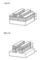
- FIG. 2is a perspective view showing that a photoresist for forming a metal line is coated on a wafer during a seasoning process according to an exemplary embodiment of the present invention.
- FIG. 3A to FIG. 3Dare cross-sectional views showing sequential states of a method of performing a seasoning process for a semiconductor device according to an exemplary embodiment of the present invention.
- FIG. 2is a perspective view showing that a photoresist for forming a metal line is coated on a wafer during a seasoning process according to an exemplary embodiment of the present invention.
- the photoresist 110is not coated or patterned on an entire surface of a wafer, but rather is coated in a ring shape such that a central region of the wafer is exposed (or opened) and an edge region of the wafer is covered (or closed).
- the semiconductor device processing chamber or apparatus seasoned by the present inventioncomprises an etching chamber or apparatus, preferably a dry (or plasma) etching chamber or apparatus.
- etching chamber or apparatuspreferably a dry (or plasma) etching chamber or apparatus.
- each photoresist pattern portion 110generally has a ring shape, such as a circular, rectangular, or polygonal shape.
- reference numeral 100denotes an insulating layer on a semiconductor substrate (e.g., a test wafer), and reference numeral 106 denotes a metal layer for a metal line or anti-reflection coating layer.
- the metal layer or anti-reflection coating layeris the material layer to be etched in the present seasoning process.
- the insulating layer 100may be located between two metal layers, in which case it can be considered to be an interlayer insulating layer.
- a photoresist patternis not formed on the entire surface of a test wafer, but rather is formed in predetermined regions of the test wafer, such as the edge region, and not in a central region of the test wafer. Accordingly, when dry-etching is performed using the test wafer photoresist pattern, the etch residue may be uniformly accumulated on the wafer, and the total amount of etch residue in the etch chamber may decrease.
- FIG. 3A to FIG. 3Dare cross-sectional views showing sequential stages of a method of performing a seasoning process according to an exemplary embodiment of the present invention.
- an anti-reflection coating layer 102 , a metal layer 104 , and an anti-reflection coating layer 106are sequentially deposited or formed on an insulating layer 100 to form a (patternable) structure in a semiconductor substrate.
- the insulating layercomprises an insulating material, such as USG, BSG, PSG, BPSG, etc., and the thickness of the interlayer insulating layer may be 3000 ⁇ or more.
- the anti-reflection coating layers 102 and 106may comprise a metal material, such as Ti, TiN, or a metal alloy material such as TiW alloy, and the thickness of each anti-reflection coating layer may be 1.3 ⁇ m or more.
- the metal layer 104comprises a metal material, such as Al, Al—Cu alloy or Cu.
- the anti-reflection coating layer 102 , the metal layer 104 , and the anti-reflection coating layer 106are formed on a test wafer by performing the same manufacturing process as that of an actual running wafer.
- the photoresist 110when the photoresist 110 is coated on an upper part of the anti-reflection coating 106 on the test wafer, the photoresist 110 is patterned not on the entire surface of the upper part of the anti-reflection coating 106 , but rather in concentric ring shapes, and such that a central region of the anti-reflection coating 106 is opened or exposed and an edge region of the anti-reflection coating 106 is covered or closed.
- several photoresist rings 110are formed in a predetermined gap between the central region and the edge region of the wafer.
- the photoresist 110may be located on the outermost 1 cm or more of the edge of the wafer (e.g., the outermost 1 cm, 2 cm, 3 cm, 5 cm, etc.). Also, the innermost 5 cm, 10 cm, 20 cm, 25 cm, or 50 cm, etc. (i.e., a region within a 2.5 cm, 5 cm, 10 cm, 12.5 cm, or 25 cm radius of the center) of the test wafer may have no photoresist thereon, as may be desired or determined empirically or in accordance with certain design or manufacturing considerations.
- a pattern to define a metal line regionis formed when the ring-shaped photoresist 110 on the test wafer is exposed to photolithographic radiation and developed using a metal line mask.
- metal interconnection linesare formed by dry-etching the anti-reflection coating layer 106 , the metal layer 104 , and the anti-reflection coating layer 102 using the photoresist pattern 110 as an etch mask.
- the anti-reflection coating 106 , the metal layer 104 , and the anti-reflection coating 102are dry-etched to an end point (e.g., to a degree such that the insulating layer 100 is exposed).
- the reactive ion etchingis performed under conditions in which a pressure in a dry-etching chamber may be about 8 mTorr, a source power may be about 9000 W, a bias power may be about 200 W or above, Cl 2 gas is supplied at a flow rate of about 50 sccm, BCl 3 gas is supplied at a flow rate of about 25 sccm, and CHF 3 gas is supplied at a flow rate of about 10 sccm.
- the anti-reflection coating 106 , the metal layer 104 , and the anti-reflection coating 102may be etched in a 50% overcut etch profile under conditions in which a pressure in the dry-etching chamber may be about 8 mTorr, the source power may be about 9000 W, the bias power may be about 100 W or less, BCl 3 gas is supplied at a flow rate of about 25 sccm, CHP 3 gas is supplied at a flow rate of about 25 sccm, and Ar gas is supplied at a flow rate of about 50 sccm.
- a pressure in the dry-etching chambermay be about 8 mTorr
- the source powermay be about 9000 W
- the bias powermay be about 100 W or less
- BCl 3 gasis supplied at a flow rate of about 25 sccm
- CHP 3 gasis supplied at a flow rate of about 25 sccm
- Ar gasis supplied at a flow rate of about 50 sccm.
- an etching residuesuch as of the ring-shaped photoresist pattern 110 , polymers, etc.
- the ashing processesmay be performed under the following three process conditions.
- a first set of ashing process conditionsmay include a pressure in the chamber of about 2 Torr, a power of about 1400 W, O 2 gas supplied at a flow rate of about 3000 sccm, N 2 gas supplied at a flow rate of about 300 sccm, a processing time of about 50 seconds, and a process temperature of about 250° C.
- a second set of ashing process conditionsmay include a pressure in the chamber of about 2 Torr, a power of about 1400 W, H 2 O gas supplied at a flow rate of about 750 sccm, CF 4 gas supplied at a flow rate of about 75 sccm, a processing time of about 20 seconds, and a process temperature of about 250° C.
- a third set of ashing process conditionsmay include a pressure in the chamber of about 2 Torr, a power of about 1400 W, O 2 gas supplied at a flow rate of about 3000 sccm, a processing time of about 205 seconds, and a process temperature of about 250° C.
- An etch residue on the test wafer, including the ring-shaped photoresist pattern 110 , polymer, etc.,may be removed under such ashing process conditions.
- the total amount of etch residuemay be reduced since the etch residue may uniformly occur over the entire wafer, since the photoresist is patterned depending on whether it is in a central region or an edge region of the wafer. That is, the photoresist that is a main source of the etch residue at the central region is not on the central region of the wafer, but it is on the edge region thereof so as to cover or close the anti-reflection coating layer or metal layer that is a main source of the etch residue at the edge portion. Therefore, the etch residue in total may become uniform throughout the central and edge regions of the wafer and/or the total amount of etch residue may be reduced.
- the dry-etching processis performed after patterning the photoresist in a ring shape so as to open or expose the central region of the test wafer (and thus remove the photoresist that may be a primary source of etch residue or particles in such region) and to close or cover the edge region thereof (and thus protect against etching the antireflective coating and/or metal that may be a primary source of etch residue or particles in such region), the etch residue may be uniformly accumulated on the central region of the wafer and edge region of the wafer, and the total amount of etch residue may decrease. Consequently, test and/or production yield(s) of a semiconductor device may be improved.
Landscapes
- Engineering & Computer Science (AREA)
- Physics & Mathematics (AREA)
- Condensed Matter Physics & Semiconductors (AREA)
- General Physics & Mathematics (AREA)
- Manufacturing & Machinery (AREA)
- Computer Hardware Design (AREA)
- Microelectronics & Electronic Packaging (AREA)
- Power Engineering (AREA)
- Plasma & Fusion (AREA)
- Drying Of Semiconductors (AREA)
Abstract
Description
Claims (20)
Applications Claiming Priority (2)
| Application Number | Priority Date | Filing Date | Title |
|---|---|---|---|
| KR10-2004-0113250 | 2004-12-27 | ||
| KR1020040113250AKR100688776B1 (en) | 2004-12-27 | 2004-12-27 | Seasoning method of semiconductor device |
Publications (2)
| Publication Number | Publication Date |
|---|---|
| US20060141798A1 US20060141798A1 (en) | 2006-06-29 |
| US7297607B2true US7297607B2 (en) | 2007-11-20 |
Family
ID=36612308
Family Applications (1)
| Application Number | Title | Priority Date | Filing Date |
|---|---|---|---|
| US11/303,891Expired - Fee RelatedUS7297607B2 (en) | 2004-12-27 | 2005-12-15 | Device and method of performing a seasoning process for a semiconductor device manufacturing apparatus |
Country Status (2)
| Country | Link |
|---|---|
| US (1) | US7297607B2 (en) |
| KR (1) | KR100688776B1 (en) |
Cited By (1)
| Publication number | Priority date | Publication date | Assignee | Title |
|---|---|---|---|---|
| US20110295554A1 (en)* | 2010-05-26 | 2011-12-01 | Samsung Electronics Co., Ltd. | Equipment For Manufacturing Semiconductor Device And Seasoning Process Method Of The Same |
Families Citing this family (5)
| Publication number | Priority date | Publication date | Assignee | Title |
|---|---|---|---|---|
| KR100595330B1 (en)* | 2005-06-02 | 2006-07-03 | 동부일렉트로닉스 주식회사 | Metal wiring formation method of semiconductor device |
| KR100859640B1 (en)* | 2006-12-26 | 2008-09-23 | 동부일렉트로닉스 주식회사 | Method for manufacturing test wafer for sining process of semiconductor manufacturing apparatus |
| US9304283B2 (en)* | 2014-05-22 | 2016-04-05 | Texas Instruments Incorporated | Bond-pad integration scheme for improved moisture barrier and electrical contact |
| US9953886B2 (en) | 2015-08-21 | 2018-04-24 | Microchip Technology Incorporated | Single-wafer real-time etch rate and uniformity predictor for plasma etch processes |
| CN116884884B (en)* | 2023-09-06 | 2023-11-24 | 粤芯半导体技术股份有限公司 | Warming-up sheet for grid side wall ICP etching, preparation method thereof and warming-up method |
Citations (4)
| Publication number | Priority date | Publication date | Assignee | Title |
|---|---|---|---|---|
| US4586243A (en)* | 1983-01-14 | 1986-05-06 | General Motors Corporation | Method for more uniformly spacing features in a semiconductor monolithic integrated circuit |
| US20020173149A1 (en)* | 2001-05-18 | 2002-11-21 | Speedfam Co., Ltd. | Local dry etching method |
| US20030183920A1 (en)* | 2002-03-28 | 2003-10-02 | Goodrich Joel Lee | Hermetic electric component package |
| US6890834B2 (en)* | 2001-06-11 | 2005-05-10 | Matsushita Electric Industrial Co., Ltd. | Electronic device and method for manufacturing the same |
Family Cites Families (4)
| Publication number | Priority date | Publication date | Assignee | Title |
|---|---|---|---|---|
| KR20010005085A (en)* | 1999-06-30 | 2001-01-15 | 김영환 | A method for fabricating semiconductor device |
| US6455333B1 (en)* | 2001-02-28 | 2002-09-24 | Advanced Micro Devices, Inc. | Method of achieving stable deep ultraviolet (DUV) resist etch rate for gate critical dimension (CD) |
| KR100418121B1 (en)* | 2001-12-22 | 2004-02-14 | 동부전자 주식회사 | Method For Fabricating Semiconductor Devices |
| KR20050045393A (en)* | 2003-11-11 | 2005-05-17 | 주식회사 하이닉스반도체 | Method of manufacturing a semiconductor device |
- 2004
- 2004-12-27KRKR1020040113250Apatent/KR100688776B1/ennot_activeExpired - Fee Related
- 2005
- 2005-12-15USUS11/303,891patent/US7297607B2/ennot_activeExpired - Fee Related
Patent Citations (6)
| Publication number | Priority date | Publication date | Assignee | Title |
|---|---|---|---|---|
| US4586243A (en)* | 1983-01-14 | 1986-05-06 | General Motors Corporation | Method for more uniformly spacing features in a semiconductor monolithic integrated circuit |
| US20020173149A1 (en)* | 2001-05-18 | 2002-11-21 | Speedfam Co., Ltd. | Local dry etching method |
| US6890834B2 (en)* | 2001-06-11 | 2005-05-10 | Matsushita Electric Industrial Co., Ltd. | Electronic device and method for manufacturing the same |
| US6965107B2 (en)* | 2001-06-11 | 2005-11-15 | Matsushita Electric Industrial Co., Ltd. | Semiconductor-based encapsulated infrared sensor and electronic device |
| US20030183920A1 (en)* | 2002-03-28 | 2003-10-02 | Goodrich Joel Lee | Hermetic electric component package |
| US7026223B2 (en)* | 2002-03-28 | 2006-04-11 | M/A-Com, Inc | Hermetic electric component package |
Cited By (2)
| Publication number | Priority date | Publication date | Assignee | Title |
|---|---|---|---|---|
| US20110295554A1 (en)* | 2010-05-26 | 2011-12-01 | Samsung Electronics Co., Ltd. | Equipment For Manufacturing Semiconductor Device And Seasoning Process Method Of The Same |
| US9136138B2 (en)* | 2010-05-26 | 2015-09-15 | Samsung Electronics Co., Ltd. | Equipment for manufacturing semiconductor device and seasoning process method of the same |
Also Published As
| Publication number | Publication date |
|---|---|
| US20060141798A1 (en) | 2006-06-29 |
| KR20060074497A (en) | 2006-07-03 |
| KR100688776B1 (en) | 2007-03-02 |
Similar Documents
| Publication | Publication Date | Title |
|---|---|---|
| US7183198B2 (en) | Method for forming a hardmask employing multiple independently formed layers of a capping material to reduce pinholes | |
| JP3957319B2 (en) | Method for etching a semiconductor wafer | |
| US6291137B1 (en) | Sidewall formation for sidewall patterning of sub 100 nm structures | |
| US7482279B2 (en) | Method for fabricating semiconductor device using ArF photolithography capable of protecting tapered profile of hard mask | |
| US5932487A (en) | Method for forming a planar intermetal dielectric layer | |
| US6268287B1 (en) | Polymerless metal hard mask etching | |
| US11329218B2 (en) | Multiply spin-coated ultra-thick hybrid hard mask for sub 60nm MRAM devices | |
| US6103457A (en) | Method for reducing faceting on a photoresist layer during an etch process | |
| US7115524B2 (en) | Methods of processing a semiconductor substrate | |
| US20090117744A1 (en) | Ion implantation mask forming method | |
| US7297607B2 (en) | Device and method of performing a seasoning process for a semiconductor device manufacturing apparatus | |
| US20050181604A1 (en) | Method for structuring metal by means of a carbon mask | |
| US20070161255A1 (en) | Method for etching with hardmask | |
| KR100843899B1 (en) | Manufacturing method of semiconductor device | |
| US6797628B2 (en) | Methods of forming integrated circuitry, semiconductor processing methods, and processing method of forming MRAM circuitry | |
| US6133145A (en) | Method to increase the etch rate selectivity between metal and photoresist via use of a plasma treatment | |
| US6569760B1 (en) | Method to prevent poison via | |
| US7538025B2 (en) | Dual damascene process flow for porous low-k materials | |
| US6613680B2 (en) | Method of manufacturing a semiconductor device | |
| JP3358547B2 (en) | Wiring formation method | |
| US6287752B1 (en) | Semiconductor device, method of manufacturing a semiconductor device, and method of forming a pattern for semiconductor device | |
| US6451706B1 (en) | Attenuation of reflecting lights by surface treatment | |
| KR100807521B1 (en) | Semiconductor device manufacturing method | |
| US20080124914A1 (en) | Method of fabricating flash memory device | |
| US6548231B1 (en) | Enhanced passivation scheme for post metal etch clean process |
Legal Events
| Date | Code | Title | Description |
|---|---|---|---|
| AS | Assignment | Owner name:DONGBUANAM SEMICONDUCTOR INC., KOREA, REPUBLIC OF Free format text:ASSIGNMENT OF ASSIGNORS INTEREST;ASSIGNOR:JO, BO-YEOUN;REEL/FRAME:017349/0056 Effective date:20051215 | |
| AS | Assignment | Owner name:DONGBU ELECTRONICS CO., LTD.,KOREA, REPUBLIC OF Free format text:CHANGE OF NAME;ASSIGNOR:DONGANAM SEMICONDUCTOR INC.;REEL/FRAME:017749/0335 Effective date:20060328 Owner name:DONGBU ELECTRONICS CO., LTD., KOREA, REPUBLIC OF Free format text:CHANGE OF NAME;ASSIGNOR:DONGANAM SEMICONDUCTOR INC.;REEL/FRAME:017749/0335 Effective date:20060328 | |
| AS | Assignment | Owner name:DONGBU ELECTRONICS CO., LTD., KOREA, REPUBLIC OF Free format text:CORRECTIVE ASSIGNMENT TO CORRECT THE ASSIGNOR PREVIOUSLY RECORDED ON REEL 017749 FRAME 0335;ASSIGNOR:DONGBUANAM SEMICONDUCTOR INC.;REEL/FRAME:017821/0670 Effective date:20060328 Owner name:DONGBU ELECTRONICS CO., LTD.,KOREA, REPUBLIC OF Free format text:CORRECTIVE ASSIGNMENT TO CORRECT THE ASSIGNOR PREVIOUSLY RECORDED ON REEL 017749 FRAME 0335. ASSIGNOR(S) HEREBY CONFIRMS THE ASSIGNOR SHOULD BE "DONGBUANAM SEMICONDUCTOR INC.";ASSIGNOR:DONGBUANAM SEMICONDUCTOR INC.;REEL/FRAME:017821/0670 Effective date:20060328 Owner name:DONGBU ELECTRONICS CO., LTD., KOREA, REPUBLIC OF Free format text:CORRECTIVE ASSIGNMENT TO CORRECT THE ASSIGNOR PREVIOUSLY RECORDED ON REEL 017749 FRAME 0335. ASSIGNOR(S) HEREBY CONFIRMS THE ASSIGNOR SHOULD BE "DONGBUANAM SEMICONDUCTOR INC.";ASSIGNOR:DONGBUANAM SEMICONDUCTOR INC.;REEL/FRAME:017821/0670 Effective date:20060328 | |
| FEPP | Fee payment procedure | Free format text:PAYOR NUMBER ASSIGNED (ORIGINAL EVENT CODE: ASPN); ENTITY STATUS OF PATENT OWNER: LARGE ENTITY | |
| FEPP | Fee payment procedure | Free format text:PAYER NUMBER DE-ASSIGNED (ORIGINAL EVENT CODE: RMPN); ENTITY STATUS OF PATENT OWNER: LARGE ENTITY Free format text:PAYOR NUMBER ASSIGNED (ORIGINAL EVENT CODE: ASPN); ENTITY STATUS OF PATENT OWNER: LARGE ENTITY | |
| FPAY | Fee payment | Year of fee payment:4 | |
| REMI | Maintenance fee reminder mailed | ||
| LAPS | Lapse for failure to pay maintenance fees | ||
| STCH | Information on status: patent discontinuation | Free format text:PATENT EXPIRED DUE TO NONPAYMENT OF MAINTENANCE FEES UNDER 37 CFR 1.362 | |
| FP | Lapsed due to failure to pay maintenance fee | Effective date:20151120 |