US7295475B2 - Flash memory programming using an indication bit to interpret state - Google Patents
Flash memory programming using an indication bit to interpret stateDownload PDFInfo
- Publication number
- US7295475B2 US7295475B2US11/229,664US22966405AUS7295475B2US 7295475 B2US7295475 B2US 7295475B2US 22966405 AUS22966405 AUS 22966405AUS 7295475 B2US7295475 B2US 7295475B2
- Authority
- US
- United States
- Prior art keywords
- memory cells
- bits
- memory
- programmed
- logic
- Prior art date
- Legal status (The legal status is an assumption and is not a legal conclusion. Google has not performed a legal analysis and makes no representation as to the accuracy of the status listed.)
- Active, expires
Links
- 230000015654memoryEffects0.000titleclaimsabstractdescription163
- 238000000034methodMethods0.000claimsabstractdescription19
- 239000004065semiconductorSubstances0.000claimsdescription6
- 229910052710siliconInorganic materials0.000claimsdescription5
- 239000010703siliconSubstances0.000claimsdescription5
- 239000010410layerSubstances0.000description34
- 238000010586diagramMethods0.000description10
- VYPSYNLAJGMNEJ-UHFFFAOYSA-NSilicium dioxideChemical compoundO=[Si]=OVYPSYNLAJGMNEJ-UHFFFAOYSA-N0.000description5
- 238000003491arrayMethods0.000description5
- 230000006870functionEffects0.000description4
- 230000002093peripheral effectEffects0.000description4
- 239000000758substrateSubstances0.000description4
- 230000003213activating effectEffects0.000description3
- PNEYBMLMFCGWSK-UHFFFAOYSA-Naluminium oxideInorganic materials[O-2].[O-2].[O-2].[Al+3].[Al+3]PNEYBMLMFCGWSK-UHFFFAOYSA-N0.000description3
- 229910052814silicon oxideInorganic materials0.000description3
- 230000005684electric fieldEffects0.000description2
- 239000002784hot electronSubstances0.000description2
- 239000012535impuritySubstances0.000description2
- 238000002347injectionMethods0.000description2
- 239000007924injectionSubstances0.000description2
- 150000004767nitridesChemical class0.000description2
- ZOXJGFHDIHLPTG-UHFFFAOYSA-NBoronChemical compound[B]ZOXJGFHDIHLPTG-UHFFFAOYSA-N0.000description1
- OAICVXFJPJFONN-UHFFFAOYSA-NPhosphorusChemical compound[P]OAICVXFJPJFONN-UHFFFAOYSA-N0.000description1
- 229910052581Si3N4Inorganic materials0.000description1
- XUIMIQQOPSSXEZ-UHFFFAOYSA-NSiliconChemical compound[Si]XUIMIQQOPSSXEZ-UHFFFAOYSA-N0.000description1
- 229910000577Silicon-germaniumInorganic materials0.000description1
- LEVVHYCKPQWKOP-UHFFFAOYSA-N[Si].[Ge]Chemical compound[Si].[Ge]LEVVHYCKPQWKOP-UHFFFAOYSA-N0.000description1
- 230000004913activationEffects0.000description1
- 229910052785arsenicInorganic materials0.000description1
- RQNWIZPPADIBDY-UHFFFAOYSA-Narsenic atomChemical compound[As]RQNWIZPPADIBDY-UHFFFAOYSA-N0.000description1
- 229910052796boronInorganic materials0.000description1
- 230000003139buffering effectEffects0.000description1
- 230000001413cellular effectEffects0.000description1
- 229910052681coesiteInorganic materials0.000description1
- 229910052593corundumInorganic materials0.000description1
- 229910052906cristobaliteInorganic materials0.000description1
- 230000001419dependent effectEffects0.000description1
- 239000003989dielectric materialSubstances0.000description1
- 230000000694effectsEffects0.000description1
- 229910052732germaniumInorganic materials0.000description1
- GNPVGFCGXDBREM-UHFFFAOYSA-Ngermanium atomChemical compound[Ge]GNPVGFCGXDBREM-UHFFFAOYSA-N0.000description1
- 238000012986modificationMethods0.000description1
- 230000004048modificationEffects0.000description1
- 229910052698phosphorusInorganic materials0.000description1
- 239000011574phosphorusSubstances0.000description1
- 229910021420polycrystalline siliconInorganic materials0.000description1
- 229920005591polysiliconPolymers0.000description1
- 238000005036potential barrierMethods0.000description1
- 230000008569processEffects0.000description1
- 239000000377silicon dioxideSubstances0.000description1
- HQVNEWCFYHHQES-UHFFFAOYSA-Nsilicon nitrideChemical compoundN12[Si]34N5[Si]62N3[Si]51N64HQVNEWCFYHHQES-UHFFFAOYSA-N0.000description1
- 239000002356single layerSubstances0.000description1
- 230000003068static effectEffects0.000description1
- 229910052682stishoviteInorganic materials0.000description1
- 229910052905tridymiteInorganic materials0.000description1
- 229910001845yogo sapphireInorganic materials0.000description1
Images


Classifications
- G—PHYSICS
- G11—INFORMATION STORAGE
- G11C—STATIC STORES
- G11C16/00—Erasable programmable read-only memories
- G11C16/02—Erasable programmable read-only memories electrically programmable
- G11C16/04—Erasable programmable read-only memories electrically programmable using variable threshold transistors, e.g. FAMOS
- G11C16/0491—Virtual ground arrays
- G—PHYSICS
- G11—INFORMATION STORAGE
- G11C—STATIC STORES
- G11C16/00—Erasable programmable read-only memories
- G11C16/02—Erasable programmable read-only memories electrically programmable
- G11C16/04—Erasable programmable read-only memories electrically programmable using variable threshold transistors, e.g. FAMOS
- G11C16/0466—Erasable programmable read-only memories electrically programmable using variable threshold transistors, e.g. FAMOS comprising cells with charge storage in an insulating layer, e.g. metal-nitride-oxide-silicon [MNOS], silicon-oxide-nitride-oxide-silicon [SONOS]
- G11C16/0475—Erasable programmable read-only memories electrically programmable using variable threshold transistors, e.g. FAMOS comprising cells with charge storage in an insulating layer, e.g. metal-nitride-oxide-silicon [MNOS], silicon-oxide-nitride-oxide-silicon [SONOS] comprising two or more independent storage sites which store independent data
- G—PHYSICS
- G11—INFORMATION STORAGE
- G11C—STATIC STORES
- G11C16/00—Erasable programmable read-only memories
- G11C16/02—Erasable programmable read-only memories electrically programmable
- G11C16/06—Auxiliary circuits, e.g. for writing into memory
- G11C16/10—Programming or data input circuits
Definitions
- the present inventionrelates generally to non-volatile memory devices, and more specifically, to data programming operations for non-volatile memory devices.
- Flash memoryis a common type of non-volatile semiconductor memory device. Non-volatile refers to the trait of retaining stored data when power is turned off. Because Flash memory is non-volatile, it is commonly used in power conscious applications, such as in battery powered cellular phones, personal digital assistants (PDAs), and in portable mass storage devices such as memory sticks.
- PDAspersonal digital assistants
- Flash memory devicestypically include multiple individual components formed on or within a substrate. Such devices often comprise a high density section and a low density section.
- a Flash memorymay include one or more high density core regions and a low density peripheral portion formed on a single substrate.
- the high density core regionstypically include arrays of individually addressable, substantially identical memory cells.
- the low density peripheral portionmay include input/output (I/O) circuitry, circuitry for selectively addressing the individual cells (such as decoders for connecting the source, gate and drain of selected cells to predetermined voltages or impedances to effect designated operations of the cell such as programming, reading or erasing), and voltage regulation and supply circuitry.
- I/Oinput/output
- Flash memory architectureIn one particular type of Flash memory architecture, called NOR Flash memory, memory cells within the core portion are coupled together in a circuit configuration in which each memory cell has a drain, a source, and a stacked gate. In operation, memory cells may be addressed by circuitry in the peripheral portion to perform functions such as reading, erasing, and programming of the memory cells.
- power supply circuitrymay be used to supply a current to each memory cell (bit) that is to be programmed. Since each circuit that is being programmed may source a fixed amount of current, a limited number of memory cells can be programmed before exhausting the capacity of power supply circuitry.
- One aspectis directed to a non-volatile memory device comprising an array of non-volatile memory cells that includes a plurality of groups of memory cells and a plurality of memory cells used to respectively indicate whether a programmed/non-programmed state of the memory cells in one of the groups is interpreted as a logic zero or a logic one.
- Another aspectis directed to a method for writing data to memory cells of a non-volatile memory device.
- the methodincludes receiving a predetermined number of bits that are to be written and analyzing the predetermined number of bits to determine a logic state of a minority of the bits.
- the methodfurther includes writing each of the bits to a memory cell in the memory device by programming those that correspond to the minority of the bits and writing an indication bit that indicates the determined logic state of the minority of the bits.
- FIG. 1is a block diagram illustrating an exemplary high-level implementation of a memory device
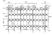
- FIG. 2is a diagram illustrating an exemplary portion of an array of memory cells implemented in the core area of the memory device shown in FIG. 1 ;
- FIGS. 3 and 4are diagrams illustrating a cross-section of an exemplary one of the memory cells shown in FIG. 2 ;
- FIG. 5is a diagram illustrating a programming window for the memory device of FIG. 1 ;
- FIG. 6is a flow chart illustrating exemplary operations for writing multiple bits to the core area shown in FIG. 1 ;
- FIG. 7is a diagram illustrating an exemplary simplified programming window.
- Flash memory programming techniquethat dynamically selects how the programmed or non-programmed state of a Flash memory cell is to be interpreted.
- a special “indication bit”may be used to indicate the selection.
- FIG. 1is a block diagram illustrating an exemplary high-level implementation of a memory device 100 .
- Memory device 100may be a Flash memory device implemented as an integrated circuit.
- memory device 100includes a core area 102 .
- Core area 102may include arrays of high density memory cells, such as, for example, SONOS-type (silicon-oxide-nitride-oxide-silicon) NOR memory cells, where the nitride layer acts as the charge storage element. More specifically, core area 102 may include multiple M ⁇ N memory arrays of substantially identical memory cells.
- the memory cells in area 102may be implemented such that each memory cell can store two or more bits.
- each memory cellcan store two or more bits.
- MirrorBitTMmulti-bit per memory cell technology
- the intrinsic density of a Flash memory arraycan be doubled by storing two physically distinct charges on opposite sides of a memory cell.
- Each charge, representing a bit within a cellserves as a binary unit of data (e.g. either “1” or “0”). Reading or programming one side of a memory cell occurs independently of the data that is stored on the opposite side of the cell.
- core area 102may be implemented as a number of memory cell arrays. Each such memory cell array may be associated with X-decoder 110 and Y-decoder 108 .
- X-decoder 110 and Y-decoder 108may decode address information, such as addresses received by memory device 100 that define a specific byte or word (or groups of bytes or words) that are to be written to or read from. The decoded addresses specify the appropriate physical lines in the memory cell array(s) that are to be used.
- Y-decoder 108may also include appropriate sense amplifier circuitry. Sense amplifiers may be used to sense the programmed or non-programmed state of the memory cells in core area 102 .
- Random access memory (RAM) 104may include memory, such as static dynamic random access memory (SRAM) or dynamic random access memory (DRAM) type memory, that can serve as a memory cache between core area 102 and I/O lines/pins 114 . Relative to the memory cells in core area 102 , RAM 104 may be a higher speed memory and may be a volatile memory (i.e., loses its data when powered down). I/O lines 114 may provide buffering to facilitate data transfer between RAM 104 or between core area 102 and external circuitry.
- SRAMstatic dynamic random access memory
- DRAMdynamic random access memory
- Voltage supply generator 112may act as a power supply for the programming, reading, and erasing functions performed on the memory cells in core area 102 . Programming and erasing the memory cells, in particular, may require supply voltages larger than those supplied to memory device 100 . For example, memory device 100 may be powered from a 3.5 volt source while a program operation may require a higher voltage source. Voltage supply generator 112 may use one or more charge pumps to generate these higher voltages. Consistent with an aspect of the invention and as described in more detail below, voltage supply generator 112 may include a charge pump divided into groups of independent charge pumps.
- Control logic 106may generally control Y-decoder 108 , X-decoder 110 , RAM 104 , voltage supply generator 112 , and I/O lines 114 to control the reading, programming, and erasing of memory cell core area 102 .
- Control logic 106may include a state machine that appropriately manipulates memory cell core area 102 based on input address, data, and control signals received by memory device 100 through I/O lines 114 .
- FIG. 2is a diagram illustrating an exemplary portion of an array of memory cells implemented in core area 102 , labeled as memory array 210 .
- the arrayincludes a number of substantially identical memory cells 201 .
- Each memory cell 201includes a drain 202 , a source 203 , and a stacked gate region 204 .
- Drain 202 and source 203are interchangeable within a memory cell depending on the applied voltages and may be switched with respect to one another.
- the NOR configuration illustrated in FIG. 2includes word lines (word lines WL 1 through WL N ) each connected to the gate region 204 of a number of memory cells 201 in a row. Bit lines are arranged orthogonally to the word lines in array 210 .
- the bit linesinclude global bit lines (GBL i ⁇ 1 through GBL i+2 ) that each connect to one or more additional bit lines 215 . Voltages placed on additional bit lines 215 via a global bit line GBL may be controlled through select transistors (also called select switches) S 0 through S 7 .
- select transistors S 0 through S 7may be arranged in repeating groups 225 of select transistors. Corresponding select transistors in a number of groups may be controlled by the same control signal. For example, activating select transistor S 0 may connect the particular bit line connected to S 0 to voltages applied to GBL i , GBL i+2 , etc. If select transistor S 1 was also activated, GBL i+1 , GBL i+3 , etc., would also be connected to the opposing source/drain of a number of memory cells 201 in memory array 210 .
- one memory cell in each group 225may have its source, drain, and gate terminals all activated, thus allowing programming and reading of this select memory cell.
- a particular memory cell within a group 225e.g., the memory cell within the dashed circle in FIG. 2
- this cellhas voltages applied to its gate, source, and drain and may be programmed or read.
- Other memory cells 201 in other groups 225can be simultaneously selected based on activation of the same WL and select transistors.
- memory cells 201 in core area 102are shown as NOR memory cells, in some implementations, the circuitry in the peripheral regions of memory device 100 may provide an external interface that mimics an external interface normally provided by NAND-type Flash memories. In this situation, memory device 100 , from the point of view of the user/circuit designer, can effectively be thought of as a NAND-type Flash device even though core area 102 includes NOR-type Flash memory.
- core array 102may include multiple memory cell arrays, each including 2048 bit lines and 256 word lines.
- the 2048 bit linesmay correspond to 256 eight memory cell groups 225 of select transistors.
- FIG. 3is a diagram illustrating a cross-section of an exemplary one of memory cells 201 in more detail.
- Memory cell 201may be formed on a substrate 310 and includes drain 202 , source 203 , and stacked gate 204 .
- Substrate 310may be formed of a semiconducting material such as silicon, germanium, or silicon-germanium.
- Drain and source regions 202 and 203may be regions that are doped with n-type impurities, such as phosphorus or arsenic, or p-type impurities, such as boron. As previously mentioned, depending on the applied voltages, the functions of drain and source regions 202 and 203 may be reversed.
- stacked gate 204is formed on channel region 315 .
- Stacked gate 204includes a number of layers, including a relatively thin gate dielectric layer 320 , a charge storage layer 322 , a second dielectric layer 324 , and a control gate 328 .
- Dielectric layer 320may include an oxide, such as a silicon oxide (e.g., SiO 2 ).
- Charge storage layer 322may be formed on gate dielectric layer 320 and may include a dielectric material, such as a nitride (e.g., a silicon nitride). Layer 322 acts as a charge storage layer for the memory cell.
- a dielectric materialsuch as a nitride (e.g., a silicon nitride). Layer 322 acts as a charge storage layer for the memory cell.
- Charge storage layer 322may be used to store one or more bits of information.
- charge storage layer 322may store charges representing two separate bits of data by localizing the first and second charges to the respective left and right sides of charge storage layer 322 .
- Each of the two charges of the memory cell 201may be programmed independently by, for example, channel hot electron injection, to store a charge on each respective side of the charge storage layer 322 .
- the charges in charge storage layer 322become effectively trapped on each respective side of charge storage layer 322 and the density of the resulting memory array may be increased as compared to memory devices that store only one bit of data per cell.
- charge storage layer 322may store charges representing three or more bits of data for each memory cell 201 .
- Second dielectric layer 324may be formed on layer 322 and may include a multi-layer structure, such as a first silicon oxide layer 325 and a second high dielectric constant (high-K) layer 326 .
- High-K layer 326may include, for example, an alumina, such as Al 2 O 3 .
- Dielectric layers 325 and 326may together function as an inter-gate dielectric for memory cells 201 .
- dielectric layer 324may include a single layer, such as a silicon oxide or alumina.
- Control gate 328may be formed above second dielectric layer 324 .
- Control gate 328may be formed of polysilicon and may be connected to the word line of memory cell 201 .
- core area 102 of memory device 100may be programmed by a channel hot electron injection process that injects electrons into charge storage layer 322 .
- the injected electronsbecome trapped in charge storage layer 322 until an erase operation is performed.
- memory cells 201 in core array 102may be programmed by applying a relatively high voltage (e.g., 9 volts) to one of the word lines WL, such as WL 1 , which effectively applies the voltage to control gates 328 of the memory cells that are coupled to WL 1 .
- a voltagemay be applied across drain 202 and source 203 of one of the memory cells in a group 215 . For example, approximately five volts may be applied to GBL i and GBL i+1 may be grounded.
- select transistors S 0 and S 1may be turned on. These voltages generate a vertical and lateral electric field in the activated memory cell(s) (e.g., the circled memory cell in FIG.
- the source and drain terminalsare interchanged.
- the corresponding read operationmay be performed by applying approximately three volts to WL 1 , grounding GBL i , and applying approximately 1.5 volts to GBL i+1 .
- FIG. 4is a diagram similar to FIG. 3 . Additionally, FIG. 4 illustrates read and program directions for when memory cell 201 is used to store charges representing two independent bits.
- Memory cell 201includes two separate charge storage areas 432 and 434 within charge storage layer 322 . Each storage area 432 and 434 may define one bit.
- area 203acts as the drain and receives a high voltage relative to area 202 , which acts as the source.
- area 202acts as the drain and receives a high voltage relative to area 203 , which acts as the source.
- the arrows in FIG. 4graphically illustrate the direction of charge flow.
- Multiple memory cells 201 in a rowcan be simultaneously programmed by activating a programming voltage differential through the global bit lines and select switches S 0 through S 7 to the source and drain of each memory cell 201 that is to be programmed.
- Voltage supply generator 112may provide this program voltage.
- memory cells 201may be programmed in discrete programming “windows,” in which each window includes, for example, 64 bits.
- Programming window 515may include a certain number of bits (e.g., 256 in this example) that are to be written to memory cell core area 102 and may be mapped to 256 bit lines 510 in core area 102 . Based on each of the bits in programming window 515 , a corresponding bit line 510 will be either activated or not activated via the global bit lines and select transistors S 0 through S 7 (not shown in FIG. 5 ) to provide current on the activated drain bit lines from voltage supply generator 112 . Programming window 515 may be further subdivided into sub-windows 520 , such as by subdividing the 256 bits in programming window 515 into four 64-bit windows 520 . In one implementation, sub-windows 520 may be programmed sequentially relative to one another. In this implementation, when sub-windows 520 are 64-bit windows, then each programming window 520 may simultaneously write 64 bits to core area 102 during a programming cycle.
- sub-windows 520may simultaneously write 64 bits to core area
- the program window sizeis described as being 64 bits wide. That is, programming is performed in 64-bit chunks.
- One of ordinary skill in the artwill recognize that other program window sizes could be used.
- Programming a memory cellrefers to the application of voltages, as previously described, to the drain, source, and word lines of a memory cell such that charge is injected into charge storage layer 322 .
- Writing a bitmay involve either programming a memory cell or not programming a memory cell, depending on the desired state of the memory cell. For example, if the programmed state of a memory cell is interpreted as a logic one, and a logic one is to be written to a memory cell, then the logic one bit is written by programming the memory cell. However, if the programmed state of a memory cell is interpreted as a logic one, and a logic zero is to be written to a memory cell, then: the logic zero bit is written by simply leaving the memory cell in the non-programmed state.
- the memory cells 201 in that areaare all set to a particular state. For example, an erase operation may be performed to initially remove the charge(s) from charge storage layer 322 .
- FIG. 6is a flow chart illustrating exemplary operations for writing multiple bits to core area 102 .
- a 64-bit sub-window 520will be described as being written to core area 102 , although one of ordinary skill in the art will recognize that other size windows or sub-windows could also be used.
- the memory cells 201 corresponding to sub-window 520may be initially erased (act 601 ).
- Sub-window 520may next be analyzed to determine whether a minority of bits in sub-window 520 are logic one or logic zero bits (act 602 ). For example, if sub-window 520 includes all zeros, the minority bit would be determined as logic one. If sub-window 520 includes half zeros and half ones, the minority bit could be determined as either logic one or logic zero.
- FIG. 7is a diagram illustrating an exemplary eight-bit sub-window 720 .
- Sub-window 720includes two zero bits (bits 1 and 5 ) and six one bits (bits 0 , 2 - 4 , 6 , and 7 ). Accordingly, the minority bit is the logic zero bit.
- the programmed state of the memory cells corresponding to sub-window 720are interpreted as corresponding to a logic zero or logic one based on which logic state constituted the minority of the bits (act 603 ).
- a programmed memory cellis interpreted as a logic zero since the minority of the bits are logic zero.
- An additional bit 725called the indication bit herein, may be written with sub-window 720 .
- Indication bit 725may store a representation of which logic state constitutes the minority bits.
- indication bit 725when later read, is used to determine how the programmed/non-programmed state of the memory cells corresponding to sub-window 720 are to be interpreted.
- An indication bitmay be associated with each window or sub-window.
- Sub-window 720may then be written to core area 102 (act 604 ). In writing the sub-window, only the memory cells 201 corresponding to the minority bits are programmed. In the example of sub-window 720 , the memory cells corresponding to bits 1 and 5 are programmed while the memory cells corresponding to bits 0 , 2 - 4 , 6 , and 7 are left in the non-programmed state. Additionally, indication bit 725 may be programmed. Whether indication bit 725 is programmed depends on how memory device 100 is configured to interpret indication bit 725 (i.e., whether a programmed indication bit indicates that the programmed state of its associated memory cells are interpreted as logic one or logic zero). In this example, assume that indication bit 725 is programmed to indicate the programmed state is to be interpreted as logic zero and the non-programmed state as logic one.
- the programming technique described abovewhich may be called the inverse programming method, insures that at most, only half of the bits in a programming window will actually need to be programmed when the window is written to core area 102 .
- the programming techniquecan advantageously lead to less average power drain per bit that is written and less maximum current required per programming window.
- mAmilliamps
- the 64-bit windowmay require as much as 6.4 mA of total current to program. If voltage supply generator 112 is limited to supplying, for example, 4 mA of current, a 64-bit window could not be used.
- the maximum total current required for a 64-bit program windowcan be nearly cut in half (approximately 3.3 mA) to program 32 bits plus the indication bit. In this situation, a 64 bit programming window could be used.
- Flash memory programming techniquedynamically selects how to interpret the programmed/non-programmed state of memory cells.
Landscapes
- Engineering & Computer Science (AREA)
- Microelectronics & Electronic Packaging (AREA)
- Non-Volatile Memory (AREA)
- Semiconductor Memories (AREA)
- Read Only Memory (AREA)
Abstract
Description
Claims (17)
Priority Applications (4)
| Application Number | Priority Date | Filing Date | Title |
|---|---|---|---|
| US11/229,664US7295475B2 (en) | 2005-09-20 | 2005-09-20 | Flash memory programming using an indication bit to interpret state |
| EP06814331AEP1927113A1 (en) | 2005-09-20 | 2006-09-07 | Flash memory programming using an indication bit to interpret state |
| PCT/US2006/034990WO2007035277A1 (en) | 2005-09-20 | 2006-09-07 | Flash memory programming using an indication bit to interpret state |
| TW095134181ATWI379301B (en) | 2005-09-20 | 2006-09-15 | Non-volatile memory device and method for writing data to memory cells of a non-volatile memory device |
Applications Claiming Priority (1)
| Application Number | Priority Date | Filing Date | Title |
|---|---|---|---|
| US11/229,664US7295475B2 (en) | 2005-09-20 | 2005-09-20 | Flash memory programming using an indication bit to interpret state |
Publications (2)
| Publication Number | Publication Date |
|---|---|
| US20070064493A1 US20070064493A1 (en) | 2007-03-22 |
| US7295475B2true US7295475B2 (en) | 2007-11-13 |
Family
ID=37663161
Family Applications (1)
| Application Number | Title | Priority Date | Filing Date |
|---|---|---|---|
| US11/229,664Active2026-01-03US7295475B2 (en) | 2005-09-20 | 2005-09-20 | Flash memory programming using an indication bit to interpret state |
Country Status (4)
| Country | Link |
|---|---|
| US (1) | US7295475B2 (en) |
| EP (1) | EP1927113A1 (en) |
| TW (1) | TWI379301B (en) |
| WO (1) | WO2007035277A1 (en) |
Cited By (7)
| Publication number | Priority date | Publication date | Assignee | Title |
|---|---|---|---|---|
| US20080256325A1 (en)* | 2007-04-16 | 2008-10-16 | Andrei Josiek | Memory Device and Device for Reading Out |
| US20090147578A1 (en)* | 2007-12-05 | 2009-06-11 | Simtek | Combined volatile nonvolatile array |
| US20090168519A1 (en)* | 2007-12-31 | 2009-07-02 | Simtek | Architecture of a nvDRAM array and its sense regime |
| US20090303789A1 (en)* | 2008-06-10 | 2009-12-10 | Brandon Lee Fernandes | Dynamically configurable mlc state assignment |
| US8059458B2 (en) | 2007-12-31 | 2011-11-15 | Cypress Semiconductor Corporation | 3T high density nvDRAM cell |
| US8400841B2 (en)* | 2005-06-15 | 2013-03-19 | Spansion Israel Ltd. | Device to program adjacent storage cells of different NROM cells |
| US8462564B1 (en) | 2005-09-20 | 2013-06-11 | Spansion Llc | Flash memory programming power reduction |
Citations (23)
| Publication number | Priority date | Publication date | Assignee | Title |
|---|---|---|---|---|
| US5291446A (en) | 1992-10-22 | 1994-03-01 | Advanced Micro Devices, Inc. | VPP power supply having a regulator circuit for controlling a regulated positive potential |
| US5539688A (en) | 1993-08-31 | 1996-07-23 | Macronix International Co., Ltd. | Fast pre-programming circuit for floating gate memory |
| US5748534A (en) | 1996-03-26 | 1998-05-05 | Invox Technology | Feedback loop for reading threshold voltage |
| US5757711A (en) | 1995-11-29 | 1998-05-26 | Mitsubishi Denki Kabushiki Kaisha | Amplifier circuit and complementary amplifier circuit with limiting function for output lower limit |
| US5890192A (en) | 1996-11-05 | 1999-03-30 | Sandisk Corporation | Concurrent write of multiple chunks of data into multiple subarrays of flash EEPROM |
| US6295228B1 (en) | 2000-02-28 | 2001-09-25 | Advanced Micro Devices, Inc. | System for programming memory cells |
| US6426893B1 (en) | 2000-02-17 | 2002-07-30 | Sandisk Corporation | Flash eeprom system with simultaneous multiple data sector programming and storage of physical block characteristics in other designated blocks |
| US20020167844A1 (en) | 2001-05-14 | 2002-11-14 | Han Kyung Joon | Method and apparatus for multiple byte or page mode programming and reading and for erasing of a flash memory array |
| US6515903B1 (en) | 2002-01-16 | 2003-02-04 | Advanced Micro Devices, Inc. | Negative pump regulator using MOS capacitor |
| US20030046481A1 (en) | 2001-07-03 | 2003-03-06 | Alexander Kushnarenko | Method and apparatus for reducing the number of programmed bits in a memory array |
| US6563745B1 (en) | 2001-12-14 | 2003-05-13 | Matrix Semiconductor, Inc. | Memory device and method for dynamic bit inversion |
| US6570785B1 (en) | 2000-10-31 | 2003-05-27 | Sandisk Corporation | Method of reducing disturbs in non-volatile memory |
| US20030142544A1 (en) | 2002-01-31 | 2003-07-31 | Eduardo Maayan | Mass storage array and methods for operation thereof |
| US6665215B2 (en) | 2001-04-06 | 2003-12-16 | Stmicroelectronics Sa | Memory cell read device with a precharge amplifier and associated methods |
| US20040027857A1 (en) | 2002-08-07 | 2004-02-12 | Mitsubishi Denki Kabushiki Kaisha | Nonvolatile semiconductor memory device allowing high speed data transfer |
| US20040037113A1 (en) | 2002-08-26 | 2004-02-26 | Tsukasa Ooishi | Non-volatile semiconductor memory device having an increased access speed while maintaining the production yield |
| US6735117B2 (en) | 2002-07-01 | 2004-05-11 | Honeywell International Inc. | Hold-up power supply for flash memory |
| US20040109354A1 (en)* | 2002-12-06 | 2004-06-10 | Sandisk Corporation | Current-limited latch |
| US6906966B2 (en) | 2003-06-16 | 2005-06-14 | Saifun Semiconductors Ltd. | Fast discharge for program and verification |
| US6947347B2 (en) | 1999-11-09 | 2005-09-20 | Fujitsu Limited | Semiconductor memory device, and method of controlling the same |
| US7057939B2 (en)* | 2004-04-23 | 2006-06-06 | Sandisk Corporation | Non-volatile memory and control with improved partial page program capability |
| US7154794B2 (en) | 2004-10-08 | 2006-12-26 | Lexmark International, Inc. | Memory regulator system with test mode |
| US20070035991A1 (en) | 2005-07-27 | 2007-02-15 | Hounien Chen | Read mode for flash memory |
- 2005
- 2005-09-20USUS11/229,664patent/US7295475B2/enactiveActive
- 2006
- 2006-09-07EPEP06814331Apatent/EP1927113A1/ennot_activeWithdrawn
- 2006-09-07WOPCT/US2006/034990patent/WO2007035277A1/enactiveApplication Filing
- 2006-09-15TWTW095134181Apatent/TWI379301B/enactive
Patent Citations (23)
| Publication number | Priority date | Publication date | Assignee | Title |
|---|---|---|---|---|
| US5291446A (en) | 1992-10-22 | 1994-03-01 | Advanced Micro Devices, Inc. | VPP power supply having a regulator circuit for controlling a regulated positive potential |
| US5539688A (en) | 1993-08-31 | 1996-07-23 | Macronix International Co., Ltd. | Fast pre-programming circuit for floating gate memory |
| US5757711A (en) | 1995-11-29 | 1998-05-26 | Mitsubishi Denki Kabushiki Kaisha | Amplifier circuit and complementary amplifier circuit with limiting function for output lower limit |
| US5748534A (en) | 1996-03-26 | 1998-05-05 | Invox Technology | Feedback loop for reading threshold voltage |
| US5890192A (en) | 1996-11-05 | 1999-03-30 | Sandisk Corporation | Concurrent write of multiple chunks of data into multiple subarrays of flash EEPROM |
| US6947347B2 (en) | 1999-11-09 | 2005-09-20 | Fujitsu Limited | Semiconductor memory device, and method of controlling the same |
| US6426893B1 (en) | 2000-02-17 | 2002-07-30 | Sandisk Corporation | Flash eeprom system with simultaneous multiple data sector programming and storage of physical block characteristics in other designated blocks |
| US6295228B1 (en) | 2000-02-28 | 2001-09-25 | Advanced Micro Devices, Inc. | System for programming memory cells |
| US6570785B1 (en) | 2000-10-31 | 2003-05-27 | Sandisk Corporation | Method of reducing disturbs in non-volatile memory |
| US6665215B2 (en) | 2001-04-06 | 2003-12-16 | Stmicroelectronics Sa | Memory cell read device with a precharge amplifier and associated methods |
| US20020167844A1 (en) | 2001-05-14 | 2002-11-14 | Han Kyung Joon | Method and apparatus for multiple byte or page mode programming and reading and for erasing of a flash memory array |
| US20030046481A1 (en) | 2001-07-03 | 2003-03-06 | Alexander Kushnarenko | Method and apparatus for reducing the number of programmed bits in a memory array |
| US6563745B1 (en) | 2001-12-14 | 2003-05-13 | Matrix Semiconductor, Inc. | Memory device and method for dynamic bit inversion |
| US6515903B1 (en) | 2002-01-16 | 2003-02-04 | Advanced Micro Devices, Inc. | Negative pump regulator using MOS capacitor |
| US20030142544A1 (en) | 2002-01-31 | 2003-07-31 | Eduardo Maayan | Mass storage array and methods for operation thereof |
| US6735117B2 (en) | 2002-07-01 | 2004-05-11 | Honeywell International Inc. | Hold-up power supply for flash memory |
| US20040027857A1 (en) | 2002-08-07 | 2004-02-12 | Mitsubishi Denki Kabushiki Kaisha | Nonvolatile semiconductor memory device allowing high speed data transfer |
| US20040037113A1 (en) | 2002-08-26 | 2004-02-26 | Tsukasa Ooishi | Non-volatile semiconductor memory device having an increased access speed while maintaining the production yield |
| US20040109354A1 (en)* | 2002-12-06 | 2004-06-10 | Sandisk Corporation | Current-limited latch |
| US6906966B2 (en) | 2003-06-16 | 2005-06-14 | Saifun Semiconductors Ltd. | Fast discharge for program and verification |
| US7057939B2 (en)* | 2004-04-23 | 2006-06-06 | Sandisk Corporation | Non-volatile memory and control with improved partial page program capability |
| US7154794B2 (en) | 2004-10-08 | 2006-12-26 | Lexmark International, Inc. | Memory regulator system with test mode |
| US20070035991A1 (en) | 2005-07-27 | 2007-02-15 | Hounien Chen | Read mode for flash memory |
Non-Patent Citations (5)
| Title |
|---|
| 2002 IEEE International Solid-State Circuits Conference, 29 pages. |
| 2002 IEEE International Solid-State Circuits Conference, Session 6, "SRAM and Non-Volatile Memories", Feb. 4, 2004, 6 pages. |
| Co-pending U.S. Appl. No. 11/212,614, filed Aug. 29, 2005, entitled: "Voltage Regulator with Less Overshoot and Faster Settling Time," Yonggang Wu et al.; 30 pp. |
| Co-pending U.S. Appl. No. 11/229,529, filed Sep. 30, 2005, entitled: "Flash Memory Programming with Data Dependent Control of Source Lines," Guowei Wang et al.; 30 pp. |
| International Search Report mailed Jan. 31, 2007, for corresponding International Application No. PCT/US2006/034990, filed Sep. 7, 2006, 4 pages. |
Cited By (15)
| Publication number | Priority date | Publication date | Assignee | Title |
|---|---|---|---|---|
| US8400841B2 (en)* | 2005-06-15 | 2013-03-19 | Spansion Israel Ltd. | Device to program adjacent storage cells of different NROM cells |
| US8462564B1 (en) | 2005-09-20 | 2013-06-11 | Spansion Llc | Flash memory programming power reduction |
| US20080256325A1 (en)* | 2007-04-16 | 2008-10-16 | Andrei Josiek | Memory Device and Device for Reading Out |
| US20090147578A1 (en)* | 2007-12-05 | 2009-06-11 | Simtek | Combined volatile nonvolatile array |
| WO2009073848A1 (en)* | 2007-12-05 | 2009-06-11 | Cypress Semiconductor Corporation | Combined volatile nonvolatile array |
| US7675775B2 (en) | 2007-12-05 | 2010-03-09 | Cypress Semiconductor Corporation | Combined volatile nonvolatile array |
| US8064255B2 (en) | 2007-12-31 | 2011-11-22 | Cypress Semiconductor Corporation | Architecture of a nvDRAM array and its sense regime |
| US8059458B2 (en) | 2007-12-31 | 2011-11-15 | Cypress Semiconductor Corporation | 3T high density nvDRAM cell |
| US20090168519A1 (en)* | 2007-12-31 | 2009-07-02 | Simtek | Architecture of a nvDRAM array and its sense regime |
| US20110080786A1 (en)* | 2008-06-10 | 2011-04-07 | Micron Technology, Inc. | Dynamically configurable mlc state assignment |
| US7855913B2 (en) | 2008-06-10 | 2010-12-21 | Micron Technology, Inc. | Dynamically configurable MLC state assignment |
| US20090303789A1 (en)* | 2008-06-10 | 2009-12-10 | Brandon Lee Fernandes | Dynamically configurable mlc state assignment |
| US8467242B2 (en) | 2008-06-10 | 2013-06-18 | Micron Technology, Inc. | Dynamically configurable MLC state assignment |
| US8830752B2 (en) | 2008-06-10 | 2014-09-09 | Micron Technology, Inc. | Dynamically configurable MLC state assignment |
| US9281066B2 (en) | 2008-06-10 | 2016-03-08 | Micron Technology, Inc. | Dynamically configurable MLC state assignment |
Also Published As
| Publication number | Publication date |
|---|---|
| US20070064493A1 (en) | 2007-03-22 |
| TWI379301B (en) | 2012-12-11 |
| EP1927113A1 (en) | 2008-06-04 |
| TW200721158A (en) | 2007-06-01 |
| WO2007035277A1 (en) | 2007-03-29 |
Similar Documents
| Publication | Publication Date | Title |
|---|---|---|
| US8107294B2 (en) | Read mode for flash memory | |
| US8462564B1 (en) | Flash memory programming power reduction | |
| US6731544B2 (en) | Method and apparatus for multiple byte or page mode programming of a flash memory array | |
| KR100926835B1 (en) | Multi-bit flash memory device having improved program rate | |
| EP1927115B1 (en) | High performance flash memory device using a programming window for predetermination of bits to be programmed | |
| US6747899B2 (en) | Method and apparatus for multiple byte or page mode programming of a flash memory array | |
| US6826080B2 (en) | Virtual ground nonvolatile semiconductor memory array architecture and integrated circuit structure therefor | |
| US20030218913A1 (en) | Stepped pre-erase voltages for mirrorbit erase | |
| US7453724B2 (en) | Flash memory device having improved program rate | |
| WO2007035277A1 (en) | Flash memory programming using an indication bit to interpret state | |
| WO2005106891A1 (en) | Methods and systems for high write performance in multi-bit flash memory devices | |
| US7342830B1 (en) | Program and program verify operations for flash memory | |
| US6934190B1 (en) | Ramp source hot-hole programming for trap based non-volatile memory devices | |
| US7352626B1 (en) | Voltage regulator with less overshoot and faster settling time | |
| US7196938B1 (en) | Charge-sharing technique during flash memory programming | |
| US8358543B1 (en) | Flash memory programming with data dependent control of source lines | |
| US6532171B2 (en) | Nonvolatile semiconductor memory capable of selectively erasing a plurality of elemental memory units |
Legal Events
| Date | Code | Title | Description |
|---|---|---|---|
| AS | Assignment | Owner name:SPANSION LLC, CALIFORNIA Free format text:ASSIGNMENT OF ASSIGNORS INTEREST;ASSIGNORS:AKAOGI, TAKAO;WANG, GUOWEI;REEL/FRAME:017014/0727;SIGNING DATES FROM 20050823 TO 20050824 | |
| FEPP | Fee payment procedure | Free format text:PAYOR NUMBER ASSIGNED (ORIGINAL EVENT CODE: ASPN); ENTITY STATUS OF PATENT OWNER: LARGE ENTITY | |
| STCF | Information on status: patent grant | Free format text:PATENTED CASE | |
| AS | Assignment | Owner name:BARCLAYS BANK PLC,NEW YORK Free format text:SECURITY AGREEMENT;ASSIGNORS:SPANSION LLC;SPANSION INC.;SPANSION TECHNOLOGY INC.;AND OTHERS;REEL/FRAME:024522/0338 Effective date:20100510 Owner name:BARCLAYS BANK PLC, NEW YORK Free format text:SECURITY AGREEMENT;ASSIGNORS:SPANSION LLC;SPANSION INC.;SPANSION TECHNOLOGY INC.;AND OTHERS;REEL/FRAME:024522/0338 Effective date:20100510 | |
| FPAY | Fee payment | Year of fee payment:4 | |
| AS | Assignment | Owner name:SPANSION TECHNOLOGY INC., CALIFORNIA Free format text:TERMINATION AND RELEASE OF SECURITY INTEREST IN PATENT COLLATERAL;ASSIGNOR:BARCLAYS BANK PLC;REEL/FRAME:034715/0305 Effective date:20141227 Owner name:SPANSION LLC, CALIFORNIA Free format text:TERMINATION AND RELEASE OF SECURITY INTEREST IN PATENT COLLATERAL;ASSIGNOR:BARCLAYS BANK PLC;REEL/FRAME:034715/0305 Effective date:20141227 Owner name:SPANSION INC., CALIFORNIA Free format text:TERMINATION AND RELEASE OF SECURITY INTEREST IN PATENT COLLATERAL;ASSIGNOR:BARCLAYS BANK PLC;REEL/FRAME:034715/0305 Effective date:20141227 Owner name:SPANSION TECHNOLOGY LLC, CALIFORNIA Free format text:TERMINATION AND RELEASE OF SECURITY INTEREST IN PATENT COLLATERAL;ASSIGNOR:BARCLAYS BANK PLC;REEL/FRAME:034715/0305 Effective date:20141227 | |
| FPAY | Fee payment | Year of fee payment:8 | |
| SULP | Surcharge for late payment | Year of fee payment:7 | |
| AS | Assignment | Owner name:CYPRESS SEMICONDUCTOR CORPORATION, CALIFORNIA Free format text:ASSIGNMENT OF ASSIGNORS INTEREST;ASSIGNOR:SPANSION, LLC;REEL/FRAME:036036/0738 Effective date:20150601 | |
| AS | Assignment | Owner name:MORGAN STANLEY SENIOR FUNDING, INC., NEW YORK Free format text:SECURITY INTEREST;ASSIGNOR:CYPRESS SEMICONDUCTOR CORPORATION;REEL/FRAME:039676/0237 Effective date:20160805 | |
| AS | Assignment | Owner name:MORGAN STANLEY SENIOR FUNDING, NEW YORK Free format text:CORRECTIVE ASSIGNMENT TO CORRECT THE FOLLOWING NUMBERS 6272046,7277824,7282374,7286384,7299106,7337032,7460920,7519447 PREVIOUSLY RECORDED ON REEL 039676 FRAME 0237. ASSIGNOR(S) HEREBY CONFIRMS THE SECURITY INTEREST;ASSIGNOR:CYPRESS SEMICONDUCTOR CORPORATION;REEL/FRAME:047797/0854 Effective date:20171229 | |
| AS | Assignment | Owner name:LONGITUDE FLASH MEMORY SOLUTIONS LTD., IRELAND Free format text:ASSIGNMENT OF ASSIGNORS INTEREST;ASSIGNOR:CYPRESS SEMICONDUCTOR CORPORATION;REEL/FRAME:049086/0803 Effective date:20190503 | |
| AS | Assignment | Owner name:CYPRESS SEMICONDUCTOR CORPORATION, CALIFORNIA Free format text:RELEASE BY SECURED PARTY;ASSIGNOR:MORGAN STANLEY SENIOR FUNDING, INC.;REEL/FRAME:049109/0573 Effective date:20190503 Owner name:SPANSION LLC, CALIFORNIA Free format text:RELEASE BY SECURED PARTY;ASSIGNOR:MORGAN STANLEY SENIOR FUNDING, INC.;REEL/FRAME:049109/0573 Effective date:20190503 | |
| FEPP | Fee payment procedure | Free format text:11.5 YR SURCHARGE- LATE PMT W/IN 6 MO, LARGE ENTITY (ORIGINAL EVENT CODE: M1556); ENTITY STATUS OF PATENT OWNER: LARGE ENTITY | |
| MAFP | Maintenance fee payment | Free format text:PAYMENT OF MAINTENANCE FEE, 12TH YEAR, LARGE ENTITY (ORIGINAL EVENT CODE: M1553); ENTITY STATUS OF PATENT OWNER: LARGE ENTITY Year of fee payment:12 |