US7295161B2 - Apparatus and methods for constructing antennas using wire bonds as radiating elements - Google Patents
Apparatus and methods for constructing antennas using wire bonds as radiating elementsDownload PDFInfo
- Publication number
- US7295161B2 US7295161B2US10/912,959US91295904AUS7295161B2US 7295161 B2US7295161 B2US 7295161B2US 91295904 AUS91295904 AUS 91295904AUS 7295161 B2US7295161 B2US 7295161B2
- Authority
- US
- United States
- Prior art keywords
- antenna
- chip
- wire
- bond
- substrate
- Prior art date
- Legal status (The legal status is an assumption and is not a legal conclusion. Google has not performed a legal analysis and makes no representation as to the accuracy of the status listed.)
- Expired - Lifetime
Links
- 238000000034methodMethods0.000titleabstractdescription28
- 239000000758substrateSubstances0.000claimsabstractdescription49
- 238000004891communicationMethods0.000claimsabstractdescription12
- 230000005404monopoleEffects0.000claimsdescription6
- 239000003989dielectric materialSubstances0.000claimsdescription2
- 230000005855radiationEffects0.000description12
- 238000004806packaging method and processMethods0.000description6
- 239000008393encapsulating agentSubstances0.000description5
- 239000004033plasticSubstances0.000description5
- 239000004065semiconductorSubstances0.000description5
- 239000010949copperSubstances0.000description4
- 239000010931goldSubstances0.000description4
- 230000033001locomotionEffects0.000description4
- 238000004519manufacturing processMethods0.000description4
- 239000000463materialSubstances0.000description4
- 230000005672electromagnetic fieldEffects0.000description3
- 238000005538encapsulationMethods0.000description3
- VYPSYNLAJGMNEJ-UHFFFAOYSA-NSilicium dioxideChemical compoundO=[Si]=OVYPSYNLAJGMNEJ-UHFFFAOYSA-N0.000description2
- 238000003491arrayMethods0.000description2
- 239000000919ceramicSubstances0.000description2
- 238000005094computer simulationMethods0.000description2
- 229910052802copperInorganic materials0.000description2
- 238000010586diagramMethods0.000description2
- 238000005516engineering processMethods0.000description2
- 229910052737goldInorganic materials0.000description2
- 230000010354integrationEffects0.000description2
- 238000012986modificationMethods0.000description2
- 230000004048modificationEffects0.000description2
- 230000000149penetrating effectEffects0.000description2
- 238000004088simulationMethods0.000description2
- RYGMFSIKBFXOCR-UHFFFAOYSA-NCopperChemical compound[Cu]RYGMFSIKBFXOCR-UHFFFAOYSA-N0.000description1
- 229910001218Gallium arsenideInorganic materials0.000description1
- 239000004793PolystyreneSubstances0.000description1
- 239000004809TeflonSubstances0.000description1
- 229920006362Teflon®Polymers0.000description1
- XAGFODPZIPBFFR-UHFFFAOYSA-NaluminiumChemical compound[Al]XAGFODPZIPBFFR-UHFFFAOYSA-N0.000description1
- 229910052782aluminiumInorganic materials0.000description1
- PNEYBMLMFCGWSK-UHFFFAOYSA-Naluminium oxideInorganic materials[O-2].[O-2].[O-2].[Al+3].[Al+3]PNEYBMLMFCGWSK-UHFFFAOYSA-N0.000description1
- 238000005452bendingMethods0.000description1
- 230000015572biosynthetic processEffects0.000description1
- 230000001413cellular effectEffects0.000description1
- 229910052681coesiteInorganic materials0.000description1
- 229910052906cristobaliteInorganic materials0.000description1
- 230000007613environmental effectEffects0.000description1
- -1etc.Substances0.000description1
- 239000005350fused silica glassSubstances0.000description1
- PCHJSUWPFVWCPO-UHFFFAOYSA-NgoldChemical compound[Au]PCHJSUWPFVWCPO-UHFFFAOYSA-N0.000description1
- 238000001465metallisationMethods0.000description1
- 230000005693optoelectronicsEffects0.000description1
- 230000003647oxidationEffects0.000description1
- 238000007254oxidation reactionMethods0.000description1
- 229920002223polystyrenePolymers0.000description1
- 229910052710siliconInorganic materials0.000description1
- 239000010703siliconSubstances0.000description1
- 239000000377silicon dioxideSubstances0.000description1
- 238000007619statistical methodMethods0.000description1
- 229910052682stishoviteInorganic materials0.000description1
- 229910052905tridymiteInorganic materials0.000description1
Images


Classifications
- H—ELECTRICITY
- H01—ELECTRIC ELEMENTS
- H01Q—ANTENNAS, i.e. RADIO AERIALS
- H01Q23/00—Antennas with active circuits or circuit elements integrated within them or attached to them
- H—ELECTRICITY
- H01—ELECTRIC ELEMENTS
- H01Q—ANTENNAS, i.e. RADIO AERIALS
- H01Q1/00—Details of, or arrangements associated with, antennas
- H01Q1/12—Supports; Mounting means
- H01Q1/22—Supports; Mounting means by structural association with other equipment or articles
- H01Q1/24—Supports; Mounting means by structural association with other equipment or articles with receiving set
- H—ELECTRICITY
- H01—ELECTRIC ELEMENTS
- H01L—SEMICONDUCTOR DEVICES NOT COVERED BY CLASS H10
- H01L24/00—Arrangements for connecting or disconnecting semiconductor or solid-state bodies; Methods or apparatus related thereto
- H01L24/01—Means for bonding being attached to, or being formed on, the surface to be connected, e.g. chip-to-package, die-attach, "first-level" interconnects; Manufacturing methods related thereto
- H01L24/42—Wire connectors; Manufacturing methods related thereto
- H01L24/47—Structure, shape, material or disposition of the wire connectors after the connecting process
- H01L24/48—Structure, shape, material or disposition of the wire connectors after the connecting process of an individual wire connector
- H—ELECTRICITY
- H01—ELECTRIC ELEMENTS
- H01L—SEMICONDUCTOR DEVICES NOT COVERED BY CLASS H10
- H01L24/00—Arrangements for connecting or disconnecting semiconductor or solid-state bodies; Methods or apparatus related thereto
- H01L24/01—Means for bonding being attached to, or being formed on, the surface to be connected, e.g. chip-to-package, die-attach, "first-level" interconnects; Manufacturing methods related thereto
- H01L24/42—Wire connectors; Manufacturing methods related thereto
- H01L24/47—Structure, shape, material or disposition of the wire connectors after the connecting process
- H01L24/49—Structure, shape, material or disposition of the wire connectors after the connecting process of a plurality of wire connectors
- H—ELECTRICITY
- H01—ELECTRIC ELEMENTS
- H01L—SEMICONDUCTOR DEVICES NOT COVERED BY CLASS H10
- H01L24/00—Arrangements for connecting or disconnecting semiconductor or solid-state bodies; Methods or apparatus related thereto
- H01L24/80—Methods for connecting semiconductor or other solid state bodies using means for bonding being attached to, or being formed on, the surface to be connected
- H—ELECTRICITY
- H01—ELECTRIC ELEMENTS
- H01Q—ANTENNAS, i.e. RADIO AERIALS
- H01Q1/00—Details of, or arrangements associated with, antennas
- H01Q1/12—Supports; Mounting means
- H01Q1/22—Supports; Mounting means by structural association with other equipment or articles
- H01Q1/2283—Supports; Mounting means by structural association with other equipment or articles mounted in or on the surface of a semiconductor substrate as a chip-type antenna or integrated with other components into an IC package
- H—ELECTRICITY
- H01—ELECTRIC ELEMENTS
- H01Q—ANTENNAS, i.e. RADIO AERIALS
- H01Q1/00—Details of, or arrangements associated with, antennas
- H01Q1/36—Structural form of radiating elements, e.g. cone, spiral, umbrella; Particular materials used therewith
- H01Q1/38—Structural form of radiating elements, e.g. cone, spiral, umbrella; Particular materials used therewith formed by a conductive layer on an insulating support
- H—ELECTRICITY
- H01—ELECTRIC ELEMENTS
- H01Q—ANTENNAS, i.e. RADIO AERIALS
- H01Q7/00—Loop antennas with a substantially uniform current distribution around the loop and having a directional radiation pattern in a plane perpendicular to the plane of the loop
- H—ELECTRICITY
- H01—ELECTRIC ELEMENTS
- H01Q—ANTENNAS, i.e. RADIO AERIALS
- H01Q9/00—Electrically-short antennas having dimensions not more than twice the operating wavelength and consisting of conductive active radiating elements
- H01Q9/04—Resonant antennas
- H01Q9/16—Resonant antennas with feed intermediate between the extremities of the antenna, e.g. centre-fed dipole
- H—ELECTRICITY
- H01—ELECTRIC ELEMENTS
- H01Q—ANTENNAS, i.e. RADIO AERIALS
- H01Q9/00—Electrically-short antennas having dimensions not more than twice the operating wavelength and consisting of conductive active radiating elements
- H01Q9/04—Resonant antennas
- H01Q9/30—Resonant antennas with feed to end of elongated active element, e.g. unipole
- H—ELECTRICITY
- H01—ELECTRIC ELEMENTS
- H01L—SEMICONDUCTOR DEVICES NOT COVERED BY CLASS H10
- H01L2223/00—Details relating to semiconductor or other solid state devices covered by the group H01L23/00
- H01L2223/58—Structural electrical arrangements for semiconductor devices not otherwise provided for
- H01L2223/64—Impedance arrangements
- H01L2223/66—High-frequency adaptations
- H01L2223/6661—High-frequency adaptations for passive devices
- H01L2223/6677—High-frequency adaptations for passive devices for antenna, e.g. antenna included within housing of semiconductor device
- H—ELECTRICITY
- H01—ELECTRIC ELEMENTS
- H01L—SEMICONDUCTOR DEVICES NOT COVERED BY CLASS H10
- H01L2224/00—Indexing scheme for arrangements for connecting or disconnecting semiconductor or solid-state bodies and methods related thereto as covered by H01L24/00
- H01L2224/01—Means for bonding being attached to, or being formed on, the surface to be connected, e.g. chip-to-package, die-attach, "first-level" interconnects; Manufacturing methods related thereto
- H01L2224/02—Bonding areas; Manufacturing methods related thereto
- H01L2224/04—Structure, shape, material or disposition of the bonding areas prior to the connecting process
- H01L2224/06—Structure, shape, material or disposition of the bonding areas prior to the connecting process of a plurality of bonding areas
- H01L2224/0601—Structure
- H01L2224/0603—Bonding areas having different sizes, e.g. different heights or widths
- H—ELECTRICITY
- H01—ELECTRIC ELEMENTS
- H01L—SEMICONDUCTOR DEVICES NOT COVERED BY CLASS H10
- H01L2224/00—Indexing scheme for arrangements for connecting or disconnecting semiconductor or solid-state bodies and methods related thereto as covered by H01L24/00
- H01L2224/01—Means for bonding being attached to, or being formed on, the surface to be connected, e.g. chip-to-package, die-attach, "first-level" interconnects; Manufacturing methods related thereto
- H01L2224/02—Bonding areas; Manufacturing methods related thereto
- H01L2224/04—Structure, shape, material or disposition of the bonding areas prior to the connecting process
- H01L2224/06—Structure, shape, material or disposition of the bonding areas prior to the connecting process of a plurality of bonding areas
- H01L2224/061—Disposition
- H01L2224/0612—Layout
- H—ELECTRICITY
- H01—ELECTRIC ELEMENTS
- H01L—SEMICONDUCTOR DEVICES NOT COVERED BY CLASS H10
- H01L2224/00—Indexing scheme for arrangements for connecting or disconnecting semiconductor or solid-state bodies and methods related thereto as covered by H01L24/00
- H01L2224/01—Means for bonding being attached to, or being formed on, the surface to be connected, e.g. chip-to-package, die-attach, "first-level" interconnects; Manufacturing methods related thereto
- H01L2224/42—Wire connectors; Manufacturing methods related thereto
- H01L2224/44—Structure, shape, material or disposition of the wire connectors prior to the connecting process
- H01L2224/45—Structure, shape, material or disposition of the wire connectors prior to the connecting process of an individual wire connector
- H01L2224/45001—Core members of the connector
- H01L2224/4501—Shape
- H01L2224/45012—Cross-sectional shape
- H01L2224/45015—Cross-sectional shape being circular
- H—ELECTRICITY
- H01—ELECTRIC ELEMENTS
- H01L—SEMICONDUCTOR DEVICES NOT COVERED BY CLASS H10
- H01L2224/00—Indexing scheme for arrangements for connecting or disconnecting semiconductor or solid-state bodies and methods related thereto as covered by H01L24/00
- H01L2224/01—Means for bonding being attached to, or being formed on, the surface to be connected, e.g. chip-to-package, die-attach, "first-level" interconnects; Manufacturing methods related thereto
- H01L2224/42—Wire connectors; Manufacturing methods related thereto
- H01L2224/44—Structure, shape, material or disposition of the wire connectors prior to the connecting process
- H01L2224/45—Structure, shape, material or disposition of the wire connectors prior to the connecting process of an individual wire connector
- H01L2224/45001—Core members of the connector
- H01L2224/45099—Material
- H01L2224/451—Material with a principal constituent of the material being a metal or a metalloid, e.g. boron (B), silicon (Si), germanium (Ge), arsenic (As), antimony (Sb), tellurium (Te) and polonium (Po), and alloys thereof
- H01L2224/45117—Material with a principal constituent of the material being a metal or a metalloid, e.g. boron (B), silicon (Si), germanium (Ge), arsenic (As), antimony (Sb), tellurium (Te) and polonium (Po), and alloys thereof the principal constituent melting at a temperature of greater than or equal to 400°C and less than 950°C
- H01L2224/45124—Aluminium (Al) as principal constituent
- H—ELECTRICITY
- H01—ELECTRIC ELEMENTS
- H01L—SEMICONDUCTOR DEVICES NOT COVERED BY CLASS H10
- H01L2224/00—Indexing scheme for arrangements for connecting or disconnecting semiconductor or solid-state bodies and methods related thereto as covered by H01L24/00
- H01L2224/01—Means for bonding being attached to, or being formed on, the surface to be connected, e.g. chip-to-package, die-attach, "first-level" interconnects; Manufacturing methods related thereto
- H01L2224/42—Wire connectors; Manufacturing methods related thereto
- H01L2224/44—Structure, shape, material or disposition of the wire connectors prior to the connecting process
- H01L2224/45—Structure, shape, material or disposition of the wire connectors prior to the connecting process of an individual wire connector
- H01L2224/45001—Core members of the connector
- H01L2224/45099—Material
- H01L2224/451—Material with a principal constituent of the material being a metal or a metalloid, e.g. boron (B), silicon (Si), germanium (Ge), arsenic (As), antimony (Sb), tellurium (Te) and polonium (Po), and alloys thereof
- H01L2224/45138—Material with a principal constituent of the material being a metal or a metalloid, e.g. boron (B), silicon (Si), germanium (Ge), arsenic (As), antimony (Sb), tellurium (Te) and polonium (Po), and alloys thereof the principal constituent melting at a temperature of greater than or equal to 950°C and less than 1550°C
- H01L2224/45144—Gold (Au) as principal constituent
- H—ELECTRICITY
- H01—ELECTRIC ELEMENTS
- H01L—SEMICONDUCTOR DEVICES NOT COVERED BY CLASS H10
- H01L2224/00—Indexing scheme for arrangements for connecting or disconnecting semiconductor or solid-state bodies and methods related thereto as covered by H01L24/00
- H01L2224/01—Means for bonding being attached to, or being formed on, the surface to be connected, e.g. chip-to-package, die-attach, "first-level" interconnects; Manufacturing methods related thereto
- H01L2224/42—Wire connectors; Manufacturing methods related thereto
- H01L2224/44—Structure, shape, material or disposition of the wire connectors prior to the connecting process
- H01L2224/45—Structure, shape, material or disposition of the wire connectors prior to the connecting process of an individual wire connector
- H01L2224/45001—Core members of the connector
- H01L2224/45099—Material
- H01L2224/451—Material with a principal constituent of the material being a metal or a metalloid, e.g. boron (B), silicon (Si), germanium (Ge), arsenic (As), antimony (Sb), tellurium (Te) and polonium (Po), and alloys thereof
- H01L2224/45138—Material with a principal constituent of the material being a metal or a metalloid, e.g. boron (B), silicon (Si), germanium (Ge), arsenic (As), antimony (Sb), tellurium (Te) and polonium (Po), and alloys thereof the principal constituent melting at a temperature of greater than or equal to 950°C and less than 1550°C
- H01L2224/45147—Copper (Cu) as principal constituent
- H—ELECTRICITY
- H01—ELECTRIC ELEMENTS
- H01L—SEMICONDUCTOR DEVICES NOT COVERED BY CLASS H10
- H01L2224/00—Indexing scheme for arrangements for connecting or disconnecting semiconductor or solid-state bodies and methods related thereto as covered by H01L24/00
- H01L2224/01—Means for bonding being attached to, or being formed on, the surface to be connected, e.g. chip-to-package, die-attach, "first-level" interconnects; Manufacturing methods related thereto
- H01L2224/42—Wire connectors; Manufacturing methods related thereto
- H01L2224/47—Structure, shape, material or disposition of the wire connectors after the connecting process
- H01L2224/48—Structure, shape, material or disposition of the wire connectors after the connecting process of an individual wire connector
- H01L2224/4805—Shape
- H01L2224/4809—Loop shape
- H01L2224/48091—Arched
- H—ELECTRICITY
- H01—ELECTRIC ELEMENTS
- H01L—SEMICONDUCTOR DEVICES NOT COVERED BY CLASS H10
- H01L2224/00—Indexing scheme for arrangements for connecting or disconnecting semiconductor or solid-state bodies and methods related thereto as covered by H01L24/00
- H01L2224/01—Means for bonding being attached to, or being formed on, the surface to be connected, e.g. chip-to-package, die-attach, "first-level" interconnects; Manufacturing methods related thereto
- H01L2224/42—Wire connectors; Manufacturing methods related thereto
- H01L2224/47—Structure, shape, material or disposition of the wire connectors after the connecting process
- H01L2224/48—Structure, shape, material or disposition of the wire connectors after the connecting process of an individual wire connector
- H01L2224/481—Disposition
- H01L2224/4813—Connecting within a semiconductor or solid-state body, i.e. fly wire, bridge wire
- H—ELECTRICITY
- H01—ELECTRIC ELEMENTS
- H01L—SEMICONDUCTOR DEVICES NOT COVERED BY CLASS H10
- H01L2224/00—Indexing scheme for arrangements for connecting or disconnecting semiconductor or solid-state bodies and methods related thereto as covered by H01L24/00
- H01L2224/01—Means for bonding being attached to, or being formed on, the surface to be connected, e.g. chip-to-package, die-attach, "first-level" interconnects; Manufacturing methods related thereto
- H01L2224/42—Wire connectors; Manufacturing methods related thereto
- H01L2224/47—Structure, shape, material or disposition of the wire connectors after the connecting process
- H01L2224/48—Structure, shape, material or disposition of the wire connectors after the connecting process of an individual wire connector
- H01L2224/481—Disposition
- H01L2224/48151—Connecting between a semiconductor or solid-state body and an item not being a semiconductor or solid-state body, e.g. chip-to-substrate, chip-to-passive
- H01L2224/48221—Connecting between a semiconductor or solid-state body and an item not being a semiconductor or solid-state body, e.g. chip-to-substrate, chip-to-passive the body and the item being stacked
- H01L2224/48225—Connecting between a semiconductor or solid-state body and an item not being a semiconductor or solid-state body, e.g. chip-to-substrate, chip-to-passive the body and the item being stacked the item being non-metallic, e.g. insulating substrate with or without metallisation
- H01L2224/48227—Connecting between a semiconductor or solid-state body and an item not being a semiconductor or solid-state body, e.g. chip-to-substrate, chip-to-passive the body and the item being stacked the item being non-metallic, e.g. insulating substrate with or without metallisation connecting the wire to a bond pad of the item
- H—ELECTRICITY
- H01—ELECTRIC ELEMENTS
- H01L—SEMICONDUCTOR DEVICES NOT COVERED BY CLASS H10
- H01L2224/00—Indexing scheme for arrangements for connecting or disconnecting semiconductor or solid-state bodies and methods related thereto as covered by H01L24/00
- H01L2224/01—Means for bonding being attached to, or being formed on, the surface to be connected, e.g. chip-to-package, die-attach, "first-level" interconnects; Manufacturing methods related thereto
- H01L2224/42—Wire connectors; Manufacturing methods related thereto
- H01L2224/47—Structure, shape, material or disposition of the wire connectors after the connecting process
- H01L2224/48—Structure, shape, material or disposition of the wire connectors after the connecting process of an individual wire connector
- H01L2224/484—Connecting portions
- H01L2224/4847—Connecting portions the connecting portion on the bonding area of the semiconductor or solid-state body being a wedge bond
- H01L2224/48472—Connecting portions the connecting portion on the bonding area of the semiconductor or solid-state body being a wedge bond the other connecting portion not on the bonding area also being a wedge bond, i.e. wedge-to-wedge
- H—ELECTRICITY
- H01—ELECTRIC ELEMENTS
- H01L—SEMICONDUCTOR DEVICES NOT COVERED BY CLASS H10
- H01L2224/00—Indexing scheme for arrangements for connecting or disconnecting semiconductor or solid-state bodies and methods related thereto as covered by H01L24/00
- H01L2224/01—Means for bonding being attached to, or being formed on, the surface to be connected, e.g. chip-to-package, die-attach, "first-level" interconnects; Manufacturing methods related thereto
- H01L2224/42—Wire connectors; Manufacturing methods related thereto
- H01L2224/47—Structure, shape, material or disposition of the wire connectors after the connecting process
- H01L2224/48—Structure, shape, material or disposition of the wire connectors after the connecting process of an individual wire connector
- H01L2224/485—Material
- H01L2224/48505—Material at the bonding interface
- H01L2224/48599—Principal constituent of the connecting portion of the wire connector being Gold (Au)
- H—ELECTRICITY
- H01—ELECTRIC ELEMENTS
- H01L—SEMICONDUCTOR DEVICES NOT COVERED BY CLASS H10
- H01L2224/00—Indexing scheme for arrangements for connecting or disconnecting semiconductor or solid-state bodies and methods related thereto as covered by H01L24/00
- H01L2224/01—Means for bonding being attached to, or being formed on, the surface to be connected, e.g. chip-to-package, die-attach, "first-level" interconnects; Manufacturing methods related thereto
- H01L2224/42—Wire connectors; Manufacturing methods related thereto
- H01L2224/47—Structure, shape, material or disposition of the wire connectors after the connecting process
- H01L2224/48—Structure, shape, material or disposition of the wire connectors after the connecting process of an individual wire connector
- H01L2224/485—Material
- H01L2224/48505—Material at the bonding interface
- H01L2224/48699—Principal constituent of the connecting portion of the wire connector being Aluminium (Al)
- H—ELECTRICITY
- H01—ELECTRIC ELEMENTS
- H01L—SEMICONDUCTOR DEVICES NOT COVERED BY CLASS H10
- H01L2224/00—Indexing scheme for arrangements for connecting or disconnecting semiconductor or solid-state bodies and methods related thereto as covered by H01L24/00
- H01L2224/01—Means for bonding being attached to, or being formed on, the surface to be connected, e.g. chip-to-package, die-attach, "first-level" interconnects; Manufacturing methods related thereto
- H01L2224/42—Wire connectors; Manufacturing methods related thereto
- H01L2224/47—Structure, shape, material or disposition of the wire connectors after the connecting process
- H01L2224/49—Structure, shape, material or disposition of the wire connectors after the connecting process of a plurality of wire connectors
- H—ELECTRICITY
- H01—ELECTRIC ELEMENTS
- H01L—SEMICONDUCTOR DEVICES NOT COVERED BY CLASS H10
- H01L2224/00—Indexing scheme for arrangements for connecting or disconnecting semiconductor or solid-state bodies and methods related thereto as covered by H01L24/00
- H01L2224/80—Methods for connecting semiconductor or other solid state bodies using means for bonding being attached to, or being formed on, the surface to be connected
- H01L2224/85—Methods for connecting semiconductor or other solid state bodies using means for bonding being attached to, or being formed on, the surface to be connected using a wire connector
- H01L2224/852—Applying energy for connecting
- H01L2224/85201—Compression bonding
- H01L2224/85205—Ultrasonic bonding
- H—ELECTRICITY
- H01—ELECTRIC ELEMENTS
- H01L—SEMICONDUCTOR DEVICES NOT COVERED BY CLASS H10
- H01L24/00—Arrangements for connecting or disconnecting semiconductor or solid-state bodies; Methods or apparatus related thereto
- H01L24/01—Means for bonding being attached to, or being formed on, the surface to be connected, e.g. chip-to-package, die-attach, "first-level" interconnects; Manufacturing methods related thereto
- H01L24/42—Wire connectors; Manufacturing methods related thereto
- H01L24/44—Structure, shape, material or disposition of the wire connectors prior to the connecting process
- H01L24/45—Structure, shape, material or disposition of the wire connectors prior to the connecting process of an individual wire connector
- H—ELECTRICITY
- H01—ELECTRIC ELEMENTS
- H01L—SEMICONDUCTOR DEVICES NOT COVERED BY CLASS H10
- H01L2924/00—Indexing scheme for arrangements or methods for connecting or disconnecting semiconductor or solid-state bodies as covered by H01L24/00
- H01L2924/0001—Technical content checked by a classifier
- H01L2924/00014—Technical content checked by a classifier the subject-matter covered by the group, the symbol of which is combined with the symbol of this group, being disclosed without further technical details
- H—ELECTRICITY
- H01—ELECTRIC ELEMENTS
- H01L—SEMICONDUCTOR DEVICES NOT COVERED BY CLASS H10
- H01L2924/00—Indexing scheme for arrangements or methods for connecting or disconnecting semiconductor or solid-state bodies as covered by H01L24/00
- H01L2924/01—Chemical elements
- H01L2924/01005—Boron [B]
- H—ELECTRICITY
- H01—ELECTRIC ELEMENTS
- H01L—SEMICONDUCTOR DEVICES NOT COVERED BY CLASS H10
- H01L2924/00—Indexing scheme for arrangements or methods for connecting or disconnecting semiconductor or solid-state bodies as covered by H01L24/00
- H01L2924/01—Chemical elements
- H01L2924/01006—Carbon [C]
- H—ELECTRICITY
- H01—ELECTRIC ELEMENTS
- H01L—SEMICONDUCTOR DEVICES NOT COVERED BY CLASS H10
- H01L2924/00—Indexing scheme for arrangements or methods for connecting or disconnecting semiconductor or solid-state bodies as covered by H01L24/00
- H01L2924/01—Chemical elements
- H01L2924/01013—Aluminum [Al]
- H—ELECTRICITY
- H01—ELECTRIC ELEMENTS
- H01L—SEMICONDUCTOR DEVICES NOT COVERED BY CLASS H10
- H01L2924/00—Indexing scheme for arrangements or methods for connecting or disconnecting semiconductor or solid-state bodies as covered by H01L24/00
- H01L2924/01—Chemical elements
- H01L2924/01014—Silicon [Si]
- H—ELECTRICITY
- H01—ELECTRIC ELEMENTS
- H01L—SEMICONDUCTOR DEVICES NOT COVERED BY CLASS H10
- H01L2924/00—Indexing scheme for arrangements or methods for connecting or disconnecting semiconductor or solid-state bodies as covered by H01L24/00
- H01L2924/01—Chemical elements
- H01L2924/01015—Phosphorus [P]
- H—ELECTRICITY
- H01—ELECTRIC ELEMENTS
- H01L—SEMICONDUCTOR DEVICES NOT COVERED BY CLASS H10
- H01L2924/00—Indexing scheme for arrangements or methods for connecting or disconnecting semiconductor or solid-state bodies as covered by H01L24/00
- H01L2924/01—Chemical elements
- H01L2924/01029—Copper [Cu]
- H—ELECTRICITY
- H01—ELECTRIC ELEMENTS
- H01L—SEMICONDUCTOR DEVICES NOT COVERED BY CLASS H10
- H01L2924/00—Indexing scheme for arrangements or methods for connecting or disconnecting semiconductor or solid-state bodies as covered by H01L24/00
- H01L2924/01—Chemical elements
- H01L2924/01033—Arsenic [As]
- H—ELECTRICITY
- H01—ELECTRIC ELEMENTS
- H01L—SEMICONDUCTOR DEVICES NOT COVERED BY CLASS H10
- H01L2924/00—Indexing scheme for arrangements or methods for connecting or disconnecting semiconductor or solid-state bodies as covered by H01L24/00
- H01L2924/01—Chemical elements
- H01L2924/01047—Silver [Ag]
- H—ELECTRICITY
- H01—ELECTRIC ELEMENTS
- H01L—SEMICONDUCTOR DEVICES NOT COVERED BY CLASS H10
- H01L2924/00—Indexing scheme for arrangements or methods for connecting or disconnecting semiconductor or solid-state bodies as covered by H01L24/00
- H01L2924/01—Chemical elements
- H01L2924/0105—Tin [Sn]
- H—ELECTRICITY
- H01—ELECTRIC ELEMENTS
- H01L—SEMICONDUCTOR DEVICES NOT COVERED BY CLASS H10
- H01L2924/00—Indexing scheme for arrangements or methods for connecting or disconnecting semiconductor or solid-state bodies as covered by H01L24/00
- H01L2924/01—Chemical elements
- H01L2924/01074—Tungsten [W]
- H—ELECTRICITY
- H01—ELECTRIC ELEMENTS
- H01L—SEMICONDUCTOR DEVICES NOT COVERED BY CLASS H10
- H01L2924/00—Indexing scheme for arrangements or methods for connecting or disconnecting semiconductor or solid-state bodies as covered by H01L24/00
- H01L2924/01—Chemical elements
- H01L2924/01079—Gold [Au]
- H—ELECTRICITY
- H01—ELECTRIC ELEMENTS
- H01L—SEMICONDUCTOR DEVICES NOT COVERED BY CLASS H10
- H01L2924/00—Indexing scheme for arrangements or methods for connecting or disconnecting semiconductor or solid-state bodies as covered by H01L24/00
- H01L2924/01—Chemical elements
- H01L2924/01082—Lead [Pb]
- H—ELECTRICITY
- H01—ELECTRIC ELEMENTS
- H01L—SEMICONDUCTOR DEVICES NOT COVERED BY CLASS H10
- H01L2924/00—Indexing scheme for arrangements or methods for connecting or disconnecting semiconductor or solid-state bodies as covered by H01L24/00
- H01L2924/012—Semiconductor purity grades
- H01L2924/01204—4N purity grades, i.e. 99.99%
- H—ELECTRICITY
- H01—ELECTRIC ELEMENTS
- H01L—SEMICONDUCTOR DEVICES NOT COVERED BY CLASS H10
- H01L2924/00—Indexing scheme for arrangements or methods for connecting or disconnecting semiconductor or solid-state bodies as covered by H01L24/00
- H01L2924/10—Details of semiconductor or other solid state devices to be connected
- H01L2924/102—Material of the semiconductor or solid state bodies
- H01L2924/1025—Semiconducting materials
- H01L2924/1026—Compound semiconductors
- H01L2924/1032—III-V
- H01L2924/10329—Gallium arsenide [GaAs]
- H—ELECTRICITY
- H01—ELECTRIC ELEMENTS
- H01L—SEMICONDUCTOR DEVICES NOT COVERED BY CLASS H10
- H01L2924/00—Indexing scheme for arrangements or methods for connecting or disconnecting semiconductor or solid-state bodies as covered by H01L24/00
- H01L2924/10—Details of semiconductor or other solid state devices to be connected
- H01L2924/11—Device type
- H01L2924/14—Integrated circuits
- H—ELECTRICITY
- H01—ELECTRIC ELEMENTS
- H01L—SEMICONDUCTOR DEVICES NOT COVERED BY CLASS H10
- H01L2924/00—Indexing scheme for arrangements or methods for connecting or disconnecting semiconductor or solid-state bodies as covered by H01L24/00
- H01L2924/20—Parameters
- H01L2924/207—Diameter ranges
- H01L2924/20751—Diameter ranges larger or equal to 10 microns less than 20 microns
- H—ELECTRICITY
- H01—ELECTRIC ELEMENTS
- H01L—SEMICONDUCTOR DEVICES NOT COVERED BY CLASS H10
- H01L2924/00—Indexing scheme for arrangements or methods for connecting or disconnecting semiconductor or solid-state bodies as covered by H01L24/00
- H01L2924/20—Parameters
- H01L2924/207—Diameter ranges
- H01L2924/20752—Diameter ranges larger or equal to 20 microns less than 30 microns
- H—ELECTRICITY
- H01—ELECTRIC ELEMENTS
- H01L—SEMICONDUCTOR DEVICES NOT COVERED BY CLASS H10
- H01L2924/00—Indexing scheme for arrangements or methods for connecting or disconnecting semiconductor or solid-state bodies as covered by H01L24/00
- H01L2924/30—Technical effects
- H01L2924/301—Electrical effects
- H01L2924/3011—Impedance
- H01L2924/30111—Impedance matching
- H—ELECTRICITY
- H01—ELECTRIC ELEMENTS
- H01L—SEMICONDUCTOR DEVICES NOT COVERED BY CLASS H10
- H01L2924/00—Indexing scheme for arrangements or methods for connecting or disconnecting semiconductor or solid-state bodies as covered by H01L24/00
- H01L2924/30—Technical effects
- H01L2924/301—Electrical effects
- H01L2924/3025—Electromagnetic shielding
Definitions
- the present inventionrelates generally to apparatus and methods for constructing antenna devices using one or more wires as radiating elements attached to a substrate or chip, wherein wire bonding methods can be used to attach and form loop profiles for the wires.
- the inventionrelates to apparatus and methods for building fully integrated wireless or RF (radio frequency) communications systems by integrally packaging antennas formed with radiating wire elements together with IC (integrated circuit) chips.
- a wireless networksuch as a wireless PAN (personal area network), a wireless LAN (local area network) a wireless WAN (wide area network), a cellular network, or virtually any radio network or system
- a wireless PANpersonal area network
- a wireless LANlocal area network
- a wireless WANwide area network
- a cellular networkor virtually any radio network or system
- radio communication systemssuch as millimeter-wave radio communication systems
- discrete componentsare encapsulated or mounted individually with low integration levels on a printed circuit board, package or substrate.
- these radio communications systemsare typically built using expensive and bulky wave guides, package-level or board-level microstrip structures, as well as wire bonds to interconnect semiconductor chips and transmitter or receiver antennas.
- Exemplary embodiments of the inventioninclude apparatus and methods for constructing antenna devices using one or more wires as radiating elements attached to a substrate or chip.
- wire bonding methodsare used for attaching wires to the substrate or chip and forming loop profiles for the wires.
- Antennas according to exemplary embodiments of the inventioncan be constructed with one or more wires (or wire bonds) as radiating elements to form various types of antennas including monopole antennas, dipole antennas, folded dipole antennas, loop antennas, or end-fire antenna arrays, or other types of antenna arrays.
- Exemplary embodiments of the inventionfurther include apparatus and methods for building fully integrated wireless or RF (radio frequency) communications systems by packaging one or more antennas, which are formed with radiating wire elements, together with IC (integrated circuit) chips.
- antennas formed with radiating wire or wire bond elementscan be directly attached to an on-chip RF (radio frequency) or microwave integrated circuit (e.g., receiver, transmitter, transceiver, etc.) and packaged in a plastic/dielectric encapsulant to construct fully integrated RF or wireless communications devices.
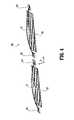
- FIG. 1schematically illustrates an antenna that comprises wires as radiating elements, which can be designed in accordance with specifications for a fine pitch wire bonding methods, according to an exemplary embodiment of the invention.
- FIG. 2Ais a schematic plan view of an antenna according to an exemplary embodiment of the invention.
- FIG. 2Bis a schematic cross-sectional side view of the exemplary antenna depicted in FIG. 2A taken along line 2 B- 2 B.
- FIG. 3is a schematic perspective view of an apparatus for integrally packaging an antenna and IC (integrated circuit) chip, according to an exemplary embodiment of the present invention.
- FIG. 4depicts a computer model of a dipole antenna according to an exemplary embodiment of the invention.
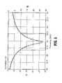
- FIG. 5graphically illustrates a simulated return loss of the model dipole antenna of FIG. 4 .
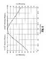
- FIG. 6graphically illustrates the simulated antenna and radiation efficiency of the model dipole antenna of FIG. 4 .
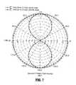
- FIG. 7graphically illustrates simulated radiation patterns of the model dipole antenna of FIG. 4 .
- FIGS. 8A ⁇ 8Dare schematic illustrations of various types of antennas that can be formed using wire bonds, according to exemplary embodiments of the invention.
- Exemplary embodiments of the invention as described hereininclude apparatus and methods for constructing antennas using one or more wire elements as radiating elements attached to the surface of a substrate or semiconductor chip.
- the wirescomprise wire bonds that are formed using wire bond methods to attach wires to a substrate or chip and form the desired wire loop profiles.
- Antenna devices according to exemplary embodiments of the invention which are formed with wire bond radiating elementsutilize wire loop profiles that are feasible and consistent with the limitations of current (or future) bonding technologies in terms of wire dimensions, precision and motion contours, for example.
- the use of wire bonding methods to form wires as radiating elementsenables accurate placement and repeatability for high volume manufacturing of antenna devices according to the invention. A brief description of wire bonding methods and the use of such methods for constructing antenna devices according to exemplary embodiments of the invention will now be provided.
- wire bondingis a method that is commonly used in semiconductor fabrication for making chip-to-substrate interconnections to provide electrical paths for power and signal distribution.
- wire bondinggenerally involves connecting pads on a die to a lead frame (or substrate) using very fine diameter wire.
- wire bonding methodsthat can be implemented, which are known as “ball bonding” and “wedge bonding” methods.
- the basic steps for both types of wire bonding methodsinclude (i) forming a first bond (normally on the chip), (ii) forming a wire loop, and (iii) forming a second bond (normally on the substrate).
- ball bondinga free air ball is formed at the beginning of each bond cycle and the first bond is achieved by bonding the ball to the pad
- wedge bondinga wire is bonded directly to a device using force and ultrasonic energy.
- bond wire formed of gold (Au) wire having a purity of at least 99.99%is typically used.
- copper (Cu) wirescan be ball bonded by making some modifications to a wire bond device. In such a case, a gas environment is formed to prevent Cu oxidation during the free air ball formation.
- Both Au and Cu bondingare performed at elevated temperatures, a process referred to as “thermosonic bonding” because it employs heat and ultrasonic energy.
- wire bondscould be formed using Au wire at elevated temperatures or using aluminum (Al) wire at room temperature.
- the loop of a wire bondrefers to the curve or arc of the wire between the attachment points at each end of a wire bond.
- ball bondingplaces no restrictions on the direction for looping a wire from the first bond to the second bond, which renders ball bonding looping extremely flexible.
- conventional wedge bonding equipmentonly allows bonds to be placed parallel to the wire direction.
- Another difference between ball bonding and wedge bondingis that the speed of bonding using ball bonding can be more than twice the speed of the fastest wedge bonder.
- ball bonding or wedge bonding methodscan be used for forming wire bonds as radiating elements on a substrate or chip. Due to the higher speed, lower cost, and more flexible looping capability, ball bonding is the most commonly used interconnect method today. However, for fine pitch applications, when selecting between ball bonding or wedge bonding, several factors including achieving small, reliable bonds, maintaining loops, and positioning the bond accurately, should be considered.
- FIG. 1schematically illustrates an antenna that comprises wires as radiating elements, which can be designed using fine pitch wire bonding methods in accordance with the specifications as listed in Table I, according to exemplary embodiments of the invention. More specifically, FIG. 1 schematically illustrates a dipole antenna ( 10 ) comprising a half-wavelength dipole element comprising first and second quarter-wave wire elements ( 11 ) and ( 12 ) which are connected to respective ball bonds ( 13 ) and ( 14 ). In FIG. 1 , it is assumed that the ball bonds are bonded to pad connections of a feed network (e.g., differential feed network) and the opposite ends of the wires ( 11 ) and ( 12 ) are connected to a substrate or chip (as explained below with reference to FIGS. 2A , 2 B and 3 , for example).
- a feed networke.g., differential feed network
- wire bonding tools for fine-pitch ball and wire bondingare capable of producing a bond pitch (B P ) (spacing between wire bonds on a chip, for example) of 35-45 microns (and a minimum 35 micron ball bond pitch (B P ) for ball bonding), a minimum wire diameter of 15-25.4 microns, a wire sway of ⁇ 1 wire diameter for high precision wire spans of less than 2.4 mm, a 3 ⁇ standard deviation) placement accuracy (PA) of ⁇ 5 microns, a maximum wire bond length (L W ) of 7.6 mm, a minimum wire loop height (LH) of 100 microns, and a minimum ball diameter (B D ) of 43 microns.
- these wire bond specificationsare suitable for constructing antenna devices with wire bonds as radiating elements for millimeter wave applications.
- wire bonding toolsallow several wire loops to be programmed, e.g. J-wire loop, RF loop, spinder loop profile, etc. Most of the available loop profiles are derived with experimental statistical methods applied to the possible motion contours of a wire bonding tool tip. Typically, known and commonly used shapes/contours/loop profiles are related to a specific package type or chip attachment technique to provide the shortest wire bond possible and/or smallest bonding pitch without necking the wire.
- Bonding wire profile limitationscan be analyzed by modeling a wire bond as a plurality of sets of corresponding linkage/spring pairs, which are combined to form a wire bond, wherein the coefficients of elasticity and plasticity of the springs are determined by the bending angle of two linkages, which simulates the elastic-plastic deformation of the bonding wires.
- These studiescan be used to illustrate that there are a variety of wire loop profiles, which are not desirable for chip-to-substrate interconnects, but which are suitable and effective as radiating elements for antennas in accordance with exemplary embodiments of the invention.
- Manual wire bonderscan be used to exploit the contour motions process to achieve wire loop profiles which comply with the capabilities of automated fine-pitch wire bonding tools.
- Exemplary embodiments of the invention as described hereinutilize wire loop profiles that are feasible and consistent with the limitations of a wire bonding technology in terms of wire dimensions, precision and motion contours.
- FIGS. 2A and 2Bare schematic diagrams illustrating an antenna device according to an exemplary embodiment of the present invention. More specifically, FIGS. 2A and 2B illustrate an exemplary embodiment antenna device ( 20 ) comprising a dipole antenna formed with wire bonds as radiating elements, wherein FIG. 2A schematically illustrates a top plan view of the antenna device ( 20 ) and FIG. 2B is a schematic cross-sectional view of the antenna device ( 20 ) of FIG. 2A taken along line 2 B- 2 B.
- exemplary embodiments of the inventionwill be described with specific reference to dipole antenna devices and integration of such devices in semiconductor IC packages. It is to be understood, however, that the present invention is not limited to any particular antenna type or operating frequency. Rather, the invention is more generally applicable to any antenna type that is suitable for a given application and/or frequency of operation, which can be designed using wires as radiating elements formed with wire bonding methods, for example.
- an exemplary antenna device ( 20 )comprises a substrate ( 21 ) (or chip (die)) having a dipole antenna structure based on the exemplary framework of FIG. 1 . More specifically, the dipole antenna comprises a first wire element ( 22 ) connected to and supported by metallic pads ( 23 ) and ( 24 ), and a second wire element ( 25 ) connected to and supported by metallic pads ( 26 ) and ( 27 ).
- the first and second wire elements ( 22 ) and ( 25 )are first and second quarter-wave wire elements, respectively.
- the metallic pads ( 23 ) and ( 26 )are contact pads to an integrated antenna feed network connected to an RF circuit.
- the metallic pads ( 24 ) and ( 27 )are termination pads for attaching and supporting the end (non-fed) portions of respective wire elements ( 22 ) and ( 25 ). Each wire has a starting and end point where it is connected and supported.
- the exemplary antenna device ( 20 )further comprises optional metallic shielding elements ( 28 ) and ( 29 ) formed on the substrate/chip ( 21 ) under respective wire elements ( 22 ) and ( 25 ).
- the metallic shielding elements ( 28 ) and ( 29 )may be included between the substrate ( 21 ) and the wires ( 22 ) and ( 25 ) to prevent electromagnetic fields from penetrating into the substrate ( 21 ) thereby reducing loss and improving the antenna efficiency.
- the contact pads ( 23 ), ( 24 ), ( 26 ) and ( 27 ) and shielding elements ( 28 ) and ( 29 )can be formed as part of the top metallization layer of the substrate/chip ( 21 ).
- the substrate/chip ( 21 )may comprise any suitable material including, for example, dielectric/insulative materials such as fused silica (SiO 2 ), alumina, polystyrene, ceramic, teflon based substrates, FR4, etc., or semiconductor materials such as high resistivity silicon or GaAs, etc.
- dielectric/insulative materialssuch as fused silica (SiO 2 ), alumina, polystyrene, ceramic, teflon based substrates, FR4, etc.
- semiconductor materialssuch as high resistivity silicon or GaAs, etc.
- the exemplary antenna device ( 20 )comprises an antenna encapsulation layer ( 30 ) for environmental protection, which is shown in FIGS. 2A and 2B in phantom (dotted lines).
- the encapsulation layer ( 30 )may be a package cover (plastic cover) that encapsulates the antenna and substrate/chip.
- the chip and antennacan be encapsulated in a low cost plastic package.
- a layer of dielectric materialmay be formed over the substrate/chip ( 21 ) such that the antenna wire elements are embedded within such layer.
- the wire elements ( 22 ) and ( 25 )are attached to the substrate/chip ( 21 ), and the loop profiles of such wire elements are formed, using a wire bonding machine, which enables accurate placement and repeatability for high volume manufacturing.
- loop profiles according to exemplary embodiments of the inventioncan be programmed to the wire bonder using known techniques to provide an optimum/desired radiation efficiency for a given antenna type.
- FIGS. 2A and 2Billustrate various parameters and/or dimensions for the exemplary dipole antenna device ( 20 ), which can be varied depending on the application, antenna type, and/or frequency of operation, for example.
- the substrate/chip ( 21 )is depicted as substantially square-shaped with area dimensions (C X ) and (C Y ) and with a thickness of (C Z ).
- the encapsulant/cover ( 30 )is depicted as having dimensions (P X ), (P Y ) and (P Z ).
- the wire elements ( 22 ) and ( 25 )are depicted as each having a wire diameter (D W ) , a lateral span (S), and feed points separated by pitch (P).
- the metallic contact pads ( 23 ), ( 24 ), ( 26 ), and ( 27 )are depicted as having a width (W C ) and the metallic shields ( 28 ) and ( 29 ) are depicted as having a width (W S ).
- the termination pads ( 24 ) and ( 27 )are depicted as being separated with a lateral extension (L) across the substrate/chip ( 21 ).
- the feed pads ( 23 ) and ( 26 )are depicted as being separated by a gap (G F ) and the metallic shields and contact pads are depicted as being separated with a gap (G).
- the wire elements ( 22 ) and ( 25 )are depicted as having a loop height (LH) over the respective metallic shields ( 28 ) and ( 29 ).
- Table IIlists exemplary values for the above parameters/dimensions for a 60 GHz dipole antenna design based on the framework of FIGS. 2A and 2B , according to an exemplary embodiment of the invention.
- the loop height (LH) of 100 ⁇ mis suitable for implementation with a chip and package having the listed dimensions.
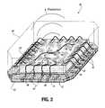
- FIG. 3is a schematic perspective view of an apparatus ( 40 ) for integrally packaging an antenna and IC chip, according to an exemplary embodiment of the present invention.
- FIG. 3illustrates a fully integrated on-chip dipole antenna having a framework similar to that discussed above with reference to the exemplary embodiments of FIGS. 2A and 2B , which is packaged with an IC chip using a low cost QFN (Quad Flat Nonleaded) package structure.
- QFNQuad Flat Nonleaded
- the apparatus ( 40 )comprises an IC chip ( 41 ) surface mounted to a leadless (ceramic) chip carrier ( 42 ), and a package encapsulation ( 43 ) (package cover) depicted in phantom (dotted lines) that encapsulates the IC package, which can be formed of a low-cost plastic material.
- the chip carrier ( 42 )comprises a lead frame having plurality of pads ( 44 ) formed on all four sides of the carrier substrate ( 42 ).
- the chip ( 41 ) (or die)comprises a plurality of bond pads ( 45 ) (or metallized regions) distributed around the perimeter of the active surface of the chip ( 41 ).
- the bond pads ( 45 )are connected to the lead frame pads ( 44 ) with wires ( 46 ) formed via wire bonding, for making electrical connections (e.g., ground, power, I/O, etc.) between the IC chip ( 41 ) and the package contacts ( 44 ).
- the chip carrier ( 42 )further comprises a die paddle ( 47 ) to which the die ( 41 ) is attached.
- the apparatus ( 40 )comprises a dipole antenna having a framework similar to the dipole antenna discussed above with reference to FIGS. 2A and 2B .
- the exemplary dipole antenna in FIG. 4comprises a first wire element ( 48 ) connected to and supported by metallic pads ( 49 ) and ( 50 ), and a second wire element ( 51 ) connected to and supported by metallic pads ( 52 ) and ( 53 ).
- the first and second wire elements ( 48 ) and ( 51 )are first and second quarter-wave wire elements, respectively.
- the metallic pads ( 49 ) and ( 52 )are contact pads to an integrated antenna feed network connected to an RF circuit.
- the metallic pads ( 50 ) and ( 53 )are termination pads for attaching and supporting end (non-fed) portions of respective wire elements ( 48 ) and ( 51 ).
- the contact pads ( 49 ) and ( 52 )enable connection of the dipole antenna to an integrated antenna feed network (differential feed), which is connected to an integrated circuit of the chip ( 41 ).
- the feed network frameworkwill vary depending on, e.g., the impedance that is desired for the given application and/or the type of devices to which the antenna will be connected. For example, if the antenna is connected to a transmitter system, the feed network will be designed to provide the proper connections and impedance matching for a power amplifier. By way of further example, if the antenna is connected to a receiver system, the feed network will be designed to provide the proper connections and impedance matching for a LNA (low noise amplifier).
- LNAlow noise amplifier
- the exemplary apparatus ( 40 )may further comprise metallic shielding elements formed on the chip ( 41 ) under wire elements ( 48 ) and ( 51 ) to prevent electromagnetic fields from penetrating into the substrate ( 41 ), depending on the substrate loss and its dielectric constant.
- the size of the ground shieldscan influence the radiation efficiency of the antenna and will be limited by the overall chip geometry.
- FIG. 3is merely one illustrative embodiment of a fully integrated on-chip antenna, and that one of ordinary skill in the art can readily envision other frameworks based on the teachings herein.
- antenna structures other than dipole antennascan be formed with wire bonds and packaged as described above.
- FIGS. 8A ⁇ 8D described belowschematically illustrate various antennas that can be built using wire bonds according to exemplary embodiments of the invention.
- IC packages according to other exemplary embodiments of the inventionmay be built with two antennas, wherein one antenna is connected to an integrated transmitter circuit for transmitting and another antenna is connected to an integrated receiver circuit for receiving, for example.
- FIG. 3is merely one illustrative embodiment of a fully integrated on-chip antenna, and that one of ordinary skill in the art can readily envision other frameworks based on the teachings herein.
- antenna structures other than dipole antennascan be formed with wire bonds and packaged as described above.
- FIGS. 8A ⁇ 8D described belowschematically illustrate various antennas that can be built using wire
- antennascan be formed with wire terminations located on a package lead ( 44 ) if larger wire spans are considered. Indeed, one or more lead wires can also be used as radiating elements of an antenna.
- simulationswere performed for 60 GHz dipole antenna design using the commercially available and well-known IE3D EM (electromagnetic) simulation software, which is an EM simulation software tool for RF, wireless, packaging, and optoelectronic design.
- simulationswere performed for a model differential-fed dipole antenna ( 60 ) in an air (vacuum) environment as depicted in FIG. 4 , with wire elements ( 61 ) and ( 62 ), contact pads ( 63 ), ( 64 ), ( 65 ) and ( 66 ) and metallic shields ( 67 ) and ( 68 ).
- model dipole antenna60
- Sloop span
- shields300 microns in width
- FIG. 5graphically illustrates a simulated return loss of the model dipole antenna ( 60 ) in air of FIG. 4 .
- FIG. 5graphically illustrates the simulated input impedance match parameters (S 11 ) in dB for the model 60 GHz dipole antenna.
- FIG. 5illustrates that the exemplary dipole antenna embodiment provides a bandwidth of about 6 GHz at the 60 GHz frequency band, wherein the bandwidth is defined based on the frequency range for which S 11 was measured to be about ⁇ 10 dB or better relative to a 75 Ohm feeding cable.
- FIG. 6graphically illustrates the simulated antenna and radiation efficiency of the model dipole antenna of FIG. 4 .
- a ground shieldmay be used to prevent the electromagnetic fields from reaching into the substrate and the size of such ground shields will influence the radiation efficiency.
- FIG. 7graphically illustrates (using a polar graph) the simulated elevation radiation patterns of the model 60 GHz dipole antenna of FIG. 4 .
- the elevation radiation patterns depicted in FIG. 7assume a Cartesian coordinate system as depicted in FIG. 4 , wherein the Z-axis extends in a direction perpendicular to the plane of the antenna shields and pads, wherein the x-axis longitudinally extends along the plane of the antenna in a direction along axis of the dipole antenna, and wherein the y-axis longitudinally extends in a direction perpendicular to the axis of the dipole antenna.
- the exemplary embodiments discussed above with reference to FIGS. 1 , 2 A, 2 B, and 3are merely exemplary embodiments of antennas and IC packages according to the invention, and that one of ordinary skill in the art can readily envision other antenna types that can be constructed and packaged with IC chips using the devices and methods of the present invention.
- other antennassuch as monopole, folded dipole, loop or end-fire antenna array structures, for example, can be constructed using wire elements according to the invention.
- intermediate connectionscan be provided to form a meander wire structure on-chip.
- FIGS. 8A ⁇ 8Dare schematic diagrams illustrating antennas that can be built using wire bonds, according to exemplary embodiments of the invention.
- the exemplary antenna frameworks depicted in FIGS. 8A ⁇ 8Dcan be packaged with IC chips as discussed above with reference to FIG. 3 , for example.
- FIG. 8Aschematically illustrates a loop antenna ( 70 ) that is formed with a plurality of separate wire bond elements ( 71 a ⁇ 71 e ) arranged in a loop, which are connected to corresponding pads ( 72 ⁇ 77 ).
- pads ( 72 ) and ( 77 )are assumed to be feed points (e.g., differential feed) to a feed network.
- pads ( 73 ⁇ 76 )are shown to be connection points for the various wire bond elements, which enable a meandering wire structure.
- FIG. 8Bschematically illustrates a folded dipole antenna ( 80 ), which is formed using three wire bonds ( 81 a , 81 b , 81 c ) and pads ( 82 ⁇ 85 ).
- the wire bond elements ( 81 a ) and ( 81 b )are quarter-wave elements that comprise a first (fed) half-wavelength dipole element
- the wire bond element ( 81 c )comprises a second half-wavelength dipole element.
- the first and second half-wavelength elementsare disposed substantial parallel to each other and separated by a gap.
- the end portions of elements ( 81 a ) and ( 81 b )are connected (shorted) to end portions of the second dipole element ( 81 c ) by contact pads ( 84 ) and ( 85 ).
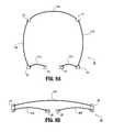
- FIG. 8Cschematically illustrates a monopole antenna ( 90 ) according to an exemplary embodiment of the invention.
- the monopole antenna ( 90 )is formed using one wire bond ( 91 ) attached to pads ( 92 ) and ( 93 ).
- FIG. 8Dschematically illustrates an end-fire antenna array ( 100 ) according to an exemplary embodiment of the invention.
- the exemplary antenna ( 100 )comprises a plurality of parallel half-wave elements ( 101 ⁇ 104 ) connected to respective pads ( 105 ⁇ 112 ).
- the elements ( 101 ⁇ 104 )can be feed with current that is 180 degrees out of phase.
- antenna devices according to exemplary embodiments of the inventioncan operate at RF and microwave frequencies, for example, while simultaneously providing antenna performance characteristics such as high gain/directivity/radiation efficiency, wide bandwidth, hemishperical or omnidirectional radiation patterns, impedance, etc., that render the antennas suitable for voice communication, data communication or radar applications, for example.
- exemplary antenna designs according to the inventionenable high-volume antenna manufacturing capability.
- integrated IC packages according to exemplary embodiments of the inventionenable antennas to be integrally packaged with IC chips such as transceiver chips, which provide compact designs with very low loss between the transceiver and the antenna. Indeed, such IC package designs eliminate the need to go off the transceiver chip with high frequency input and output signals, thereby providing low loss designs.
- antennas and integrated antenna packages according to the present inventionenable a multitude of applications such as integrated phased array antenna systems, personal area networks, radar feeds, high reliability due to redundancy, point-to-point systems, etc.
- the use of integrated antenna/IC chip packages according to the present inventionsaves significant space, size, cost and weight, which is a premium for virtually any commercial or military application.
- antennascan be constructed having an array of two or more antennas formed on a substrate to provide an antenna with desired directivity for beamforming or beamsteering antenna applications.
- a directive antenna beam patterncan be obtained using a phased array antenna, wherein the input signal phase to each wire bond antenna is controlled to electronically scan or steer the directive antenna pattern to a desired direction.
Landscapes
- Engineering & Computer Science (AREA)
- Microelectronics & Electronic Packaging (AREA)
- Computer Hardware Design (AREA)
- Power Engineering (AREA)
- Details Of Aerials (AREA)
- Variable-Direction Aerials And Aerial Arrays (AREA)
Abstract
Description
| TABLE I | |||
| PARAMETERS | TYPICAL VALUES | ||
| Bond Pitch (Bp) | 35-45 microns | ||
| Minimum Wire Diameter (WD) | 15-25.4 microns | ||
| Wire Sway | +/−1 Wire Diameter | ||
| Maximum Wire Bond Length (Lw) | 7.6 mm | ||
| High Precision Wire Spans | <2.4 mm | ||
| 3σ Placement Accuracy (PA) | +/−5 microns | ||
| Minimum Loop Height (LH) | 100 microns | ||
| Minimum Ball Diameter (BD) | 43 microns | ||
| TABLE II | |
| PARAMETER | EXEMPLARY VALUE |
| Chip/Substrate Dimension (CX) | 2.5 mm |
| Chip/Substrate Dimension (CY) | 2.5 mm |
| Chip/Substrate Dimension (CZ) | 300 microns |
| Wire Span (S) | 1012.5 microns |
| Wire Loop Height (LH) | 100 microns |
| Wire Pitch (P) | 175 microns |
| Wire Diameter (DW) | 25.4 microns |
| Wire Feed Gap (GF) | 50 microns |
| Lateral On-Chip Antenna Extension (L) | 2300 microns |
| Encapsulant Dimension (PX) | 5 mm |
| Encapsulant Dimension (PY) | 5 mm |
| Encapsulant Dimension (PZ) | 800 microns |
| Width of Contact Pads (WC) | 100 microns |
| Width of Shields (WS) | 300 microns |
| Gap between Contact Pads /Shields (G) | 50 microns |
Claims (28)
Priority Applications (8)
| Application Number | Priority Date | Filing Date | Title |
|---|---|---|---|
| US10/912,959US7295161B2 (en) | 2004-08-06 | 2004-08-06 | Apparatus and methods for constructing antennas using wire bonds as radiating elements |
| JP2007524785AJP4608547B2 (en) | 2004-08-06 | 2005-02-23 | Apparatus and method for constructing an antenna using wire bonds as radiating elements |
| CN200580023253.XACN101023560B (en) | 2004-08-06 | 2005-02-23 | Apparatus and method for constructing an antenna using bonded wires as radiating elements |
| CA2575845ACA2575845C (en) | 2004-08-06 | 2005-02-23 | Apparatus and methods for constructing antennas using wire bonds as radiating elements |
| KR1020077002561AKR100962848B1 (en) | 2004-08-06 | 2005-02-23 | Antenna Devices, Integrated Communications Devices, and IC Package Devices |
| PCT/US2005/005706WO2006022836A1 (en) | 2004-08-06 | 2005-02-23 | Apparatus and methods for constructing antennas using wire bonds as radiating elements |
| EP05723543AEP1782503A1 (en) | 2004-08-06 | 2005-02-23 | Apparatus and methods for constructing antennas using wire bonds as radiating elements |
| TW094126138ATWI356525B (en) | 2004-08-06 | 2005-08-02 | Apparatus and methods for constructing antennas us |
Applications Claiming Priority (1)
| Application Number | Priority Date | Filing Date | Title |
|---|---|---|---|
| US10/912,959US7295161B2 (en) | 2004-08-06 | 2004-08-06 | Apparatus and methods for constructing antennas using wire bonds as radiating elements |
Publications (2)
| Publication Number | Publication Date |
|---|---|
| US20060028378A1 US20060028378A1 (en) | 2006-02-09 |
| US7295161B2true US7295161B2 (en) | 2007-11-13 |
Family
ID=34961149
Family Applications (1)
| Application Number | Title | Priority Date | Filing Date |
|---|---|---|---|
| US10/912,959Expired - LifetimeUS7295161B2 (en) | 2004-08-06 | 2004-08-06 | Apparatus and methods for constructing antennas using wire bonds as radiating elements |
Country Status (8)
| Country | Link |
|---|---|
| US (1) | US7295161B2 (en) |
| EP (1) | EP1782503A1 (en) |
| JP (1) | JP4608547B2 (en) |
| KR (1) | KR100962848B1 (en) |
| CN (1) | CN101023560B (en) |
| CA (1) | CA2575845C (en) |
| TW (1) | TWI356525B (en) |
| WO (1) | WO2006022836A1 (en) |
Cited By (174)
| Publication number | Priority date | Publication date | Assignee | Title |
|---|---|---|---|---|
| US20060250308A1 (en)* | 2005-03-31 | 2006-11-09 | Georgia Tech Research Corporation | Module,filter, and antenna technology millimeter waves multi-gigabits wireless systems |
| US20070103380A1 (en)* | 2005-10-07 | 2007-05-10 | Nhew R&D Pty Ltd. | Mm-wave antenna using conventional ic packaging |
| US20080072423A1 (en)* | 2006-09-26 | 2008-03-27 | Advanced Microelectronic And Automation Technology Ltd. | Secure high frequency / ultra high frequency inlay, and method and apparatus for making the inlay |
| US20080205495A1 (en)* | 2007-02-26 | 2008-08-28 | Trott Gary R | RF Transceiver Adapted for Signal Isolators and Proximity Sensors |
| US20080231518A1 (en)* | 2006-12-27 | 2008-09-25 | Kabushiki Kaisha Toshiba | Antenna device and radio communication device |
| US20080291107A1 (en)* | 2007-05-25 | 2008-11-27 | Freescale Semiconductor, Inc. | Antenna structure for integrated circuit die using bond wire |
| US20080315992A1 (en)* | 2007-06-22 | 2008-12-25 | Forster Ian J | Foldable rfid device interposer and method |
| US20090009405A1 (en)* | 2006-06-21 | 2009-01-08 | Broadcom Corporation | Integrated circuit with power supply line antenna structure and methods for use therewith |
| US20090009408A1 (en)* | 2006-06-21 | 2009-01-08 | Broadcom Corporation | Integrated circuit with bonding wire antenna structure and methods for use therewith |
| US20090207090A1 (en)* | 2007-06-22 | 2009-08-20 | Vubiq Incorporated | Integrated antenna and chip package and method of manufacturing thereof |
| US20100026605A1 (en)* | 2008-05-23 | 2010-02-04 | University Of Maryland | F-inverted compact antenna for wireless sensor networks and manufacturing method |
| US20100311369A1 (en)* | 2009-06-09 | 2010-12-09 | Ahmadreza Rofougaran | Method and system for communicating via leaky wave antennas within a flip-chip bonded structure |
| US20120105304A1 (en)* | 2010-10-28 | 2012-05-03 | Sony Corporation | Antenna |
| US8179333B2 (en)* | 2009-05-08 | 2012-05-15 | Anokiwave, Inc. | Antennas using chip-package interconnections for millimeter-wave wireless communication |
| US20130300614A1 (en)* | 2011-01-14 | 2013-11-14 | Yuji Machida | High frequency module |
| US8608080B2 (en) | 2006-09-26 | 2013-12-17 | Feinics Amatech Teoranta | Inlays for security documents |
| US20140231528A1 (en)* | 2009-09-09 | 2014-08-21 | Murata Manufacturing Co., Ltd. | Antenna, method of manufacturing the antenna, and wireless ic device |
| US20140354494A1 (en)* | 2013-06-03 | 2014-12-04 | Daniel A. Katz | Wrist Worn Device with Inverted F Antenna |
| US20150130681A1 (en)* | 2013-11-08 | 2015-05-14 | Taiwan Semiconductor Manufacturing Company, Ltd. | 3d antenna for integrated circuits |
| US9088058B2 (en) | 2009-08-19 | 2015-07-21 | Vubiq Networks, Inc. | Waveguide interface with a launch transducer and a circular interface plate |
| US9160055B2 (en) | 2012-12-12 | 2015-10-13 | Kabushiki Kaisha Toshiba | Wireless device |
| US9178269B2 (en) | 2011-07-13 | 2015-11-03 | Kabushiki Kaisha Toshiba | Wireless apparatus |
| US9184492B2 (en) | 2010-09-24 | 2015-11-10 | Kabushiki Kaisha Toshiba | Radio device |
| US9245866B2 (en) | 2010-01-05 | 2016-01-26 | Kabushiki Kaisha Toshiba | Antenna device and wireless apparatus |
| US20160099220A1 (en)* | 2014-10-01 | 2016-04-07 | Analog Devices Global | High isolation wideband switch |
| US9543641B2 (en) | 2011-07-13 | 2017-01-10 | Kabushiki Kaisha Toshiba | Wireless apparatus |
| US9608740B2 (en) | 2015-07-15 | 2017-03-28 | At&T Intellectual Property I, L.P. | Method and apparatus for launching a wave mode that mitigates interference |
| US9615269B2 (en) | 2014-10-02 | 2017-04-04 | At&T Intellectual Property I, L.P. | Method and apparatus that provides fault tolerance in a communication network |
| US9628116B2 (en) | 2015-07-14 | 2017-04-18 | At&T Intellectual Property I, L.P. | Apparatus and methods for transmitting wireless signals |
| US9640850B2 (en) | 2015-06-25 | 2017-05-02 | At&T Intellectual Property I, L.P. | Methods and apparatus for inducing a non-fundamental wave mode on a transmission medium |
| US9667317B2 (en) | 2015-06-15 | 2017-05-30 | At&T Intellectual Property I, L.P. | Method and apparatus for providing security using network traffic adjustments |
| US9674711B2 (en) | 2013-11-06 | 2017-06-06 | At&T Intellectual Property I, L.P. | Surface-wave communications and methods thereof |
| US9685992B2 (en) | 2014-10-03 | 2017-06-20 | At&T Intellectual Property I, L.P. | Circuit panel network and methods thereof |
| US9692101B2 (en) | 2014-08-26 | 2017-06-27 | At&T Intellectual Property I, L.P. | Guided wave couplers for coupling electromagnetic waves between a waveguide surface and a surface of a wire |
| US9699785B2 (en) | 2012-12-05 | 2017-07-04 | At&T Intellectual Property I, L.P. | Backhaul link for distributed antenna system |
| US9705610B2 (en) | 2014-10-21 | 2017-07-11 | At&T Intellectual Property I, L.P. | Transmission device with impairment compensation and methods for use therewith |
| US9705561B2 (en) | 2015-04-24 | 2017-07-11 | At&T Intellectual Property I, L.P. | Directional coupling device and methods for use therewith |
| US9722318B2 (en) | 2015-07-14 | 2017-08-01 | At&T Intellectual Property I, L.P. | Method and apparatus for coupling an antenna to a device |
| US9729197B2 (en) | 2015-10-01 | 2017-08-08 | At&T Intellectual Property I, L.P. | Method and apparatus for communicating network management traffic over a network |
| US9735833B2 (en) | 2015-07-31 | 2017-08-15 | At&T Intellectual Property I, L.P. | Method and apparatus for communications management in a neighborhood network |
| US9742462B2 (en) | 2014-12-04 | 2017-08-22 | At&T Intellectual Property I, L.P. | Transmission medium and communication interfaces and methods for use therewith |
| US9742521B2 (en) | 2014-11-20 | 2017-08-22 | At&T Intellectual Property I, L.P. | Transmission device with mode division multiplexing and methods for use therewith |
| US9748626B2 (en) | 2015-05-14 | 2017-08-29 | At&T Intellectual Property I, L.P. | Plurality of cables having different cross-sectional shapes which are bundled together to form a transmission medium |
| US9749013B2 (en) | 2015-03-17 | 2017-08-29 | At&T Intellectual Property I, L.P. | Method and apparatus for reducing attenuation of electromagnetic waves guided by a transmission medium |
| US9749053B2 (en) | 2015-07-23 | 2017-08-29 | At&T Intellectual Property I, L.P. | Node device, repeater and methods for use therewith |
| US9762289B2 (en) | 2014-10-14 | 2017-09-12 | At&T Intellectual Property I, L.P. | Method and apparatus for transmitting or receiving signals in a transportation system |
| US9768833B2 (en) | 2014-09-15 | 2017-09-19 | At&T Intellectual Property I, L.P. | Method and apparatus for sensing a condition in a transmission medium of electromagnetic waves |
| US9769128B2 (en) | 2015-09-28 | 2017-09-19 | At&T Intellectual Property I, L.P. | Method and apparatus for encryption of communications over a network |
| US9769020B2 (en) | 2014-10-21 | 2017-09-19 | At&T Intellectual Property I, L.P. | Method and apparatus for responding to events affecting communications in a communication network |
| US9780834B2 (en) | 2014-10-21 | 2017-10-03 | At&T Intellectual Property I, L.P. | Method and apparatus for transmitting electromagnetic waves |
| US9787412B2 (en) | 2015-06-25 | 2017-10-10 | At&T Intellectual Property I, L.P. | Methods and apparatus for inducing a fundamental wave mode on a transmission medium |
| US9793955B2 (en) | 2015-04-24 | 2017-10-17 | At&T Intellectual Property I, Lp | Passive electrical coupling device and methods for use therewith |
| US9793951B2 (en) | 2015-07-15 | 2017-10-17 | At&T Intellectual Property I, L.P. | Method and apparatus for launching a wave mode that mitigates interference |
| US9793954B2 (en) | 2015-04-28 | 2017-10-17 | At&T Intellectual Property I, L.P. | Magnetic coupling device and methods for use therewith |
| US9800327B2 (en) | 2014-11-20 | 2017-10-24 | At&T Intellectual Property I, L.P. | Apparatus for controlling operations of a communication device and methods thereof |
| US9820146B2 (en) | 2015-06-12 | 2017-11-14 | At&T Intellectual Property I, L.P. | Method and apparatus for authentication and identity management of communicating devices |
| US9838078B2 (en) | 2015-07-31 | 2017-12-05 | At&T Intellectual Property I, L.P. | Method and apparatus for exchanging communication signals |
| US9838896B1 (en) | 2016-12-09 | 2017-12-05 | At&T Intellectual Property I, L.P. | Method and apparatus for assessing network coverage |
| US9847850B2 (en) | 2014-10-14 | 2017-12-19 | At&T Intellectual Property I, L.P. | Method and apparatus for adjusting a mode of communication in a communication network |
| US9847566B2 (en) | 2015-07-14 | 2017-12-19 | At&T Intellectual Property I, L.P. | Method and apparatus for adjusting a field of a signal to mitigate interference |
| US9853342B2 (en) | 2015-07-14 | 2017-12-26 | At&T Intellectual Property I, L.P. | Dielectric transmission medium connector and methods for use therewith |
| US9860075B1 (en) | 2016-08-26 | 2018-01-02 | At&T Intellectual Property I, L.P. | Method and communication node for broadband distribution |
| US9866309B2 (en) | 2015-06-03 | 2018-01-09 | At&T Intellectual Property I, Lp | Host node device and methods for use therewith |
| US9866276B2 (en) | 2014-10-10 | 2018-01-09 | At&T Intellectual Property I, L.P. | Method and apparatus for arranging communication sessions in a communication system |
| US9865911B2 (en) | 2015-06-25 | 2018-01-09 | At&T Intellectual Property I, L.P. | Waveguide system for slot radiating first electromagnetic waves that are combined into a non-fundamental wave mode second electromagnetic wave on a transmission medium |
| US9871283B2 (en) | 2015-07-23 | 2018-01-16 | At&T Intellectual Property I, Lp | Transmission medium having a dielectric core comprised of plural members connected by a ball and socket configuration |
| US9871558B2 (en) | 2014-10-21 | 2018-01-16 | At&T Intellectual Property I, L.P. | Guided-wave transmission device and methods for use therewith |
| US9871282B2 (en) | 2015-05-14 | 2018-01-16 | At&T Intellectual Property I, L.P. | At least one transmission medium having a dielectric surface that is covered at least in part by a second dielectric |
| US9876570B2 (en) | 2015-02-20 | 2018-01-23 | At&T Intellectual Property I, Lp | Guided-wave transmission device with non-fundamental mode propagation and methods for use therewith |
| US9876264B2 (en) | 2015-10-02 | 2018-01-23 | At&T Intellectual Property I, Lp | Communication system, guided wave switch and methods for use therewith |
| US9876605B1 (en) | 2016-10-21 | 2018-01-23 | At&T Intellectual Property I, L.P. | Launcher and coupling system to support desired guided wave mode |
| US9882257B2 (en) | 2015-07-14 | 2018-01-30 | At&T Intellectual Property I, L.P. | Method and apparatus for launching a wave mode that mitigates interference |
| US9887447B2 (en) | 2015-05-14 | 2018-02-06 | At&T Intellectual Property I, L.P. | Transmission medium having multiple cores and methods for use therewith |
| US9893795B1 (en) | 2016-12-07 | 2018-02-13 | At&T Intellectual Property I, Lp | Method and repeater for broadband distribution |
| US9906269B2 (en) | 2014-09-17 | 2018-02-27 | At&T Intellectual Property I, L.P. | Monitoring and mitigating conditions in a communication network |
| US9904535B2 (en) | 2015-09-14 | 2018-02-27 | At&T Intellectual Property I, L.P. | Method and apparatus for distributing software |
| US9912382B2 (en) | 2015-06-03 | 2018-03-06 | At&T Intellectual Property I, Lp | Network termination and methods for use therewith |
| US9913139B2 (en) | 2015-06-09 | 2018-03-06 | At&T Intellectual Property I, L.P. | Signal fingerprinting for authentication of communicating devices |
| US9912419B1 (en) | 2016-08-24 | 2018-03-06 | At&T Intellectual Property I, L.P. | Method and apparatus for managing a fault in a distributed antenna system |
| US9911020B1 (en) | 2016-12-08 | 2018-03-06 | At&T Intellectual Property I, L.P. | Method and apparatus for tracking via a radio frequency identification device |
| US9912027B2 (en) | 2015-07-23 | 2018-03-06 | At&T Intellectual Property I, L.P. | Method and apparatus for exchanging communication signals |
| US9912033B2 (en) | 2014-10-21 | 2018-03-06 | At&T Intellectual Property I, Lp | Guided wave coupler, coupling module and methods for use therewith |
| US9917341B2 (en) | 2015-05-27 | 2018-03-13 | At&T Intellectual Property I, L.P. | Apparatus and method for launching electromagnetic waves and for modifying radial dimensions of the propagating electromagnetic waves |
| US9930668B2 (en) | 2013-05-31 | 2018-03-27 | At&T Intellectual Property I, L.P. | Remote distributed antenna system |
| US9927517B1 (en) | 2016-12-06 | 2018-03-27 | At&T Intellectual Property I, L.P. | Apparatus and methods for sensing rainfall |
| US9948354B2 (en) | 2015-04-28 | 2018-04-17 | At&T Intellectual Property I, L.P. | Magnetic coupling device with reflective plate and methods for use therewith |
| US9948333B2 (en) | 2015-07-23 | 2018-04-17 | At&T Intellectual Property I, L.P. | Method and apparatus for wireless communications to mitigate interference |
| US9948355B2 (en) | 2014-10-21 | 2018-04-17 | At&T Intellectual Property I, L.P. | Apparatus for providing communication services and methods thereof |
| US9954286B2 (en) | 2014-10-21 | 2018-04-24 | At&T Intellectual Property I, L.P. | Guided-wave transmission device with non-fundamental mode propagation and methods for use therewith |
| US9954287B2 (en) | 2014-11-20 | 2018-04-24 | At&T Intellectual Property I, L.P. | Apparatus for converting wireless signals and electromagnetic waves and methods thereof |
| US9967173B2 (en) | 2015-07-31 | 2018-05-08 | At&T Intellectual Property I, L.P. | Method and apparatus for authentication and identity management of communicating devices |
| US9973940B1 (en) | 2017-02-27 | 2018-05-15 | At&T Intellectual Property I, L.P. | Apparatus and methods for dynamic impedance matching of a guided wave launcher |
| US9991580B2 (en) | 2016-10-21 | 2018-06-05 | At&T Intellectual Property I, L.P. | Launcher and coupling system for guided wave mode cancellation |
| US9999038B2 (en) | 2013-05-31 | 2018-06-12 | At&T Intellectual Property I, L.P. | Remote distributed antenna system |
| US9998870B1 (en) | 2016-12-08 | 2018-06-12 | At&T Intellectual Property I, L.P. | Method and apparatus for proximity sensing |
| US9997819B2 (en) | 2015-06-09 | 2018-06-12 | At&T Intellectual Property I, L.P. | Transmission medium and method for facilitating propagation of electromagnetic waves via a core |
| US10009065B2 (en) | 2012-12-05 | 2018-06-26 | At&T Intellectual Property I, L.P. | Backhaul link for distributed antenna system |
| US10009067B2 (en) | 2014-12-04 | 2018-06-26 | At&T Intellectual Property I, L.P. | Method and apparatus for configuring a communication interface |
| US10009063B2 (en) | 2015-09-16 | 2018-06-26 | At&T Intellectual Property I, L.P. | Method and apparatus for use with a radio distributed antenna system having an out-of-band reference signal |
| US10020844B2 (en) | 2016-12-06 | 2018-07-10 | T&T Intellectual Property I, L.P. | Method and apparatus for broadcast communication via guided waves |
| US10027398B2 (en) | 2015-06-11 | 2018-07-17 | At&T Intellectual Property I, Lp | Repeater and methods for use therewith |
| US10027397B2 (en) | 2016-12-07 | 2018-07-17 | At&T Intellectual Property I, L.P. | Distributed antenna system and methods for use therewith |
| US10033108B2 (en) | 2015-07-14 | 2018-07-24 | At&T Intellectual Property I, L.P. | Apparatus and methods for generating an electromagnetic wave having a wave mode that mitigates interference |
| US10033107B2 (en) | 2015-07-14 | 2018-07-24 | At&T Intellectual Property I, L.P. | Method and apparatus for coupling an antenna to a device |
| US10044409B2 (en) | 2015-07-14 | 2018-08-07 | At&T Intellectual Property I, L.P. | Transmission medium and methods for use therewith |
| US10069535B2 (en) | 2016-12-08 | 2018-09-04 | At&T Intellectual Property I, L.P. | Apparatus and methods for launching electromagnetic waves having a certain electric field structure |
| US10079661B2 (en) | 2015-09-16 | 2018-09-18 | At&T Intellectual Property I, L.P. | Method and apparatus for use with a radio distributed antenna system having a clock reference |
| US10090606B2 (en) | 2015-07-15 | 2018-10-02 | At&T Intellectual Property I, L.P. | Antenna system with dielectric array and methods for use therewith |
| US10090594B2 (en) | 2016-11-23 | 2018-10-02 | At&T Intellectual Property I, L.P. | Antenna system having structural configurations for assembly |
| US10103801B2 (en) | 2015-06-03 | 2018-10-16 | At&T Intellectual Property I, L.P. | Host node device and methods for use therewith |
| US10103422B2 (en) | 2016-12-08 | 2018-10-16 | At&T Intellectual Property I, L.P. | Method and apparatus for mounting network devices |
| US10135146B2 (en) | 2016-10-18 | 2018-11-20 | At&T Intellectual Property I, L.P. | Apparatus and methods for launching guided waves via circuits |
| US10135147B2 (en) | 2016-10-18 | 2018-11-20 | At&T Intellectual Property I, L.P. | Apparatus and methods for launching guided waves via an antenna |
| US10135145B2 (en) | 2016-12-06 | 2018-11-20 | At&T Intellectual Property I, L.P. | Apparatus and methods for generating an electromagnetic wave along a transmission medium |
| US10136434B2 (en) | 2015-09-16 | 2018-11-20 | At&T Intellectual Property I, L.P. | Method and apparatus for use with a radio distributed antenna system having an ultra-wideband control channel |
| US10142086B2 (en) | 2015-06-11 | 2018-11-27 | At&T Intellectual Property I, L.P. | Repeater and methods for use therewith |
| US10139820B2 (en) | 2016-12-07 | 2018-11-27 | At&T Intellectual Property I, L.P. | Method and apparatus for deploying equipment of a communication system |
| US10144036B2 (en) | 2015-01-30 | 2018-12-04 | At&T Intellectual Property I, L.P. | Method and apparatus for mitigating interference affecting a propagation of electromagnetic waves guided by a transmission medium |
| US10148016B2 (en) | 2015-07-14 | 2018-12-04 | At&T Intellectual Property I, L.P. | Apparatus and methods for communicating utilizing an antenna array |
| US10170840B2 (en) | 2015-07-14 | 2019-01-01 | At&T Intellectual Property I, L.P. | Apparatus and methods for sending or receiving electromagnetic signals |
| US10168695B2 (en) | 2016-12-07 | 2019-01-01 | At&T Intellectual Property I, L.P. | Method and apparatus for controlling an unmanned aircraft |
| US10178445B2 (en) | 2016-11-23 | 2019-01-08 | At&T Intellectual Property I, L.P. | Methods, devices, and systems for load balancing between a plurality of waveguides |
| US10205655B2 (en) | 2015-07-14 | 2019-02-12 | At&T Intellectual Property I, L.P. | Apparatus and methods for communicating utilizing an antenna array and multiple communication paths |
| US10224634B2 (en) | 2016-11-03 | 2019-03-05 | At&T Intellectual Property I, L.P. | Methods and apparatus for adjusting an operational characteristic of an antenna |
| US10225025B2 (en) | 2016-11-03 | 2019-03-05 | At&T Intellectual Property I, L.P. | Method and apparatus for detecting a fault in a communication system |
| US10243784B2 (en) | 2014-11-20 | 2019-03-26 | At&T Intellectual Property I, L.P. | System for generating topology information and methods thereof |
| US10243270B2 (en) | 2016-12-07 | 2019-03-26 | At&T Intellectual Property I, L.P. | Beam adaptive multi-feed dielectric antenna system and methods for use therewith |
| US10264586B2 (en) | 2016-12-09 | 2019-04-16 | At&T Mobility Ii Llc | Cloud-based packet controller and methods for use therewith |
| US10291311B2 (en) | 2016-09-09 | 2019-05-14 | At&T Intellectual Property I, L.P. | Method and apparatus for mitigating a fault in a distributed antenna system |
| US10291334B2 (en) | 2016-11-03 | 2019-05-14 | At&T Intellectual Property I, L.P. | System for detecting a fault in a communication system |
| US10298293B2 (en) | 2017-03-13 | 2019-05-21 | At&T Intellectual Property I, L.P. | Apparatus of communication utilizing wireless network devices |
| US10305190B2 (en) | 2016-12-01 | 2019-05-28 | At&T Intellectual Property I, L.P. | Reflecting dielectric antenna system and methods for use therewith |
| US10312567B2 (en) | 2016-10-26 | 2019-06-04 | At&T Intellectual Property I, L.P. | Launcher with planar strip antenna and methods for use therewith |
| US10320586B2 (en) | 2015-07-14 | 2019-06-11 | At&T Intellectual Property I, L.P. | Apparatus and methods for generating non-interfering electromagnetic waves on an insulated transmission medium |
| US10320047B2 (en) | 2009-08-19 | 2019-06-11 | Vubiq Networks, Inc. | Waveguide assembly comprising a molded waveguide interface having a support block for a launch transducer that is coupled to a communication device through a flange attached to the interface |
| US10326494B2 (en) | 2016-12-06 | 2019-06-18 | At&T Intellectual Property I, L.P. | Apparatus for measurement de-embedding and methods for use therewith |
| US10326689B2 (en) | 2016-12-08 | 2019-06-18 | At&T Intellectual Property I, L.P. | Method and system for providing alternative communication paths |
| US10340983B2 (en) | 2016-12-09 | 2019-07-02 | At&T Intellectual Property I, L.P. | Method and apparatus for surveying remote sites via guided wave communications |
| US10340601B2 (en) | 2016-11-23 | 2019-07-02 | At&T Intellectual Property I, L.P. | Multi-antenna system and methods for use therewith |
| US10340600B2 (en) | 2016-10-18 | 2019-07-02 | At&T Intellectual Property I, L.P. | Apparatus and methods for launching guided waves via plural waveguide systems |
| US10340603B2 (en) | 2016-11-23 | 2019-07-02 | At&T Intellectual Property I, L.P. | Antenna system having shielded structural configurations for assembly |
| US10341142B2 (en) | 2015-07-14 | 2019-07-02 | At&T Intellectual Property I, L.P. | Apparatus and methods for generating non-interfering electromagnetic waves on an uninsulated conductor |
| US10340573B2 (en) | 2016-10-26 | 2019-07-02 | At&T Intellectual Property I, L.P. | Launcher with cylindrical coupling device and methods for use therewith |
| US10355367B2 (en) | 2015-10-16 | 2019-07-16 | At&T Intellectual Property I, L.P. | Antenna structure for exchanging wireless signals |
| US10359749B2 (en) | 2016-12-07 | 2019-07-23 | At&T Intellectual Property I, L.P. | Method and apparatus for utilities management via guided wave communication |
| US10361489B2 (en) | 2016-12-01 | 2019-07-23 | At&T Intellectual Property I, L.P. | Dielectric dish antenna system and methods for use therewith |
| US10374316B2 (en) | 2016-10-21 | 2019-08-06 | At&T Intellectual Property I, L.P. | System and dielectric antenna with non-uniform dielectric |
| US10382976B2 (en) | 2016-12-06 | 2019-08-13 | At&T Intellectual Property I, L.P. | Method and apparatus for managing wireless communications based on communication paths and network device positions |
| US10389037B2 (en) | 2016-12-08 | 2019-08-20 | At&T Intellectual Property I, L.P. | Apparatus and methods for selecting sections of an antenna array and use therewith |
| US10389029B2 (en) | 2016-12-07 | 2019-08-20 | At&T Intellectual Property I, L.P. | Multi-feed dielectric antenna system with core selection and methods for use therewith |
| US10411356B2 (en) | 2016-12-08 | 2019-09-10 | At&T Intellectual Property I, L.P. | Apparatus and methods for selectively targeting communication devices with an antenna array |
| US10439675B2 (en) | 2016-12-06 | 2019-10-08 | At&T Intellectual Property I, L.P. | Method and apparatus for repeating guided wave communication signals |
| US10446936B2 (en) | 2016-12-07 | 2019-10-15 | At&T Intellectual Property I, L.P. | Multi-feed dielectric antenna system and methods for use therewith |
| US10490524B2 (en) | 2017-01-05 | 2019-11-26 | Fraunhofer-Gesellschaft Zur Foerderung Der Angewandten Forschung E.V. | Antenna apparatus having bond wires |
| US10498044B2 (en) | 2016-11-03 | 2019-12-03 | At&T Intellectual Property I, L.P. | Apparatus for configuring a surface of an antenna |
| US10530505B2 (en) | 2016-12-08 | 2020-01-07 | At&T Intellectual Property I, L.P. | Apparatus and methods for launching electromagnetic waves along a transmission medium |
| US10535928B2 (en) | 2016-11-23 | 2020-01-14 | At&T Intellectual Property I, L.P. | Antenna system and methods for use therewith |
| US10547348B2 (en) | 2016-12-07 | 2020-01-28 | At&T Intellectual Property I, L.P. | Method and apparatus for switching transmission mediums in a communication system |
| US10566679B2 (en) | 2017-01-05 | 2020-02-18 | Fraunhofer-Gesellschaft Zur Foerderung Der Angewandten Forschung E.V. | Ribbon bond antennas |
| US10601494B2 (en) | 2016-12-08 | 2020-03-24 | At&T Intellectual Property I, L.P. | Dual-band communication device and method for use therewith |
| US10637149B2 (en) | 2016-12-06 | 2020-04-28 | At&T Intellectual Property I, L.P. | Injection molded dielectric antenna and methods for use therewith |
| US10650940B2 (en) | 2015-05-15 | 2020-05-12 | At&T Intellectual Property I, L.P. | Transmission medium having a conductive material and methods for use therewith |
| US10665942B2 (en) | 2015-10-16 | 2020-05-26 | At&T Intellectual Property I, L.P. | Method and apparatus for adjusting wireless communications |
| US10694379B2 (en) | 2016-12-06 | 2020-06-23 | At&T Intellectual Property I, L.P. | Waveguide system with device-based authentication and methods for use therewith |
| US10727599B2 (en) | 2016-12-06 | 2020-07-28 | At&T Intellectual Property I, L.P. | Launcher with slot antenna and methods for use therewith |
| US10755542B2 (en) | 2016-12-06 | 2020-08-25 | At&T Intellectual Property I, L.P. | Method and apparatus for surveillance via guided wave communication |
| US10777873B2 (en) | 2016-12-08 | 2020-09-15 | At&T Intellectual Property I, L.P. | Method and apparatus for mounting network devices |
| US10797781B2 (en) | 2015-06-03 | 2020-10-06 | At&T Intellectual Property I, L.P. | Client node device and methods for use therewith |
| US10811767B2 (en) | 2016-10-21 | 2020-10-20 | At&T Intellectual Property I, L.P. | System and dielectric antenna with convex dielectric radome |
| US10818997B2 (en) | 2017-12-29 | 2020-10-27 | Vubiq Networks, Inc. | Waveguide interface and printed circuit board launch transducer assembly and methods of use thereof |
| US10819035B2 (en) | 2016-12-06 | 2020-10-27 | At&T Intellectual Property I, L.P. | Launcher with helical antenna and methods for use therewith |
| US10916969B2 (en) | 2016-12-08 | 2021-02-09 | At&T Intellectual Property I, L.P. | Method and apparatus for providing power using an inductive coupling |
| US10938108B2 (en) | 2016-12-08 | 2021-03-02 | At&T Intellectual Property I, L.P. | Frequency selective multi-feed dielectric antenna system and methods for use therewith |
| US11032819B2 (en) | 2016-09-15 | 2021-06-08 | At&T Intellectual Property I, L.P. | Method and apparatus for use with a radio distributed antenna system having a control channel reference signal |
Families Citing this family (39)
| Publication number | Priority date | Publication date | Assignee | Title |
|---|---|---|---|---|
| US7912499B2 (en)* | 2005-03-31 | 2011-03-22 | Black Sand Technologies, Inc. | Techniques for partitioning radios in wireless communication systems |
| US8467827B2 (en)* | 2005-03-31 | 2013-06-18 | Black Sand Technologies, Inc. | Techniques for partitioning radios in wireless communication systems |
| US20060276157A1 (en)* | 2005-06-03 | 2006-12-07 | Chen Zhi N | Apparatus and methods for packaging antennas with integrated circuit chips for millimeter wave applications |
| US7342299B2 (en)* | 2005-09-21 | 2008-03-11 | International Business Machines Corporation | Apparatus and methods for packaging antennas with integrated circuit chips for millimeter wave applications |
| US20090021352A1 (en)* | 2007-07-18 | 2009-01-22 | Murata Manufacturing Co., Ltd. | Radio frequency ic device and electronic apparatus |
| US7741720B2 (en)* | 2007-09-25 | 2010-06-22 | Silverbrook Research Pty Ltd | Electronic device with wire bonds adhered between integrated circuits dies and printed circuit boards |
| KR100946545B1 (en)* | 2007-11-29 | 2010-03-11 | 엘지이노텍 주식회사 | High frequency module |
| KR101014778B1 (en)* | 2008-02-28 | 2011-02-14 | 연세대학교 산학협력단 | Chip antenna and semiconductor package, and ultra-wideband communication system including the same |
| KR100973043B1 (en)* | 2008-02-29 | 2010-07-29 | 연세대학교 산학협력단 | Beamforming chip antennas and semiconductor packages, and short-range personal communication network systems including the same |
| CN102308435B (en)* | 2009-02-25 | 2014-07-30 | 京瓷株式会社 | High-frequency module |
| CA2765063C (en)* | 2009-06-10 | 2016-08-23 | The Regents Of University Of California | Milli-meter-wave-wireless-interconnect (m2w2 - interconnect) method for short-range communications with ultra-high data rate capability |
| KR101133146B1 (en)* | 2009-08-26 | 2012-04-06 | 연세대학교 산학협력단 | Bonding Wire Antenna Communication Module |
| WO2011025241A2 (en)* | 2009-08-26 | 2011-03-03 | 연세대학교 산학협력단 | Bonding wire antenna communication module |
| CN103119714B (en)* | 2010-09-21 | 2016-08-17 | 德克萨斯仪器股份有限公司 | Chip-to-chip communication using submillimeter waves and dielectric waveguides |
| US9252107B2 (en) | 2012-05-31 | 2016-02-02 | Skyworks Solutions, Inc. | Semiconductor package having a metal paint layer |
| US9286564B2 (en)* | 2012-11-20 | 2016-03-15 | Xerox Corporation | Apparatuses and methods for printed radio frequency identification (RFID) tags |
| JP2014110555A (en) | 2012-12-03 | 2014-06-12 | Samsung Electronics Co Ltd | Antenna device |
| US9362613B2 (en)* | 2013-03-07 | 2016-06-07 | Taiwan Semiconductor Manufacturing Company, Ltd. | Bond wire antenna |
| TWI518816B (en) | 2013-07-04 | 2016-01-21 | 先進科技新加坡有限公司 | Method and apparatus for measuring a free air ball size during wire bonding |
| CN104952820A (en)* | 2015-06-10 | 2015-09-30 | 苏州波锐捷通信技术有限公司 | Chip package using bonding wires for millimeter-wave radio frequency communication |
| CN105552063A (en)* | 2016-02-03 | 2016-05-04 | 深圳佰维存储科技有限公司 | System in a package (SIP) structure |
| TWI589059B (en)* | 2016-03-28 | 2017-06-21 | 矽品精密工業股份有限公司 | Electronic package |
| CN110022748A (en) | 2016-09-13 | 2019-07-16 | 基文影像公司 | Compact helical antenna for vivo devices |
| DE102017200129A1 (en) | 2017-01-05 | 2018-07-05 | Fraunhofer-Gesellschaft zur Förderung der angewandten Forschung e.V. | Ndip antenna |
| DE102017200131A1 (en) | 2017-01-05 | 2018-07-05 | Fraunhofer-Gesellschaft zur Förderung der angewandten Forschung e.V. | Antenna device, antenna array, electrical circuit with an antenna device and ribbon antenna |
| CN106602271B (en)* | 2017-02-20 | 2024-02-02 | 长城信息股份有限公司 | Structure-enhanced antenna |
| KR102209123B1 (en) | 2017-12-19 | 2021-01-28 | 삼성전자 주식회사 | A module including an antenna and a radio frequency device and base station including the module |
| WO2019147870A1 (en)* | 2018-01-24 | 2019-08-01 | Snap Inc. | Hybrid antenna system for wearable devices |
| CN108963420A (en)* | 2018-04-23 | 2018-12-07 | 易力声科技(深圳)有限公司 | A kind of high resiliency antenna being made by closing line |
| CN108538823B (en)* | 2018-04-25 | 2020-06-19 | 成都聚利中宇科技有限公司 | Packaging chip of integrated monopole antenna and processing method thereof |
| CN108987914A (en)* | 2018-07-05 | 2018-12-11 | 易力声科技(深圳)有限公司 | A kind of paster antenna for making frequency modulation using closing line |
| US11460525B2 (en)* | 2020-02-12 | 2022-10-04 | GE Precision Healthcare LLC | Systems and methods for toroidal twinax cable trap |
| US11276655B2 (en) | 2020-05-22 | 2022-03-15 | InnogritTechnologies Co., Ltd. | Ground reference shape for high speed interconnect |
| US11901623B2 (en)* | 2020-08-18 | 2024-02-13 | Georgia Tech Research Corporation | RF systems on antenna and method of fabrication |
| EP3979408A1 (en)* | 2020-09-30 | 2022-04-06 | Infineon Technologies Austria AG | Transmitter component, receiver component, transceiver circuit, and gate driver circuit with integrated antenna structure |
| ES3034294T3 (en) | 2021-01-11 | 2025-08-14 | Nexite Ltd | Contactless and automatic operations of a retail store |
| IT202100001301A1 (en)* | 2021-01-25 | 2022-07-25 | St Microelectronics Srl | SEMICONDUCTOR DEVICE AND CORRESPONDING MANUFACTURING PROCEDURE |
| CN119013673A (en) | 2021-12-13 | 2024-11-22 | 奈克赛特公司 | System, method and apparatus for contactless automatic operation of retail stores |
| CN115295509B (en)* | 2022-08-17 | 2025-05-30 | 甬矽电子(宁波)股份有限公司 | IC radio frequency packaging structure and method for preparing the same |
Citations (14)
| Publication number | Priority date | Publication date | Assignee | Title |
|---|---|---|---|---|
| US3940046A (en) | 1974-03-20 | 1976-02-24 | Libbey-Owens-Ford Company | Soldering apparatus |
| WO1996013793A1 (en) | 1994-10-27 | 1996-05-09 | International Business Machines Corporation | Method of making radio frequency identification tags |
| US5682143A (en) | 1994-09-09 | 1997-10-28 | International Business Machines Corporation | Radio frequency identification tag |
| JPH11306306A (en) | 1998-04-20 | 1999-11-05 | Sumitomo Electric Ind Ltd | Non-contact IC card |
| EP0977145A2 (en) | 1998-07-28 | 2000-02-02 | Kabushiki Kaisha Toshiba | Radio IC card |
| EP1069645A2 (en) | 1999-07-13 | 2001-01-17 | Shinko Electric Industries Co. Ltd. | Semiconductor device with an antenna and fabrication method therefor |
| US6373447B1 (en)* | 1998-12-28 | 2002-04-16 | Kawasaki Steel Corporation | On-chip antenna, and systems utilizing same |
| JP2002141722A (en)* | 2000-10-31 | 2002-05-17 | Toppan Forms Co Ltd | IC chip bridge type antenna |
| US20040245651A1 (en)* | 2003-06-09 | 2004-12-09 | Matsushita Electric Industrial Co., Ltd. | Semiconductor device and method for fabricating the same |
| US6885354B2 (en)* | 2002-10-28 | 2005-04-26 | Seiko Epson Corporation | Non-contact communication medium |
| US6900767B2 (en)* | 2001-09-28 | 2005-05-31 | Konica Corporation | IC card |
| US6910636B2 (en)* | 2002-06-11 | 2005-06-28 | Samsung Techwin Co., Ltd. | IC card and manufacturing method thereof |
| US20050139981A1 (en)* | 2003-12-24 | 2005-06-30 | Fujitsu Limited | High-frequency device |
| US6967282B2 (en)* | 2004-03-05 | 2005-11-22 | Raytheon Company | Flip chip MMIC on board performance using periodic electromagnetic bandgap structures |
Family Cites Families (5)
| Publication number | Priority date | Publication date | Assignee | Title |
|---|---|---|---|---|
| US5202752A (en)* | 1990-05-16 | 1993-04-13 | Nec Corporation | Monolithic integrated circuit device |
| US6281794B1 (en)* | 1998-01-02 | 2001-08-28 | Intermec Ip Corp. | Radio frequency transponder with improved read distance |
| JP5214082B2 (en)* | 2001-07-25 | 2013-06-19 | インヴェンサス・コーポレイション | Semiconductor device |
| EP1563570A1 (en)* | 2002-11-07 | 2005-08-17 | Fractus, S.A. | Integrated circuit package including miniature antenna |
| JP4379875B2 (en)* | 2004-08-30 | 2009-12-09 | 小林クリエイト株式会社 | RFID data carrier |
- 2004
- 2004-08-06USUS10/912,959patent/US7295161B2/ennot_activeExpired - Lifetime
- 2005
- 2005-02-23JPJP2007524785Apatent/JP4608547B2/ennot_activeExpired - Fee Related
- 2005-02-23CNCN200580023253.XApatent/CN101023560B/ennot_activeExpired - Lifetime
- 2005-02-23CACA2575845Apatent/CA2575845C/ennot_activeExpired - Fee Related
- 2005-02-23EPEP05723543Apatent/EP1782503A1/ennot_activeCeased
- 2005-02-23KRKR1020077002561Apatent/KR100962848B1/ennot_activeExpired - Fee Related
- 2005-02-23WOPCT/US2005/005706patent/WO2006022836A1/enactiveSearch and Examination
- 2005-08-02TWTW094126138Apatent/TWI356525B/ennot_activeIP Right Cessation
Patent Citations (15)
| Publication number | Priority date | Publication date | Assignee | Title |
|---|---|---|---|---|
| US3940046A (en) | 1974-03-20 | 1976-02-24 | Libbey-Owens-Ford Company | Soldering apparatus |
| US5682143A (en) | 1994-09-09 | 1997-10-28 | International Business Machines Corporation | Radio frequency identification tag |
| US5972156A (en)* | 1994-09-09 | 1999-10-26 | Intermec Ip Corp. | Method of making a radio frequency identification tag |
| WO1996013793A1 (en) | 1994-10-27 | 1996-05-09 | International Business Machines Corporation | Method of making radio frequency identification tags |
| JPH11306306A (en) | 1998-04-20 | 1999-11-05 | Sumitomo Electric Ind Ltd | Non-contact IC card |
| EP0977145A2 (en) | 1998-07-28 | 2000-02-02 | Kabushiki Kaisha Toshiba | Radio IC card |
| US6373447B1 (en)* | 1998-12-28 | 2002-04-16 | Kawasaki Steel Corporation | On-chip antenna, and systems utilizing same |
| EP1069645A2 (en) | 1999-07-13 | 2001-01-17 | Shinko Electric Industries Co. Ltd. | Semiconductor device with an antenna and fabrication method therefor |
| JP2002141722A (en)* | 2000-10-31 | 2002-05-17 | Toppan Forms Co Ltd | IC chip bridge type antenna |
| US6900767B2 (en)* | 2001-09-28 | 2005-05-31 | Konica Corporation | IC card |
| US6910636B2 (en)* | 2002-06-11 | 2005-06-28 | Samsung Techwin Co., Ltd. | IC card and manufacturing method thereof |
| US6885354B2 (en)* | 2002-10-28 | 2005-04-26 | Seiko Epson Corporation | Non-contact communication medium |
| US20040245651A1 (en)* | 2003-06-09 | 2004-12-09 | Matsushita Electric Industrial Co., Ltd. | Semiconductor device and method for fabricating the same |
| US20050139981A1 (en)* | 2003-12-24 | 2005-06-30 | Fujitsu Limited | High-frequency device |
| US6967282B2 (en)* | 2004-03-05 | 2005-11-22 | Raytheon Company | Flip chip MMIC on board performance using periodic electromagnetic bandgap structures |
Non-Patent Citations (2)
| Title |
|---|
| International Search Report, no dated provided! |
| Patent Abstract of Japan for publication No. 11306306, no dated provided! |
Cited By (223)
| Publication number | Priority date | Publication date | Assignee | Title |
|---|---|---|---|---|
| US8286328B2 (en) | 2005-03-31 | 2012-10-16 | Georgia Tech Research Corporation | Method of fabricating a module, for millimeter wave multi-gigabit wireless systems |
| US20110120628A1 (en)* | 2005-03-31 | 2011-05-26 | Georgia Tech Research Corporation | Module, Filter, And Antenna Technology For Millimeter Waves Multi-Gigabits Wireless Systems |
| US7864113B2 (en)* | 2005-03-31 | 2011-01-04 | Georgia Tech Research Corporation | Module, filter, and antenna technology for millimeter waves multi-gigabits wireless systems |
| US20060250308A1 (en)* | 2005-03-31 | 2006-11-09 | Georgia Tech Research Corporation | Module,filter, and antenna technology millimeter waves multi-gigabits wireless systems |
| US7586193B2 (en)* | 2005-10-07 | 2009-09-08 | Nhew R&D Pty Ltd | Mm-wave antenna using conventional IC packaging |
| US20070103380A1 (en)* | 2005-10-07 | 2007-05-10 | Nhew R&D Pty Ltd. | Mm-wave antenna using conventional ic packaging |
| US20090009405A1 (en)* | 2006-06-21 | 2009-01-08 | Broadcom Corporation | Integrated circuit with power supply line antenna structure and methods for use therewith |
| US20090009408A1 (en)* | 2006-06-21 | 2009-01-08 | Broadcom Corporation | Integrated circuit with bonding wire antenna structure and methods for use therewith |
| US8674888B2 (en)* | 2006-06-21 | 2014-03-18 | Broadcom Corporation | Integrated circuit with power supply line antenna structure and methods for use therewith |
| US7546671B2 (en)* | 2006-09-26 | 2009-06-16 | Micromechanic And Automation Technology Ltd. | Method of forming an inlay substrate having an antenna wire |
| US20080072423A1 (en)* | 2006-09-26 | 2008-03-27 | Advanced Microelectronic And Automation Technology Ltd. | Secure high frequency / ultra high frequency inlay, and method and apparatus for making the inlay |
| US8608080B2 (en) | 2006-09-26 | 2013-12-17 | Feinics Amatech Teoranta | Inlays for security documents |
| US8091208B2 (en) | 2006-09-26 | 2012-01-10 | David Finn | Method of forming an inlay substrate having an antenna wire |
| US7768456B2 (en)* | 2006-12-27 | 2010-08-03 | Kabushiki Kaisha Toshiba | Antenna device and radio communication device |
| US20080231518A1 (en)* | 2006-12-27 | 2008-09-25 | Kabushiki Kaisha Toshiba | Antenna device and radio communication device |
| US20080205495A1 (en)* | 2007-02-26 | 2008-08-28 | Trott Gary R | RF Transceiver Adapted for Signal Isolators and Proximity Sensors |
| US7796684B2 (en)* | 2007-02-26 | 2010-09-14 | Avago Technologies Ecbu Ip (Singapore) Pte. Ltd. | RF transceiver adapted for signal isolators and proximity sensors |
| US20080291107A1 (en)* | 2007-05-25 | 2008-11-27 | Freescale Semiconductor, Inc. | Antenna structure for integrated circuit die using bond wire |
| US7580001B2 (en)* | 2007-05-25 | 2009-08-25 | Freescale Semiconductor, Inc. | Antenna structure for integrated circuit die using bond wire |
| US20080315992A1 (en)* | 2007-06-22 | 2008-12-25 | Forster Ian J | Foldable rfid device interposer and method |
| US20100257730A1 (en)* | 2007-06-22 | 2010-10-14 | Avery Dennison Corporation | Foldable RFID Device Interposer and Method |
| US7768407B2 (en)* | 2007-06-22 | 2010-08-03 | Avery Dennison Corporation | Foldable RFID device interposer and method |
| US20110181484A1 (en)* | 2007-06-22 | 2011-07-28 | Vubiq, Inc. | Integrated antenna and chip package and method of manufacturing thereof |
| US7768457B2 (en)* | 2007-06-22 | 2010-08-03 | Vubiq, Inc. | Integrated antenna and chip package and method of manufacturing thereof |
| US8531299B2 (en) | 2007-06-22 | 2013-09-10 | Avery Dennison Corporation | Foldable RFID device interposer and method |
| US20090207090A1 (en)* | 2007-06-22 | 2009-08-20 | Vubiq Incorporated | Integrated antenna and chip package and method of manufacturing thereof |
| US8477070B2 (en)* | 2007-06-22 | 2013-07-02 | Vubiq, Inc. | Integrated antenna and chip package and method of manufacturing thereof |
| US8040291B2 (en)* | 2008-05-23 | 2011-10-18 | University Of Maryland | F-inverted compact antenna for wireless sensor networks and manufacturing method |
| US20100026605A1 (en)* | 2008-05-23 | 2010-02-04 | University Of Maryland | F-inverted compact antenna for wireless sensor networks and manufacturing method |
| US8179333B2 (en)* | 2009-05-08 | 2012-05-15 | Anokiwave, Inc. | Antennas using chip-package interconnections for millimeter-wave wireless communication |
| US20100311369A1 (en)* | 2009-06-09 | 2010-12-09 | Ahmadreza Rofougaran | Method and system for communicating via leaky wave antennas within a flip-chip bonded structure |
| US9088058B2 (en) | 2009-08-19 | 2015-07-21 | Vubiq Networks, Inc. | Waveguide interface with a launch transducer and a circular interface plate |
| US10320047B2 (en) | 2009-08-19 | 2019-06-11 | Vubiq Networks, Inc. | Waveguide assembly comprising a molded waveguide interface having a support block for a launch transducer that is coupled to a communication device through a flange attached to the interface |
| US20140231528A1 (en)* | 2009-09-09 | 2014-08-21 | Murata Manufacturing Co., Ltd. | Antenna, method of manufacturing the antenna, and wireless ic device |
| US10521712B2 (en)* | 2009-09-09 | 2019-12-31 | Murata Manufacturing Co., Ltd. | Antenna, method of manufacturing the antenna, and wireless IC device |
| US9245866B2 (en) | 2010-01-05 | 2016-01-26 | Kabushiki Kaisha Toshiba | Antenna device and wireless apparatus |
| US9184492B2 (en) | 2010-09-24 | 2015-11-10 | Kabushiki Kaisha Toshiba | Radio device |
| US20120105304A1 (en)* | 2010-10-28 | 2012-05-03 | Sony Corporation | Antenna |
| US20130300614A1 (en)* | 2011-01-14 | 2013-11-14 | Yuji Machida | High frequency module |
| US9543641B2 (en) | 2011-07-13 | 2017-01-10 | Kabushiki Kaisha Toshiba | Wireless apparatus |
| US9178269B2 (en) | 2011-07-13 | 2015-11-03 | Kabushiki Kaisha Toshiba | Wireless apparatus |
| US10009065B2 (en) | 2012-12-05 | 2018-06-26 | At&T Intellectual Property I, L.P. | Backhaul link for distributed antenna system |
| US10194437B2 (en) | 2012-12-05 | 2019-01-29 | At&T Intellectual Property I, L.P. | Backhaul link for distributed antenna system |
| US9788326B2 (en) | 2012-12-05 | 2017-10-10 | At&T Intellectual Property I, L.P. | Backhaul link for distributed antenna system |
| US9699785B2 (en) | 2012-12-05 | 2017-07-04 | At&T Intellectual Property I, L.P. | Backhaul link for distributed antenna system |
| US9160055B2 (en) | 2012-12-12 | 2015-10-13 | Kabushiki Kaisha Toshiba | Wireless device |
| US10051630B2 (en) | 2013-05-31 | 2018-08-14 | At&T Intellectual Property I, L.P. | Remote distributed antenna system |
| US10091787B2 (en) | 2013-05-31 | 2018-10-02 | At&T Intellectual Property I, L.P. | Remote distributed antenna system |
| US9999038B2 (en) | 2013-05-31 | 2018-06-12 | At&T Intellectual Property I, L.P. | Remote distributed antenna system |
| US9930668B2 (en) | 2013-05-31 | 2018-03-27 | At&T Intellectual Property I, L.P. | Remote distributed antenna system |
| US20140354494A1 (en)* | 2013-06-03 | 2014-12-04 | Daniel A. Katz | Wrist Worn Device with Inverted F Antenna |
| US9674711B2 (en) | 2013-11-06 | 2017-06-06 | At&T Intellectual Property I, L.P. | Surface-wave communications and methods thereof |
| US10978781B2 (en) | 2013-11-08 | 2021-04-13 | Taiwan Semiconductor Manufacturing Company, Ltd. | 3D antenna for integrated circuits |
| US20150130681A1 (en)* | 2013-11-08 | 2015-05-14 | Taiwan Semiconductor Manufacturing Company, Ltd. | 3d antenna for integrated circuits |
| US9537205B2 (en)* | 2013-11-08 | 2017-01-03 | Taiwan Semiconductor Manufacturing Company, Ltd. | 3D antenna for integrated circuits |
| US10498009B2 (en) | 2013-11-08 | 2019-12-03 | Taiwan Semiconductor Manufacturing Company, Ltd. | 3D antenna for integrated circuits |
| US10096881B2 (en) | 2014-08-26 | 2018-10-09 | At&T Intellectual Property I, L.P. | Guided wave couplers for coupling electromagnetic waves to an outer surface of a transmission medium |
| US9692101B2 (en) | 2014-08-26 | 2017-06-27 | At&T Intellectual Property I, L.P. | Guided wave couplers for coupling electromagnetic waves between a waveguide surface and a surface of a wire |
| US9768833B2 (en) | 2014-09-15 | 2017-09-19 | At&T Intellectual Property I, L.P. | Method and apparatus for sensing a condition in a transmission medium of electromagnetic waves |
| US10063280B2 (en) | 2014-09-17 | 2018-08-28 | At&T Intellectual Property I, L.P. | Monitoring and mitigating conditions in a communication network |
| US9906269B2 (en) | 2014-09-17 | 2018-02-27 | At&T Intellectual Property I, L.P. | Monitoring and mitigating conditions in a communication network |
| US9893025B2 (en)* | 2014-10-01 | 2018-02-13 | Analog Devices Global | High isolation wideband switch |
| US20160099220A1 (en)* | 2014-10-01 | 2016-04-07 | Analog Devices Global | High isolation wideband switch |
| US9973416B2 (en) | 2014-10-02 | 2018-05-15 | At&T Intellectual Property I, L.P. | Method and apparatus that provides fault tolerance in a communication network |
| US9615269B2 (en) | 2014-10-02 | 2017-04-04 | At&T Intellectual Property I, L.P. | Method and apparatus that provides fault tolerance in a communication network |
| US9998932B2 (en) | 2014-10-02 | 2018-06-12 | At&T Intellectual Property I, L.P. | Method and apparatus that provides fault tolerance in a communication network |
| US9685992B2 (en) | 2014-10-03 | 2017-06-20 | At&T Intellectual Property I, L.P. | Circuit panel network and methods thereof |
| US9866276B2 (en) | 2014-10-10 | 2018-01-09 | At&T Intellectual Property I, L.P. | Method and apparatus for arranging communication sessions in a communication system |
| US9847850B2 (en) | 2014-10-14 | 2017-12-19 | At&T Intellectual Property I, L.P. | Method and apparatus for adjusting a mode of communication in a communication network |
| US9973299B2 (en) | 2014-10-14 | 2018-05-15 | At&T Intellectual Property I, L.P. | Method and apparatus for adjusting a mode of communication in a communication network |
| US9762289B2 (en) | 2014-10-14 | 2017-09-12 | At&T Intellectual Property I, L.P. | Method and apparatus for transmitting or receiving signals in a transportation system |
| US9948355B2 (en) | 2014-10-21 | 2018-04-17 | At&T Intellectual Property I, L.P. | Apparatus for providing communication services and methods thereof |
| US9912033B2 (en) | 2014-10-21 | 2018-03-06 | At&T Intellectual Property I, Lp | Guided wave coupler, coupling module and methods for use therewith |
| US9780834B2 (en) | 2014-10-21 | 2017-10-03 | At&T Intellectual Property I, L.P. | Method and apparatus for transmitting electromagnetic waves |
| US9705610B2 (en) | 2014-10-21 | 2017-07-11 | At&T Intellectual Property I, L.P. | Transmission device with impairment compensation and methods for use therewith |
| US9954286B2 (en) | 2014-10-21 | 2018-04-24 | At&T Intellectual Property I, L.P. | Guided-wave transmission device with non-fundamental mode propagation and methods for use therewith |
| US9769020B2 (en) | 2014-10-21 | 2017-09-19 | At&T Intellectual Property I, L.P. | Method and apparatus for responding to events affecting communications in a communication network |
| US9876587B2 (en) | 2014-10-21 | 2018-01-23 | At&T Intellectual Property I, L.P. | Transmission device with impairment compensation and methods for use therewith |
| US9960808B2 (en) | 2014-10-21 | 2018-05-01 | At&T Intellectual Property I, L.P. | Guided-wave transmission device and methods for use therewith |
| US9871558B2 (en) | 2014-10-21 | 2018-01-16 | At&T Intellectual Property I, L.P. | Guided-wave transmission device and methods for use therewith |
| US10243784B2 (en) | 2014-11-20 | 2019-03-26 | At&T Intellectual Property I, L.P. | System for generating topology information and methods thereof |
| US9749083B2 (en) | 2014-11-20 | 2017-08-29 | At&T Intellectual Property I, L.P. | Transmission device with mode division multiplexing and methods for use therewith |
| US9742521B2 (en) | 2014-11-20 | 2017-08-22 | At&T Intellectual Property I, L.P. | Transmission device with mode division multiplexing and methods for use therewith |
| US9800327B2 (en) | 2014-11-20 | 2017-10-24 | At&T Intellectual Property I, L.P. | Apparatus for controlling operations of a communication device and methods thereof |
| US9954287B2 (en) | 2014-11-20 | 2018-04-24 | At&T Intellectual Property I, L.P. | Apparatus for converting wireless signals and electromagnetic waves and methods thereof |
| US9742462B2 (en) | 2014-12-04 | 2017-08-22 | At&T Intellectual Property I, L.P. | Transmission medium and communication interfaces and methods for use therewith |
| US10009067B2 (en) | 2014-12-04 | 2018-06-26 | At&T Intellectual Property I, L.P. | Method and apparatus for configuring a communication interface |
| US10144036B2 (en) | 2015-01-30 | 2018-12-04 | At&T Intellectual Property I, L.P. | Method and apparatus for mitigating interference affecting a propagation of electromagnetic waves guided by a transmission medium |
| US9876570B2 (en) | 2015-02-20 | 2018-01-23 | At&T Intellectual Property I, Lp | Guided-wave transmission device with non-fundamental mode propagation and methods for use therewith |
| US9876571B2 (en) | 2015-02-20 | 2018-01-23 | At&T Intellectual Property I, Lp | Guided-wave transmission device with non-fundamental mode propagation and methods for use therewith |
| US9749013B2 (en) | 2015-03-17 | 2017-08-29 | At&T Intellectual Property I, L.P. | Method and apparatus for reducing attenuation of electromagnetic waves guided by a transmission medium |
| US10224981B2 (en) | 2015-04-24 | 2019-03-05 | At&T Intellectual Property I, Lp | Passive electrical coupling device and methods for use therewith |
| US9705561B2 (en) | 2015-04-24 | 2017-07-11 | At&T Intellectual Property I, L.P. | Directional coupling device and methods for use therewith |
| US9793955B2 (en) | 2015-04-24 | 2017-10-17 | At&T Intellectual Property I, Lp | Passive electrical coupling device and methods for use therewith |
| US9831912B2 (en) | 2015-04-24 | 2017-11-28 | At&T Intellectual Property I, Lp | Directional coupling device and methods for use therewith |
| US9948354B2 (en) | 2015-04-28 | 2018-04-17 | At&T Intellectual Property I, L.P. | Magnetic coupling device with reflective plate and methods for use therewith |
| US9793954B2 (en) | 2015-04-28 | 2017-10-17 | At&T Intellectual Property I, L.P. | Magnetic coupling device and methods for use therewith |
| US9871282B2 (en) | 2015-05-14 | 2018-01-16 | At&T Intellectual Property I, L.P. | At least one transmission medium having a dielectric surface that is covered at least in part by a second dielectric |
| US9887447B2 (en) | 2015-05-14 | 2018-02-06 | At&T Intellectual Property I, L.P. | Transmission medium having multiple cores and methods for use therewith |
| US9748626B2 (en) | 2015-05-14 | 2017-08-29 | At&T Intellectual Property I, L.P. | Plurality of cables having different cross-sectional shapes which are bundled together to form a transmission medium |
| US10650940B2 (en) | 2015-05-15 | 2020-05-12 | At&T Intellectual Property I, L.P. | Transmission medium having a conductive material and methods for use therewith |
| US9917341B2 (en) | 2015-05-27 | 2018-03-13 | At&T Intellectual Property I, L.P. | Apparatus and method for launching electromagnetic waves and for modifying radial dimensions of the propagating electromagnetic waves |
| US9935703B2 (en) | 2015-06-03 | 2018-04-03 | At&T Intellectual Property I, L.P. | Host node device and methods for use therewith |
| US9967002B2 (en) | 2015-06-03 | 2018-05-08 | At&T Intellectual I, Lp | Network termination and methods for use therewith |
| US10050697B2 (en) | 2015-06-03 | 2018-08-14 | At&T Intellectual Property I, L.P. | Host node device and methods for use therewith |
| US9866309B2 (en) | 2015-06-03 | 2018-01-09 | At&T Intellectual Property I, Lp | Host node device and methods for use therewith |
| US9912381B2 (en) | 2015-06-03 | 2018-03-06 | At&T Intellectual Property I, Lp | Network termination and methods for use therewith |
| US9912382B2 (en) | 2015-06-03 | 2018-03-06 | At&T Intellectual Property I, Lp | Network termination and methods for use therewith |
| US10103801B2 (en) | 2015-06-03 | 2018-10-16 | At&T Intellectual Property I, L.P. | Host node device and methods for use therewith |
| US10797781B2 (en) | 2015-06-03 | 2020-10-06 | At&T Intellectual Property I, L.P. | Client node device and methods for use therewith |
| US10812174B2 (en) | 2015-06-03 | 2020-10-20 | At&T Intellectual Property I, L.P. | Client node device and methods for use therewith |
| US9997819B2 (en) | 2015-06-09 | 2018-06-12 | At&T Intellectual Property I, L.P. | Transmission medium and method for facilitating propagation of electromagnetic waves via a core |
| US9913139B2 (en) | 2015-06-09 | 2018-03-06 | At&T Intellectual Property I, L.P. | Signal fingerprinting for authentication of communicating devices |
| US10142086B2 (en) | 2015-06-11 | 2018-11-27 | At&T Intellectual Property I, L.P. | Repeater and methods for use therewith |
| US10142010B2 (en) | 2015-06-11 | 2018-11-27 | At&T Intellectual Property I, L.P. | Repeater and methods for use therewith |
| US10027398B2 (en) | 2015-06-11 | 2018-07-17 | At&T Intellectual Property I, Lp | Repeater and methods for use therewith |
| US9820146B2 (en) | 2015-06-12 | 2017-11-14 | At&T Intellectual Property I, L.P. | Method and apparatus for authentication and identity management of communicating devices |
| US9667317B2 (en) | 2015-06-15 | 2017-05-30 | At&T Intellectual Property I, L.P. | Method and apparatus for providing security using network traffic adjustments |
| US9865911B2 (en) | 2015-06-25 | 2018-01-09 | At&T Intellectual Property I, L.P. | Waveguide system for slot radiating first electromagnetic waves that are combined into a non-fundamental wave mode second electromagnetic wave on a transmission medium |
| US9882657B2 (en) | 2015-06-25 | 2018-01-30 | At&T Intellectual Property I, L.P. | Methods and apparatus for inducing a fundamental wave mode on a transmission medium |
| US10069185B2 (en) | 2015-06-25 | 2018-09-04 | At&T Intellectual Property I, L.P. | Methods and apparatus for inducing a non-fundamental wave mode on a transmission medium |
| US9640850B2 (en) | 2015-06-25 | 2017-05-02 | At&T Intellectual Property I, L.P. | Methods and apparatus for inducing a non-fundamental wave mode on a transmission medium |
| US9787412B2 (en) | 2015-06-25 | 2017-10-10 | At&T Intellectual Property I, L.P. | Methods and apparatus for inducing a fundamental wave mode on a transmission medium |
| US9722318B2 (en) | 2015-07-14 | 2017-08-01 | At&T Intellectual Property I, L.P. | Method and apparatus for coupling an antenna to a device |
| US10033107B2 (en) | 2015-07-14 | 2018-07-24 | At&T Intellectual Property I, L.P. | Method and apparatus for coupling an antenna to a device |
| US10320586B2 (en) | 2015-07-14 | 2019-06-11 | At&T Intellectual Property I, L.P. | Apparatus and methods for generating non-interfering electromagnetic waves on an insulated transmission medium |
| US10205655B2 (en) | 2015-07-14 | 2019-02-12 | At&T Intellectual Property I, L.P. | Apparatus and methods for communicating utilizing an antenna array and multiple communication paths |
| US10341142B2 (en) | 2015-07-14 | 2019-07-02 | At&T Intellectual Property I, L.P. | Apparatus and methods for generating non-interfering electromagnetic waves on an uninsulated conductor |
| US10170840B2 (en) | 2015-07-14 | 2019-01-01 | At&T Intellectual Property I, L.P. | Apparatus and methods for sending or receiving electromagnetic signals |
| US10148016B2 (en) | 2015-07-14 | 2018-12-04 | At&T Intellectual Property I, L.P. | Apparatus and methods for communicating utilizing an antenna array |
| US9929755B2 (en) | 2015-07-14 | 2018-03-27 | At&T Intellectual Property I, L.P. | Method and apparatus for coupling an antenna to a device |
| US9847566B2 (en) | 2015-07-14 | 2017-12-19 | At&T Intellectual Property I, L.P. | Method and apparatus for adjusting a field of a signal to mitigate interference |
| US9853342B2 (en) | 2015-07-14 | 2017-12-26 | At&T Intellectual Property I, L.P. | Dielectric transmission medium connector and methods for use therewith |
| US9882257B2 (en) | 2015-07-14 | 2018-01-30 | At&T Intellectual Property I, L.P. | Method and apparatus for launching a wave mode that mitigates interference |
| US9628116B2 (en) | 2015-07-14 | 2017-04-18 | At&T Intellectual Property I, L.P. | Apparatus and methods for transmitting wireless signals |
| US10044409B2 (en) | 2015-07-14 | 2018-08-07 | At&T Intellectual Property I, L.P. | Transmission medium and methods for use therewith |
| US10033108B2 (en) | 2015-07-14 | 2018-07-24 | At&T Intellectual Property I, L.P. | Apparatus and methods for generating an electromagnetic wave having a wave mode that mitigates interference |
| US10090606B2 (en) | 2015-07-15 | 2018-10-02 | At&T Intellectual Property I, L.P. | Antenna system with dielectric array and methods for use therewith |
| US9608740B2 (en) | 2015-07-15 | 2017-03-28 | At&T Intellectual Property I, L.P. | Method and apparatus for launching a wave mode that mitigates interference |
| US9793951B2 (en) | 2015-07-15 | 2017-10-17 | At&T Intellectual Property I, L.P. | Method and apparatus for launching a wave mode that mitigates interference |
| US9871283B2 (en) | 2015-07-23 | 2018-01-16 | At&T Intellectual Property I, Lp | Transmission medium having a dielectric core comprised of plural members connected by a ball and socket configuration |
| US9749053B2 (en) | 2015-07-23 | 2017-08-29 | At&T Intellectual Property I, L.P. | Node device, repeater and methods for use therewith |
| US9806818B2 (en) | 2015-07-23 | 2017-10-31 | At&T Intellectual Property I, Lp | Node device, repeater and methods for use therewith |
| US9948333B2 (en) | 2015-07-23 | 2018-04-17 | At&T Intellectual Property I, L.P. | Method and apparatus for wireless communications to mitigate interference |
| US10074886B2 (en) | 2015-07-23 | 2018-09-11 | At&T Intellectual Property I, L.P. | Dielectric transmission medium comprising a plurality of rigid dielectric members coupled together in a ball and socket configuration |
| US9912027B2 (en) | 2015-07-23 | 2018-03-06 | At&T Intellectual Property I, L.P. | Method and apparatus for exchanging communication signals |
| US9838078B2 (en) | 2015-07-31 | 2017-12-05 | At&T Intellectual Property I, L.P. | Method and apparatus for exchanging communication signals |
| US9967173B2 (en) | 2015-07-31 | 2018-05-08 | At&T Intellectual Property I, L.P. | Method and apparatus for authentication and identity management of communicating devices |
| US9735833B2 (en) | 2015-07-31 | 2017-08-15 | At&T Intellectual Property I, L.P. | Method and apparatus for communications management in a neighborhood network |
| US9904535B2 (en) | 2015-09-14 | 2018-02-27 | At&T Intellectual Property I, L.P. | Method and apparatus for distributing software |
| US10079661B2 (en) | 2015-09-16 | 2018-09-18 | At&T Intellectual Property I, L.P. | Method and apparatus for use with a radio distributed antenna system having a clock reference |
| US10136434B2 (en) | 2015-09-16 | 2018-11-20 | At&T Intellectual Property I, L.P. | Method and apparatus for use with a radio distributed antenna system having an ultra-wideband control channel |
| US10009063B2 (en) | 2015-09-16 | 2018-06-26 | At&T Intellectual Property I, L.P. | Method and apparatus for use with a radio distributed antenna system having an out-of-band reference signal |
| US9769128B2 (en) | 2015-09-28 | 2017-09-19 | At&T Intellectual Property I, L.P. | Method and apparatus for encryption of communications over a network |
| US9729197B2 (en) | 2015-10-01 | 2017-08-08 | At&T Intellectual Property I, L.P. | Method and apparatus for communicating network management traffic over a network |
| US9876264B2 (en) | 2015-10-02 | 2018-01-23 | At&T Intellectual Property I, Lp | Communication system, guided wave switch and methods for use therewith |
| US10355367B2 (en) | 2015-10-16 | 2019-07-16 | At&T Intellectual Property I, L.P. | Antenna structure for exchanging wireless signals |
| US10665942B2 (en) | 2015-10-16 | 2020-05-26 | At&T Intellectual Property I, L.P. | Method and apparatus for adjusting wireless communications |
| US9912419B1 (en) | 2016-08-24 | 2018-03-06 | At&T Intellectual Property I, L.P. | Method and apparatus for managing a fault in a distributed antenna system |
| US9860075B1 (en) | 2016-08-26 | 2018-01-02 | At&T Intellectual Property I, L.P. | Method and communication node for broadband distribution |
| US10291311B2 (en) | 2016-09-09 | 2019-05-14 | At&T Intellectual Property I, L.P. | Method and apparatus for mitigating a fault in a distributed antenna system |
| US11032819B2 (en) | 2016-09-15 | 2021-06-08 | At&T Intellectual Property I, L.P. | Method and apparatus for use with a radio distributed antenna system having a control channel reference signal |
| US10135146B2 (en) | 2016-10-18 | 2018-11-20 | At&T Intellectual Property I, L.P. | Apparatus and methods for launching guided waves via circuits |
| US10135147B2 (en) | 2016-10-18 | 2018-11-20 | At&T Intellectual Property I, L.P. | Apparatus and methods for launching guided waves via an antenna |
| US10340600B2 (en) | 2016-10-18 | 2019-07-02 | At&T Intellectual Property I, L.P. | Apparatus and methods for launching guided waves via plural waveguide systems |
| US10374316B2 (en) | 2016-10-21 | 2019-08-06 | At&T Intellectual Property I, L.P. | System and dielectric antenna with non-uniform dielectric |
| US9991580B2 (en) | 2016-10-21 | 2018-06-05 | At&T Intellectual Property I, L.P. | Launcher and coupling system for guided wave mode cancellation |
| US9876605B1 (en) | 2016-10-21 | 2018-01-23 | At&T Intellectual Property I, L.P. | Launcher and coupling system to support desired guided wave mode |
| US10811767B2 (en) | 2016-10-21 | 2020-10-20 | At&T Intellectual Property I, L.P. | System and dielectric antenna with convex dielectric radome |
| US10340573B2 (en) | 2016-10-26 | 2019-07-02 | At&T Intellectual Property I, L.P. | Launcher with cylindrical coupling device and methods for use therewith |
| US10312567B2 (en) | 2016-10-26 | 2019-06-04 | At&T Intellectual Property I, L.P. | Launcher with planar strip antenna and methods for use therewith |
| US10291334B2 (en) | 2016-11-03 | 2019-05-14 | At&T Intellectual Property I, L.P. | System for detecting a fault in a communication system |
| US10225025B2 (en) | 2016-11-03 | 2019-03-05 | At&T Intellectual Property I, L.P. | Method and apparatus for detecting a fault in a communication system |
| US10498044B2 (en) | 2016-11-03 | 2019-12-03 | At&T Intellectual Property I, L.P. | Apparatus for configuring a surface of an antenna |
| US10224634B2 (en) | 2016-11-03 | 2019-03-05 | At&T Intellectual Property I, L.P. | Methods and apparatus for adjusting an operational characteristic of an antenna |
| US10340601B2 (en) | 2016-11-23 | 2019-07-02 | At&T Intellectual Property I, L.P. | Multi-antenna system and methods for use therewith |
| US10090594B2 (en) | 2016-11-23 | 2018-10-02 | At&T Intellectual Property I, L.P. | Antenna system having structural configurations for assembly |
| US10535928B2 (en) | 2016-11-23 | 2020-01-14 | At&T Intellectual Property I, L.P. | Antenna system and methods for use therewith |
| US10178445B2 (en) | 2016-11-23 | 2019-01-08 | At&T Intellectual Property I, L.P. | Methods, devices, and systems for load balancing between a plurality of waveguides |
| US10340603B2 (en) | 2016-11-23 | 2019-07-02 | At&T Intellectual Property I, L.P. | Antenna system having shielded structural configurations for assembly |
| US10305190B2 (en) | 2016-12-01 | 2019-05-28 | At&T Intellectual Property I, L.P. | Reflecting dielectric antenna system and methods for use therewith |
| US10361489B2 (en) | 2016-12-01 | 2019-07-23 | At&T Intellectual Property I, L.P. | Dielectric dish antenna system and methods for use therewith |
| US10694379B2 (en) | 2016-12-06 | 2020-06-23 | At&T Intellectual Property I, L.P. | Waveguide system with device-based authentication and methods for use therewith |
| US10755542B2 (en) | 2016-12-06 | 2020-08-25 | At&T Intellectual Property I, L.P. | Method and apparatus for surveillance via guided wave communication |
| US10326494B2 (en) | 2016-12-06 | 2019-06-18 | At&T Intellectual Property I, L.P. | Apparatus for measurement de-embedding and methods for use therewith |
| US10819035B2 (en) | 2016-12-06 | 2020-10-27 | At&T Intellectual Property I, L.P. | Launcher with helical antenna and methods for use therewith |
| US10637149B2 (en) | 2016-12-06 | 2020-04-28 | At&T Intellectual Property I, L.P. | Injection molded dielectric antenna and methods for use therewith |
| US10439675B2 (en) | 2016-12-06 | 2019-10-08 | At&T Intellectual Property I, L.P. | Method and apparatus for repeating guided wave communication signals |
| US10020844B2 (en) | 2016-12-06 | 2018-07-10 | T&T Intellectual Property I, L.P. | Method and apparatus for broadcast communication via guided waves |
| US10727599B2 (en) | 2016-12-06 | 2020-07-28 | At&T Intellectual Property I, L.P. | Launcher with slot antenna and methods for use therewith |
| US10135145B2 (en) | 2016-12-06 | 2018-11-20 | At&T Intellectual Property I, L.P. | Apparatus and methods for generating an electromagnetic wave along a transmission medium |
| US10382976B2 (en) | 2016-12-06 | 2019-08-13 | At&T Intellectual Property I, L.P. | Method and apparatus for managing wireless communications based on communication paths and network device positions |
| US9927517B1 (en) | 2016-12-06 | 2018-03-27 | At&T Intellectual Property I, L.P. | Apparatus and methods for sensing rainfall |
| US10446936B2 (en) | 2016-12-07 | 2019-10-15 | At&T Intellectual Property I, L.P. | Multi-feed dielectric antenna system and methods for use therewith |
| US10547348B2 (en) | 2016-12-07 | 2020-01-28 | At&T Intellectual Property I, L.P. | Method and apparatus for switching transmission mediums in a communication system |
| US10389029B2 (en) | 2016-12-07 | 2019-08-20 | At&T Intellectual Property I, L.P. | Multi-feed dielectric antenna system with core selection and methods for use therewith |
| US10243270B2 (en) | 2016-12-07 | 2019-03-26 | At&T Intellectual Property I, L.P. | Beam adaptive multi-feed dielectric antenna system and methods for use therewith |
| US10027397B2 (en) | 2016-12-07 | 2018-07-17 | At&T Intellectual Property I, L.P. | Distributed antenna system and methods for use therewith |
| US9893795B1 (en) | 2016-12-07 | 2018-02-13 | At&T Intellectual Property I, Lp | Method and repeater for broadband distribution |
| US10644406B2 (en) | 2016-12-07 | 2020-05-05 | At&T Intellectual Property I, L.P. | Beam adaptive multi-feed dielectric antenna system and methods for use therewith |
| US10359749B2 (en) | 2016-12-07 | 2019-07-23 | At&T Intellectual Property I, L.P. | Method and apparatus for utilities management via guided wave communication |
| US10168695B2 (en) | 2016-12-07 | 2019-01-01 | At&T Intellectual Property I, L.P. | Method and apparatus for controlling an unmanned aircraft |
| US10139820B2 (en) | 2016-12-07 | 2018-11-27 | At&T Intellectual Property I, L.P. | Method and apparatus for deploying equipment of a communication system |
| US10069535B2 (en) | 2016-12-08 | 2018-09-04 | At&T Intellectual Property I, L.P. | Apparatus and methods for launching electromagnetic waves having a certain electric field structure |
| US10326689B2 (en) | 2016-12-08 | 2019-06-18 | At&T Intellectual Property I, L.P. | Method and system for providing alternative communication paths |
| US10601494B2 (en) | 2016-12-08 | 2020-03-24 | At&T Intellectual Property I, L.P. | Dual-band communication device and method for use therewith |
| US10530505B2 (en) | 2016-12-08 | 2020-01-07 | At&T Intellectual Property I, L.P. | Apparatus and methods for launching electromagnetic waves along a transmission medium |
| US10103422B2 (en) | 2016-12-08 | 2018-10-16 | At&T Intellectual Property I, L.P. | Method and apparatus for mounting network devices |
| US10411356B2 (en) | 2016-12-08 | 2019-09-10 | At&T Intellectual Property I, L.P. | Apparatus and methods for selectively targeting communication devices with an antenna array |
| US10389037B2 (en) | 2016-12-08 | 2019-08-20 | At&T Intellectual Property I, L.P. | Apparatus and methods for selecting sections of an antenna array and use therewith |
| US9998870B1 (en) | 2016-12-08 | 2018-06-12 | At&T Intellectual Property I, L.P. | Method and apparatus for proximity sensing |
| US10938108B2 (en) | 2016-12-08 | 2021-03-02 | At&T Intellectual Property I, L.P. | Frequency selective multi-feed dielectric antenna system and methods for use therewith |
| US10916969B2 (en) | 2016-12-08 | 2021-02-09 | At&T Intellectual Property I, L.P. | Method and apparatus for providing power using an inductive coupling |
| US10777873B2 (en) | 2016-12-08 | 2020-09-15 | At&T Intellectual Property I, L.P. | Method and apparatus for mounting network devices |
| US9911020B1 (en) | 2016-12-08 | 2018-03-06 | At&T Intellectual Property I, L.P. | Method and apparatus for tracking via a radio frequency identification device |
| US10264586B2 (en) | 2016-12-09 | 2019-04-16 | At&T Mobility Ii Llc | Cloud-based packet controller and methods for use therewith |
| US10340983B2 (en) | 2016-12-09 | 2019-07-02 | At&T Intellectual Property I, L.P. | Method and apparatus for surveying remote sites via guided wave communications |
| US9838896B1 (en) | 2016-12-09 | 2017-12-05 | At&T Intellectual Property I, L.P. | Method and apparatus for assessing network coverage |
| US10490524B2 (en) | 2017-01-05 | 2019-11-26 | Fraunhofer-Gesellschaft Zur Foerderung Der Angewandten Forschung E.V. | Antenna apparatus having bond wires |
| US10566679B2 (en) | 2017-01-05 | 2020-02-18 | Fraunhofer-Gesellschaft Zur Foerderung Der Angewandten Forschung E.V. | Ribbon bond antennas |
| US9973940B1 (en) | 2017-02-27 | 2018-05-15 | At&T Intellectual Property I, L.P. | Apparatus and methods for dynamic impedance matching of a guided wave launcher |
| US10298293B2 (en) | 2017-03-13 | 2019-05-21 | At&T Intellectual Property I, L.P. | Apparatus of communication utilizing wireless network devices |
| US10818997B2 (en) | 2017-12-29 | 2020-10-27 | Vubiq Networks, Inc. | Waveguide interface and printed circuit board launch transducer assembly and methods of use thereof |
Also Published As
| Publication number | Publication date |
|---|---|
| CN101023560A (en) | 2007-08-22 |
| JP4608547B2 (en) | 2011-01-12 |
| KR100962848B1 (en) | 2010-06-09 |
| WO2006022836A1 (en) | 2006-03-02 |
| TWI356525B (en) | 2012-01-11 |
| CA2575845A1 (en) | 2006-03-02 |
| KR20070042995A (en) | 2007-04-24 |
| US20060028378A1 (en) | 2006-02-09 |
| EP1782503A1 (en) | 2007-05-09 |
| TW200629646A (en) | 2006-08-16 |
| CN101023560B (en) | 2014-07-23 |
| CA2575845C (en) | 2013-02-19 |
| JP2008509597A (en) | 2008-03-27 |
Similar Documents
| Publication | Publication Date | Title |
|---|---|---|
| US7295161B2 (en) | Apparatus and methods for constructing antennas using wire bonds as radiating elements | |
| CA2637038C (en) | Apparatus and methods for packaging integrated cirguit chips with antennas formed from package lead wires | |
| CN100555747C (en) | The equipment and the method for structure and packaging printed antenna devices | |
| US8378469B2 (en) | Apparatus and methods for packaging antennas with integrated circuit chips for millimeter wave applications | |
| US7444734B2 (en) | Apparatus and methods for constructing antennas using vias as radiating elements formed in a substrate | |
| US8451618B2 (en) | Integrated antennas in wafer level package | |
| US7504721B2 (en) | Apparatus and methods for packaging dielectric resonator antennas with integrated circuit chips | |
| KR101776821B1 (en) | Redirection of electromagnetic signals using substrate structures | |
| US20060276157A1 (en) | Apparatus and methods for packaging antennas with integrated circuit chips for millimeter wave applications | |
| CN116072619A (en) | Microelectronics package with integrated antenna | |
| Testa et al. | Analysis and design of laterally and vertically radiating bondwires antennas for the 140–220 GHz band |
Legal Events
| Date | Code | Title | Description |
|---|---|---|---|
| AS | Assignment | Owner name:INTERNATIONAL BUSINESS MACHINES CORPORATION, NEW Y Free format text:ASSIGNMENT OF ASSIGNORS INTEREST;ASSIGNORS:GAUCHER, BRIAN PAUL;LIU, DUIXIAN;PFEIFFER, ULLRICH RICHARD RUDOLF;AND OTHERS;REEL/FRAME:015082/0784 Effective date:20040804 | |
| STCF | Information on status: patent grant | Free format text:PATENTED CASE | |
| FEPP | Fee payment procedure | Free format text:PAYOR NUMBER ASSIGNED (ORIGINAL EVENT CODE: ASPN); ENTITY STATUS OF PATENT OWNER: LARGE ENTITY | |
| FPAY | Fee payment | Year of fee payment:4 | |
| FPAY | Fee payment | Year of fee payment:8 | |
| AS | Assignment | Owner name:GLOBALFOUNDRIES U.S. 2 LLC, NEW YORK Free format text:ASSIGNMENT OF ASSIGNORS INTEREST;ASSIGNOR:INTERNATIONAL BUSINESS MACHINES CORPORATION;REEL/FRAME:036550/0001 Effective date:20150629 | |
| AS | Assignment | Owner name:GLOBALFOUNDRIES INC., CAYMAN ISLANDS Free format text:ASSIGNMENT OF ASSIGNORS INTEREST;ASSIGNORS:GLOBALFOUNDRIES U.S. 2 LLC;GLOBALFOUNDRIES U.S. INC.;REEL/FRAME:036779/0001 Effective date:20150910 | |
| AS | Assignment | Owner name:WILMINGTON TRUST, NATIONAL ASSOCIATION, DELAWARE Free format text:SECURITY AGREEMENT;ASSIGNOR:GLOBALFOUNDRIES INC.;REEL/FRAME:049490/0001 Effective date:20181127 | |
| MAFP | Maintenance fee payment | Free format text:PAYMENT OF MAINTENANCE FEE, 12TH YEAR, LARGE ENTITY (ORIGINAL EVENT CODE: M1553); ENTITY STATUS OF PATENT OWNER: LARGE ENTITY Year of fee payment:12 | |
| AS | Assignment | Owner name:GLOBALFOUNDRIES U.S. INC., CALIFORNIA Free format text:ASSIGNMENT OF ASSIGNORS INTEREST;ASSIGNOR:GLOBALFOUNDRIES INC.;REEL/FRAME:054633/0001 Effective date:20201022 | |
| AS | Assignment | Owner name:GLOBALFOUNDRIES INC., CAYMAN ISLANDS Free format text:RELEASE BY SECURED PARTY;ASSIGNOR:WILMINGTON TRUST, NATIONAL ASSOCIATION;REEL/FRAME:054636/0001 Effective date:20201117 | |
| AS | Assignment | Owner name:GLOBALFOUNDRIES U.S. INC., NEW YORK Free format text:RELEASE BY SECURED PARTY;ASSIGNOR:WILMINGTON TRUST, NATIONAL ASSOCIATION;REEL/FRAME:056987/0001 Effective date:20201117 |