US7294919B2 - Device having a complaint element pressed between substrates - Google Patents
Device having a complaint element pressed between substratesDownload PDFInfo
- Publication number
- US7294919B2 US7294919B2US10/723,095US72309503AUS7294919B2US 7294919 B2US7294919 B2US 7294919B2US 72309503 AUS72309503 AUS 72309503AUS 7294919 B2US7294919 B2US 7294919B2
- Authority
- US
- United States
- Prior art keywords
- substrate
- gasket
- substrates
- posts
- compliant
- Prior art date
- Legal status (The legal status is an assumption and is not a legal conclusion. Google has not performed a legal analysis and makes no representation as to the accuracy of the status listed.)
- Expired - Fee Related, expires
Links
Images


Classifications
- H—ELECTRICITY
- H01—ELECTRIC ELEMENTS
- H01L—SEMICONDUCTOR DEVICES NOT COVERED BY CLASS H10
- H01L24/00—Arrangements for connecting or disconnecting semiconductor or solid-state bodies; Methods or apparatus related thereto
- H01L24/80—Methods for connecting semiconductor or other solid state bodies using means for bonding being attached to, or being formed on, the surface to be connected
- H01L24/81—Methods for connecting semiconductor or other solid state bodies using means for bonding being attached to, or being formed on, the surface to be connected using a bump connector
- H—ELECTRICITY
- H01—ELECTRIC ELEMENTS
- H01L—SEMICONDUCTOR DEVICES NOT COVERED BY CLASS H10
- H01L21/00—Processes or apparatus adapted for the manufacture or treatment of semiconductor or solid state devices or of parts thereof
- H01L21/02—Manufacture or treatment of semiconductor devices or of parts thereof
- H01L21/04—Manufacture or treatment of semiconductor devices or of parts thereof the devices having potential barriers, e.g. a PN junction, depletion layer or carrier concentration layer
- H01L21/50—Assembly of semiconductor devices using processes or apparatus not provided for in a single one of the groups H01L21/18 - H01L21/326 or H10D48/04 - H10D48/07 e.g. sealing of a cap to a base of a container
- H—ELECTRICITY
- H01—ELECTRIC ELEMENTS
- H01L—SEMICONDUCTOR DEVICES NOT COVERED BY CLASS H10
- H01L23/00—Details of semiconductor or other solid state devices
- H01L23/02—Containers; Seals
- H01L23/10—Containers; Seals characterised by the material or arrangement of seals between parts, e.g. between cap and base of the container or between leads and walls of the container
- H—ELECTRICITY
- H01—ELECTRIC ELEMENTS
- H01L—SEMICONDUCTOR DEVICES NOT COVERED BY CLASS H10
- H01L24/00—Arrangements for connecting or disconnecting semiconductor or solid-state bodies; Methods or apparatus related thereto
- H01L24/01—Means for bonding being attached to, or being formed on, the surface to be connected, e.g. chip-to-package, die-attach, "first-level" interconnects; Manufacturing methods related thereto
- H01L24/10—Bump connectors ; Manufacturing methods related thereto
- H01L24/11—Manufacturing methods
- H—ELECTRICITY
- H01—ELECTRIC ELEMENTS
- H01L—SEMICONDUCTOR DEVICES NOT COVERED BY CLASS H10
- H01L24/00—Arrangements for connecting or disconnecting semiconductor or solid-state bodies; Methods or apparatus related thereto
- H01L24/01—Means for bonding being attached to, or being formed on, the surface to be connected, e.g. chip-to-package, die-attach, "first-level" interconnects; Manufacturing methods related thereto
- H01L24/10—Bump connectors ; Manufacturing methods related thereto
- H01L24/12—Structure, shape, material or disposition of the bump connectors prior to the connecting process
- H01L24/13—Structure, shape, material or disposition of the bump connectors prior to the connecting process of an individual bump connector
- H—ELECTRICITY
- H01—ELECTRIC ELEMENTS
- H01L—SEMICONDUCTOR DEVICES NOT COVERED BY CLASS H10
- H01L2224/00—Indexing scheme for arrangements for connecting or disconnecting semiconductor or solid-state bodies and methods related thereto as covered by H01L24/00
- H01L2224/01—Means for bonding being attached to, or being formed on, the surface to be connected, e.g. chip-to-package, die-attach, "first-level" interconnects; Manufacturing methods related thereto
- H01L2224/02—Bonding areas; Manufacturing methods related thereto
- H01L2224/04—Structure, shape, material or disposition of the bonding areas prior to the connecting process
- H01L2224/05—Structure, shape, material or disposition of the bonding areas prior to the connecting process of an individual bonding area
- H01L2224/0554—External layer
- H01L2224/0556—Disposition
- H01L2224/05568—Disposition the whole external layer protruding from the surface
- H—ELECTRICITY
- H01—ELECTRIC ELEMENTS
- H01L—SEMICONDUCTOR DEVICES NOT COVERED BY CLASS H10
- H01L2224/00—Indexing scheme for arrangements for connecting or disconnecting semiconductor or solid-state bodies and methods related thereto as covered by H01L24/00
- H01L2224/01—Means for bonding being attached to, or being formed on, the surface to be connected, e.g. chip-to-package, die-attach, "first-level" interconnects; Manufacturing methods related thereto
- H01L2224/02—Bonding areas; Manufacturing methods related thereto
- H01L2224/04—Structure, shape, material or disposition of the bonding areas prior to the connecting process
- H01L2224/05—Structure, shape, material or disposition of the bonding areas prior to the connecting process of an individual bonding area
- H01L2224/0554—External layer
- H01L2224/05573—Single external layer
- H—ELECTRICITY
- H01—ELECTRIC ELEMENTS
- H01L—SEMICONDUCTOR DEVICES NOT COVERED BY CLASS H10
- H01L2224/00—Indexing scheme for arrangements for connecting or disconnecting semiconductor or solid-state bodies and methods related thereto as covered by H01L24/00
- H01L2224/01—Means for bonding being attached to, or being formed on, the surface to be connected, e.g. chip-to-package, die-attach, "first-level" interconnects; Manufacturing methods related thereto
- H01L2224/02—Bonding areas; Manufacturing methods related thereto
- H01L2224/04—Structure, shape, material or disposition of the bonding areas prior to the connecting process
- H01L2224/05—Structure, shape, material or disposition of the bonding areas prior to the connecting process of an individual bonding area
- H01L2224/0554—External layer
- H01L2224/05599—Material
- H01L2224/056—Material with a principal constituent of the material being a metal or a metalloid, e.g. boron [B], silicon [Si], germanium [Ge], arsenic [As], antimony [Sb], tellurium [Te] and polonium [Po], and alloys thereof
- H01L2224/05601—Material with a principal constituent of the material being a metal or a metalloid, e.g. boron [B], silicon [Si], germanium [Ge], arsenic [As], antimony [Sb], tellurium [Te] and polonium [Po], and alloys thereof the principal constituent melting at a temperature of less than 400°C
- H01L2224/05611—Tin [Sn] as principal constituent
- H—ELECTRICITY
- H01—ELECTRIC ELEMENTS
- H01L—SEMICONDUCTOR DEVICES NOT COVERED BY CLASS H10
- H01L2224/00—Indexing scheme for arrangements for connecting or disconnecting semiconductor or solid-state bodies and methods related thereto as covered by H01L24/00
- H01L2224/01—Means for bonding being attached to, or being formed on, the surface to be connected, e.g. chip-to-package, die-attach, "first-level" interconnects; Manufacturing methods related thereto
- H01L2224/10—Bump connectors; Manufacturing methods related thereto
- H01L2224/12—Structure, shape, material or disposition of the bump connectors prior to the connecting process
- H01L2224/13—Structure, shape, material or disposition of the bump connectors prior to the connecting process of an individual bump connector
- H01L2224/13001—Core members of the bump connector
- H01L2224/13099—Material
- H01L2224/1319—Material with a principal constituent of the material being a polymer, e.g. polyester, phenolic based polymer, epoxy
- H—ELECTRICITY
- H01—ELECTRIC ELEMENTS
- H01L—SEMICONDUCTOR DEVICES NOT COVERED BY CLASS H10
- H01L2224/00—Indexing scheme for arrangements for connecting or disconnecting semiconductor or solid-state bodies and methods related thereto as covered by H01L24/00
- H01L2224/01—Means for bonding being attached to, or being formed on, the surface to be connected, e.g. chip-to-package, die-attach, "first-level" interconnects; Manufacturing methods related thereto
- H01L2224/10—Bump connectors; Manufacturing methods related thereto
- H01L2224/12—Structure, shape, material or disposition of the bump connectors prior to the connecting process
- H01L2224/13—Structure, shape, material or disposition of the bump connectors prior to the connecting process of an individual bump connector
- H01L2224/1354—Coating
- H01L2224/1357—Single coating layer
- H—ELECTRICITY
- H01—ELECTRIC ELEMENTS
- H01L—SEMICONDUCTOR DEVICES NOT COVERED BY CLASS H10
- H01L2224/00—Indexing scheme for arrangements for connecting or disconnecting semiconductor or solid-state bodies and methods related thereto as covered by H01L24/00
- H01L2224/01—Means for bonding being attached to, or being formed on, the surface to be connected, e.g. chip-to-package, die-attach, "first-level" interconnects; Manufacturing methods related thereto
- H01L2224/10—Bump connectors; Manufacturing methods related thereto
- H01L2224/12—Structure, shape, material or disposition of the bump connectors prior to the connecting process
- H01L2224/13—Structure, shape, material or disposition of the bump connectors prior to the connecting process of an individual bump connector
- H01L2224/1354—Coating
- H01L2224/13599—Material
- H01L2224/136—Material with a principal constituent of the material being a metal or a metalloid, e.g. boron [B], silicon [Si], germanium [Ge], arsenic [As], antimony [Sb], tellurium [Te] and polonium [Po], and alloys thereof
- H01L2224/13638—Material with a principal constituent of the material being a metal or a metalloid, e.g. boron [B], silicon [Si], germanium [Ge], arsenic [As], antimony [Sb], tellurium [Te] and polonium [Po], and alloys thereof the principal constituent melting at a temperature of greater than or equal to 950°C and less than 1550°C
- H01L2224/13644—Gold [Au] as principal constituent
- H—ELECTRICITY
- H01—ELECTRIC ELEMENTS
- H01L—SEMICONDUCTOR DEVICES NOT COVERED BY CLASS H10
- H01L2224/00—Indexing scheme for arrangements for connecting or disconnecting semiconductor or solid-state bodies and methods related thereto as covered by H01L24/00
- H01L2224/01—Means for bonding being attached to, or being formed on, the surface to be connected, e.g. chip-to-package, die-attach, "first-level" interconnects; Manufacturing methods related thereto
- H01L2224/10—Bump connectors; Manufacturing methods related thereto
- H01L2224/15—Structure, shape, material or disposition of the bump connectors after the connecting process
- H01L2224/16—Structure, shape, material or disposition of the bump connectors after the connecting process of an individual bump connector
- H—ELECTRICITY
- H01—ELECTRIC ELEMENTS
- H01L—SEMICONDUCTOR DEVICES NOT COVERED BY CLASS H10
- H01L2224/00—Indexing scheme for arrangements for connecting or disconnecting semiconductor or solid-state bodies and methods related thereto as covered by H01L24/00
- H01L2224/80—Methods for connecting semiconductor or other solid state bodies using means for bonding being attached to, or being formed on, the surface to be connected
- H01L2224/81—Methods for connecting semiconductor or other solid state bodies using means for bonding being attached to, or being formed on, the surface to be connected using a bump connector
- H01L2224/8112—Aligning
- H01L2224/81136—Aligning involving guiding structures, e.g. spacers or supporting members
- H01L2224/81138—Aligning involving guiding structures, e.g. spacers or supporting members the guiding structures being at least partially left in the finished device
- H01L2224/81139—Guiding structures on the body
- H—ELECTRICITY
- H01—ELECTRIC ELEMENTS
- H01L—SEMICONDUCTOR DEVICES NOT COVERED BY CLASS H10
- H01L2224/00—Indexing scheme for arrangements for connecting or disconnecting semiconductor or solid-state bodies and methods related thereto as covered by H01L24/00
- H01L2224/80—Methods for connecting semiconductor or other solid state bodies using means for bonding being attached to, or being formed on, the surface to be connected
- H01L2224/81—Methods for connecting semiconductor or other solid state bodies using means for bonding being attached to, or being formed on, the surface to be connected using a bump connector
- H01L2224/818—Bonding techniques
- H01L2224/81801—Soldering or alloying
- H—ELECTRICITY
- H01—ELECTRIC ELEMENTS
- H01L—SEMICONDUCTOR DEVICES NOT COVERED BY CLASS H10
- H01L2924/00—Indexing scheme for arrangements or methods for connecting or disconnecting semiconductor or solid-state bodies as covered by H01L24/00
- H01L2924/0001—Technical content checked by a classifier
- H—ELECTRICITY
- H01—ELECTRIC ELEMENTS
- H01L—SEMICONDUCTOR DEVICES NOT COVERED BY CLASS H10
- H01L2924/00—Indexing scheme for arrangements or methods for connecting or disconnecting semiconductor or solid-state bodies as covered by H01L24/00
- H01L2924/01—Chemical elements
- H01L2924/01004—Beryllium [Be]
- H—ELECTRICITY
- H01—ELECTRIC ELEMENTS
- H01L—SEMICONDUCTOR DEVICES NOT COVERED BY CLASS H10
- H01L2924/00—Indexing scheme for arrangements or methods for connecting or disconnecting semiconductor or solid-state bodies as covered by H01L24/00
- H01L2924/01—Chemical elements
- H01L2924/01005—Boron [B]
- H—ELECTRICITY
- H01—ELECTRIC ELEMENTS
- H01L—SEMICONDUCTOR DEVICES NOT COVERED BY CLASS H10
- H01L2924/00—Indexing scheme for arrangements or methods for connecting or disconnecting semiconductor or solid-state bodies as covered by H01L24/00
- H01L2924/01—Chemical elements
- H01L2924/01029—Copper [Cu]
- H—ELECTRICITY
- H01—ELECTRIC ELEMENTS
- H01L—SEMICONDUCTOR DEVICES NOT COVERED BY CLASS H10
- H01L2924/00—Indexing scheme for arrangements or methods for connecting or disconnecting semiconductor or solid-state bodies as covered by H01L24/00
- H01L2924/01—Chemical elements
- H01L2924/01033—Arsenic [As]
- H—ELECTRICITY
- H01—ELECTRIC ELEMENTS
- H01L—SEMICONDUCTOR DEVICES NOT COVERED BY CLASS H10
- H01L2924/00—Indexing scheme for arrangements or methods for connecting or disconnecting semiconductor or solid-state bodies as covered by H01L24/00
- H01L2924/01—Chemical elements
- H01L2924/0105—Tin [Sn]
- H—ELECTRICITY
- H01—ELECTRIC ELEMENTS
- H01L—SEMICONDUCTOR DEVICES NOT COVERED BY CLASS H10
- H01L2924/00—Indexing scheme for arrangements or methods for connecting or disconnecting semiconductor or solid-state bodies as covered by H01L24/00
- H01L2924/01—Chemical elements
- H01L2924/01078—Platinum [Pt]
- H—ELECTRICITY
- H01—ELECTRIC ELEMENTS
- H01L—SEMICONDUCTOR DEVICES NOT COVERED BY CLASS H10
- H01L2924/00—Indexing scheme for arrangements or methods for connecting or disconnecting semiconductor or solid-state bodies as covered by H01L24/00
- H01L2924/01—Chemical elements
- H01L2924/01079—Gold [Au]
- H—ELECTRICITY
- H01—ELECTRIC ELEMENTS
- H01L—SEMICONDUCTOR DEVICES NOT COVERED BY CLASS H10
- H01L2924/00—Indexing scheme for arrangements or methods for connecting or disconnecting semiconductor or solid-state bodies as covered by H01L24/00
- H01L2924/013—Alloys
- H01L2924/0132—Binary Alloys
- H01L2924/01322—Eutectic Alloys, i.e. obtained by a liquid transforming into two solid phases
- H—ELECTRICITY
- H01—ELECTRIC ELEMENTS
- H01L—SEMICONDUCTOR DEVICES NOT COVERED BY CLASS H10
- H01L2924/00—Indexing scheme for arrangements or methods for connecting or disconnecting semiconductor or solid-state bodies as covered by H01L24/00
- H01L2924/30—Technical effects
- H01L2924/301—Electrical effects
- H01L2924/3025—Electromagnetic shielding
Definitions
- electrical componentsIn manufacturing microfabricated devices, it is common to locate electrical components within a hermetic chamber between two bonded substrates. In some applications, electrical connectivity between two such bonded substrates is desired. For example, electrical components may be formed on both substrates, and electrical connections between the two substrates provide communication between the electrical components. In other examples, electrical connections between two substrates allow components located on one of the substrates to draw electrical power from components located on the other substrate.
- embodiments of the present inventionpertain to devices having bonded substrates joined by a compliant contact.
- a method for manufacturing a device in accordance with one exemplary embodiment of the present inventioncomprises: providing a first substrate and a second substrate; forming a compliant element of a compliant first material on the first substrate, the compliant element comprising an end surface and a side surface adjacent the end surface; coating at least a portion of the side surface with a layer of a second material; pressing the second substrate against the end surface of the compliant element, the pressing including deforming the compliant element; and bonding the substrates together.
- a device in accordance with one exemplary embodiment of the present inventioncomprises a first substrate, a second substrate and a compliant element.
- the compliant elementis composed of a first, compliant material between the first substrate and the second substrate and has a side surface coated at least in part with a layer of a second material.
- the compliant elementexhibits deformation consistent with the first substrate and a second side having been pressed together.
- the second materialis electrically conductive such that the compliant element provides a reliable, electrical connection between the substrates. In other embodiments, the second material increases the hermeticity of the compliant element such that the compliant element provides a better hermetic seal between the substrates.
- FIG. 1is a cross-sectional view of a device manufactured in accordance with the present invention.
- FIG. 2is flow chart illustrating an exemplary method for manufacturing a device.
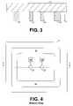
- FIG. 3is a cross-sectional view of a substrate having compliant posts and a compliant gasket formed on a surface of the substrate.
- FIG. 4is a bottom view of the substrate depicted in FIG. 3 .
- FIG. 5is a cross-sectional view of the substrate depicted in FIG. 3 after an electrically conductive layer is formed on the posts and a hermetic layer is formed on the gasket of the substrate.
- FIG. 6is a top view of a substrate to be bonded to the substrate depicted by FIG. 5 .
- FIG. 7is a cross-sectional view of the substrate depicted by FIG. 5 after spacers are formed on a surface of the substrate.
- FIG. 8is a bottom view of the substrate depicted in FIG. 7 .
- FIG. 9is a cross-sectional view of the substrate of FIG. 7 bonded with another substrate.
- FIG. 10is flow chart illustrating another exemplary method for manufacturing a device.
- FIG. 11is a cross-sectional view of a substrate having compliant posts and a compliant gasket formed on a surface of the substrate
- FIG. 12is a cross-sectional view of the substrate depicted in FIG. 11 after an electrically conductive layer is formed on the posts of the substrate.
- FIG. 13is a cross-sectional view of the substrate depicted in FIG. 12 bonded with the substrate depicted in FIG. 6 .
- FIG. 14is a cross-sectional view of the substrates depicted in FIG. 13 once a hermeticity-increasing layer is coated on an outward-facing side surface of a gasket residing between the substrates.
- FIG. 15is a top view of bonded substrates used during batch fabrication of multiple devices similar to the one depicted in FIG. 14 .
- FIG. 16is a top view of the substrates of FIG. 15 once the top substrate has been diced.
- Embodiments of the present inventiongenerally pertain to improved techniques for providing hermetic seals or electrical connections between bonded substrates.
- a compliant elemente.g., a gasket or a post
- This elementis formed of a compliant material, such as polyimide.
- At least a portion of the compliant elementis coated with a material that is selected to increase the electrical conductivity or the hermeticity of the compliant element.
- the compliant elementPrior to or during bonding, the compliant element is pressed against another substrate.
- the compliance of the elementallows it to deform and conform to the surface of the substrate. As a result, the element forms a better electrical connection or hermetic seal between the bonded substrates.
- FIG. 1depicts a device 15 manufactured in accordance with an exemplary embodiment of the present invention.
- the device 15has two substrates 21 and 24 .
- each of the substrates 21 and 24is composed of silicon.
- the substrates 21 and 24may be composed of other materials in other embodiments.
- the device 15 shown by FIG. 1has two electrically conductive posts 27 that extend between and electrically interconnect the substrates 21 and 24 . Opposite ends of each post 27 are respectively pressed against substrates 21 and 24 . Other numbers of electrically conductive posts 27 may be used in other embodiments.
- Each electrically conductive post 27is composed of a compliant material, such as polyimide or other type of compliant polymer.
- a compliant materialsuch as polyimide or other type of compliant polymer.
- Polymershave typically been used in conventional microfabricated devices as the material of stress relief layers or as a bonding material. However, polymers are generally poor conductors and have not previously been used to provide electrical connections between substrates of microfabricated devices.
- Each post 27is coated with a thin layer 33 of an electrically conductive material.
- the electrically conductive posts 27are formed on substrate 21 before the substrates 21 and 24 are bonded together.
- Electrically conductive pads 36 for contacting the electrically conductive posts 27are formed on substrate 24 .
- the pads 36complete the electrical connections between the substrates 21 and 24 by providing a relatively wide, electrically conductive area for each of the posts 27 to contact.
- the posts 27may be electrically connected to circuits residing on the substrates 21 and/or 24 .
- a gasket 42extends around the periphery of the device 15 . Opposite ends of the gasket 42 are respectively pressed against substrates 21 and 24 , and the gasket 42 provides a hermetic seal for a chamber 44 within the device 15 .
- the gasket 42is composed of a compliant material, such as polyimide or other type of compliant polymer. As described above, polymers have typically been used in conventional microfabricated devices as the material of stress relief layers or as a bonding material. However, polymers generally have poor hermetic properties and have not previously been used to form hermetic seals.
- the gasket 42is coated with a thin layer 47 of a material, such as gold, copper, glass, or silicon-nitride, that increases the hermeticity of the gasket 42 .
- a materialsuch as gold, copper, glass, or silicon-nitride
- the gasket 42can be of any shape suitable to accommodate the components that are to be located in chamber 44 (e.g., circle, square, rectangle, etc.).
- a pad 49may be formed on the substrate 24 and in contact with the gasket 42 along the gasket's entire periphery.
- the posts 27 and gasket 42are initially formed of a compliant material on the major surface of substrate 21 , as depicted by block 52 of FIG. 2 , as well as FIGS. 3 and 4 .
- Various microfabrication techniquessuch as photolithography, etching, and thermocuring, may be used to form the posts 27 and gasket 42 .
- the posts 27 and gasket 42are formed by depositing a layer of polyimide material on the substrate 21 .
- the posts 27 and gasket 42are then formed using photolithography, etching, and thermocuring.
- the posts 27are shown as having a generally circular cross-sectional shape in a plane parallel to the major surface of substrate 21 .
- the gasket 42 and posts 27may have other cross-sectional shapes in other embodiments.
- circuits 39may be formed on a surface of the substrate 21 and electrically coupled to one or more of the posts 27 .
- each of the posts 27is coated with a thin electrically conductive layer 33
- the gasket 42is coated with a thin layer 47 that increases the hermeticity of the gasket 42 .
- Various microfabrication techniquessuch as sputtering, evaporation, chemical vapor deposition (CVD), or electroplating, may be used to form the layers 33 and 47 .
- evaporation or sputteringis used to deposit a thin seed layer on the surface of the substrate 21 , including the posts 27 and gasket 42 .
- electroplatingis used to deposit a layer of electrically conductive material on the seed layer. Photolithography and etching are then used to remove the seed and electrically conductive layers from all portions of the substrate 21 except the posts 27 . As a result, a layer 33 of electrically conductive material remains on the posts 27 .
- the gasket 42with a layer 47 of gold
- evaporation or sputteringis used to deposit a thin seed layer on the surface of the substrate, including the posts 27 and gasket 42 .
- electroplatingis used to deposit gold on the seed layer.
- Photolithography and etchingare then used to remove the seed layer and the gold from all portions of the substrate 21 except the gasket 42 . As a result, a layer 47 of gold remains on the gasket 42 .
- the posts 27 and gasket 42may be used to form the posts 27 and gasket 42 , and materials other than gold may be used to form the layer 47 . If the layers 33 and 47 are composed of the same material, then these layers 33 and 47 may be formed simultaneously according to the techniques described above. In this regard, after using electroplating to deposit the material of layers 33 and 47 on the substrate 21 , photolithography and etching are used to remove such material from all portions of the substrate 21 except the posts 27 and gasket 42 .
- each of the posts 27is completely coated with the material of the layer 33
- the gasket 42is completely coated with the material of the layer 47 .
- all exposed areas of the posts 27 depicted by FIG. 4are covered with material of the layer 33
- all exposed areas of the gasket 42 depicted by FIG. 4are covered with the material of the layer 47 .
- circuits 39are indeed located on the surface of the substrate 21 , such circuits 39 may be covered with a dielectric layer or other type of insulating layer deposited on the substrate 21 before formation of the posts 27 and gasket 42 . Such a layer will protect the circuits 39 from the processes used to form the posts 27 and gasket 42 . To further protect such circuits when forming the posts 27 and gasket 42 , processes that exceed acceptable temperature ranges for the circuits should be avoided.
- FIG. 6depicts a top view of the substrate 24 .
- the substrate 24has pads 36 and 49 formed on its surface.
- the shapes of the pads 36 and 49 in the plane parallel to the major surface of substrate 24may be respectively the same as the cross-sectional shapes of the posts 27 and gasket 42 in the plane parallel to the major surfaces of substrate 21 .
- the pads 36 and 49may have shapes different from the cross-sectional shapes of the posts 27 and gasket 42 .
- circuits 51may be formed on a surface of the substrate 24 and electrically coupled to one or more of the pads 36 .
- the circuits 51are electrically coupled to the circuits 39 ( FIG. 4 ) of substrate 21 via one or more posts 27 once the substrates 21 and 24 are bonded together, as will be described in more detail hereafter.
- the substrates 21 and 24are pressed together and bonded by bonding posts 27 , gasket 42 , and/or other components of substrate 21 to substrate 24 .
- the substrates 21 and 24are aligned and pressed together such that the posts 27 contact the pads 36 and gasket 42 contacts pad 49 of substrate 24 .
- the compliance of the posts 27relieves stresses that otherwise would be present in the posts 27 and, therefore, prevents the posts 27 from fracturing or otherwise failing as the substrates 21 and 24 are being pressed together.
- pressing the substrates 21 and 24 togetherpresses the gasket 42 against the pad 49 of substrate 24 .
- the compliance of the gasket 42enables the gasket 42 to deform as the substrates 21 and 24 are pressed together.
- the deformation of the gasket 42relieves stresses that otherwise would be present in the gasket 42 and, therefore, prevents the gasket 42 from fracturing or otherwise failing as the substrates 21 and 24 are being pressed together.
- the substrates 21 and 24are bonded while being pressed together.
- Various known or future-developed bonding techniquessuch as eutectic-metal bonding, thermal compression, or gluing, may be used to bond substrates 21 and 24 .
- a eutectic-metal bondis formed between the gasket 42 and pad 49 .
- the layer 47is composed of gold (Au).
- a tin (Sn) layeris deposited on the pad 49 . Then, the substrates 21 and 24 are pressed together and heated to a temperature that melts the tin causing the tin to diffuse with the gold layer 47 . As a result, a gold-tin (Au—Sn) bond is formed between the pad 49 and the gasket 42 .
- the substrates 21 and 24may be bonded by bonding other components of the substrates 21 and 24 , such as the posts 27 or other components not specifically shown in FIG. 1 .
- the compliance of the posts 27 and the gasket 42allows each of the posts 27 and the gasket 42 to make intimate and uniform contact with the substrate 24 even if there are slight variations in the heights (measured in the y-direction) of these components or variations in the surface topology of substrate 21 or 24 .
- imperfections in the microfabrication processcause one of the posts 27 or a portion of the gasket 42 to make contact with the substrate 24 prior to another of the posts 27 or another portion of the gasket 42 , then the post 27 or gasket portion in contact with the substrate 24 will deform as the substrates 21 and 24 are pressed further together to establish contact between substrate 24 and all posts 27 and the entire periphery of the gasket 42 .
- Gasket 42may provide a hermetic seal between the substrates 21 and 24 , as described above, without there being electrically conductive connections between the substrates 21 and 24 . Further, it is possible to provide one or more electrical connections between the substrates 21 and 24 as described above without there being a gasket 42 between the substrates 21 and 24 .
- the layers 33 and 47 coating posts 27 and gasket 42may have different thicknesses depending on the material and dimensions of the posts 27 and gasket 42 .
- the gasket 42 and the posts 27should be sufficiently compliant to enable these components to deform without fracturing or otherwise mechanically failing while being pressed against the substrate 24 .
- the compliance of these componentsis generally provided by the compliant material to which the layers 33 and 47 are respectively coated.
- many types of materials that may be used to form layers 33 and 47 , respectivelyare substantially non-compliant. Thus, if the layers 33 and 47 are too thick, then the compliance of the posts 27 and the gasket 42 may be reduced to the extent that the posts 27 and gasket 42 are unable to adequately deform while being pressed against the substrate 24 .
- a fracture or other mechanical failure of the posts 27 and gasket 42may occur when the substrates 21 and 24 are pressed together. Further, a post 27 or gasket portion in one area of the device 15 may not sufficiently deform to allow another post 27 or the remainder of the gasket 42 to contact the substrate 24 .
- each electrically conductive layer 33is made significantly thinner than its corresponding post 27 .
- the layer 33is made as thin as possible consistent with providing a low-resistance electrical connection between the substrates 21 and 24 .
- the problemsare also avoided by making layer 47 significantly thinner than the gasket 42 .
- the layer 47is made as thin as possible consistent with providing a specified hermeticity for the chamber 44 .
- approximately 3-5 ⁇ m thick electrically conductive and hermetic layers 33 and 47typically achieve the foregoing.
- a suitable thickness of the layers 33 and 47may be outside of the range described above.
- the layer 47is composed of electrically conductive material (e.g., the same material as layer 33 ) such that the gasket 42 , in addition to providing a hermetic seal, also provides an electrical connection between the substrates 21 and 24 .
- the gasket 42may also be used as an electrical shield for providing electrical isolation between components in the chamber 44 and components outside of the chamber 44 .
- the posts 27 and the gasket 42are both formed on substrate 21 .
- the posts 27 and the gasket 42may be formed on different substrates, if desired.
- posts 27may be formed on substrate 21 , as described above, and the gasket 42 may be formed on substrate 24 before the two substrates 21 and 24 are pressed together and bonded.
- FIGS. 7 and 8show an embodiment in which four non-compliant spacers 68 are formed on substrate 21 .
- Other embodimentsmay have other numbers of spacers 68 .
- each of the spacers 68is located outside the periphery of the gasket 42 and, therefore, outside the chamber 44 in the example shown by FIGS. 7 and 8 , it is possible for one or more of the spacers 68 to be located inside the gasket's periphery and, therefore, in the chamber 44 in other embodiments.
- Each of the spacers 68 of FIGS. 7 and 8has the same height (measured in the y-direction), which is short enough to allow the substrate 24 to contact all of the posts 27 and gasket 42 under minimum tolerance conditions before contacting the spacers 68 .
- the spacers 68are also short enough to allow the posts 27 and gasket 42 to sufficiently deform consistent with providing low-resistance connections between the substrates 21 and 24 and a specified hermeticity for the chamber 44 , as described above.
- the spacers 68prevent the substrates 21 and 24 from moving closer together.
- the separation distance of the substrates 21 and 24precisely matches the height of the spacers 68 .
- FIG. 10depicts another exemplary method that may be used to form electrical connections and hermetic seals within devices manufactured in accordance with an embodiment of the present invention.
- the gasket 42is coated with a layer 84 of a different material after the substrates 21 and 24 are bonded.
- the componentse.g., circuits 39 and 51
- the chamber 44are not exposed and are, therefore, protected during the coating of the gasket 42 .
- posts 27 and gasket 42are formed of a compliant material on the major surface of a substrate 21 .
- each of the posts 27is coated with a layer 33 of electrically conductive material.
- the substrate 21is then pressed against another substrate 24 and bonded.
- the substrates 21 and 24are aligned and pressed together such that posts 27 contact pads 36 and gasket 42 contacts pad 49 .
- the compliance of the posts 27 and the gasket 42enables the posts 27 and the gasket 42 to deform as the substrates 21 and 24 are pressed together.
- the compliance of the posts 27 and the gasket 42helps to ensure that the entire periphery of the gasket 42 and each of the posts 27 intimately and uniformly contact components (e.g., pads 36 and 49 ) of substrate 24 during the bonding process.
- the posts 27form better electrical connections between the substrates 21 and 24
- the gasket 42forms a better hermetic seal between the substrates 21 and 24 .
- each of the coated posts 27provides an electrical connection between the substrates 21 and 24 , and the coated gasket 42 provides a hermetic seal for the chamber 44 .
- FIG. 15is a top view of substrate 21 after substrates 21 and 24 have been bonded in block 76 of FIG. 10 .
- nine gaskets 42are located between the substrates 21 and 24 and are represented with dotted lines since they are, in reality, hidden from view.
- the gaskets 42 of FIG. 15are not readily accessible for coating.
- the substrate 21is diced as shown by FIG. 16 .
- portions of the substrate 21 between the gaskets 42are removed. Therefore, while performing electroplating or CVD in block 88 of FIG. 10 , material may pass between the remaining portions of substrate 21 and coat the outward-facing side surface of each of the gaskets 42 .
- the substrate 24may then be diced to form nine separate devices 92 depicted in FIG. 14 .
Landscapes
- Engineering & Computer Science (AREA)
- Computer Hardware Design (AREA)
- Microelectronics & Electronic Packaging (AREA)
- Power Engineering (AREA)
- Manufacturing & Machinery (AREA)
- Physics & Mathematics (AREA)
- Condensed Matter Physics & Semiconductors (AREA)
- General Physics & Mathematics (AREA)
- Gasket Seals (AREA)
- Combinations Of Printed Boards (AREA)
- Internal Circuitry In Semiconductor Integrated Circuit Devices (AREA)
- Coupling Device And Connection With Printed Circuit (AREA)
Abstract
Description
Claims (20)
Priority Applications (6)
| Application Number | Priority Date | Filing Date | Title |
|---|---|---|---|
| US10/723,095US7294919B2 (en) | 2003-11-26 | 2003-11-26 | Device having a complaint element pressed between substrates |
| TW093118535ATWI357115B (en) | 2003-11-26 | 2004-06-25 | Device having a compliant element pressed between |
| JP2006541256AJP4664307B2 (en) | 2003-11-26 | 2004-11-10 | Device with compliant element pressed between substrates |
| EP04810705AEP1687845A2 (en) | 2003-11-26 | 2004-11-10 | Device having compliant electrical interconnects and compliant sealing element |
| PCT/US2004/037562WO2005055311A2 (en) | 2003-11-26 | 2004-11-10 | Device having a compliant electrical interconnects and compliant sealing element |
| CNB2004800409357ACN100444341C (en) | 2003-11-26 | 2004-11-10 | Device having a compliant electrical interconnects and compliant sealing element |
Applications Claiming Priority (1)
| Application Number | Priority Date | Filing Date | Title |
|---|---|---|---|
| US10/723,095US7294919B2 (en) | 2003-11-26 | 2003-11-26 | Device having a complaint element pressed between substrates |
Publications (2)
| Publication Number | Publication Date |
|---|---|
| US20050109455A1 US20050109455A1 (en) | 2005-05-26 |
| US7294919B2true US7294919B2 (en) | 2007-11-13 |
Family
ID=34592163
Family Applications (1)
| Application Number | Title | Priority Date | Filing Date |
|---|---|---|---|
| US10/723,095Expired - Fee RelatedUS7294919B2 (en) | 2003-11-26 | 2003-11-26 | Device having a complaint element pressed between substrates |
Country Status (6)
| Country | Link |
|---|---|
| US (1) | US7294919B2 (en) |
| EP (1) | EP1687845A2 (en) |
| JP (1) | JP4664307B2 (en) |
| CN (1) | CN100444341C (en) |
| TW (1) | TWI357115B (en) |
| WO (1) | WO2005055311A2 (en) |
Cited By (33)
| Publication number | Priority date | Publication date | Assignee | Title |
|---|---|---|---|---|
| US20080164606A1 (en)* | 2007-01-08 | 2008-07-10 | Christoffer Graae Greisen | Spacers for wafer bonding |
| US20090146531A1 (en)* | 2003-03-07 | 2009-06-11 | Ruby Richard C | Manufacturing Process For Thin Film Bulk Acoustic Resonator (FBAR) Filters |
| US20090315173A1 (en)* | 2008-06-20 | 2009-12-24 | Lucent Technologies Inc. | Heat-transfer structure |
| US7714684B2 (en) | 2004-10-01 | 2010-05-11 | Avago Technologies Wireless Ip (Singapore) Pte. Ltd. | Acoustic resonator performance enhancement using alternating frame structure |
| DE112004002038B4 (en)* | 2003-10-30 | 2010-06-02 | Avago Technologies General Ip (Singapore) Pte. Ltd. | Acoustically coupled film transformer with increased common-mode rejection |
| US7732977B2 (en) | 2008-04-30 | 2010-06-08 | Avago Technologies Wireless Ip (Singapore) | Transceiver circuit for film bulk acoustic resonator (FBAR) transducers |
| US7737807B2 (en) | 2005-10-18 | 2010-06-15 | Avago Technologies Wireless Ip (Singapore) Pte. Ltd. | Acoustic galvanic isolator incorporating series-connected decoupled stacked bulk acoustic resonators |
| US7746677B2 (en) | 2006-03-09 | 2010-06-29 | Avago Technologies Wireless Ip (Singapore) Pte. Ltd. | AC-DC converter circuit and power supply |
| US7791434B2 (en) | 2004-12-22 | 2010-09-07 | Avago Technologies Wireless Ip (Singapore) Pte. Ltd. | Acoustic resonator performance enhancement using selective metal etch and having a trench in the piezoelectric |
| US7855618B2 (en) | 2008-04-30 | 2010-12-21 | Avago Technologies Wireless Ip (Singapore) Pte. Ltd. | Bulk acoustic resonator electrical impedance transformers |
| US8080854B2 (en) | 2006-03-10 | 2011-12-20 | Avago Technologies General Ip (Singapore) Pte. Ltd. | Electronic device on substrate with cavity and mitigated parasitic leakage path |
| US8143082B2 (en) | 2004-12-15 | 2012-03-27 | Avago Technologies Wireless Ip (Singapore) Pte. Ltd. | Wafer bonding of micro-electro mechanical systems to active circuitry |
| US8193877B2 (en) | 2009-11-30 | 2012-06-05 | Avago Technologies Wireless Ip (Singapore) Pte. Ltd. | Duplexer with negative phase shifting circuit |
| US8230562B2 (en) | 2005-04-06 | 2012-07-31 | Avago Technologies Wireless Ip (Singapore) Pte. Ltd. | Method of fabricating an acoustic resonator comprising a filled recessed region |
| US8248185B2 (en) | 2009-06-24 | 2012-08-21 | Avago Technologies Wireless Ip (Singapore) Pte. Ltd. | Acoustic resonator structure comprising a bridge |
| US8350445B1 (en) | 2011-06-16 | 2013-01-08 | Avago Technologies Wireless Ip (Singapore) Pte. Ltd. | Bulk acoustic resonator comprising non-piezoelectric layer and bridge |
| US8575820B2 (en) | 2011-03-29 | 2013-11-05 | Avago Technologies General Ip (Singapore) Pte. Ltd. | Stacked bulk acoustic resonator |
| US8796904B2 (en) | 2011-10-31 | 2014-08-05 | Avago Technologies General Ip (Singapore) Pte. Ltd. | Bulk acoustic resonator comprising piezoelectric layer and inverse piezoelectric layer |
| US8902023B2 (en) | 2009-06-24 | 2014-12-02 | Avago Technologies General Ip (Singapore) Pte. Ltd. | Acoustic resonator structure having an electrode with a cantilevered portion |
| US8922302B2 (en) | 2011-08-24 | 2014-12-30 | Avago Technologies General Ip (Singapore) Pte. Ltd. | Acoustic resonator formed on a pedestal |
| US8962443B2 (en) | 2011-01-31 | 2015-02-24 | Avago Technologies General Ip (Singapore) Pte. Ltd. | Semiconductor device having an airbridge and method of fabricating the same |
| US8981876B2 (en) | 2004-11-15 | 2015-03-17 | Avago Technologies General Ip (Singapore) Pte. Ltd. | Piezoelectric resonator structures and electrical filters having frame elements |
| US9048812B2 (en) | 2011-02-28 | 2015-06-02 | Avago Technologies General Ip (Singapore) Pte. Ltd. | Bulk acoustic wave resonator comprising bridge formed within piezoelectric layer |
| US9083302B2 (en) | 2011-02-28 | 2015-07-14 | Avago Technologies General Ip (Singapore) Pte. Ltd. | Stacked bulk acoustic resonator comprising a bridge and an acoustic reflector along a perimeter of the resonator |
| US9136818B2 (en) | 2011-02-28 | 2015-09-15 | Avago Technologies General Ip (Singapore) Pte. Ltd. | Stacked acoustic resonator comprising a bridge |
| US9148117B2 (en) | 2011-02-28 | 2015-09-29 | Avago Technologies General Ip (Singapore) Pte. Ltd. | Coupled resonator filter comprising a bridge and frame elements |
| US9154112B2 (en) | 2011-02-28 | 2015-10-06 | Avago Technologies General Ip (Singapore) Pte. Ltd. | Coupled resonator filter comprising a bridge |
| US9203374B2 (en) | 2011-02-28 | 2015-12-01 | Avago Technologies General Ip (Singapore) Pte. Ltd. | Film bulk acoustic resonator comprising a bridge |
| US9243316B2 (en) | 2010-01-22 | 2016-01-26 | Avago Technologies General Ip (Singapore) Pte. Ltd. | Method of fabricating piezoelectric material with selected c-axis orientation |
| US9425764B2 (en) | 2012-10-25 | 2016-08-23 | Avago Technologies General Ip (Singapore) Pte. Ltd. | Accoustic resonator having composite electrodes with integrated lateral features |
| US9444426B2 (en) | 2012-10-25 | 2016-09-13 | Avago Technologies General Ip (Singapore) Pte. Ltd. | Accoustic resonator having integrated lateral feature and temperature compensation feature |
| US10410977B2 (en) | 2015-04-14 | 2019-09-10 | Invensas Corporation | High performance compliant substrate |
| US11032942B2 (en) | 2013-09-27 | 2021-06-08 | Alcatel Lucent | Structure for a heat transfer interface and method of manufacturing the same |
Families Citing this family (15)
| Publication number | Priority date | Publication date | Assignee | Title |
|---|---|---|---|---|
| US8143689B2 (en) | 2005-09-20 | 2012-03-27 | Bae Systems Plc | Sensor device |
| JP4834369B2 (en)* | 2005-10-07 | 2011-12-14 | ルネサスエレクトロニクス株式会社 | Semiconductor device |
| US7525398B2 (en) | 2005-10-18 | 2009-04-28 | Avago Technologies General Ip (Singapore) Pte. Ltd. | Acoustically communicating data signals across an electrical isolation barrier |
| US8193034B2 (en) | 2006-11-10 | 2012-06-05 | Stats Chippac, Ltd. | Semiconductor device and method of forming vertical interconnect structure using stud bumps |
| US8174119B2 (en) | 2006-11-10 | 2012-05-08 | Stats Chippac, Ltd. | Semiconductor package with embedded die |
| US8133762B2 (en)* | 2009-03-17 | 2012-03-13 | Stats Chippac, Ltd. | Semiconductor device and method of providing z-interconnect conductive pillars with inner polymer core |
| US7530814B2 (en)* | 2007-09-25 | 2009-05-12 | Intel Corporation | Providing variable sized contacts for coupling with a semiconductor device |
| US8618670B2 (en)* | 2008-08-15 | 2013-12-31 | Qualcomm Incorporated | Corrosion control of stacked integrated circuits |
| JP6342033B2 (en)* | 2010-06-30 | 2018-06-13 | キヤノン株式会社 | Solid-state imaging device |
| JP5505171B2 (en)* | 2010-07-30 | 2014-05-28 | 富士通株式会社 | Circuit board unit, circuit board unit manufacturing method, and electronic apparatus |
| JP5704231B2 (en)* | 2011-04-11 | 2015-04-22 | 株式会社村田製作所 | Electronic component and method for manufacturing electronic component |
| JP5984912B2 (en)* | 2012-03-23 | 2016-09-06 | オリンパス株式会社 | Manufacturing method of stacked semiconductor |
| US9373585B2 (en) | 2014-09-17 | 2016-06-21 | Invensas Corporation | Polymer member based interconnect |
| US11600573B2 (en)* | 2019-06-26 | 2023-03-07 | Taiwan Semiconductor Manufacturing Co., Ltd. | Structure and formation method of chip package with conductive support elements to reduce warpage |
| CN114664747B (en)* | 2020-12-31 | 2023-02-03 | 华为技术有限公司 | Board-level structure and communication equipment |
Citations (26)
| Publication number | Priority date | Publication date | Assignee | Title |
|---|---|---|---|---|
| US3967162A (en)* | 1974-07-24 | 1976-06-29 | Amp Incorporated | Interconnection of oppositely disposed circuit devices |
| US4116517A (en)* | 1976-04-15 | 1978-09-26 | International Telephone And Telegraph Corporation | Flexible printed circuit and electrical connection therefor |
| US4769272A (en) | 1987-03-17 | 1988-09-06 | National Semiconductor Corporation | Ceramic lid hermetic seal package structure |
| EP0295914A2 (en) | 1987-06-19 | 1988-12-21 | Hewlett-Packard Company | An interconnect structure for PC boards and integrated circuits |
| US4857668A (en)* | 1988-04-15 | 1989-08-15 | Schlegel Corporation | Multi-function gasket |
| US5142101A (en)* | 1990-11-29 | 1992-08-25 | Kitagawa Industries Co., Ltd. | Electromagnetic-shielding gasket |
| JPH05243231A (en) | 1992-03-03 | 1993-09-21 | Matsushita Electric Ind Co Ltd | Electronic part mounting connecting body and manufacture thereof |
| US5262347A (en) | 1991-08-14 | 1993-11-16 | Bell Communications Research, Inc. | Palladium welding of a semiconductor body |
| US5397857A (en)* | 1993-07-15 | 1995-03-14 | Dual Systems | PCMCIA standard memory card frame |
| US5474458A (en)* | 1993-07-13 | 1995-12-12 | Fujitsu Limited | Interconnect carriers having high-density vertical connectors and methods for making the same |
| US5508228A (en) | 1994-02-14 | 1996-04-16 | Microelectronics And Computer Technology Corporation | Compliant electrically connective bumps for an adhesive flip chip integrated circuit device and methods for forming same |
| US5835142A (en) | 1992-02-04 | 1998-11-10 | Matsushita Electric Industrial Co., Ltd. | Direct contact type image sensor and its production method |
| US5854514A (en)* | 1996-08-05 | 1998-12-29 | International Buisness Machines Corporation | Lead-free interconnection for electronic devices |
| US5938452A (en)* | 1996-12-23 | 1999-08-17 | General Electric Company | Flexible interface structures for electronic devices |
| US6046410A (en)* | 1996-12-23 | 2000-04-04 | General Electric Company | Interface structures for electronic devices |
| US6090687A (en) | 1998-07-29 | 2000-07-18 | Agilent Technolgies, Inc. | System and method for bonding and sealing microfabricated wafers to form a single structure having a vacuum chamber therein |
| US6096413A (en)* | 1993-09-10 | 2000-08-01 | Chomerics, Inc. | Form-in-place EMI gaskets |
| US6118181A (en) | 1998-07-29 | 2000-09-12 | Agilent Technologies, Inc. | System and method for bonding wafers |
| US6249051B1 (en) | 1994-05-06 | 2001-06-19 | Industrial Technology Research Institute | Composite bump flip chip bonding |
| US6266872B1 (en)* | 1996-12-12 | 2001-07-31 | Tessera, Inc. | Method for making a connection component for a semiconductor chip package |
| US6358063B1 (en)* | 2000-06-28 | 2002-03-19 | Intercon Systems, Inc. | Sealed interposer assembly |
| US6365500B1 (en) | 1994-05-06 | 2002-04-02 | Industrial Technology Research Institute | Composite bump bonding |
| US6451374B1 (en)* | 2000-02-18 | 2002-09-17 | Parker-Hannifin Corporation | Manufacture of low closure force, form-in-place EMI shielding gasket |
| US6580159B1 (en) | 1999-11-05 | 2003-06-17 | Amkor Technology, Inc. | Integrated circuit device packages and substrates for making the packages |
| US6713314B2 (en)* | 2002-08-14 | 2004-03-30 | Intel Corporation | Hermetically packaging a microelectromechanical switch and a film bulk acoustic resonator |
| US7005573B2 (en)* | 2003-02-13 | 2006-02-28 | Parker-Hannifin Corporation | Composite EMI shield |
Family Cites Families (2)
| Publication number | Priority date | Publication date | Assignee | Title |
|---|---|---|---|---|
| JPH0349246A (en)* | 1989-07-17 | 1991-03-04 | Hitachi Ltd | Semiconductor integrated circuit device |
| JPH1167829A (en)* | 1997-08-22 | 1999-03-09 | Oki Electric Ind Co Ltd | Method for mounting electronic component, and electronic component and wiring board used in the method |
- 2003
- 2003-11-26USUS10/723,095patent/US7294919B2/ennot_activeExpired - Fee Related
- 2004
- 2004-06-25TWTW093118535Apatent/TWI357115B/ennot_activeIP Right Cessation
- 2004-11-10EPEP04810705Apatent/EP1687845A2/ennot_activeWithdrawn
- 2004-11-10CNCNB2004800409357Apatent/CN100444341C/ennot_activeExpired - Fee Related
- 2004-11-10JPJP2006541256Apatent/JP4664307B2/ennot_activeExpired - Fee Related
- 2004-11-10WOPCT/US2004/037562patent/WO2005055311A2/enactiveApplication Filing
Patent Citations (28)
| Publication number | Priority date | Publication date | Assignee | Title |
|---|---|---|---|---|
| US3967162A (en)* | 1974-07-24 | 1976-06-29 | Amp Incorporated | Interconnection of oppositely disposed circuit devices |
| US4116517A (en)* | 1976-04-15 | 1978-09-26 | International Telephone And Telegraph Corporation | Flexible printed circuit and electrical connection therefor |
| US4769272A (en) | 1987-03-17 | 1988-09-06 | National Semiconductor Corporation | Ceramic lid hermetic seal package structure |
| EP0295914A2 (en) | 1987-06-19 | 1988-12-21 | Hewlett-Packard Company | An interconnect structure for PC boards and integrated circuits |
| US4857668A (en)* | 1988-04-15 | 1989-08-15 | Schlegel Corporation | Multi-function gasket |
| US5142101A (en)* | 1990-11-29 | 1992-08-25 | Kitagawa Industries Co., Ltd. | Electromagnetic-shielding gasket |
| US5262347A (en) | 1991-08-14 | 1993-11-16 | Bell Communications Research, Inc. | Palladium welding of a semiconductor body |
| US5835142A (en) | 1992-02-04 | 1998-11-10 | Matsushita Electric Industrial Co., Ltd. | Direct contact type image sensor and its production method |
| JPH05243231A (en) | 1992-03-03 | 1993-09-21 | Matsushita Electric Ind Co Ltd | Electronic part mounting connecting body and manufacture thereof |
| US5474458A (en)* | 1993-07-13 | 1995-12-12 | Fujitsu Limited | Interconnect carriers having high-density vertical connectors and methods for making the same |
| US5397857A (en)* | 1993-07-15 | 1995-03-14 | Dual Systems | PCMCIA standard memory card frame |
| US6096413A (en)* | 1993-09-10 | 2000-08-01 | Chomerics, Inc. | Form-in-place EMI gaskets |
| US5508228A (en) | 1994-02-14 | 1996-04-16 | Microelectronics And Computer Technology Corporation | Compliant electrically connective bumps for an adhesive flip chip integrated circuit device and methods for forming same |
| US6365500B1 (en) | 1994-05-06 | 2002-04-02 | Industrial Technology Research Institute | Composite bump bonding |
| US6249051B1 (en) | 1994-05-06 | 2001-06-19 | Industrial Technology Research Institute | Composite bump flip chip bonding |
| US6005292A (en)* | 1996-08-05 | 1999-12-21 | International Business Machines Corporation | Lead-free interconnection for electronic devices |
| US5854514A (en)* | 1996-08-05 | 1998-12-29 | International Buisness Machines Corporation | Lead-free interconnection for electronic devices |
| US6266872B1 (en)* | 1996-12-12 | 2001-07-31 | Tessera, Inc. | Method for making a connection component for a semiconductor chip package |
| US6092280A (en)* | 1996-12-23 | 2000-07-25 | General Electric Co. | Flexible interface structures for electronic devices |
| US6046410A (en)* | 1996-12-23 | 2000-04-04 | General Electric Company | Interface structures for electronic devices |
| US5938452A (en)* | 1996-12-23 | 1999-08-17 | General Electric Company | Flexible interface structures for electronic devices |
| US6090687A (en) | 1998-07-29 | 2000-07-18 | Agilent Technolgies, Inc. | System and method for bonding and sealing microfabricated wafers to form a single structure having a vacuum chamber therein |
| US6118181A (en) | 1998-07-29 | 2000-09-12 | Agilent Technologies, Inc. | System and method for bonding wafers |
| US6580159B1 (en) | 1999-11-05 | 2003-06-17 | Amkor Technology, Inc. | Integrated circuit device packages and substrates for making the packages |
| US6451374B1 (en)* | 2000-02-18 | 2002-09-17 | Parker-Hannifin Corporation | Manufacture of low closure force, form-in-place EMI shielding gasket |
| US6358063B1 (en)* | 2000-06-28 | 2002-03-19 | Intercon Systems, Inc. | Sealed interposer assembly |
| US6713314B2 (en)* | 2002-08-14 | 2004-03-30 | Intel Corporation | Hermetically packaging a microelectromechanical switch and a film bulk acoustic resonator |
| US7005573B2 (en)* | 2003-02-13 | 2006-02-28 | Parker-Hannifin Corporation | Composite EMI shield |
Non-Patent Citations (1)
| Title |
|---|
| Larson, et al., U.S. Appl. No. 10/890,343 entitled, "A Film Bulk Acoustic Resonator Package and Method of Fabricating Same," filed Jul. 13, 2004. |
Cited By (39)
| Publication number | Priority date | Publication date | Assignee | Title |
|---|---|---|---|---|
| US7802349B2 (en) | 2003-03-07 | 2010-09-28 | Avago Technologies Wireless Ip (Singapore) Pte. Ltd. | Manufacturing process for thin film bulk acoustic resonator (FBAR) filters |
| US20090146531A1 (en)* | 2003-03-07 | 2009-06-11 | Ruby Richard C | Manufacturing Process For Thin Film Bulk Acoustic Resonator (FBAR) Filters |
| DE112004002038B4 (en)* | 2003-10-30 | 2010-06-02 | Avago Technologies General Ip (Singapore) Pte. Ltd. | Acoustically coupled film transformer with increased common-mode rejection |
| US7714684B2 (en) | 2004-10-01 | 2010-05-11 | Avago Technologies Wireless Ip (Singapore) Pte. Ltd. | Acoustic resonator performance enhancement using alternating frame structure |
| US8981876B2 (en) | 2004-11-15 | 2015-03-17 | Avago Technologies General Ip (Singapore) Pte. Ltd. | Piezoelectric resonator structures and electrical filters having frame elements |
| US8143082B2 (en) | 2004-12-15 | 2012-03-27 | Avago Technologies Wireless Ip (Singapore) Pte. Ltd. | Wafer bonding of micro-electro mechanical systems to active circuitry |
| US8188810B2 (en) | 2004-12-22 | 2012-05-29 | Avago Technologies Wireless Ip (Singapore) Pte. Ltd. | Acoustic resonator performance enhancement using selective metal etch |
| US7791434B2 (en) | 2004-12-22 | 2010-09-07 | Avago Technologies Wireless Ip (Singapore) Pte. Ltd. | Acoustic resonator performance enhancement using selective metal etch and having a trench in the piezoelectric |
| US8230562B2 (en) | 2005-04-06 | 2012-07-31 | Avago Technologies Wireless Ip (Singapore) Pte. Ltd. | Method of fabricating an acoustic resonator comprising a filled recessed region |
| US7737807B2 (en) | 2005-10-18 | 2010-06-15 | Avago Technologies Wireless Ip (Singapore) Pte. Ltd. | Acoustic galvanic isolator incorporating series-connected decoupled stacked bulk acoustic resonators |
| US8238129B2 (en) | 2006-03-09 | 2012-08-07 | Avago Technologies Wireless Ip (Singapore) Pte. Ltd. | AC-DC converter circuit and power supply |
| US7746677B2 (en) | 2006-03-09 | 2010-06-29 | Avago Technologies Wireless Ip (Singapore) Pte. Ltd. | AC-DC converter circuit and power supply |
| US8080854B2 (en) | 2006-03-10 | 2011-12-20 | Avago Technologies General Ip (Singapore) Pte. Ltd. | Electronic device on substrate with cavity and mitigated parasitic leakage path |
| US20080164606A1 (en)* | 2007-01-08 | 2008-07-10 | Christoffer Graae Greisen | Spacers for wafer bonding |
| US7732977B2 (en) | 2008-04-30 | 2010-06-08 | Avago Technologies Wireless Ip (Singapore) | Transceiver circuit for film bulk acoustic resonator (FBAR) transducers |
| US7855618B2 (en) | 2008-04-30 | 2010-12-21 | Avago Technologies Wireless Ip (Singapore) Pte. Ltd. | Bulk acoustic resonator electrical impedance transformers |
| US20090315173A1 (en)* | 2008-06-20 | 2009-12-24 | Lucent Technologies Inc. | Heat-transfer structure |
| US9308571B2 (en) | 2008-06-20 | 2016-04-12 | Alcatel Lucent | Heat-transfer structure |
| US8963323B2 (en)* | 2008-06-20 | 2015-02-24 | Alcatel Lucent | Heat-transfer structure |
| US8248185B2 (en) | 2009-06-24 | 2012-08-21 | Avago Technologies Wireless Ip (Singapore) Pte. Ltd. | Acoustic resonator structure comprising a bridge |
| US8902023B2 (en) | 2009-06-24 | 2014-12-02 | Avago Technologies General Ip (Singapore) Pte. Ltd. | Acoustic resonator structure having an electrode with a cantilevered portion |
| US8193877B2 (en) | 2009-11-30 | 2012-06-05 | Avago Technologies Wireless Ip (Singapore) Pte. Ltd. | Duplexer with negative phase shifting circuit |
| US9243316B2 (en) | 2010-01-22 | 2016-01-26 | Avago Technologies General Ip (Singapore) Pte. Ltd. | Method of fabricating piezoelectric material with selected c-axis orientation |
| US9859205B2 (en) | 2011-01-31 | 2018-01-02 | Avago Technologies General Ip (Singapore) Pte. Ltd. | Semiconductor device having an airbridge and method of fabricating the same |
| US8962443B2 (en) | 2011-01-31 | 2015-02-24 | Avago Technologies General Ip (Singapore) Pte. Ltd. | Semiconductor device having an airbridge and method of fabricating the same |
| US9083302B2 (en) | 2011-02-28 | 2015-07-14 | Avago Technologies General Ip (Singapore) Pte. Ltd. | Stacked bulk acoustic resonator comprising a bridge and an acoustic reflector along a perimeter of the resonator |
| US9136818B2 (en) | 2011-02-28 | 2015-09-15 | Avago Technologies General Ip (Singapore) Pte. Ltd. | Stacked acoustic resonator comprising a bridge |
| US9148117B2 (en) | 2011-02-28 | 2015-09-29 | Avago Technologies General Ip (Singapore) Pte. Ltd. | Coupled resonator filter comprising a bridge and frame elements |
| US9154112B2 (en) | 2011-02-28 | 2015-10-06 | Avago Technologies General Ip (Singapore) Pte. Ltd. | Coupled resonator filter comprising a bridge |
| US9203374B2 (en) | 2011-02-28 | 2015-12-01 | Avago Technologies General Ip (Singapore) Pte. Ltd. | Film bulk acoustic resonator comprising a bridge |
| US9048812B2 (en) | 2011-02-28 | 2015-06-02 | Avago Technologies General Ip (Singapore) Pte. Ltd. | Bulk acoustic wave resonator comprising bridge formed within piezoelectric layer |
| US8575820B2 (en) | 2011-03-29 | 2013-11-05 | Avago Technologies General Ip (Singapore) Pte. Ltd. | Stacked bulk acoustic resonator |
| US8350445B1 (en) | 2011-06-16 | 2013-01-08 | Avago Technologies Wireless Ip (Singapore) Pte. Ltd. | Bulk acoustic resonator comprising non-piezoelectric layer and bridge |
| US8922302B2 (en) | 2011-08-24 | 2014-12-30 | Avago Technologies General Ip (Singapore) Pte. Ltd. | Acoustic resonator formed on a pedestal |
| US8796904B2 (en) | 2011-10-31 | 2014-08-05 | Avago Technologies General Ip (Singapore) Pte. Ltd. | Bulk acoustic resonator comprising piezoelectric layer and inverse piezoelectric layer |
| US9444426B2 (en) | 2012-10-25 | 2016-09-13 | Avago Technologies General Ip (Singapore) Pte. Ltd. | Accoustic resonator having integrated lateral feature and temperature compensation feature |
| US9425764B2 (en) | 2012-10-25 | 2016-08-23 | Avago Technologies General Ip (Singapore) Pte. Ltd. | Accoustic resonator having composite electrodes with integrated lateral features |
| US11032942B2 (en) | 2013-09-27 | 2021-06-08 | Alcatel Lucent | Structure for a heat transfer interface and method of manufacturing the same |
| US10410977B2 (en) | 2015-04-14 | 2019-09-10 | Invensas Corporation | High performance compliant substrate |
Also Published As
| Publication number | Publication date |
|---|---|
| EP1687845A2 (en) | 2006-08-09 |
| WO2005055311A2 (en) | 2005-06-16 |
| CN1906744A (en) | 2007-01-31 |
| WO2005055311A3 (en) | 2005-07-28 |
| CN100444341C (en) | 2008-12-17 |
| JP4664307B2 (en) | 2011-04-06 |
| JP2007512707A (en) | 2007-05-17 |
| TWI357115B (en) | 2012-01-21 |
| TW200518241A (en) | 2005-06-01 |
| US20050109455A1 (en) | 2005-05-26 |
Similar Documents
| Publication | Publication Date | Title |
|---|---|---|
| US7294919B2 (en) | Device having a complaint element pressed between substrates | |
| US6376280B1 (en) | Microcap wafer-level package | |
| JP4420538B2 (en) | Wafer package manufacturing method | |
| US6450039B1 (en) | Pressure sensor and method of manufacturing the same | |
| US4494688A (en) | Method of connecting metal leads with electrodes of semiconductor device and metal lead therefore | |
| US4873615A (en) | Semiconductor chip carrier system | |
| US20070275495A1 (en) | Method for fabricating a pressure sensor using SOI wafers | |
| WO2007076099A2 (en) | Microelectronic elements with compliant terminal mountings and methods for making the same | |
| US5264075A (en) | Fabrication methods for silicon/glass capacitive absolute pressure sensors | |
| JP2011131309A5 (en) | Semiconductor package manufacturing method and semiconductor package | |
| US20030122237A1 (en) | Semiconductor device | |
| KR100323194B1 (en) | Semiconductor device and manufacturing method thereof | |
| US7737513B2 (en) | Chip assembly including package element and integrated circuit chip | |
| US20060033189A1 (en) | Structure and method of forming capped chips | |
| EP1465250A1 (en) | Insulated power semiconductor module with reduced partial discharge and manufacturing method | |
| US20060049527A1 (en) | Electronic device and method of manufacturing the same | |
| EP1199744B1 (en) | Microcap wafer-level package | |
| JPS594853B2 (en) | semiconductor equipment | |
| TWI588954B (en) | Chip package and manufacturing method thereof | |
| JP6712136B2 (en) | Electronic component manufacturing method | |
| US6756138B1 (en) | Micro-electromechanical devices | |
| US20220301996A1 (en) | Spacers formed on a substrate with etched micro-springs | |
| JP3434918B2 (en) | Semiconductor device | |
| CN118866706A (en) | Method for manufacturing semiconductor structure | |
| JPH11176859A (en) | Electrode structure for semiconductor device and manufacture of the electrode structure for the semiconductor device |
Legal Events
| Date | Code | Title | Description |
|---|---|---|---|
| AS | Assignment | Owner name:AGILENT TECHNOLOGIES, INC., COLORADO Free format text:ASSIGNMENT OF ASSIGNORS INTEREST;ASSIGNOR:BAI, QING;REEL/FRAME:014563/0439 Effective date:20031126 | |
| AS | Assignment | Owner name:AVAGO TECHNOLOGIES GENERAL IP PTE. LTD.,SINGAPORE Free format text:ASSIGNMENT OF ASSIGNORS INTEREST;ASSIGNOR:AGILENT TECHNOLOGIES, INC.;REEL/FRAME:017206/0666 Effective date:20051201 Owner name:AVAGO TECHNOLOGIES GENERAL IP PTE. LTD., SINGAPORE Free format text:ASSIGNMENT OF ASSIGNORS INTEREST;ASSIGNOR:AGILENT TECHNOLOGIES, INC.;REEL/FRAME:017206/0666 Effective date:20051201 | |
| CC | Certificate of correction | ||
| FPAY | Fee payment | Year of fee payment:4 | |
| REMI | Maintenance fee reminder mailed | ||
| LAPS | Lapse for failure to pay maintenance fees | ||
| STCH | Information on status: patent discontinuation | Free format text:PATENT EXPIRED DUE TO NONPAYMENT OF MAINTENANCE FEES UNDER 37 CFR 1.362 | |
| FP | Expired due to failure to pay maintenance fee | Effective date:20151113 | |
| AS | Assignment | Owner name:AVAGO TECHNOLOGIES GENERAL IP (SINGAPORE) PTE. LTD Free format text:CORRECTIVE ASSIGNMENT TO CORRECT THE ASSIGNEE NAME PREVIOUSLY RECORDED AT REEL: 017206 FRAME: 0666. ASSIGNOR(S) HEREBY CONFIRMS THE ASSIGNMENT;ASSIGNOR:AGILENT TECHNOLOGIES, INC.;REEL/FRAME:038632/0662 Effective date:20051201 |