US7294542B2 - Method of fabricating a semiconductor device having CMOS transistors and a bipolar transistor - Google Patents
Method of fabricating a semiconductor device having CMOS transistors and a bipolar transistorDownload PDFInfo
- Publication number
- US7294542B2 US7294542B2US11/442,288US44228806AUS7294542B2US 7294542 B2US7294542 B2US 7294542B2US 44228806 AUS44228806 AUS 44228806AUS 7294542 B2US7294542 B2US 7294542B2
- Authority
- US
- United States
- Prior art keywords
- type
- bipolar transistor
- layer
- esd protection
- diode
- Prior art date
- Legal status (The legal status is an assumption and is not a legal conclusion. Google has not performed a legal analysis and makes no representation as to the accuracy of the status listed.)
- Expired - Fee Related
Links
Images


Classifications
- H—ELECTRICITY
- H10—SEMICONDUCTOR DEVICES; ELECTRIC SOLID-STATE DEVICES NOT OTHERWISE PROVIDED FOR
- H10D—INORGANIC ELECTRIC SEMICONDUCTOR DEVICES
- H10D84/00—Integrated devices formed in or on semiconductor substrates that comprise only semiconducting layers, e.g. on Si wafers or on GaAs-on-Si wafers
- H—ELECTRICITY
- H10—SEMICONDUCTOR DEVICES; ELECTRIC SOLID-STATE DEVICES NOT OTHERWISE PROVIDED FOR
- H10D—INORGANIC ELECTRIC SEMICONDUCTOR DEVICES
- H10D89/00—Aspects of integrated devices not covered by groups H10D84/00 - H10D88/00
- H10D89/60—Integrated devices comprising arrangements for electrical or thermal protection, e.g. protection circuits against electrostatic discharge [ESD]
- H10D89/601—Integrated devices comprising arrangements for electrical or thermal protection, e.g. protection circuits against electrostatic discharge [ESD] for devices having insulated gate electrodes, e.g. for IGFETs or IGBTs
- H10D89/711—Integrated devices comprising arrangements for electrical or thermal protection, e.g. protection circuits against electrostatic discharge [ESD] for devices having insulated gate electrodes, e.g. for IGFETs or IGBTs using bipolar transistors as protective elements
- H—ELECTRICITY
- H10—SEMICONDUCTOR DEVICES; ELECTRIC SOLID-STATE DEVICES NOT OTHERWISE PROVIDED FOR
- H10D—INORGANIC ELECTRIC SEMICONDUCTOR DEVICES
- H10D89/00—Aspects of integrated devices not covered by groups H10D84/00 - H10D88/00
- H10D89/60—Integrated devices comprising arrangements for electrical or thermal protection, e.g. protection circuits against electrostatic discharge [ESD]
- H10D89/601—Integrated devices comprising arrangements for electrical or thermal protection, e.g. protection circuits against electrostatic discharge [ESD] for devices having insulated gate electrodes, e.g. for IGFETs or IGBTs
- H10D89/611—Integrated devices comprising arrangements for electrical or thermal protection, e.g. protection circuits against electrostatic discharge [ESD] for devices having insulated gate electrodes, e.g. for IGFETs or IGBTs using diodes as protective elements
- H—ELECTRICITY
- H01—ELECTRIC ELEMENTS
- H01L—SEMICONDUCTOR DEVICES NOT COVERED BY CLASS H10
- H01L2924/00—Indexing scheme for arrangements or methods for connecting or disconnecting semiconductor or solid-state bodies as covered by H01L24/00
- H01L2924/0001—Technical content checked by a classifier
- H01L2924/0002—Not covered by any one of groups H01L24/00, H01L24/00 and H01L2224/00
Definitions
- the present inventionrelates to an ESD protection apparatus to be installed in a semiconductor integrated circuit chip in order to protect a semiconductor integrated circuit from electrostatic discharge (ESD) and to a method for fabricating the protection apparatus.
- ESDelectrostatic discharge
- a conventional ESD protection apparatus in the CMOS processgenerally protects a semiconductor integrated circuit using a MOSFET transverse parasitic bipolar transistor by releasing the electric current in the transverse direction lateral direction in a silicon substrate.
- the ESD protection apparatushas been required to be further miniaturized since the number of pins to be mounted on one chip has been increased sharply following the recent acute requirement of development of semiconductor integrated circuits made finer.
- the present inventionaims to provide an ESD protection apparatus in which electric current concentration and electric field concentration upon the junction parts hardly take place even if miniaturization is advanced and which is capable of triggering at a lower voltage and to provide a method for fabricating such an ESD protection apparatus.
- the ESD protection apparatus of the present inventionis to be installed between a pad of a semiconductor integrated circuit chip and an inner circuit of the semiconductor integrated circuit chip.
- the ESD protection apparatusis provided with a trigger element comprising a diode to be broken down by overvoltage applied to the pad and an ESD protection element comprising a longitudinal bipolar transistor also known in the art as a vertical bipolar transistor for discharging the accumulated electric charge of the pad by being electrically discharged attributed to the breakdown of the diode.
- a longitudinal bipolar transistorAs compared with a transverse bipolar transistor, a longitudinal bipolar transistor has a wide junction surface area for the same occupancy surface area, so that even if miniaturization is promoted, the electric current concentration and the electric field concentration hardly take place.
- a diodeis easy to set a desired breakdown voltage by changing the impurity concentration. Consequently, an ESD protection apparatus in which electric current concentration and electric field concentration upon the junction parts hardly take place even if miniaturization is advanced and which is capable of triggering at a lower voltage can be obtained by utilizing the breakdown voltage of a diode for the trigger of a longitudinal bipolar transistor.
- a first practical example of an ESD protection apparatus of the present inventionis as follows.
- the padis an input terminal or an output terminal.
- the trigger elementcomprises a first and a second diodes and a first and a second resistors.
- the ESD protection elementcomprises NPN type first and second longitudinal bipolar transistors.
- the cathodeis connected with the pad and the anode is connected with the base of the first longitudinal bipolar transistor.
- the cathodeis connected with an electric power source terminal and the anode is connected with the base of the second longitudinal bipolar transistor.
- the first resistoris connected between the anode of the first diode and the ground terminal.
- the second resistoris connected between the anode of the second diode and the pad.
- the collectoris connected with the pad and the emitter is connected with the ground terminal.
- the collectoris connected with the electric power source terminal and the emitter is connected with the pad.
- at least either of a first diode, a first resistor and a first longitudinal bipolar transistor or a second diode, a second resistor and a second longitudinal bipolar transistormay be provided.
- a second practical example of an ESD protection apparatus of the present inventionis as follows.
- the padis an electric power source terminal.
- the longitudinal bipolar transistoris NPN type.
- the diodethe cathode is connected with the pad and the anode is connected with the base of the longitudinal bipolar transistor.
- a resistoris connected between the anode of the diode and a ground terminal.
- the longitudinal bipolar transistorthe collector is connected with the pad and the emitter is connected with the ground terminal.
- An ESD protection apparatus of the present inventionmay has the following constitution.
- the trigger elementcomprises, as a diode to be broken down by overvoltage applied to the pad, a first longitudinal bipolar transistor whose collector and base work and which discharges the accumulated electric charge of the pad by being electrically communicated attributed to the breakdown of the diode.
- the ESD protection elementcomprises a second longitudinal bipolar transistor for discharging the accumulated electric charge of the pad by being electrically communicated attributed to the breakdown of the diode.
- the padis an input terminal or an output terminal.
- the trigger elementcomprises an NPN type longitudinal bipolar transistor A and an NPN longitudinal bipolar transistor B working as the first longitudinal bipolar transistor and a first and a second resistors.
- the ESD protection elementcomprises an NPN type longitudinal bipolar transistor C and an NPN type longitudinal bipolar transistor D working as the second longitudinal bipolar transistor.
- the collectorsare connected with the pad and the bases are connected with each other and the emitters are connected with a ground terminal.
- the first resistoris connected between the bases of the longitudinal bipolar transistors A, C and the ground terminal.
- the collectorsare connected with an electric power source terminal and the bases are connected with each other and the emitters are connected with the pad.
- the second resistoris connected between the bases of the longitudinal bipolar transistors B, D and the pad.
- the padis an electric power source terminal.
- the first and second longitudinal bipolar transistorsare NPN type and their collectors are connected with the pad and their bases are connected with each other and their emitters are connected with a ground terminal.
- a resistoris connected between the bases of the first and second longitudinal bipolar transistors and the ground terminal.
- the conductive types P and Nmay be taken as reverse conductive types N and P, respectively. Even if the P and the N are reversed, the kind of a carrier alone is changed and naturally the same function can be realized. Incidentally, when the longitudinal bipolar transistor is taken as PNP type, the positions of the diode and the resistor are replaced with each other.
- the diodemay comprise a single diode or plural diodes connected in series, the overvoltage may be an forward voltage for the diode and the breakdown may be a substantial breakdown by being electrically discharged.
- the diode forward descending voltageis, compared with the breakdown voltage, hard to depend on high impurity concentration and a low voltage. Consequently, by selecting the number of diodes to be connected in series, a desired substantial breakdown voltage can be accurately set.
- the collector layers of the above described first longitudinal bipolar transistor and the above described second longitudinal bipolar transistormay be as simultaneously formed.
- the above described first longitudinal bipolar transistor and the above described second longitudinal bipolar transistormay have a common collector layer.
- the longitudinal bipolar transistor or the diodecomprises all or some of: a first N ⁇ type well formed on the P type silicon substrate surface; a second N ⁇ type well adjacent to this first N ⁇ type well and formed on the P type silicon substrate surface; a second N + layer formed on this second N ⁇ type well surface; the P ⁇ type well formed on the first N ⁇ type well surface; the P + layer and a first N + layer formed on this P ⁇ type well surface apart from each other; the insulation material installed between these P + layer and the first N + layer for preventing the electric connection with the P + layer and the first N + layer, wherein the second N ⁇ type well and the P ⁇ type well may be insulated by the insulation material for isolation and the P type silicon substrate and the P ⁇ type well may be insulated by the insulation material for isolation.
- the conductive type P and Nmay be taken as the reverse conductive N and P, respectively.
- the P + layer and the first and second N + layersmay be formed simultaneously with the P + layer and the N + layer of the CMOS transistor constituting the inner circuit.
- a second N ⁇ type wellmay be formed simultaneously with the N ⁇ type well of the CMOS transistor constituting the inner circuit.
- the insulation materialmay be a dummy gate or a mere insulation material formed simultaneously formed with the gate electrode and the gate insulation film of the CMOS transistor constituting the inner circuit.
- This dummy electrode or the insulation filmmay be formed in a ring shape on the silicon substrate surface.
- the diodemay comprises: the N ⁇ type well formed on the P type silicon substrate surface; the P + layer and the N + layer formed on the N ⁇ type well surface apart from each other; and the insulation material formed in the inside from the above described P type silicon substrate surface between these P + layer and N + layer.
- the conductive type P and Nmay be the reverse conductive type N and P, respectively.
- the diodecomprises: the N ⁇ type well formed on the P type silicon substrate surface; the P ⁇ type well formed on this N ⁇ type well surface; the P + layer and the N + layer formed on this P ⁇ type well surface apart from each other; and the insulation material installed on the P type silicon substrate surface between these P + layer and N + layer, wherein the P type silicon substrate and the P ⁇ type well may be insulated by the insulation material for isolation.
- the conductive type P and Nmay be taken as the reverse conductive type N and P, respectively.
- An ESD protection apparatus of the present inventionmay further have the following constitution.
- the diodecomprises a P ⁇ type well formed on the surface of a silicon substrate, an N + type layer and a P + type layer formed on the P ⁇ type well surface at an interval from each other, and a dummy gate electrode formed on the P ⁇ type well via an insulation film and between the N + type layer and the P + type layer and connected with a ground terminal.
- the electric field between the N + layer and the dummy gate electrodeis intensified, the ESD trigger at a lower voltage.
- the conductive type P and Nmay be the reverse conductive type N and P, respectively.
- a method for fabricating an ESD protection apparatus relevant to the present inventionis a method for fabricating an ESD protection apparatus according to claim 1 and comprises the following steps. (1) A first step of simultaneously forming an N ⁇ type well of a CMOS transistor composing the inner circuit and an N ⁇ type well for connector connection to be connected with the collector of the longitudinal bipolar transistor on a P type silicon substrate. (2) A second step of simultaneously forming a collector N ⁇ type well to be a collector of the longitudinal bipolar transistor and an N ⁇ type well of the diode on the P type silicon substrate.
- the method for fabricating the ESD protection apparatus according to the inventionallows the anode and the cathode to be reversed.
- An ESD protection apparatus relevant to the present inventioncan be fabricated simultaneously in the fabrication process of a CMOS transistor except the steps (2) and (3). Since the steps (2) and (3) comprise ion implantation in the same parts, required is only one sheet of mask to be added in the conventional CMOS transistor fabrication process.
- the ESD protection apparatus fabrication methodmay further comprise a step of forming a dummy gate electrode simultaneously with a gate electrode of the CMOS transistor in the region where the collector N ⁇ type well of the longitudinal bipolar transistor and N ⁇ type well of the diode are formed in the second step (2).
- the dummy gate electrodeis to prevent connection between the N + type layers of the longitudinal bipolar transistor and the diode formed in the step (4) and the P + type layers of the longitudinal bipolar transistor and the diode formed in the step (5) in the subsequent steps.
- the ESD protection apparatus fabrication methodmay further comprise a step of forming an insulation layer which prevents connection between the N + type layers of the longitudinal bipolar transistor and the diode formed in the step (4) and the P + type layers of the longitudinal bipolar transistor and the diode formed in the step (5) in the subsequent steps.
- the conductive type P and Nmay be the reverse type N and P, respectively.
- the present inventionprovides a structure of an ESD protection apparatus in which a trigger element working at a low voltage and a longitudinal bipolar transistor are formed employing a fabrication method mutually compatible with a conventional CMOSFET fabrication process and which prevents electric current concentration and provides high ESD withstand level by enabling the trigger element to work at a lower voltage at which the gate insulation film of a MOS transistor in the inside is not broken at the time when the electrostatic pulses are applied to the input/output pad or an electric power source pad and making the longitudinal bipolar transistor work by the triggered electric current, and releasing the large quantity of electric charge in the longitudinal direction of the silicon substrate and the present invention provides a method for fabricating an ESD protection apparatus with such a structure.
- FIG. 1is a circuit diagram illustrating a first embodiment of an ESD protection apparatus of the present invention
- FIG. 2is a plan view of the ESD protection apparatus of FIG. 1 ;
- FIG. 3is a longitudinal cross-section figure cut along the III-III line in FIG. 2 ;
- FIG. 4is a cross-section figure showing the method for fabricating the ESD protection apparatus of FIG. 2 and FIG. 3 ;
- FIG. 5is a cross-section figure showing the method for fabricating the ESD protection apparatus of FIG. 2 and FIG. 3 ;
- FIG. 6is a cross-section figure showing the method for fabricating the ESD protection apparatus of FIG. 2 and FIG. 3 ;
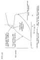
- FIG. 7is a graph showing the voltage-ampere characteristic in case of applying electrostatic pulses of ESD to the pad in the ESD protection apparatus of FIG. 1 ;
- FIG. 8is a graph showing the breakdown current values per unit length in case of using the ESD protection apparatus of FIG. 1 and in case of using a transverse parasitic bipolar transistor, a conventional MOS transistor;
- FIG. 9is a circuit diagram illustrating a second embodiment of an ESD protection apparatus of the present invention.
- FIG. 10is a plan view illustrating a third embodiment of an ESD protection apparatus of the present invention.
- FIG. 11is a longitudinal cross-section figure cut along the XI-XI line in FIG. 10 ;
- FIG. 12is a cross-section figure showing the method for fabricating the ESD protection apparatus of FIG. 10 and FIG. 11 ;
- FIG. 13is a cross-section figure showing the method for fabricating the ESD protection apparatus of FIG. 10 and FIG. 11 ;
- FIG. 14is a cross-section figure showing the method for fabricating the ESD protection apparatus of FIG. 10 and FIG. 11 ;
- FIG. 15is a cross-section figure showing the method for fabricating the ESD protection apparatus of FIG. 10 and FIG. 11 ;
- FIG. 16is a circuit diagram illustrating a fourth embodiment of an ESD protection apparatus of the present invention.
- FIG. 17is a plan view of the ESD protection apparatus in FIG. 16 ;
- FIG. 18is a longitudinal cross-section figure cut along the XVIII-XVIII line in FIG. 17 ;
- FIG. 19is a cross-section figure showing the method for fabricating the ESD protection apparatus of FIG. 16 ;
- FIG. 20is a cross-section figure showing the method for fabricating the ESD protection apparatus of FIG. 16 ;
- FIG. 21is a plan view illustrating a fifth embodiment of an ESD protection apparatus of the present invention.
- FIG. 22is a longitudinal cross-section figure cut along the XXII-XXII line in FIG. 21 ;
- FIG. 23is a plan view illustrating a sixth embodiment of an ESD protection apparatus of the present invention.
- FIG. 24is a longitudinal cross-section figure cut along the XXIV-XXIV line in FIG. 23 ;
- FIG. 25is a cross-section figure illustrating a seventh embodiment of an ESD protection apparatus of the present invention.
- FIG. 26is a circuit diagram showing a eighth embodiment of the ESD protection apparatus relevant to the present invention.
- FIG. 27is a longitudinal cross-sectional view of the ESD protection apparatus of FIG. 26 ;
- FIG. 28is a graph showing a comparison result of characteristics of a trigger element using the breakdown of an inverse diode and the trigger element multistage-connecting the forward diodes in series;
- FIG. 29is a graph showing an electric current voltage characteristic at the time when electrostatic pulses of the ESD are applied to the pad in the ESD protection apparatus of FIG. 26 ;
- FIG. 30is a circuit diagram showing a ninth embodiment of the ESD protection apparatus relevant to the present invention.
- FIG. 31is a cross-sectional view of a tenth embodiment of the ESD protection apparatus relevant to the present invention.
- FIG. 32Ais a cross-sectional view showing a diode comprising a P + layer/an N well formed in the existing CMOS process in the eighth embodiment;
- FIG. 32Bis a cross-sectional view showing one portion of the longitudinal bipolar transistor in the tenth embodiment.
- FIG. 33is a graph showing the voltage-ampere characteristic in case of applying electrostatic pulses of ESD of a pad in a conventional technique.
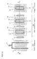
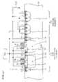
- FIG. 1 to FIG. 3illustrates a first embodiment of an ESD protection apparatus relevant to the present invention and FIG. 1 is a circuit diagram, FIG. 2 is a plan view, and FIG. 3 is a longitudinal cross-section figure along the III-III line in FIG. 2 .
- the ESD protection apparatus of this embodimentworks as an input buffer protection circuit.
- the ESD protection apparatus of this embodimentis installed between an input terminal (an input pad) 6 of a semiconductor integrated circuit chip and a CMOS transistor 100 and comprises a trigger element 310 comprising diodes 311 , 312 which are broken down by overvoltage applied to the input terminal 6 and an ESD protection element 210 comprising longitudinal bipolar transistors 211 , 212 for discharging the accumulated electric charge of the input terminal 6 by being electrically discharged owing to the breakdown of the diodes 311 , 312 .
- FIG. 2 and FIG. 3show only the longitudinal bipolar transistor 211 as some of ESD protection element 210 and only the diode 311 as some of the trigger element 310 .
- the CMOS transistor 100is a CMOS inverter comprising an NMOS transistor 101 and a PMOS transistor 102 .
- the cathodeis connected with the input terminal 6 and the anode is connected with the base of the longitudinal bipolar transistor 211 .
- the cathodeis connected with an electric power terminal 7 and the anode is connected with the base of the longitudinal bipolar transistor 212 .
- a resistor 313is connected with the anode of the diode 311 and a ground terminal 8 .
- a resistor 314is connected between the anode of the diode 312 and the input terminal 6 .
- the longitudinal bipolar transistors 211 , 212are both NPN type.
- the collectoris connected with the input terminal 6 and the emitter is connected with the ground terminal 8 .
- the collectoris connected with electric power terminal 7 and the emitter is connected with the input terminal 6 .
- the resistors 313 , 314are made of a singly crystal silicon, a polysilicon, a metal or the like formed in the same semiconductor integrated circuit chip.
- the ESD protection apparatus 210Since today it has swiftly been promoted to make the gate insulation film of a CMOS transistor thinner, it is required for the ESD protection apparatus 210 to work at a lower voltage than that which the gate insulation film of the CMOS transistor 100 is broken.
- the base potential of the longitudinal bipolar transistors 211 , 212is increased by voltage decreased at the time when the trigger current, which is the breakdown current of the diodes 311 , 312 , flows in the resistors 313 , 314 to turn on longitudinal bipolar transistors 211 , 212 . Consequently, the large quantity of the electric charge attributed to the static electricity accumulated in the input terminal 6 is released in the longitudinal direction of the silicon substrate. As a result, electric current concentration can be prevented and a high ESD withstand level can be obtained.
- the trigger element 310comprising the ESD protection element 210 comprising longitudinal bipolar transistors 211 , 212 and the diodes 311 , 312 can be carried out by adding only one ion implantation mask in the common fabrication process of a CMOSFET.
- the fabrication methodwill be described with the reference to FIG. 2 and FIG. 3 .
- the ESD protection element 210will be described. Simultaneously with the N + type diffusion layer 1 of the CMOS transistor 100 , the collector lead parts 10 and the emitters 11 are formed and simultaneously with the P + type diffusion layer 2 of the CMOS transistor 100 , the base lead parts 12 are formed.
- the dummy gate electrodes 13 formed simultaneously with the gate electrodes 3 of the CMOS transistor 100are employed in order to separate the silicide of the emitters 11 and the base lead parts 12 .
- the dummy gate electrodes 13are not for applying potential but separate the silicide. Opening parts 50 are formed in a resist using an additional mask for ion implantation and ion implantation is carried out to simultaneously form the P ⁇ region bases 16 and the collector N wells 17 .
- the collector N wells 17 formed at that time and the collector lead parts 10 formed separatelyare connected with each other by the N wells 14 for connection simultaneously formed with the N well 5 of the CMOS transistor 100 . Consequently, longitudinal bipolar transistors can be fabricated utilizing the CMOS process. Incidentally, the ion implantation may be carried out either before or after of the formation of the gate electrodes 3 .
- the trigger element 310will be described next.
- the N + P ⁇ type diodehas the same structure as the emitters 11 and bases 16 of the ESD protection element 210 and simultaneously with the N + type diffusion layer 1 of the CMOS transistor 100 , the N + part 21 is formed and simultaneously with the P + type diffusion layer 2 of the CMOS transistor 100 , the lead parts 22 of the P ⁇ parts 26 are formed. Consequently, it is enabled to set a desired trigger voltage and the leakage level in the opposed direction.
- FIG. 4 to FIG. 6are cross-section illustrations illustrating the method for fabricating the ESD protection apparatus of this embodiment.
- the method for fabricating the ESD protection apparatus of the present inventionwill be described in details.
- collector lead parts 10 and N wells 14 for connection of the ESD protection element 210are formed.
- the doping concentration of these regionsis about 10 17 /cm ⁇ 3 to 10 18 /cm ⁇ 3 .
- the dummy gate electrodes 13 of the ESD protection element 210 and a dummy gate electrode 23 of the trigger element 310are formed. That is for preventing the emitters 11 and the base lead parts 12 of the ESD protection element 210 from being connected with the silicide formed later on the diffusion layer. In the same manner, that is for preventing the N + part 21 and the lead parts 22 of trigger element 310 from being connected with the silicide later.
- ion implantation in about 10 18 /cm ⁇ 3 doseis carried out to form the bases 16 of the ESD protection element 210 and continuously ion implantation in about 10 18 /cm ⁇ 3 dose is carried out to form the collector N wells 17 .
- the P ⁇ part 26 and the N well 27 of the trigger element 310are simultaneously formed.
- the following descriptionis of the operation at the time when the electrostatic pulses are applied to the input terminal 6 .
- high voltageis applied to the ESD protection element 210 , trigger element 310 , and the gate insulation film of the CMOS transistors 100 . Therefore, it is required to release the electric charge by ESD by operation of the ESD protection element 210 before the gate insulation film of the CMOS transistors 100 is broken down.
- the gate insulation film of the CMOS transistors 100is 4 nm, the gate insulation film is broken by stress of constant voltage of about 8V. That is, it is required for the ESD protection element 210 to operate at a voltage lower than that.
- the ESD protection element 210which comprises longitudinal bipolar transistors, is formed, since the withstand voltage between the collector N wells 17 and the P ⁇ region bases 16 are about as high as 10V, it is insufficient to protect the CMOS transistors 100 whose gate insulation film is thin and fine only by the ESD protection element 210 .
- the trigger element 310which operates at a voltage as low as possible and not lower than the electric power source voltage. Since the P ⁇ part 26 of the trigger element 310 is formed by ion implantation, a desired trigger voltage or leakage level in the opposed direction can be set by controlling the dose quantity and it is easy to obtain trigger voltage of about 4 V.
- FIG. 7shows the voltage-ampere characteristic in case of electrostatic pulses application to the pad.
- the trigger element 310works at about 4 V
- the resultant trigger current and the resistor 313increase the base potential of the ESD protection element 210 to start the ESD protection element 210 .
- the electric charge applied to the input terminal 6 by the ESDcan be released to the ground terminal 8 through the longitudinal bipolar transistor 211 . Consequently, if the withstand voltage of the gate insulation film of the inner circuits of the CMOS transistors 100 is 8 V, the electric charge can be released at a lower voltage than that, so that the breakdown of the gate insulation film can be prevented.
- FIG. 8shows the breakdown electric current values per unit length in case of using the ESD protection apparatus of the present invention and in case of using a transverse parasitic bipolar transistor, which is a conventional MOS transistor.
- the breakdown electric current of the ESD protection element of this embodiment comprising longitudinal bipolar transistorsis higher than that of an ESD protection element comprising transverse bipolar transistors.
- the inner gate insulation filmis as thin as about 2 nm, the breakdown electric current is sharply lowered in case of the transverse bipolar transistors, the decrease is slight in case of the longitudinal bipolar transistors.
- FIG. 9is a circuit diagram showing a second embodiment of an ESD protection apparatus relevant to the present invention. Hereinafter, description will be given with reference to the figure.
- the ESD protection apparatus of this embodimentworks as an electric power source protection circuit.
- the ESD protection apparatus of this embodimentis installed between an electric power terminal (an electric power pad) 7 of a semiconductor integrated circuit chip and an inner circuit 103 and comprises a trigger element 315 comprising a diode 316 to be broken down by overvoltage applied to the electric power terminal 7 and an ESD protection element 213 comprising a longitudinal bipolar transistor 214 for discharging the accumulated electric charge of the electric power terminal 7 by being electrically discharged owing to the breakdown of the diode 316 .
- the cathodeis connected with the electric power terminal 7 and the anode is connected with the base of the longitudinal bipolar transistor 214 .
- a resistor 317is connected between the anode of the diode 316 and a ground terminal 8 .
- the longitudinal bipolar transistor 214it is NPN type, and the collector is connected with the electric power terminal 7 and the emitter is connected with the ground terminal 8 .
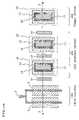
- FIG. 10 to FIG. 15illustrate a third embodiment of an ESD protection apparatus relevant to the present invention.
- FIG. 10shows a plan view
- FIG. 11shows the longitudinal cross-section figure cut along the XI-XI line in FIG. 10
- FIG. 12 to FIG. 15show the cross-section figures illustrating the fabrication method.
- descriptionwill be given with reference to these figures. Incidentally, the same reference numerals are assigned to these same as the parts in FIG. 2 and FIG. 6 and their description is omitted.
- the ESD protection apparatus of this embodimentis an example in which insulation films 18 , 28 (SiO 2 or SiN) covering the diffusion layer as to prevent silicide formation are used for resistor element formation in place of the dummy gate electrodes 13 , 23 for silicide separation (in FIG. 2 and FIG. 3 ).
- the N well 14 for connection with the collector lead parts 10 of the ESD protection element 200is formed.
- ion implantationis carried out to form the bases 16 of the ESD protection element 200 and continuously ion implantation is carried out to form the collector N wells 17 .
- the P ⁇ part 26 and the N well 27 of the trigger element 300are simultaneously formed.
- the insulation film 18 in ESD protection element 200 and the insulation film 28 in the trigger element 310are formed. That is for preventing the connection of the emitters 11 and the base lead parts 12 of ESD protection element 200 with each other by the silicide formed in the diffusion layer thereafter. Simultaneously, that is also for preventing the connection of the N + part 21 and the lead parts 22 of trigger element 300 with each other by the silicide.
- wiringsare formed on these upper layers to form a circuit as illustrated in FIG. 1 .
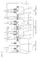
- FIG. 16 to FIG. 18illustrate a fourth embodiment of an ESD protection apparatus relevant to the present invention.
- FIG. 16shows a circuit diagram
- FIG. 17shows a plan view
- FIG. 18shows the longitudinal cross-section figure cut along the XVIII-XVIII line in FIG. 17 .
- the trigger elementis also used as a longitudinal bipolar transistor of the ESD protection element.
- the ESD protection apparatus of this embodimentis installed between an, electric power terminal (an electric power pad) 7 of a semiconductor integrated circuit chip and an inner circuit 103 and comprises a trigger element 400 comprising a diode 402 to be broken down by overvoltage applied to the electric power terminal 7 and an ESD protection element 200 comprising a longitudinal bipolar transistor 201 for discharging the accumulated electric charge of the electric power terminal 7 by being electrically discharged owing to the breakdown of the diode 402 .
- the diode 402is between the collector and the base of the longitudinal bipolar transistor 401 .
- the cathode of the diode 402which the collector of the longitudinal bipolar transistor 401 , is connected with the electric power terminal 7 and the anode of the diode 402 , which is the base of the longitudinal bipolar transistor 401 , is connected with the base of the longitudinal bipolar transistor 201 .
- a resistor 403is connected between the anode of the diode 402 , which is the base of the longitudinal bipolar transistor 401 , and a ground terminal 8 .
- the longitudinal bipolar transistors 201 , 402they are NPN type, and the collector is connected with the electric power terminal 7 and the emitter is connected with the ground terminal 8 .
- emitter lead parts 40are formed in the trigger element 400 and connected as illustrated in FIG. 16 and FIG. 18 .
- the longitudinal bipolar transistor 401is formed in the trigger element 400 and the trigger element 400 can work as an ESD protection element.
- the base potential of the longitudinal bipolar transistors 201 , 401is increased by the trigger current of the diode 402 composed of the N + part (the collector) 41 and the P ⁇ part (the base) 46 of the trigger element 400 and the resistor 403 and owing the cooperation, the electric charge attributed to the static electricity accumulated in the electric power terminal 7 can be released by both of them.
- the ESD protection apparatus of this embodimentis employed as the electric power pad, it may be also employed as an input pad or an output pad by installing two as same in the first embodiment.
- FIG. 19 and FIG. 20are cross-section figures illustrating the method for fabricating the ESD protection apparatus of this embodiment.
- FIG. 19 and FIG. 20are cross-section figures illustrating the method for fabricating the ESD protection apparatus of this embodiment.
- detailed description of the method for fabricating the ESD protection apparatus of this embodimentwill be given with reference to FIG. 18 to FIG. 20 .
- N wells 14 for connection for the collector lead parts 10 of the ESD protection element 200 and N wells 44 for emitter connection of the trigger element 400are formed.
- ion implantationis carried out to form the bases 16 of the ESD protection element 200 and continuously ion implantation is, carried out to form the collector N wells 17 .
- the P ⁇ part 46 and the emitter N well 47 of the trigger element 400are simultaneously formed.
- the collector lead parts 10 and emitters 11 of the ESD protection element 200are formed.
- the emitter lead parts 40 and collector 41 of the trigger element 400are formed.
- the base lead parts 12 and lead parts 42 of the P ⁇ parts 46 to be base of the trigger element 400are formed.
- the insulation film 18 of the ESD protection element 200 and the insulation film 48 of the trigger element 400are formed. That is for preventing the emitters 11 and the base lead parts 12 of the ESD protection element 200 from being connected with the silicide formed later on the diffusion layer. In the same manner, that is for preventing the N + part 41 and the lead parts 42 of trigger element 400 from being connected with the silicide later.
- wiringsare formed on these upper layers to form a circuit as illustrated in FIG. 16 .
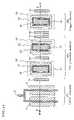
- FIG. 21 to FIG. 22illustrate a fifth embodiment of an ESD protection apparatus relevant to the present invention.
- FIG. 21shows a plan view
- FIG. 22shows the longitudinal cross-section figure cut along the XXII-XXII line in FIG. 21 .
- the collector of the ESD protection elementsis utilized in common in order to miniaturize the surface area.
- the ESD protection apparatus 230 of this embodimentcomprises one collector N well 17 ′ by making two collector N wells 17 in common in the ESD protection element 200 of the third embodiment illustrated in FIG. 10 and FIG. 11 .
- the surface areais miniaturized by using collector lead parts 10 only in both ends of the collector N well 17 ′.
- the method for fabricating the ESD protection apparatus of this embodimentis same as that of the third embodiment illustrated in FIG. 12 to FIG. 15 .
- FIG. 23 to FIG. 24illustrate a sixth embodiment of an ESD protection apparatus relevant to the present invention.
- FIG. 23shows a plan view and
- FIG. 24shows the longitudinal cross-section figure cut along the XXIV-XXIV line in FIG. 23 .
- the ESD protection element and the trigger elementare made in common in order to miniaturize the surface area.
- the ESD protection elements 240 and the trigger element 310 of this embodimentare formed by combining two bases 16 and the P ⁇ part 26 of the ESD protection element 200 and the trigger element 300 in the third embodiment illustrated in FIG. 10 and FIG. 11 into one base 16 ′ and at the same time combining two collector N wells 17 and the N well 27 of the ESD protection element 200 and the trigger element 300 in the third embodiment into one collector N well 19 .
- the surface areais miniaturized by using collector lead parts 10 of the ESD protection elements 240 only in both ends.
- the method for fabricating the ESD protection apparatus of this embodimentis same as that of the third embodiment illustrated in FIG. 12 to FIG. 15 .
- FIG. 25illustrates the longitudinal cross-section figure of a seventh embodiment of an ESD protection apparatus relevant to the present invention.
- the ESD protection elementis made to be a trigger element capable of triggering at lower voltage.
- the ESD protection apparatus of this embodimentis same as the first embodiment except that the dummy gate electrode 23 of the trigger element 310 is fixed in the ground. In case of fixing the dummy gate electrodes 23 of the trigger element 310 in the ground, the electric field is intensified between the N + part 21 and the dummy gate electrodes 23 , so that triggering is caused at a lower voltage.
- FIG. 26 and FIG. 27show a eighth embodiment of the ESD protection apparatus relevant to the present invention
- FIG. 26is a circuit diagram
- FIG. 27is a cross-sectional view.
- the ESD protection apparatus of the present embodimentacts as an input buffer protection circuit.
- the ESD protection apparatus of the present embodimentis installed between an input terminal (an input pad) 6 of a semiconductor integrated circuit chip and a CMOS transistor 100 and comprises a trigger element 510 comprising diodes 511 , 512 which are broken down by overvoltage applied to the input terminal 6 and an ESD protection element 210 comprising longitudinal bipolar transistors 211 , 212 for discharging the accumulated electric charge of the input terminal 6 by being electrically discharged owing to the breakdown of the diodes 511 , 512 .
- the diodes 511 , 512are a plurality of diodes connected in series, and the overvoltage is a forward voltage for the diodes 511 , 512 and the breakdown is a substantial breakdown by being electrically discharged.
- the diodes 511 , 512are illustrated in FIG. 26 as four diodes connected in series, but in FIG. 27 simplified and illustrated as two diodes connected in series for convenience's sake.
- a cathodeis connected with a base of the longitudinal bipolar transistor 211 and an anode is connected with the input terminal 6 .
- the cathodeis connected with the base of the longitudinal bipolar transistor 212 and the anode is connected with an electric power source terminal 7 .
- a resistor 313is connected between the cathode of the diode 511 and a ground terminal 8 .
- a resistor 314is connected between the cathode of the diode 512 and the input terminal 6 .
- the longitudinal bipolar transistor 211 , 212use the same transistors as those of a first embodiment.
- the diodes 511 , 512are formed by an N+ diffusion layer 1 , a P+ diffusion layer 2 and an N well 5 and the like which are formed at the time of the usual CMOS process.
- the breakdown of the inverse diodewas utilized.
- the trigger element 510 multistage-connected for raising a forward diode equal to or more than an electric power source voltageis employed.
- a low voltage operation device having equal to or less than 1.5Vhas an extremely thin gate insulation film and therefore is broken down by application of equal to or more than 5V.
- the present embodimentis effective.
- serial connection stages of the diode corresponding to the electric power source voltagea desired trigger voltage can be secured.
- FIG. 28is a graph showing a comparison result of the characteristics of the trigger element utilizing the breakdown of the inverse diode and the trigger element multistage-connecting the forward diodes in series.
- FIG. 29is a graph showing an electric current voltage characteristic when an ESD electrostatic pulse is applied to a pad in the ESD protection apparatus of the present embodiment.
- descriptionwill be given with reference to this illustration.
- the CMOS device operating at a low voltage of about 1.2Vuses an extremely thin gate insulation film having a thickness of about equal to or less than 2.5 nm.
- the breakdown withstand pressure of this gate insulation filmis about 4V to 5V.
- FIG. 30is a circuit diagram showing a ninth embodiment of the ESD protection apparatus relevant to the present invention. Hereinafter, description will be given with reference to this illustration.
- the ESD protection apparatus of the present embodimentacts as an electric power source protection circuit.
- the ESD protection apparatus of the present embodimentcomprises a trigger element 515 comprising a diode 516 which is provided between the power source terminal 7 and the inner circuit 103 of the semiconductor integrated circuit and is broken down by overvoltage applied to an electric power source terminal 7 , and an ESD protection element 213 comprising the longitudinal bipolar transistor 214 for discharging the accumulated electric charge of the electric power source terminal 7 by being electrically discharged owing to the breakdown of the diode 516 .
- the diode 516is a plurality of diodes connected in series, and the overvoltage is a forward voltage for the diode 516 and the breakdown is a substantial breakdown by being electrically discharged.
- a cathodeis connected with a base of the longitudinal bipolar transistor 214 and an anode is connected with the electric power source terminal 7 .
- a resistor 317is connected between the cathode of the diode 516 and a ground terminal 8 .
- a longitudinal bipolar transistor 214is of NPN type, and its collector is connected with the electric power source terminal 7 , and its emitter is connected with the ground terminal 8 .
- FIG. 27A cross-sectional view thereof corresponds to FIG. 27 . Consequently, the ESD protection apparatus of the present embodiment also performs the same functions and effects as the eighth embodiment.
- FIG. 31is a cross-sectional view showing a tenth embodiment of the ESD protection apparatus relevant to the present invention.
- descriptionwill be given with reference to the illustration.
- the circuit diagram of the ESD protection apparatus of the present embodimentis the same as the eighth embodiment ( FIG. 26 ).
- the diodes simultaneously formed at the time when the longitudinal bipolar transistor is formedare used by connecting them in series in a forward direction.
- a diode comprising P + layers 2 /an N well 5is used.
- a diode comprising an N + layer 521 /a P ⁇ layer 526 formed at the time when the longitudinal bipolar transistor is formedis used.
- a resistance of a wellis dominant and this resistance determines a discharging capacity.
- the electric currentflows under a separation region and therefore a resistance is increased.
- a separation between the P + layer 522 /the N + layer 521is performed by a dummy gate 523 at a formation time of the longitudinal bipolar transistor, and since adjustment of the concentration of the P ⁇ layer 526 is possible by additional injection of the longitudinal bipolar transistor, the lowering of the resistance at the high electric current area is possible.
- the diode comprising the P + layers 2 /the N well 5 as shown in FIG. 27since a parasitic longitudinal bipolar transistor comprising the P + 2 layer/the N well 5 /a P substrate 51 is formed, the electric current flowing into the P substrate 51 is generated. For this reason, the electric current to be supplied to the longitudinal bipolar transistor which is a protection element is reduced.
- the diode comprising the N + layer 521 /the P ⁇ layer 526can prevent the electric current flowing in a longitudinal direction (depth direction of substrate), and therefore the electric current can be supplied to the base of the ESD protection element 210 with high efficiency (refer to FIG. 32 ). Consequently, according to the present embodiment, since a trigger electric current can be supplied to a base of the longitudinal bipolar transistor with high efficiency, the size of the trigger element can be reduced.
- the present inventionis, needless to mention, not limited to the foregoing first to the tenth embodiments.
- the P typemay be taken as the N type and the N type may be taken as the P type. Consequently, the NPN type may be taken as the PNP type with each N type and P type taken as the inverse conductive type.
- an ESD protection apparatus of the present inventionsince the breakdown voltage of a diode is used as a trigger of a longitudinal bipolar transistor, electric current concentration and electric field concentration are hardly caused in junction parts even if miniaturization is promoted and moreover the characteristic of triggering at a low voltage can be obtained.
- the method for fabricating an ESD protection apparatus of the present inventionis make it easy to fabricate an ESD protection apparatus of the present invention by adding only one mask in a common CMOS process.
- the effects of the present inventionis as follows.
- the first effectis that since electric current is released in the longitudinal direction by employing a longitudinal bipolar transistor, electric current concentration is suppressed as compared with the case of releasing the electric current in the transverse direction by using a conventional CMOSFET type parasitic bipolar transistor and consequently the ESD protection element itself is hardly broken.
- the second effectis that since the electric current to be discharged for the same surface area is high, the surface area required for an ESD protection element can be miniaturized and consequently decrease of the input capacity necessary for high speed operation can be performed.
- the third effectis that since a longitudinal bipolar transistor and a trigger element can be formed by adding only one ion implantation mask for an ESD protection circuit in a common CMOSFET process, the fabrication method is carried out in a compatible process with the CMOSFET process.
- the fourth effectis that owing to the trigger element capable of working a low voltage, the breakdown of the gate insulation film in CMOSFET can be prevented.
- the fifth effectis that an element capable of triggering at a desired voltage can be form.
Landscapes
- Semiconductor Integrated Circuits (AREA)
- Metal-Oxide And Bipolar Metal-Oxide Semiconductor Integrated Circuits (AREA)
Abstract
Description
Claims (6)
Priority Applications (2)
| Application Number | Priority Date | Filing Date | Title |
|---|---|---|---|
| US11/442,288US7294542B2 (en) | 2000-05-15 | 2006-05-30 | Method of fabricating a semiconductor device having CMOS transistors and a bipolar transistor |
| US11/649,211US7629210B2 (en) | 2000-05-15 | 2007-01-04 | Method for fabricating an ESD protection apparatus for discharging electric charge in a depth direction |
Applications Claiming Priority (4)
| Application Number | Priority Date | Filing Date | Title |
|---|---|---|---|
| JP2000141304 | 2000-05-15 | ||
| JP2000-141304 | 2000-05-15 | ||
| US09/852,735US20010043449A1 (en) | 2000-05-15 | 2001-05-11 | ESD protection apparatus and method for fabricating the same |
| US11/442,288US7294542B2 (en) | 2000-05-15 | 2006-05-30 | Method of fabricating a semiconductor device having CMOS transistors and a bipolar transistor |
Related Parent Applications (2)
| Application Number | Title | Priority Date | Filing Date |
|---|---|---|---|
| US09/852,735DivisionUS20010043449A1 (en) | 2000-05-15 | 2001-05-11 | ESD protection apparatus and method for fabricating the same |
| US09/852,735ContinuationUS20010043449A1 (en) | 2000-05-15 | 2001-05-11 | ESD protection apparatus and method for fabricating the same |
Related Child Applications (1)
| Application Number | Title | Priority Date | Filing Date |
|---|---|---|---|
| US11/649,211Continuation-In-PartUS7629210B2 (en) | 2000-05-15 | 2007-01-04 | Method for fabricating an ESD protection apparatus for discharging electric charge in a depth direction |
Publications (2)
| Publication Number | Publication Date |
|---|---|
| US20060223258A1 US20060223258A1 (en) | 2006-10-05 |
| US7294542B2true US7294542B2 (en) | 2007-11-13 |
Family
ID=18648438
Family Applications (2)
| Application Number | Title | Priority Date | Filing Date |
|---|---|---|---|
| US09/852,735AbandonedUS20010043449A1 (en) | 2000-05-15 | 2001-05-11 | ESD protection apparatus and method for fabricating the same |
| US11/442,288Expired - Fee RelatedUS7294542B2 (en) | 2000-05-15 | 2006-05-30 | Method of fabricating a semiconductor device having CMOS transistors and a bipolar transistor |
Family Applications Before (1)
| Application Number | Title | Priority Date | Filing Date |
|---|---|---|---|
| US09/852,735AbandonedUS20010043449A1 (en) | 2000-05-15 | 2001-05-11 | ESD protection apparatus and method for fabricating the same |
Country Status (3)
| Country | Link |
|---|---|
| US (2) | US20010043449A1 (en) |
| KR (1) | KR100433691B1 (en) |
| TW (1) | TW480701B (en) |
Cited By (50)
| Publication number | Priority date | Publication date | Assignee | Title |
|---|---|---|---|---|
| US20070194380A1 (en)* | 2000-05-15 | 2007-08-23 | Mototsugu Okushima | Method for fabricating an ESD protection apparatus for discharging electric charge in a depth direction |
| US20080203435A1 (en)* | 2007-02-27 | 2008-08-28 | Nec Electronics Corporation | Semiconductor device having elongated electrostatic protection element along long side of semiconductor chip |
| US20090089719A1 (en)* | 2007-10-02 | 2009-04-02 | International Business Machines Corporation | Structure for a Stacked Power Clamp Having a BigFET Gate Pull-Up Circuit |
| US20100214704A1 (en)* | 2009-02-26 | 2010-08-26 | Freescale Semiconductor, Inc. | Esd protection using isolated diodes |
| US20120044736A1 (en)* | 2010-08-20 | 2012-02-23 | Chung Shine C | Memory devices using a plurality of diodes as program selectors for memory cells |
| US8804398B2 (en) | 2010-08-20 | 2014-08-12 | Shine C. Chung | Reversible resistive memory using diodes formed in CMOS processes as program selectors |
| US8830720B2 (en) | 2010-08-20 | 2014-09-09 | Shine C. Chung | Circuit and system of using junction diode as program selector and MOS as read selector for one-time programmable devices |
| US8848423B2 (en) | 2011-02-14 | 2014-09-30 | Shine C. Chung | Circuit and system of using FinFET for building programmable resistive devices |
| US8861249B2 (en) | 2012-02-06 | 2014-10-14 | Shine C. Chung | Circuit and system of a low density one-time programmable memory |
| US8913415B2 (en) | 2010-08-20 | 2014-12-16 | Shine C. Chung | Circuit and system for using junction diode as program selector for one-time programmable devices |
| US8913449B2 (en) | 2012-03-11 | 2014-12-16 | Shine C. Chung | System and method of in-system repairs or configurations for memories |
| US8912576B2 (en) | 2011-11-15 | 2014-12-16 | Shine C. Chung | Structures and techniques for using semiconductor body to construct bipolar junction transistors |
| US8917533B2 (en) | 2012-02-06 | 2014-12-23 | Shine C. Chung | Circuit and system for testing a one-time programmable (OTP) memory |
| US8923085B2 (en) | 2010-11-03 | 2014-12-30 | Shine C. Chung | Low-pin-count non-volatile memory embedded in a integrated circuit without any additional pins for access |
| US8988965B2 (en) | 2010-11-03 | 2015-03-24 | Shine C. Chung | Low-pin-count non-volatile memory interface |
| US9007804B2 (en) | 2012-02-06 | 2015-04-14 | Shine C. Chung | Circuit and system of protective mechanisms for programmable resistive memories |
| US9019791B2 (en) | 2010-11-03 | 2015-04-28 | Shine C. Chung | Low-pin-count non-volatile memory interface for 3D IC |
| US9019742B2 (en) | 2010-08-20 | 2015-04-28 | Shine C. Chung | Multiple-state one-time programmable (OTP) memory to function as multi-time programmable (MTP) memory |
| US9025357B2 (en) | 2010-08-20 | 2015-05-05 | Shine C. Chung | Programmable resistive memory unit with data and reference cells |
| US9042153B2 (en) | 2010-08-20 | 2015-05-26 | Shine C. Chung | Programmable resistive memory unit with multiple cells to improve yield and reliability |
| US9070437B2 (en) | 2010-08-20 | 2015-06-30 | Shine C. Chung | Circuit and system of using junction diode as program selector for one-time programmable devices with heat sink |
| US9076526B2 (en) | 2012-09-10 | 2015-07-07 | Shine C. Chung | OTP memories functioning as an MTP memory |
| US9136261B2 (en) | 2011-11-15 | 2015-09-15 | Shine C. Chung | Structures and techniques for using mesh-structure diodes for electro-static discharge (ESD) protection |
| US9183897B2 (en) | 2012-09-30 | 2015-11-10 | Shine C. Chung | Circuits and methods of a self-timed high speed SRAM |
| US9224496B2 (en) | 2010-08-11 | 2015-12-29 | Shine C. Chung | Circuit and system of aggregated area anti-fuse in CMOS processes |
| US9236141B2 (en) | 2010-08-20 | 2016-01-12 | Shine C. Chung | Circuit and system of using junction diode of MOS as program selector for programmable resistive devices |
| US9251893B2 (en) | 2010-08-20 | 2016-02-02 | Shine C. Chung | Multiple-bit programmable resistive memory using diode as program selector |
| US9324447B2 (en) | 2012-11-20 | 2016-04-26 | Shine C. Chung | Circuit and system for concurrently programming multiple bits of OTP memory devices |
| US9324849B2 (en) | 2011-11-15 | 2016-04-26 | Shine C. Chung | Structures and techniques for using semiconductor body to construct SCR, DIAC, or TRIAC |
| US9412473B2 (en) | 2014-06-16 | 2016-08-09 | Shine C. Chung | System and method of a novel redundancy scheme for OTP |
| US9431127B2 (en) | 2010-08-20 | 2016-08-30 | Shine C. Chung | Circuit and system of using junction diode as program selector for metal fuses for one-time programmable devices |
| US9460807B2 (en) | 2010-08-20 | 2016-10-04 | Shine C. Chung | One-time programmable memory devices using FinFET technology |
| US9478534B2 (en) | 2013-10-08 | 2016-10-25 | Globalfoundries Inc. | Lateral BiCMOS replacement metal gate |
| US9496033B2 (en) | 2010-08-20 | 2016-11-15 | Attopsemi Technology Co., Ltd | Method and system of programmable resistive devices with read capability using a low supply voltage |
| US9496265B2 (en) | 2010-12-08 | 2016-11-15 | Attopsemi Technology Co., Ltd | Circuit and system of a high density anti-fuse |
| US9711237B2 (en) | 2010-08-20 | 2017-07-18 | Attopsemi Technology Co., Ltd. | Method and structure for reliable electrical fuse programming |
| US9818478B2 (en) | 2012-12-07 | 2017-11-14 | Attopsemi Technology Co., Ltd | Programmable resistive device and memory using diode as selector |
| US9824768B2 (en) | 2015-03-22 | 2017-11-21 | Attopsemi Technology Co., Ltd | Integrated OTP memory for providing MTP memory |
| US10192615B2 (en) | 2011-02-14 | 2019-01-29 | Attopsemi Technology Co., Ltd | One-time programmable devices having a semiconductor fin structure with a divided active region |
| US10229746B2 (en) | 2010-08-20 | 2019-03-12 | Attopsemi Technology Co., Ltd | OTP memory with high data security |
| US10249379B2 (en) | 2010-08-20 | 2019-04-02 | Attopsemi Technology Co., Ltd | One-time programmable devices having program selector for electrical fuses with extended area |
| US10535413B2 (en) | 2017-04-14 | 2020-01-14 | Attopsemi Technology Co., Ltd | Low power read operation for programmable resistive memories |
| US10586832B2 (en) | 2011-02-14 | 2020-03-10 | Attopsemi Technology Co., Ltd | One-time programmable devices using gate-all-around structures |
| US10726914B2 (en) | 2017-04-14 | 2020-07-28 | Attopsemi Technology Co. Ltd | Programmable resistive memories with low power read operation and novel sensing scheme |
| US10770160B2 (en) | 2017-11-30 | 2020-09-08 | Attopsemi Technology Co., Ltd | Programmable resistive memory formed by bit slices from a standard cell library |
| US10916317B2 (en) | 2010-08-20 | 2021-02-09 | Attopsemi Technology Co., Ltd | Programmable resistance memory on thin film transistor technology |
| US10923204B2 (en) | 2010-08-20 | 2021-02-16 | Attopsemi Technology Co., Ltd | Fully testible OTP memory |
| US11062786B2 (en) | 2017-04-14 | 2021-07-13 | Attopsemi Technology Co., Ltd | One-time programmable memories with low power read operation and novel sensing scheme |
| US20220131459A1 (en)* | 2020-10-26 | 2022-04-28 | Commissariat A L'energie Atomique Et Aux Energies Alternatives | Assembly of semiconductor power modules |
| US11615859B2 (en) | 2017-04-14 | 2023-03-28 | Attopsemi Technology Co., Ltd | One-time programmable memories with ultra-low power read operation and novel sensing scheme |
Families Citing this family (44)
| Publication number | Priority date | Publication date | Assignee | Title |
|---|---|---|---|---|
| TW529150B (en)* | 2002-02-06 | 2003-04-21 | Ind Tech Res Inst | Integrated circuit device used in electrostatic discharge (ESD) protection and the ESD protection circuit using the same |
| US7638847B1 (en)* | 2002-11-14 | 2009-12-29 | Altera Corporation | ESD protection structure |
| USRE43922E1 (en)* | 2003-06-13 | 2013-01-15 | National Semiconductor Corporation | Balanced cells with fabrication mismatches that produce a unique number generator |
| US7482657B1 (en) | 2003-06-13 | 2009-01-27 | National Semiconductor Corporation | Balanced cells with fabrication mismatches that produce a unique number generator |
| TW594969B (en)* | 2003-07-02 | 2004-06-21 | Realtek Semiconductor Corp | ESD clamp circuit |
| TWI266406B (en) | 2003-10-14 | 2006-11-11 | Realtek Semiconductor Corp | Electrostatic discharge protection circuit for a voltage source |
| KR20060086178A (en) | 2005-01-26 | 2006-07-31 | 삼성전자주식회사 | Liquid crystal display |
| KR101159114B1 (en)* | 2005-05-25 | 2012-06-25 | 매그나칩 반도체 유한회사 | ESD Protection Device |
| CN100536132C (en)* | 2005-06-20 | 2009-09-02 | 昂宝电子(上海)有限公司 | ESD protection system and method for multi voltage signal |
| JP5108250B2 (en)* | 2006-04-24 | 2012-12-26 | オンセミコンダクター・トレーディング・リミテッド | Semiconductor device and manufacturing method thereof |
| JP2007294613A (en)* | 2006-04-24 | 2007-11-08 | Sanyo Electric Co Ltd | Semiconductor device and manufacturing method thereof |
| US7875513B2 (en)* | 2006-04-26 | 2011-01-25 | Fabio Pellizzer | Self-aligned bipolar junction transistors |
| JP2007317869A (en)* | 2006-05-25 | 2007-12-06 | Sanyo Electric Co Ltd | Semiconductor device and manufacturing method thereof |
| US20070297105A1 (en)* | 2006-06-23 | 2007-12-27 | Brennan Ciaran J | Active ESD Protection |
| US20070297106A1 (en)* | 2006-06-23 | 2007-12-27 | Dai Peter H | Esd and electric surge protected circuit and method of making same |
| US7910441B2 (en)* | 2006-07-19 | 2011-03-22 | Freescale Semiconductor, Inc. | Multi-gate semiconductor device and method for forming the same |
| JP5041760B2 (en)* | 2006-08-08 | 2012-10-03 | ルネサスエレクトロニクス株式会社 | Semiconductor integrated circuit device |
| JP5045027B2 (en)* | 2006-08-15 | 2012-10-10 | 富士通セミコンダクター株式会社 | Electrostatic discharge protection circuit and semiconductor device |
| US7795102B1 (en)* | 2007-01-17 | 2010-09-14 | National Semiconductor Corporation | ESD high frequency diodes |
| JP5252830B2 (en)* | 2007-05-10 | 2013-07-31 | セミコンダクター・コンポーネンツ・インダストリーズ・リミテッド・ライアビリティ・カンパニー | Semiconductor integrated circuit |
| US7701682B2 (en)* | 2008-01-31 | 2010-04-20 | Freescale Semiconductors, Inc. | Electrostatic discharge protection |
| US7911750B2 (en)* | 2008-02-27 | 2011-03-22 | Freescale Semiconductor, Inc. | Resistor triggered electrostatic discharge protection |
| US8237227B2 (en)* | 2008-08-29 | 2012-08-07 | Taiwan Semiconductor Manufacturing Company, Ltd. | Dummy gate structure for gate last process |
| US20100301389A1 (en)* | 2009-05-29 | 2010-12-02 | Kushner Vadim A | Esd protection structure |
| US8193560B2 (en) | 2009-06-18 | 2012-06-05 | Freescale Semiconductor, Inc. | Voltage limiting devices |
| DE102009039247B9 (en) | 2009-08-28 | 2012-01-26 | Austriamicrosystems Ag | Semiconductor body with a connection cell |
| DE102009061167B3 (en)* | 2009-08-28 | 2015-03-05 | Austriamicrosystems Ag | Semiconductor body with a connection cell |
| JP5441724B2 (en)* | 2010-01-08 | 2014-03-12 | パナソニック株式会社 | ESD protection element, semiconductor device and plasma display device |
| US20120153347A1 (en)* | 2010-12-17 | 2012-06-21 | National Semiconductor Corporation | ESD clamp with auto biasing under high injection conditions |
| US8482078B2 (en) | 2011-05-10 | 2013-07-09 | International Business Machines Corporation | Integrated circuit diode |
| US8710627B2 (en)* | 2011-06-28 | 2014-04-29 | Alpha And Omega Semiconductor Incorporated | Uni-directional transient voltage suppressor (TVS) |
| US8304838B1 (en) | 2011-08-23 | 2012-11-06 | Amazing Microelectronics Corp. | Electrostatic discharge protection device structure |
| US8982518B2 (en)* | 2013-03-14 | 2015-03-17 | The Boeing Company | Methods and apparatus to provide transient event protection for circuits |
| US9929698B2 (en) | 2013-03-15 | 2018-03-27 | Qualcomm Incorporated | Radio frequency integrated circuit (RFIC) charged-device model (CDM) protection |
| CN104253123B (en)* | 2013-06-26 | 2017-05-17 | 中芯国际集成电路制造(上海)有限公司 | An electrostatic discharge protection structure |
| US9330961B2 (en)* | 2013-09-23 | 2016-05-03 | Freescale Semiconductor, Inc. | Stacked protection devices and related fabrication methods |
| CN104795391B (en)* | 2014-01-21 | 2018-12-21 | 中芯国际集成电路制造(上海)有限公司 | ESD-protection structure |
| US9231403B2 (en)* | 2014-03-24 | 2016-01-05 | Texas Instruments Incorporated | ESD protection circuit with plural avalanche diodes |
| CN106158844B (en)* | 2015-03-26 | 2019-09-17 | 立积电子股份有限公司 | Electrostatic discharge protection circuit |
| TWI591793B (en) | 2015-03-26 | 2017-07-11 | 立積電子股份有限公司 | Electrostatic discharge protection circuit |
| US9502584B1 (en)* | 2015-11-24 | 2016-11-22 | Vanguard International Semiconductor Corporation | Vertical diode and fabrication method thereof |
| JP6700565B2 (en)* | 2016-06-10 | 2020-05-27 | 株式会社ソシオネクスト | Semiconductor device |
| US11303116B2 (en)* | 2018-08-29 | 2022-04-12 | Allegro Microsystems, Llc | Methods and apparatus for electrical overstress protection |
| WO2024220964A1 (en)* | 2023-04-20 | 2024-10-24 | Microchip Technology Incorporated | Device and system for esd protection |
Citations (22)
| Publication number | Priority date | Publication date | Assignee | Title |
|---|---|---|---|---|
| JPS61232657A (en) | 1985-04-09 | 1986-10-16 | Fujitsu Ltd | Electrostatic breakdown preventive element |
| JPS61251165A (en) | 1985-04-30 | 1986-11-08 | Fujitsu Ltd | Manufacture of bi-mis integrated circuit |
| JPS62242354A (en) | 1986-03-26 | 1987-10-22 | エヌ・ベ−・フイリツプス・フル−イランペンフアブリケン | Integrated circuit manufacturing method |
| JPH02199868A (en) | 1989-01-30 | 1990-08-08 | Oki Electric Ind Co Ltd | Semiconductor integrated circuit device and manufacture thereof |
| JPH02244752A (en) | 1989-03-17 | 1990-09-28 | Fujitsu Ltd | Electrostatic protection circuit for semiconductor integrated circuits |
| US5043782A (en) | 1990-05-08 | 1991-08-27 | David Sarnoff Research Center, Inc. | Low voltage triggered snap-back device |
| JPH05259394A (en) | 1991-11-19 | 1993-10-08 | Sgs Thomson Microelectron Inc | Electrostatic discharge protection structure |
| US5276582A (en) | 1992-08-12 | 1994-01-04 | National Semiconductor Corporation | ESD protection using npn bipolar transistor |
| US5326994A (en)* | 1991-10-22 | 1994-07-05 | Deutsche Itt Industries Gmbh | Protective circuit for protecting contacts of monolithic integrated circuits by preventing parasitic latch up with other integrated circuit elements |
| JPH06335162A (en) | 1993-03-19 | 1994-12-02 | Nec Corp | Semiconductor integrated circuit |
| US5471082A (en) | 1993-12-27 | 1995-11-28 | Sharp Kabushiki Kaisha | Semiconductor device and a method for manufacturing the same |
| US5539327A (en) | 1993-12-02 | 1996-07-23 | Kabushiki Kaisha Toshiba | Protection circuit which prevents avalanche breakdown in a fet by having a floating substrate and a voltage controlled gate |
| KR960014444B1 (en) | 1993-12-03 | 1996-10-15 | 금성일렉트론 주식회사 | Input pad of semiconductor device and forming method thereof |
| US5623387A (en) | 1993-05-03 | 1997-04-22 | Xilinx, Inc. | ESD protection circuit |
| US5648676A (en) | 1990-09-10 | 1997-07-15 | Fujitsu Limited | Semiconductor device with protective element |
| JPH09213891A (en) | 1996-02-01 | 1997-08-15 | Seiko Epson Corp | Semiconductor device |
| US5731614A (en)* | 1995-12-02 | 1998-03-24 | Samsung Electronics Co., Ltd. | Electrostatic protective device having elongate gate electrodes in a ladder structure |
| US5774318A (en) | 1996-11-27 | 1998-06-30 | Raytheon Company | I.C. power supply terminal protection clamp |
| JPH10242400A (en) | 1997-02-18 | 1998-09-11 | Motorola Inc | Circuits for protection against electrostatic discharge |
| US5821797A (en) | 1995-03-31 | 1998-10-13 | Kabushiki Kaisha Toshiba | Protection circuit for semiconductor devices |
| KR19990030302A (en) | 1997-09-30 | 1999-04-26 | 디어터 크리스트, 베르너 뵈켈 | Integrated semiconductor circuit with structure for protection from electrostatic discharge |
| JPH11251533A (en) | 1998-02-27 | 1999-09-17 | Toshiba Corp | Semiconductor integrated circuit device and method of manufacturing the same |
Family Cites Families (1)
| Publication number | Priority date | Publication date | Assignee | Title |
|---|---|---|---|---|
| JP2000050486A (en)* | 1998-07-27 | 2000-02-18 | Denso Corp | Protection device for integrated circuit |
- 2001
- 2001-05-11USUS09/852,735patent/US20010043449A1/ennot_activeAbandoned
- 2001-05-14KRKR10-2001-0026200Apatent/KR100433691B1/ennot_activeExpired - Fee Related
- 2001-05-14TWTW090111650Apatent/TW480701B/ennot_activeIP Right Cessation
- 2006
- 2006-05-30USUS11/442,288patent/US7294542B2/ennot_activeExpired - Fee Related
Patent Citations (25)
| Publication number | Priority date | Publication date | Assignee | Title |
|---|---|---|---|---|
| JPS61232657A (en) | 1985-04-09 | 1986-10-16 | Fujitsu Ltd | Electrostatic breakdown preventive element |
| JPS61251165A (en) | 1985-04-30 | 1986-11-08 | Fujitsu Ltd | Manufacture of bi-mis integrated circuit |
| JPS62242354A (en) | 1986-03-26 | 1987-10-22 | エヌ・ベ−・フイリツプス・フル−イランペンフアブリケン | Integrated circuit manufacturing method |
| JPH02199868A (en) | 1989-01-30 | 1990-08-08 | Oki Electric Ind Co Ltd | Semiconductor integrated circuit device and manufacture thereof |
| JPH02244752A (en) | 1989-03-17 | 1990-09-28 | Fujitsu Ltd | Electrostatic protection circuit for semiconductor integrated circuits |
| US5043782A (en) | 1990-05-08 | 1991-08-27 | David Sarnoff Research Center, Inc. | Low voltage triggered snap-back device |
| US5648676A (en) | 1990-09-10 | 1997-07-15 | Fujitsu Limited | Semiconductor device with protective element |
| US5326994A (en)* | 1991-10-22 | 1994-07-05 | Deutsche Itt Industries Gmbh | Protective circuit for protecting contacts of monolithic integrated circuits by preventing parasitic latch up with other integrated circuit elements |
| JPH05259394A (en) | 1991-11-19 | 1993-10-08 | Sgs Thomson Microelectron Inc | Electrostatic discharge protection structure |
| US5272371A (en) | 1991-11-19 | 1993-12-21 | Sgs-Thomson Microelectronics, Inc. | Electrostatic discharge protection structure |
| US5276582A (en) | 1992-08-12 | 1994-01-04 | National Semiconductor Corporation | ESD protection using npn bipolar transistor |
| JPH06163841A (en) | 1992-08-12 | 1994-06-10 | Natl Semiconductor Corp <Ns> | ESD protection using NPN bipolar transistor |
| JPH06335162A (en) | 1993-03-19 | 1994-12-02 | Nec Corp | Semiconductor integrated circuit |
| US5623387A (en) | 1993-05-03 | 1997-04-22 | Xilinx, Inc. | ESD protection circuit |
| US5539327A (en) | 1993-12-02 | 1996-07-23 | Kabushiki Kaisha Toshiba | Protection circuit which prevents avalanche breakdown in a fet by having a floating substrate and a voltage controlled gate |
| KR960014444B1 (en) | 1993-12-03 | 1996-10-15 | 금성일렉트론 주식회사 | Input pad of semiconductor device and forming method thereof |
| US5471082A (en) | 1993-12-27 | 1995-11-28 | Sharp Kabushiki Kaisha | Semiconductor device and a method for manufacturing the same |
| US5821797A (en) | 1995-03-31 | 1998-10-13 | Kabushiki Kaisha Toshiba | Protection circuit for semiconductor devices |
| US5731614A (en)* | 1995-12-02 | 1998-03-24 | Samsung Electronics Co., Ltd. | Electrostatic protective device having elongate gate electrodes in a ladder structure |
| JPH09213891A (en) | 1996-02-01 | 1997-08-15 | Seiko Epson Corp | Semiconductor device |
| US5774318A (en) | 1996-11-27 | 1998-06-30 | Raytheon Company | I.C. power supply terminal protection clamp |
| JPH10242400A (en) | 1997-02-18 | 1998-09-11 | Motorola Inc | Circuits for protection against electrostatic discharge |
| KR19990030302A (en) | 1997-09-30 | 1999-04-26 | 디어터 크리스트, 베르너 뵈켈 | Integrated semiconductor circuit with structure for protection from electrostatic discharge |
| JPH11168183A (en) | 1997-09-30 | 1999-06-22 | Siemens Ag | Method of using semiconductor integrated circuit and protection element |
| JPH11251533A (en) | 1998-02-27 | 1999-09-17 | Toshiba Corp | Semiconductor integrated circuit device and method of manufacturing the same |
Non-Patent Citations (1)
| Title |
|---|
| Adel S/ Sedra, Kenneth C. Smith, Microelectronic Circuits, Holt, Rinehart and Winston, 1987, pp. 408-410. |
Cited By (80)
| Publication number | Priority date | Publication date | Assignee | Title |
|---|---|---|---|---|
| US7629210B2 (en)* | 2000-05-15 | 2009-12-08 | Nec Corporation | Method for fabricating an ESD protection apparatus for discharging electric charge in a depth direction |
| US20070194380A1 (en)* | 2000-05-15 | 2007-08-23 | Mototsugu Okushima | Method for fabricating an ESD protection apparatus for discharging electric charge in a depth direction |
| US20080203435A1 (en)* | 2007-02-27 | 2008-08-28 | Nec Electronics Corporation | Semiconductor device having elongated electrostatic protection element along long side of semiconductor chip |
| US8072033B2 (en)* | 2007-02-27 | 2011-12-06 | Renesas Electronics Corporation | Semiconductor device having elongated electrostatic protection element along long side of semiconductor chip |
| US20090089719A1 (en)* | 2007-10-02 | 2009-04-02 | International Business Machines Corporation | Structure for a Stacked Power Clamp Having a BigFET Gate Pull-Up Circuit |
| US8010927B2 (en)* | 2007-10-02 | 2011-08-30 | International Business Machines Corporation | Structure for a stacked power clamp having a BigFET gate pull-up circuit |
| US9093272B2 (en) | 2009-02-26 | 2015-07-28 | Freescale Semiconductor, Inc. | Methods of forming electronic elements with ESD protection |
| US20100214704A1 (en)* | 2009-02-26 | 2010-08-26 | Freescale Semiconductor, Inc. | Esd protection using isolated diodes |
| US8537512B2 (en)* | 2009-02-26 | 2013-09-17 | Freescale Semiconductor, Inc. | ESD protection using isolated diodes |
| US9224496B2 (en) | 2010-08-11 | 2015-12-29 | Shine C. Chung | Circuit and system of aggregated area anti-fuse in CMOS processes |
| US9251893B2 (en) | 2010-08-20 | 2016-02-02 | Shine C. Chung | Multiple-bit programmable resistive memory using diode as program selector |
| US9042153B2 (en) | 2010-08-20 | 2015-05-26 | Shine C. Chung | Programmable resistive memory unit with multiple cells to improve yield and reliability |
| US8760904B2 (en) | 2010-08-20 | 2014-06-24 | Shine C. Chung | One-Time Programmable memories using junction diodes as program selectors |
| US8804398B2 (en) | 2010-08-20 | 2014-08-12 | Shine C. Chung | Reversible resistive memory using diodes formed in CMOS processes as program selectors |
| US8817563B2 (en) | 2010-08-20 | 2014-08-26 | Shine C. Chung | Sensing circuit for programmable resistive device using diode as program selector |
| US8830720B2 (en) | 2010-08-20 | 2014-09-09 | Shine C. Chung | Circuit and system of using junction diode as program selector and MOS as read selector for one-time programmable devices |
| US8854859B2 (en) | 2010-08-20 | 2014-10-07 | Shine C. Chung | Programmably reversible resistive device cells using CMOS logic processes |
| US10923204B2 (en) | 2010-08-20 | 2021-02-16 | Attopsemi Technology Co., Ltd | Fully testible OTP memory |
| US10916317B2 (en) | 2010-08-20 | 2021-02-09 | Attopsemi Technology Co., Ltd | Programmable resistance memory on thin film transistor technology |
| US8873268B2 (en) | 2010-08-20 | 2014-10-28 | Shine C. Chung | Circuit and system of using junction diode as program selector for one-time programmable devices |
| US8913415B2 (en) | 2010-08-20 | 2014-12-16 | Shine C. Chung | Circuit and system for using junction diode as program selector for one-time programmable devices |
| US10249379B2 (en) | 2010-08-20 | 2019-04-02 | Attopsemi Technology Co., Ltd | One-time programmable devices having program selector for electrical fuses with extended area |
| US10229746B2 (en) | 2010-08-20 | 2019-03-12 | Attopsemi Technology Co., Ltd | OTP memory with high data security |
| US10127992B2 (en) | 2010-08-20 | 2018-11-13 | Attopsemi Technology Co., Ltd. | Method and structure for reliable electrical fuse programming |
| US9431127B2 (en) | 2010-08-20 | 2016-08-30 | Shine C. Chung | Circuit and system of using junction diode as program selector for metal fuses for one-time programmable devices |
| US8929122B2 (en) | 2010-08-20 | 2015-01-06 | Shine C. Chung | Circuit and system of using a junction diode as program selector for resistive devices |
| US9478306B2 (en) | 2010-08-20 | 2016-10-25 | Attopsemi Technology Co., Ltd. | Circuit and system of using junction diode as program selector for one-time programmable devices with heat sink |
| US8760916B2 (en) | 2010-08-20 | 2014-06-24 | Shine C. Chung | Circuit and system of using at least one junction diode as program selector for memories |
| US9385162B2 (en) | 2010-08-20 | 2016-07-05 | Shine C. Chung | Programmably reversible resistive device cells using CMOS logic processes |
| US9019742B2 (en) | 2010-08-20 | 2015-04-28 | Shine C. Chung | Multiple-state one-time programmable (OTP) memory to function as multi-time programmable (MTP) memory |
| US9025357B2 (en) | 2010-08-20 | 2015-05-05 | Shine C. Chung | Programmable resistive memory unit with data and reference cells |
| US9460807B2 (en) | 2010-08-20 | 2016-10-04 | Shine C. Chung | One-time programmable memory devices using FinFET technology |
| US9070437B2 (en) | 2010-08-20 | 2015-06-30 | Shine C. Chung | Circuit and system of using junction diode as program selector for one-time programmable devices with heat sink |
| US9349773B2 (en)* | 2010-08-20 | 2016-05-24 | Shine C. Chung | Memory devices using a plurality of diodes as program selectors for memory cells |
| US9767915B2 (en) | 2010-08-20 | 2017-09-19 | Attopsemi Technology Co., Ltd | One-time programmable device with integrated heat sink |
| US8649203B2 (en) | 2010-08-20 | 2014-02-11 | Shine C. Chung | Reversible resistive memory using polysilicon diodes as program selectors |
| US9754679B2 (en) | 2010-08-20 | 2017-09-05 | Attopsemi Technology Co., Ltd | One-time programmable memory devices using FinFET technology |
| US9711237B2 (en) | 2010-08-20 | 2017-07-18 | Attopsemi Technology Co., Ltd. | Method and structure for reliable electrical fuse programming |
| US8644049B2 (en) | 2010-08-20 | 2014-02-04 | Shine C. Chung | Circuit and system of using polysilicon diode as program selector for one-time programmable devices |
| US9236141B2 (en) | 2010-08-20 | 2016-01-12 | Shine C. Chung | Circuit and system of using junction diode of MOS as program selector for programmable resistive devices |
| US20120044736A1 (en)* | 2010-08-20 | 2012-02-23 | Chung Shine C | Memory devices using a plurality of diodes as program selectors for memory cells |
| US9496033B2 (en) | 2010-08-20 | 2016-11-15 | Attopsemi Technology Co., Ltd | Method and system of programmable resistive devices with read capability using a low supply voltage |
| US9305973B2 (en) | 2010-08-20 | 2016-04-05 | Shine C. Chung | One-time programmable memories using polysilicon diodes as program selectors |
| US9293220B2 (en) | 2010-11-03 | 2016-03-22 | Shine C. Chung | Low-pin-count non-volatile memory interface for 3D IC |
| US9281038B2 (en) | 2010-11-03 | 2016-03-08 | Shine C. Chung | Low-pin-count non-volatile memory interface |
| US9343176B2 (en) | 2010-11-03 | 2016-05-17 | Shine C. Chung | Low-pin-count non-volatile memory interface with soft programming capability |
| US9076513B2 (en) | 2010-11-03 | 2015-07-07 | Shine C. Chung | Low-pin-count non-volatile memory interface with soft programming capability |
| US9019791B2 (en) | 2010-11-03 | 2015-04-28 | Shine C. Chung | Low-pin-count non-volatile memory interface for 3D IC |
| US8988965B2 (en) | 2010-11-03 | 2015-03-24 | Shine C. Chung | Low-pin-count non-volatile memory interface |
| US8923085B2 (en) | 2010-11-03 | 2014-12-30 | Shine C. Chung | Low-pin-count non-volatile memory embedded in a integrated circuit without any additional pins for access |
| US9496265B2 (en) | 2010-12-08 | 2016-11-15 | Attopsemi Technology Co., Ltd | Circuit and system of a high density anti-fuse |
| US9881970B2 (en) | 2011-02-14 | 2018-01-30 | Attopsemi Technology Co. LTD. | Programmable resistive devices using Finfet structures for selectors |
| US10192615B2 (en) | 2011-02-14 | 2019-01-29 | Attopsemi Technology Co., Ltd | One-time programmable devices having a semiconductor fin structure with a divided active region |
| US11011577B2 (en) | 2011-02-14 | 2021-05-18 | Attopsemi Technology Co., Ltd | One-time programmable memory using gate-all-around structures |
| US8848423B2 (en) | 2011-02-14 | 2014-09-30 | Shine C. Chung | Circuit and system of using FinFET for building programmable resistive devices |
| US9548109B2 (en) | 2011-02-14 | 2017-01-17 | Attopsemi Technology Co., Ltd | Circuit and system of using FinFET for building programmable resistive devices |
| US10586832B2 (en) | 2011-02-14 | 2020-03-10 | Attopsemi Technology Co., Ltd | One-time programmable devices using gate-all-around structures |
| US9324849B2 (en) | 2011-11-15 | 2016-04-26 | Shine C. Chung | Structures and techniques for using semiconductor body to construct SCR, DIAC, or TRIAC |
| US9136261B2 (en) | 2011-11-15 | 2015-09-15 | Shine C. Chung | Structures and techniques for using mesh-structure diodes for electro-static discharge (ESD) protection |
| US8912576B2 (en) | 2011-11-15 | 2014-12-16 | Shine C. Chung | Structures and techniques for using semiconductor body to construct bipolar junction transistors |
| US8861249B2 (en) | 2012-02-06 | 2014-10-14 | Shine C. Chung | Circuit and system of a low density one-time programmable memory |
| US9007804B2 (en) | 2012-02-06 | 2015-04-14 | Shine C. Chung | Circuit and system of protective mechanisms for programmable resistive memories |
| US8917533B2 (en) | 2012-02-06 | 2014-12-23 | Shine C. Chung | Circuit and system for testing a one-time programmable (OTP) memory |
| US8913449B2 (en) | 2012-03-11 | 2014-12-16 | Shine C. Chung | System and method of in-system repairs or configurations for memories |
| US9076526B2 (en) | 2012-09-10 | 2015-07-07 | Shine C. Chung | OTP memories functioning as an MTP memory |
| US9183897B2 (en) | 2012-09-30 | 2015-11-10 | Shine C. Chung | Circuits and methods of a self-timed high speed SRAM |
| US9324447B2 (en) | 2012-11-20 | 2016-04-26 | Shine C. Chung | Circuit and system for concurrently programming multiple bits of OTP memory devices |
| US9818478B2 (en) | 2012-12-07 | 2017-11-14 | Attopsemi Technology Co., Ltd | Programmable resistive device and memory using diode as selector |
| US10586593B2 (en) | 2012-12-07 | 2020-03-10 | Attopsemi Technology Co., Ltd | Programmable resistive device and memory using diode as selector |
| US10192864B2 (en) | 2013-10-08 | 2019-01-29 | Globalfoundries Inc. | Lateral BiCMOS replacement metal gate |
| US9478534B2 (en) | 2013-10-08 | 2016-10-25 | Globalfoundries Inc. | Lateral BiCMOS replacement metal gate |
| US9412473B2 (en) | 2014-06-16 | 2016-08-09 | Shine C. Chung | System and method of a novel redundancy scheme for OTP |
| US9824768B2 (en) | 2015-03-22 | 2017-11-21 | Attopsemi Technology Co., Ltd | Integrated OTP memory for providing MTP memory |
| US10535413B2 (en) | 2017-04-14 | 2020-01-14 | Attopsemi Technology Co., Ltd | Low power read operation for programmable resistive memories |
| US10726914B2 (en) | 2017-04-14 | 2020-07-28 | Attopsemi Technology Co. Ltd | Programmable resistive memories with low power read operation and novel sensing scheme |
| US11062786B2 (en) | 2017-04-14 | 2021-07-13 | Attopsemi Technology Co., Ltd | One-time programmable memories with low power read operation and novel sensing scheme |
| US11615859B2 (en) | 2017-04-14 | 2023-03-28 | Attopsemi Technology Co., Ltd | One-time programmable memories with ultra-low power read operation and novel sensing scheme |
| US10770160B2 (en) | 2017-11-30 | 2020-09-08 | Attopsemi Technology Co., Ltd | Programmable resistive memory formed by bit slices from a standard cell library |
| US20220131459A1 (en)* | 2020-10-26 | 2022-04-28 | Commissariat A L'energie Atomique Et Aux Energies Alternatives | Assembly of semiconductor power modules |
| US12394766B2 (en)* | 2020-10-26 | 2025-08-19 | Commissariat A L'energie Atomique Et Aux Energies Alternatives | Assembly of semiconductor power modules |
Also Published As
| Publication number | Publication date |
|---|---|
| KR20010104674A (en) | 2001-11-26 |
| KR100433691B1 (en) | 2004-05-31 |
| US20060223258A1 (en) | 2006-10-05 |
| TW480701B (en) | 2002-03-21 |
| US20010043449A1 (en) | 2001-11-22 |
Similar Documents
| Publication | Publication Date | Title |
|---|---|---|
| US7294542B2 (en) | Method of fabricating a semiconductor device having CMOS transistors and a bipolar transistor | |
| US7629210B2 (en) | Method for fabricating an ESD protection apparatus for discharging electric charge in a depth direction | |
| US6545321B2 (en) | ESD protection circuit for a semiconductor integrated circuit | |
| JP2815561B2 (en) | CMOS electrostatic discharge protection circuit using low voltage triggered silicon controlled rectifier | |
| KR101162124B1 (en) | Stacked esd protection circuit having reduced trigger voltage | |
| US6329692B1 (en) | Circuit and method for reducing parasitic bipolar effects during eletrostatic discharges | |
| US6898062B2 (en) | Electrostatic discharge (ESD) protection device with simultaneous and distributed self-biasing for multi-finger turn-on | |
| US6130117A (en) | Simple bicmos process for creation of low trigger voltage SCR and zener diode pad protection | |
| US6858902B1 (en) | Efficient ESD protection with application for low capacitance I/O pads | |
| US20050212051A1 (en) | Low voltage silicon controlled rectifier (SCR) for electrostatic discharge (ESD) protection of silicon-on-insulator technologies | |
| US20040207021A1 (en) | Low voltage silicon controlled rectifier (SCR) for electrostatic discharge (ESD) protection of silicon-on-insulator technologies | |
| US7195958B1 (en) | Methods of fabricating ESD protection structures | |
| EP0750793A1 (en) | Silicon controlled rectifier for esd protection | |
| CN101288177A (en) | Low Capacitance Silicon Controlled Rectifier with Trigger Element | |
| CN1234612A (en) | Substrate-triggering type electrostatic discharge protective semiconductor and method thereof | |
| US5504362A (en) | Electrostatic discharge protection device | |
| US6570226B1 (en) | Device and circuit for electrostatic discharge and overvoltage protection applications | |
| JP2001186003A (en) | I / O protection device for semiconductor integrated circuit and its protection method | |
| JP3633880B2 (en) | ESD protection device and manufacturing method thereof | |
| EP0822596A2 (en) | Improvements in or relating to integrated circuits | |
| EP0257774A1 (en) | Protection circuit for large-scale integrated circuit | |
| CN1774805A (en) | Low voltage silicon controlled rectifier (SCR) for electrostatic discharge (ESD) protection on silicon-on-insulator technologies | |
| US20080062599A1 (en) | Semiconductor integrated circuit | |
| US5607867A (en) | Method of forming a controlled low collector breakdown voltage transistor for ESD protection circuits | |
| KR20060039892A (en) | Manufacturing Method of Semiconductor Device |
Legal Events
| Date | Code | Title | Description |
|---|---|---|---|
| AS | Assignment | Owner name:NEC CORPORATION, JAPAN Free format text:ASSIGNMENT OF ASSIGNORS INTEREST;ASSIGNOR:OKUSHIMA, MOTOTSUGU;REEL/FRAME:017943/0259 Effective date:20010427 Owner name:NEC ELECTRONICS CORPORATION, JAPAN Free format text:ASSIGNMENT OF ASSIGNORS INTEREST;ASSIGNOR:NEC CORPORATION;REEL/FRAME:017943/0205 Effective date:20021101 | |
| STCF | Information on status: patent grant | Free format text:PATENTED CASE | |
| FEPP | Fee payment procedure | Free format text:PAYOR NUMBER ASSIGNED (ORIGINAL EVENT CODE: ASPN); ENTITY STATUS OF PATENT OWNER: LARGE ENTITY | |
| AS | Assignment | Owner name:RENESAS ELECTRONICS CORPORATION, JAPAN Free format text:CHANGE OF NAME;ASSIGNOR:NEC ELECTRONICS CORPORATION;REEL/FRAME:025311/0833 Effective date:20100401 | |
| FPAY | Fee payment | Year of fee payment:4 | |
| FPAY | Fee payment | Year of fee payment:8 | |
| AS | Assignment | Owner name:RENESAS ELECTRONICS CORPORATION, JAPAN Free format text:CHANGE OF ADDRESS;ASSIGNOR:RENESAS ELECTRONICS CORPORATION;REEL/FRAME:044928/0001 Effective date:20150806 | |
| FEPP | Fee payment procedure | Free format text:MAINTENANCE FEE REMINDER MAILED (ORIGINAL EVENT CODE: REM.); ENTITY STATUS OF PATENT OWNER: LARGE ENTITY | |
| LAPS | Lapse for failure to pay maintenance fees | Free format text:PATENT EXPIRED FOR FAILURE TO PAY MAINTENANCE FEES (ORIGINAL EVENT CODE: EXP.); ENTITY STATUS OF PATENT OWNER: LARGE ENTITY | |
| STCH | Information on status: patent discontinuation | Free format text:PATENT EXPIRED DUE TO NONPAYMENT OF MAINTENANCE FEES UNDER 37 CFR 1.362 | |
| FP | Lapsed due to failure to pay maintenance fee | Effective date:20191113 |