US7294534B2 - Interconnect layout method - Google Patents
Interconnect layout methodDownload PDFInfo
- Publication number
- US7294534B2 US7294534B2US11/244,137US24413705AUS7294534B2US 7294534 B2US7294534 B2US 7294534B2US 24413705 AUS24413705 AUS 24413705AUS 7294534 B2US7294534 B2US 7294534B2
- Authority
- US
- United States
- Prior art keywords
- gate pattern
- predetermined distance
- interconnect
- dummy
- pattern
- Prior art date
- Legal status (The legal status is an assumption and is not a legal conclusion. Google has not performed a legal analysis and makes no representation as to the accuracy of the status listed.)
- Expired - Fee Related, expires
Links
Images


Classifications
- H—ELECTRICITY
- H01—ELECTRIC ELEMENTS
- H01L—SEMICONDUCTOR DEVICES NOT COVERED BY CLASS H10
- H01L23/00—Details of semiconductor or other solid state devices
- H01L23/52—Arrangements for conducting electric current within the device in operation from one component to another, i.e. interconnections, e.g. wires, lead frames
- H01L23/522—Arrangements for conducting electric current within the device in operation from one component to another, i.e. interconnections, e.g. wires, lead frames including external interconnections consisting of a multilayer structure of conductive and insulating layers inseparably formed on the semiconductor body
- H—ELECTRICITY
- H10—SEMICONDUCTOR DEVICES; ELECTRIC SOLID-STATE DEVICES NOT OTHERWISE PROVIDED FOR
- H10D—INORGANIC ELECTRIC SEMICONDUCTOR DEVICES
- H10D89/00—Aspects of integrated devices not covered by groups H10D84/00 - H10D88/00
- H10D89/10—Integrated device layouts
- H—ELECTRICITY
- H01—ELECTRIC ELEMENTS
- H01L—SEMICONDUCTOR DEVICES NOT COVERED BY CLASS H10
- H01L2924/00—Indexing scheme for arrangements or methods for connecting or disconnecting semiconductor or solid-state bodies as covered by H01L24/00
- H01L2924/0001—Technical content checked by a classifier
- H01L2924/0002—Not covered by any one of groups H01L24/00, H01L24/00 and H01L2224/00
Definitions
- the present inventionrelates to an interconnect layout method.
- a so-called vacant area 9is present between actual patterns 8 a to 8 d and actual patterns 8 e to 8 h employed for interconnects. Due to this, the shape of the actual patterns arranged closer to the vacant area 9 are disadvantageously made thinner.
- FIG. 5shows one example of a gate layout method using the technique disclosed in Japanese Laid-open patent publication No. 2000-112114.
- a dummy gate pattern 3 and a dummy gate pattern 4which is equal in device structure to actual gates but which include no circuitry functions are provided to be separated from a gate pattern 1 and a gate pattern 2 . Because of this, a smallest distance p between each gate pattern and each dummy gate pattern is substantially constant except for gate terminal portions and corner portions.
- a gate length of each gate patternis equal to or smaller than 0.5 ⁇ /NA
- center-to-center distances p between two adjacent patterns of the gate pattern 1 and the gate pattern 2 and the dummy gate pattern 3 and the dummy gate pattern 4are equal to or smaller than 2 ⁇ /NA
- a fluctuation width of the center-to-center distance pis within a range between ⁇ 10% and +10% of the distance p.
- an interconnect layout methodfor arranging: a first gate pattern and a second gate pattern provided substantially in parallel to each other at a first predetermined distance between the first gate pattern and the second gate pattern; a first dummy pattern that is provided adjacent to the first gate pattern on an opposite side to a side on which the second gate pattern is provided, at a second predetermined distance from the first gate pattern in a direction substantially in parallel to a longitudinal direction of the first gate pattern, and that includes no circuitry functions; and a second dummy pattern that is provided adjacent to the second gate pattern on an opposite side to a side on which the first gate pattern is provided, at a third predetermined distance from the second gate pattern in a direction substantially in parallel to a longitudinal direction of the second gate pattern, and that includes no circuitry functions, wherein the first gate pattern, the second gate pattern, the first dummy pattern, and the second dummy pattern are arranged so that, if a wavelength of a light used to expose the first gate pattern and the second gate pattern is ⁇ , natural
- the gate patterns and the dummy patternsare arranged so that the first predetermined distance, the second predetermined distance, and the third predetermined distance are the numeric value that is within the range from ⁇ 10% to +10% of the exposure wavelength ⁇ while centering around the numeric value that is a natural number multiple of the wavelength of the light (“exposure light”) used for exposure of the gate patterns.
- exposure lighta diffracted light of the exposure light
- a diffracted light of the exposure lightis, therefore, reduced and the fluctuations of imaging are reduced.
- fluctuations in the shape of the gate patterns which occur by repetition of the exposure shotsmay be reduced.
- the semiconductor device yieldmay be improved.
- the first predetermined distance, the second predetermined distance, and the third predetermined distanceare the numeric value that falls within the range from ⁇ 10% to +10% of the exposure wavelength ⁇ and that centers around the numeric value that is a natural number multiple of the wavelength of the light used for exposure of the gate patterns. It is, therefore, possible to reduce the fluctuations in shape of the gate patterns and improve the semiconductor device yield.
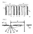
- FIG. 1is a schematic plan view that shows an interconnect layout according to an embodiment of the present invention
- FIG. 2shows the principle of the interconnect layout according to the embodiment
- FIG. 3is a graph that shows a result of using the interconnect layout according to the embodiment.
- FIG. 4is a schematic plan view that shows an interconnect layout according to a conventional technique.
- FIG. 5is a schematic plan view that shows an interconnect layout according to a conventional technique.
- a first gate pattern and a second gate patternprovided substantially in parallel to each other at a first predetermined distance therebetween, a first dummy pattern (dummy interconnect 110 ) that is provided to be adjacent to the first gate pattern on an opposite side to a side on which the second gate pattern is provided at a second predetermined distance from the first gate pattern, in a direction substantially in parallel to a longitudinal direction of the first gate pattern, and that includes no circuitry functions.
- a second dummy pattern(dummy interconnect 111 ) that is provided to be adjacent to the second gate pattern on an opposite side to the side on which the first gate pattern is provided at a third predetermined distance from the second gate pattern, in a direction substantially in parallel to a longitudinal direction of the second gate pattern, and that includes no circuitry functions are arranged.
- FIG. 1is a plan view for describing the interconnect layout 100 of a transistor according to the embodiment of the present invention.
- the interconnect layout 100includes a block 102 and a block 104 , and a dummy interconnect 112 serving as a third dummy pattern.
- the block 102 and the block 104have characteristic that they are not electrically connected to each other and are not equal in potential.
- the block 102includes a designed interconnect 106 , the dummy interconnect 110 serving as the first dummy pattern, and the dummy interconnect 111 serving as the second dummy pattern.
- the block 104includes a designed interconnect 108 , a dummy interconnect 114 serving as a second dummy pattern, and a dummy interconnect 115 serving as a first dummy pattern.
- a part of the designed interconnect 106 located at the left side of a notch portion of the designed interconnect 106 and a part of the designed interconnect 108 located at the right side of a notch portion of the designed interconnect 108are first gate patterns, respectively.
- a part of the designed interconnect 106 located at the right side of a notch portion of the designed interconnect 106 and a part of the designed interconnect 108 located at the left side of a notch portion of the designed interconnect 108are second gate patterns, respectively.
- the designed interconnect 106therefore, includes the first gate pattern and the second gate pattern.
- the designed interconnect 108includes the first gate pattern and the second gate pattern.
- the first gate patternsare arranged substantially in parallel to the second gate patterns.
- the designed interconnect 106is of a U-shape that has the notch open upward
- the designed interconnect 108is of an inverted-U-shape that has the notch open downward in FIG. 1 .
- the dummy interconnect 110is arranged at the left side of the designed interconnect 106 , that is, on the opposite side to the side on which the second gate pattern is provided in the direction substantially in parallel to the longitudinal direction of the first gate pattern.
- the dummy interconnect 111is arranged at the right side of the designed interconnect 106 , that is, on the opposite side to the side on which the first gate pattern is provided in the direction substantially in parallel to the longitudinal direction of the second gate pattern.
- the dummy interconnect 114is arranged at the left side of the designed interconnect 108 , that is, on the opposite side to the side on which the first gate pattern is provided in the direction substantially in parallel to the longitudinal direction of the second gate pattern.
- the dummy interconnect 115is arranged at the right side of the designed interconnect 108 , that is, on the opposite side to the side on the second gate pattern is provided in the direction substantially in parallel to the longitudinal direction of the first gate pattern.
- substantially in parallelmeans that a margin within a range in which advantages of this embodiment are exhibited is allowed when each interconnect is arranged.
- the dummy interconnect 112is arranged at the right side of the dummy interconnect 111 and at the left side of the dummy interconnect 114 , that is, arranged between the block 102 and the block 104 in the direction substantially in parallel to the longitudinal direction of the first gate pattern and to the longitudinal direction of the dummy interconnect 111 .
- the dummy interconnects 111 , 112 , 114 , and 115do not include circuitry functions. Further, in the present embodiment, a length of each dummy interconnect in the longitudinal direction is equal to that of the designed interconnect 106 and the designed interconnect 108 in the longitudinal direction.
- the center-to-center distance P 1 of the designed interconnect 106 and the center-to-center distance P 1 of the designed interconnect 108which distance is referred to as “the first predetermined distance” are 0.38 ⁇ m.
- the center-to-center distance P 2 between the first gate pattern located at the left side of the notch portion of the designed interconnect 106 and the dummy interconnect 110which distance is referred to as “the second predetermined distance” and the center-to-center distance P 3 between the second gate pattern located at the right side of the notch portion of the designed interconnect 106 and the dummy interconnect 111 , which distance is referred to as “the third predetermined distance”
- the center-to-center distance P 2 between the first gate pattern located at the right side of the notch portion of the designed interconnect 108 and the dummy interconnect 115which distance is referred to as “the second predetermined distance” and the center-to-center distance P 3 between the second gate pattern located at the left side of the notch portion of the designed interconnect 108 and the dummy interconnect 115 , which distance is referred to as “the third predetermined distance” are 0.38 ⁇ m.
- a center-to-center distance P 4 between the dummy interconnect 111 and the dummy interconnect 112 and the center-to-center distance P 4 between the dummy interconnect 112 and the dummy interconnect 114are 0.38 ⁇ m.
- the gate patterns and the dummy interconnectsare arranged so that the center-to-center distances P 1 , P 2 , P 3 , and P 4 are all equal and 0.38 ⁇ m.
- the center-to-center distance P 1 of the designed interconnect 106 and that of the designed interconnect 108means a distance between a centerline of the part of the designed interconnect located outside the notch portion thereof serving as the first gate pattern and a centerline of the part of the designed interconnect located inside the notch portion thereof serving as the second gate pattern.
- the interconnect layout 100is exposed to a light using an ArF light source as a laser light source in a photoresist step.
- An exposure wavelength ⁇ of the ArF lightis about 193 nanometers.
- the center-to-center distance (P 1 ) of the designed interconnect 106 and of the designed interconnect 108is 0.38 ⁇ m. Accordingly, the designed interconnect 106 and the designed interconnect 108 are arranged so that a numeric value of P 1 is within a range from ⁇ 5% to +5% of the exposure wavelength ⁇ while centering around a numeric value that is a natural number multiple of the exposure wavelength, which is “P 1 ′”.
- the center-to-center distances (P 2 and P 3 ) between the respective dummy interconnects and the designed interconnectsare equal to P 1 (0.38 ⁇ m). Accordingly, the dummy interconnects 110 , 111 , 114 , and 115 are arranged so that numeric values of P 2 and P 3 are within the range from ⁇ 5% to +5% of the exposure wavelength ⁇ while centering around the numeric value of a natural number multiple of the exposure wavelength, which is “P 2 ′ and P 3 ′”.
- the center-to-center distances (P 4 ) between the dummy interconnect 111 or the dummy interconnect 114are equal to P 1 , P 2 , P 3 (0.38 ⁇ m). Accordingly, the dummy interconnects 114 is arranged so that numeric values of P 4 is within the range from ⁇ 5% to +5% of the exposure wavelength ⁇ while centering around the numeric value of a natural number multiple of the exposure wavelength, which is “P 4 ′”.
- FIG. 2shows the principle of an optical diffraction effect generated when the laser light used for the exposure is incident on a reticle 120 .
- “ ⁇ 2 to +2”indicates that an n th order diffracted light advances in two directions with an extension of the incident light on the reticle 120 set as a centerline.
- Optical diffractioncan be expressed by converting a pattern periodicity into a diffracted light periodicity as shown in the following Equation.
- Sinqm ⁇ /P (where m is a natural number, ⁇ shows the exposure wavelength, P shows the center-to-center distance between the patterns, and q shows a diffraction angle).
- the center-to-center distance between the patternsis set to the numeric value that is a natural number multiple of the exposure wavelength, the diffracted light is reduced. It is, therefore, considered that an angle distribution of the diffracted light is made small and a fluctuation in imaging can be reduced. As a result, fluctuations in shape of the gate patterns generated by repetition of exposure shots can be reduced.
- the fluctuationsare the smallest near 0.38 ⁇ m that is within 5% of the exposure wavelength and that centers around the center-to-center distance which is twice as large as the exposure wavelength. If a light intensity distribution is considered, a big reduction effect of fluctuations is obtained if the “m” is set as small as possible. This is because, the smaller “m” is, the higher the intensity of the light is and the exposure depends on the diffracted light at high intensity more greatly. If “m” is equal to or smaller than 2, in particular, the big reduction effect of fluctuations is obtained.
- the dummy interconnect patternsneed to be arranged substantially in parallel to the designed interconnects.
- the fluctuation width of the center-to-center distance between each gate pattern and each dummy gate patternis within the range from ⁇ 10% to +10% of the center-to-center distance.
- the center-to-center distance P 1 between the gate patterns, and the center-to-center distances P 2 and P 3 between the gate patterns and the dummy interconnectsare equally 0.38 ⁇ m.
- the gate patterns and the dummy interconnectsare arranged so that the center-to-center distances are within the range from ⁇ 5% and +5% of the exposure wavelength ⁇ while centering around the numeric value that is a natural number multiple of the wavelength ⁇ of the ArF light used as the laser light during the exposure.
- the fluctuation width of 10%is specified based on the center-to-center distance.
- the fluctuation widthis specified based on the exposure wavelength ⁇ . Since the exposure wavelength is smaller than the center-to-center distance, the fluctuation width of the center-to-center distance according to the present embodiment is smaller than the fluctuation width according to the conventional technique.
- the fluctuation widthsince the fluctuation width is specified based on the center-to-center distance, the fluctuation width depends on the center-to-center distance and it is, therefore, difficult to accurately specify the fluctuation width.
- the exposure wavelength ⁇since the exposure wavelength ⁇ has no change as long as the laser light source is same, the fluctuation width can be specified more accurately. It is, therefore, possible to more accurately make the angle distribution of the diffracted light smaller and further reduce the fluctuation in imaging. Accordingly, the fluctuations in shape of the gate patterns generated by the repetition of the exposure shots can be reduced further greatly.
- the fluctuation width of the center-to-center distanceis specified based on the exposure wavelength ⁇ . It is, therefore, possible to apply the layout method according to the present embodiment to some exposure apparatus that irradiate any wavelength.
- the dummy interconnect 112 and the dummy interconnect 111 and the dummy interconnect 112 and the dummy interconnect 114are arranged so that the center-to-center distances P 4 therebetween are equally 0.38 ⁇ m similarly to P 1 , P 2 , and P 3 . Because of this, a width of fluctuations in shape of the dummy interconnects due to the exposure shots is substantially equal to that of fluctuations in shape of the designed interconnects. Accordingly, it is possible to further reduce the shape fluctuations on end portions of the designed interconnect 106 and the designed interconnect 108 in their longitudinal directions.
- the instance in which the ArF light (at a wavelength of about 193 nanometers) is used as the laser lighthas been described.
- a laser lightsuch as KrF (at a wavelength of about 248 nanometers) or an i-ray (at a wavelength of about 365 nanometers) larger in wavelength than the ArF light or a laser light such as F 2 (at a wavelength of 157 nanometers) smaller in wavelength than the ArF light may be used as long as the laser light is available in the photoresist step.
- the wavelength of the light source used as the laser lightis smaller, the fluctuation width is smaller. It is, therefore, possible to further reduce the fluctuations in shape of the gate patterns.
- the laser lightis preferably F 2 , ArF, KrF, or i-ray having the wavelength of which is equal to or smaller than 400 nanometers, and more preferably F 2 or ArF having the wavelength of which is equal to or smaller than 200 nanometers.
- the instance in which the center-to-center distances P 1 , P 2 , P 3 , P 4 and the like are equally 0.38 ⁇ mhas been described.
- the numeric value of the center-to-center distanceis within the range from ⁇ 10% to +10% of the numeric value that is a natural number multiple of the exposure wavelength ⁇ , it is possible to reduce the fluctuations in shape of the gate patterns. If the fluctuation width of the center-to-center distance is within the range from ⁇ 5% to +5% of the exposure wavelength ⁇ , it is possible to further reduce the fluctuations in shape of the gate patterns.
- each blockhas been described.
- two or more designed interconnectsmay be present in each block.
- two or more dummy interconnectsmay be present on each side of each designed interconnect.
- each of the designed interconnectsmay be configured by two or more interconnects provided substantially in parallel. In this case, the designed interconnects are assumed to be electrically connected to one another on the other layer within the transistor.
- dummy interconnect 112is held between the block 102 and the block 104 .
- two or more dummy interconnectsmay be held between the blocks.
- a configuration in which no dummy interconnect is held between the block 102 and the block 104 and in which only dummy interconnects are arranged in the respective blocksmay be effectively used.
- the interconnect layout method for the transistorhas been described.
- the interconnect layout method described in this embodimentmay be applied to a semiconductor device other than the transistor.
Landscapes
- Physics & Mathematics (AREA)
- Condensed Matter Physics & Semiconductors (AREA)
- General Physics & Mathematics (AREA)
- Engineering & Computer Science (AREA)
- Computer Hardware Design (AREA)
- Microelectronics & Electronic Packaging (AREA)
- Power Engineering (AREA)
- Preparing Plates And Mask In Photomechanical Process (AREA)
- Design And Manufacture Of Integrated Circuits (AREA)
- Exposure Of Semiconductors, Excluding Electron Or Ion Beam Exposure (AREA)
- Exposure And Positioning Against Photoresist Photosensitive Materials (AREA)
- Semiconductor Integrated Circuits (AREA)
Abstract
Description
Claims (16)
P1=m1λ
P1′−0.1λ≦P1≦P1′+0.1λ,
P2=m2λ
P2′−0.1λ≦P2≦P2′+0.1λ,
P3=m3λ
P3′−0.1λ≦P3≦P3′+0.1λ.
P4=m4λ
P4′−0.1λ≦P4≦P4′+0.1λ.
Applications Claiming Priority (2)
| Application Number | Priority Date | Filing Date | Title |
|---|---|---|---|
| JP2004304309AJP2006119195A (en) | 2004-10-19 | 2004-10-19 | Wiring layout method |
| JP2004-304309 | 2004-10-19 |
Publications (2)
| Publication Number | Publication Date |
|---|---|
| US20060084261A1 US20060084261A1 (en) | 2006-04-20 |
| US7294534B2true US7294534B2 (en) | 2007-11-13 |
Family
ID=36181323
Family Applications (1)
| Application Number | Title | Priority Date | Filing Date |
|---|---|---|---|
| US11/244,137Expired - Fee RelatedUS7294534B2 (en) | 2004-10-19 | 2005-10-06 | Interconnect layout method |
Country Status (2)
| Country | Link |
|---|---|
| US (1) | US7294534B2 (en) |
| JP (1) | JP2006119195A (en) |
Cited By (30)
| Publication number | Priority date | Publication date | Assignee | Title |
|---|---|---|---|---|
| US7842975B2 (en) | 2006-03-09 | 2010-11-30 | Tela Innovations, Inc. | Dynamic array architecture |
| US7888705B2 (en) | 2007-08-02 | 2011-02-15 | Tela Innovations, Inc. | Methods for defining dynamic array section with manufacturing assurance halo and apparatus implementing the same |
| US7932545B2 (en) | 2006-03-09 | 2011-04-26 | Tela Innovations, Inc. | Semiconductor device and associated layouts including gate electrode level region having arrangement of six linear conductive segments with side-to-side spacing less than 360 nanometers |
| US7939443B2 (en) | 2008-03-27 | 2011-05-10 | Tela Innovations, Inc. | Methods for multi-wire routing and apparatus implementing same |
| US7943967B2 (en) | 2006-03-09 | 2011-05-17 | Tela Innovations, Inc. | Semiconductor device and associated layouts including diffusion contact placement restriction based on relation to linear conductive segments |
| US7956421B2 (en) | 2008-03-13 | 2011-06-07 | Tela Innovations, Inc. | Cross-coupled transistor layouts in restricted gate level layout architecture |
| US7979829B2 (en) | 2007-02-20 | 2011-07-12 | Tela Innovations, Inc. | Integrated circuit cell library with cell-level process compensation technique (PCT) application and associated methods |
| US7994545B2 (en) | 2007-10-26 | 2011-08-09 | Tela Innovations, Inc. | Methods, structures, and designs for self-aligning local interconnects used in integrated circuits |
| US8214778B2 (en) | 2007-08-02 | 2012-07-03 | Tela Innovations, Inc. | Methods for cell phasing and placement in dynamic array architecture and implementation of the same |
| US8225261B2 (en) | 2006-03-09 | 2012-07-17 | Tela Innovations, Inc. | Methods for defining contact grid in dynamic array architecture |
| US8225239B2 (en) | 2006-03-09 | 2012-07-17 | Tela Innovations, Inc. | Methods for defining and utilizing sub-resolution features in linear topology |
| US8245180B2 (en) | 2006-03-09 | 2012-08-14 | Tela Innovations, Inc. | Methods for defining and using co-optimized nanopatterns for integrated circuit design and apparatus implementing same |
| US8247846B2 (en) | 2006-03-09 | 2012-08-21 | Tela Innovations, Inc. | Oversized contacts and vias in semiconductor chip defined by linearly constrained topology |
| US8286107B2 (en) | 2007-02-20 | 2012-10-09 | Tela Innovations, Inc. | Methods and systems for process compensation technique acceleration |
| US8448102B2 (en) | 2006-03-09 | 2013-05-21 | Tela Innovations, Inc. | Optimizing layout of irregular structures in regular layout context |
| US8453094B2 (en) | 2008-01-31 | 2013-05-28 | Tela Innovations, Inc. | Enforcement of semiconductor structure regularity for localized transistors and interconnect |
| US8541879B2 (en) | 2007-12-13 | 2013-09-24 | Tela Innovations, Inc. | Super-self-aligned contacts and method for making the same |
| US8653857B2 (en) | 2006-03-09 | 2014-02-18 | Tela Innovations, Inc. | Circuitry and layouts for XOR and XNOR logic |
| US8661392B2 (en) | 2009-10-13 | 2014-02-25 | Tela Innovations, Inc. | Methods for cell boundary encroachment and layouts implementing the Same |
| US8658542B2 (en) | 2006-03-09 | 2014-02-25 | Tela Innovations, Inc. | Coarse grid design methods and structures |
| US8667443B2 (en) | 2007-03-05 | 2014-03-04 | Tela Innovations, Inc. | Integrated circuit cell library for multiple patterning |
| US8839175B2 (en) | 2006-03-09 | 2014-09-16 | Tela Innovations, Inc. | Scalable meta-data objects |
| US8863063B2 (en) | 2009-05-06 | 2014-10-14 | Tela Innovations, Inc. | Finfet transistor circuit |
| US9035359B2 (en) | 2006-03-09 | 2015-05-19 | Tela Innovations, Inc. | Semiconductor chip including region including linear-shaped conductive structures forming gate electrodes and having electrical connection areas arranged relative to inner region between transistors of different types and associated methods |
| US9122832B2 (en) | 2008-08-01 | 2015-09-01 | Tela Innovations, Inc. | Methods for controlling microloading variation in semiconductor wafer layout and fabrication |
| US9159627B2 (en) | 2010-11-12 | 2015-10-13 | Tela Innovations, Inc. | Methods for linewidth modification and apparatus implementing the same |
| US9230910B2 (en) | 2006-03-09 | 2016-01-05 | Tela Innovations, Inc. | Oversized contacts and vias in layout defined by linearly constrained topology |
| US9563733B2 (en) | 2009-05-06 | 2017-02-07 | Tela Innovations, Inc. | Cell circuit and layout with linear finfet structures |
| CN107316861A (en)* | 2016-04-27 | 2017-11-03 | 株式会社村田制作所 | Semiconductor device |
| US10950615B2 (en) | 2018-06-18 | 2021-03-16 | Toshiba Memory Corporation | Semiconductor memory device and manufacturing method thereof |
Families Citing this family (8)
| Publication number | Priority date | Publication date | Assignee | Title |
|---|---|---|---|---|
| US20080001233A1 (en)* | 2006-05-11 | 2008-01-03 | Ashok Kumar Kapoor | Semiconductor device with circuits formed with essentially uniform pattern density |
| GB2439759A (en)* | 2006-06-30 | 2008-01-09 | X Fab Uk Ltd | RF-CMOS transistor array |
| KR100818115B1 (en) | 2007-05-18 | 2008-04-01 | 주식회사 하이닉스반도체 | Layout method of semiconductor device |
| US8053346B2 (en)* | 2007-04-30 | 2011-11-08 | Hynix Semiconductor Inc. | Semiconductor device and method of forming gate and metal line thereof with dummy pattern and auxiliary pattern |
| JP5415710B2 (en)* | 2008-04-10 | 2014-02-12 | ルネサスエレクトロニクス株式会社 | Semiconductor device |
| JP5235936B2 (en) | 2010-05-10 | 2013-07-10 | パナソニック株式会社 | Semiconductor device and layout creation method thereof |
| FR2974235A1 (en)* | 2011-04-15 | 2012-10-19 | St Microelectronics Crolles 2 | Method for forming standard cells that are utilized for implementing e.g. OR boolean function in integrated circuit, involves extending levels along margins of cells to obtain patterns during same photolithography step, respectively |
| US11556691B2 (en)* | 2018-09-28 | 2023-01-17 | Taiwan Semiconductor Manufacturing Company, Ltd. | Track-based fill (TBF) method for metal patterning |
Citations (9)
| Publication number | Priority date | Publication date | Assignee | Title |
|---|---|---|---|---|
| US5459093A (en)* | 1993-03-18 | 1995-10-17 | Sony Corporation | Method for forming dummy pattern in a semiconductor device |
| JPH09311432A (en) | 1996-05-23 | 1997-12-02 | Nec Corp | Pattern forming method for semiconductor device |
| JP2000112114A (en) | 1998-10-08 | 2000-04-21 | Hitachi Ltd | Semiconductor device and method of manufacturing semiconductor device |
| US6261883B1 (en)* | 1997-03-31 | 2001-07-17 | Hitachi, Ltd. | Semiconductor integrated circuit device, and fabrication process and designing method thereof |
| US6413847B1 (en)* | 1999-11-15 | 2002-07-02 | Winbond Electronics Corp. | Method of forming dummy metal pattern |
| US20020179941A1 (en)* | 2001-06-05 | 2002-12-05 | Atsushi Ootake | Semiconductor device and method of manufacturing the same |
| US20040152243A1 (en)* | 2000-11-20 | 2004-08-05 | Kenichi Kuroda | Semiconductor device and a method of manufacturing the same and designing the same |
| US6905967B1 (en)* | 2003-03-31 | 2005-06-14 | Amd, Inc. | Method for improving planarity of shallow trench isolation using multiple simultaneous tiling systems |
| US7153728B2 (en)* | 2002-12-13 | 2006-12-26 | Oki Electric Industry Co., Ltd. | Estimation of remaining film thickness distribution, correction of patterning and insulation film removing masks with remaining film thickness distribution, and production of semiconductor device with corrected patterning and insulation film removing masks |
Family Cites Families (1)
| Publication number | Priority date | Publication date | Assignee | Title |
|---|---|---|---|---|
| JP3759138B2 (en)* | 2003-02-17 | 2006-03-22 | 松下電器産業株式会社 | Photo mask |
- 2004
- 2004-10-19JPJP2004304309Apatent/JP2006119195A/enactivePending
- 2005
- 2005-10-06USUS11/244,137patent/US7294534B2/ennot_activeExpired - Fee Related
Patent Citations (9)
| Publication number | Priority date | Publication date | Assignee | Title |
|---|---|---|---|---|
| US5459093A (en)* | 1993-03-18 | 1995-10-17 | Sony Corporation | Method for forming dummy pattern in a semiconductor device |
| JPH09311432A (en) | 1996-05-23 | 1997-12-02 | Nec Corp | Pattern forming method for semiconductor device |
| US6261883B1 (en)* | 1997-03-31 | 2001-07-17 | Hitachi, Ltd. | Semiconductor integrated circuit device, and fabrication process and designing method thereof |
| JP2000112114A (en) | 1998-10-08 | 2000-04-21 | Hitachi Ltd | Semiconductor device and method of manufacturing semiconductor device |
| US6413847B1 (en)* | 1999-11-15 | 2002-07-02 | Winbond Electronics Corp. | Method of forming dummy metal pattern |
| US20040152243A1 (en)* | 2000-11-20 | 2004-08-05 | Kenichi Kuroda | Semiconductor device and a method of manufacturing the same and designing the same |
| US20020179941A1 (en)* | 2001-06-05 | 2002-12-05 | Atsushi Ootake | Semiconductor device and method of manufacturing the same |
| US7153728B2 (en)* | 2002-12-13 | 2006-12-26 | Oki Electric Industry Co., Ltd. | Estimation of remaining film thickness distribution, correction of patterning and insulation film removing masks with remaining film thickness distribution, and production of semiconductor device with corrected patterning and insulation film removing masks |
| US6905967B1 (en)* | 2003-03-31 | 2005-06-14 | Amd, Inc. | Method for improving planarity of shallow trench isolation using multiple simultaneous tiling systems |
Cited By (194)
| Publication number | Priority date | Publication date | Assignee | Title |
|---|---|---|---|---|
| US8253173B2 (en) | 2006-03-09 | 2012-08-28 | Tela Innovations, Inc. | Semiconductor device with gate level including four transistors of first type and four transistors of second type separated by non-diffusion region and having at least two gate contacts positioned outside separating non-diffusion region |
| US7952119B2 (en) | 2006-03-09 | 2011-05-31 | Tela Innovations, Inc. | Semiconductor device and associated layout having three or more linear-shaped gate electrode level conductive segments of both equal length and equal pitch |
| US7906801B2 (en) | 2006-03-09 | 2011-03-15 | Tela Innovations, Inc. | Semiconductor device and associated layouts having transistors formed from six linear conductive segments with intervening diffusion contact restrictions |
| US8921896B2 (en) | 2006-03-09 | 2014-12-30 | Tela Innovations, Inc. | Integrated circuit including linear gate electrode structures having different extension distances beyond contact |
| US7910958B2 (en) | 2006-03-09 | 2011-03-22 | Tela Innovations, Inc. | Semiconductor device and associated layouts having transistors formed from linear conductive segment with non-active neighboring linear conductive segment |
| US7910959B2 (en) | 2006-03-09 | 2011-03-22 | Tela Innovations, Inc. | Semiconductor device and associated layouts having transistors formed from six linear conductive segments with gate electrode connection through single interconnect level |
| US8946781B2 (en) | 2006-03-09 | 2015-02-03 | Tela Innovations, Inc. | Integrated circuit including gate electrode conductive structures with different extension distances beyond contact |
| US7923757B2 (en) | 2006-03-09 | 2011-04-12 | Tela Innovations, Inc. | Semiconductor device and associated layouts having linear shaped gate electrodes defined along at least five adjacent gate electrode tracks of equal pitch with gate electrode connection through single interconnect level |
| US7932545B2 (en) | 2006-03-09 | 2011-04-26 | Tela Innovations, Inc. | Semiconductor device and associated layouts including gate electrode level region having arrangement of six linear conductive segments with side-to-side spacing less than 360 nanometers |
| US7932544B2 (en) | 2006-03-09 | 2011-04-26 | Tela Innovations, Inc. | Semiconductor device and associated layouts including linear conductive segments having non-gate extension portions |
| US8839175B2 (en) | 2006-03-09 | 2014-09-16 | Tela Innovations, Inc. | Scalable meta-data objects |
| US7943966B2 (en) | 2006-03-09 | 2011-05-17 | Tela Innovations, Inc. | Integrated circuit and associated layout with gate electrode level portion including at least two complimentary transistor forming linear conductive segments and at least one non-gate linear conductive segment |
| US7943967B2 (en) | 2006-03-09 | 2011-05-17 | Tela Innovations, Inc. | Semiconductor device and associated layouts including diffusion contact placement restriction based on relation to linear conductive segments |
| US7948013B2 (en) | 2006-03-09 | 2011-05-24 | Tela Innovations, Inc. | Semiconductor device and associated layouts having linear shaped gate electrodes defined along at least five adjacent gate electrode tracks of equal pitch |
| US7948012B2 (en) | 2006-03-09 | 2011-05-24 | Tela Innovations, Inc. | Semiconductor device having 1965 nm gate electrode level region including at least four active linear conductive segments and at least one non-gate linear conductive segment |
| US8258547B2 (en) | 2006-03-09 | 2012-09-04 | Tela Innovations, Inc. | Semiconductor device with linearly restricted gate level region including two transistors of first type and two transistors of second type with offset gate contacts |
| US8952425B2 (en) | 2006-03-09 | 2015-02-10 | Tela Innovations, Inc. | Integrated circuit including at least four linear-shaped conductive structures having extending portions of different length |
| US8823062B2 (en) | 2006-03-09 | 2014-09-02 | Tela Innovations, Inc. | Integrated circuit with offset line end spacings in linear gate electrode level |
| US7989848B2 (en) | 2006-03-09 | 2011-08-02 | Tela Innovations, Inc. | Semiconductor device having at least four side-by-side electrodes of equal length and equal pitch with at least two transistor connections to power or ground |
| US7989847B2 (en) | 2006-03-09 | 2011-08-02 | Tela Innovations, Inc. | Semiconductor device having linear-shaped gate electrodes of different transistor types with uniformity extending portions of different lengths |
| US9009641B2 (en) | 2006-03-09 | 2015-04-14 | Tela Innovations, Inc. | Circuits with linear finfet structures |
| US8022441B2 (en) | 2006-03-09 | 2011-09-20 | Tela Innovations, Inc. | Semiconductor device and associated layouts having transistors formed from six linear conductive segments with gate electrode-to-gate electrode connection through single interconnect level and common node connection through different interconnect level |
| US8030689B2 (en) | 2006-03-09 | 2011-10-04 | Tela Innovations, Inc. | Integrated circuit device and associated layout including separated diffusion regions of different type each having four gate electrodes with each of two complementary gate electrode pairs formed from respective linear conductive segment |
| US8035133B2 (en) | 2006-03-09 | 2011-10-11 | Tela Innovations, Inc. | Semiconductor device having two pairs of transistors of different types formed from shared linear-shaped conductive features with intervening transistors of common type on equal pitch |
| US8058671B2 (en) | 2006-03-09 | 2011-11-15 | Tela Innovations, Inc. | Semiconductor device having at least three linear-shaped electrode level conductive features of equal length positioned side-by-side at equal pitch |
| US10230377B2 (en) | 2006-03-09 | 2019-03-12 | Tela Innovations, Inc. | Circuitry and layouts for XOR and XNOR logic |
| US8072003B2 (en) | 2006-03-09 | 2011-12-06 | Tela Innovations, Inc. | Integrated circuit device and associated layout including two pairs of co-aligned complementary gate electrodes with offset gate contact structures |
| US8089104B2 (en) | 2006-03-09 | 2012-01-03 | Tela Innovations, Inc. | Integrated circuit with gate electrode level region including multiple linear-shaped conductive structures forming gate electrodes of transistors and including uniformity extending portions of different size |
| US8089100B2 (en) | 2006-03-09 | 2012-01-03 | Tela Innovations, Inc. | Integrated circuit with gate electrode level region including at least four linear-shaped conductive structures forming gate electrodes of transistors and including extending portions of at least two different sizes |
| US8088681B2 (en) | 2006-03-09 | 2012-01-03 | Tela Innovations, Inc. | Method for fabricating integrated circuit including separated diffusion regions of different type each having four gate electrodes with each of two complementary gate electrode pairs formed from respective linear condcutive segment |
| US8088682B2 (en) | 2006-03-09 | 2012-01-03 | Tela Innovations, Inc. | Method for fabricating integrated circuit with gate electrode level region including two side-by-side ones of at least three linear-shaped conductive structures electrically connected to each other through non-gate level |
| US8089099B2 (en) | 2006-03-09 | 2012-01-03 | Tela Innovations, Inc, | Integrated circuit device and associated layout including gate electrode level region of 965 NM radius with linear-shaped conductive segments on fixed pitch |
| US8089098B2 (en) | 2006-03-09 | 2012-01-03 | Tela Innovations, Inc. | Integrated circuit device and associated layout including linear gate electrodes of different transistor types next to linear-shaped non-gate conductive segment |
| US8089103B2 (en) | 2006-03-09 | 2012-01-03 | Tela Innovations, Inc. | Integrated circuit device with gate level region including at least three linear-shaped conductive segments having offset line ends and forming three transistors of first type and one transistor of second type |
| US8089101B2 (en) | 2006-03-09 | 2012-01-03 | Tela Innovations, Inc. | Integrated circuit device with gate electrode level region including two side-by-side ones of at least three linear-shaped conductive structures electrically connected to each other through non-gate level |
| US8088680B2 (en) | 2006-03-09 | 2012-01-03 | Tela Innovations, Inc. | Method for fabricating integrated circuit having at least three linear-shaped gate electrode level conductive features of equal length positioned side-by-side at equal pitch |
| US8088679B2 (en) | 2006-03-09 | 2012-01-03 | Tela Innovations, Inc. | Method for fabricating integrated circuit with gate electrode level portion including at least two complementary transistor forming linear conductive segments and at least one non-gate linear conductive segment |
| US8089102B2 (en) | 2006-03-09 | 2012-01-03 | Tela Innovations, Inc. | Method for fabricating integrated circuit having three or more linear-shaped gate electrode level conductive segments of both equal length and equal pitch |
| US8101975B2 (en) | 2006-03-09 | 2012-01-24 | Tela Innovations, Inc. | Integrated circuit device with gate level region including non-gate linear conductive segment positioned within 965 nanometers of four transistors of first type and four transistors of second type |
| US8110854B2 (en) | 2006-03-09 | 2012-02-07 | Tela Innovations, Inc. | Integrated circuit device with linearly defined gate electrode level region and shared diffusion region of first type connected to shared diffusion region of second type through at least two interconnect levels |
| US8129750B2 (en) | 2006-03-09 | 2012-03-06 | Tela Innovations, Inc. | Integrated circuit including at least six linear-shaped conductive structures forming gate electrodes of transistors with at least two linear-shaped conductive structures of different length |
| US8129751B2 (en) | 2006-03-09 | 2012-03-06 | Tela Innovations, Inc. | Integrated circuit including at least six linear-shaped conductive structures forming gate electrodes and including four conductive contacting structures having at least two different connection distances |
| US8129819B2 (en) | 2006-03-09 | 2012-03-06 | Tela Innovations, Inc. | Method of fabricating integrated circuit including at least six linear-shaped conductive structures at equal pitch including at least two linear-shaped conductive structures having non-gate portions of different length |
| US8129757B2 (en) | 2006-03-09 | 2012-03-06 | Tela Innovations, Inc. | Integrated circuit including at least six linear-shaped conductive structive structures at equal pitch including at least two linear-shaped conductive structures having non-gate portions of different length |
| US8129756B2 (en) | 2006-03-09 | 2012-03-06 | Tela Innovations, Inc. | Integrated circuit including at least six linear-shaped conductive structures forming gate electrodes of transistors with at least two different extension distances beyond conductive contacting structures |
| US8129755B2 (en) | 2006-03-09 | 2012-03-06 | Tela Innovations, Inc. | Integrated circuit with gate electrode level including at least four linear-shaped conductive structures of equal length and equal pitch with linear-shaped conductive structure forming one transistor |
| US8129754B2 (en) | 2006-03-09 | 2012-03-06 | Tela Innovations, Inc. | Integrated circuit with gate electrode level including at least six linear-shaped conductive structures forming gate electrodes of transisters with at least one pair of linear-shaped conductive structures having offset ends |
| US8129753B2 (en) | 2006-03-09 | 2012-03-06 | Tela Innovations, Inc. | Integrated circuit including gate electrode level region including at least seven linear-shaped conductive structures of equal length positioned at equal pitch with at least two linear-shaped conductive structures each forming one transistor and having extending portion sized greater than gate portion |
| US8129752B2 (en) | 2006-03-09 | 2012-03-06 | Tela Innovations, Inc. | Integrated circuit including a linear-shaped conductive structure forming one gate electrode and having length greater than or equal to one-half the length of linear-shaped conductive structure forming two gate electrodes |
| US8134186B2 (en) | 2006-03-09 | 2012-03-13 | Tela Innovations, Inc. | Integrated circuit including at least three linear-shaped conductive structures at equal pitch including linear-shaped conductive structure having non-gate portion length greater than gate portion length |
| US8134185B2 (en) | 2006-03-09 | 2012-03-13 | Tela Innovations, Inc. | Integrated circuit having gate electrode level region including at least seven linear-shaped conductive structures at equal pitch including linear-shaped conductive structure forming transistors of two different types and at least three linear-shaped conductive structures having aligned ends |
| US8134184B2 (en) | 2006-03-09 | 2012-03-13 | Tela Innovations, Inc. | Integrated circuit having gate electrode level region including at least four linear-shaped conductive structures with some outer-contacted linear-shaped conductive structures having larger outer extending portion than inner extending portion |
| US8134183B2 (en) | 2006-03-09 | 2012-03-13 | Tela Innovations, Inc. | Integrated circuit including linear-shaped conductive structures that have gate portions and extending portions of different size |
| US8138525B2 (en) | 2006-03-09 | 2012-03-20 | Tela Innovations, Inc. | Integrated circuit including at least three linear-shaped conductive structures of different length each forming gate of different transistor |
| US8198656B2 (en) | 2006-03-09 | 2012-06-12 | Tela Innovations, Inc. | Integrated circuit including gate electrode level region including at least four linear-shaped conductive structures of equal length having aligned ends and positioned at equal pitch and forming multiple gate electrodes of transistors of different type |
| US8207053B2 (en) | 2006-03-09 | 2012-06-26 | Tela Innovations, Inc. | Electrodes of transistors with at least two linear-shaped conductive structures of different length |
| US9035359B2 (en) | 2006-03-09 | 2015-05-19 | Tela Innovations, Inc. | Semiconductor chip including region including linear-shaped conductive structures forming gate electrodes and having electrical connection areas arranged relative to inner region between transistors of different types and associated methods |
| US8217428B2 (en) | 2006-03-09 | 2012-07-10 | Tela Innovations, Inc. | Integrated circuit including gate electrode level region including at least three linear-shaped conductive structures of equal length having aligned ends and positioned at equal pitch and forming multiple gate electrodes of transistors of different type |
| US8225261B2 (en) | 2006-03-09 | 2012-07-17 | Tela Innovations, Inc. | Methods for defining contact grid in dynamic array architecture |
| US8225239B2 (en) | 2006-03-09 | 2012-07-17 | Tela Innovations, Inc. | Methods for defining and utilizing sub-resolution features in linear topology |
| US8245180B2 (en) | 2006-03-09 | 2012-08-14 | Tela Innovations, Inc. | Methods for defining and using co-optimized nanopatterns for integrated circuit design and apparatus implementing same |
| US8247846B2 (en) | 2006-03-09 | 2012-08-21 | Tela Innovations, Inc. | Oversized contacts and vias in semiconductor chip defined by linearly constrained topology |
| US9230910B2 (en) | 2006-03-09 | 2016-01-05 | Tela Innovations, Inc. | Oversized contacts and vias in layout defined by linearly constrained topology |
| US8258552B2 (en) | 2006-03-09 | 2012-09-04 | Tela Innovations, Inc. | Semiconductor device including at least six transistor forming linear shapes with at least two transistor forming linear shapes having offset ends |
| US8921897B2 (en) | 2006-03-09 | 2014-12-30 | Tela Innovations, Inc. | Integrated circuit with gate electrode conductive structures having offset ends |
| US8258549B2 (en) | 2006-03-09 | 2012-09-04 | Tela Innovations, Inc. | Semiconductor device including two transistors of first type having gates formed by conductors of different length respectively aligned with two transistors of second type having gates formed by conductors of different length |
| US8253172B2 (en) | 2006-03-09 | 2012-08-28 | Tela Innovations, Inc. | Semiconductor device with linearly restricted gate level region including four serially connected transistors of first type and four serially connected transistors of second type separated by non-diffusion region |
| US8258548B2 (en) | 2006-03-09 | 2012-09-04 | Tela Innovations, Inc. | Semiconductor device with gate level including four transistors of first type and four transistors of second type separated by non-diffusion region with restricted gate contact placement over separating non-diffusion region |
| US8258550B2 (en) | 2006-03-09 | 2012-09-04 | Tela Innovations, Inc. | Semiconductor device including at least six transistor forming linear shapes including at least two transistor forming linear shapes having different extension distances beyond gate contact |
| US10217763B2 (en) | 2006-03-09 | 2019-02-26 | Tela Innovations, Inc. | Semiconductor chip having region including gate electrode features of rectangular shape on gate horizontal grid and first-metal structures of rectangular shape on at least eight first-metal gridlines of first-metal vertical grid |
| US8258551B2 (en) | 2006-03-09 | 2012-09-04 | Tela Innovations, Inc. | Semiconductor device with gate level including transistors of first type and transistors of second type with corresponding gate contact placement restriction |
| US8264007B2 (en) | 2006-03-09 | 2012-09-11 | Tela Innovations, Inc. | Semiconductor device including at least six transistor forming linear shapes including at least two different gate contact connection distances |
| US8264008B2 (en) | 2006-03-09 | 2012-09-11 | Tela Innovations, Inc. | Semiconductor device including transistor forming linear shapes including gate portions and extending portions of different size |
| US10186523B2 (en) | 2006-03-09 | 2019-01-22 | Tela Innovations, Inc. | Semiconductor chip having region including gate electrode features formed in part from rectangular layout shapes on gate horizontal grid and first-metal structures formed in part from rectangular layout shapes on at least eight first-metal gridlines of first-metal vertical grid |
| US8264009B2 (en) | 2006-03-09 | 2012-09-11 | Tela Innovations, Inc. | Semiconductor device with linearly restricted gate level region including four transistors of first type and four transistors of second type with gate defining shapes of different length |
| US10141335B2 (en) | 2006-03-09 | 2018-11-27 | Tela Innovations, Inc. | Semiconductor CIP including region having rectangular-shaped gate structures and first metal structures |
| US10141334B2 (en) | 2006-03-09 | 2018-11-27 | Tela Innovations, Inc. | Semiconductor chip including region having rectangular-shaped gate structures and first-metal structures |
| US9240413B2 (en) | 2006-03-09 | 2016-01-19 | Tela Innovations, Inc. | Methods, structures, and designs for self-aligning local interconnects used in integrated circuits |
| US9336344B2 (en) | 2006-03-09 | 2016-05-10 | Tela Innovations, Inc. | Coarse grid design methods and structures |
| US9425145B2 (en) | 2006-03-09 | 2016-08-23 | Tela Innovations, Inc. | Oversized contacts and vias in layout defined by linearly constrained topology |
| US9425273B2 (en) | 2006-03-09 | 2016-08-23 | Tela Innovations, Inc. | Semiconductor chip including integrated circuit including at least five gate level conductive structures having particular spatial and electrical relationship and method for manufacturing the same |
| US9917056B2 (en) | 2006-03-09 | 2018-03-13 | Tela Innovations, Inc. | Coarse grid design methods and structures |
| US9425272B2 (en) | 2006-03-09 | 2016-08-23 | Tela Innovations, Inc. | Semiconductor chip including integrated circuit including four transistors of first transistor type and four transistors of second transistor type with electrical connections between various transistors and methods for manufacturing the same |
| US8436400B2 (en) | 2006-03-09 | 2013-05-07 | Tela Innovations, Inc. | Semiconductor device with gate level including gate electrode conductors for transistors of first type and transistors of second type with some gate electrode conductors of different length |
| US8448102B2 (en) | 2006-03-09 | 2013-05-21 | Tela Innovations, Inc. | Optimizing layout of irregular structures in regular layout context |
| US9443947B2 (en) | 2006-03-09 | 2016-09-13 | Tela Innovations, Inc. | Semiconductor chip including region having integrated circuit transistor gate electrodes formed by various conductive structures of specified shape and position and method for manufacturing the same |
| US9905576B2 (en) | 2006-03-09 | 2018-02-27 | Tela Innovations, Inc. | Semiconductor chip including region having rectangular-shaped gate structures and first metal structures |
| US8658542B2 (en) | 2006-03-09 | 2014-02-25 | Tela Innovations, Inc. | Coarse grid design methods and structures |
| US9589091B2 (en) | 2006-03-09 | 2017-03-07 | Tela Innovations, Inc. | Scalable meta-data objects |
| US9859277B2 (en) | 2006-03-09 | 2018-01-02 | Tela Innovations, Inc. | Methods, structures, and designs for self-aligning local interconnects used in integrated circuits |
| US8653857B2 (en) | 2006-03-09 | 2014-02-18 | Tela Innovations, Inc. | Circuitry and layouts for XOR and XNOR logic |
| US9754878B2 (en) | 2006-03-09 | 2017-09-05 | Tela Innovations, Inc. | Semiconductor chip including a chip level based on a layout that includes both regular and irregular wires |
| US9741719B2 (en) | 2006-03-09 | 2017-08-22 | Tela Innovations, Inc. | Methods, structures, and designs for self-aligning local interconnects used in integrated circuits |
| US7842975B2 (en) | 2006-03-09 | 2010-11-30 | Tela Innovations, Inc. | Dynamic array architecture |
| US9711495B2 (en) | 2006-03-09 | 2017-07-18 | Tela Innovations, Inc. | Oversized contacts and vias in layout defined by linearly constrained topology |
| US9673825B2 (en) | 2006-03-09 | 2017-06-06 | Tela Innovations, Inc. | Circuitry and layouts for XOR and XNOR logic |
| US8286107B2 (en) | 2007-02-20 | 2012-10-09 | Tela Innovations, Inc. | Methods and systems for process compensation technique acceleration |
| US7979829B2 (en) | 2007-02-20 | 2011-07-12 | Tela Innovations, Inc. | Integrated circuit cell library with cell-level process compensation technique (PCT) application and associated methods |
| US8667443B2 (en) | 2007-03-05 | 2014-03-04 | Tela Innovations, Inc. | Integrated circuit cell library for multiple patterning |
| US9633987B2 (en) | 2007-03-05 | 2017-04-25 | Tela Innovations, Inc. | Integrated circuit cell library for multiple patterning |
| US10074640B2 (en)* | 2007-03-05 | 2018-09-11 | Tela Innovations, Inc. | Integrated circuit cell library for multiple patterning |
| US20170229441A1 (en)* | 2007-03-05 | 2017-08-10 | Tela Innovations, Inc. | Integrated Circuit Cell Library for Multiple Patterning |
| US8966424B2 (en) | 2007-03-07 | 2015-02-24 | Tela Innovations, Inc. | Methods for cell phasing and placement in dynamic array architecture and implementation of the same |
| US9424387B2 (en) | 2007-03-07 | 2016-08-23 | Tela Innovations, Inc. | Methods for cell phasing and placement in dynamic array architecture and implementation of the same |
| US9595515B2 (en) | 2007-03-07 | 2017-03-14 | Tela Innovations, Inc. | Semiconductor chip including integrated circuit defined within dynamic array section |
| US9910950B2 (en) | 2007-03-07 | 2018-03-06 | Tela Innovations, Inc. | Methods for cell phasing and placement in dynamic array architecture and implementation of the same |
| US8549455B2 (en) | 2007-08-02 | 2013-10-01 | Tela Innovations, Inc. | Methods for cell phasing and placement in dynamic array architecture and implementation of the same |
| US7917879B2 (en) | 2007-08-02 | 2011-03-29 | Tela Innovations, Inc. | Semiconductor device with dynamic array section |
| US8283701B2 (en) | 2007-08-02 | 2012-10-09 | Tela Innovations, Inc. | Semiconductor device with dynamic array sections defined and placed according to manufacturing assurance halos |
| US7908578B2 (en) | 2007-08-02 | 2011-03-15 | Tela Innovations, Inc. | Methods for designing semiconductor device with dynamic array section |
| US8214778B2 (en) | 2007-08-02 | 2012-07-03 | Tela Innovations, Inc. | Methods for cell phasing and placement in dynamic array architecture and implementation of the same |
| US8356268B2 (en) | 2007-08-02 | 2013-01-15 | Tela Innovations, Inc. | Integrated circuit device including dynamic array section with gate level having linear conductive features on at least three side-by-side lines and uniform line end spacings |
| US8756551B2 (en) | 2007-08-02 | 2014-06-17 | Tela Innovations, Inc. | Methods for designing semiconductor device with dynamic array section |
| US7888705B2 (en) | 2007-08-02 | 2011-02-15 | Tela Innovations, Inc. | Methods for defining dynamic array section with manufacturing assurance halo and apparatus implementing the same |
| US8759882B2 (en) | 2007-08-02 | 2014-06-24 | Tela Innovations, Inc. | Semiconductor device with dynamic array sections defined and placed according to manufacturing assurance halos |
| US8680626B2 (en) | 2007-10-26 | 2014-03-25 | Tela Innovations, Inc. | Methods, structures, and designs for self-aligning local interconnects used in integrated circuits |
| US10734383B2 (en) | 2007-10-26 | 2020-08-04 | Tela Innovations, Inc. | Methods, structures, and designs for self-aligning local interconnects used in integrated circuits |
| US7994545B2 (en) | 2007-10-26 | 2011-08-09 | Tela Innovations, Inc. | Methods, structures, and designs for self-aligning local interconnects used in integrated circuits |
| US9281371B2 (en) | 2007-12-13 | 2016-03-08 | Tela Innovations, Inc. | Super-self-aligned contacts and method for making the same |
| US10461081B2 (en) | 2007-12-13 | 2019-10-29 | Tel Innovations, Inc. | Super-self-aligned contacts and method for making the same |
| US8951916B2 (en) | 2007-12-13 | 2015-02-10 | Tela Innovations, Inc. | Super-self-aligned contacts and method for making the same |
| US8541879B2 (en) | 2007-12-13 | 2013-09-24 | Tela Innovations, Inc. | Super-self-aligned contacts and method for making the same |
| US9818747B2 (en) | 2007-12-13 | 2017-11-14 | Tela Innovations, Inc. | Super-self-aligned contacts and method for making the same |
| US9202779B2 (en) | 2008-01-31 | 2015-12-01 | Tela Innovations, Inc. | Enforcement of semiconductor structure regularity for localized transistors and interconnect |
| US9530734B2 (en) | 2008-01-31 | 2016-12-27 | Tela Innovations, Inc. | Enforcement of semiconductor structure regularity for localized transistors and interconnect |
| US8701071B2 (en) | 2008-01-31 | 2014-04-15 | Tela Innovations, Inc. | Enforcement of semiconductor structure regularity for localized transistors and interconnect |
| US8453094B2 (en) | 2008-01-31 | 2013-05-28 | Tela Innovations, Inc. | Enforcement of semiconductor structure regularity for localized transistors and interconnect |
| US8581303B2 (en) | 2008-03-13 | 2013-11-12 | Tela Innovations, Inc. | Integrated circuit including cross-coupled trasistors having gate electrodes formed within gate level feature layout channels with four inside positioned gate contacts having offset relationships and electrical connection of cross-coupled transistors through same interconnect layer |
| US9536899B2 (en) | 2008-03-13 | 2017-01-03 | Tela Innovations, Inc. | Semiconductor chip including integrated circuit having cross-coupled transistor configuration and method for manufacturing the same |
| US10727252B2 (en) | 2008-03-13 | 2020-07-28 | Tela Innovations, Inc. | Semiconductor chip including integrated circuit having cross-coupled transistor configuration and method for manufacturing the same |
| US8866197B2 (en) | 2008-03-13 | 2014-10-21 | Tela Innovations, Inc. | Integrated circuit including cross-coupled transistors having gate electrodes formed within gate level feature layout channels with at least two gate electrodes electrically connected to each other through another transistor forming gate level feature |
| US8872283B2 (en) | 2008-03-13 | 2014-10-28 | Tela Innovations, Inc. | Integrated circuit including cross-coupled transistors having gate electrodes formed within gate level feature layout channels with shared diffusion regions on opposite sides of two-transistor-forming gate level feature |
| US8853794B2 (en) | 2008-03-13 | 2014-10-07 | Tela Innovations, Inc. | Integrated circuit within semiconductor chip including cross-coupled transistor configuration |
| US8847329B2 (en) | 2008-03-13 | 2014-09-30 | Tela Innovations, Inc. | Cross-coupled transistor circuit defined having diffusion regions of common node on opposing sides of same gate electrode track with at least two non-inner positioned gate contacts |
| US8847331B2 (en) | 2008-03-13 | 2014-09-30 | Tela Innovations, Inc. | Semiconductor chip including region having cross-coupled transistor configuration with offset electrical connection areas on gate electrode forming conductive structures and at least two different inner extension distances of gate electrode forming conductive structures |
| US8835989B2 (en) | 2008-03-13 | 2014-09-16 | Tela Innovations, Inc. | Integrated circuit including cross-coupled transistors having gate electrodes formed within gate level feature layout channels with gate electrode placement specifications |
| US8836045B2 (en) | 2008-03-13 | 2014-09-16 | Tela Innovations, Inc. | Cross-coupled transistor circuit having diffusion regions of common node on opposing sides of same gate electrode track |
| US8816402B2 (en) | 2008-03-13 | 2014-08-26 | Tela Innovations, Inc. | Integrated circuit including cross-coupled transistors having gate electrodes formed within gate level feature layout channels with gate level feature layout channel including single transistor |
| US8785979B2 (en) | 2008-03-13 | 2014-07-22 | Tela Innovations, Inc. | Integrated circuit including cross-coupled transistors having gate electrodes formed within gate level feature layout channels with two inside positioned gate contacts and two outside positioned gate contacts and electrical connection of cross-coupled transistors through same interconnect layer |
| US8785978B2 (en) | 2008-03-13 | 2014-07-22 | Tela Innovations, Inc. | Integrated circuit including cross-coupled transistors having gate electrodes formed within gate level feature layout channels with electrical connection of cross-coupled transistors through same interconnect layer |
| US9081931B2 (en) | 2008-03-13 | 2015-07-14 | Tela Innovations, Inc. | Cross-coupled transistor circuit having diffusion regions of common node on opposing sides of same gate electrode track and gate node connection through single interconnect layer |
| US9117050B2 (en) | 2008-03-13 | 2015-08-25 | Tela Innovations, Inc. | Integrated circuit including cross-coupled transistors having gate electrodes formed within gate level feature layout channels with gate contact position and offset specifications |
| US10658385B2 (en) | 2008-03-13 | 2020-05-19 | Tela Innovations, Inc. | Cross-coupled transistor circuit defined on four gate electrode tracks |
| US10651200B2 (en) | 2008-03-13 | 2020-05-12 | Tela Innovations, Inc. | Cross-coupled transistor circuit defined on three gate electrode tracks |
| US8772839B2 (en) | 2008-03-13 | 2014-07-08 | Tela Innovations, Inc. | Integrated circuit including cross-coupled transistors having gate electrodes formed within gate level feature layout channels with four inside positioned gate contacts having offset and aligned relationships and electrical connection of transistor gates through linear interconnect conductors in single interconnect layer |
| US9208279B2 (en) | 2008-03-13 | 2015-12-08 | Tela Innovations, Inc. | Semiconductor chip including digital logic circuit including linear-shaped conductive structures having electrical connection areas located within inner region between transistors of different type and associated methods |
| US9213792B2 (en) | 2008-03-13 | 2015-12-15 | Tela Innovations, Inc. | Semiconductor chip including digital logic circuit including at least six transistors with some transistors forming cross-coupled transistor configuration and associated methods |
| US7956421B2 (en) | 2008-03-13 | 2011-06-07 | Tela Innovations, Inc. | Cross-coupled transistor layouts in restricted gate level layout architecture |
| US8742463B2 (en) | 2008-03-13 | 2014-06-03 | Tela Innovations, Inc. | Integrated circuit including cross-coupled transistors having gate electrodes formed within gate level feature layout channels with outer positioned gate contacts |
| US9245081B2 (en) | 2008-03-13 | 2016-01-26 | Tela Innovations, Inc. | Semiconductor chip including digital logic circuit including at least nine linear-shaped conductive structures collectively forming gate electrodes of at least six transistors with some transistors forming cross-coupled transistor configuration and associated methods |
| US8058691B2 (en) | 2008-03-13 | 2011-11-15 | Tela Innovations, Inc. | Semiconductor device including cross-coupled transistors formed from linear-shaped gate level features |
| US8742462B2 (en) | 2008-03-13 | 2014-06-03 | Tela Innovations, Inc. | Integrated circuit including cross-coupled transistors having gate electrodes formed within gate level feature layout channels with gate contact position specifications |
| US8735944B2 (en) | 2008-03-13 | 2014-05-27 | Tela Innovations, Inc. | Integrated circuit including cross-coupled transistors having gate electrodes formed within gate level feature layout channels with serially connected transistors |
| US8258581B2 (en) | 2008-03-13 | 2012-09-04 | Tela Innovations, Inc. | Integrated circuit including cross-coupled transistors with two transistors of different type formed by same gate level structure and two transistors of different type formed by separate gate level structures |
| US8735995B2 (en) | 2008-03-13 | 2014-05-27 | Tela Innovations, Inc. | Cross-coupled transistor circuit defined on three gate electrode tracks with diffusion regions of common node on opposing sides of same gate electrode track |
| US8729643B2 (en) | 2008-03-13 | 2014-05-20 | Tela Innovations, Inc. | Cross-coupled transistor circuit including offset inner gate contacts |
| US8729606B2 (en) | 2008-03-13 | 2014-05-20 | Tela Innovations, Inc. | Integrated circuit including cross-coupled transistors having gate electrodes formed within gate level feature layout channels |
| US8680583B2 (en) | 2008-03-13 | 2014-03-25 | Tela Innovations, Inc. | Integrated circuit including cross-coupled transistors having gate electrodes formed within at least nine gate level feature layout channels |
| US8669595B2 (en) | 2008-03-13 | 2014-03-11 | Tela Innovations, Inc. | Integrated circuit including cross-coupled transistors having gate electrodes formed within gate level feature layout channels with gate contact position, alignment, and offset specifications |
| US8669594B2 (en) | 2008-03-13 | 2014-03-11 | Tela Innovations, Inc. | Integrated circuit including cross-coupled transistors having gate electrodes formed within at least twelve gate level feature layout channels |
| US8264049B2 (en) | 2008-03-13 | 2012-09-11 | Tela Innovations, Inc. | Integrated circuit including cross-coupled transistors with two transistors of different type having gate electrodes formed by common gate level feature with shared diffusion regions on opposite sides of common gate level feature |
| US8853793B2 (en) | 2008-03-13 | 2014-10-07 | Tela Innovations, Inc. | Integrated circuit including gate electrode level region including cross-coupled transistors having gate contacts located over inner portion of gate electrode level region and offset gate level feature line ends |
| US8264044B2 (en) | 2008-03-13 | 2012-09-11 | Tela Innovations, Inc. | Integrated circuit including cross-coupled transistors having two complementary pairs of co-aligned gate electrodes with offset contacting structures positioned between transistors of different type |
| US8274099B2 (en) | 2008-03-13 | 2012-09-25 | Tela Innovations, Inc. | Integrated circuit including cross-coupled transistors having gate electrodes formed within gate level feature layout channels with gate contact position and offset specifications |
| US8592872B2 (en) | 2008-03-13 | 2013-11-26 | Tela Innovations, Inc. | Integrated circuit including cross-coupled transistors with two transistors of different type having gate electrodes formed by common gate level feature with shared diffusion regions on opposite sides of common gate level feature |
| US8587034B2 (en) | 2008-03-13 | 2013-11-19 | Tela Innovations, Inc. | Integrated circuit including cross-coupled transistors having gate electrodes formed within gate level feature layout channels with four inside positioned gate contacts and electrical connection of transistor gates through linear interconnect conductors in single interconnect layer |
| US8581304B2 (en) | 2008-03-13 | 2013-11-12 | Tela Innovations, Inc. | Integrated circuit including cross-coupled transistors having gate electrodes formed within gate level feature layout channels with four inside positioned gate contacts having offset and aligned relationships |
| US8395224B2 (en) | 2008-03-13 | 2013-03-12 | Tela Innovations, Inc. | Linear gate level cross-coupled transistor device with non-overlapping PMOS transistors and non-overlapping NMOS transistors relative to directions of gate electrodes |
| US8575706B2 (en) | 2008-03-13 | 2013-11-05 | Tela Innovations, Inc. | Integrated circuit including cross-coupled transistors having gate electrodes formed within gate level feature layout channels with at least two different gate level features inner extensions beyond gate electrode |
| US8569841B2 (en) | 2008-03-13 | 2013-10-29 | Tela Innovations, Inc. | Integrated circuit including cross-coupled transistors having gate electrodes formed within gate level feature layout channels with at least one gate level feature extending into adjacent gate level feature layout channel |
| US8564071B2 (en) | 2008-03-13 | 2013-10-22 | Tela Innovations, Inc. | Integrated circuit including cross-coupled transistors having gate electrodes formed within gate level feature layout channels with at least two different gate level feature extensions beyond contact |
| US8558322B2 (en) | 2008-03-13 | 2013-10-15 | Tela Innovations, Inc. | Integrated circuit including cross-coupled transistors having gate electrodes formed within gate level feature layout channels with at least two gate electrodes electrically connected to each other through gate level feature |
| US10020321B2 (en) | 2008-03-13 | 2018-07-10 | Tela Innovations, Inc. | Cross-coupled transistor circuit defined on two gate electrode tracks |
| US8405163B2 (en) | 2008-03-13 | 2013-03-26 | Tela Innovations, Inc. | Integrated circuit including cross-coupled transistors having gate electrodes formed within gate level feature layout channels with shared diffusion regions on opposite sides of two-transistor-forming gate level feature |
| US8552509B2 (en) | 2008-03-13 | 2013-10-08 | Tela Innovations, Inc. | Integrated circuit including cross-coupled transistors having gate electrodes formed within gate level feature layout channels with other transistors positioned between cross-coupled transistors |
| US8552508B2 (en) | 2008-03-13 | 2013-10-08 | Tela Innovations, Inc. | Integrated circuit including cross-coupled transistors having gate electrodes formed within gate level feature layout channels with shared diffusion regions on opposite sides of two-transistor-forming gate level feature and electrical connection of transistor gates through linear interconnect conductors in single interconnect layer |
| US9871056B2 (en) | 2008-03-13 | 2018-01-16 | Tela Innovations, Inc. | Semiconductor chip including integrated circuit having cross-coupled transistor configuration and method for manufacturing the same |
| US8405162B2 (en) | 2008-03-13 | 2013-03-26 | Tela Innovations, Inc. | Integrated circuit including gate electrode level region including cross-coupled transistors having at least one gate contact located over outer portion of gate electrode level region |
| US7939443B2 (en) | 2008-03-27 | 2011-05-10 | Tela Innovations, Inc. | Methods for multi-wire routing and apparatus implementing same |
| US9779200B2 (en) | 2008-03-27 | 2017-10-03 | Tela Innovations, Inc. | Methods for multi-wire routing and apparatus implementing same |
| US8471391B2 (en) | 2008-03-27 | 2013-06-25 | Tela Innovations, Inc. | Methods for multi-wire routing and apparatus implementing same |
| US9390215B2 (en) | 2008-03-27 | 2016-07-12 | Tela Innovations, Inc. | Methods for multi-wire routing and apparatus implementing same |
| US8759985B2 (en) | 2008-03-27 | 2014-06-24 | Tela Innovations, Inc. | Methods for multi-wire routing and apparatus implementing same |
| US9122832B2 (en) | 2008-08-01 | 2015-09-01 | Tela Innovations, Inc. | Methods for controlling microloading variation in semiconductor wafer layout and fabrication |
| US10446536B2 (en) | 2009-05-06 | 2019-10-15 | Tela Innovations, Inc. | Cell circuit and layout with linear finfet structures |
| US8863063B2 (en) | 2009-05-06 | 2014-10-14 | Tela Innovations, Inc. | Finfet transistor circuit |
| US9563733B2 (en) | 2009-05-06 | 2017-02-07 | Tela Innovations, Inc. | Cell circuit and layout with linear finfet structures |
| US8661392B2 (en) | 2009-10-13 | 2014-02-25 | Tela Innovations, Inc. | Methods for cell boundary encroachment and layouts implementing the Same |
| US9269702B2 (en) | 2009-10-13 | 2016-02-23 | Tela Innovations, Inc. | Methods for cell boundary encroachment and layouts implementing the same |
| US9530795B2 (en) | 2009-10-13 | 2016-12-27 | Tela Innovations, Inc. | Methods for cell boundary encroachment and semiconductor devices implementing the same |
| US9159627B2 (en) | 2010-11-12 | 2015-10-13 | Tela Innovations, Inc. | Methods for linewidth modification and apparatus implementing the same |
| US9704845B2 (en) | 2010-11-12 | 2017-07-11 | Tela Innovations, Inc. | Methods for linewidth modification and apparatus implementing the same |
| CN107316861A (en)* | 2016-04-27 | 2017-11-03 | 株式会社村田制作所 | Semiconductor device |
| US10950615B2 (en) | 2018-06-18 | 2021-03-16 | Toshiba Memory Corporation | Semiconductor memory device and manufacturing method thereof |
Also Published As
| Publication number | Publication date |
|---|---|
| JP2006119195A (en) | 2006-05-11 |
| US20060084261A1 (en) | 2006-04-20 |
Similar Documents
| Publication | Publication Date | Title |
|---|---|---|
| US7294534B2 (en) | Interconnect layout method | |
| US7662523B2 (en) | Photo mask, exposure method using the same, and method of generating data | |
| US7682757B2 (en) | Pattern layout for forming integrated circuit | |
| EP1597631B1 (en) | Multiple exposure method for circuit performance improvement and maskset | |
| US7808053B2 (en) | Method, apparatus, and system for flash memory | |
| KR100454131B1 (en) | Semiconductor device having line-shaped patterns and method for layout for the same | |
| US20060216844A1 (en) | Optimized optical lithography illumination source for use during the manufacture of a semiconductor device | |
| KR102321807B1 (en) | Semiconductor device and method for manufacturing the same | |
| KR100472412B1 (en) | Method of forming patterns in semiconductor device and Photo mask utilized therefor | |
| JP3964608B2 (en) | Semiconductor device | |
| US7426711B2 (en) | Mask pattern data forming method, photomask and method of manufacturing semiconductor device | |
| TW202347706A (en) | Semiconductor cell, active area arrangement in integrated circuit and manufacturing method | |
| US20100035168A1 (en) | Pattern predicting method, recording media and method of fabricating semiconductor device | |
| CN1685286A (en) | Photolithographic method for wiring the side of the substrate | |
| US7941782B2 (en) | Pattern layout of integrated circuit | |
| US7859023B2 (en) | Standard cell and semiconductor device including the same | |
| US6841318B2 (en) | Levenson phase shift mask and method for forming fine pattern by using the same | |
| US6861178B2 (en) | Phase shift mask, method of exposure, and method of producing semiconductor device | |
| CN100498542C (en) | light source for lithography | |
| JP4791999B2 (en) | Semiconductor device | |
| US7964325B2 (en) | Mask and method for forming a semiconductor device using the same | |
| JP2008191403A (en) | Photomask, manufacturing method of electronic device using same, and electronic device | |
| KR20170040516A (en) | Mask and metal wiring of a semiconductor device formed using the same | |
| KR20050064777A (en) | A method for forming a conducting wire of a semiconductor device | |
| JP2004046880A (en) | Circuit parameter extraction device |
Legal Events
| Date | Code | Title | Description |
|---|---|---|---|
| AS | Assignment | Owner name:NEC ELECTRONICS CORPORATION, JAPAN Free format text:ASSIGNMENT OF ASSIGNORS INTEREST;ASSIGNOR:IWAKI, TAKAYUKI;REEL/FRAME:017071/0221 Effective date:20050930 | |
| STCF | Information on status: patent grant | Free format text:PATENTED CASE | |
| FEPP | Fee payment procedure | Free format text:PAYOR NUMBER ASSIGNED (ORIGINAL EVENT CODE: ASPN); ENTITY STATUS OF PATENT OWNER: LARGE ENTITY | |
| AS | Assignment | Owner name:RENESAS ELECTRONICS CORPORATION, JAPAN Free format text:CHANGE OF NAME;ASSIGNOR:NEC ELECTRONICS CORPORATION;REEL/FRAME:025346/0877 Effective date:20100401 | |
| FPAY | Fee payment | Year of fee payment:4 | |
| FPAY | Fee payment | Year of fee payment:8 | |
| AS | Assignment | Owner name:RENESAS ELECTRONICS CORPORATION, JAPAN Free format text:CHANGE OF ADDRESS;ASSIGNOR:RENESAS ELECTRONICS CORPORATION;REEL/FRAME:044928/0001 Effective date:20150806 | |
| FEPP | Fee payment procedure | Free format text:MAINTENANCE FEE REMINDER MAILED (ORIGINAL EVENT CODE: REM.); ENTITY STATUS OF PATENT OWNER: LARGE ENTITY | |
| LAPS | Lapse for failure to pay maintenance fees | Free format text:PATENT EXPIRED FOR FAILURE TO PAY MAINTENANCE FEES (ORIGINAL EVENT CODE: EXP.); ENTITY STATUS OF PATENT OWNER: LARGE ENTITY | |
| STCH | Information on status: patent discontinuation | Free format text:PATENT EXPIRED DUE TO NONPAYMENT OF MAINTENANCE FEES UNDER 37 CFR 1.362 | |
| FP | Lapsed due to failure to pay maintenance fee | Effective date:20191113 |