US7294049B2 - Method and apparatus for removing material from microfeature workpieces - Google Patents
Method and apparatus for removing material from microfeature workpiecesDownload PDFInfo
- Publication number
- US7294049B2 US7294049B2US11/218,239US21823905AUS7294049B2US 7294049 B2US7294049 B2US 7294049B2US 21823905 AUS21823905 AUS 21823905AUS 7294049 B2US7294049 B2US 7294049B2
- Authority
- US
- United States
- Prior art keywords
- subpad
- hydro
- filler material
- inorganic filler
- matrix
- Prior art date
- Legal status (The legal status is an assumption and is not a legal conclusion. Google has not performed a legal analysis and makes no representation as to the accuracy of the status listed.)
- Expired - Lifetime
Links
Images


Classifications
- B—PERFORMING OPERATIONS; TRANSPORTING
- B24—GRINDING; POLISHING
- B24B—MACHINES, DEVICES, OR PROCESSES FOR GRINDING OR POLISHING; DRESSING OR CONDITIONING OF ABRADING SURFACES; FEEDING OF GRINDING, POLISHING, OR LAPPING AGENTS
- B24B37/00—Lapping machines or devices; Accessories
- B24B37/11—Lapping tools
- B24B37/20—Lapping pads for working plane surfaces
- B24B37/22—Lapping pads for working plane surfaces characterised by a multi-layered structure
- B—PERFORMING OPERATIONS; TRANSPORTING
- B24—GRINDING; POLISHING
- B24B—MACHINES, DEVICES, OR PROCESSES FOR GRINDING OR POLISHING; DRESSING OR CONDITIONING OF ABRADING SURFACES; FEEDING OF GRINDING, POLISHING, OR LAPPING AGENTS
- B24B37/00—Lapping machines or devices; Accessories
- B24B37/11—Lapping tools
- B24B37/20—Lapping pads for working plane surfaces
- B24B37/24—Lapping pads for working plane surfaces characterised by the composition or properties of the pad materials
Definitions
- the present inventionis directed toward methods and apparatus for removing material from microfeature workpieces in the manufacturing of microelectronic devices, micromechanical devices, and/or microbiological devices.
- Several embodiments of methods and apparatus in accordance with the inventionare directed toward subpads and pad assemblies for mechanically removing material from microfeature workpieces.
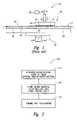
- FIG. 1schematically illustrates a rotary CMP machine 10 with a platen 20 , a head 30 , and a planarizing pad 40 .
- the CMP machine 10may also have a conventional subpad 25 between an upper surface 22 of the platen 20 and a lower surface of the planarizing pad 40 .
- a drive assembly 26rotates the platen 20 (indicated by arrow F) and/or reciprocates the platen 20 back and forth (indicated by arrow G). Since the planarizing pad 40 is attached to the subpad 25 , the planarizing pad 40 moves with the platen 20 during planarization.
- the head 30has a lower surface 32 to which a microfeature workpiece 12 may be attached, or the workpiece 12 may be attached to a resilient pad 34 in the head 30 .
- the head 30may be a weighted, free-floating wafer carrier, or the head 30 may be attached to an actuator assembly 36 (shown schematically) to impart rotational motion to the workpiece 12 (indicated by arrow J) and/or reciprocate the workpiece 12 back and forth (indicated by arrow I).
- the planarizing pad 40 and a planarizing solution 44define a planarizing medium that mechanically and/or chemically-mechanically removes material from the surface of the workpiece 12 .
- the planarizing solution 44may be a conventional CMP slurry with abrasive particles and chemicals that etch and/or oxidize the surface of the microfeature workpiece 12 , or the planarizing solution 44 may be a “clean” non-abrasive planarizing solution without abrasive particles. In most CMP applications, abrasive slurries with abrasive particles are used on non-abrasive polishing pads, and clean non-abrasive solutions without abrasive particles are used on fixed-abrasive polishing pads.
- the head 30presses the workpiece 12 face-down against the planarizing pad 40 . More specifically, the head 30 generally presses the microfeature workpiece 12 against a planarizing surface 42 of the planarizing pad 40 in the presence of the planarizing solution 44 , and the platen 20 and/or the head 30 moves to rub the workpiece 12 against the planarizing surface 42 .
- the mechanical and geometric properties of the subpad 25 and the planarizing pad 40are variables that can affect the uniformity of the planarized surfaces and the polishing rate of the process. For example, grooves or other features on the planarizing pad 40 will affect the distribution of planarizing solution under the workpieces, and the hardness of the planarizing pad 40 will affect the polishing rate and the local conformity of the planarizing surface 42 to the contour of the workpiece 12 . Similarly, the hardness and elasticity of the subpad 25 will affect the global compliance of the polishing pad 40 to the workpiece. As such, it is desirable to control the properties of the subpad 25 and the polishing pad 40 .
- One type of existing subpadhas a polymeric matrix and a filler material in the matrix.
- the filler materialcan be polymer spheres, or the filler material can be silica particles, alumina particles, other metal oxide particles, or other inorganic particles that fill spaces within the polymeric matrix.
- the filler materialsare generally used to reduce the manufacturing cost.
- Conventional subpadsoften have a polymeric matrix without a filler material.
- Conventional subpads and existing subpadsmay not perform well for sufficient periods of time.
- subpads with filler materialsmay not have the optimal mechanical properties. More specifically, many desirable filler materials may not be suitably compatible with the polymeric matrix materials. The lack of compatibility between filler materials and polymeric materials can limit the mechanical properties of the subpads. As a result, subpads with filler materials may not perform at optimal levels. Therefore, it would be desirable to enhance the performance of subpads with filler materials.
- FIG. 1is a schematic side elevation view of a CMP machine in accordance with the prior art.
- FIG. 2is a flow chart of a method for manufacturing a CMP subpad in accordance with an embodiment of the invention.
- FIG. 3is a schematic cross-sectional view of a pad assembly for use in a CMP process in accordance with an embodiment of the invention.
- FIG. 4is a schematic side elevation view of a portion of a CMP apparatus using a pad assembly in accordance with an embodiment of the invention.
- the present inventionis directed toward methods and apparatus for mechanically and/or chemically-mechanically removing material from microfeature workpieces.
- Several embodiments of the inventionare directed toward subpads that inhibit or otherwise prevent absorption of liquid.
- Certain subpads in accordance with the inventionare at least generally impermeable to the liquids used in the processing solutions.
- several embodiments of subpads in accordance with the inventionare expected to provide consistent mechanical properties to uniformly planarize the surface of a workpiece and to increase the life of the pad assembly.
- One aspect of the inventionis directed toward subpads for use in removing material from a microfeature workpiece.
- An embodiment of such a subpad in accordance with the inventioncomprises a matrix having a first surface configured to support a polishing medium and a second surface opposite the first surface.
- the subpad in this embodimentfurther includes a hydro-control agent in the matrix.
- the hydro-control agenthas a hydrophobicity that inhibits liquid from absorbing into the subpad.
- the hydro-control agentfor example, can be coupling agents that are generally hydrophobic, surfactants that are hydrophobic, or other agents that are compatible with the matrix and at least generally hydrophobic.
- a subpad in accordance with the inventioncomprises a polymeric medium having a first surface configured to support a polishing pad and a second surface opposite the first surface.
- the subpadcan further include an inorganic filler material in the polymeric medium, and a hydro-agent attached to the inorganic filler material.
- the hydro-agent in this embodimentreduces the permeability of the polymeric medium to liquids.
- Still another embodiment of a subpad in accordance with the inventioncomprises a polymeric material having a first surface configured to support a polishing pad and a second surface opposite the first surface.
- This subpadcan further include an inorganic filler material in the polymeric material and a silane coupling agent attached to the inorganic filler material and/or the polymeric material.
- An embodiment of one such pad assemblycomprises a planarizing medium having a bearing surface configured to contact a workpiece and a backside.
- the pad assemblycan further include a subpad in contact with the backside of the planarizing medium.
- the subpadcomprises a matrix and a hydro-control agent in the matrix, and the hydro-control agent has a hydrophobicity that inhibits liquid from absorbing into the subpad.
- a pad assembly in accordance with the inventioncomprises a planarizing medium having a bearing surface configured to contact the workpiece and a backside.
- This pad assemblyalso includes a subpad in contact with the backside of the planarizing medium.
- the subpadcomprises a polymeric medium, an inorganic filler material in the polymeric medium, and a hydro-agent attached to the inorganic filler material and/or the polymeric medium. The hydro-agent reduces the permeability of the polymeric medium to liquid.
- Still another embodiment of a pad assembly in accordance with the inventioncomprises a planarizing medium having a bearing surface configured to contact the workpiece and a backside, and a subpad in contact with the backside of the planarizing medium.
- the subpad in this embodimentcomprises a polymeric medium, an inorganic filler material in the polymeric medium, and a silane coupling agent attached to the inorganic filler material and/or the polymeric medium.
- An embodiment of one such apparatusincludes a support, a pad assembly on the support, and a workpiece holder configured to hold a workpiece relative to the pad assembly.
- the pad assemblyincludes a planarizing medium and a subpad having a matrix and a hydro-control agent in the matrix.
- the hydro-control agentfor example, has a hydrophobicity that inhibits liquid from absorbing into the subpad.
- the workpiece holder and/or the supportmove to rub the workpiece against the bearing surface of the planarizing medium.
- Another aspect of the inventionis directed toward a method for removing material from a microfeature workpiece.
- One embodiment of such a methodincludes rubbing the workpiece against a pad assembly having a planarizing medium and a subpad under the planarizing medium. This method further includes repelling liquid from the subpad to inhibit liquid from absorbing into the subpad.
- Another aspect of the inventionis directed toward manufacturing subpads for use in removing material from a microfeature workpiece.
- One embodiment of such a methodcomprises attaching a hydro-control agent to an inorganic filler material to increase the hydrophobicity of the inorganic filler material.
- This methodfurther includes mixing a matrix material with the inorganic filler material having the attached hydro-control agent to form a pad mixture, and forming the pad mixture into a subpad.
- FIGS. 2-4illustrate several methods and apparatus for mechanically and/or chemically-mechanically removing material from microfeature workpieces in accordance with embodiments of the invention.
- FIGS. 2-4illustrate several specific details of the invention are set forth in the following description and in FIGS. 2-4 to provide a thorough understanding of certain embodiments of the invention.
- the term “microfeature workpiece”is used throughout to include substrates upon which and/or in which microelectronic devices, micromechanical devices, data storage elements, micro-optics, and other features are fabricated.
- microfeature workpiecescan be semiconductor wafers, glass substrates, dielectric substrates, or many other types of substrates.
- Microfeature workpiecesgenerally have at least several features with critical dimensions less than or equal to 1 ⁇ m, and in many applications the critical dimensions of the smaller features on microfeature workpieces are less than 0.25 ⁇ m or even less than 0.1 ⁇ m.
- planarization and planarizingmean forming a planar surface, forming a smooth surface (e.g., “polishing”), or otherwise removing materials from workpieces. Where the context permits, singular or plural terms may also include the plural or singular term, respectively.
- FIG. 2is a flow chart illustrating a method 100 for manufacturing a CMP subpad used to mechanically remove material from a microfeature workpiece in CMP processing.
- the method 100includes a preparation stage 110 , a mixing stage 120 , and a forming stage 130 .
- the preparation stage 110includes attaching a hydro-control agent to a filler material and/or a matrix material.
- the hydro-control agentcan be chemically grafted to or physically adsorbed with the filler material.
- the hydro-control agentcan be chemically anchored through graft polymerizations, such as free radicals.
- the mixing stage 120includes mixing a matrix material, the filler material, and the hydro-control agent to form a pad mixture.
- the mixing stage 120can be similar to mixing conventional filler materials with matrix materials known in the art of manufacturing CMP subpads.
- the forming stage 130can include casting, molding, extrusion, photo-imaging, printing, sintering, coating, or other techniques.
- the forming stagecan include transferring the pad mixture to a mold and curing the pad mixture for a suitable period. The mixture is then cooled to form a molded article including the matrix material, the filler material, and the hydro-control agent. The molded article can then be “skived” into thin sheets to form a suitable subpad.
- the preparation stage 110can be performed using a number of different matrix materials, filler materials, and hydro-control agents.
- the matrix materialscan be polyurethane or other suitable polymeric materials.
- the filler materialcan include silica particles, alumina particles, other metal oxide particles, and other types of inorganic particles.
- the filler materialsare not limited to including inorganic particles, but rather the filler material can be polymeric microballoons.
- the hydro-control agentscan include coupling agents and/or surfactants.
- suitable coupling agentsare silanes, such as fluoroalkyltrichlorosilane, or other compounds of silicon and hydrogen (Si n H 2n+2 ).
- the silane coupling agentscan also be N-(2-amino-ethyl)-3-aminopropyl-trimethoxysilane (Z-2020), N-(2-(vinylbenzyl-amino)-ethyl)-3-amino-propyl-trimethoxysilane (Z-6032), or 3-glycidoxy-propyl-trimethoxysilane (Z-6040).
- Silane coupling agentsadhere to inorganic filler materials and the polymeric material because the Si(OR 3 ) portion reacts with the inorganic materials and the organofunctional group reacts with the polymeric materials.
- the silane coupling agentmay be applied to the inorganic filler materials as a pretreatment before being added to the matrix material, or the coupling agent may be applied directly to the matrix material.
- the silane coupling agentis attached to the filler material by adsorbing the coupling agent to the surface of the inorganic particles of the filler material. This process, more specifically, can include adsorbing the silane coupling agent to the inorganic particles out of a solution containing the silane coupling agent.
- the hydro-control elementscan potentially be surfactants that are typically physically adsorbed to the inorganic filler materials.
- Typical surfactantsare water-soluble, surface-active agents that include a hydrophobic portion, such as a long alkyl chain.
- the surfactantscan be adsorbed or otherwise attached to the filler material, or the surfactants can be mixed with the polymeric matrix material.
- the hydro-control agent for use in the preparation stage 110is typically selected to increase the hydrophobicity of the filler material.
- the hydrophobic nature of the hydro-control agentis at least partially imparted to the pad mixture.
- the individual subpads formed from the pad mixtureaccordingly have a higher hydrophobicity compared to subpads formed of the same matrix material and filler material without the hydro-control agent.
- FIG. 3is a schematic cross-sectional view of a subpad 200 in accordance with one embodiment of the invention.
- the subpad 200includes a planarizing medium 210 (e.g., a planarizing pad) having a bearing surface 212 and a backside 214 .
- the bearing surface 212is configured to contact the surface of a microfeature workpiece to mechanically and/or chemically-mechanically remove material from the workpiece.
- the planarizing medium 210can have grooves, raised features (e.g., truncated cones or pyramids), or other structures that promote or otherwise control the distribution of planarizing solution.
- the planarizing medium 210can include abrasive particles fixed at the bearing surface 212 , or in other embodiments the planarizing medium does not include fixed-abrasive particles.
- the pad assembly 200further includes a subpad 220 attached to the backside 214 of the planarizing medium 210 .
- the subpad 220includes a matrix 222 and an enhanced filler material 230 .
- the matrix 222can be a polymeric material, such as polyurethane or other suitable polymers.
- the enhanced filler material 230can include a filler element 232 and a hydro-control agent 234 attached to the filler element 232 .
- the filler element 232can be an inorganic particle or another type of particle
- the hydro-control agent 234can be a compound that increases the hydrophobicity of the matrix 222 and/or the filler element 232 .
- the hydro-control agentcan accordingly be any of the coupling agents and/or surfactants set forth above.
- the enhanced filler material 230imparts a high hydrophobicity to the subpad 220 that inhibits or otherwise prevents liquids from absorbing into the matrix 222 .
- the subpadis expected to be at least substantially impermeable to liquids.
- the subpad 220is expected to have consistent mechanical properties for a long period of time because the liquids in the planarizing solution are not likely to affect the size, compressability, and/or elasticity of the matrix material 222 as much as subpads without the hydro-control agent 234 .
- the subpad 220therefore, is expected to provide good uniformity and have a long operating life.
- FIG. 4is a schematic view of a machine 300 that uses an embodiment of the pad assembly 200 set forth above with respect to FIG. 3 .
- the machine 300includes a support 320 , a workpiece holder or head 330 , and the pad assembly 200 .
- the head 330has a lower surface 332 in a retaining cavity and a resilient pad 334 in the retaining cavity.
- the microfeature workpiece 12can be attached to the resilient pad 334 or directly to the lower surface 332 of the head 330 .
- the machine 300further includes a controller 360 for operating the head 330 and/or the support 320 to rub the workpiece 12 against the bearing surface 212 of the planarizing medium 210 .
- a planarizing solution 334can be dispensed onto the bearing surface 212 to remove material from the workpiece 12 .
- the liquids from the planarizing solution 334are inhibited from absorbing into the subpad 220 by the enhanced filler material 230 .
Landscapes
- Engineering & Computer Science (AREA)
- Mechanical Engineering (AREA)
- Finish Polishing, Edge Sharpening, And Grinding By Specific Grinding Devices (AREA)
- Mechanical Treatment Of Semiconductor (AREA)
Abstract
Description
- 1) Adsorb or otherwise attach fluoroalkyltrichlorosilane molecules to silica particles.
- 2) Mix the silica particles and the fluoroalkyltrichlorosilane molecules with a polymeric material to form a pad mixture.
- 3) Optionally mold, cast or extrude the pad mixture of the polymeric material, silica particles, and fluoroalkyltrichlorosilane molecules.
- 4) Cure the pad mixture.
- 5) Optionally cut the cured pad mixture into subpads.
- 1) Adsorb or otherwise attach fluoroalkyltrichlorosilane molecules to alumina particles.
- 2) Mix the alumina particles and the fluoroalkyltrichlorosilane molecules with a polymeric material to form a pad mixture.
- 3) Optionally mold, cast or extrude the pad mixture of the polymeric material, silica particles, and fluoroalkyltrichlorosilane molecules.
- 4) Cure the pad mixture.
- 5) Optionally cut the cured pad mixture into subpads.
- 1) Mix fluoroalkyltrichlorosilane with a polymeric material.
- 2) Add silica particles to the mixture of fluoroalkyltrichlorosilane and polymeric material to form a pad mixture.
- 3) Optionally mold, cast or extrude the pad mixture.
- 4) Cure the pad mixture.
- 5) Optionally cut the pad mixture into subpads.
- 1) Mix fluoroalkyltrichlorosilane with a polymeric material.
- 2) Add alumina particles to the mixture of fluoroalkyltrichlorosilane and polymeric material to form a pad mixture.
- 3) Optionally mold, cast or extrude the pad mixture.
- 4) Cure the pad mixture.
- 5) Optionally cut the pad mixture into subpads.
C. Embodiments of Apparatus and Methods for Removing Material
Claims (48)
Priority Applications (3)
| Application Number | Priority Date | Filing Date | Title |
|---|---|---|---|
| US11/218,239US7294049B2 (en) | 2005-09-01 | 2005-09-01 | Method and apparatus for removing material from microfeature workpieces |
| US11/938,097US7628680B2 (en) | 2005-09-01 | 2007-11-09 | Method and apparatus for removing material from microfeature workpieces |
| US12/621,366US8105131B2 (en) | 2005-09-01 | 2009-11-18 | Method and apparatus for removing material from microfeature workpieces |
Applications Claiming Priority (1)
| Application Number | Priority Date | Filing Date | Title |
|---|---|---|---|
| US11/218,239US7294049B2 (en) | 2005-09-01 | 2005-09-01 | Method and apparatus for removing material from microfeature workpieces |
Related Child Applications (1)
| Application Number | Title | Priority Date | Filing Date |
|---|---|---|---|
| US11/938,097DivisionUS7628680B2 (en) | 2005-09-01 | 2007-11-09 | Method and apparatus for removing material from microfeature workpieces |
Publications (2)
| Publication Number | Publication Date |
|---|---|
| US20070049177A1 US20070049177A1 (en) | 2007-03-01 |
| US7294049B2true US7294049B2 (en) | 2007-11-13 |
Family
ID=37804921
Family Applications (3)
| Application Number | Title | Priority Date | Filing Date |
|---|---|---|---|
| US11/218,239Expired - LifetimeUS7294049B2 (en) | 2005-09-01 | 2005-09-01 | Method and apparatus for removing material from microfeature workpieces |
| US11/938,097Expired - Fee RelatedUS7628680B2 (en) | 2005-09-01 | 2007-11-09 | Method and apparatus for removing material from microfeature workpieces |
| US12/621,366Active2026-05-13US8105131B2 (en) | 2005-09-01 | 2009-11-18 | Method and apparatus for removing material from microfeature workpieces |
Family Applications After (2)
| Application Number | Title | Priority Date | Filing Date |
|---|---|---|---|
| US11/938,097Expired - Fee RelatedUS7628680B2 (en) | 2005-09-01 | 2007-11-09 | Method and apparatus for removing material from microfeature workpieces |
| US12/621,366Active2026-05-13US8105131B2 (en) | 2005-09-01 | 2009-11-18 | Method and apparatus for removing material from microfeature workpieces |
Country Status (1)
| Country | Link |
|---|---|
| US (3) | US7294049B2 (en) |
Cited By (2)
| Publication number | Priority date | Publication date | Assignee | Title |
|---|---|---|---|---|
| US7628680B2 (en)* | 2005-09-01 | 2009-12-08 | Micron Technology, Inc. | Method and apparatus for removing material from microfeature workpieces |
| US20140364041A1 (en)* | 2011-12-16 | 2014-12-11 | Lg Siltron Inc. | Apparatus and method for polishing wafer |
Families Citing this family (3)
| Publication number | Priority date | Publication date | Assignee | Title |
|---|---|---|---|---|
| US8801497B2 (en)* | 2009-04-30 | 2014-08-12 | Rdc Holdings, Llc | Array of abrasive members with resilient support |
| CN103153538B (en)* | 2010-10-15 | 2016-06-01 | 3M创新有限公司 | Abrasive product |
| US20150044783A1 (en)* | 2013-08-12 | 2015-02-12 | Micron Technology, Inc. | Methods of alleviating adverse stress effects on a wafer, and methods of forming a semiconductor device |
Citations (121)
| Publication number | Priority date | Publication date | Assignee | Title |
|---|---|---|---|---|
| US5020283A (en) | 1990-01-22 | 1991-06-04 | Micron Technology, Inc. | Polishing pad with uniform abrasion |
| US5081796A (en) | 1990-08-06 | 1992-01-21 | Micron Technology, Inc. | Method and apparatus for mechanical planarization and endpoint detection of a semiconductor wafer |
| US5177908A (en) | 1990-01-22 | 1993-01-12 | Micron Technology, Inc. | Polishing pad |
| US5232875A (en) | 1992-10-15 | 1993-08-03 | Micron Technology, Inc. | Method and apparatus for improving planarity of chemical-mechanical planarization operations |
| US5234867A (en) | 1992-05-27 | 1993-08-10 | Micron Technology, Inc. | Method for planarizing semiconductor wafers with a non-circular polishing pad |
| US5240552A (en) | 1991-12-11 | 1993-08-31 | Micron Technology, Inc. | Chemical mechanical planarization (CMP) of a semiconductor wafer using acoustical waves for in-situ end point detection |
| US5244534A (en) | 1992-01-24 | 1993-09-14 | Micron Technology, Inc. | Two-step chemical mechanical polishing process for producing flush and protruding tungsten plugs |
| US5245796A (en) | 1992-04-02 | 1993-09-21 | At&T Bell Laboratories | Slurry polisher using ultrasonic agitation |
| US5245790A (en) | 1992-02-14 | 1993-09-21 | Lsi Logic Corporation | Ultrasonic energy enhanced chemi-mechanical polishing of silicon wafers |
| USRE34425E (en) | 1990-08-06 | 1993-11-02 | Micron Technology, Inc. | Method and apparatus for mechanical planarization and endpoint detection of a semiconductor wafer |
| US5433651A (en) | 1993-12-22 | 1995-07-18 | International Business Machines Corporation | In-situ endpoint detection and process monitoring method and apparatus for chemical-mechanical polishing |
| US5449314A (en) | 1994-04-25 | 1995-09-12 | Micron Technology, Inc. | Method of chimical mechanical polishing for dielectric layers |
| US5486129A (en) | 1993-08-25 | 1996-01-23 | Micron Technology, Inc. | System and method for real-time control of semiconductor a wafer polishing, and a polishing head |
| US5514245A (en) | 1992-01-27 | 1996-05-07 | Micron Technology, Inc. | Method for chemical planarization (CMP) of a semiconductor wafer to provide a planar surface free of microscratches |
| US5533924A (en) | 1994-09-01 | 1996-07-09 | Micron Technology, Inc. | Polishing apparatus, a polishing wafer carrier apparatus, a replacable component for a particular polishing apparatus and a process of polishing wafers |
| US5540810A (en) | 1992-12-11 | 1996-07-30 | Micron Technology Inc. | IC mechanical planarization process incorporating two slurry compositions for faster material removal times |
| US5618381A (en) | 1992-01-24 | 1997-04-08 | Micron Technology, Inc. | Multiple step method of chemical-mechanical polishing which minimizes dishing |
| US5624303A (en) | 1996-01-22 | 1997-04-29 | Micron Technology, Inc. | Polishing pad and a method for making a polishing pad with covalently bonded particles |
| US5643060A (en) | 1993-08-25 | 1997-07-01 | Micron Technology, Inc. | System for real-time control of semiconductor wafer polishing including heater |
| US5650619A (en) | 1995-12-21 | 1997-07-22 | Micron Technology, Inc. | Quality control method for detecting defective polishing pads used in chemical-mechanical planarization of semiconductor wafers |
| US5658190A (en) | 1995-12-15 | 1997-08-19 | Micron Technology, Inc. | Apparatus for separating wafers from polishing pads used in chemical-mechanical planarization of semiconductor wafers |
| US5658183A (en) | 1993-08-25 | 1997-08-19 | Micron Technology, Inc. | System for real-time control of semiconductor wafer polishing including optical monitoring |
| US5679065A (en) | 1996-02-23 | 1997-10-21 | Micron Technology, Inc. | Wafer carrier having carrier ring adapted for uniform chemical-mechanical planarization of semiconductor wafers |
| US5690540A (en) | 1996-02-23 | 1997-11-25 | Micron Technology, Inc. | Spiral grooved polishing pad for chemical-mechanical planarization of semiconductor wafers |
| US5698455A (en) | 1995-02-09 | 1997-12-16 | Micron Technologies, Inc. | Method for predicting process characteristics of polyurethane pads |
| US5702292A (en) | 1996-10-31 | 1997-12-30 | Micron Technology, Inc. | Apparatus and method for loading and unloading substrates to a chemical-mechanical planarization machine |
| US5733176A (en) | 1996-05-24 | 1998-03-31 | Micron Technology, Inc. | Polishing pad and method of use |
| US5736427A (en) | 1996-10-08 | 1998-04-07 | Micron Technology, Inc. | Polishing pad contour indicator for mechanical or chemical-mechanical planarization |
| US5738567A (en) | 1996-08-20 | 1998-04-14 | Micron Technology, Inc. | Polishing pad for chemical-mechanical planarization of a semiconductor wafer |
| US5747386A (en) | 1996-10-03 | 1998-05-05 | Micron Technology, Inc. | Rotary coupling |
| US5792709A (en) | 1995-12-19 | 1998-08-11 | Micron Technology, Inc. | High-speed planarizing apparatus and method for chemical mechanical planarization of semiconductor wafers |
| US5795495A (en) | 1994-04-25 | 1998-08-18 | Micron Technology, Inc. | Method of chemical mechanical polishing for dielectric layers |
| US5795218A (en) | 1996-09-30 | 1998-08-18 | Micron Technology, Inc. | Polishing pad with elongated microcolumns |
| US5807165A (en) | 1997-03-26 | 1998-09-15 | International Business Machines Corporation | Method of electrochemical mechanical planarization |
| US5830806A (en) | 1996-10-18 | 1998-11-03 | Micron Technology, Inc. | Wafer backing member for mechanical and chemical-mechanical planarization of substrates |
| US5851135A (en) | 1993-08-25 | 1998-12-22 | Micron Technology, Inc. | System for real-time control of semiconductor wafer polishing |
| US5868896A (en) | 1996-11-06 | 1999-02-09 | Micron Technology, Inc. | Chemical-mechanical planarization machine and method for uniformly planarizing semiconductor wafers |
| US5871392A (en) | 1996-06-13 | 1999-02-16 | Micron Technology, Inc. | Under-pad for chemical-mechanical planarization of semiconductor wafers |
| US5893754A (en) | 1996-05-21 | 1999-04-13 | Micron Technology, Inc. | Method for chemical-mechanical planarization of stop-on-feature semiconductor wafers |
| US5895550A (en) | 1996-12-16 | 1999-04-20 | Micron Technology, Inc. | Ultrasonic processing of chemical mechanical polishing slurries |
| US5919082A (en) | 1997-08-22 | 1999-07-06 | Micron Technology, Inc. | Fixed abrasive polishing pad |
| US5934980A (en) | 1997-06-09 | 1999-08-10 | Micron Technology, Inc. | Method of chemical mechanical polishing |
| US5938801A (en) | 1997-02-12 | 1999-08-17 | Micron Technology, Inc. | Polishing pad and a method for making a polishing pad with covalently bonded particles |
| US5945347A (en) | 1995-06-02 | 1999-08-31 | Micron Technology, Inc. | Apparatus and method for polishing a semiconductor wafer in an overhanging position |
| US5967030A (en) | 1995-11-17 | 1999-10-19 | Micron Technology, Inc. | Global planarization method and apparatus |
| US5972792A (en) | 1996-10-18 | 1999-10-26 | Micron Technology, Inc. | Method for chemical-mechanical planarization of a substrate on a fixed-abrasive polishing pad |
| US5976000A (en) | 1996-05-28 | 1999-11-02 | Micron Technology, Inc. | Polishing pad with incompressible, highly soluble particles for chemical-mechanical planarization of semiconductor wafers |
| US5990012A (en) | 1998-01-27 | 1999-11-23 | Micron Technology, Inc. | Chemical-mechanical polishing of hydrophobic materials by use of incorporated-particle polishing pads |
| US5997384A (en) | 1997-12-22 | 1999-12-07 | Micron Technology, Inc. | Method and apparatus for controlling planarizing characteristics in mechanical and chemical-mechanical planarization of microelectronic substrates |
| US6036586A (en) | 1998-07-29 | 2000-03-14 | Micron Technology, Inc. | Apparatus and method for reducing removal forces for CMP pads |
| US6039633A (en) | 1998-10-01 | 2000-03-21 | Micron Technology, Inc. | Method and apparatus for mechanical and chemical-mechanical planarization of microelectronic-device substrate assemblies |
| US6062958A (en) | 1997-04-04 | 2000-05-16 | Micron Technology, Inc. | Variable abrasive polishing pad for mechanical and chemical-mechanical planarization |
| US6066030A (en) | 1999-03-04 | 2000-05-23 | International Business Machines Corporation | Electroetch and chemical mechanical polishing equipment |
| US6074286A (en) | 1998-01-05 | 2000-06-13 | Micron Technology, Inc. | Wafer processing apparatus and method of processing a wafer utilizing a processing slurry |
| US6083085A (en) | 1997-12-22 | 2000-07-04 | Micron Technology, Inc. | Method and apparatus for planarizing microelectronic substrates and conditioning planarizing media |
| US6090475A (en) | 1996-05-24 | 2000-07-18 | Micron Technology Inc. | Polishing pad, methods of manufacturing and use |
| US6110820A (en) | 1995-06-07 | 2000-08-29 | Micron Technology, Inc. | Low scratch density chemical mechanical planarization process |
| US6125255A (en) | 1996-09-23 | 2000-09-26 | Xerox Corporation | Magnet assembly with inserts and method of manufacturing |
| US6135856A (en) | 1996-01-19 | 2000-10-24 | Micron Technology, Inc. | Apparatus and method for semiconductor planarization |
| US6139402A (en) | 1997-12-30 | 2000-10-31 | Micron Technology, Inc. | Method and apparatus for mechanical and chemical-mechanical planarization of microelectronic substrates |
| US6143155A (en) | 1998-06-11 | 2000-11-07 | Speedfam Ipec Corp. | Method for simultaneous non-contact electrochemical plating and planarizing of semiconductor wafers using a bipiolar electrode assembly |
| US6152808A (en) | 1998-08-25 | 2000-11-28 | Micron Technology, Inc. | Microelectronic substrate polishing systems, semiconductor wafer polishing systems, methods of polishing microelectronic substrates, and methods of polishing wafers |
| US6176763B1 (en) | 1999-02-04 | 2001-01-23 | Micron Technology, Inc. | Method and apparatus for uniformly planarizing a microelectronic substrate |
| US6176992B1 (en) | 1998-11-03 | 2001-01-23 | Nutool, Inc. | Method and apparatus for electro-chemical mechanical deposition |
| US6187681B1 (en) | 1998-10-14 | 2001-02-13 | Micron Technology, Inc. | Method and apparatus for planarization of a substrate |
| US6191037B1 (en) | 1998-09-03 | 2001-02-20 | Micron Technology, Inc. | Methods, apparatuses and substrate assembly structures for fabricating microelectronic components using mechanical and chemical-mechanical planarization processes |
| US6193588B1 (en) | 1998-09-02 | 2001-02-27 | Micron Technology, Inc. | Method and apparatus for planarizing and cleaning microelectronic substrates |
| US6196899B1 (en) | 1999-06-21 | 2001-03-06 | Micron Technology, Inc. | Polishing apparatus |
| US6200901B1 (en) | 1998-06-10 | 2001-03-13 | Micron Technology, Inc. | Polishing polymer surfaces on non-porous CMP pads |
| US6203404B1 (en) | 1999-06-03 | 2001-03-20 | Micron Technology, Inc. | Chemical mechanical polishing methods |
| US6203413B1 (en) | 1999-01-13 | 2001-03-20 | Micron Technology, Inc. | Apparatus and methods for conditioning polishing pads in mechanical and/or chemical-mechanical planarization of microelectronic-device substrate assemblies |
| US6203407B1 (en) | 1998-09-03 | 2001-03-20 | Micron Technology, Inc. | Method and apparatus for increasing-chemical-polishing selectivity |
| US6206759B1 (en) | 1998-11-30 | 2001-03-27 | Micron Technology, Inc. | Polishing pads and planarizing machines for mechanical or chemical-mechanical planarization of microelectronic-device substrate assemblies, and methods for making and using such pads and machines |
| US6206754B1 (en) | 1999-08-31 | 2001-03-27 | Micron Technology, Inc. | Endpoint detection apparatus, planarizing machines with endpointing apparatus, and endpointing methods for mechanical or chemical-mechanical planarization of microelectronic substrate assemblies |
| US6206756B1 (en) | 1998-11-10 | 2001-03-27 | Micron Technology, Inc. | Tungsten chemical-mechanical polishing process using a fixed abrasive polishing pad and a tungsten layer chemical-mechanical polishing solution specifically adapted for chemical-mechanical polishing with a fixed abrasive pad |
| US6210257B1 (en) | 1998-05-29 | 2001-04-03 | Micron Technology, Inc. | Web-format polishing pads and methods for manufacturing and using web-format polishing pads in mechanical and chemical-mechanical planarization of microelectronic substrates |
| US6213845B1 (en) | 1999-04-26 | 2001-04-10 | Micron Technology, Inc. | Apparatus for in-situ optical endpointing on web-format planarizing machines in mechanical or chemical-mechanical planarization of microelectronic-device substrate assemblies and methods for making and using same |
| US6218316B1 (en) | 1998-10-22 | 2001-04-17 | Micron Technology, Inc. | Planarization of non-planar surfaces in device fabrication |
| US6220934B1 (en) | 1998-07-23 | 2001-04-24 | Micron Technology, Inc. | Method for controlling pH during planarization and cleaning of microelectronic substrates |
| US6227955B1 (en) | 1999-04-20 | 2001-05-08 | Micron Technology, Inc. | Carrier heads, planarizing machines and methods for mechanical or chemical-mechanical planarization of microelectronic-device substrate assemblies |
| US6238273B1 (en) | 1999-08-31 | 2001-05-29 | Micron Technology, Inc. | Methods for predicting polishing parameters of polishing pads and methods and machines for planarizing microelectronic substrate assemblies in mechanical or chemical-mechanical planarization |
| US6244944B1 (en) | 1999-08-31 | 2001-06-12 | Micron Technology, Inc. | Method and apparatus for supporting and cleaning a polishing pad for chemical-mechanical planarization of microelectronic substrates |
| US6250994B1 (en) | 1998-10-01 | 2001-06-26 | Micron Technology, Inc. | Methods and apparatuses for mechanical and chemical-mechanical planarization of microelectronic-device substrate assemblies on planarizing pads |
| US6261163B1 (en) | 1999-08-30 | 2001-07-17 | Micron Technology, Inc. | Web-format planarizing machines and methods for planarizing microelectronic substrate assemblies |
| US6267650B1 (en) | 1999-08-09 | 2001-07-31 | Micron Technology, Inc. | Apparatus and methods for substantial planarization of solder bumps |
| US6273800B1 (en) | 1999-08-31 | 2001-08-14 | Micron Technology, Inc. | Method and apparatus for supporting a polishing pad during chemical-mechanical planarization of microelectronic substrates |
| US6273796B1 (en) | 1999-09-01 | 2001-08-14 | Micron Technology, Inc. | Method and apparatus for planarizing a microelectronic substrate with a tilted planarizing surface |
| US6276996B1 (en) | 1998-11-10 | 2001-08-21 | Micron Technology, Inc. | Copper chemical-mechanical polishing process using a fixed abrasive polishing pad and a copper layer chemical-mechanical polishing solution specifically adapted for chemical-mechanical polishing with a fixed abrasive pad |
| US6296557B1 (en) | 1999-04-02 | 2001-10-02 | Micron Technology, Inc. | Method and apparatus for releasably attaching polishing pads to planarizing machines in mechanical and/or chemical-mechanical planarization of microelectronic-device substrate assemblies |
| US6306768B1 (en) | 1999-11-17 | 2001-10-23 | Micron Technology, Inc. | Method for planarizing microelectronic substrates having apertures |
| US6306012B1 (en) | 1999-07-20 | 2001-10-23 | Micron Technology, Inc. | Methods and apparatuses for planarizing microelectronic substrate assemblies |
| US6313038B1 (en) | 2000-04-26 | 2001-11-06 | Micron Technology, Inc. | Method and apparatus for controlling chemical interactions during planarization of microelectronic substrates |
| US6328632B1 (en) | 1999-08-31 | 2001-12-11 | Micron Technology, Inc. | Polishing pads and planarizing machines for mechanical and/or chemical-mechanical planarization of microelectronic substrate assemblies |
| US6331488B1 (en) | 1997-05-23 | 2001-12-18 | Micron Technology, Inc. | Planarization process for semiconductor substrates |
| US6331135B1 (en) | 1999-08-31 | 2001-12-18 | Micron Technology, Inc. | Method and apparatus for mechanical and chemical-mechanical planarization of microelectronic substrates with metal compound abrasives |
| US6352466B1 (en) | 1998-08-31 | 2002-03-05 | Micron Technology, Inc. | Method and apparatus for wireless transfer of chemical-mechanical planarization measurements |
| US6358129B2 (en) | 1998-11-11 | 2002-03-19 | Micron Technology, Inc. | Backing members and planarizing machines for mechanical and chemical-mechanical planarization of microelectronic-device substrate assemblies, and methods of making and using such backing members |
| US6364749B1 (en) | 1999-09-02 | 2002-04-02 | Micron Technology, Inc. | CMP polishing pad with hydrophilic surfaces for enhanced wetting |
| US6368190B1 (en) | 2000-01-26 | 2002-04-09 | Agere Systems Guardian Corp. | Electrochemical mechanical planarization apparatus and method |
| US6376381B1 (en) | 1999-08-31 | 2002-04-23 | Micron Technology, Inc. | Planarizing solutions, planarizing machines, and methods for mechanical and/or chemical-mechanical planarization of microelectronic substrate assemblies |
| US6383934B1 (en) | 1999-09-02 | 2002-05-07 | Micron Technology, Inc. | Method and apparatus for chemical-mechanical planarization of microelectronic substrates with selected planarizing liquids |
| US6387289B1 (en) | 2000-05-04 | 2002-05-14 | Micron Technology, Inc. | Planarizing machines and methods for mechanical and/or chemical-mechanical planarization of microelectronic-device substrate assemblies |
| US6395620B1 (en) | 1996-10-08 | 2002-05-28 | Micron Technology, Inc. | Method for forming a planar surface over low density field areas on a semiconductor wafer |
| US6402884B1 (en) | 1999-04-09 | 2002-06-11 | Micron Technology, Inc. | Planarizing solutions, planarizing machines and methods for mechanical or chemical-mechanical planarization of microelectronic-device substrate assemblies |
| US6428586B1 (en) | 1999-12-14 | 2002-08-06 | Rodel Holdings Inc. | Method of manufacturing a polymer or polymer/composite polishing pad |
| US6428386B1 (en) | 2000-06-16 | 2002-08-06 | Micron Technology, Inc. | Planarizing pads, planarizing machines, and methods for mechanical and/or chemical-mechanical planarization of microelectronic-device substrate assemblies |
| US6447369B1 (en) | 2000-08-30 | 2002-09-10 | Micron Technology, Inc. | Planarizing machines and alignment systems for mechanical and/or chemical-mechanical planarization of microelectronic substrates |
| US6454634B1 (en) | 2000-05-27 | 2002-09-24 | Rodel Holdings Inc. | Polishing pads for chemical mechanical planarization |
| US6498101B1 (en) | 2000-02-28 | 2002-12-24 | Micron Technology, Inc. | Planarizing pads, planarizing machines and methods for making and using planarizing pads in mechanical and chemical-mechanical planarization of microelectronic device substrate assemblies |
| US6520834B1 (en) | 2000-08-09 | 2003-02-18 | Micron Technology, Inc. | Methods and apparatuses for analyzing and controlling performance parameters in mechanical and chemical-mechanical planarization of microelectronic substrates |
| US6547640B2 (en) | 2000-03-23 | 2003-04-15 | Micron Technology, Inc. | Devices and methods for in-situ control of mechanical or chemical-mechanical planarization of microelectronic-device substrate assemblies |
| US6582623B1 (en) | 1999-07-07 | 2003-06-24 | Cabot Microelectronics Corporation | CMP composition containing silane modified abrasive particles |
| US6592443B1 (en) | 2000-08-30 | 2003-07-15 | Micron Technology, Inc. | Method and apparatus for forming and using planarizing pads for mechanical and chemical-mechanical planarization of microelectronic substrates |
| US6609947B1 (en) | 2000-08-30 | 2003-08-26 | Micron Technology, Inc. | Planarizing machines and control systems for mechanical and/or chemical-mechanical planarization of micro electronic substrates |
| US6620036B2 (en) | 1999-08-31 | 2003-09-16 | Rodel Holdings, Inc | Stacked polishing pad having sealed edge |
| US6623329B1 (en) | 2000-08-31 | 2003-09-23 | Micron Technology, Inc. | Method and apparatus for supporting a microelectronic substrate relative to a planarization pad |
| US6646348B1 (en) | 2000-07-05 | 2003-11-11 | Cabot Microelectronics Corporation | Silane containing polishing composition for CMP |
| US6652764B1 (en) | 2000-08-31 | 2003-11-25 | Micron Technology, Inc. | Methods and apparatuses for making and using planarizing pads for mechanical and chemical-mechanical planarization of microelectronic substrates |
| US6666749B2 (en) | 2001-08-30 | 2003-12-23 | Micron Technology, Inc. | Apparatus and method for enhanced processing of microelectronic workpieces |
| US20050032464A1 (en)* | 2003-08-07 | 2005-02-10 | Swisher Robert G. | Polishing pad having edge surface treatment |
| US6913517B2 (en) | 2002-05-23 | 2005-07-05 | Cabot Microelectronics Corporation | Microporous polishing pads |
Family Cites Families (6)
| Publication number | Priority date | Publication date | Assignee | Title |
|---|---|---|---|---|
| DE1232959B (en)* | 1964-09-12 | 1967-01-26 | Walter Bloechl | Process for the production of an impregnating agent which can be used from an aqueous solution |
| US6582383B2 (en)* | 1999-08-10 | 2003-06-24 | Larry R. Horning | Bandage for application of therapeutic cold or heat treatments to injuries |
| WO2002049762A2 (en)* | 2000-12-18 | 2002-06-27 | The Regents Of The University Of California | Microchannels for efficient fluid transport |
| US6702292B2 (en)* | 2001-01-18 | 2004-03-09 | Gary S. Takowsky | Game ball system incorporating means for position sensing |
| US20060089094A1 (en)* | 2004-10-27 | 2006-04-27 | Swisher Robert G | Polyurethane urea polishing pad |
| US7294049B2 (en)* | 2005-09-01 | 2007-11-13 | Micron Technology, Inc. | Method and apparatus for removing material from microfeature workpieces |
- 2005
- 2005-09-01USUS11/218,239patent/US7294049B2/ennot_activeExpired - Lifetime
- 2007
- 2007-11-09USUS11/938,097patent/US7628680B2/ennot_activeExpired - Fee Related
- 2009
- 2009-11-18USUS12/621,366patent/US8105131B2/enactiveActive
Patent Citations (178)
| Publication number | Priority date | Publication date | Assignee | Title |
|---|---|---|---|---|
| US5177908A (en) | 1990-01-22 | 1993-01-12 | Micron Technology, Inc. | Polishing pad |
| US5020283A (en) | 1990-01-22 | 1991-06-04 | Micron Technology, Inc. | Polishing pad with uniform abrasion |
| US5421769A (en) | 1990-01-22 | 1995-06-06 | Micron Technology, Inc. | Apparatus for planarizing semiconductor wafers, and a polishing pad for a planarization apparatus |
| US5297364A (en) | 1990-01-22 | 1994-03-29 | Micron Technology, Inc. | Polishing pad with controlled abrasion rate |
| USRE34425E (en) | 1990-08-06 | 1993-11-02 | Micron Technology, Inc. | Method and apparatus for mechanical planarization and endpoint detection of a semiconductor wafer |
| US5081796A (en) | 1990-08-06 | 1992-01-21 | Micron Technology, Inc. | Method and apparatus for mechanical planarization and endpoint detection of a semiconductor wafer |
| US5240552A (en) | 1991-12-11 | 1993-08-31 | Micron Technology, Inc. | Chemical mechanical planarization (CMP) of a semiconductor wafer using acoustical waves for in-situ end point detection |
| US5618381A (en) | 1992-01-24 | 1997-04-08 | Micron Technology, Inc. | Multiple step method of chemical-mechanical polishing which minimizes dishing |
| US5244534A (en) | 1992-01-24 | 1993-09-14 | Micron Technology, Inc. | Two-step chemical mechanical polishing process for producing flush and protruding tungsten plugs |
| US5514245A (en) | 1992-01-27 | 1996-05-07 | Micron Technology, Inc. | Method for chemical planarization (CMP) of a semiconductor wafer to provide a planar surface free of microscratches |
| US5245790A (en) | 1992-02-14 | 1993-09-21 | Lsi Logic Corporation | Ultrasonic energy enhanced chemi-mechanical polishing of silicon wafers |
| US5245796A (en) | 1992-04-02 | 1993-09-21 | At&T Bell Laboratories | Slurry polisher using ultrasonic agitation |
| US5234867A (en) | 1992-05-27 | 1993-08-10 | Micron Technology, Inc. | Method for planarizing semiconductor wafers with a non-circular polishing pad |
| US5232875A (en) | 1992-10-15 | 1993-08-03 | Micron Technology, Inc. | Method and apparatus for improving planarity of chemical-mechanical planarization operations |
| US5540810A (en) | 1992-12-11 | 1996-07-30 | Micron Technology Inc. | IC mechanical planarization process incorporating two slurry compositions for faster material removal times |
| US6040245A (en) | 1992-12-11 | 2000-03-21 | Micron Technology, Inc. | IC mechanical planarization process incorporating two slurry compositions for faster material removal times |
| US5994224A (en) | 1992-12-11 | 1999-11-30 | Micron Technology Inc. | IC mechanical planarization process incorporating two slurry compositions for faster material removal times |
| US5643060A (en) | 1993-08-25 | 1997-07-01 | Micron Technology, Inc. | System for real-time control of semiconductor wafer polishing including heater |
| US5730642A (en) | 1993-08-25 | 1998-03-24 | Micron Technology, Inc. | System for real-time control of semiconductor wafer polishing including optical montoring |
| US5851135A (en) | 1993-08-25 | 1998-12-22 | Micron Technology, Inc. | System for real-time control of semiconductor wafer polishing |
| US5486129A (en) | 1993-08-25 | 1996-01-23 | Micron Technology, Inc. | System and method for real-time control of semiconductor a wafer polishing, and a polishing head |
| US5658183A (en) | 1993-08-25 | 1997-08-19 | Micron Technology, Inc. | System for real-time control of semiconductor wafer polishing including optical monitoring |
| US6261151B1 (en) | 1993-08-25 | 2001-07-17 | Micron Technology, Inc. | System for real-time control of semiconductor wafer polishing |
| US5433651A (en) | 1993-12-22 | 1995-07-18 | International Business Machines Corporation | In-situ endpoint detection and process monitoring method and apparatus for chemical-mechanical polishing |
| US5449314A (en) | 1994-04-25 | 1995-09-12 | Micron Technology, Inc. | Method of chimical mechanical polishing for dielectric layers |
| US5795495A (en) | 1994-04-25 | 1998-08-18 | Micron Technology, Inc. | Method of chemical mechanical polishing for dielectric layers |
| US5664988A (en) | 1994-09-01 | 1997-09-09 | Micron Technology, Inc. | Process of polishing a semiconductor wafer having an orientation edge discontinuity shape |
| US5533924A (en) | 1994-09-01 | 1996-07-09 | Micron Technology, Inc. | Polishing apparatus, a polishing wafer carrier apparatus, a replacable component for a particular polishing apparatus and a process of polishing wafers |
| US5698455A (en) | 1995-02-09 | 1997-12-16 | Micron Technologies, Inc. | Method for predicting process characteristics of polyurethane pads |
| US6114706A (en) | 1995-02-09 | 2000-09-05 | Micron Technology, Inc. | Method and apparatus for predicting process characteristics of polyurethane pads |
| US6251785B1 (en) | 1995-06-02 | 2001-06-26 | Micron Technology, Inc. | Apparatus and method for polishing a semiconductor wafer in an overhanging position |
| US5945347A (en) | 1995-06-02 | 1999-08-31 | Micron Technology, Inc. | Apparatus and method for polishing a semiconductor wafer in an overhanging position |
| US6110820A (en) | 1995-06-07 | 2000-08-29 | Micron Technology, Inc. | Low scratch density chemical mechanical planarization process |
| US6237483B1 (en) | 1995-11-17 | 2001-05-29 | Micron Technology, Inc. | Global planarization method and apparatus |
| US5967030A (en) | 1995-11-17 | 1999-10-19 | Micron Technology, Inc. | Global planarization method and apparatus |
| US5658190A (en) | 1995-12-15 | 1997-08-19 | Micron Technology, Inc. | Apparatus for separating wafers from polishing pads used in chemical-mechanical planarization of semiconductor wafers |
| US5882248A (en) | 1995-12-15 | 1999-03-16 | Micron Technology, Inc. | Apparatus for separating wafers from polishing pads used in chemical-mechanical planarization of semiconductor wafers |
| US5792709A (en) | 1995-12-19 | 1998-08-11 | Micron Technology, Inc. | High-speed planarizing apparatus and method for chemical mechanical planarization of semiconductor wafers |
| US5825028A (en) | 1995-12-21 | 1998-10-20 | Micron Technology, Inc. | Quality control method for detecting defective polishing pads used in planarization of semiconductor wafers |
| US5650619A (en) | 1995-12-21 | 1997-07-22 | Micron Technology, Inc. | Quality control method for detecting defective polishing pads used in chemical-mechanical planarization of semiconductor wafers |
| US6135856A (en) | 1996-01-19 | 2000-10-24 | Micron Technology, Inc. | Apparatus and method for semiconductor planarization |
| US5823855A (en) | 1996-01-22 | 1998-10-20 | Micron Technology, Inc. | Polishing pad and a method for making a polishing pad with covalently bonded particles |
| US5624303A (en) | 1996-01-22 | 1997-04-29 | Micron Technology, Inc. | Polishing pad and a method for making a polishing pad with covalently bonded particles |
| US5879222A (en) | 1996-01-22 | 1999-03-09 | Micron Technology, Inc. | Abrasive polishing pad with covalently bonded abrasive particles |
| US5690540A (en) | 1996-02-23 | 1997-11-25 | Micron Technology, Inc. | Spiral grooved polishing pad for chemical-mechanical planarization of semiconductor wafers |
| US5679065A (en) | 1996-02-23 | 1997-10-21 | Micron Technology, Inc. | Wafer carrier having carrier ring adapted for uniform chemical-mechanical planarization of semiconductor wafers |
| US5981396A (en) | 1996-05-21 | 1999-11-09 | Micron Technology, Inc. | Method for chemical-mechanical planarization of stop-on-feature semiconductor wafers |
| US5893754A (en) | 1996-05-21 | 1999-04-13 | Micron Technology, Inc. | Method for chemical-mechanical planarization of stop-on-feature semiconductor wafers |
| US6136043A (en) | 1996-05-24 | 2000-10-24 | Micron Technology, Inc. | Polishing pad methods of manufacture and use |
| US6090475A (en) | 1996-05-24 | 2000-07-18 | Micron Technology Inc. | Polishing pad, methods of manufacturing and use |
| US5733176A (en) | 1996-05-24 | 1998-03-31 | Micron Technology, Inc. | Polishing pad and method of use |
| US5976000A (en) | 1996-05-28 | 1999-11-02 | Micron Technology, Inc. | Polishing pad with incompressible, highly soluble particles for chemical-mechanical planarization of semiconductor wafers |
| US5871392A (en) | 1996-06-13 | 1999-02-16 | Micron Technology, Inc. | Under-pad for chemical-mechanical planarization of semiconductor wafers |
| US5980363A (en) | 1996-06-13 | 1999-11-09 | Micron Technology, Inc. | Under-pad for chemical-mechanical planarization of semiconductor wafers |
| US5738567A (en) | 1996-08-20 | 1998-04-14 | Micron Technology, Inc. | Polishing pad for chemical-mechanical planarization of a semiconductor wafer |
| US5910043A (en) | 1996-08-20 | 1999-06-08 | Micron Technology, Inc. | Polishing pad for chemical-mechanical planarization of a semiconductor wafer |
| US6125255A (en) | 1996-09-23 | 2000-09-26 | Xerox Corporation | Magnet assembly with inserts and method of manufacturing |
| US5795218A (en) | 1996-09-30 | 1998-08-18 | Micron Technology, Inc. | Polishing pad with elongated microcolumns |
| US5989470A (en) | 1996-09-30 | 1999-11-23 | Micron Technology, Inc. | Method for making polishing pad with elongated microcolumns |
| US5747386A (en) | 1996-10-03 | 1998-05-05 | Micron Technology, Inc. | Rotary coupling |
| US5954912A (en) | 1996-10-03 | 1999-09-21 | Micro Technology, Inc. | Rotary coupling |
| US5736427A (en) | 1996-10-08 | 1998-04-07 | Micron Technology, Inc. | Polishing pad contour indicator for mechanical or chemical-mechanical planarization |
| US6395620B1 (en) | 1996-10-08 | 2002-05-28 | Micron Technology, Inc. | Method for forming a planar surface over low density field areas on a semiconductor wafer |
| US5972792A (en) | 1996-10-18 | 1999-10-26 | Micron Technology, Inc. | Method for chemical-mechanical planarization of a substrate on a fixed-abrasive polishing pad |
| US5830806A (en) | 1996-10-18 | 1998-11-03 | Micron Technology, Inc. | Wafer backing member for mechanical and chemical-mechanical planarization of substrates |
| US5702292A (en) | 1996-10-31 | 1997-12-30 | Micron Technology, Inc. | Apparatus and method for loading and unloading substrates to a chemical-mechanical planarization machine |
| US6054015A (en) | 1996-10-31 | 2000-04-25 | Micron Technology, Inc. | Apparatus for loading and unloading substrates to a chemical-mechanical planarization machine |
| US5868896A (en) | 1996-11-06 | 1999-02-09 | Micron Technology, Inc. | Chemical-mechanical planarization machine and method for uniformly planarizing semiconductor wafers |
| US6143123A (en) | 1996-11-06 | 2000-11-07 | Micron Technology, Inc. | Chemical-mechanical planarization machine and method for uniformly planarizing semiconductor wafers |
| US5895550A (en) | 1996-12-16 | 1999-04-20 | Micron Technology, Inc. | Ultrasonic processing of chemical mechanical polishing slurries |
| US5938801A (en) | 1997-02-12 | 1999-08-17 | Micron Technology, Inc. | Polishing pad and a method for making a polishing pad with covalently bonded particles |
| US5807165A (en) | 1997-03-26 | 1998-09-15 | International Business Machines Corporation | Method of electrochemical mechanical planarization |
| US6186870B1 (en) | 1997-04-04 | 2001-02-13 | Micron Technology, Inc. | Variable abrasive polishing pad for mechanical and chemical-mechanical planarization |
| US6062958A (en) | 1997-04-04 | 2000-05-16 | Micron Technology, Inc. | Variable abrasive polishing pad for mechanical and chemical-mechanical planarization |
| US6309282B1 (en) | 1997-04-04 | 2001-10-30 | Micron Technology, Inc. | Variable abrasive polishing pad for mechanical and chemical-mechanical planarization |
| US6331488B1 (en) | 1997-05-23 | 2001-12-18 | Micron Technology, Inc. | Planarization process for semiconductor substrates |
| US6234877B1 (en) | 1997-06-09 | 2001-05-22 | Micron Technology, Inc. | Method of chemical mechanical polishing |
| US6120354A (en) | 1997-06-09 | 2000-09-19 | Micron Technology, Inc. | Method of chemical mechanical polishing |
| US5934980A (en) | 1997-06-09 | 1999-08-10 | Micron Technology, Inc. | Method of chemical mechanical polishing |
| US6290579B1 (en) | 1997-08-22 | 2001-09-18 | Micron Technology, Inc. | Fixed abrasive polishing pad |
| US6409586B2 (en) | 1997-08-22 | 2002-06-25 | Micron Technology, Inc. | Fixed abrasive polishing pad |
| US6254460B1 (en) | 1997-08-22 | 2001-07-03 | Micron Technology, Inc. | Fixed abrasive polishing pad |
| US5919082A (en) | 1997-08-22 | 1999-07-06 | Micron Technology, Inc. | Fixed abrasive polishing pad |
| US5997384A (en) | 1997-12-22 | 1999-12-07 | Micron Technology, Inc. | Method and apparatus for controlling planarizing characteristics in mechanical and chemical-mechanical planarization of microelectronic substrates |
| US6350691B1 (en) | 1997-12-22 | 2002-02-26 | Micron Technology, Inc. | Method and apparatus for planarizing microelectronic substrates and conditioning planarizing media |
| US6083085A (en) | 1997-12-22 | 2000-07-04 | Micron Technology, Inc. | Method and apparatus for planarizing microelectronic substrates and conditioning planarizing media |
| US6354923B1 (en) | 1997-12-22 | 2002-03-12 | Micron Technology, Inc. | Apparatus for planarizing microelectronic substrates and conditioning planarizing media |
| US6364757B2 (en) | 1997-12-30 | 2002-04-02 | Micron Technology, Inc. | Method and apparatus for mechanical and chemical-mechanical planarization of microelectronic substrates |
| US6139402A (en) | 1997-12-30 | 2000-10-31 | Micron Technology, Inc. | Method and apparatus for mechanical and chemical-mechanical planarization of microelectronic substrates |
| US6354930B1 (en) | 1997-12-30 | 2002-03-12 | Micron Technology, Inc. | Method and apparatus for mechanical and chemical-mechanical planarization of microelectronic substrates |
| US6234874B1 (en) | 1998-01-05 | 2001-05-22 | Micron Technology, Inc. | Wafer processing apparatus |
| US6074286A (en) | 1998-01-05 | 2000-06-13 | Micron Technology, Inc. | Wafer processing apparatus and method of processing a wafer utilizing a processing slurry |
| US6116988A (en) | 1998-01-05 | 2000-09-12 | Micron Technology Inc. | Method of processing a wafer utilizing a processing slurry |
| US6277015B1 (en) | 1998-01-27 | 2001-08-21 | Micron Technology, Inc. | Polishing pad and system |
| US5990012A (en) | 1998-01-27 | 1999-11-23 | Micron Technology, Inc. | Chemical-mechanical polishing of hydrophobic materials by use of incorporated-particle polishing pads |
| US6210257B1 (en) | 1998-05-29 | 2001-04-03 | Micron Technology, Inc. | Web-format polishing pads and methods for manufacturing and using web-format polishing pads in mechanical and chemical-mechanical planarization of microelectronic substrates |
| US6200901B1 (en) | 1998-06-10 | 2001-03-13 | Micron Technology, Inc. | Polishing polymer surfaces on non-porous CMP pads |
| US6143155A (en) | 1998-06-11 | 2000-11-07 | Speedfam Ipec Corp. | Method for simultaneous non-contact electrochemical plating and planarizing of semiconductor wafers using a bipiolar electrode assembly |
| US6368194B1 (en) | 1998-07-23 | 2002-04-09 | Micron Technology, Inc. | Apparatus for controlling PH during planarization and cleaning of microelectronic substrates |
| US6220934B1 (en) | 1998-07-23 | 2001-04-24 | Micron Technology, Inc. | Method for controlling pH during planarization and cleaning of microelectronic substrates |
| US6036586A (en) | 1998-07-29 | 2000-03-14 | Micron Technology, Inc. | Apparatus and method for reducing removal forces for CMP pads |
| US6152808A (en) | 1998-08-25 | 2000-11-28 | Micron Technology, Inc. | Microelectronic substrate polishing systems, semiconductor wafer polishing systems, methods of polishing microelectronic substrates, and methods of polishing wafers |
| US6352466B1 (en) | 1998-08-31 | 2002-03-05 | Micron Technology, Inc. | Method and apparatus for wireless transfer of chemical-mechanical planarization measurements |
| US6358127B1 (en) | 1998-09-02 | 2002-03-19 | Micron Technology, Inc. | Method and apparatus for planarizing and cleaning microelectronic substrates |
| US6193588B1 (en) | 1998-09-02 | 2001-02-27 | Micron Technology, Inc. | Method and apparatus for planarizing and cleaning microelectronic substrates |
| US6368193B1 (en) | 1998-09-02 | 2002-04-09 | Micron Technology, Inc. | Method and apparatus for planarizing and cleaning microelectronic substrates |
| US6191037B1 (en) | 1998-09-03 | 2001-02-20 | Micron Technology, Inc. | Methods, apparatuses and substrate assembly structures for fabricating microelectronic components using mechanical and chemical-mechanical planarization processes |
| US6325702B2 (en) | 1998-09-03 | 2001-12-04 | Micron Technology, Inc. | Method and apparatus for increasing chemical-mechanical-polishing selectivity |
| US6203407B1 (en) | 1998-09-03 | 2001-03-20 | Micron Technology, Inc. | Method and apparatus for increasing-chemical-polishing selectivity |
| US6250994B1 (en) | 1998-10-01 | 2001-06-26 | Micron Technology, Inc. | Methods and apparatuses for mechanical and chemical-mechanical planarization of microelectronic-device substrate assemblies on planarizing pads |
| US6039633A (en) | 1998-10-01 | 2000-03-21 | Micron Technology, Inc. | Method and apparatus for mechanical and chemical-mechanical planarization of microelectronic-device substrate assemblies |
| US6312558B2 (en) | 1998-10-14 | 2001-11-06 | Micron Technology, Inc. | Method and apparatus for planarization of a substrate |
| US6187681B1 (en) | 1998-10-14 | 2001-02-13 | Micron Technology, Inc. | Method and apparatus for planarization of a substrate |
| US6218316B1 (en) | 1998-10-22 | 2001-04-17 | Micron Technology, Inc. | Planarization of non-planar surfaces in device fabrication |
| US6176992B1 (en) | 1998-11-03 | 2001-01-23 | Nutool, Inc. | Method and apparatus for electro-chemical mechanical deposition |
| US6273786B1 (en) | 1998-11-10 | 2001-08-14 | Micron Technology, Inc. | Tungsten chemical-mechanical polishing process using a fixed abrasive polishing pad and a tungsten layer chemical-mechanical polishing solution specifically adapted for chemical-mechanical polishing with a fixed abrasive pad |
| US6206756B1 (en) | 1998-11-10 | 2001-03-27 | Micron Technology, Inc. | Tungsten chemical-mechanical polishing process using a fixed abrasive polishing pad and a tungsten layer chemical-mechanical polishing solution specifically adapted for chemical-mechanical polishing with a fixed abrasive pad |
| US6276996B1 (en) | 1998-11-10 | 2001-08-21 | Micron Technology, Inc. | Copper chemical-mechanical polishing process using a fixed abrasive polishing pad and a copper layer chemical-mechanical polishing solution specifically adapted for chemical-mechanical polishing with a fixed abrasive pad |
| US6358129B2 (en) | 1998-11-11 | 2002-03-19 | Micron Technology, Inc. | Backing members and planarizing machines for mechanical and chemical-mechanical planarization of microelectronic-device substrate assemblies, and methods of making and using such backing members |
| US6361832B1 (en) | 1998-11-30 | 2002-03-26 | Micron Technology, Inc. | Polishing pads and planarizing machines for mechanical or chemical-mechanical planarization of microelectronic-device substrate assemblies, and methods for making and using such pads and machines |
| US6206759B1 (en) | 1998-11-30 | 2001-03-27 | Micron Technology, Inc. | Polishing pads and planarizing machines for mechanical or chemical-mechanical planarization of microelectronic-device substrate assemblies, and methods for making and using such pads and machines |
| US6203413B1 (en) | 1999-01-13 | 2001-03-20 | Micron Technology, Inc. | Apparatus and methods for conditioning polishing pads in mechanical and/or chemical-mechanical planarization of microelectronic-device substrate assemblies |
| US6176763B1 (en) | 1999-02-04 | 2001-01-23 | Micron Technology, Inc. | Method and apparatus for uniformly planarizing a microelectronic substrate |
| US6066030A (en) | 1999-03-04 | 2000-05-23 | International Business Machines Corporation | Electroetch and chemical mechanical polishing equipment |
| US6296557B1 (en) | 1999-04-02 | 2001-10-02 | Micron Technology, Inc. | Method and apparatus for releasably attaching polishing pads to planarizing machines in mechanical and/or chemical-mechanical planarization of microelectronic-device substrate assemblies |
| US6402884B1 (en) | 1999-04-09 | 2002-06-11 | Micron Technology, Inc. | Planarizing solutions, planarizing machines and methods for mechanical or chemical-mechanical planarization of microelectronic-device substrate assemblies |
| US6227955B1 (en) | 1999-04-20 | 2001-05-08 | Micron Technology, Inc. | Carrier heads, planarizing machines and methods for mechanical or chemical-mechanical planarization of microelectronic-device substrate assemblies |
| US6213845B1 (en) | 1999-04-26 | 2001-04-10 | Micron Technology, Inc. | Apparatus for in-situ optical endpointing on web-format planarizing machines in mechanical or chemical-mechanical planarization of microelectronic-device substrate assemblies and methods for making and using same |
| US6203404B1 (en) | 1999-06-03 | 2001-03-20 | Micron Technology, Inc. | Chemical mechanical polishing methods |
| US6196899B1 (en) | 1999-06-21 | 2001-03-06 | Micron Technology, Inc. | Polishing apparatus |
| US6582623B1 (en) | 1999-07-07 | 2003-06-24 | Cabot Microelectronics Corporation | CMP composition containing silane modified abrasive particles |
| US6306012B1 (en) | 1999-07-20 | 2001-10-23 | Micron Technology, Inc. | Methods and apparatuses for planarizing microelectronic substrate assemblies |
| US6267650B1 (en) | 1999-08-09 | 2001-07-31 | Micron Technology, Inc. | Apparatus and methods for substantial planarization of solder bumps |
| US6306014B1 (en) | 1999-08-30 | 2001-10-23 | Micron Technology, Inc. | Web-format planarizing machines and methods for planarizing microelectronic substrate assemblies |
| US6261163B1 (en) | 1999-08-30 | 2001-07-17 | Micron Technology, Inc. | Web-format planarizing machines and methods for planarizing microelectronic substrate assemblies |
| US6358122B1 (en) | 1999-08-31 | 2002-03-19 | Micron Technology, Inc. | Method and apparatus for mechanical and chemical-mechanical planarization of microelectronic substrates with metal compound abrasives |
| US6368197B2 (en) | 1999-08-31 | 2002-04-09 | Micron Technology, Inc. | Method and apparatus for supporting and cleaning a polishing pad for chemical-mechanical planarization of microelectronic substrates |
| US6350180B2 (en) | 1999-08-31 | 2002-02-26 | Micron Technology, Inc. | Methods for predicting polishing parameters of polishing pads, and methods and machines for planarizing microelectronic substrate assemblies in mechanical or chemical-mechanical planarization |
| US6331135B1 (en) | 1999-08-31 | 2001-12-18 | Micron Technology, Inc. | Method and apparatus for mechanical and chemical-mechanical planarization of microelectronic substrates with metal compound abrasives |
| US6331139B2 (en) | 1999-08-31 | 2001-12-18 | Micron Technology, Inc. | Method and apparatus for supporting a polishing pad during chemical-mechanical planarization of microelectronic substrates |
| US6244944B1 (en) | 1999-08-31 | 2001-06-12 | Micron Technology, Inc. | Method and apparatus for supporting and cleaning a polishing pad for chemical-mechanical planarization of microelectronic substrates |
| US6206754B1 (en) | 1999-08-31 | 2001-03-27 | Micron Technology, Inc. | Endpoint detection apparatus, planarizing machines with endpointing apparatus, and endpointing methods for mechanical or chemical-mechanical planarization of microelectronic substrate assemblies |
| US6361400B2 (en) | 1999-08-31 | 2002-03-26 | Micron Technology, Inc. | Methods for predicting polishing parameters of polishing pads, and methods and machines for planarizing microelectronic substrate assemblies in mechanical or chemical-mechanical planarization |
| US6361417B2 (en) | 1999-08-31 | 2002-03-26 | Micron Technology, Inc. | Method and apparatus for supporting a polishing pad during chemical-mechanical planarization of microelectronic substrates |
| US6354919B2 (en) | 1999-08-31 | 2002-03-12 | Micron Technology, Inc. | Polishing pads and planarizing machines for mechanical and/or chemical-mechanical planarization of microelectronic substrate assemblies |
| US6328632B1 (en) | 1999-08-31 | 2001-12-11 | Micron Technology, Inc. | Polishing pads and planarizing machines for mechanical and/or chemical-mechanical planarization of microelectronic substrate assemblies |
| US6234878B1 (en) | 1999-08-31 | 2001-05-22 | Micron Technology, Inc. | Endpoint detection apparatus, planarizing machines with endpointing apparatus, and endpointing methods for mechanical or chemical-mechanical planarization of microelectronic substrate assemblies |
| US6620036B2 (en) | 1999-08-31 | 2003-09-16 | Rodel Holdings, Inc | Stacked polishing pad having sealed edge |
| US6238273B1 (en) | 1999-08-31 | 2001-05-29 | Micron Technology, Inc. | Methods for predicting polishing parameters of polishing pads and methods and machines for planarizing microelectronic substrate assemblies in mechanical or chemical-mechanical planarization |
| US6273800B1 (en) | 1999-08-31 | 2001-08-14 | Micron Technology, Inc. | Method and apparatus for supporting a polishing pad during chemical-mechanical planarization of microelectronic substrates |
| US6376381B1 (en) | 1999-08-31 | 2002-04-23 | Micron Technology, Inc. | Planarizing solutions, planarizing machines, and methods for mechanical and/or chemical-mechanical planarization of microelectronic substrate assemblies |
| US6273796B1 (en) | 1999-09-01 | 2001-08-14 | Micron Technology, Inc. | Method and apparatus for planarizing a microelectronic substrate with a tilted planarizing surface |
| US6383934B1 (en) | 1999-09-02 | 2002-05-07 | Micron Technology, Inc. | Method and apparatus for chemical-mechanical planarization of microelectronic substrates with selected planarizing liquids |
| US6533893B2 (en) | 1999-09-02 | 2003-03-18 | Micron Technology, Inc. | Method and apparatus for chemical-mechanical planarization of microelectronic substrates with selected planarizing liquids |
| US6364749B1 (en) | 1999-09-02 | 2002-04-02 | Micron Technology, Inc. | CMP polishing pad with hydrophilic surfaces for enhanced wetting |
| US6306768B1 (en) | 1999-11-17 | 2001-10-23 | Micron Technology, Inc. | Method for planarizing microelectronic substrates having apertures |
| US6511576B2 (en) | 1999-11-17 | 2003-01-28 | Micron Technology, Inc. | System for planarizing microelectronic substrates having apertures |
| US6428586B1 (en) | 1999-12-14 | 2002-08-06 | Rodel Holdings Inc. | Method of manufacturing a polymer or polymer/composite polishing pad |
| US6368190B1 (en) | 2000-01-26 | 2002-04-09 | Agere Systems Guardian Corp. | Electrochemical mechanical planarization apparatus and method |
| US6498101B1 (en) | 2000-02-28 | 2002-12-24 | Micron Technology, Inc. | Planarizing pads, planarizing machines and methods for making and using planarizing pads in mechanical and chemical-mechanical planarization of microelectronic device substrate assemblies |
| US6547640B2 (en) | 2000-03-23 | 2003-04-15 | Micron Technology, Inc. | Devices and methods for in-situ control of mechanical or chemical-mechanical planarization of microelectronic-device substrate assemblies |
| US6548407B1 (en) | 2000-04-26 | 2003-04-15 | Micron Technology, Inc. | Method and apparatus for controlling chemical interactions during planarization of microelectronic substrates |
| US6313038B1 (en) | 2000-04-26 | 2001-11-06 | Micron Technology, Inc. | Method and apparatus for controlling chemical interactions during planarization of microelectronic substrates |
| US6579799B2 (en) | 2000-04-26 | 2003-06-17 | Micron Technology, Inc. | Method and apparatus for controlling chemical interactions during planarization of microelectronic substrates |
| US6387289B1 (en) | 2000-05-04 | 2002-05-14 | Micron Technology, Inc. | Planarizing machines and methods for mechanical and/or chemical-mechanical planarization of microelectronic-device substrate assemblies |
| US6582283B2 (en) | 2000-05-27 | 2003-06-24 | Rodel Holdings, Inc. | Polishing pads for chemical mechanical planarization |
| US6454634B1 (en) | 2000-05-27 | 2002-09-24 | Rodel Holdings Inc. | Polishing pads for chemical mechanical planarization |
| US6428386B1 (en) | 2000-06-16 | 2002-08-06 | Micron Technology, Inc. | Planarizing pads, planarizing machines, and methods for mechanical and/or chemical-mechanical planarization of microelectronic-device substrate assemblies |
| US6646348B1 (en) | 2000-07-05 | 2003-11-11 | Cabot Microelectronics Corporation | Silane containing polishing composition for CMP |
| US6520834B1 (en) | 2000-08-09 | 2003-02-18 | Micron Technology, Inc. | Methods and apparatuses for analyzing and controlling performance parameters in mechanical and chemical-mechanical planarization of microelectronic substrates |
| US6447369B1 (en) | 2000-08-30 | 2002-09-10 | Micron Technology, Inc. | Planarizing machines and alignment systems for mechanical and/or chemical-mechanical planarization of microelectronic substrates |
| US6592443B1 (en) | 2000-08-30 | 2003-07-15 | Micron Technology, Inc. | Method and apparatus for forming and using planarizing pads for mechanical and chemical-mechanical planarization of microelectronic substrates |
| US6609947B1 (en) | 2000-08-30 | 2003-08-26 | Micron Technology, Inc. | Planarizing machines and control systems for mechanical and/or chemical-mechanical planarization of micro electronic substrates |
| US6623329B1 (en) | 2000-08-31 | 2003-09-23 | Micron Technology, Inc. | Method and apparatus for supporting a microelectronic substrate relative to a planarization pad |
| US6652764B1 (en) | 2000-08-31 | 2003-11-25 | Micron Technology, Inc. | Methods and apparatuses for making and using planarizing pads for mechanical and chemical-mechanical planarization of microelectronic substrates |
| US6666749B2 (en) | 2001-08-30 | 2003-12-23 | Micron Technology, Inc. | Apparatus and method for enhanced processing of microelectronic workpieces |
| US6913517B2 (en) | 2002-05-23 | 2005-07-05 | Cabot Microelectronics Corporation | Microporous polishing pads |
| US20050032464A1 (en)* | 2003-08-07 | 2005-02-10 | Swisher Robert G. | Polishing pad having edge surface treatment |
Non-Patent Citations (1)
| Title |
|---|
| Kondo, S. et al., "Abrasive-Free Polishing for Copper Damascene Interconnection," Journal of the Electrochemical Society, vol. 147, No. 10, pp. 3907-3913, 2000. |
Cited By (3)
| Publication number | Priority date | Publication date | Assignee | Title |
|---|---|---|---|---|
| US7628680B2 (en)* | 2005-09-01 | 2009-12-08 | Micron Technology, Inc. | Method and apparatus for removing material from microfeature workpieces |
| US8105131B2 (en) | 2005-09-01 | 2012-01-31 | Micron Technology, Inc. | Method and apparatus for removing material from microfeature workpieces |
| US20140364041A1 (en)* | 2011-12-16 | 2014-12-11 | Lg Siltron Inc. | Apparatus and method for polishing wafer |
Also Published As
| Publication number | Publication date |
|---|---|
| US20080064306A1 (en) | 2008-03-13 |
| US8105131B2 (en) | 2012-01-31 |
| US20100059705A1 (en) | 2010-03-11 |
| US20070049177A1 (en) | 2007-03-01 |
| US7628680B2 (en) | 2009-12-08 |
Similar Documents
| Publication | Publication Date | Title |
|---|---|---|
| JP5336699B2 (en) | Polishing method of crystal material | |
| US6548407B1 (en) | Method and apparatus for controlling chemical interactions during planarization of microelectronic substrates | |
| JP6141359B2 (en) | Polishing pad for chemical mechanical planarization | |
| CN107000170B (en) | UV-hardenable CMP pad and method of making the same | |
| US6857941B2 (en) | Multi-phase polishing pad | |
| US6176763B1 (en) | Method and apparatus for uniformly planarizing a microelectronic substrate | |
| KR20060135014A (en) | Polishing pads and methods for manufacturing same | |
| US20070032172A1 (en) | Polishing liquids for activating and/or conditioning fixed abrasive polishing pads, and associated systems and methods | |
| US20020016139A1 (en) | Polishing tool and manufacturing method therefor | |
| US8105131B2 (en) | Method and apparatus for removing material from microfeature workpieces | |
| TWI846748B (en) | Chemical mechanical polishing pad and polishing method | |
| US6939211B2 (en) | Planarizing solutions including abrasive elements, and methods for manufacturing and using such planarizing solutions | |
| US20020098696A1 (en) | Method and apparatus for chemical-mechanical planarization of microelectronic substrates with selected planarizing liquids | |
| KR20100138736A (en) | Double side polishing processing method of semiconductor wafer | |
| JP2023008827A (en) | CMP polishing pad | |
| JP5385653B2 (en) | Polishing pad and polishing method | |
| TWI842767B (en) | Chemical mechanical polishing pad having a positive zeta potential for polishing a substrate | |
| JP2002043256A (en) | Semiconductor wafer flattening method and flattening device | |
| JP7409820B2 (en) | Polishing method and polishing liquid for InP semiconductor material | |
| KR101248657B1 (en) | Method for polishing a semiconductor wafer | |
| CN1814410A (en) | Abrasive sheet, manufacturing method thereof, and polishing device | |
| WO2011041438A2 (en) | Chemical mechanical planarization pad with surface characteristics | |
| US12138737B2 (en) | CMP polishing pad with enhanced rate | |
| KR102822065B1 (en) | Cmp polishing pad with polishing elements on supports | |
| JP2006339573A (en) | Polishing pad and polishing unit |
Legal Events
| Date | Code | Title | Description |
|---|---|---|---|
| AS | Assignment | Owner name:MICRON TECHNOLOGY, INC., IDAHO Free format text:ASSIGNMENT OF ASSIGNORS INTEREST;ASSIGNORS:KISTLER, RODNEY C.;CARSWELL, ANDREW;REEL/FRAME:016953/0289 Effective date:20050830 | |
| FEPP | Fee payment procedure | Free format text:PAYOR NUMBER ASSIGNED (ORIGINAL EVENT CODE: ASPN); ENTITY STATUS OF PATENT OWNER: LARGE ENTITY | |
| STCF | Information on status: patent grant | Free format text:PATENTED CASE | |
| CC | Certificate of correction | ||
| FPAY | Fee payment | Year of fee payment:4 | |
| FPAY | Fee payment | Year of fee payment:8 | |
| AS | Assignment | Owner name:U.S. BANK NATIONAL ASSOCIATION, AS COLLATERAL AGENT, CALIFORNIA Free format text:SECURITY INTEREST;ASSIGNOR:MICRON TECHNOLOGY, INC.;REEL/FRAME:038669/0001 Effective date:20160426 Owner name:U.S. BANK NATIONAL ASSOCIATION, AS COLLATERAL AGEN Free format text:SECURITY INTEREST;ASSIGNOR:MICRON TECHNOLOGY, INC.;REEL/FRAME:038669/0001 Effective date:20160426 | |
| AS | Assignment | Owner name:MORGAN STANLEY SENIOR FUNDING, INC., AS COLLATERAL AGENT, MARYLAND Free format text:PATENT SECURITY AGREEMENT;ASSIGNOR:MICRON TECHNOLOGY, INC.;REEL/FRAME:038954/0001 Effective date:20160426 Owner name:MORGAN STANLEY SENIOR FUNDING, INC., AS COLLATERAL Free format text:PATENT SECURITY AGREEMENT;ASSIGNOR:MICRON TECHNOLOGY, INC.;REEL/FRAME:038954/0001 Effective date:20160426 | |
| AS | Assignment | Owner name:U.S. BANK NATIONAL ASSOCIATION, AS COLLATERAL AGENT, CALIFORNIA Free format text:CORRECTIVE ASSIGNMENT TO CORRECT THE REPLACE ERRONEOUSLY FILED PATENT #7358718 WITH THE CORRECT PATENT #7358178 PREVIOUSLY RECORDED ON REEL 038669 FRAME 0001. ASSIGNOR(S) HEREBY CONFIRMS THE SECURITY INTEREST;ASSIGNOR:MICRON TECHNOLOGY, INC.;REEL/FRAME:043079/0001 Effective date:20160426 Owner name:U.S. BANK NATIONAL ASSOCIATION, AS COLLATERAL AGEN Free format text:CORRECTIVE ASSIGNMENT TO CORRECT THE REPLACE ERRONEOUSLY FILED PATENT #7358718 WITH THE CORRECT PATENT #7358178 PREVIOUSLY RECORDED ON REEL 038669 FRAME 0001. ASSIGNOR(S) HEREBY CONFIRMS THE SECURITY INTEREST;ASSIGNOR:MICRON TECHNOLOGY, INC.;REEL/FRAME:043079/0001 Effective date:20160426 | |
| AS | Assignment | Owner name:JPMORGAN CHASE BANK, N.A., AS COLLATERAL AGENT, ILLINOIS Free format text:SECURITY INTEREST;ASSIGNORS:MICRON TECHNOLOGY, INC.;MICRON SEMICONDUCTOR PRODUCTS, INC.;REEL/FRAME:047540/0001 Effective date:20180703 Owner name:JPMORGAN CHASE BANK, N.A., AS COLLATERAL AGENT, IL Free format text:SECURITY INTEREST;ASSIGNORS:MICRON TECHNOLOGY, INC.;MICRON SEMICONDUCTOR PRODUCTS, INC.;REEL/FRAME:047540/0001 Effective date:20180703 | |
| AS | Assignment | Owner name:MICRON TECHNOLOGY, INC., IDAHO Free format text:RELEASE BY SECURED PARTY;ASSIGNOR:U.S. BANK NATIONAL ASSOCIATION, AS COLLATERAL AGENT;REEL/FRAME:047243/0001 Effective date:20180629 | |
| MAFP | Maintenance fee payment | Free format text:PAYMENT OF MAINTENANCE FEE, 12TH YEAR, LARGE ENTITY (ORIGINAL EVENT CODE: M1553); ENTITY STATUS OF PATENT OWNER: LARGE ENTITY Year of fee payment:12 | |
| AS | Assignment | Owner name:MICRON TECHNOLOGY, INC., IDAHO Free format text:RELEASE BY SECURED PARTY;ASSIGNOR:MORGAN STANLEY SENIOR FUNDING, INC., AS COLLATERAL AGENT;REEL/FRAME:050937/0001 Effective date:20190731 | |
| AS | Assignment | Owner name:MICRON SEMICONDUCTOR PRODUCTS, INC., IDAHO Free format text:RELEASE BY SECURED PARTY;ASSIGNOR:JPMORGAN CHASE BANK, N.A., AS COLLATERAL AGENT;REEL/FRAME:051028/0001 Effective date:20190731 Owner name:MICRON TECHNOLOGY, INC., IDAHO Free format text:RELEASE BY SECURED PARTY;ASSIGNOR:JPMORGAN CHASE BANK, N.A., AS COLLATERAL AGENT;REEL/FRAME:051028/0001 Effective date:20190731 |