US7292670B2 - System and method for automatically correcting duty cycle distortion - Google Patents
System and method for automatically correcting duty cycle distortionDownload PDFInfo
- Publication number
- US7292670B2 US7292670B2US10/635,309US63530903AUS7292670B2US 7292670 B2US7292670 B2US 7292670B2US 63530903 AUS63530903 AUS 63530903AUS 7292670 B2US7292670 B2US 7292670B2
- Authority
- US
- United States
- Prior art keywords
- signal
- output signal
- edge output
- falling edge
- rising edge
- Prior art date
- Legal status (The legal status is an assumption and is not a legal conclusion. Google has not performed a legal analysis and makes no representation as to the accuracy of the status listed.)
- Expired - Fee Related, expires
Links
- 238000000034methodMethods0.000titleabstractdescription6
- 230000000630rising effectEffects0.000claimsabstractdescription111
- 230000001960triggered effectEffects0.000claims2
- 238000011084recoveryMethods0.000description23
- 238000010586diagramMethods0.000description16
- 230000003287optical effectEffects0.000description3
- 239000013078crystalSubstances0.000description2
- 238000005516engineering processMethods0.000description1
- 238000001914filtrationMethods0.000description1
Images


Classifications
- H—ELECTRICITY
- H04—ELECTRIC COMMUNICATION TECHNIQUE
- H04L—TRANSMISSION OF DIGITAL INFORMATION, e.g. TELEGRAPHIC COMMUNICATION
- H04L7/00—Arrangements for synchronising receiver with transmitter
- H04L7/02—Speed or phase control by the received code signals, the signals containing no special synchronisation information
- H04L7/033—Speed or phase control by the received code signals, the signals containing no special synchronisation information using the transitions of the received signal to control the phase of the synchronising-signal-generating means, e.g. using a phase-locked loop
- H—ELECTRICITY
- H03—ELECTRONIC CIRCUITRY
- H03L—AUTOMATIC CONTROL, STARTING, SYNCHRONISATION OR STABILISATION OF GENERATORS OF ELECTRONIC OSCILLATIONS OR PULSES
- H03L7/00—Automatic control of frequency or phase; Synchronisation
- H03L7/06—Automatic control of frequency or phase; Synchronisation using a reference signal applied to a frequency- or phase-locked loop
- H03L7/08—Details of the phase-locked loop
- H03L7/081—Details of the phase-locked loop provided with an additional controlled phase shifter
- H03L7/0812—Details of the phase-locked loop provided with an additional controlled phase shifter and where no voltage or current controlled oscillator is used
- H—ELECTRICITY
- H03—ELECTRONIC CIRCUITRY
- H03L—AUTOMATIC CONTROL, STARTING, SYNCHRONISATION OR STABILISATION OF GENERATORS OF ELECTRONIC OSCILLATIONS OR PULSES
- H03L7/00—Automatic control of frequency or phase; Synchronisation
- H03L7/06—Automatic control of frequency or phase; Synchronisation using a reference signal applied to a frequency- or phase-locked loop
- H03L7/08—Details of the phase-locked loop
- H03L7/085—Details of the phase-locked loop concerning mainly the frequency- or phase-detection arrangement including the filtering or amplification of its output signal
- H03L7/087—Details of the phase-locked loop concerning mainly the frequency- or phase-detection arrangement including the filtering or amplification of its output signal using at least two phase detectors or a frequency and phase detector in the loop
- H—ELECTRICITY
- H03—ELECTRONIC CIRCUITRY
- H03L—AUTOMATIC CONTROL, STARTING, SYNCHRONISATION OR STABILISATION OF GENERATORS OF ELECTRONIC OSCILLATIONS OR PULSES
- H03L7/00—Automatic control of frequency or phase; Synchronisation
- H03L7/06—Automatic control of frequency or phase; Synchronisation using a reference signal applied to a frequency- or phase-locked loop
- H03L7/08—Details of the phase-locked loop
- H03L7/085—Details of the phase-locked loop concerning mainly the frequency- or phase-detection arrangement including the filtering or amplification of its output signal
- H03L7/089—Details of the phase-locked loop concerning mainly the frequency- or phase-detection arrangement including the filtering or amplification of its output signal the phase or frequency detector generating up-down pulses
- H03L7/0891—Details of the phase-locked loop concerning mainly the frequency- or phase-detection arrangement including the filtering or amplification of its output signal the phase or frequency detector generating up-down pulses the up-down pulses controlling source and sink current generators, e.g. a charge pump
- H—ELECTRICITY
- H03—ELECTRONIC CIRCUITRY
- H03L—AUTOMATIC CONTROL, STARTING, SYNCHRONISATION OR STABILISATION OF GENERATORS OF ELECTRONIC OSCILLATIONS OR PULSES
- H03L7/00—Automatic control of frequency or phase; Synchronisation
- H03L7/06—Automatic control of frequency or phase; Synchronisation using a reference signal applied to a frequency- or phase-locked loop
- H03L7/08—Details of the phase-locked loop
- H03L7/085—Details of the phase-locked loop concerning mainly the frequency- or phase-detection arrangement including the filtering or amplification of its output signal
- H03L7/091—Details of the phase-locked loop concerning mainly the frequency- or phase-detection arrangement including the filtering or amplification of its output signal the phase or frequency detector using a sampling device
- H—ELECTRICITY
- H03—ELECTRONIC CIRCUITRY
- H03L—AUTOMATIC CONTROL, STARTING, SYNCHRONISATION OR STABILISATION OF GENERATORS OF ELECTRONIC OSCILLATIONS OR PULSES
- H03L7/00—Automatic control of frequency or phase; Synchronisation
- H03L7/06—Automatic control of frequency or phase; Synchronisation using a reference signal applied to a frequency- or phase-locked loop
- H03L7/08—Details of the phase-locked loop
- H03L7/099—Details of the phase-locked loop concerning mainly the controlled oscillator of the loop
- H03L7/0995—Details of the phase-locked loop concerning mainly the controlled oscillator of the loop the oscillator comprising a ring oscillator
- H03L7/0998—Details of the phase-locked loop concerning mainly the controlled oscillator of the loop the oscillator comprising a ring oscillator using phase interpolation
Definitions
- the technology described in this patent documentrelates generally to circuits for correcting duty cycle distortion in a signal. More particularly, the patent document describes a system and method for automatically correcting duty cycle distortion that is particularly well-suited for use in high-speed, high-performance clock and data recovery circuits.
- Duty cycle distortionis a common problem in many optical driver and receiver circuits, as well as in other types of circuits.
- Duty cycle distortion in an optical driver or receiver circuitmay, for instance, be the result of asymmetrical rise and fall times in a typical optical data signal.
- a slicermay be used to receive a data input signal and compare the data input signal with a slicer offset voltage to generate a sliced data signal.
- the slicermay also receive an offset control signal to automatically adjust the slicer offset voltage.
- a phase detectormay be used to receive the sliced data signal and a recovered clock signal and to compare the sliced data signal with the recovered clock signal to generate a rising edge output signal and a falling edge output signal.
- the rising edge output signalmay correspond to a phase difference between a rising edge of the sliced data signal and an edge of the recovered clock signal.
- the falling edge output signalmay correspond to a phase difference between a falling edge of the sliced data signal and an edge of the recovered clock signal.
- a first feedback circuitmay be used to phase-lock the recovered clock signal to the sliced data signal utilizing at least one of the rising edge output signal and the falling edge output signal. At least one of the rising edge output signal and the falling edge output signal may be configured in a second feedback circuit to generate the offset control signal.
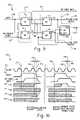
- FIGS. 1 and 2are timing diagrams illustrating a typical method for correcting duty cycle distortion in a clock and data recovery system
- FIG. 3is a block diagram of an example clock and data recovery system that automatically corrects duty cycle distortion in a data input signal
- FIG. 4is a block diagram of one alternative example clock and data recovery system that automatically corrects duty cycle distortion in a data input signal
- FIG. 5is a block diagram of another alternative example clock and data recovery system that automatically corrects duty cycle distortion in a data input signal
- FIG. 6is a block diagram of an example phase detector circuit for the clock and data recovery systems of FIGS. 3-5 ;
- FIGS. 7 and 8are timing diagrams illustrating an example operation of the phase detector circuit of FIG. 6 ;
- FIG. 9is a block diagram of an example phase detector circuit for the clock and data recovery system of FIG. 5 ;
- FIGS. 10 and 11are timing diagrams illustrating an example operation of the phase detector circuit of FIG. 9 .
- FIGS. 1 and 2are timing diagrams illustrating a method for correcting duty cycle distortion in a clock and data recovery system.
- FIGS. 1 and 2both illustrate an eye pattern for a typical data input signal 1 , 5 received by a clock and data recovery system.
- a sliced data input signal 2 , 6and a recovered clock signal 3 , 7 .
- a slicere.g., a limiting amplifier
- a recovered clock signal 3 , 7is then typically aligned in order to sample the resulting sliced data signal 2 , 6 . (See, e.g., FIG. 3-5 )
- FIG. 1illustrates a typical default setting for the slicer offset voltage 4 .
- the default slicer offset voltage 4will typically be at a zero potential.
- the default slicer offset voltage 4may not align with the crossing-point in the eye pattern of the data input signal 1 . If not corrected, the duty cycle distortion may reduce the input jitter tolerance (IJT) of the clock and data recovery circuit as a result of the sliced data signal 2 , as illustrated.
- IJTinput jitter tolerance
- FIG. 2illustrates that duty cycle distortion in the input data signal 5 may be corrected by adjusting the slicer offset voltage 8 to correspond with the crossing-point in the eye pattern of the data input signal 5 .
- Example circuits for automatically adjusting the slicer offset voltage 8 to correct duty cycle distortion in a data input signal 5are described below with reference to FIGS. 3-11 .
- FIG. 3is a block diagram of an example clock and data recovery system 10 that automatically corrects duty cycle distortion in a data input signal 26 .
- the system 10includes a slicer 12 , a phase detector circuit 14 , 16 , 18 , a first feedback circuit 20 , 22 , and a second feedback circuit 24 .
- the phase detector circuitincludes a retimer 14 , a rising edge phase detector 16 and a falling edge phase detector 18 .
- the first feedback circuitincludes a charge pump filter 20 and a phase-locking circuit 22 .
- the second feedback circuitincludes a charge pump filter 24 .
- the slicer 12is operable to receive the data input signal 26 and compare the data input signal 26 with a slicer offset voltage to generate a sliced data signal 28 .
- the slicer offset voltageis automatically adjusted by an offset control signal 38 received by the slicer 12 from the second feedback circuit 24 .
- the phase detector circuit 14 , 16 , 18is operable to receive the sliced data signal 28 from the slicer 12 and a recovered clock signal 36 from the first feedback circuit 20 , 22 to generate a rising edge output signal 32 , a falling edge output signal 34 , and a retimed data signal 30 . More specifically, the rising edge phase detector 16 generates the rising edge output signal 32 to correspond with the phase difference between the rising edge of the sliced data signal 28 and an edge of the recovered clock signal 36 . Similarly, the falling edge phase detector 18 generates the falling edge output signal 34 to correspond with the phase difference between the falling edge of the sliced data signal 28 and an edge of the recovered clock signal 36 . The retimer circuit 14 synchronizes the sliced data signal 28 with the recovered clock signal 36 to generate the retimed data signal 30 . An example phase detector circuit 14 , 16 , 18 is described below in more detail with reference to FIG. 6 .
- the first feedback circuit 20 , 22is operable to phase-lock the falling edge of the recovered clock signal 36 to the falling edges of the sliced data signal 28 .
- the first feedback circuit 20 , 22may be configured as a phase-locked loop (PLL) circuit, a delay-locked loop (DLL) circuit, or some other type of phase-locking circuit.
- PLLphase-locked loop
- DLLdelay-locked loop
- the first feedback circuitmay include a charge pump filter 20 and a voltage controlled oscillator (VCO) 22 .
- VCOvoltage controlled oscillator
- the voltage-controlled oscillator 22may receive the charge pump output signal from the charge pump filter 20 and generate the recovered clock signal 36 with a frequency that is a function of the charge pump output signal.
- the first feedback circuitis configured as a delay-locked loop (DLL)
- the circuitmay include the charge pump filter 20 , a phase interpolator 22 , and a fixed frequency signal generator such as a crystal oscillator.
- the phase interpolator 22may use the charge pump output signal from the charge pump filter 20 to control the phase of a reference clock signal from the crystal oscillator in order to generate the recovered clock signal 36 .
- a voltage or current controlled delay circuitmay be included in the delay-locked loop (DLL) in place of the phase interpolator 22 .
- the second feedback circuit 24is operable to generate the offset control signal 38 as a function of the rising edge output signal 32 .
- the second feedback circuit 24may include a charge pump filter 24 that receives the rising edge output signal 32 and generates the offset control signal 38 with a polarity corresponding to the logic level of the integrated rising edge output signal 32 . For example, if the rising edge output signal 32 is in a high logic state the majority of the time, then the charge pump filter 24 may generate a positive offset control signal 38 , causing the slicer offset level to fall. Conversely, if the rising edge output signal 32 is at a low logic state the majority of the time, then the charge pump filter 24 may generate a negative offset control signal 38 , causing the slicer offset level to rise.
- FIG. 4is a block diagram of one alternative example clock and data recovery system 50 that automatically corrects duty cycle distortion in a data input signal 26 .
- FIG. 4is similar to the clock and data recovery system 10 of FIG. 3 , except that in this system 50 the rising edge output signal 32 is configured in the first feedback circuit 20 , 22 and the falling edge output signal 34 is configured in the second feedback circuit 24 . That is, in FIG. 4 the first feedback circuit 20 , 22 is operable to phase-lock the falling edge of the recovered clock signal 36 to the rising edges of the sliced data signal 28 , and the second feedback circuit 24 is operable to generate the offset control signal 38 as a function of the falling edge output signal 34 .
- the slicer offset levelis automatically adjusted upwards when the falling edge output signal 34 is in a high logic state and is automatically adjusted downwards when the falling edge output signal 34 is in a low logic state.
- FIG. 5is a block diagram of another alternative example clock and data recovery system 60 that automatically corrects duty cycle distortion in a data input signal 26 .
- FIG. 5is similar to the clock and data recovery systems 10 , 50 shown in FIGS. 3 and 4 , except that in this system 60 both the rising edge output signal 32 and the falling edge output signal 34 are configured in each of the first feedback circuit 20 , 22 and the second feedback circuit 24 .
- the charge pump filters 20 , 24 in this embodiment 60may be two-input charge pump filters that are configured to respond to both the rising edge output signal 32 and the falling edge output signal 34 .
- the charge pump 24may be operable to adjust the slicer offset level upwards when either the rising edge output signal 32 is in a consistent low logic state, or the falling edge output signal 34 is in a consistent high logic state, and to adjust the slicer offset level downwards when either the rising edge output signal 32 is in a consistent high logic state, or the falling edge output signal 34 is in a consistent low logic state.
- the rising edge output signal 32 and the falling edge output signal 34may be combined into a single feedback signal that is input to the charge pump filters 20 , 24 in the first and/or second feedback circuit.
- the rising edge output signal 32 and the falling edge output edge output signal 34could be combined using a logic gate (e.g., an OR gate), a multiplexer (see, e.g., FIG. 9 ), by filtering and comparing the two signals 32 , 34 , or by some other suitable means.
- a logic gatee.g., an OR gate
- a multiplexersee, e.g., FIG. 9
- FIG. 6is a block diagram of an example phase detector circuit 70 , which may be used to implement the retimer 14 , rising edge phase detector 16 , and falling edge phase detector 18 in the clock and data recovery systems 10 , 50 , 60 of FIGS. 3-5 .
- the example phase detector circuit 70includes a retiming stage 71 and a synchronization stage 75 .
- the retiming stage 71includes a first retiming stage latch (D 1 ) 72 and a second retiming stage latch (D 2 ) 74
- the synchronization stage 75includes a first synchronization state latch (D 3 ) 76 and a second synchronization stage latch (D 4 ) 78 .
- the illustrated latches 72 , 74 , 76 , 78are D-type flip-flops. It should be understood, however, that other types of stage devices could also be used, such as J-type flip-flops, R-S flip-flops, shift registers, or other similar devices.
- the retiming stage 71is coupled to the sliced data signal 28 and the recovered clock signal 38 , and samples the sliced data signal 28 on the rising and falling edges of the recovered clock signal 36 to generate the retimed data signal 30 and a synchronization signal (P 1 ) 80 , respectively.
- the sliced data signal 28is coupled to the data inputs (D) of the first and second retiming stage latches 72 , 74 .
- the recovered clock signal 36is coupled to the clock input of the first retiming stage latch (D 1 ) 72
- the logical inversion of the recovered clock signal 36is coupled to the clock input of the second retiming stage latch (D 2 ) 74 .
- the first retiming stage latch (D 1 ) 72samples the sliced data signal 28 at the rising edges of the recovered clock signal 36 to generate the retimed data signal 30
- the second retiming stage latch (D 2 ) 74samples the sliced data signal 28 at the falling edges of the recovered clock signal 36 to generate the synchronization signal (P 1 ) 80 .
- the phase synchronization stage 75is coupled to the retimed data signal 30 and the synchronization signal (P 1 ) 80 , and samples the synchronization signal (P 1 ) 80 on the rising edge and falling edges of the retimed data signal 30 to generate the rising edge output signal 32 and the falling edge output signal 34 , respectively.
- the synchronization signal (P 1 ) 80is coupled to the data inputs (D) of the first and second synchronization stage latches 76 , 78 .
- the retimed data signal 30is coupled to the clock input of the first synchronization stage latch (D 3 ) 76 , and the logical inversion of the retimed data signal 30 is coupled to the clock input of the second synchronization stage latch (D 4 ) 78 .
- the first synchronization stage latch (D 3 ) 76samples the synchronization signal (P 1 ) 80 at the rising edges of the retimed data signal 30 to generate the rising edge output signal 32
- the second synchronization stage latch (D 4 ) 78samples the synchronization signal (P 1 ) 80 at the falling edges of the retimed data signal 30 to generate the falling edge output signal 34 .
- FIGS. 7 and 8are timing diagrams illustrating an example operation of the phase detector circuit 70 of FIG. 6 .
- FIG. 7illustrates an example operation of the phase detector circuit 70 in a clock and data recovery circuit 10 , as illustrated in FIG. 3 , in which a rising edge 92 , 102 of the sliced data signal 28 is out of phase with the falling clock edge 94 , 100 due to duty cycle distortion in the data signal 28 .
- FIG. 8illustrates an example operation of the phase detector circuit 70 in a clock and data recovery circuit 50 , as illustrated in FIG. 4 , in which a falling edge 126 , 132 of the sliced data signal 28 is out of phase with the falling clock edge 124 , 134 due to duty cycle distortion in the data signal 28 .
- FIGS. 7 and 8An example operation of the system 10 of FIG. 3 is further illustrated by FIGS. 7 and 8 , which are applicable to the phase detector shown in FIG. 6 .
- the falling edge of the recovered clock signal 36 generated by the clock and data recovery system 10aligns to the falling edges of the sliced input data signal 28 .
- the rising edge of the sliced input data signal 28is used to detect the duty cycle distortion through a comparison with the phase of the recovered clock signal 36 .
- FIG. 8illustrates how the first feedback circuit 20 , 22 may achieve phase lock in the system 10 .
- the falling edge output signal 34is used to determine the phase relationship between the falling data edges and the falling edge of the recovered clock signal 36 .
- the falling edge output signal 34indicated that the clock is late with respect to the falling edge of the sliced data signal 28 .
- the falling edge output signal 34indicates that the clock 36 is early with respect to the falling edge 126 of the sliced data signal 28 .
- FIG. 7demonstrates a condition in which the falling clock edges are aligned to the falling data edges 96 , 104 .
- the falling edge output signal 34has reached the equilibrium state, toggling between logic high and logic low states to keep the system 10 phase locked.
- the second feedback circuit 24uses information from the rising edge output signal 32 to cancel out the duty cycle distortion illustrated in FIG. 7 .
- the left-hand side of the illustration 90shows an example where the width of the high bit in the sliced data signal 28 is smaller than ideal, causing the rising edge 92 of the sliced data signal 28 to lag the falling edge 94 of the recovered clock signal 36 .
- the resultant phase difference 98 between the sliced data signal 28 and the recovered clock signal 36causes the phase detector circuit 70 to generate a high logic state on the rising edge output signal 32 .
- FIG. 7shows an example where the width of the high bit in the sliced data signal 28 is larger than ideal, causing the rising edge 102 of the sliced data signal 28 to lead the falling edge 100 of the recovered clock signal 36 .
- the resultant phase difference 106 between the recovered clock signal 36 and the sliced data signal 28causes the phase detector circuit 70 to generate a low logic state on the rising edge output signal 32 .
- the phase detector circuit 70used in the clock and data recovery circuit 10 , may detect if the high bit is too thin or too wide using the rising edge output signal 32 .
- the duty cycle distortion in the input data signal 26can be corrected.
- the falling edge output signal 34 illustrated in FIG. 7constantly changes between a high logic state and a low logic state because it is phase-locked with the recovered clock signal 36 , as described above with reference to FIG. 3 .
- the first feedback circuit 20 , 22forces the recovered clock signal 36 to phase-align with the falling data edges 96 , 104 .
- the left-hand side of the illustration 120shows an example wherein the width of the high bit in the sliced data signal 28 is less than ideal, causing the falling edge 126 of the sliced data signal 28 to lead the falling edge 124 of the recovered clock signal 36 .
- the resultant phase difference 128 between the recovered clock signal 36 and the sliced data signal 28causes the phase detector circuit 70 to generate a low logic state on the falling edge output signal 34 .
- the right-hand side of FIG. 8shows an example where the width of the high bit in the sliced data signal 28 is larger than ideal, causing the falling edge 132 of the sliced data signal 28 to lag the falling edge 134 of the recovered clock signal 36 .
- the resultant phase difference 136 between the sliced data signal 28 and the recovered clock signal 36causes the phase detector circuit 70 to generate a high logic state on the falling edge output signal 34 .
- the rising edge output signal 32 illustrated in FIG. 8constantly changes between a high logic state and a low logic state because it is phase-locked with the recovered clock signal 36 , as described above with reference to FIG. 4 .
- the first feedback circuit 20 , 22forces the recovered clock signal 36 to phase-align with the rising data edges 122 , 130 .
- FIG. 9is a block diagram of an example of one alternative phase detector circuit 150 for the clock and data recovery system 60 of FIG. 5 .
- This circuit 150is similar to the example phase detector circuit 70 shown in FIG. 6 , except that the phase synchronization stage 151 includes a multiplexer 152 .
- the rising edge output signal 32 and the falling edge output signal 34may be fed-back to a two-input charge pump filter 20 , 24 in the first and/or second feedback circuits, or may alternatively be combined into a single feedback signal (DN) 154 which is input to the charge pump filter(s) 20 , 24 in the first and/or second feedback circuits.
- the multiplexer 152 shown in FIG. 9provides one example circuit for combining the rising edge output signal 32 with the falling edge output signal 34 .
- the phase synchronization stage 151is coupled to the retimed data signal 30 and the synchronization signal (P 1 ) 80 , and samples the synchronization signal (P 1 ) 80 on the rising and falling edges of the retimed data signal 30 to generate the rising edge output signal (P 2 ) 32 and the falling edge output signal (P 3 ) 34 , as described above with reference to FIG. 6 .
- the rising and falling edge output signals 32 , 34are coupled as data inputs ( 1 , 0 ) of the multiplexer (M 1 ) 152 , and the retimed data signal 30 is fed forward as a select input to the multiplexer (M 1 ) 152 .
- the multiplexer (M 1 ) 152detects the rising edge of the retimed data signal 30 at its select input, the rising edge output signal (P 2 ) 32 is selected as the feedback signal (DN) 154 .
- the falling edge output signal 34is selected as the feedback signal (DN) 154 .
- FIGS. 10 and 11are timing diagrams 170 , 190 illustrating an example operation of the phase detector circuit 150 of FIG. 9 .
- FIG. 10illustrates examples in which a falling edge 174 , 182 of the sliced data signal 28 is out of phase with the falling edge 176 , 184 of the recovered clock signal 36 .
- FIG. 11illustrates examples in which a rising edge 192 , 200 of the sliced data signal 28 is out of phase with the falling edge 196 , 204 of the recovered clock signal 36 .
- the left-hand side of the illustration 170shows an example where the width of the high bits in the sliced data signal 28 are larger than ideal, causing the falling edge 174 of the sliced data signal 28 to lag the falling edge 176 of the recovered clock signal 36 .
- the resultant phase difference 178 between the recovered clock signal 36 and the sliced data signal 28causes the phase detector circuit 150 to generate a high logic level on the falling edge output signal (P 3 ) 34 and the feedback signal (DN) 154 .
- the right-hand side of FIG. 10shows an example where the width of the high bits in the sliced data signal 28 are smaller than ideal, causing a falling edge 182 of the sliced data signal 28 to lead the falling edge 184 of the recovered clock signal 36 .
- the resultant phase difference 186 between the sliced data signal 28 and the recovered clock signal 36causes the phase detector circuit 150 to generate a low logic level on the falling edge output signal (P 3 ) 34 and the feedback signal (DN) 154 .
- the left-hand side of the illustration 190shows an example where the width of the high bits in the sliced data signal 28 are larger than ideal, causing the rising edge 192 of the sliced data signal 28 to lead the falling edge 196 of the recovered clock signal 36 .
- the resultant phase difference 198 between the recovered clock signal 36 and the sliced data signal 28causes the phase detector circuit 150 to generate a low logic level on the rising edge output signal (P 2 ) 32 and the feedback signal (DN) 154 .
- the right-hand side of FIG. 11shows an example where the width of the high bits in the sliced data signal 28 are smaller than ideal, causing the rising edge 200 of the sliced data signal 28 to lag the falling edge 204 of the recovered clock signal 36 .
- the resultant phase difference 206 between the sliced data signal 28 and the recovered clock signal 36causes the phase detector circuit 150 to generate a high logic level on the rising edge output signal (P 2 ) 32 and the feedback signal (DN) 154 .
- the clock and data recovery circuits illustrated in FIGS. 3-5may include separate phase detector circuits for the first and second feedback circuits.
- the rising and falling edge output signals 32 , 34 illustrated in FIGS. 3-5may be combined by the phase detector circuit 14 , 16 , 18 to generate one or more combined feedback signal(s) input to the first and/or second feedback circuit.
Landscapes
- Engineering & Computer Science (AREA)
- Computer Networks & Wireless Communication (AREA)
- Signal Processing (AREA)
- Synchronisation In Digital Transmission Systems (AREA)
- Stabilization Of Oscillater, Synchronisation, Frequency Synthesizers (AREA)
Abstract
Description
Claims (28)
Priority Applications (1)
| Application Number | Priority Date | Filing Date | Title |
|---|---|---|---|
| US10/635,309US7292670B2 (en) | 2003-08-06 | 2003-08-06 | System and method for automatically correcting duty cycle distortion |
Applications Claiming Priority (1)
| Application Number | Priority Date | Filing Date | Title |
|---|---|---|---|
| US10/635,309US7292670B2 (en) | 2003-08-06 | 2003-08-06 | System and method for automatically correcting duty cycle distortion |
Publications (2)
| Publication Number | Publication Date |
|---|---|
| US20050031065A1 US20050031065A1 (en) | 2005-02-10 |
| US7292670B2true US7292670B2 (en) | 2007-11-06 |
Family
ID=34116216
Family Applications (1)
| Application Number | Title | Priority Date | Filing Date |
|---|---|---|---|
| US10/635,309Expired - Fee RelatedUS7292670B2 (en) | 2003-08-06 | 2003-08-06 | System and method for automatically correcting duty cycle distortion |
Country Status (1)
| Country | Link |
|---|---|
| US (1) | US7292670B2 (en) |
Cited By (8)
| Publication number | Priority date | Publication date | Assignee | Title |
|---|---|---|---|---|
| US20060140323A1 (en)* | 2004-12-28 | 2006-06-29 | Eldredge Adam B | Reducing phase offsets in a phase detector |
| US20070286321A1 (en)* | 2006-06-13 | 2007-12-13 | Gupta Atul K | Linear sample and hold phase detector for clocking circuits |
| US20100201416A1 (en)* | 2007-02-28 | 2010-08-12 | Feng Lin | Phase-generation circuitry with duty-cycle correction and method for generating a multiphase signal |
| US20110109316A1 (en)* | 2009-11-06 | 2011-05-12 | Kabushiki Kaisha Toshiba | Magnetic resonance imaging apparatus, phase comparator, control unit and coil unit |
| US8249207B1 (en)* | 2008-02-29 | 2012-08-21 | Pmc-Sierra, Inc. | Clock and data recovery sampler calibration |
| US8686764B2 (en) | 2012-02-10 | 2014-04-01 | International Business Machines Corporation | Edge selection techniques for correcting clock duty cycle |
| US9118308B1 (en) | 2014-02-07 | 2015-08-25 | Via Technologies, Inc. | Duty cycle corrector |
| US20200112465A1 (en)* | 2018-10-08 | 2020-04-09 | Nxp B.V. | Phase locked loop frequency shift keying demodulator using an auxiliary charge pump and a differential slicer |
Families Citing this family (12)
| Publication number | Priority date | Publication date | Assignee | Title |
|---|---|---|---|---|
| US7143312B1 (en)* | 2003-12-17 | 2006-11-28 | Altera Corporation | Alignment of recovered clock with data signal |
| US7486752B1 (en) | 2003-12-17 | 2009-02-03 | Altera Corporation | Alignment of clock signal with data signal |
| US7634039B2 (en)* | 2005-02-04 | 2009-12-15 | True Circuits, Inc. | Delay-locked loop with dynamically biased charge pump |
| US20060203939A1 (en)* | 2005-03-11 | 2006-09-14 | Realtek Semiconductor Corporation | Method and apparatus for correcting duty cycle distortion |
| EP1898582A1 (en)* | 2006-09-08 | 2008-03-12 | Realtek Semiconductor Corp. | Method and apparatus for correcting duty cycle distortion |
| JP4731511B2 (en)* | 2007-03-12 | 2011-07-27 | 日本電信電話株式会社 | Clock data recovery method and circuit |
| US8149978B2 (en)* | 2007-03-12 | 2012-04-03 | Nippon Telegraph And Telephone Corporation | Clock/data recovery circuit |
| US8471960B2 (en)* | 2008-11-24 | 2013-06-25 | Mediatek Inc. | Method capable of avoiding data error from incorrect sampling points |
| TWI445379B (en)* | 2010-06-02 | 2014-07-11 | Novatek Microelectronics Corp | Timing recovery controller and operation method thereof |
| US8769343B2 (en)* | 2011-06-10 | 2014-07-01 | Nxp B.V. | Compliance mode detection from limited information |
| US8934594B1 (en)* | 2013-10-14 | 2015-01-13 | Xilinx, Inc. | Sampling position tuning |
| CN105187053B (en)* | 2015-09-07 | 2017-12-22 | 电子科技大学 | A kind of metastable state and eliminate circuit for TDC |
Citations (32)
| Publication number | Priority date | Publication date | Assignee | Title |
|---|---|---|---|---|
| US4270183A (en) | 1977-02-11 | 1981-05-26 | Lockheed Aircraft Corp. | Data dejittering apparatus |
| US4805198A (en) | 1987-05-19 | 1989-02-14 | Crystal Semiconductor Corporation | Clock multiplier/jitter attenuator |
| US5077529A (en) | 1989-07-19 | 1991-12-31 | Level One Communications, Inc. | Wide bandwidth digital phase locked loop with reduced low frequency intrinsic jitter |
| US5142555A (en) | 1990-11-13 | 1992-08-25 | Dallas Semiconductor Corporation | Phase detector |
| US5150386A (en) | 1987-05-19 | 1992-09-22 | Crystal Semiconductor Corporation | Clock multiplier/jitter attenuator |
| US5329559A (en) | 1991-07-15 | 1994-07-12 | National Semiconductor | Phase detector for very high frequency clock and data recovery circuits |
| US5349612A (en) | 1992-06-19 | 1994-09-20 | Advanced Micro Devices, Inc. | Digital serializer and time delay regulator |
| US5400370A (en) | 1993-02-24 | 1995-03-21 | Advanced Micro Devices Inc. | All digital high speed algorithmic data recovery method and apparatus using locally generated compensated broad band time rulers and data edge position averaging |
| US5459753A (en) | 1992-05-06 | 1995-10-17 | 3Com Corporation | Method and apparatus for pattern independent phase detection and timing recovery |
| US5515403A (en) | 1994-06-21 | 1996-05-07 | Dsc Communications Corporation | Apparatus and method for clock alignment and switching |
| US5533072A (en) | 1993-11-12 | 1996-07-02 | International Business Machines Corporation | Digital phase alignment and integrated multichannel transceiver employing same |
| US5568526A (en) | 1994-06-17 | 1996-10-22 | International Business Machines Corporation | Self timed interface |
| US5587709A (en) | 1994-06-06 | 1996-12-24 | Deog-Kyoon Jeong | High speed serial link for fully duplexed data communication |
| US5610952A (en) | 1994-11-25 | 1997-03-11 | Hewlett-Packard Company | Synchronization signal generating device |
| US5619541A (en) | 1993-01-14 | 1997-04-08 | Apple Computer, Inc. | Delay line separator for data bus |
| US5640523A (en) | 1994-09-02 | 1997-06-17 | Cypress Semiconductor Corporation | Method and apparatus for a pulsed tri-state phase detector for reduced jitter clock recovery |
| US5644605A (en) | 1990-11-13 | 1997-07-01 | Dallas Semiconductor Corp. | Jitter attenuator |
| US5712884A (en) | 1995-03-31 | 1998-01-27 | Samsung Electronics Co., Ltd. | Data receiving method and circuit of digital communication system |
| US5712580A (en) | 1996-02-14 | 1998-01-27 | International Business Machines Corporation | Linear phase detector for half-speed quadrature clocking architecture |
| US6088415A (en) | 1998-02-23 | 2000-07-11 | National Semiconductor Corporation | Apparatus and method to adaptively equalize duty cycle distortion |
| US6101197A (en) | 1997-09-18 | 2000-08-08 | Micron Technology, Inc. | Method and apparatus for adjusting the timing of signals over fine and coarse ranges |
| US6192092B1 (en) | 1998-06-15 | 2001-02-20 | Intel Corp. | Method and apparatus for clock skew compensation |
| US6205191B1 (en) | 1997-07-21 | 2001-03-20 | Rambus Inc. | Method and apparatus for synchronizing a control signal |
| US6236696B1 (en) | 1997-05-23 | 2001-05-22 | Nec Corporation | Digital PLL circuit |
| US6285726B1 (en) | 1998-05-18 | 2001-09-04 | National Semiconductor Corporation | 10/100 mb clock recovery architecture for switches, repeaters and multi-physical layer ports |
| US6304623B1 (en) | 1998-09-03 | 2001-10-16 | Time Domain Corporation | Precision timing generator system and method |
| US6516006B1 (en) | 1999-02-16 | 2003-02-04 | Mitsubishi Electric And Electronics U.S.A., Inc. | Self-adjusting clock phase controlled architecture |
| US6526109B1 (en) | 1999-07-16 | 2003-02-25 | Conexant Systems, Inc. | Method and apparatus for hybrid smart center loop for clock data recovery |
| US20030102928A1 (en) | 2001-12-03 | 2003-06-05 | D'haene Wesley Calvin | Non-linear phase detector |
| US20030165207A1 (en)* | 2002-03-01 | 2003-09-04 | Nec Corporation | Jitter-detecting circuit, receiving circuit including the jitter-detecting circuit, and communication system |
| US20040161070A1 (en)* | 2002-08-06 | 2004-08-19 | Guangming Yin | System and method for testing the operation of a DLL-based interface |
| US7136441B2 (en)* | 2001-01-24 | 2006-11-14 | Matsushita Electric Industrial Co., Ltd. | Clock recovery circuit |
- 2003
- 2003-08-06USUS10/635,309patent/US7292670B2/ennot_activeExpired - Fee Related
Patent Citations (34)
| Publication number | Priority date | Publication date | Assignee | Title |
|---|---|---|---|---|
| US4270183A (en) | 1977-02-11 | 1981-05-26 | Lockheed Aircraft Corp. | Data dejittering apparatus |
| US4805198A (en) | 1987-05-19 | 1989-02-14 | Crystal Semiconductor Corporation | Clock multiplier/jitter attenuator |
| US5150386A (en) | 1987-05-19 | 1992-09-22 | Crystal Semiconductor Corporation | Clock multiplier/jitter attenuator |
| US5077529A (en) | 1989-07-19 | 1991-12-31 | Level One Communications, Inc. | Wide bandwidth digital phase locked loop with reduced low frequency intrinsic jitter |
| US5142555A (en) | 1990-11-13 | 1992-08-25 | Dallas Semiconductor Corporation | Phase detector |
| US5764709A (en) | 1990-11-13 | 1998-06-09 | Dallas Semiconductor Corporation | Jitter attenuator |
| US5644605A (en) | 1990-11-13 | 1997-07-01 | Dallas Semiconductor Corp. | Jitter attenuator |
| US5329559A (en) | 1991-07-15 | 1994-07-12 | National Semiconductor | Phase detector for very high frequency clock and data recovery circuits |
| US5459753A (en) | 1992-05-06 | 1995-10-17 | 3Com Corporation | Method and apparatus for pattern independent phase detection and timing recovery |
| US5349612A (en) | 1992-06-19 | 1994-09-20 | Advanced Micro Devices, Inc. | Digital serializer and time delay regulator |
| US5619541A (en) | 1993-01-14 | 1997-04-08 | Apple Computer, Inc. | Delay line separator for data bus |
| US5400370A (en) | 1993-02-24 | 1995-03-21 | Advanced Micro Devices Inc. | All digital high speed algorithmic data recovery method and apparatus using locally generated compensated broad band time rulers and data edge position averaging |
| US5533072A (en) | 1993-11-12 | 1996-07-02 | International Business Machines Corporation | Digital phase alignment and integrated multichannel transceiver employing same |
| US5587709A (en) | 1994-06-06 | 1996-12-24 | Deog-Kyoon Jeong | High speed serial link for fully duplexed data communication |
| US5568526A (en) | 1994-06-17 | 1996-10-22 | International Business Machines Corporation | Self timed interface |
| US5832047A (en) | 1994-06-17 | 1998-11-03 | International Business Machines Corporation | Self timed interface |
| US5515403A (en) | 1994-06-21 | 1996-05-07 | Dsc Communications Corporation | Apparatus and method for clock alignment and switching |
| US5640523A (en) | 1994-09-02 | 1997-06-17 | Cypress Semiconductor Corporation | Method and apparatus for a pulsed tri-state phase detector for reduced jitter clock recovery |
| US5610952A (en) | 1994-11-25 | 1997-03-11 | Hewlett-Packard Company | Synchronization signal generating device |
| US5712884A (en) | 1995-03-31 | 1998-01-27 | Samsung Electronics Co., Ltd. | Data receiving method and circuit of digital communication system |
| US5712580A (en) | 1996-02-14 | 1998-01-27 | International Business Machines Corporation | Linear phase detector for half-speed quadrature clocking architecture |
| US6236696B1 (en) | 1997-05-23 | 2001-05-22 | Nec Corporation | Digital PLL circuit |
| US6205191B1 (en) | 1997-07-21 | 2001-03-20 | Rambus Inc. | Method and apparatus for synchronizing a control signal |
| US6101197A (en) | 1997-09-18 | 2000-08-08 | Micron Technology, Inc. | Method and apparatus for adjusting the timing of signals over fine and coarse ranges |
| US6088415A (en) | 1998-02-23 | 2000-07-11 | National Semiconductor Corporation | Apparatus and method to adaptively equalize duty cycle distortion |
| US6285726B1 (en) | 1998-05-18 | 2001-09-04 | National Semiconductor Corporation | 10/100 mb clock recovery architecture for switches, repeaters and multi-physical layer ports |
| US6192092B1 (en) | 1998-06-15 | 2001-02-20 | Intel Corp. | Method and apparatus for clock skew compensation |
| US6304623B1 (en) | 1998-09-03 | 2001-10-16 | Time Domain Corporation | Precision timing generator system and method |
| US6516006B1 (en) | 1999-02-16 | 2003-02-04 | Mitsubishi Electric And Electronics U.S.A., Inc. | Self-adjusting clock phase controlled architecture |
| US6526109B1 (en) | 1999-07-16 | 2003-02-25 | Conexant Systems, Inc. | Method and apparatus for hybrid smart center loop for clock data recovery |
| US7136441B2 (en)* | 2001-01-24 | 2006-11-14 | Matsushita Electric Industrial Co., Ltd. | Clock recovery circuit |
| US20030102928A1 (en) | 2001-12-03 | 2003-06-05 | D'haene Wesley Calvin | Non-linear phase detector |
| US20030165207A1 (en)* | 2002-03-01 | 2003-09-04 | Nec Corporation | Jitter-detecting circuit, receiving circuit including the jitter-detecting circuit, and communication system |
| US20040161070A1 (en)* | 2002-08-06 | 2004-08-19 | Guangming Yin | System and method for testing the operation of a DLL-based interface |
Non-Patent Citations (3)
| Title |
|---|
| Franceschino et al., "An IF communication Circuit Tutorial", Motorola Inc. 1996, Publication # AN1539, pp. 1-8. |
| MAXIM application note 1130: Phase-lock Loop Applications Using the MAX9382, Jun. 26, 2002.* |
| Redd, Justin, "Synch and Clock Recovery-An Analog Guru Looks at Jitter", Maxim Integrated Products, Sunnyvale, California, Aug. 27, 2001, pp. 1-10. |
Cited By (16)
| Publication number | Priority date | Publication date | Assignee | Title |
|---|---|---|---|---|
| US7577224B2 (en)* | 2004-12-28 | 2009-08-18 | Silicon Laboratories Inc. | Reducing phase offsets in a phase detector |
| US20060140323A1 (en)* | 2004-12-28 | 2006-06-29 | Eldredge Adam B | Reducing phase offsets in a phase detector |
| US20070286321A1 (en)* | 2006-06-13 | 2007-12-13 | Gupta Atul K | Linear sample and hold phase detector for clocking circuits |
| US7764759B2 (en)* | 2006-06-13 | 2010-07-27 | Gennum Corporation | Linear sample and hold phase detector for clocking circuits |
| US8330508B2 (en)* | 2007-02-28 | 2012-12-11 | Micron Technology, Inc. | Phase-generation circuitry with duty-cycle correction and method for generating a multiphase signal |
| US20100201416A1 (en)* | 2007-02-28 | 2010-08-12 | Feng Lin | Phase-generation circuitry with duty-cycle correction and method for generating a multiphase signal |
| US8249207B1 (en)* | 2008-02-29 | 2012-08-21 | Pmc-Sierra, Inc. | Clock and data recovery sampler calibration |
| CN102830379A (en)* | 2009-11-06 | 2012-12-19 | 株式会社东芝 | Phase comparator |
| US20110109316A1 (en)* | 2009-11-06 | 2011-05-12 | Kabushiki Kaisha Toshiba | Magnetic resonance imaging apparatus, phase comparator, control unit and coil unit |
| CN102830379B (en)* | 2009-11-06 | 2015-01-21 | 株式会社东芝 | Phase comparator |
| US9052367B2 (en) | 2009-11-06 | 2015-06-09 | Kabushiki Kaisha Toshiba | MRI RF coil control signals modulated onto the RF coil clock signal |
| US8686764B2 (en) | 2012-02-10 | 2014-04-01 | International Business Machines Corporation | Edge selection techniques for correcting clock duty cycle |
| US8941415B2 (en) | 2012-02-10 | 2015-01-27 | International Business Machines Corporation | Edge selection techniques for correcting clock duty cycle |
| US9118308B1 (en) | 2014-02-07 | 2015-08-25 | Via Technologies, Inc. | Duty cycle corrector |
| US20200112465A1 (en)* | 2018-10-08 | 2020-04-09 | Nxp B.V. | Phase locked loop frequency shift keying demodulator using an auxiliary charge pump and a differential slicer |
| US10862720B2 (en)* | 2018-10-08 | 2020-12-08 | Nxp B.V. | Phase locked loop frequency shift keying demodulator using an auxiliary charge pump and a differential slicer |
Also Published As
| Publication number | Publication date |
|---|---|
| US20050031065A1 (en) | 2005-02-10 |
Similar Documents
| Publication | Publication Date | Title |
|---|---|---|
| US7292670B2 (en) | System and method for automatically correcting duty cycle distortion | |
| US8442178B2 (en) | Linear phase detector and clock/data recovery circuit thereof | |
| US10256967B2 (en) | Clock and data recovery circuit with jitter tolerance enhancement | |
| US8036333B2 (en) | Clock and data recovery circuit and method of recovering clocks and data | |
| US8085893B2 (en) | Low jitter clock recovery circuit | |
| US6614314B2 (en) | Non-linear phase detector | |
| US7756232B2 (en) | Clock and data recovery circuit | |
| US5406592A (en) | First order FLL/PLL system with low phase error | |
| US5579352A (en) | Simplified window de-skewing in a serial data receiver | |
| US6285219B1 (en) | Dual mode phase and frequency detector | |
| US7489171B2 (en) | Adaptive delay-locked loops and methods of generating clock signals using the same | |
| CN107078743B (en) | Circuit arrangement and method for clock and data recovery | |
| US7983370B2 (en) | Clock and data recovery circuit | |
| US11575498B2 (en) | Clock and data recovery circuits | |
| CN101247215A (en) | Technology of Extending the Dynamic Capturing and Tracking Range of Nonlinear Clock and Data Recovery Circuit | |
| EP2283575B1 (en) | Improved system and method for cycle slip prevention in a frequency synthesizer | |
| US20050046456A1 (en) | Adaptive lock position circuit | |
| US8451970B2 (en) | Variable delay circuit and delay-locked loop including the same | |
| US7283602B2 (en) | Half-rate clock and data recovery circuit | |
| KR100479309B1 (en) | Method for detecting phase difference, and apparatus for performing the same | |
| EP1544995B1 (en) | High frequency binary phase detector | |
| US7916819B2 (en) | Receiver system and method for automatic skew-tuning | |
| US7561653B2 (en) | Method and apparatus for automatic clock alignment | |
| US7359461B2 (en) | Apparatus and method for recovering clock signal from burst mode signal | |
| JP2795008B2 (en) | Input clock cutoff circuit method for phase-locked oscillation circuit |
Legal Events
| Date | Code | Title | Description |
|---|---|---|---|
| AS | Assignment | Owner name:GENNUM CORPORATION, CANADA Free format text:ASSIGNMENT OF ASSIGNORS INTEREST;ASSIGNORS:GUPTA, ATUL R.;D'HAENE, WESLEY C.;REEL/FRAME:014382/0558 Effective date:20030806 | |
| STCF | Information on status: patent grant | Free format text:PATENTED CASE | |
| FEPP | Fee payment procedure | Free format text:PAYOR NUMBER ASSIGNED (ORIGINAL EVENT CODE: ASPN); ENTITY STATUS OF PATENT OWNER: LARGE ENTITY | |
| FPAY | Fee payment | Year of fee payment:4 | |
| AS | Assignment | Owner name:SEMTECH CANADA INC., CANADA Free format text:MERGER;ASSIGNOR:GENNUM CORPORATION;REEL/FRAME:028436/0762 Effective date:20120320 | |
| AS | Assignment | Owner name:SEMTECH CANADA CORPORATION, CANADA Free format text:CHANGE OF NAME;ASSIGNOR:SEMTECH CANADA INC.;REEL/FRAME:029345/0302 Effective date:20121025 | |
| AS | Assignment | Owner name:HSBC BANK USA, NATIONAL ASSOCIATION, NEW YORK Free format text:SECURITY AGREEMENT;ASSIGNORS:SEMTECH CORPORATION;SEMTECH NEW YORK CORPORATION;SIERRA MONOLITHICS, INC.;REEL/FRAME:030341/0099 Effective date:20130502 | |
| FPAY | Fee payment | Year of fee payment:8 | |
| AS | Assignment | Owner name:HSBC BANK USA, NATIONAL ASSOCIATION, AS ADMINISTRATIVE AGENT, CALIFORNIA Free format text:SECURITY INTEREST;ASSIGNORS:SEMTECH CORPORATION;SEMTECH NEW YORK CORPORATION;SIERRA MONOLITHICS, INC.;AND OTHERS;SIGNING DATES FROM 20151115 TO 20161115;REEL/FRAME:040646/0799 Owner name:HSBC BANK USA, NATIONAL ASSOCIATION, AS ADMINISTRA Free format text:SECURITY INTEREST;ASSIGNORS:SEMTECH CORPORATION;SEMTECH NEW YORK CORPORATION;SIERRA MONOLITHICS, INC.;AND OTHERS;SIGNING DATES FROM 20151115 TO 20161115;REEL/FRAME:040646/0799 | |
| FEPP | Fee payment procedure | Free format text:MAINTENANCE FEE REMINDER MAILED (ORIGINAL EVENT CODE: REM.); ENTITY STATUS OF PATENT OWNER: LARGE ENTITY | |
| LAPS | Lapse for failure to pay maintenance fees | Free format text:PATENT EXPIRED FOR FAILURE TO PAY MAINTENANCE FEES (ORIGINAL EVENT CODE: EXP.); ENTITY STATUS OF PATENT OWNER: LARGE ENTITY | |
| STCH | Information on status: patent discontinuation | Free format text:PATENT EXPIRED DUE TO NONPAYMENT OF MAINTENANCE FEES UNDER 37 CFR 1.362 | |
| FP | Lapsed due to failure to pay maintenance fee | Effective date:20191106 | |
| AS | Assignment | Owner name:JPMORGAN CHASE BANK, N.A., AS SUCCESSOR AGENT, ILLINOIS Free format text:ASSIGNMENT OF PATENT SECURITY INTEREST PREVIOUSLY RECORDED AT REEL/FRAME (040646/0799);ASSIGNOR:HSBC BANK USA, NATIONAL ASSOCIATION, AS RESIGNING AGENT;REEL/FRAME:062781/0544 Effective date:20230210 |