US7292125B2 - MEMS based RF components and a method of construction thereof - Google Patents
MEMS based RF components and a method of construction thereofDownload PDFInfo
- Publication number
- US7292125B2 US7292125B2US11/039,860US3986005AUS7292125B2US 7292125 B2US7292125 B2US 7292125B2US 3986005 AUS3986005 AUS 3986005AUS 7292125 B2US7292125 B2US 7292125B2
- Authority
- US
- United States
- Prior art keywords
- component
- waveguide
- switch
- mems structure
- actuators
- Prior art date
- Legal status (The legal status is an assumption and is not a legal conclusion. Google has not performed a legal analysis and makes no representation as to the accuracy of the status listed.)
- Expired - Fee Related, expires
Links
- 238000000034methodMethods0.000titleclaimsabstractdescription21
- 238000010276constructionMethods0.000titleabstractdescription3
- 239000003990capacitorSubstances0.000claimsabstractdescription6
- 239000011159matrix materialSubstances0.000claimsdescription9
- PCHJSUWPFVWCPO-UHFFFAOYSA-NgoldChemical compound[Au]PCHJSUWPFVWCPO-UHFFFAOYSA-N0.000claimsdescription6
- 229910052737goldInorganic materials0.000claimsdescription6
- 239000010931goldSubstances0.000claimsdescription6
- 230000008093supporting effectEffects0.000claimsdescription5
- 230000007704transitionEffects0.000claimsdescription4
- 239000000919ceramicSubstances0.000claimsdescription2
- 238000007747platingMethods0.000claimsdescription2
- 235000012431wafersNutrition0.000description8
- 230000010354integrationEffects0.000description3
- 238000002955isolationMethods0.000description3
- 229910021420polycrystalline siliconInorganic materials0.000description3
- 229920005591polysiliconPolymers0.000description3
- 238000012546transferMethods0.000description3
- 238000013461designMethods0.000description2
- 230000000694effectsEffects0.000description2
- 230000005684electric fieldEffects0.000description2
- 230000001939inductive effectEffects0.000description2
- 210000000554irisAnatomy0.000description2
- 238000003754machiningMethods0.000description2
- 230000007246mechanismEffects0.000description2
- 238000012986modificationMethods0.000description2
- 230000004048modificationEffects0.000description2
- 238000004806packaging method and processMethods0.000description2
- 238000004088simulationMethods0.000description2
- 239000007787solidSubstances0.000description2
- 208000005647MumpsDiseases0.000description1
- XUIMIQQOPSSXEZ-UHFFFAOYSA-NSiliconChemical compound[Si]XUIMIQQOPSSXEZ-UHFFFAOYSA-N0.000description1
- YRITVODHCMDVSY-VEGPOJNRSA-N[(2r,3s,5r)-5-(6-aminopurin-9-yl)-2-(phosphonooxymethyl)oxolan-3-yl] [(2r,3s)-3-hydroxy-5-(5-methyl-2,4-dioxopyrimidin-1-yl)oxolan-2-yl]methyl hydrogen phosphateChemical compoundO=C1NC(=O)C(C)=CN1C1O[C@H](COP(O)(=O)O[C@@H]2[C@H](O[C@H](C2)N2C3=NC=NC(N)=C3N=C2)COP(O)(O)=O)[C@@H](O)C1YRITVODHCMDVSY-VEGPOJNRSA-N0.000description1
- 230000003213activating effectEffects0.000description1
- 230000005540biological transmissionEffects0.000description1
- 238000004891communicationMethods0.000description1
- 239000002184metalSubstances0.000description1
- 229910052751metalInorganic materials0.000description1
- 208000010805mumps infectious diseaseDiseases0.000description1
- 230000001902propagating effectEffects0.000description1
- 238000005096rolling processMethods0.000description1
- 229910052710siliconInorganic materials0.000description1
- 239000010703siliconSubstances0.000description1
- 239000000758substrateSubstances0.000description1
Images


Classifications
- H—ELECTRICITY
- H01—ELECTRIC ELEMENTS
- H01P—WAVEGUIDES; RESONATORS, LINES, OR OTHER DEVICES OF THE WAVEGUIDE TYPE
- H01P1/00—Auxiliary devices
- H01P1/10—Auxiliary devices for switching or interrupting
- H01P1/12—Auxiliary devices for switching or interrupting by mechanical chopper
- H01P1/122—Waveguide switches
- H—ELECTRICITY
- H01—ELECTRIC ELEMENTS
- H01P—WAVEGUIDES; RESONATORS, LINES, OR OTHER DEVICES OF THE WAVEGUIDE TYPE
- H01P1/00—Auxiliary devices
- H01P1/10—Auxiliary devices for switching or interrupting
- H01P1/12—Auxiliary devices for switching or interrupting by mechanical chopper
- H01P1/125—Coaxial switches
Definitions
- the present inventionrelates to RF MEMS microwave components and more particularly to integration of MEMS structures with signal supporting forms to develop MEMS-based RF components such as a MEMS waveguide switch.
- the present inventionrelates to a method of construction and method of operation.
- Switchesto provide signal routing and redundancy schemes to improve the reliability of both receive and transmit subsystems.
- the two types of switches that are currently being usedare mechanical switches and solid state switches.
- Mechanical (coaxial and waveguide) switchesshow good RF performance up to couple of hundred gigahertz with high power handling capability. However, they are heavy and bulky as they employ motors for the actuation mechanism.
- Solid state switcheson the other hand are relatively small in size but they show poor RF performance especially in high frequency applications (40-200 GHz) and they are limited in RF power handling.
- PIN diode waveguide switcheshave been used. They utilize incorporated PIN diodes inside the waveguide to create ON and OFF states. While these switches are small in size, they have very limited bandwidth, exhibit poor RF performance, and consume relatively high DC power.
- References to the term MEMS in this applicationrefer to a microelectromechanical system.
- RF MEMS switchesare good candidates to substitute the existing mechanical switches due to their good RF performance and miniaturized dimensions. However, their high actuating voltage and low power handling is still a major obstacle.
- the “Stand off voltage” or “self biasing” property of electrostatic MEMS switcheswhich is defined as the maximum RF voltage before pulling the beam down, is the main limiting factor in this regard.
- the high frequency rangeis considered to be from 40 to 200 GHz.
- Integrated MEMS actuatorsreplace the existing motors of mechanical waveguide and coaxial switches. It is a further object of the present invention to provide MEMS-based RF components that have a small size, light weight, high power handling and good RF performance when compared to previous devices.
- a MEMS-based RF componentcomprises a form, the form being a three dimensional waveguide.
- the formis capable of supporting a signal and has at least one of an input and output.
- the formhas a MEMS structure at least partially therein, the MEMS structure being constructed to control an RF signal within the form.
- a method of constructing a MEMS-based RF component having a three dimensional waveguide for supporting a signal and a MEMS structure at least partially thereincomprising constructing a base plate and a top cover that is sized and shaped to fit on said base plate, incorporating a MEMS structure in one of the base plate and top cover and affixing the cover to the plate to form the component.
- a method of operating a MEMS-based RF component having a three dimensional waveguide for said MEMS structure for supporting a signal and a MEMS structure at least partially therein with a controllercomprising operating said controller to move the MEMS structure to control a signal in said component.
- FIG. 1is a schematic perspective view of a MEMS-based waveguide switch
- FIG. 2is a graph of the simulation results for the switch of FIG. 1 ;
- FIG. 3 ais a schematic perspective view of a rectangular waveguide structure having transformers at an input and output;
- FIG. 3 bis a schematic side view of the switch of FIG. 3 a;
- FIG. 4 ais a top of a disassembled waveguide structure
- FIG. 4 bis a bottom view of the waveguide structure
- FIG. 4 cis a perspective view of the waveguide structure
- FIG. 5 ais a schematic perspective view of a connection of a waveguide switch into a planar circuit
- FIG. 5 bis a schematic side view of the switch of FIG. 5 a;
- FIG. 6is a schematic perspective view of a single-pole double-throw MEMS-based waveguide switch
- FIG. 7is a schematic perspective view of a MEMS-based waveguide C-switch
- FIG. 8is a graph of the measured results of the switch shown in FIG. 6 ;
- FIG. 9is a schematic perspective view of a switch matrix made up of MEMS-based on MEMS-based waveguide switches
- FIG. 10is a schematic perspective view of RF MEMS waveguide switch integrated with a planar circuit
- FIG. 11is a perspective view of an RF MEMS coaxial switch
- FIG. 12is a schematic perspective view of the switch of FIG. 10 within a bottom plate and top cover;
- FIG. 13is a schematic perspective view of a MEMS-based waveguide switch having plates that move upward or downward;
- FIG. 14is a partial schematic end view of the switch of FIG. 13 ;
- FIG. 15is a side view of the switch of FIG. 14 ;
- FIG. 16is a schematic side view of a waveguide having MEMS actuators in an OFF position
- FIG. 17is a schematic end view of the embodiment shown in FIG. 16 ;
- FIG. 18is a schematic side view of the embodiment shown in FIG. 16 with the actuators in an ON position;
- FIG. 19is a schematic end view of the embodiment shown in FIG. 18 ;
- FIG. 20is a top view of a bi-layer curled actuator
- FIG. 21is a top view of an entire actuator set of bi-layer curled actuators in an ON state
- FIG. 22is a schematic perspective view of bi-layer curled actuators in an OFF state.
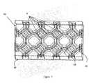
- FIG. 1shows a detailed description of the preferred embodiment of the present invention.
- a switch 2consists of a waveguide 4 and incorporated MEMS structure 6 .
- the waveguide 4could be in any type but FIG. 1 describes a single ridge waveguide configuration.
- the waveguideis constructed from two detached parts of the top cover 8 and bottom plate 10 to facilitate the MEMS structure 6 integration into the waveguide 4 .
- Top cover 8includes the ridge waveguide channel 12 and the bottom plate 10 incorporates the MEMS structure 6 .
- DC bias of the MEMS structure 6is provided through DC pins 14 that are wire-bonded 16 to actuators 18 . A DC voltage is applied to move the actuators between the OFF and ON states.
- the electric fieldis mostly concentrated in a gap 20 between a ridge 22 and the bottom plate 10 where the MEMS structure 6 is located.
- the MEMS structure 6can be based on electrostatic or thermal actuators. The requirement is to provide a good short circuit between the ridge 22 and the bottom plate 10 of the waveguide 4 for the OFF state and to remove entirely from the signal path to a position coinciding with an inner wall of the waveguide 4 for the ON state.
- FIG. 2shows the simulation results for the invention presented in FIG. 1 .
- the number of the actuatorsis based on the required isolation.
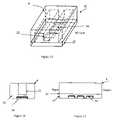
- FIGS. 3 a and 3 bTo integrate the present invention in a standard rectangular waveguide system, another embodiment is illustrated in FIGS. 3 a and 3 b .
- the same reference numeralsare used in FIGS. 3 a and 3 b as those used in FIG. 1 for those parts that are identical.
- a switch 24uses a quarter wavelength transition 26 to any standard waveguide.
- FIGS. 4 a , 4 b and 4 cshow the fabricated structure for the satellite Ku band application and using well known machining processes. For higher frequency range and millimeter wave applications, the structure is fabricated using MEMS process on wafer level. The top cover 8 of the waveguide 4 is fabricated on one wafer using deep RIE and then followed by gold plating. Another wafer is used to fabricate the MEMS unit 6 monolithically with the bottom plate of the waveguide 10 . The wafers are bonded together during the packaging stage.
- FIGS. 5 a and 5 bshow another preferred embodiment to integrate the invention into a planar circuit 28 .
- a ridge waveguide to coplanar waveguide line transition 30is used to transform the signal from waveguide switch 2 (shown in FIG. 1 ) to a planar circuit 28 .
- Line 32is a coplanar-waveguide.
- FIG. 6shows another embodiment 1 of the present invention in the form of single-pole double-throw switch 36 .
- a T junction 38is used to join the two output branches 40 .
- MEMS structures ( 42 and 44 )provides a short circuit to turn OFF one of the output ports ( 46 or 48 ) at any given time. When one output port 46 is on the other output port is off and vice-versa. This short is transferred to the T junction 38 in the form of open circuit with no effect on the transmitted signal from input 50 to the other output port ( 48 or 46 ).
- Transformers 52are located at the input 50 and output ports 46 and 48 .
- FIG. 7illustrates another configuration of the present invention in the form of a transfer switch 54 (C-type).
- This switchis designed for satellite Ku band applications. However, the switch 54 can be easily extended to higher frequency range.
- the switchis based on a multi-port waveguide 56 that incorporates four MEMS structures 58 a , 58 b , 58 c , 58 d .
- the MEMS structuresare integrated inside the waveguide 56 under the ridge (not shown in FIG. 7 ) where electric field has its maximum intensity.
- ⁇ /4 transition to ridge waveguideis utilized at the input ports 60 a , 60 b .
- Two ridge waveguide T-junctionsare used to connect the input lines (not shown) to two neighbouring ports.
- the transfer switchhas two operational states.
- ports 60 a - 60 c and 60 b - 60 dare connected and the MEMS structures of 58 c and 58 b are providing a good short circuit at the frequency range of interest. This results in high isolation between ports 60 a and 60 d and between ports 60 b and 60 c .
- An extensive effortis made to design the ridge waveguide discontinuities and the junctions in a way that the transferred impedance of the shunt irises acts as open circuit and does not interfere with the transmitted signal from port 60 a to port 60 c and from port 60 b to port 60 d .
- the other MEMS structures 58 a and 58 dare in a position to coincide with the inner wall of the waveguide 56 providing a perfect ridge waveguide transmission line.
- the operation of the switch in the state IIis very similar to that of state I except that there are through paths between ports 60 a - 60 d and between 60 b - 60 c and MEMS structures of 58 a and 58 d are shorting the waveguide.
- FIG. 8shows the measured results for the transfer switch prototype working at satellite Ku band.
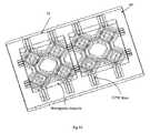
- FIG. 9shows a switch matrix 62 that is based on the present invention.
- the entire switch matrixcan be fabricated on two detached parts of a bottom plate 64 and a top cover 66 .
- the interconnect linescan be either waveguides 68 or CPW lines 32 (see to FIGS. 5 a and 5 b ).
- the bottom plate 64incorporates the MEMS structures 6 and/or the planar circuitry 28 (see FIGS. 5 a and 5 b ), and the top cover 66 includes the waveguide channels.
- Each partcan be fabricated on a separate wafer and then bonded together.
- the matrix 62is constructed from several C-switches connected together.
- FIG. 10is a schematic perspective view of a switch matrix 69 having a plurality of switches that are essentially the same as the switches in FIG. 9 .
- the MEMS waveguide switchesare integrated with a planar circuit 71 that can be coplanar waveguides, microstrip or any other type of microwave integrated circuit.
- FIG. 11shows extension of the idea to another type of switch called an RF MEMS coaxial switch 70 .
- the MEMS structure 72is incorporated in the ground shielding of the coax 74 and do not interfere with the signal for the ON state.
- a signal line 74is shorted to the ground shielding 76 - 78 and results in the OFF state of the switch.
- the switch 70can be realized by fabricating the bottom plate 80 and the MEMS structure 72 on one wafer and the top cover 82 and the central signal line 84 on another wafer.
- a low k dielectric 86can be used to separate the signal line and the ground shielding. Then, during the packaging stage, the wafers are bonded together.
- the RF MEMS coaxial switchcan be also extended to multi port MEMS coaxial switches and switch matrices (similar to the multi port MEMS waveguide switches and switch matrices).
- FIGS. 13 , 14 and 15there is shown a switch 92 having a ridge waveguide 4 with a ridge 22 and a plurality of actuators 94 on a bottom plate 10 .
- the switch 92is similar to the switch 2 shown in FIG. 1 except that the actuators of the switch 92 do not pivot but move horizontally upward and downward.
- the actuators 94are in the retracted or ON state.
- the actuatorscan be moved upward to provide a short between the top cover 4 and the bottom plate 10 , thus moving the switch to the OFF state.
- the actuators 94can be controlled to move closer to or further from the top cover 4 resulting in a controllable capacitive loading of the waveguide without shorting.
- the capacitive loading feature of the waveguidecan be used as a variable inline capacitor to design a phase shifter or other components.
- FIGS. 16 and 17there is shown a schematic side view and end view respectively of a waveguide 4 containing a post 96 with actuators 18 in the OFF state.
- FIGS. 18 and 19the same reference numerals are used and the actuators 18 are in an ON state.
- the post 96is shorted to the lower side of the waveguide and the effect of the discontinuity or post is changed. This could be from a capacitive to inductive effect depending on the size of the post.
- the embodiment shown in FIGS. 16 to 19has great potential for use as a tuning element for the filters.
- FIGS. 20 to 22there are shown bi-layer curled actuators that are designed and fabricated using the Poly MUMPs surface machining process.
- Thermally plastic deformation assembly (TPDA) methodis for the initial assembly of the beams. Afterwards, electrostatic voltage is used to roll the beams up and down.
- TPDAThermally plastic deformation assembly
- a fabricated actuator 98is composed of 1.5 ⁇ m thick poly silicon and 0.5 ⁇ m gold layer on top. The beam is about 100 ⁇ m in width and 1,500 ⁇ m in length. Initially, after the release, the bimorph of gold and poly silicon assumes a planar geometry as shown in FIG. 21 .
- the entire actuator setconsists of four rows of electrostatic actuators with each row including four bi-layer beams acting as shunt inductive irises in the OFF state.
- Application of four separate beams rather than a single platehelps to achieve better isolation in practice.
- the use of separate actuation mechanismsincreases overall contact points and hence reduces the overall contact resistance. All of the actuators and the rest of the area of the chip are covered with gold layer to reduce the loss of the silicon base substrate.
- the present inventioncan be used in high frequency devices, low frequency devices, high power devices and low power devices.
- the high frequency devicesinclude microwave, milliliter, terahertz frequencies and beyond.
- a MEMS structureis integrated with a three dimensional waveguide for RF applications. While actuators with specific types of MEMS structures are described, the invention is not limited thereto. Many types of actuators and MEMS structures will be suitable.
- the actuatorcan be a plate or a rod or strip or other convenient shape.
- the actuatorscause a short circuit between the top and bottom wall of a waveguide. However, it is not necessary in all applications of the invention for the actuators to cause a short circuit. In some applications, moving the actuators inside the waveguide will interfere sufficiently with a propagating wave in a desired manner. While the actuators have been described herein as having two positions, in some applications of the invention, more than two positions will be desirable.
- the actuatorscan be integrated in the bottom wall of a component or they can be integrated elsewhere inside the waveguide.
- the actuatorscan be located in a base plate or in a top cover and can be located on a ridge or on the side walls of a waveguide in some applications.
- a ridge waveguidecan be a single ridge waveguide or it can be a double ridge waveguide.
- the waveguidecan be coaxial, planar, low temperature cofired ceramics, coplanar, rectangular or other shape as long as it is a three dimensional waveguide that will support an RF signal.
- the actuatorscan be electrostatic, thermal, magnetic, plastic deformation type or other suitable types.
Landscapes
- Micromachines (AREA)
- Waveguide Switches, Polarizers, And Phase Shifters (AREA)
Abstract
Description
1. Field of the Invention
The present invention relates to RF MEMS microwave components and more particularly to integration of MEMS structures with signal supporting forms to develop MEMS-based RF components such as a MEMS waveguide switch. The present invention relates to a method of construction and method of operation.
2. Description of the Prior Art
Communication, wireless, and satellite payload systems employ sophisticated switch matrices to provide signal routing and redundancy schemes to improve the reliability of both receive and transmit subsystems. The two types of switches that are currently being used are mechanical switches and solid state switches. Mechanical (coaxial and waveguide) switches show good RF performance up to couple of hundred gigahertz with high power handling capability. However, they are heavy and bulky as they employ motors for the actuation mechanism. Solid state switches on the other hand are relatively small in size but they show poor RF performance especially in high frequency applications (40-200 GHz) and they are limited in RF power handling. In some applications, PIN diode waveguide switches have been used. They utilize incorporated PIN diodes inside the waveguide to create ON and OFF states. While these switches are small in size, they have very limited bandwidth, exhibit poor RF performance, and consume relatively high DC power. References to the term MEMS in this application refer to a microelectromechanical system.
RF MEMS switches are good candidates to substitute the existing mechanical switches due to their good RF performance and miniaturized dimensions. However, their high actuating voltage and low power handling is still a major obstacle. The “Stand off voltage” or “self biasing” property of electrostatic MEMS switches which is defined as the maximum RF voltage before pulling the beam down, is the main limiting factor in this regard.
It is an object of the present invention to provide a MEMS-based RF component having a form that supports a signal in combination with a MEMS structure having at least two positions that can be used to control the signal. It is a further object of the present invention to provide a MEMS-based RF component that can replace existing components in both the high frequency range, low frequency range, high power range and low power range. The high frequency range is considered to be from 40 to 200 GHz. Integrated MEMS actuators replace the existing motors of mechanical waveguide and coaxial switches. It is a further object of the present invention to provide MEMS-based RF components that have a small size, light weight, high power handling and good RF performance when compared to previous devices.
A MEMS-based RF component comprises a form, the form being a three dimensional waveguide. The form is capable of supporting a signal and has at least one of an input and output. The form has a MEMS structure at least partially therein, the MEMS structure being constructed to control an RF signal within the form.
A method of constructing a MEMS-based RF component having a three dimensional waveguide for supporting a signal and a MEMS structure at least partially therein, the method comprising constructing a base plate and a top cover that is sized and shaped to fit on said base plate, incorporating a MEMS structure in one of the base plate and top cover and affixing the cover to the plate to form the component.
A method of operating a MEMS-based RF component having a three dimensional waveguide for said MEMS structure for supporting a signal and a MEMS structure at least partially therein with a controller, the method comprising operating said controller to move the MEMS structure to control a signal in said component.
To integrate the present invention in a standard rectangular waveguide system, another embodiment is illustrated inFIGS. 3 aand3b. The same reference numerals are used inFIGS. 3 aand3bas those used inFIG. 1 for those parts that are identical. Aswitch 24 uses aquarter wavelength transition 26 to any standard waveguide.FIGS. 4 a,4band4cshow the fabricated structure for the satellite Ku band application and using well known machining processes. For higher frequency range and millimeter wave applications, the structure is fabricated using MEMS process on wafer level. Thetop cover 8 of thewaveguide 4 is fabricated on one wafer using deep RIE and then followed by gold plating. Another wafer is used to fabricate theMEMS unit 6 monolithically with the bottom plate of thewaveguide 10. The wafers are bonded together during the packaging stage.
Although this technique simplifies the integration with standard waveguide systems, it limits the bandwidth.FIGS. 5 aand5bshow another preferred embodiment to integrate the invention into aplanar circuit 28. To transform the signal from waveguide switch2 (shown inFIG. 1 ) to aplanar circuit 28, a ridge waveguide to coplanarwaveguide line transition 30 is used.Line 32 is a coplanar-waveguide.
Another preferred embodiment is shown inFIG. 9 . This shows aswitch matrix 62 that is based on the present invention. The entire switch matrix can be fabricated on two detached parts of abottom plate 64 and atop cover 66. The interconnect lines can be eitherwaveguides 68 or CPW lines32 (see toFIGS. 5 aand5b). For millimeter wave applications, thebottom plate 64 incorporates theMEMS structures 6 and/or the planar circuitry28 (seeFIGS. 5 aand5b), and thetop cover 66 includes the waveguide channels. Each part can be fabricated on a separate wafer and then bonded together. Thematrix 62 is constructed from several C-switches connected together.
Although the present invention has been fully described by way of example in connection with a preferred embodiment thereof, it should be noted that various changes and modifications will be apparent to those skilled in the art. Therefore, unless otherwise stated such changes and modifications depart from the scope of the present invention, they should be construed as being included therein. For example,FIG. 11 shows extension of the idea to another type of switch called an RF MEMScoaxial switch 70. In this embodiment, theMEMS structure 72 is incorporated in the ground shielding of the coax74 and do not interfere with the signal for the ON state. By activating theMEMS structure 72, asignal line 74 is shorted to the ground shielding76-78 and results in the OFF state of the switch. This idea can be realized by fabricating the switch in three differentdetached parts FIG. 12 can be used to realize the switch. In this configuration, theswitch 70 can be realized by fabricating thebottom plate 80 and theMEMS structure 72 on one wafer and thetop cover 82 and thecentral signal line 84 on another wafer. Alow k dielectric 86 can be used to separate the signal line and the ground shielding. Then, during the packaging stage, the wafers are bonded together. The RF MEMS coaxial switch can be also extended to multi port MEMS coaxial switches and switch matrices (similar to the multi port MEMS waveguide switches and switch matrices).
InFIGS. 13 ,14 and15, there is shown aswitch 92 having aridge waveguide 4 with aridge 22 and a plurality ofactuators 94 on abottom plate 10. Theswitch 92 is similar to theswitch 2 shown inFIG. 1 except that the actuators of theswitch 92 do not pivot but move horizontally upward and downward. As shown inFIGS. 14 and 15 , theactuators 94 are in the retracted or ON state. The actuators can be moved upward to provide a short between thetop cover 4 and thebottom plate 10, thus moving the switch to the OFF state. As an alternative, theactuators 94 can be controlled to move closer to or further from thetop cover 4 resulting in a controllable capacitive loading of the waveguide without shorting. The capacitive loading feature of the waveguide can be used as a variable inline capacitor to design a phase shifter or other components.
InFIGS. 16 and 17 , there is shown a schematic side view and end view respectively of awaveguide 4 containing apost 96 withactuators 18 in the OFF state. InFIGS. 18 and 19 , the same reference numerals are used and theactuators 18 are in an ON state. By moving the actuators to the position shown inFIGS. 16 and 17 , thepost 96 is shorted to the lower side of the waveguide and the effect of the discontinuity or post is changed. This could be from a capacitive to inductive effect depending on the size of the post. The embodiment shown inFIGS. 16 to 19 has great potential for use as a tuning element for the filters.
InFIGS. 20 to 22 there are shown bi-layer curled actuators that are designed and fabricated using the Poly MUMPs surface machining process. Thermally plastic deformation assembly (TPDA) method is for the initial assembly of the beams. Afterwards, electrostatic voltage is used to roll the beams up and down. InFIG. 20 , a fabricatedactuator 98 is composed of 1.5 μm thick poly silicon and 0.5 μm gold layer on top. The beam is about 100 μm in width and 1,500 μm in length. Initially, after the release, the bimorph of gold and poly silicon assumes a planar geometry as shown inFIG. 21 . When exposed to higher temperature (approximately 200° for ten minutes), the metal yields and upon the relaxation, a new stress mismatch results in a deformed beam toward the gold layer (top layer). This results in a curled beam or actuator as shown inFIG. 22 . Another poly silicon layer (poly 0) under the beam is used as the electrode layer. To prevent the beam from collapsing to the bottom electrode, two stopper steps at both side edges of the beams are utilized. At the down position, these two steps contact the lower surface of the chip and stop the beam from unwanted collapse to the electrodes underneath. A voltage of approximately 20 volts seems to be required to roll the beam down. Upon the application of DC voltage, the beam starts rolling down until the entire beam coincides with the bottom surface of the chip. The entire actuator set consists of four rows of electrostatic actuators with each row including four bi-layer beams acting as shunt inductive irises in the OFF state. Application of four separate beams rather than a single plate helps to achieve better isolation in practice. The use of separate actuation mechanisms increases overall contact points and hence reduces the overall contact resistance. All of the actuators and the rest of the area of the chip are covered with gold layer to reduce the loss of the silicon base substrate.
The present invention can be used in high frequency devices, low frequency devices, high power devices and low power devices. The high frequency devices include microwave, milliliter, terahertz frequencies and beyond.
With the present invention, a MEMS structure is integrated with a three dimensional waveguide for RF applications. While actuators with specific types of MEMS structures are described, the invention is not limited thereto. Many types of actuators and MEMS structures will be suitable. The actuator can be a plate or a rod or strip or other convenient shape. In some embodiments, the actuators cause a short circuit between the top and bottom wall of a waveguide. However, it is not necessary in all applications of the invention for the actuators to cause a short circuit. In some applications, moving the actuators inside the waveguide will interfere sufficiently with a propagating wave in a desired manner. While the actuators have been described herein as having two positions, in some applications of the invention, more than two positions will be desirable. The actuators can be integrated in the bottom wall of a component or they can be integrated elsewhere inside the waveguide. The actuators can be located in a base plate or in a top cover and can be located on a ridge or on the side walls of a waveguide in some applications.
A ridge waveguide can be a single ridge waveguide or it can be a double ridge waveguide. The waveguide can be coaxial, planar, low temperature cofired ceramics, coplanar, rectangular or other shape as long as it is a three dimensional waveguide that will support an RF signal. The actuators can be electrostatic, thermal, magnetic, plastic deformation type or other suitable types.
Claims (41)
1. A MEMS-based RF component comprising a form, said form being a three dimensional waveguide having at least one inner wall surrounding said waveguide, said at least one inner wall being conductive, said form being capable of supporting a signal and having at least one of an input and output, said form having a MEMS structure at least partially therein, said MEMS structure being constructed to control an RF signal within said form while all inner walls of said at least one inner wall remain conductive.
2. A component as claimed inclaim 1 wherein said MEMS structure has a first position and a second position.
3. A component as claimed inclaim 2 wherein there is a controller to control movement of said MEMS structure.
4. A component as claimed inclaim 3 wherein said MEMS structure has a plurality of actuators, said actuators being movable between said first position and said second position.
5. A component as claimed inclaim 3 wherein said MEMS structure is located in said waveguide.
6. A component as claimed inclaim 3 wherein said MEMS structure is integrated with said waveguide.
7. A component as claimed inclaim 3 wherein said waveguide is at least one of a rectangular waveguide, a coaxial waveguide, a ridge waveguide, a single ridge waveguide and a double ridge waveguide.
8. A component as claimed inclaim 7 wherein the component is one selected from the group of a switch, capacitor, variable capacitor, phase shifter and filter.
9. A component as claimed inclaim 3 wherein said component is a switch, said form has a signal pat and said MEMS structure is located out of said pat in said first position and at least partially within said path in said second position.
10. A component as claimed inclaim 9 wherein said switch is on in said first position and off in said second position.
11. A component as claimed inclaim 8 wherein said component is a switch selected from the group of an R-switch, C-switch, a T-switch, single pole single throw switch, single pole double throw switch, switch matrix and coaxial switch, planar switch and waveguide switch integrated with a planar circuit.
12. A component as claimed inclaim 4 wherein said actuators are at least one selected from the group of thermal, magnetic, electrostatic, curling actuators and plastic deformation type of actuators.
13. A component as claimed inclaim 6 wherein said component is a C-switch with two input ports and two output ports of said at least one of an input and an output.
14. A component as claimed inclaim 6 wherein said switch is a T-switch with two input ports and two output ports of said at least one of an input and output.
15. A component as claimed inclaim 6 wherein said component is an R-switch with a maximum of two input ports and two output ports of said at least one of an input and output in any single position of said switch.
16. A component as claimed inclaim 6 wherein said component is a coaxial switch with at least one input and at least one output of said at least one input and output.
17. A component as claimed inclaim 6 wherein said component is a single pole double throw switch having one input and two outputs of said at least one input and output.
18. A component as claimed inclaim 3 wherein said component has a ridge waveguide channel therein with a gap located above a bottom plate, said MEMS structure being located beneath said gap.
19. A component as claimed inclaim 18 wherein said component has a top that is sized and shaped to fit onto said bottom plate, said ridge waveguide being located in said top.
20. A component as claimed inclaim 3 wherein said component has at least one input port and at least one output port of said at least one input and output, said ports having transformers located therein.
21. A component as claimed inclaim 4 wherein said actuators are constructed to short circuit said signal path to turn said switch off.
22. A component as claimed inclaim 10 wherein said component has more than one signal path with a MEMS structure located at each signal path, said MEMS structure having actuators that are constructed to short circuit a signal path in which the actuators are located when said signal path is off.
23. A component as claimed inclaim 22 wherein said actuators are constructed to be located outside of a signal path when said signal path is on.
24. A component as claimed inclaim 19 wherein said top has gold plating thereon.
25. A component as claimed inclaim 4 wherein said actuators are movable up and down in a switch to provide a short between a top and bottom plate when said switch is off and to be removed entirely to a position coinciding with said inner wall of a said waveguide when said switch is on, said actuators having a capacitive loading.
26. A component as claimed inclaim 4 wherein said actuators are controlled to adjust an elevation of said actuators resulting an a controllable capacitative loading of said waveguide.
27. A component as claimed inclaim 4 wherein said actuators are located and constructed to provide a variable inline capacitor.
28. A component as claimed inclaim 27 wherein the variable inline capacitor is located in one of a phase shifter, tunable filter, matching network and any reconfigurable system.
29. A component as claimed inclaim 1 wherein said component is constructed for use in a waveband selected from the group of microwave, millimeter, terahertz and beyond.
30. A component as claimed inclaim 4 wherein the component is a switch matrix comprised of a plurality of switches that are interconnected to one another, said switch matrix having a plurality of inputs and a plurality of outputs of said at least one input and output, the plurality of switches in said switch matrix having a MEMS structure with a plurality of actuators that are movable between a first position and a second position.
31. A component as claimed inclaim 3 wherein said component has a configuration that is selected from the group of a planar configuration, a coplanar-waveguide configuration and low temperature cofired ceramic configuration.
32. A component as claimed inclaim 1 wherein the MTEMS structure is integrated on a planar circuit.
33. A component as claimed inclaim 1 wherein the component is a wide-band ridge waveguide connected into a coplanar waveguide line transition.
34. A component as claimed inclaim 33 wherein said MEMS structure is integrated onto a bottom plate and a waveguide channel and ridge are fabricated on a top cover.
35. A component as claimed inclaim 34 wherein a microstrip line is used as an interface to transform a ridge waveguide mode to a coplanar waveguide mode.
36. A method of constructing a MEMS-based RF component having a three dimensional waveguide with a MEMS structure at least partially therein, said waveguide having at least one wall surrounding said waveguide, said at least one wall being conductive, said method comprising constructing a base plate and a top cover that is sized and shaped to fit on said base plate, one of said base plate and said top cover having a MEMS structure incorporated therein, and affixing said cover to said plate to form said component, constructing said MEMS structure so that said at least one wall remains conducting as said MEMS structure generates.
37. A method as claimed inclaim 36 including the step of incorporating the MEMS structure in said base plate and incorporating a waveguide in said cover.
38. A method as claim inclaim 37 including the step of incorporating a ridge waveguide in said cover.
39. A method as claimed inclaim 37 including the step of fabricating the MEMS structure, the cover and the base plate by the same process monolithically.
40. A method as claimed inclaim 36 including the steps of constructing the MEMS structure separately from said cover.
41. A method of operating an RF component having a form that is a three dimensional waveguide, said waveguide having at least one inner wall surrounding said waveguide, said at least one wall being conductive, said form having a MEMS structure at least partially therein with a controller for said MEMS structure, said method comprising operating said controller to move said MEMS structure to control an RF signal within said form while all inner walls of said at least one inner wall remain conductive.
Priority Applications (1)
| Application Number | Priority Date | Filing Date | Title |
|---|---|---|---|
| US11/039,860US7292125B2 (en) | 2004-01-22 | 2005-01-24 | MEMS based RF components and a method of construction thereof |
Applications Claiming Priority (2)
| Application Number | Priority Date | Filing Date | Title |
|---|---|---|---|
| US53790404P | 2004-01-22 | 2004-01-22 | |
| US11/039,860US7292125B2 (en) | 2004-01-22 | 2005-01-24 | MEMS based RF components and a method of construction thereof |
Publications (2)
| Publication Number | Publication Date |
|---|---|
| US20050201672A1 US20050201672A1 (en) | 2005-09-15 |
| US7292125B2true US7292125B2 (en) | 2007-11-06 |
Family
ID=34633023
Family Applications (1)
| Application Number | Title | Priority Date | Filing Date |
|---|---|---|---|
| US11/039,860Expired - Fee RelatedUS7292125B2 (en) | 2004-01-22 | 2005-01-24 | MEMS based RF components and a method of construction thereof |
Country Status (2)
| Country | Link |
|---|---|
| US (1) | US7292125B2 (en) |
| EP (1) | EP1557900A1 (en) |
Cited By (138)
| Publication number | Priority date | Publication date | Assignee | Title |
|---|---|---|---|---|
| US7733265B2 (en) | 2008-04-04 | 2010-06-08 | Toyota Motor Engineering & Manufacturing North America, Inc. | Three dimensional integrated automotive radars and methods of manufacturing the same |
| US20100156577A1 (en)* | 2008-12-22 | 2010-06-24 | General Electric Company | Micro-electromechanical system switch |
| US7830301B2 (en) | 2008-04-04 | 2010-11-09 | Toyota Motor Engineering & Manufacturing North America, Inc. | Dual-band antenna array and RF front-end for automotive radars |
| US20110050371A1 (en)* | 2009-08-29 | 2011-03-03 | William Roland Deal | Monolithically integrated active electronic circuit and waveguide structure for terahertz frequencies |
| US7990237B2 (en) | 2009-01-16 | 2011-08-02 | Toyota Motor Engineering & Manufacturing North America, Inc. | System and method for improving performance of coplanar waveguide bends at mm-wave frequencies |
| US8022861B2 (en) | 2008-04-04 | 2011-09-20 | Toyota Motor Engineering & Manufacturing North America, Inc. | Dual-band antenna array and RF front-end for mm-wave imager and radar |
| US20130321096A1 (en)* | 2012-06-05 | 2013-12-05 | Mohamed M. Fahmi | Compact Multiport Waveguide Switches |
| US8786496B2 (en) | 2010-07-28 | 2014-07-22 | Toyota Motor Engineering & Manufacturing North America, Inc. | Three-dimensional array antenna on a substrate with enhanced backlobe suppression for mm-wave automotive applications |
| US9667317B2 (en) | 2015-06-15 | 2017-05-30 | At&T Intellectual Property I, L.P. | Method and apparatus for providing security using network traffic adjustments |
| US9674711B2 (en) | 2013-11-06 | 2017-06-06 | At&T Intellectual Property I, L.P. | Surface-wave communications and methods thereof |
| US9685992B2 (en) | 2014-10-03 | 2017-06-20 | At&T Intellectual Property I, L.P. | Circuit panel network and methods thereof |
| US9705561B2 (en) | 2015-04-24 | 2017-07-11 | At&T Intellectual Property I, L.P. | Directional coupling device and methods for use therewith |
| US9705610B2 (en) | 2014-10-21 | 2017-07-11 | At&T Intellectual Property I, L.P. | Transmission device with impairment compensation and methods for use therewith |
| US9722318B2 (en) | 2015-07-14 | 2017-08-01 | At&T Intellectual Property I, L.P. | Method and apparatus for coupling an antenna to a device |
| US9729197B2 (en) | 2015-10-01 | 2017-08-08 | At&T Intellectual Property I, L.P. | Method and apparatus for communicating network management traffic over a network |
| US9735833B2 (en) | 2015-07-31 | 2017-08-15 | At&T Intellectual Property I, L.P. | Method and apparatus for communications management in a neighborhood network |
| US9742521B2 (en) | 2014-11-20 | 2017-08-22 | At&T Intellectual Property I, L.P. | Transmission device with mode division multiplexing and methods for use therewith |
| US9742462B2 (en) | 2014-12-04 | 2017-08-22 | At&T Intellectual Property I, L.P. | Transmission medium and communication interfaces and methods for use therewith |
| US9749013B2 (en) | 2015-03-17 | 2017-08-29 | At&T Intellectual Property I, L.P. | Method and apparatus for reducing attenuation of electromagnetic waves guided by a transmission medium |
| US9748626B2 (en) | 2015-05-14 | 2017-08-29 | At&T Intellectual Property I, L.P. | Plurality of cables having different cross-sectional shapes which are bundled together to form a transmission medium |
| US9749053B2 (en) | 2015-07-23 | 2017-08-29 | At&T Intellectual Property I, L.P. | Node device, repeater and methods for use therewith |
| US9769128B2 (en) | 2015-09-28 | 2017-09-19 | At&T Intellectual Property I, L.P. | Method and apparatus for encryption of communications over a network |
| US9768833B2 (en) | 2014-09-15 | 2017-09-19 | At&T Intellectual Property I, L.P. | Method and apparatus for sensing a condition in a transmission medium of electromagnetic waves |
| US9769020B2 (en) | 2014-10-21 | 2017-09-19 | At&T Intellectual Property I, L.P. | Method and apparatus for responding to events affecting communications in a communication network |
| US9780834B2 (en) | 2014-10-21 | 2017-10-03 | At&T Intellectual Property I, L.P. | Method and apparatus for transmitting electromagnetic waves |
| US9787412B2 (en) | 2015-06-25 | 2017-10-10 | At&T Intellectual Property I, L.P. | Methods and apparatus for inducing a fundamental wave mode on a transmission medium |
| US9793954B2 (en) | 2015-04-28 | 2017-10-17 | At&T Intellectual Property I, L.P. | Magnetic coupling device and methods for use therewith |
| US9793951B2 (en) | 2015-07-15 | 2017-10-17 | At&T Intellectual Property I, L.P. | Method and apparatus for launching a wave mode that mitigates interference |
| US9793955B2 (en) | 2015-04-24 | 2017-10-17 | At&T Intellectual Property I, Lp | Passive electrical coupling device and methods for use therewith |
| US9800327B2 (en) | 2014-11-20 | 2017-10-24 | At&T Intellectual Property I, L.P. | Apparatus for controlling operations of a communication device and methods thereof |
| US9820146B2 (en) | 2015-06-12 | 2017-11-14 | At&T Intellectual Property I, L.P. | Method and apparatus for authentication and identity management of communicating devices |
| US9838896B1 (en) | 2016-12-09 | 2017-12-05 | At&T Intellectual Property I, L.P. | Method and apparatus for assessing network coverage |
| US9838078B2 (en) | 2015-07-31 | 2017-12-05 | At&T Intellectual Property I, L.P. | Method and apparatus for exchanging communication signals |
| US9847566B2 (en) | 2015-07-14 | 2017-12-19 | At&T Intellectual Property I, L.P. | Method and apparatus for adjusting a field of a signal to mitigate interference |
| US9847850B2 (en) | 2014-10-14 | 2017-12-19 | At&T Intellectual Property I, L.P. | Method and apparatus for adjusting a mode of communication in a communication network |
| US9853342B2 (en) | 2015-07-14 | 2017-12-26 | At&T Intellectual Property I, L.P. | Dielectric transmission medium connector and methods for use therewith |
| US9860075B1 (en) | 2016-08-26 | 2018-01-02 | At&T Intellectual Property I, L.P. | Method and communication node for broadband distribution |
| US9865911B2 (en) | 2015-06-25 | 2018-01-09 | At&T Intellectual Property I, L.P. | Waveguide system for slot radiating first electromagnetic waves that are combined into a non-fundamental wave mode second electromagnetic wave on a transmission medium |
| US9866276B2 (en) | 2014-10-10 | 2018-01-09 | At&T Intellectual Property I, L.P. | Method and apparatus for arranging communication sessions in a communication system |
| US9866309B2 (en) | 2015-06-03 | 2018-01-09 | At&T Intellectual Property I, Lp | Host node device and methods for use therewith |
| US9871282B2 (en) | 2015-05-14 | 2018-01-16 | At&T Intellectual Property I, L.P. | At least one transmission medium having a dielectric surface that is covered at least in part by a second dielectric |
| US9871283B2 (en) | 2015-07-23 | 2018-01-16 | At&T Intellectual Property I, Lp | Transmission medium having a dielectric core comprised of plural members connected by a ball and socket configuration |
| US9871558B2 (en) | 2014-10-21 | 2018-01-16 | At&T Intellectual Property I, L.P. | Guided-wave transmission device and methods for use therewith |
| US9876264B2 (en) | 2015-10-02 | 2018-01-23 | At&T Intellectual Property I, Lp | Communication system, guided wave switch and methods for use therewith |
| US9876570B2 (en) | 2015-02-20 | 2018-01-23 | At&T Intellectual Property I, Lp | Guided-wave transmission device with non-fundamental mode propagation and methods for use therewith |
| US9876605B1 (en) | 2016-10-21 | 2018-01-23 | At&T Intellectual Property I, L.P. | Launcher and coupling system to support desired guided wave mode |
| US9882257B2 (en) | 2015-07-14 | 2018-01-30 | At&T Intellectual Property I, L.P. | Method and apparatus for launching a wave mode that mitigates interference |
| US9887447B2 (en) | 2015-05-14 | 2018-02-06 | At&T Intellectual Property I, L.P. | Transmission medium having multiple cores and methods for use therewith |
| US9893795B1 (en) | 2016-12-07 | 2018-02-13 | At&T Intellectual Property I, Lp | Method and repeater for broadband distribution |
| US9906269B2 (en) | 2014-09-17 | 2018-02-27 | At&T Intellectual Property I, L.P. | Monitoring and mitigating conditions in a communication network |
| US9904535B2 (en) | 2015-09-14 | 2018-02-27 | At&T Intellectual Property I, L.P. | Method and apparatus for distributing software |
| US9911020B1 (en) | 2016-12-08 | 2018-03-06 | At&T Intellectual Property I, L.P. | Method and apparatus for tracking via a radio frequency identification device |
| US9913139B2 (en) | 2015-06-09 | 2018-03-06 | At&T Intellectual Property I, L.P. | Signal fingerprinting for authentication of communicating devices |
| US9912381B2 (en) | 2015-06-03 | 2018-03-06 | At&T Intellectual Property I, Lp | Network termination and methods for use therewith |
| US9912033B2 (en) | 2014-10-21 | 2018-03-06 | At&T Intellectual Property I, Lp | Guided wave coupler, coupling module and methods for use therewith |
| US9912027B2 (en) | 2015-07-23 | 2018-03-06 | At&T Intellectual Property I, L.P. | Method and apparatus for exchanging communication signals |
| US9917341B2 (en) | 2015-05-27 | 2018-03-13 | At&T Intellectual Property I, L.P. | Apparatus and method for launching electromagnetic waves and for modifying radial dimensions of the propagating electromagnetic waves |
| US9927517B1 (en) | 2016-12-06 | 2018-03-27 | At&T Intellectual Property I, L.P. | Apparatus and methods for sensing rainfall |
| US9929755B2 (en) | 2015-07-14 | 2018-03-27 | At&T Intellectual Property I, L.P. | Method and apparatus for coupling an antenna to a device |
| US9948333B2 (en) | 2015-07-23 | 2018-04-17 | At&T Intellectual Property I, L.P. | Method and apparatus for wireless communications to mitigate interference |
| US9954287B2 (en) | 2014-11-20 | 2018-04-24 | At&T Intellectual Property I, L.P. | Apparatus for converting wireless signals and electromagnetic waves and methods thereof |
| US9954286B2 (en) | 2014-10-21 | 2018-04-24 | At&T Intellectual Property I, L.P. | Guided-wave transmission device with non-fundamental mode propagation and methods for use therewith |
| US9967173B2 (en) | 2015-07-31 | 2018-05-08 | At&T Intellectual Property I, L.P. | Method and apparatus for authentication and identity management of communicating devices |
| US9973416B2 (en) | 2014-10-02 | 2018-05-15 | At&T Intellectual Property I, L.P. | Method and apparatus that provides fault tolerance in a communication network |
| US9973940B1 (en) | 2017-02-27 | 2018-05-15 | At&T Intellectual Property I, L.P. | Apparatus and methods for dynamic impedance matching of a guided wave launcher |
| US9985331B2 (en)* | 2015-07-07 | 2018-05-29 | Huawei Technologies Co., Ltd. | Substrate integrated waveguide switch |
| US9991580B2 (en) | 2016-10-21 | 2018-06-05 | At&T Intellectual Property I, L.P. | Launcher and coupling system for guided wave mode cancellation |
| US9997819B2 (en) | 2015-06-09 | 2018-06-12 | At&T Intellectual Property I, L.P. | Transmission medium and method for facilitating propagation of electromagnetic waves via a core |
| US9999038B2 (en) | 2013-05-31 | 2018-06-12 | At&T Intellectual Property I, L.P. | Remote distributed antenna system |
| US9998870B1 (en) | 2016-12-08 | 2018-06-12 | At&T Intellectual Property I, L.P. | Method and apparatus for proximity sensing |
| US10009067B2 (en) | 2014-12-04 | 2018-06-26 | At&T Intellectual Property I, L.P. | Method and apparatus for configuring a communication interface |
| US10020844B2 (en) | 2016-12-06 | 2018-07-10 | T&T Intellectual Property I, L.P. | Method and apparatus for broadcast communication via guided waves |
| US10027397B2 (en) | 2016-12-07 | 2018-07-17 | At&T Intellectual Property I, L.P. | Distributed antenna system and methods for use therewith |
| US10044409B2 (en) | 2015-07-14 | 2018-08-07 | At&T Intellectual Property I, L.P. | Transmission medium and methods for use therewith |
| US10051630B2 (en) | 2013-05-31 | 2018-08-14 | At&T Intellectual Property I, L.P. | Remote distributed antenna system |
| US10069185B2 (en) | 2015-06-25 | 2018-09-04 | At&T Intellectual Property I, L.P. | Methods and apparatus for inducing a non-fundamental wave mode on a transmission medium |
| US10069535B2 (en) | 2016-12-08 | 2018-09-04 | At&T Intellectual Property I, L.P. | Apparatus and methods for launching electromagnetic waves having a certain electric field structure |
| US10090594B2 (en) | 2016-11-23 | 2018-10-02 | At&T Intellectual Property I, L.P. | Antenna system having structural configurations for assembly |
| US10090606B2 (en) | 2015-07-15 | 2018-10-02 | At&T Intellectual Property I, L.P. | Antenna system with dielectric array and methods for use therewith |
| US10096883B2 (en) | 2016-12-06 | 2018-10-09 | At&T Intellectual Property I, L.P. | Methods and apparatus for adjusting a wavelength electromagnetic waves |
| US10103422B2 (en) | 2016-12-08 | 2018-10-16 | At&T Intellectual Property I, L.P. | Method and apparatus for mounting network devices |
| US10135145B2 (en) | 2016-12-06 | 2018-11-20 | At&T Intellectual Property I, L.P. | Apparatus and methods for generating an electromagnetic wave along a transmission medium |
| US10135147B2 (en) | 2016-10-18 | 2018-11-20 | At&T Intellectual Property I, L.P. | Apparatus and methods for launching guided waves via an antenna |
| US10135146B2 (en) | 2016-10-18 | 2018-11-20 | At&T Intellectual Property I, L.P. | Apparatus and methods for launching guided waves via circuits |
| US10139820B2 (en) | 2016-12-07 | 2018-11-27 | At&T Intellectual Property I, L.P. | Method and apparatus for deploying equipment of a communication system |
| US10148016B2 (en) | 2015-07-14 | 2018-12-04 | At&T Intellectual Property I, L.P. | Apparatus and methods for communicating utilizing an antenna array |
| US10168695B2 (en) | 2016-12-07 | 2019-01-01 | At&T Intellectual Property I, L.P. | Method and apparatus for controlling an unmanned aircraft |
| US10178445B2 (en) | 2016-11-23 | 2019-01-08 | At&T Intellectual Property I, L.P. | Methods, devices, and systems for load balancing between a plurality of waveguides |
| US10205655B2 (en) | 2015-07-14 | 2019-02-12 | At&T Intellectual Property I, L.P. | Apparatus and methods for communicating utilizing an antenna array and multiple communication paths |
| US10205212B2 (en) | 2016-12-06 | 2019-02-12 | At&T Intellectual Property I, L.P. | Methods and apparatus for adjusting a phase of electromagnetic waves |
| US10225025B2 (en) | 2016-11-03 | 2019-03-05 | At&T Intellectual Property I, L.P. | Method and apparatus for detecting a fault in a communication system |
| US10224634B2 (en) | 2016-11-03 | 2019-03-05 | At&T Intellectual Property I, L.P. | Methods and apparatus for adjusting an operational characteristic of an antenna |
| US10243270B2 (en) | 2016-12-07 | 2019-03-26 | At&T Intellectual Property I, L.P. | Beam adaptive multi-feed dielectric antenna system and methods for use therewith |
| US10243784B2 (en) | 2014-11-20 | 2019-03-26 | At&T Intellectual Property I, L.P. | System for generating topology information and methods thereof |
| US10264586B2 (en) | 2016-12-09 | 2019-04-16 | At&T Mobility Ii Llc | Cloud-based packet controller and methods for use therewith |
| US10291334B2 (en) | 2016-11-03 | 2019-05-14 | At&T Intellectual Property I, L.P. | System for detecting a fault in a communication system |
| US10298293B2 (en) | 2017-03-13 | 2019-05-21 | At&T Intellectual Property I, L.P. | Apparatus of communication utilizing wireless network devices |
| US10305190B2 (en) | 2016-12-01 | 2019-05-28 | At&T Intellectual Property I, L.P. | Reflecting dielectric antenna system and methods for use therewith |
| US10312567B2 (en) | 2016-10-26 | 2019-06-04 | At&T Intellectual Property I, L.P. | Launcher with planar strip antenna and methods for use therewith |
| US10326689B2 (en) | 2016-12-08 | 2019-06-18 | At&T Intellectual Property I, L.P. | Method and system for providing alternative communication paths |
| US10326494B2 (en) | 2016-12-06 | 2019-06-18 | At&T Intellectual Property I, L.P. | Apparatus for measurement de-embedding and methods for use therewith |
| US10340601B2 (en) | 2016-11-23 | 2019-07-02 | At&T Intellectual Property I, L.P. | Multi-antenna system and methods for use therewith |
| US10340983B2 (en) | 2016-12-09 | 2019-07-02 | At&T Intellectual Property I, L.P. | Method and apparatus for surveying remote sites via guided wave communications |
| US10340573B2 (en) | 2016-10-26 | 2019-07-02 | At&T Intellectual Property I, L.P. | Launcher with cylindrical coupling device and methods for use therewith |
| US10340603B2 (en) | 2016-11-23 | 2019-07-02 | At&T Intellectual Property I, L.P. | Antenna system having shielded structural configurations for assembly |
| US10355367B2 (en) | 2015-10-16 | 2019-07-16 | At&T Intellectual Property I, L.P. | Antenna structure for exchanging wireless signals |
| US10361489B2 (en) | 2016-12-01 | 2019-07-23 | At&T Intellectual Property I, L.P. | Dielectric dish antenna system and methods for use therewith |
| US10359749B2 (en) | 2016-12-07 | 2019-07-23 | At&T Intellectual Property I, L.P. | Method and apparatus for utilities management via guided wave communication |
| US10374316B2 (en) | 2016-10-21 | 2019-08-06 | At&T Intellectual Property I, L.P. | System and dielectric antenna with non-uniform dielectric |
| US10382976B2 (en) | 2016-12-06 | 2019-08-13 | At&T Intellectual Property I, L.P. | Method and apparatus for managing wireless communications based on communication paths and network device positions |
| US10389029B2 (en) | 2016-12-07 | 2019-08-20 | At&T Intellectual Property I, L.P. | Multi-feed dielectric antenna system with core selection and methods for use therewith |
| US10389037B2 (en) | 2016-12-08 | 2019-08-20 | At&T Intellectual Property I, L.P. | Apparatus and methods for selecting sections of an antenna array and use therewith |
| US10411356B2 (en) | 2016-12-08 | 2019-09-10 | At&T Intellectual Property I, L.P. | Apparatus and methods for selectively targeting communication devices with an antenna array |
| US10439675B2 (en) | 2016-12-06 | 2019-10-08 | At&T Intellectual Property I, L.P. | Method and apparatus for repeating guided wave communication signals |
| US10446936B2 (en) | 2016-12-07 | 2019-10-15 | At&T Intellectual Property I, L.P. | Multi-feed dielectric antenna system and methods for use therewith |
| US10498044B2 (en) | 2016-11-03 | 2019-12-03 | At&T Intellectual Property I, L.P. | Apparatus for configuring a surface of an antenna |
| US10531357B2 (en) | 2018-03-26 | 2020-01-07 | At&T Intellectual Property I, L.P. | Processing of data channels provided in electromagnetic waves by an access point and methods thereof |
| US10530505B2 (en) | 2016-12-08 | 2020-01-07 | At&T Intellectual Property I, L.P. | Apparatus and methods for launching electromagnetic waves along a transmission medium |
| US10535928B2 (en) | 2016-11-23 | 2020-01-14 | At&T Intellectual Property I, L.P. | Antenna system and methods for use therewith |
| US10547545B2 (en) | 2018-03-30 | 2020-01-28 | At&T Intellectual Property I, L.P. | Method and apparatus for switching of data channels provided in electromagnetic waves |
| US10547348B2 (en) | 2016-12-07 | 2020-01-28 | At&T Intellectual Property I, L.P. | Method and apparatus for switching transmission mediums in a communication system |
| US10601494B2 (en) | 2016-12-08 | 2020-03-24 | At&T Intellectual Property I, L.P. | Dual-band communication device and method for use therewith |
| US10637149B2 (en) | 2016-12-06 | 2020-04-28 | At&T Intellectual Property I, L.P. | Injection molded dielectric antenna and methods for use therewith |
| US10650940B2 (en) | 2015-05-15 | 2020-05-12 | At&T Intellectual Property I, L.P. | Transmission medium having a conductive material and methods for use therewith |
| US10694379B2 (en) | 2016-12-06 | 2020-06-23 | At&T Intellectual Property I, L.P. | Waveguide system with device-based authentication and methods for use therewith |
| US10727599B2 (en) | 2016-12-06 | 2020-07-28 | At&T Intellectual Property I, L.P. | Launcher with slot antenna and methods for use therewith |
| US10755542B2 (en) | 2016-12-06 | 2020-08-25 | At&T Intellectual Property I, L.P. | Method and apparatus for surveillance via guided wave communication |
| US10777873B2 (en) | 2016-12-08 | 2020-09-15 | At&T Intellectual Property I, L.P. | Method and apparatus for mounting network devices |
| US10797781B2 (en) | 2015-06-03 | 2020-10-06 | At&T Intellectual Property I, L.P. | Client node device and methods for use therewith |
| US10812291B1 (en) | 2019-12-03 | 2020-10-20 | At&T Intellectual Property I, L.P. | Method and apparatus for communicating between a waveguide system and a base station device |
| US10811767B2 (en) | 2016-10-21 | 2020-10-20 | At&T Intellectual Property I, L.P. | System and dielectric antenna with convex dielectric radome |
| US10819035B2 (en) | 2016-12-06 | 2020-10-27 | At&T Intellectual Property I, L.P. | Launcher with helical antenna and methods for use therewith |
| US10872730B2 (en) | 2018-07-20 | 2020-12-22 | Samsung Electronics Co., Ltd. | Electronic device including variable capacitor including photo-conductive material and method for controlling the same |
| US10916969B2 (en) | 2016-12-08 | 2021-02-09 | At&T Intellectual Property I, L.P. | Method and apparatus for providing power using an inductive coupling |
| US10930992B1 (en) | 2019-12-03 | 2021-02-23 | At&T Intellectual Property I, L.P. | Method and apparatus for communicating between waveguide systems |
| US10938108B2 (en) | 2016-12-08 | 2021-03-02 | At&T Intellectual Property I, L.P. | Frequency selective multi-feed dielectric antenna system and methods for use therewith |
| US10998634B2 (en) | 2018-10-19 | 2021-05-04 | Samsung Electronics Co., Ltd. | Electronic device including antenna apparatus using photo-conductive material and antenna control method |
| DE102022214245A1 (en) | 2022-12-21 | 2024-06-27 | Fraunhofer-Gesellschaft zur Förderung der angewandten Forschung eingetragener Verein | Additively manufactured waveguide |
Families Citing this family (9)
| Publication number | Priority date | Publication date | Assignee | Title |
|---|---|---|---|---|
| US9490535B2 (en) | 2014-06-30 | 2016-11-08 | Huawei Technologies Co., Ltd. | Apparatus and assembling method of a dual polarized agile cylindrical antenna array with reconfigurable radial waveguides |
| US9502765B2 (en)* | 2014-06-30 | 2016-11-22 | Huawei Technologies Co., Ltd. | Apparatus and method of a dual polarized broadband agile cylindrical antenna array with reconfigurable radial waveguides |
| CN104409815B (en)* | 2014-12-08 | 2017-11-14 | 中国电子科技集团公司第五十四研究所 | A kind of high-power six channel switch wave filter |
| CN106129542B (en)* | 2016-07-26 | 2018-09-28 | 上海无线电设备研究所 | A kind of PIN switches with high stable isolation |
| WO2019054739A1 (en) | 2017-09-15 | 2019-03-21 | Samsung Electronics Co., Ltd. | Optically-controlled switch |
| RU2665335C1 (en)* | 2017-09-15 | 2018-08-29 | Самсунг Электроникс Ко., Лтд. | Optically controlled millimeter range switch for structures based on waveguide with pin walls on basis of printed board |
| RU2680429C1 (en)* | 2018-05-21 | 2019-02-21 | Самсунг Электроникс Ко., Лтд. | Optically controlled millimeter range switch and devices based on it |
| CN109743557B (en)* | 2019-02-02 | 2023-11-28 | 盛洋电子(广东)有限公司 | Novel miniaturized KU wave band multiuser DCSS tuner |
| RU2719570C1 (en)* | 2019-09-24 | 2020-04-21 | Самсунг Электроникс Ко., Лтд. | Optically-controlled switch of millimeter range for structures based on waveguide implemented in printed circuit board with pin walls (siw) |
Citations (1)
| Publication number | Priority date | Publication date | Assignee | Title |
|---|---|---|---|---|
| US6762661B1 (en)* | 2000-09-29 | 2004-07-13 | Rockwell Scientific Licensing, Llc | Shutter switch for millimeter wave beams and method for switching |
Family Cites Families (2)
| Publication number | Priority date | Publication date | Assignee | Title |
|---|---|---|---|---|
| JPS61112401A (en)* | 1984-07-20 | 1986-05-30 | Nec Corp | Ultrahigh frequency switch |
| US7157989B2 (en) | 2002-03-07 | 2007-01-02 | Lockheed Martin Corporation | Inline waveguide phase shifter with electromechanical means to change the physical dimension of the waveguide |
- 2005
- 2005-01-24USUS11/039,860patent/US7292125B2/ennot_activeExpired - Fee Related
- 2005-01-24EPEP05100437Apatent/EP1557900A1/ennot_activeWithdrawn
Patent Citations (1)
| Publication number | Priority date | Publication date | Assignee | Title |
|---|---|---|---|---|
| US6762661B1 (en)* | 2000-09-29 | 2004-07-13 | Rockwell Scientific Licensing, Llc | Shutter switch for millimeter wave beams and method for switching |
Cited By (163)
| Publication number | Priority date | Publication date | Assignee | Title |
|---|---|---|---|---|
| US8305259B2 (en) | 2008-04-04 | 2012-11-06 | Toyota Motor Engineering & Manufacturing North America, Inc. | Dual-band antenna array and RF front-end for mm-wave imager and radar |
| US7830301B2 (en) | 2008-04-04 | 2010-11-09 | Toyota Motor Engineering & Manufacturing North America, Inc. | Dual-band antenna array and RF front-end for automotive radars |
| US7733265B2 (en) | 2008-04-04 | 2010-06-08 | Toyota Motor Engineering & Manufacturing North America, Inc. | Three dimensional integrated automotive radars and methods of manufacturing the same |
| US8022861B2 (en) | 2008-04-04 | 2011-09-20 | Toyota Motor Engineering & Manufacturing North America, Inc. | Dual-band antenna array and RF front-end for mm-wave imager and radar |
| US8305255B2 (en) | 2008-04-04 | 2012-11-06 | Toyota Motor Engineering & Manufacturing North America, Inc. | Dual-band antenna array and RF front-end for MM-wave imager and radar |
| US20100156577A1 (en)* | 2008-12-22 | 2010-06-24 | General Electric Company | Micro-electromechanical system switch |
| US7990237B2 (en) | 2009-01-16 | 2011-08-02 | Toyota Motor Engineering & Manufacturing North America, Inc. | System and method for improving performance of coplanar waveguide bends at mm-wave frequencies |
| US20110050371A1 (en)* | 2009-08-29 | 2011-03-03 | William Roland Deal | Monolithically integrated active electronic circuit and waveguide structure for terahertz frequencies |
| US8686813B2 (en)* | 2009-08-29 | 2014-04-01 | Northrop Grumman Systems Corporation | Monolithically integrated active electronic circuit and waveguide structure for terahertz frequencies |
| US8786496B2 (en) | 2010-07-28 | 2014-07-22 | Toyota Motor Engineering & Manufacturing North America, Inc. | Three-dimensional array antenna on a substrate with enhanced backlobe suppression for mm-wave automotive applications |
| US20130321096A1 (en)* | 2012-06-05 | 2013-12-05 | Mohamed M. Fahmi | Compact Multiport Waveguide Switches |
| US9059495B2 (en)* | 2012-06-05 | 2015-06-16 | Jorge A. Ruiz-Cruz | Compact multiport waveguide switches |
| US9999038B2 (en) | 2013-05-31 | 2018-06-12 | At&T Intellectual Property I, L.P. | Remote distributed antenna system |
| US10051630B2 (en) | 2013-05-31 | 2018-08-14 | At&T Intellectual Property I, L.P. | Remote distributed antenna system |
| US9674711B2 (en) | 2013-11-06 | 2017-06-06 | At&T Intellectual Property I, L.P. | Surface-wave communications and methods thereof |
| US9768833B2 (en) | 2014-09-15 | 2017-09-19 | At&T Intellectual Property I, L.P. | Method and apparatus for sensing a condition in a transmission medium of electromagnetic waves |
| US10063280B2 (en) | 2014-09-17 | 2018-08-28 | At&T Intellectual Property I, L.P. | Monitoring and mitigating conditions in a communication network |
| US9906269B2 (en) | 2014-09-17 | 2018-02-27 | At&T Intellectual Property I, L.P. | Monitoring and mitigating conditions in a communication network |
| US9973416B2 (en) | 2014-10-02 | 2018-05-15 | At&T Intellectual Property I, L.P. | Method and apparatus that provides fault tolerance in a communication network |
| US9685992B2 (en) | 2014-10-03 | 2017-06-20 | At&T Intellectual Property I, L.P. | Circuit panel network and methods thereof |
| US9866276B2 (en) | 2014-10-10 | 2018-01-09 | At&T Intellectual Property I, L.P. | Method and apparatus for arranging communication sessions in a communication system |
| US9847850B2 (en) | 2014-10-14 | 2017-12-19 | At&T Intellectual Property I, L.P. | Method and apparatus for adjusting a mode of communication in a communication network |
| US9705610B2 (en) | 2014-10-21 | 2017-07-11 | At&T Intellectual Property I, L.P. | Transmission device with impairment compensation and methods for use therewith |
| US9912033B2 (en) | 2014-10-21 | 2018-03-06 | At&T Intellectual Property I, Lp | Guided wave coupler, coupling module and methods for use therewith |
| US9960808B2 (en) | 2014-10-21 | 2018-05-01 | At&T Intellectual Property I, L.P. | Guided-wave transmission device and methods for use therewith |
| US9954286B2 (en) | 2014-10-21 | 2018-04-24 | At&T Intellectual Property I, L.P. | Guided-wave transmission device with non-fundamental mode propagation and methods for use therewith |
| US9876587B2 (en) | 2014-10-21 | 2018-01-23 | At&T Intellectual Property I, L.P. | Transmission device with impairment compensation and methods for use therewith |
| US9871558B2 (en) | 2014-10-21 | 2018-01-16 | At&T Intellectual Property I, L.P. | Guided-wave transmission device and methods for use therewith |
| US9769020B2 (en) | 2014-10-21 | 2017-09-19 | At&T Intellectual Property I, L.P. | Method and apparatus for responding to events affecting communications in a communication network |
| US9780834B2 (en) | 2014-10-21 | 2017-10-03 | At&T Intellectual Property I, L.P. | Method and apparatus for transmitting electromagnetic waves |
| US9742521B2 (en) | 2014-11-20 | 2017-08-22 | At&T Intellectual Property I, L.P. | Transmission device with mode division multiplexing and methods for use therewith |
| US10243784B2 (en) | 2014-11-20 | 2019-03-26 | At&T Intellectual Property I, L.P. | System for generating topology information and methods thereof |
| US9749083B2 (en) | 2014-11-20 | 2017-08-29 | At&T Intellectual Property I, L.P. | Transmission device with mode division multiplexing and methods for use therewith |
| US9954287B2 (en) | 2014-11-20 | 2018-04-24 | At&T Intellectual Property I, L.P. | Apparatus for converting wireless signals and electromagnetic waves and methods thereof |
| US9800327B2 (en) | 2014-11-20 | 2017-10-24 | At&T Intellectual Property I, L.P. | Apparatus for controlling operations of a communication device and methods thereof |
| US9742462B2 (en) | 2014-12-04 | 2017-08-22 | At&T Intellectual Property I, L.P. | Transmission medium and communication interfaces and methods for use therewith |
| US10009067B2 (en) | 2014-12-04 | 2018-06-26 | At&T Intellectual Property I, L.P. | Method and apparatus for configuring a communication interface |
| US9876570B2 (en) | 2015-02-20 | 2018-01-23 | At&T Intellectual Property I, Lp | Guided-wave transmission device with non-fundamental mode propagation and methods for use therewith |
| US9876571B2 (en) | 2015-02-20 | 2018-01-23 | At&T Intellectual Property I, Lp | Guided-wave transmission device with non-fundamental mode propagation and methods for use therewith |
| US9749013B2 (en) | 2015-03-17 | 2017-08-29 | At&T Intellectual Property I, L.P. | Method and apparatus for reducing attenuation of electromagnetic waves guided by a transmission medium |
| US9831912B2 (en) | 2015-04-24 | 2017-11-28 | At&T Intellectual Property I, Lp | Directional coupling device and methods for use therewith |
| US9793955B2 (en) | 2015-04-24 | 2017-10-17 | At&T Intellectual Property I, Lp | Passive electrical coupling device and methods for use therewith |
| US10224981B2 (en) | 2015-04-24 | 2019-03-05 | At&T Intellectual Property I, Lp | Passive electrical coupling device and methods for use therewith |
| US9705561B2 (en) | 2015-04-24 | 2017-07-11 | At&T Intellectual Property I, L.P. | Directional coupling device and methods for use therewith |
| US9793954B2 (en) | 2015-04-28 | 2017-10-17 | At&T Intellectual Property I, L.P. | Magnetic coupling device and methods for use therewith |
| US9871282B2 (en) | 2015-05-14 | 2018-01-16 | At&T Intellectual Property I, L.P. | At least one transmission medium having a dielectric surface that is covered at least in part by a second dielectric |
| US9748626B2 (en) | 2015-05-14 | 2017-08-29 | At&T Intellectual Property I, L.P. | Plurality of cables having different cross-sectional shapes which are bundled together to form a transmission medium |
| US9887447B2 (en) | 2015-05-14 | 2018-02-06 | At&T Intellectual Property I, L.P. | Transmission medium having multiple cores and methods for use therewith |
| US10650940B2 (en) | 2015-05-15 | 2020-05-12 | At&T Intellectual Property I, L.P. | Transmission medium having a conductive material and methods for use therewith |
| US9917341B2 (en) | 2015-05-27 | 2018-03-13 | At&T Intellectual Property I, L.P. | Apparatus and method for launching electromagnetic waves and for modifying radial dimensions of the propagating electromagnetic waves |
| US10812174B2 (en) | 2015-06-03 | 2020-10-20 | At&T Intellectual Property I, L.P. | Client node device and methods for use therewith |
| US9912381B2 (en) | 2015-06-03 | 2018-03-06 | At&T Intellectual Property I, Lp | Network termination and methods for use therewith |
| US9935703B2 (en) | 2015-06-03 | 2018-04-03 | At&T Intellectual Property I, L.P. | Host node device and methods for use therewith |
| US9912382B2 (en) | 2015-06-03 | 2018-03-06 | At&T Intellectual Property I, Lp | Network termination and methods for use therewith |
| US9967002B2 (en) | 2015-06-03 | 2018-05-08 | At&T Intellectual I, Lp | Network termination and methods for use therewith |
| US10050697B2 (en) | 2015-06-03 | 2018-08-14 | At&T Intellectual Property I, L.P. | Host node device and methods for use therewith |
| US9866309B2 (en) | 2015-06-03 | 2018-01-09 | At&T Intellectual Property I, Lp | Host node device and methods for use therewith |
| US10797781B2 (en) | 2015-06-03 | 2020-10-06 | At&T Intellectual Property I, L.P. | Client node device and methods for use therewith |
| US9997819B2 (en) | 2015-06-09 | 2018-06-12 | At&T Intellectual Property I, L.P. | Transmission medium and method for facilitating propagation of electromagnetic waves via a core |
| US9913139B2 (en) | 2015-06-09 | 2018-03-06 | At&T Intellectual Property I, L.P. | Signal fingerprinting for authentication of communicating devices |
| US9820146B2 (en) | 2015-06-12 | 2017-11-14 | At&T Intellectual Property I, L.P. | Method and apparatus for authentication and identity management of communicating devices |
| US9667317B2 (en) | 2015-06-15 | 2017-05-30 | At&T Intellectual Property I, L.P. | Method and apparatus for providing security using network traffic adjustments |
| US9787412B2 (en) | 2015-06-25 | 2017-10-10 | At&T Intellectual Property I, L.P. | Methods and apparatus for inducing a fundamental wave mode on a transmission medium |
| US9865911B2 (en) | 2015-06-25 | 2018-01-09 | At&T Intellectual Property I, L.P. | Waveguide system for slot radiating first electromagnetic waves that are combined into a non-fundamental wave mode second electromagnetic wave on a transmission medium |
| US10069185B2 (en) | 2015-06-25 | 2018-09-04 | At&T Intellectual Property I, L.P. | Methods and apparatus for inducing a non-fundamental wave mode on a transmission medium |
| US9985331B2 (en)* | 2015-07-07 | 2018-05-29 | Huawei Technologies Co., Ltd. | Substrate integrated waveguide switch |
| US9847566B2 (en) | 2015-07-14 | 2017-12-19 | At&T Intellectual Property I, L.P. | Method and apparatus for adjusting a field of a signal to mitigate interference |
| US10205655B2 (en) | 2015-07-14 | 2019-02-12 | At&T Intellectual Property I, L.P. | Apparatus and methods for communicating utilizing an antenna array and multiple communication paths |
| US9929755B2 (en) | 2015-07-14 | 2018-03-27 | At&T Intellectual Property I, L.P. | Method and apparatus for coupling an antenna to a device |
| US10148016B2 (en) | 2015-07-14 | 2018-12-04 | At&T Intellectual Property I, L.P. | Apparatus and methods for communicating utilizing an antenna array |
| US10044409B2 (en) | 2015-07-14 | 2018-08-07 | At&T Intellectual Property I, L.P. | Transmission medium and methods for use therewith |
| US9882257B2 (en) | 2015-07-14 | 2018-01-30 | At&T Intellectual Property I, L.P. | Method and apparatus for launching a wave mode that mitigates interference |
| US9853342B2 (en) | 2015-07-14 | 2017-12-26 | At&T Intellectual Property I, L.P. | Dielectric transmission medium connector and methods for use therewith |
| US9722318B2 (en) | 2015-07-14 | 2017-08-01 | At&T Intellectual Property I, L.P. | Method and apparatus for coupling an antenna to a device |
| US9793951B2 (en) | 2015-07-15 | 2017-10-17 | At&T Intellectual Property I, L.P. | Method and apparatus for launching a wave mode that mitigates interference |
| US10090606B2 (en) | 2015-07-15 | 2018-10-02 | At&T Intellectual Property I, L.P. | Antenna system with dielectric array and methods for use therewith |
| US9806818B2 (en) | 2015-07-23 | 2017-10-31 | At&T Intellectual Property I, Lp | Node device, repeater and methods for use therewith |
| US9948333B2 (en) | 2015-07-23 | 2018-04-17 | At&T Intellectual Property I, L.P. | Method and apparatus for wireless communications to mitigate interference |
| US9749053B2 (en) | 2015-07-23 | 2017-08-29 | At&T Intellectual Property I, L.P. | Node device, repeater and methods for use therewith |
| US9912027B2 (en) | 2015-07-23 | 2018-03-06 | At&T Intellectual Property I, L.P. | Method and apparatus for exchanging communication signals |
| US9871283B2 (en) | 2015-07-23 | 2018-01-16 | At&T Intellectual Property I, Lp | Transmission medium having a dielectric core comprised of plural members connected by a ball and socket configuration |
| US9967173B2 (en) | 2015-07-31 | 2018-05-08 | At&T Intellectual Property I, L.P. | Method and apparatus for authentication and identity management of communicating devices |
| US9735833B2 (en) | 2015-07-31 | 2017-08-15 | At&T Intellectual Property I, L.P. | Method and apparatus for communications management in a neighborhood network |
| US9838078B2 (en) | 2015-07-31 | 2017-12-05 | At&T Intellectual Property I, L.P. | Method and apparatus for exchanging communication signals |
| US9904535B2 (en) | 2015-09-14 | 2018-02-27 | At&T Intellectual Property I, L.P. | Method and apparatus for distributing software |
| US9769128B2 (en) | 2015-09-28 | 2017-09-19 | At&T Intellectual Property I, L.P. | Method and apparatus for encryption of communications over a network |
| US9729197B2 (en) | 2015-10-01 | 2017-08-08 | At&T Intellectual Property I, L.P. | Method and apparatus for communicating network management traffic over a network |
| US9876264B2 (en) | 2015-10-02 | 2018-01-23 | At&T Intellectual Property I, Lp | Communication system, guided wave switch and methods for use therewith |
| US10355367B2 (en) | 2015-10-16 | 2019-07-16 | At&T Intellectual Property I, L.P. | Antenna structure for exchanging wireless signals |
| US9860075B1 (en) | 2016-08-26 | 2018-01-02 | At&T Intellectual Property I, L.P. | Method and communication node for broadband distribution |
| US10135146B2 (en) | 2016-10-18 | 2018-11-20 | At&T Intellectual Property I, L.P. | Apparatus and methods for launching guided waves via circuits |
| US10135147B2 (en) | 2016-10-18 | 2018-11-20 | At&T Intellectual Property I, L.P. | Apparatus and methods for launching guided waves via an antenna |
| US9991580B2 (en) | 2016-10-21 | 2018-06-05 | At&T Intellectual Property I, L.P. | Launcher and coupling system for guided wave mode cancellation |
| US9876605B1 (en) | 2016-10-21 | 2018-01-23 | At&T Intellectual Property I, L.P. | Launcher and coupling system to support desired guided wave mode |
| US10811767B2 (en) | 2016-10-21 | 2020-10-20 | At&T Intellectual Property I, L.P. | System and dielectric antenna with convex dielectric radome |
| US10374316B2 (en) | 2016-10-21 | 2019-08-06 | At&T Intellectual Property I, L.P. | System and dielectric antenna with non-uniform dielectric |
| US10340573B2 (en) | 2016-10-26 | 2019-07-02 | At&T Intellectual Property I, L.P. | Launcher with cylindrical coupling device and methods for use therewith |
| US10312567B2 (en) | 2016-10-26 | 2019-06-04 | At&T Intellectual Property I, L.P. | Launcher with planar strip antenna and methods for use therewith |
| US10498044B2 (en) | 2016-11-03 | 2019-12-03 | At&T Intellectual Property I, L.P. | Apparatus for configuring a surface of an antenna |
| US10224634B2 (en) | 2016-11-03 | 2019-03-05 | At&T Intellectual Property I, L.P. | Methods and apparatus for adjusting an operational characteristic of an antenna |
| US10291334B2 (en) | 2016-11-03 | 2019-05-14 | At&T Intellectual Property I, L.P. | System for detecting a fault in a communication system |
| US10225025B2 (en) | 2016-11-03 | 2019-03-05 | At&T Intellectual Property I, L.P. | Method and apparatus for detecting a fault in a communication system |
| US10090594B2 (en) | 2016-11-23 | 2018-10-02 | At&T Intellectual Property I, L.P. | Antenna system having structural configurations for assembly |
| US10178445B2 (en) | 2016-11-23 | 2019-01-08 | At&T Intellectual Property I, L.P. | Methods, devices, and systems for load balancing between a plurality of waveguides |
| US10340601B2 (en) | 2016-11-23 | 2019-07-02 | At&T Intellectual Property I, L.P. | Multi-antenna system and methods for use therewith |
| US10340603B2 (en) | 2016-11-23 | 2019-07-02 | At&T Intellectual Property I, L.P. | Antenna system having shielded structural configurations for assembly |
| US10535928B2 (en) | 2016-11-23 | 2020-01-14 | At&T Intellectual Property I, L.P. | Antenna system and methods for use therewith |
| US10305190B2 (en) | 2016-12-01 | 2019-05-28 | At&T Intellectual Property I, L.P. | Reflecting dielectric antenna system and methods for use therewith |
| US10361489B2 (en) | 2016-12-01 | 2019-07-23 | At&T Intellectual Property I, L.P. | Dielectric dish antenna system and methods for use therewith |
| US10326494B2 (en) | 2016-12-06 | 2019-06-18 | At&T Intellectual Property I, L.P. | Apparatus for measurement de-embedding and methods for use therewith |
| US10694379B2 (en) | 2016-12-06 | 2020-06-23 | At&T Intellectual Property I, L.P. | Waveguide system with device-based authentication and methods for use therewith |
| US10468739B2 (en) | 2016-12-06 | 2019-11-05 | At&T Intellectual Property I, L.P. | Methods and apparatus for adjusting a wavelength electromagnetic waves |
| US10819035B2 (en) | 2016-12-06 | 2020-10-27 | At&T Intellectual Property I, L.P. | Launcher with helical antenna and methods for use therewith |
| US10205212B2 (en) | 2016-12-06 | 2019-02-12 | At&T Intellectual Property I, L.P. | Methods and apparatus for adjusting a phase of electromagnetic waves |
| US10439675B2 (en) | 2016-12-06 | 2019-10-08 | At&T Intellectual Property I, L.P. | Method and apparatus for repeating guided wave communication signals |
| US10629994B2 (en) | 2016-12-06 | 2020-04-21 | At&T Intellectual Property I, L.P. | Apparatus and methods for generating an electromagnetic wave along a transmission medium |
| US9927517B1 (en) | 2016-12-06 | 2018-03-27 | At&T Intellectual Property I, L.P. | Apparatus and methods for sensing rainfall |
| US10637149B2 (en) | 2016-12-06 | 2020-04-28 | At&T Intellectual Property I, L.P. | Injection molded dielectric antenna and methods for use therewith |
| US10755542B2 (en) | 2016-12-06 | 2020-08-25 | At&T Intellectual Property I, L.P. | Method and apparatus for surveillance via guided wave communication |
| US10135145B2 (en) | 2016-12-06 | 2018-11-20 | At&T Intellectual Property I, L.P. | Apparatus and methods for generating an electromagnetic wave along a transmission medium |
| US10727599B2 (en) | 2016-12-06 | 2020-07-28 | At&T Intellectual Property I, L.P. | Launcher with slot antenna and methods for use therewith |
| US10096883B2 (en) | 2016-12-06 | 2018-10-09 | At&T Intellectual Property I, L.P. | Methods and apparatus for adjusting a wavelength electromagnetic waves |
| US10020844B2 (en) | 2016-12-06 | 2018-07-10 | T&T Intellectual Property I, L.P. | Method and apparatus for broadcast communication via guided waves |
| US10382976B2 (en) | 2016-12-06 | 2019-08-13 | At&T Intellectual Property I, L.P. | Method and apparatus for managing wireless communications based on communication paths and network device positions |
| US10658726B2 (en) | 2016-12-06 | 2020-05-19 | At&T Intellectual Property I, L.P. | Methods and apparatus for adjusting a phase of electromagnetic waves |
| US10359749B2 (en) | 2016-12-07 | 2019-07-23 | At&T Intellectual Property I, L.P. | Method and apparatus for utilities management via guided wave communication |
| US10389029B2 (en) | 2016-12-07 | 2019-08-20 | At&T Intellectual Property I, L.P. | Multi-feed dielectric antenna system with core selection and methods for use therewith |
| US10139820B2 (en) | 2016-12-07 | 2018-11-27 | At&T Intellectual Property I, L.P. | Method and apparatus for deploying equipment of a communication system |
| US9893795B1 (en) | 2016-12-07 | 2018-02-13 | At&T Intellectual Property I, Lp | Method and repeater for broadband distribution |
| US10168695B2 (en) | 2016-12-07 | 2019-01-01 | At&T Intellectual Property I, L.P. | Method and apparatus for controlling an unmanned aircraft |
| US10446936B2 (en) | 2016-12-07 | 2019-10-15 | At&T Intellectual Property I, L.P. | Multi-feed dielectric antenna system and methods for use therewith |
| US10243270B2 (en) | 2016-12-07 | 2019-03-26 | At&T Intellectual Property I, L.P. | Beam adaptive multi-feed dielectric antenna system and methods for use therewith |
| US10027397B2 (en) | 2016-12-07 | 2018-07-17 | At&T Intellectual Property I, L.P. | Distributed antenna system and methods for use therewith |
| US10547348B2 (en) | 2016-12-07 | 2020-01-28 | At&T Intellectual Property I, L.P. | Method and apparatus for switching transmission mediums in a communication system |
| US10530505B2 (en) | 2016-12-08 | 2020-01-07 | At&T Intellectual Property I, L.P. | Apparatus and methods for launching electromagnetic waves along a transmission medium |
| US10777873B2 (en) | 2016-12-08 | 2020-09-15 | At&T Intellectual Property I, L.P. | Method and apparatus for mounting network devices |
| US10938108B2 (en) | 2016-12-08 | 2021-03-02 | At&T Intellectual Property I, L.P. | Frequency selective multi-feed dielectric antenna system and methods for use therewith |
| US10916969B2 (en) | 2016-12-08 | 2021-02-09 | At&T Intellectual Property I, L.P. | Method and apparatus for providing power using an inductive coupling |
| US9911020B1 (en) | 2016-12-08 | 2018-03-06 | At&T Intellectual Property I, L.P. | Method and apparatus for tracking via a radio frequency identification device |
| US10601494B2 (en) | 2016-12-08 | 2020-03-24 | At&T Intellectual Property I, L.P. | Dual-band communication device and method for use therewith |
| US10326689B2 (en) | 2016-12-08 | 2019-06-18 | At&T Intellectual Property I, L.P. | Method and system for providing alternative communication paths |
| US10411356B2 (en) | 2016-12-08 | 2019-09-10 | At&T Intellectual Property I, L.P. | Apparatus and methods for selectively targeting communication devices with an antenna array |
| US10389037B2 (en) | 2016-12-08 | 2019-08-20 | At&T Intellectual Property I, L.P. | Apparatus and methods for selecting sections of an antenna array and use therewith |
| US9998870B1 (en) | 2016-12-08 | 2018-06-12 | At&T Intellectual Property I, L.P. | Method and apparatus for proximity sensing |
| US10103422B2 (en) | 2016-12-08 | 2018-10-16 | At&T Intellectual Property I, L.P. | Method and apparatus for mounting network devices |
| US10069535B2 (en) | 2016-12-08 | 2018-09-04 | At&T Intellectual Property I, L.P. | Apparatus and methods for launching electromagnetic waves having a certain electric field structure |
| US9838896B1 (en) | 2016-12-09 | 2017-12-05 | At&T Intellectual Property I, L.P. | Method and apparatus for assessing network coverage |
| US10340983B2 (en) | 2016-12-09 | 2019-07-02 | At&T Intellectual Property I, L.P. | Method and apparatus for surveying remote sites via guided wave communications |
| US10264586B2 (en) | 2016-12-09 | 2019-04-16 | At&T Mobility Ii Llc | Cloud-based packet controller and methods for use therewith |
| US9973940B1 (en) | 2017-02-27 | 2018-05-15 | At&T Intellectual Property I, L.P. | Apparatus and methods for dynamic impedance matching of a guided wave launcher |
| US10298293B2 (en) | 2017-03-13 | 2019-05-21 | At&T Intellectual Property I, L.P. | Apparatus of communication utilizing wireless network devices |
| US10616056B2 (en) | 2018-03-26 | 2020-04-07 | At&T Intellectual Property I, L.P. | Modulation and demodulation of signals conveyed by electromagnetic waves and methods thereof |
| US10531357B2 (en) | 2018-03-26 | 2020-01-07 | At&T Intellectual Property I, L.P. | Processing of data channels provided in electromagnetic waves by an access point and methods thereof |
| US10686493B2 (en) | 2018-03-26 | 2020-06-16 | At&T Intellectual Property I, L.P. | Switching of data channels provided in electromagnetic waves and methods thereof |
| US10530647B2 (en) | 2018-03-26 | 2020-01-07 | At&T Intellectual Property I, L.P. | Processing of electromagnetic waves and methods thereof |
| US11165642B2 (en) | 2018-03-26 | 2021-11-02 | At&T Intellectual Property I, L.P. | Processing of electromagnetic waves and methods thereof |
| US10547545B2 (en) | 2018-03-30 | 2020-01-28 | At&T Intellectual Property I, L.P. | Method and apparatus for switching of data channels provided in electromagnetic waves |
| US11546258B2 (en) | 2018-03-30 | 2023-01-03 | At&T Intellectual Property I, L.P. | Method and apparatus for switching of data channels provided in electromagnetic waves |
| US10872730B2 (en) | 2018-07-20 | 2020-12-22 | Samsung Electronics Co., Ltd. | Electronic device including variable capacitor including photo-conductive material and method for controlling the same |
| US10998634B2 (en) | 2018-10-19 | 2021-05-04 | Samsung Electronics Co., Ltd. | Electronic device including antenna apparatus using photo-conductive material and antenna control method |
| US10812291B1 (en) | 2019-12-03 | 2020-10-20 | At&T Intellectual Property I, L.P. | Method and apparatus for communicating between a waveguide system and a base station device |
| US10930992B1 (en) | 2019-12-03 | 2021-02-23 | At&T Intellectual Property I, L.P. | Method and apparatus for communicating between waveguide systems |
| DE102022214245A1 (en) | 2022-12-21 | 2024-06-27 | Fraunhofer-Gesellschaft zur Förderung der angewandten Forschung eingetragener Verein | Additively manufactured waveguide |
Also Published As
| Publication number | Publication date |
|---|---|
| US20050201672A1 (en) | 2005-09-15 |
| EP1557900A1 (en) | 2005-07-27 |
Similar Documents
| Publication | Publication Date | Title |
|---|---|---|
| US7292125B2 (en) | MEMS based RF components and a method of construction thereof | |
| US20060176124A1 (en) | MEMS based RF components and a method of construction thereof | |
| US10199703B2 (en) | Phase shifter comprised of plural coplanar waveguides connected by switches having cantilever beams and mechanical springs | |
| Lucyszyn | Review of radio frequency microelectromechanical systems technology | |
| US5808527A (en) | Tunable microwave network using microelectromechanical switches | |
| Malczewski et al. | X-band RF MEMS phase shifters for phased array applications | |
| US6741207B1 (en) | Multi-bit phase shifters using MEM RF switches | |
| Daneshmand et al. | RF MEMS satellite switch matrices | |
| US7728701B2 (en) | Waveguide-based MEMS tunable filters and phase shifters | |
| US20090296307A1 (en) | Mems based rf components with vertical motion and parallel-plate structure and manufacture thereof using standard cmos technologies | |
| Dey et al. | RF MEMS switches, switching networks and phase shifters for microwave to millimeter wave applications | |
| Monti et al. | Design of a 3-state reconfigurable CRLH transmission line based on MEMS switches | |
| US8230564B1 (en) | Method of making a millimeter wave transmission line filter | |
| KR20200059304A (en) | High-impedance RGB transmission devices and method for manufacturing the same | |
| Ocera et al. | A MEMS-reconfigurable power divider on high resistivity silicon substrate | |
| US7157993B2 (en) | 1:N MEM switch module | |
| Daneshmand et al. | Multiport MEMS-based waveguide and coaxial switches | |
| Daneshmand et al. | Multi-port RF MEMS waveguide switch | |
| Sinha et al. | RF MEMS compact T-type switch design for switch matrix applications in space telecommunication | |
| WO2000077877A9 (en) | Mems transmission and circuit components | |
| Oberhammer | THz MEMS—Micromachining enabling new solutions at millimeter and submillimeter-wave frequencies | |
| Koul et al. | Radio frequency micro electro mechanical systems-an overview | |
| Daneshmand et al. | RF MEMS Devices for Communication Systems | |
| Al-Dahleh | Integrated mems-based phase shifters | |
| Pothier et al. | MEMS DC contact micro relays on ceramic substrate for space communication switching network |
Legal Events
| Date | Code | Title | Description |
|---|---|---|---|
| STCF | Information on status: patent grant | Free format text:PATENTED CASE | |
| FPAY | Fee payment | Year of fee payment:4 | |
| FPAY | Fee payment | Year of fee payment:8 | |
| FEPP | Fee payment procedure | Free format text:MAINTENANCE FEE REMINDER MAILED (ORIGINAL EVENT CODE: REM.); ENTITY STATUS OF PATENT OWNER: SMALL ENTITY | |
| LAPS | Lapse for failure to pay maintenance fees | Free format text:PATENT EXPIRED FOR FAILURE TO PAY MAINTENANCE FEES (ORIGINAL EVENT CODE: EXP.); ENTITY STATUS OF PATENT OWNER: SMALL ENTITY | |
| STCH | Information on status: patent discontinuation | Free format text:PATENT EXPIRED DUE TO NONPAYMENT OF MAINTENANCE FEES UNDER 37 CFR 1.362 | |
| FP | Expired due to failure to pay maintenance fee | Effective date:20191106 |