US7291782B2 - Optoelectronic device and fabrication method - Google Patents
Optoelectronic device and fabrication methodDownload PDFInfo
- Publication number
- US7291782B2 US7291782B2US10/290,119US29011902AUS7291782B2US 7291782 B2US7291782 B2US 7291782B2US 29011902 AUS29011902 AUS 29011902AUS 7291782 B2US7291782 B2US 7291782B2
- Authority
- US
- United States
- Prior art keywords
- pore
- poly
- charge
- oxide
- porous film
- Prior art date
- Legal status (The legal status is an assumption and is not a legal conclusion. Google has not performed a legal analysis and makes no representation as to the accuracy of the status listed.)
- Expired - Fee Related, expires
Links
Images


Classifications
- H—ELECTRICITY
- H10—SEMICONDUCTOR DEVICES; ELECTRIC SOLID-STATE DEVICES NOT OTHERWISE PROVIDED FOR
- H10K—ORGANIC ELECTRIC SOLID-STATE DEVICES
- H10K30/00—Organic devices sensitive to infrared radiation, light, electromagnetic radiation of shorter wavelength or corpuscular radiation
- H10K30/10—Organic devices sensitive to infrared radiation, light, electromagnetic radiation of shorter wavelength or corpuscular radiation comprising heterojunctions between organic semiconductors and inorganic semiconductors
- H10K30/15—Sensitised wide-bandgap semiconductor devices, e.g. dye-sensitised TiO2
- H10K30/151—Sensitised wide-bandgap semiconductor devices, e.g. dye-sensitised TiO2 the wide bandgap semiconductor comprising titanium oxide, e.g. TiO2
- H—ELECTRICITY
- H10—SEMICONDUCTOR DEVICES; ELECTRIC SOLID-STATE DEVICES NOT OTHERWISE PROVIDED FOR
- H10K—ORGANIC ELECTRIC SOLID-STATE DEVICES
- H10K30/00—Organic devices sensitive to infrared radiation, light, electromagnetic radiation of shorter wavelength or corpuscular radiation
- H10K30/30—Organic devices sensitive to infrared radiation, light, electromagnetic radiation of shorter wavelength or corpuscular radiation comprising bulk heterojunctions, e.g. interpenetrating networks of donor and acceptor material domains
- H—ELECTRICITY
- H10—SEMICONDUCTOR DEVICES; ELECTRIC SOLID-STATE DEVICES NOT OTHERWISE PROVIDED FOR
- H10K—ORGANIC ELECTRIC SOLID-STATE DEVICES
- H10K30/00—Organic devices sensitive to infrared radiation, light, electromagnetic radiation of shorter wavelength or corpuscular radiation
- H10K30/50—Photovoltaic [PV] devices
- H—ELECTRICITY
- H10—SEMICONDUCTOR DEVICES; ELECTRIC SOLID-STATE DEVICES NOT OTHERWISE PROVIDED FOR
- H10K—ORGANIC ELECTRIC SOLID-STATE DEVICES
- H10K85/00—Organic materials used in the body or electrodes of devices covered by this subclass
- H10K85/10—Organic polymers or oligomers
- H—ELECTRICITY
- H10—SEMICONDUCTOR DEVICES; ELECTRIC SOLID-STATE DEVICES NOT OTHERWISE PROVIDED FOR
- H10K—ORGANIC ELECTRIC SOLID-STATE DEVICES
- H10K85/00—Organic materials used in the body or electrodes of devices covered by this subclass
- H10K85/10—Organic polymers or oligomers
- H10K85/111—Organic polymers or oligomers comprising aromatic, heteroaromatic, or aryl chains, e.g. polyaniline, polyphenylene or polyphenylene vinylene
- H10K85/113—Heteroaromatic compounds comprising sulfur or selene, e.g. polythiophene
- H—ELECTRICITY
- H10—SEMICONDUCTOR DEVICES; ELECTRIC SOLID-STATE DEVICES NOT OTHERWISE PROVIDED FOR
- H10K—ORGANIC ELECTRIC SOLID-STATE DEVICES
- H10K85/00—Organic materials used in the body or electrodes of devices covered by this subclass
- H10K85/10—Organic polymers or oligomers
- H10K85/111—Organic polymers or oligomers comprising aromatic, heteroaromatic, or aryl chains, e.g. polyaniline, polyphenylene or polyphenylene vinylene
- H10K85/114—Poly-phenylenevinylene; Derivatives thereof
- H—ELECTRICITY
- H10—SEMICONDUCTOR DEVICES; ELECTRIC SOLID-STATE DEVICES NOT OTHERWISE PROVIDED FOR
- H10K—ORGANIC ELECTRIC SOLID-STATE DEVICES
- H10K85/00—Organic materials used in the body or electrodes of devices covered by this subclass
- H10K85/30—Coordination compounds
- H10K85/311—Phthalocyanine
- H—ELECTRICITY
- H10—SEMICONDUCTOR DEVICES; ELECTRIC SOLID-STATE DEVICES NOT OTHERWISE PROVIDED FOR
- H10K—ORGANIC ELECTRIC SOLID-STATE DEVICES
- H10K85/00—Organic materials used in the body or electrodes of devices covered by this subclass
- H10K85/60—Organic compounds having low molecular weight
- H10K85/615—Polycyclic condensed aromatic hydrocarbons, e.g. anthracene
- H10K85/621—Aromatic anhydride or imide compounds, e.g. perylene tetra-carboxylic dianhydride or perylene tetracarboxylic di-imide
- H—ELECTRICITY
- H10—SEMICONDUCTOR DEVICES; ELECTRIC SOLID-STATE DEVICES NOT OTHERWISE PROVIDED FOR
- H10K—ORGANIC ELECTRIC SOLID-STATE DEVICES
- H10K85/00—Organic materials used in the body or electrodes of devices covered by this subclass
- H10K85/60—Organic compounds having low molecular weight
- H10K85/649—Aromatic compounds comprising a hetero atom
- H10K85/652—Cyanine dyes
- Y—GENERAL TAGGING OF NEW TECHNOLOGICAL DEVELOPMENTS; GENERAL TAGGING OF CROSS-SECTIONAL TECHNOLOGIES SPANNING OVER SEVERAL SECTIONS OF THE IPC; TECHNICAL SUBJECTS COVERED BY FORMER USPC CROSS-REFERENCE ART COLLECTIONS [XRACs] AND DIGESTS
- Y02—TECHNOLOGIES OR APPLICATIONS FOR MITIGATION OR ADAPTATION AGAINST CLIMATE CHANGE
- Y02E—REDUCTION OF GREENHOUSE GAS [GHG] EMISSIONS, RELATED TO ENERGY GENERATION, TRANSMISSION OR DISTRIBUTION
- Y02E10/00—Energy generation through renewable energy sources
- Y02E10/50—Photovoltaic [PV] energy
- Y02E10/549—Organic PV cells
- Y—GENERAL TAGGING OF NEW TECHNOLOGICAL DEVELOPMENTS; GENERAL TAGGING OF CROSS-SECTIONAL TECHNOLOGIES SPANNING OVER SEVERAL SECTIONS OF THE IPC; TECHNICAL SUBJECTS COVERED BY FORMER USPC CROSS-REFERENCE ART COLLECTIONS [XRACs] AND DIGESTS
- Y02—TECHNOLOGIES OR APPLICATIONS FOR MITIGATION OR ADAPTATION AGAINST CLIMATE CHANGE
- Y02P—CLIMATE CHANGE MITIGATION TECHNOLOGIES IN THE PRODUCTION OR PROCESSING OF GOODS
- Y02P70/00—Climate change mitigation technologies in the production process for final industrial or consumer products
- Y02P70/50—Manufacturing or production processes characterised by the final manufactured product
Definitions
- This inventiongenerally relates to optoelectronic devices and more particularly to photovoltaic, e.g., solar cell, devices.
- Optoelectronic devicesinteract with radiation and electric current.
- Solar cellsare a particular example of a useful class of optoelectronic devices.
- Organic solar cell technologyhas been actively pursued in the research community due to its promise of lower cost, easier manufacturability, and other potential advantages such as flexible sheets of solar cells and various novel form factors.
- excitonsform constantly under sunlight but cannot serve as a source for external electricity since the excitons have a very short lifetime, with the electron spontaneously recombining within an exciton diffusion path length of typically 10 nm. However, this number can vary, depending on the specific organic compound, between 2 nm and several hundred nm.
- a charge-splitting and transporting networkmust be structured where the interfaces between electron- and hole-accepting materials are spaced in, e.g., respective 10-nm arrays within the active area of the solar cell device. At such interfaces, the electrons transfer into and move through the electron-accepting material, while the holes travel through the hole-accepting material.
- Halls et alconstructed an interpenetrating mixture of organic polymers to increase the surface area between the electron and hole accepting materials.
- theymixed a blend of the conjugated polymers (i) soluble MEH-PPV (as a hole-acceptor) and (ii) CN-PPV (as an electron acceptor) in a ⁇ 1:1 ratio to create an active layer in an organic photovoltaic device that showed an external quantum efficiency (EQE) of 6%.
- This EQEwas two orders of magnitude higher than the single layer structures of MEH-PPV (0.04%) and CN-PPV (0.001%). Higher efficiencies were not obtained since the phase separating network was essentially random with isolated “islands”, phases/features that were too large (10-100 nm) and poor connectivity with the respective electrodes.
- Granstrom et al.(Cavendish Laboratory) have shown that phase separation on a scale of about 50 nm can be obtained through lamination of two semiconductive polymers giving polychromatic efficiency of 1.9% (Nature, vol. 385, pp. 257-260). The interpenetrating network obtained this way is still not on the optimal size scale (about 10 nm) for these polymers. Conjugated polymers are known to be better hole conductors than electron conductors.
- the nanorods within the solar cellswere randomly arranged within a medium of conducting polymer. Since many nanorods were only partially aligned and large clusters of nanorods (interspersed with areas of few rods) were present in the devices, many excitons traveling through the active layers of these devices did not reach an electron affinity junction before spontaneously recombining. As the spacing of the nanorods was random, some areas of the device had many nanorods within 10 nm of one another, while many other areas of the device had no nanorods at all within 10 nm of one another (resulting in “dead” absorption space). This factor decreased the efficiency of both electron and hole transfer at differential electron affinity junctions between nanorods and conducting polymer.
- the electric field in the Graetzel cellis directly proportional to the cell voltage and inversely proportional to the cell thickness. Since the voltage of the cell is essentially fixed and the cell is thick, the electric field of the Graetzel cell is not large enough to dominate charge migration. To overcome this, the TiO 2 nanospheres are immersed in an electrolyte. By immersing such a TiO 2 “paste” into a liquid redox electrolyte with I ⁇ /I 2 species, the positive charge of the pigment molecules is neutralized, closing the circuit.
- the Graetzel cellis known to be able to generally reach 10% polychromatic efficiency.
- the shortcoming of the Graetzel cellis its lack of long-term stability, with no solution being known to effective seal the cell with the liquid I ⁇ /I 2 electrolyte. Furthermore, the three-dimensional charge splitting network in a Graetzel cell is essentially random, presenting many curves for the liquid electrolyte to penetrate. Therefore, even if a Graetzel cell uses a solid electrolyte, the pore size distribution, pore spacing and pore filling are less than optimal.
- an optoelectronic deviceincludes a porous nano-architected film and a pore-filling material that substantially fills the pores in the porous nano-architected film.
- the pore-filling material and porous nano-architected filmhave complementary charge-transfer properties.
- the porous nano-architected filmhas interconnected pores of between about 1 m and about 100 nm in diameter that are distributed in a substantially uniform fashion with neighboring pores separated by a distance of between about 1 nm and about 100 nm.
- the poresare interconnected and accessible from an underlying layer and/or overlying layer (if any).
- the porous nano-architected filmis a surfactant-templated porous film.
- the nano-architected porous filmmay be formed on a substrate by a surfactant temptation technique.
- a surfactant temptation techniqueinvolves disposing on a substrate a sol that includes one or more alkoxides, one or more surfactants, one or more condensation inhibitors, water, and ethanol. Evaporating the ethanol from the sol forms the surfactant-templated porous film.
- the solmay be disposed on the substrate by any suitable technique, such as web coating, dip coating, spin coating or spray coating, etc.
- a solar power generation systemmay include an array of photovoltaic cells, wherein one or more cells in the array includes one or more porous charge-splitting networks disposed between an electro-accepting electrode and a hole-accepting electrode. Two or more cells in the array may be electrically connected in series.
- the size of the pores as well as the pore spacing and orientationcan potentially be controlled and tailored such that the pores can be filled substantially and easily with e.g., dyes or semiconductive polymers from solution (e.g., by dip coating, spray coating, spin coating, web coating, and the like.
- Embodiments of the present inventionprovide new and useful optoelectronic devices including photovoltaic devices, as well as power generation systems that may be formed relatively inexpensively and on a large scale.
- FIG. 1Adepicts a solar cell according to the prior art
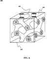
- FIG. 1Bdepicts a charge-splitting network architecture that may be used according to an embodiment of the present invention.
- FIG. 2depicts an example of a schematic of a device structure for a photovoltaic cell according to an embodiment of the present invention.
- FIG. 3depicts a flow diagram illustrating an example of a method for making a photovoltaic device of the type shown in FIG. 2 according to an embodiment of the present invention
- FIGS. 4A-4Fdepict a series of schematic diagrams illustrating the fabrication of a photovoltaic cell according to the flow diagram of FIG. 3 .
- FIG. 5depicts a ternary phase diagram representing the synthesis of a variety of architectures within a porous film.
- FIG. 6depicts an isometric close-up view of a portion of possible a porous film structure.
- FIG. 7depicts a graph of pore area vs. pore diameter for F127 templated polysiloxane porous film.
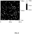
- FIG. 8depicts an atomic force micrograph of an example of a P123 surfactant-templated porous film suitable for use with embodiments of the present invention.
- FIG. 9Adepicts a plan view schematic diagram of a solar power generation system according to an embodiment of the present invention.
- FIG. 9Bdepicts a side-view cross-sectional schematic diagram of a portion of the solar power generation of FIG. 9A taken along line B-B.
- a conventional charge-splitting junction 100is a flat plane, with a low interfacial surface area between a hole-transporting layer 101 and an electron-transporting layer 102 .
- the junction 100has only a modest potential for harvesting excitons.
- the interfacial surface area between the hole- and electron-accepting materialsshould be reachable for excitons. According to an embodiment of the present invention, this can be achieved as shown in FIG. 1B through the creation of a three-dimensional nanoscale charge-splitting network. 110 .
- the charge-splitting network 110has interpenetrating regions with complementary charge-transfer properties, e.g., an electron-transporting material 111 and hole-transporting material 112 , that alternate in a substantially uniform fashion on a scale less than or equal to the exciton path length.
- the charge-splitting network 110is shown in simplified form for the sake of clarity. One possible variation, among others, of a configuration of a charge-splitting network 110 is shown in FIG. 6 .
- the charge-splitting network 110may be in the form of a porous nano-architected film having interconnected pores filled with a pore-filling material, wherein the porous nano-architected film and pore filling material have complementary charge-accepting properties.
- the porous nano-architected filmmay contain regularly spaced pores roughly 1 nm to 100 nm (more preferably 2 nm to 50 nm) in diameter where neighboring pores are between about 1 nm and about 100 nm (more preferably 2 nm to 50 nm) apart measured, e.g., from nearest edge to nearest edge.
- the poresare preferably interconnected with each other and accessible from any underlying layer and/or overlying layer.
- Such a porous nano-architected filmmay be a surfactant templated porous film.
- One approach to construct such a surfactant-templated porous filmis to use sol-gel based self-assembly of porous nanofilms to construct a 2-50 nm scale, solid-state charge-splitting network for solar cells.
- an optoelectronic deviceincludes (1) a low-cost, highly reproducible porous nano-architected film having interconnected pores filled with (2) a pore-filling material having complementary charge-transfer properties with respect to the porous nano-architected film.
- the pore-filling materialfills pores in the surfactant templated porous film to create an interpenetrating, nanoscale charge-splitting and transporting network for optoelectronic devices such as photovoltaic cells.
- the charge transfer properties of the porous film and pore filling materialmay be reversed, i.e., the porous film may be a hole acceptor with respect to the pore-filling material, which is an electron acceptor with respect to the porous nano-architected film.
- the porous filmmay be a hole acceptor with respect to the pore-filling material, which is an electron acceptor with respect to the porous nano-architected film.
- Such an optoelectronic devicemay be a photovoltaic device, such as a solar cell.
- the optoelectronic devicemay be a radiation-emitting device, such as an LED, laser, etc.
- FIG. 2depicts an example of a device structure for an optoelectronic device 200 according to an embodiment of the present invention.
- the photovoltaic cell 200generally includes a first electrode 202 , a charge-transport film 204 , a charge-splitting network 205 having an electron-accepting surfactant-templated porous film 206 and a hole-accepting pore-filling material 208 , and a second electrode 210 .
- the cell 200may optionally be protected by encapsulants 212 , 214 .
- a first optional interface layer 203may be disposed between the charge transport layer 204 and the first electrode to improve charge injection into the first electrode.
- the interface layer 203may also improve mechanical properties such as flexibility and resistance to short circuits.
- a similar second optional interface layer 209may be disposed between the pore-filling material 208 and the second electrode 210 .
- the first electrode 202which may serve as a base for the device 200 , may be in the form of a commercially available sheet material such as such as C- or Cu-coated Steel Foil.
- the charge transport film 204 and surfactant-templated porous film 206may both be solgel based and may both be composed of the same material, e.g., an electron-accepting material such as Titania (TiO 2 ) zinc oxide (ZnO 2 ), zirconium oxide, lanthanum oxide, niobium oxide, tungsten oxide, strontium oxide, calcium/titanium oxide, sodium titanate, potassium niobate.
- the charge-transport film 204may be made from different materials.
- the material used in the surfactant-templated porous film 206 and/or charge transport film 204may be altered to optimize its radiation absorption and/or charge transport properties, e.g., through carbon or hydrogen doping.
- the charge-transport film 204provides electrical contact between the surfactant-templated porous film 206 and the substrate electrode 202 .
- the charge transport film 204may be an electron-accepting sol-gel based non-porous Titania film.
- the nano-architected surfactant-templated porous film 206contains substantially uniformly distributed, e.g., regularly spaced, pores roughly 1 nm to 100 nm in diameter and more preferably, about 5 nm to about 15 nm in diameter. In general, neighboring pores are between about 1 nm and about 100 nm apart measured, e.g., from nearest edge to nearest edge. More preferably, the pores are between about 5 nm apart and 15 nm apart, edge to edge. Where organic semiconductors are used for either the surfactant-templated porous film 206 or the pore-filling material 208 , it is desirable for the size and spacing of the pores to be on the order of the exciton diffusion length in the respective organic semiconducting material. The substantially uniform distribution of the pores enhances the overall conversion efficiency of the photovoltaic cell 200 .
- the charge-splitting network 205is shown in simplified form for the sake of clarity. Although the pores in the charge-splitting network 205 may be aligned substantially parallel to each other as shown in FIG. 2 , the pores are preferably interconnected and accessible from both neighboring layers, e.g. electrodes 202 , 210 or interface layers 203 , 209 .
- One possible variation, among others, of a possible configuration of the pores in a charge-splitting networkis shown in FIG. 6 .
- the pore-filling material 208fills the pores in the surfactant-templated porous film 206 .
- the pore-filling material 208has complementary charge-accepting properties with respect to the surfactant-templated porous film 206 .
- the charge-transport film 204inhibits or prevents direct contact between the pore-filling material 208 and the substrate electrode 202 .
- the pore-filling material 208may cover the surfactant-templated porous film 206 in such a way as to inhibit direct contact between the surfactant-templated porous film 206 and the second electrode 210 .
- the surfactant-templated porous filmmay be made from an electron-accepting material, e.g., Titania
- the pore filling material 208may be a semiconducting, e.g., hole-accepting, organic material.
- suitable semiconducting organic materialsinclude conjugated polymers such as poly(phenylene) and derivatives thereof, poly(phenylene vinylene) and derivatives thereof (e.g., poly(2-methoxy-5-(2-ethyl-hexyloxy)-1,4-phenylene vinylene (MEH-PPV), poly(para-phenylene vinylene), (PPV)), poly(thiophene) and derivatives thereof (e.g., poly(3-octylthiophene-2,5,-diyl), regioregular, poly(3-octylthiophene-2,5,-diyl), regiorandom, Poly(3-hexylthiophene-2,5-diyl), regioregular, poly(3-hexylthiophene-2,5-diyl), regiorandom), poly(thienylenevinylene) and derivatives thereof, and poly(isothianaphthen
- suitable semiconducting polymersinclude organometallic polymers, polymers containing perylene units, poly(squaraines) and their derivatives.
- suitable semiconducting pore-filling materialsinclude organic pigments or dyes, azo-dyes having azo chromofores (—N ⁇ N—) linking aromatic groups, phthalocyanines including metal-free phthalocyanine; (HPc), perylenes, naphthalocyanines, squaraines, merocyanines and their respective derivatives, poly(silanes), poly(germinates), 2,9-Di(pent-3-yl)-anthra[2,1,9-def:6,5,10-d′e′f]diisoquinoline-1,3,8,10-tetrone, and 2,9-Bis-(1-hexyl-hept-1-yl)-anthra[2,1,9-def:6,5,10-d′e′f]diisoquinoline-1,3,8,10
- the pore-filling materialmay be a hole-accepting inorganic material such as copper oxide.
- the pore-filling material 208may be a combination of two or more compounds, e.g., solubilized buckminsterfullerene (C 60 ) and/or a dye, such as perylene and/or a polythiophene derivative.
- solubilized buckminsterfullereneC 60
- a dyesuch as perylene and/or a polythiophene derivative.
- the combination of the electron-accepting surfactant-templated porous film 206 and the hole-accepting pore-filling material 208creates a nanoscale, high-interfacial area charge-splitting network 205 .
- the second electrode 210provides an electrical connection to the pore-filling hole-accepting material 208 filling the pores.
- the substrate electrode 202 , the second electrode 210 or both electrodes 202 , 210are made from a material that transmits radiation of interest to the photovoltaic process that takes place within the cell 200 .
- suitable transparent conducting materials for the electrodes 202 , 210include doped tin oxide (SnO 2 ), e.g., fluorinated tin oxide F:SnO 2 , and indium-tin oxide (ITO).
- the optional interface layers 203 , 209may be made from conducting polymers, such as PEDOT or polyaniline.
- the interface layers 203 , 209may include a material, such as lithium fluoride (LiF) that improves charge injection into the electrodes 202 , 210 or smoothes out the surface roughness of the electrodes 202 , 210 .
- LiFlithium fluoride
- the optional encapsulants 212 , 214protect the cell 200 from the surrounding environment.
- suitable encapsulant materialsinclude one or more layers of polyethylene terephthalate (PET), and Mylar. Ethylene vinyl acetate (EVA) may be used in either case in conjunction with the other encapsulant.
- PETpolyethylene terephthalate
- EVAEthylene vinyl acetate
- the encapsulants 212 , 214may also include nitrides, oxides, oxynitrides or other inorganic materials that protect against exposure to water or air.
- the encapsulants 212 , 214may also absorb UV-light to protect organic materials disposed between the encapsulants 212 , 214 .
- the surfactant-templated porous film 206may be made from metal oxides, other than TiO 2 , or other semiconducting compounds that are capable of accepting electrons from the pore-filling material 208 and transporting the electrons.
- the surfactant-templated porous film 206may be made from metal oxides or other semiconductor compounds (e.g., conjugated polymers or dyes) that are hole-acceptors with respect to the pore-filling material 208 .
- metal oxides or other semiconductor compoundse.g., conjugated polymers or dyes
- CuOcopper oxide
- the pore-filling material 208would be an electron accepting material with respect to the material of the surfactant-templated porous film 206 .
- Charge-splitting networks of the types described above and optoelectronic devices of the type depicted in FIG. 2may be manufactured in accordance with an inventive method.
- An example of an embodiment of such a methodis 300 illustrated by the flow diagram of FIG. 3 and the series of schematic diagrams shown in FIGS. 4A-4F .
- the method 300may begin at 301 by optionally forming a first interface layer 403 on a first electrode 402 .
- an optional first charge-transport film 404may be formed on either the first electrode 402 or the first interface layer 403 as shown in FIG. 4A .
- a commercially available sheet materialsuch as such as C- or Cu-coated Steel Foil may be used as the substrate electrode 402 .
- the first charge-transport film 404may be a sol-gel based non-porous Titania (TiO 2 ) film.
- the non-porous TiO 2 filmmay be formed, e.g., using web-coating, dip-coating, spin-coating or spray-coating based deposition.
- a porous nano-architected filmsuch as a surfactant-templated film 406 , having pores 407 is formed on the charge-transport layer 404 as shown in FIG. 4B .
- the configuration of the pores 407is shown in simplified form for the sake of clarity. Although the pores 407 may be aligned substantially parallel to each other as shown in FIGS. 4B-4F , the pores 407 are preferably interconnected and accessible from both neighboring layers, e.g. electrodes or interface layers.
- FIG. 6One example, among others, of a possible configuration of the pores 407 is shown in FIG. 6 .
- the charge transport film 404 and surfactant-templated film 406may be made from any suitable material, including those described above with respect to the porous film 206 of FIG. 2 .
- the surfactant-templated film 406may be a made using a variety of surfactant temptation techniques such as evaporation induced self-assembly, etc.
- the surfactant-templated film 406may be formed, e.g. by web-coating, dip-coating, spin-coating or spray coating based deposition. By appropriate choice of the coating parameters, the surfactant-templated porous film 406 can be formed such that the pores 407 are roughly 2 nm to 100 nm in diameter and neighboring pores are between about 2 nm and about 100 nm apart.
- the surfactant-templated porous film 406is dried and, at 306 , the pores 407 are then filled with a pore-filling material 408 , as shown in FIG. 4C .
- the pore-filling material 408has complementary charge-accepting properties with respect to the surfactant-templated porous film 406 .
- the pore-filling material 408may be made of the materials described above the pore-filling material 208 of FIG. 2 .
- the surfactant-templated porous film 406may be made of Titania
- the pore-filling material 408may be an organic material, such as polythiophene, or an inorganic material, such as copper oxide.
- a second charge-transport film 409e.g., polythiophene may optionally be applied to the exposed surface of the pore-filling material 408 .
- the charge transport filmmay be made of any of the materials suitable for the pore-filling material 408 , e.g., as described above.
- the pore-filling material 408is then put in electrical contact with second electrode 410 , e.g. via the second charge-transport film 409 .
- the substrate 402 , porous film 406 , pore filling material, etc.may comprise one section 401 of a photovoltaic device.
- a second section 415may be built using a commercially-available sheet material 412 such as Mylar (Polyethylene Terephthalate, PET) as a transparent substrate.
- the sheet material 412may be coated with a transparent conducting material (e.g. a layer of tin oxide or indium tin oxide) to form the electrode 410 .
- An optional second interface layer 413may be applied to the second electrode 410
- An optional layer of charge-transport material 411such as polythiophene may be applied to the transparent second electrode 410 or the second interface layer 413 to complete the second section 415 .
- the first and second sections 401 , 415may then be laminated together at the homo-junction (dashed lines) between the pore-filling material layer 408 and the charge transport material layer 409 , as shown in FIG. 4E .
- the resulting devicemay be encapsulated.
- an encapsulant layer 414may cover the exposed surface of the substrate electrode 402 as shown in FIG. 4F .
- the substrate electrode 402may be mounted to the encapsulant layer 414 prior to forming non porous film 404 or the porous film 406 .
- the sheet material 412also may be used as an encapsulant layer.
- the key steps in the method 300are forming the surfactant-templated porous film ( 304 ) and filling the pores in the porous film with pore-filling material ( 306 ). Some approaches to accomplishing these two steps along with approaches to other steps in the method 300 are discussed in detail below.
- step 304 if FIG. 3there are several approaches to forming the porous nano-architected film described above.
- One such approachinvolves templated growth of inorganic or hybrid networks, e.g., by surfactant temptation.
- surfactant-templation techniques for producing porous filmsare described, e.g., by Brinker, et al in U.S. Pat. No. 6,270,846, the disclosures of which are incorporated herein by reference.
- One particular surfactant-templation approachutilizes evaporation-induced self-assembly (EISA) to form a meso-organized liquid-crystal template.
- EISAevaporation-induced self-assembly
- Pore diameter and pore spacingmay be adjusted by (1) choice of surfactant, (2) concentration of surfactant, (3) the use of block co-polymers, (4) temperature, (5) humidity level, (6) deposition procedure and speed, or some combination of two or more of (1), (2), (3), (4), (5) and (6).
- FIG. 5depicts a ternary phase diagram representing the synthesis of a variety of architectures within a porous film.
- the structure circled in FIG. 5depicts a simplified and somewhat idealized desirable morphology for the porous film.
- FIG. 6depicts a portion of a surfactant-templated porous film 600 .
- the film 600has numerous pores 601 that are interconnected with each other. Furthermore, the pores 601 provide a continuous path, through one or more pores, between a first surface 602 and a second surface 603 . The path through the pores 601 provides access to the pores from a layer overlying or a layer underlying the surfactant-templated porous film 600 .
- chargeshave a path to migrate through the pore filling material from the overlying layer to the underlying layer and/or vice versa.
- Porous silicadoes not have the appropriate electron-accepting properties required for the charge-splitting network layer 405 in an optoelectronic device such as a solar cell.
- a similar sol-gel based synthetic approachmay be used to produce, e.g., porous Titania or other metal oxide films.
- TiO 2Titania absorbs light from the near-ultraviolet region of the spectrum, and the material has relatively high charge mobility.
- Titaniadoes have the proper electronic properties for effective charge-splitting.
- Titaniais widely available and relatively inexpensive.
- Titania-based porous oxideby evaporation-induced self-assembly using a sol-gel technique, the higher reactivity of the titanium toward condensation (relative to silicon) must be controlled during the self-assembly process by the addition of any of a variety of stabilizing agents and hydrolysis-condensation inhibitors such as hydrogen peroxide, HCl, or triethanolamine.
- stabilizing agents and hydrolysis-condensation inhibitorssuch as hydrogen peroxide, HCl, or triethanolamine.
- the alkoxide, surfactant, condensation inhibitor, water and ethanolmay be mixed in molar ratios of about 1:0.1:1.4:17:20 respectively.
- Incubation temperature, ramp rate and total incubation timemay be varied to optimize the properties of the film.
- the initial surfactant concentrationscan be well below the critical micelle concentration (cmc), so the starting sols can have mesoscale homogeneity.
- a substratee.g., the first electrode 402 (e.g., C- or Cu-coated steel foil sheet)
- the first electrode 402e.g., C- or Cu-coated steel foil sheet
- preferential ethanol evaporationconcentrates the sol in water, non-volatile surfactant, and the titanium isopropoxide component thereby forming the surfactant-templated porous film.
- the progressively increasing concentration of surfactantdrives the self-assembly of metal-alkoxide surfactant micelles and their further organization into liquid-crystalline mesophases.
- the highly-ordered structure of the resulting liquid crystallitescan be permanently fixed through exposure to heat.
- the surfactant templatescan be selectively removed by annealing the surfactant templated porous film at a temperature ( ⁇ 250° C.) that is sufficient to decompose the surfactant molecules while remaining within the thermal stability range of the underlying C- or Cu-coated steel foil substrate ( ⁇ 1000° C.).
- annealingis required to fix the titania-oxygen matrix.
- This processing stepcovalently cross-links the Titania molecules to one another and to the surface into a fixed matrix.
- the processrequires an elevated temperature to drive the reaction in which the molecules are condensed into a cross-linked matrix with the loss of solvent or water.
- An annealing temperature of 250° C.is preferable as this temperature serves both to covalently cross-link the matrix and to pyrolyze the surfactant out of the matrix within a relatively short time.
- any remaining surfactantis removed by soaking the substrate in ethanol or another appropriate solvent.
- heating the surfactant templated porous film tomay anneal the Titania film and promotes the crystalline, anatase phase of the Titania, leading to a material with high electron mobility.
- the filmmay be annealed at 450 C. for 30 minutes. Alternatively, the film may be annealed for a shorter time at a higher temperature or for a longer time at a lower temperature.
- the annealingmay occur before the deposition of any hole-accepting material such as polythiophene into porous film (step 306 discussed below), as it is this initial step that creates the porous structure.
- any hole-accepting materialsuch as polythiophene into porous film (step 306 discussed below)
- the polymer to be deposited in a later stepwill not be affected by the annealing of the porous Titania film in this prior step.
- porous film 406For photovoltaic applications, it is desirable to create uniform films with regularly spaced pores having diameters of between about 1 nm and about 50 nm diameters, most preferably about 4 to 10 nm.
- the properties of the porous film 406e.g., pore size and surface area, may be confirmed by N 2 gas adsorption isotherms. Such isotherms may be obtained, e.g., at ⁇ 196° C. using a Beckman Coulter SA 3100 Surface Analyzer. Gas adsorption is considered an accurate method for determining surface area and pore size in the 2-200 nm range.
- inert gas molecules(N 2 ) are physisorbed onto the surface at a constant temperature, and the amount of gas adsorbed as a function of pressure is recorded as the adsorption isotherm.
- Monolayer formation on the sample by N 2 adsorbateoccurs due to favorable adsorbate-adsorbent energies and enables BET (Brunauer, Emmett, Teller) surface area calculation.
- Multilayer formationoccurs preferentially in the pores as a result of capillary adsorbate-adsorbate condensation and enables pore volume/size determination prior to bulk adsorbate-adsorbate interaction and condensation.
- FIG. 7shows data depicting the distribution of pore sizes in porous films created using the protocol described above.
- the graph in FIG. 7plots pore area vs. pore diameter for a F127 templated polysiloxane porous film. Solutions containing F127 surfactant and polysiloxane were dropcast, dried, and annealed at 400° C. for two hours. A porous matrix covering a lateral surface area of 78.5 cm 2 was scraped off and placed in a sample chamber for surface analysis. Data was acquired using a Beckman Coulter SA 3100 surface analyzer using liquid nitrogen; samples were analyzed using the BET and BJH algorithms. A narrow distribution of pore sizes clustered around 6 nm shows that the pore structure is relatively uniform within the film, and that this structure can be successfully measured using N 2 adsorption isotherms.
- Atomic Force Microcopycan be used to directly measure the sizes, orientations, and distributions of the pores in the porous film 306 , and to monitor the two-dimensional orientation of both inorganic and organic crystals, to characterize the surface roughness data of all films including the scratches and other defects.
- FIG. 8depicts an atomic force micrograph of an example of a surfactant-templated porous film manufactured using techniques of the type described above.
- a porous film of Titaniawas formed on a F:SnO 2 coated glass substrate using a sol mixture containing titanium ethoxide (an alkoxide), Pluronic P123 as a surfactant (available from BASF of Ludwigshafen, Germany), HCl as a condensation inhibitor, water and ethanol
- titanium tetraisopropoxidemay be used as the alkoxide and/or indium tin oxide (ITO) coated glass may be used as the substrate.
- the initial sol mixturewas prepared by refluxing titanium ethoxide, ethanol, water and an acid, such as HCl, at approximately 60° C.
- the molar ratios of the P123 surfactant, HCl, ethanol and watermay be in the following ranges with respect to titanium in the alkoxide:
- the solwas cooled to room temperature and the surfactant p123 was added in amounts ranging from 0.6 g to 1.2 g.
- the polymer, polypropylene oxide (PPO)was also added in amounts ranging from approximately 0 g to 1.2 g, were added to 5 mL of the sol, along with 0.8 mL of 1N HCl.
- the solwas filtered and a thin film was prepared from this solution by dip-coating onto the glass substrate. Prior to dip-coating, the substrate was cleaned by sequential washing in (i) acetone, then (ii) methanol, then (iii) isopropyl alcohol (IPA).
- IPAisopropyl alcohol
- surfactant-stabilized polypropylene microemulsionsincorporated into a surfactant-templated Titania material.
- the as-coated filmswere heated to approximately 400 to 450° C. for approximately 3 hours to remove the surfactant and polypropylene oxide templates. During part of this phase, the temperature was ramped up at between about 0.5° C./min and about 5° C./min from room temperature up to about 400° C.
- the resulting surfactant-templated filmhas pores about 9 nm to 13 nm in diameter, with the pores spaced about 10 nm to 17 nm apart.
- the pores 407 within the porous film 406are substantially filled with a pore-filling material 408 such as polythiophene or any of the other materials described above with respect to pore-filling material 208 .
- a nanometer-scale charge-splitting network layer 405can be formed to efficiently harvest excitons within the solar cell.
- the term “substantially filled”generally means that the pore-filling material 408 fills a significant volume of a sufficient percentage of the pores 407 . It is often desirable to completely fill at least some of the pores 407 with the pore-filling material 408 . In general, the larger the percentage of completely filled pores the better the performance of the resulting photovoltaic cell device.
- porous thin films with pores ranging from 4-10 m in diametermay be filled with a semiconducting, pore-filling material 408 such as the polymer poly 3-hexylthiophene (P3HT).
- P3HTis soluble in common organic solvents, and is an optically absorbent material between 400 and 700 nm, with a high hole mobility.
- One approach to filling the pores 407 of the porous film 406uses polymer in solution and an infiltration temperature of about 200° C. for about 30 minutes.
- Experiments in which porous Titania films have had their pores filledshow that it is possible for polymer material to enter into a pore and to fill the majority (>80%) of the pore volume. Should it be difficult for the pore volume to be entirely filled, the charge separation can still function within the resulting photovoltaic cell.
- the charge splitting network layer 405will have a very high interfacial surface area for highly efficient exciton splitting, while for the incompletely filled pores, the device will nevertheless still function as a single-layer optoelectronic or photovoltaic device. In both circumstances, excitons can be split, and the device can produce electric power. By maximizing the number of pores that are filled, the exciton harvesting efficiency may also be maximized.
- Pore filling and pore compositionmay be tested with absorption measurements and XPS depth profiling.
- XPSinvolves irradiating a solid in vacuum with mono-energetic soft X-rays and analyzing the energy of electrons emitted as a result.
- the electron energy spectrummay be obtained as a plot of the number of detected electrons per energy interval versus their binding energy. Each element has a unique spectrum, and so the spectrum from a mixture of elements is approximately the sum of the peaks of the individual constituents. Since the mean free path of electrons in solids is very short, the electrons detected by XPS mostly originate from only the top few atomic layers, making XPS a surface-sensitive technique.
- the pores 407 in the porous layer 406may be filled with a polymer as the pore-filling material 408 .
- the pores 407may be filled with a conducting, hole-accepting monomer material, which may be polymerized after monomer deposition within the pores 407 .
- the pores 407may be filled with an inorganic hole-accepting material such as Copper Oxide or other metal oxides, e.g., using electrodeposition.
- electrodeposit a variety of metalsincluding Pt, Cu, and Al
- ITO- or SnO 2 -coated glass, Mylarand a variety of other plastic substrates.
- the filled porous film 406may then be coated with a layer of hole-accepting material 409 .
- the layer of hole-accepting material 409coats the charge splitting network layer 405 .
- Any suitable coating techniquemay be used, e.g., dip coating, web coating, spin coating, spray coating, and the like.
- the layer of hole-accepting material 409may be made from a solution containing the same material 408 just used to fill the pores 407 .
- the pore-filling material 408 and the layer of hole-accepting material 409may both be made from a polymeric conductor, such as P3HT.
- the pore-filling material 408 and layer of hole-accepting material 409may be made from different materials. Measurement of uniform surface features by high-magnification optical microscopy may serve as a quality control check for this task.
- the hole accepting material 408to an electrode, e.g. via the layer of hole-accepting material 409 .
- FIGS. 4A-4Fit is possible to make such contact by building a photovoltaic cell device of the type shown in FIG. 2 in two sections and then joining the two sections together. Up to this point in the construction process (step 308 in FIG. 3 ), the first section 401 a photovoltaic cell device has been built.
- steps 310 and 312which are described in detail below, the second section 415 is built and the two sections are joined together to form a completed device of the type shown in FIG. 2 .
- the hole accepting electrode 410may be made from a foil comprised of C- or Cu-coated steel foil, which can also provide for mechanical strength.
- the foilcan be coated with a solution containing the same polymeric semiconductor (such as P3HT) used both to fill the pores 407 and to coat the filled charge-splitting and transporting network layer 405 .
- P3HTpolymeric semiconductor
- any suitable coating processmay be used, e.g., dip coating, web coating, spin coating, spray coating and the like. Lamination may also occur within the interface layers 403 , 413 or any other layer as long as a multilayer structure of the type depicted in FIG. 4E results.
- the first and second sections 401 , 415 of a photovoltaic cell devicemay be attached to each other by lamination at the homo-junction (indicated by the dashed line) between the conducting polymer material coating the hole-accepting electrode 410 and the same polymer material coating the charge-splitting network layer 405 .
- the homo-junctionindicated by the dashed line
- FIGS. 9A-9BAn example of such a power generation system 900 is depicted in FIGS. 9A-9B .
- the power system 900generally comprises an array 901 of photovoltaic cells 902 having features in common with those described above with respect to FIGS. 2 and 4 A- 4 F.
- one or more of the cells 902 in the array 901includes one or more charge-splitting networks 905 disposed between an electron-accepting electrode 904 and a hole-accepting electrode 906 .
- Each charge splitting network 905includes a porous film having uniformly distributed nanometer-scale pores that are filled with a pore-filling material.
- the porous film and the pore-filling materialhave complementary charge-accepting properties with respect to each other, i.e., one material acts an electron-acceptor with respect to the other material, which acts as a hole-acceptor.
- the electron-acceptorwould be in electrical contact with the electron-acceptor electrode 904 and the hole-acceptor material would be in electrical contact with the hole-acceptor electrode 906 .
- An interaction between radiation and the charge-splitting network 905generates an electrical voltage between the electron-accepting electrode 904 and the hole-accepting electrode 906 .
- the porous filmmay be an electron-accepting Titania-based surfactant templated film and the pore filling material may be a suitable hole-accepting material.
- two or more cellsmay be electrically connected in series.
- cells 902 , 902 A, and 902 Bare connected in series, with the hole-accepting electrode 906 of cell 902 connected to the electron-accepting electrode 904 A of cell 902 A and the hole accepting electrode 906 A of cell 902 A connected to the electron-accepting electrode 904 B of cell 902 B.
- interconnect of solar cellsmany of which can be applied to the device structure. For example, standard scribing/etching techniques as used by many thin-film manufacturers can be used.
- either the electron-accepting electrode or the hole-accepting electrodemay be separated by laser grooving, mechanical separation (mechanical grooving), or a separating line (e.g., ⁇ 0.5 mm wide) can be etched across a large area photovoltaic web using a macroscopic screen (no photolithography is required).
- a separating linee.g., ⁇ 0.5 mm wide
- the cells 902can be interconnected in series by overlapping the transparent electrodes (which can be similarly divided) with the bottom layer.
- Organic solar cellstypically generate higher voltages than most inorganic cell structures, resulting in individual cell voltages between 0.7 and 1.3 V, and thus these cells require fewer interconnects to obtain the higher aggregate voltages as desired in many applications.
- Conventional cellstend to generate only about 0.5 to 0.8V per cell; and, further, silicon-based cells are restricted to the common silicon wafer sizes so that they need to connect many cells in parallel to obtain high currents by covering a larger surface area.
- the systemmay optionally include an energy storage device 908 connected to the array 901 .
- the energy storage systemmay be in the form of one or more batteries or one or more electrolytic cells for producing hydrogen form water using electricity generated by the cells 902 in the array 901 .
- the cells 902may be configured to generate hydrogen from water directly using a radiation-driven electrolytic reaction.
- the storage device 908may include a storage tank for holding the hydrogen and/or a fuel cell for converting the energy stored in the hydrogen back to electric power on demand.
- the system 900may be scaled as a stand-alone for a commercial or residential facility.
- the systemmay include an optional DC-AC converter 910 so that electric power produced by the system 900 may be distributed over a conventional electric power grid. Because of the improved efficiency and lower manufacturing cost of photovoltaic cells of the type described herein the system 900 is potentially capable of producing electric power at a cost per kilowatt hour (kwh) competitive with conventional electric grid rates.
- Porous nano-architected films for charge-splitting networks or optoelectronic devicesmay alternatively be fabricated by such approaches as: (a) Intercalation and/or grafting of organic or polymeric molecules within a mineral lamellar network; (b) Synthesis by electrocrystallisation of hybrid molecular assemblies; (c) Impregnation of preformed inorganic gels; (d) Synthesis from heterofunctional metallic alkoxides or silsesquioxannes; (e) Synthesis of hybrid through the connection of well defined functional nanobuilding blocks; and (f) templated growth of inorganic or hybrid networks by using organic molecules and macromolecules other than surfactants, e.g., amines, alkyl ammonium ions, amphiphilic molecules, as structure directing agents.
- surfactantse.g., amines, alkyl ammonium ions, amphiphilic molecules, as structure directing agents.
- Suitable adjustment of the result effective parameters in these techniquesmay produce a nano-architected film having interconnected pores that are distributed in a substantially uniform fashion with neighboring pores separated by a distance of between about 1 nm and about 100 nm, wherein the pores have diameters of between about 1 nm and about 100 nm.
- the interconnected poresmay be accessible from an underlying layer and/or overlying layer (if any).
- the pores in a porous nano-architected produced by any of these techniquesmay be filled with a pore-filling material having complementary charge transfer properties as described above.
- Embodiments of the present inventionprovide a novel and useful optoelectronic devices, such as photovoltaic cell devices for use in electric power production as well as methods for the manufacture of such materials and power systems using such devices.
- the charge-splitting networks and photovoltaic cells described hereinare potentially less expensive to manufacture than conventional charge-splitting networks, optoelectronic devices and photovoltaic cells. It is to be understood that the above description is intended to be illustrative and not restrictive. Many embodiments and variations of the invention will become apparent to those of skill in the art upon review of this disclosure. Merely by way of example a wide variety of process times, reaction temperatures and other reaction conditions may be utilized, as well as a different ordering of certain processing steps. The scope of the invention should, therefore, be determined not with reference to the above description, but instead should be determined with reference to the appended claims along with the full scope of equivalents to which such claims are entitled.
Landscapes
- Physics & Mathematics (AREA)
- Electromagnetism (AREA)
- Chemical & Material Sciences (AREA)
- Inorganic Chemistry (AREA)
- Photovoltaic Devices (AREA)
- Hybrid Cells (AREA)
- Physical Deposition Of Substances That Are Components Of Semiconductor Devices (AREA)
Abstract
Description
- I. Glossary
- II. General Overview
- III. Solar Cell Device Architecture
- IV. Alternative Embodiments
- V. Conclusion
- Device: An assembly or sub-assembly having one or more layers of material.
- Semiconductor: As used herein, semiconductor generally refers to a material characterized by an electronic bandgap typically between about 0.5 eV and about 3.5 eV.
- Hole-Acceptor, Electron-Acceptor: In the case of semiconductor materials, hole-acceptor and electron-acceptor are relative terms for describing charge transfer between two materials. For two semiconductor materials wherein a first material has a valence band edge or highest occupied molecular orbital (HOMO) that is higher than the corresponding valence band edge or HOMO for a second material, and wherein the first material has a conduction band edge or lowest unoccupied molecular orbital (LUMO) that is higher than the corresponding conduction band edge or LUMO for the second material, the first material is a hole-acceptor with respect to the second material and the second material is an electron-acceptor with respect to the first material. A particular band edge or molecular orbital is said to be “higher” when it is closer the vacuum level.
- Complementary charge-transfer properties: As used herein, a first and second semiconductor material are said to have complementary charge-transfer properties with respect to each other when the first material is a hole-acceptor with respect to the second and the second is an electron-acceptor with respect to the first or vice versa.
- Nano-Architected Porous Film: As used herein “nano-architected porous film” generally refers to a film of material having features characterized by a width, or other characteristic dimension, on the order of several nanometers (10−9m) across. Nano-architected porous films may be produced by several techniques, including:
- (a) Intercalation and/or grafting of organic or polymeric molecules within a mineral lamellar network comprised of clays, phosphates, phosphonates, etc. The lamellar compounds serve as a network host which preserves the pre-established structural order. Organic molecules are then inserted or grafted into this pre-structured network (which is comprised of mineral(s)).
- (b) Synthesis by electrocrystallisation of hybrid molecular assemblies. This synthesis technique drives the construction of highly organized mineral networks with relatively long-range order that can be controlled and adjusted for electronic intermolecular transfer.
- (c) Impregnation of preformed inorganic gels. In an example of this technique, a silica xerogel can be formed by hydrolysis and polycondensation of silicon alkoxides with organic monomers (e.g. with monomers that are susceptible to polymerization within the porous gel structure). Methylmethacrylate (MMA) is an example of a suitable organic monomer and the inorganic-organic hybrid obtained after polymerization of the MMA has optical and mechanical properties often superior to the individual components.
- (d) Synthesis from heterofunctional metallic alkoxides or silsesquioxannes: Precursors of this kind have the formula RxM(OR′)n-xor 3(R′O)Si—R—Si(OR′)3, where R and R′ are either hydrogen (H) or any organic functional group, and M is a metal. Typically R and R′ involve oxygen, e.g., —O—R and —O—R′. M may be any transition metal, e.g., titanium, zinc, zirconium, copper, lanthanum, niobium, strontium, etc. The hydrolysis of alkoxy groups (OR′) followed by a condensation reaction will form the mineral network and the R groups will imprint in the network the organic function.
- (e) Synthesis of hybrid through the connection of well-defined functional nanobuilding Blocks. The pre-formatted species or building blocks could be in this case oxo-metallic clusters, nanoparticles (CdS, CdSe, . . . ), metallic or oxides colloids, organic molecules or oligomers. These blocks are functionalized during or after their synthesis with complementary species for tailoring the interface between organic and inorganic domains. A review of this strategy has been presented in Comments in Inorganic Chemistry20(4-6), 327-371 (1999), which is incorporated herein by reference.
- (f) Templated growth of inorganic or hybrid networks by using organic molecules and macromolecules as structure directing agents. In general, molecules like amines, alkyl ammonium ions, amphiphilic molecules or surfactants can be used as templates to build a structured mineral network. Materials of the zeolites families are among the most intensively investigated systems. Molecular and supramolecular interactions between template molecules (surfactants, amphiphilic block copolymers, organogelators, etc. . . . ) and the growing hybrid or metal-oxo based network permit the construction of complex hybrid hierarchical architectures.
- Surfactant Templation: In general, surfactant templation is a particular subcategory of templated growth. As used herein, surfactant templation refers an approach toward achieving pore size control of inorganic or organic frameworks, e.g., by using surfactants as templates to build a structured mineral network. Surfactant templation may be used to prepare a high-porosity surfactant-templated porous thin film. Surfactant temptation includes the sol-gel approach described below.
- Optoelectronic Device: A device that interacts with radiation and electric current. Such a device could be a radiation-emitting device, e.g. a light-emitting diode (LED) or laser, or a radiation absorbing device, e.g. a photodetector/counter, photovoltaic cell (solar cell) or radiation-driven electrolysis cell.
- Solar Cell: A photovoltaic device that interacts with radiation (often in the form of sunlight) impinging on the device to produce electric power or voltage.
- Organic Solar Cell: A type of solar cell wherein an active photoelectric layer is fabricated, either partly or entirely, using organic materials comprising, e.g., polymers, dyes, pigments (including mixtures) that are predominantly carbon based compounds. These materials may be insulating, conductive or semiconductive.
- Radiation: Energy which may be selectively applied including electromagnetic energy having a wavelength between 10−14and 104meters including, for example, gamma radiation, x-ray radiation, ultraviolet radiation, visible light, infrared radiation, microwave radiation and radio waves.
- Material: The term “material” is used herein to refer to solid-state compounds, extended solids, extended solutions, clusters of molecules or atoms, crystals, polymers, dyes, particularly including conjugated polymers and dyes.
- Inorganic Materials: Materials which do not contain carbon as a principal element. The oxides and sulphides of carbon and the metallic carbides are considered inorganic materials. Examples of inorganic compounds include, but are not restricted to, the following:
- (a) Intermetallics (or Intermediate Constituents): Intermetallic compounds constitute a unique class of metallic materials that form long-range ordered crystal structures below a critical temperature. Such materials form when atoms of two metals combine in certain proportions to form crystals with a different structure from that of either of the two metals (e.g., NiAl, CrBe2, CuZn, etc.).
- (b) Metal Alloys: A substance having metallic properties and which is composed of a mixture of two or more chemical elements of which at least one is a metal.
- (c) Magnetic Alloys: An alloy exhibiting ferromagnetism such as silicon iron, but also iron-nickel alloys, which may contain small amounts of any of a number of other elements (e.g., copper, aluminum, chromium, molybdenum, vanadium, etc.), and iron-cobalt alloys.
- (d) Inorganic polymers such as polysilanes or other non-carbon based polymers or monomers.
- (e) Ceramics: Typically, a ceramic is a metal oxide, boride, carbide, nitride, or a mixture of such materials. Examples of such materials include, among others, alumina, zirconia, Titania (TiO2) silicon carbide, aluminum nitride, silicon nitride
- Organic Materials: Compounds, which principally consist of carbon and hydrogen, with or without oxygen, nitrogen or other elements, except those in which carbon does not play a critical role (e.g., carbonate salts). Examples of organic materials that can be synthesized using the methods of the present invention include, but are not restricted to, the following:
- (a) Organic Dyes and pigments such as derivatives of perylenes, phthalocyanines, merocyanines, terylenes, squaraines, ruthenium, and pentacene.
- (b) Polymers: Materials consisting of large macromolecules composed of many repeating units. Examples of such repeating units include, e.g., dyes or pigments. Polymers can be natural or synthetic, cross-linked or non-crosslinked, and they may be homopolymers, copolymers, or higher-ordered polymers (e.g., terpolymers, etc.). Examples of polymers include, but are not limited to, the following: polyurethanes, polyesters, polycarbonates, polyethyleneimines, polyacetates, polystyrenes, polyamides, polyanilines, polyacetylenes, polypyrroles, conjugated polymers, (e.g., semiconductive polymers such as poly(pheylene), polyphenylvinylene, poly(isothianaphthene), polythiophene, poly(thienylenevinylene), polyfluorenes, polyparaphenylene, poly(isothianaphthene), poly(squaraine), and polymers containing C60or dyes such as perylenes or phthalocyanines) or conductive polymers such as doped PEDOT (Baytron) or polyaniline or polyacetylene. These may be synthesized or grafted onto one another using either classical organic chemistry techniques or using enzymes to catalyze specific reactions.
- [Surfactant]/[alkoxide]: a molar ratio ranging from about 1×10⁻⁷to about 0.1
- [Ethanol]/[alkoxide]: a molar ratio ranging from about 3 to about 20
- [Condensation Inhibitor]/[alkoxide]: a molar ranging ratio from about 1.5×10⁻⁵to about 5.0
- [water]/[alkoxide]: a molar ratio ranging from about 1 to about 20.
- [P123]/[Ti] a molar ratio ranging from about 1×10⁻⁷to about 1×10⁻⁵
- [Ethanol]/[Ti] a molar ratio ranging from about 10 to about 20
- [HCl]/[Ti] a molar ratio ranging from about 0.5 to about 5
- [H2O]/[Ti] a molar ratio ranging from about 1 to about 10
Claims (32)
Priority Applications (11)
| Application Number | Priority Date | Filing Date | Title |
|---|---|---|---|
| US10/290,119US7291782B2 (en) | 2002-06-22 | 2002-11-05 | Optoelectronic device and fabrication method |
| US10/303,665US7253017B1 (en) | 2002-06-22 | 2002-11-22 | Molding technique for fabrication of optoelectronic devices |
| US10/338,079US7594982B1 (en) | 2002-06-22 | 2003-01-06 | Nanostructured transparent conducting electrode |
| US10/443,456US6946597B2 (en) | 2002-06-22 | 2003-05-21 | Photovoltaic devices fabricated by growth from porous template |
| AU2003301934AAU2003301934A1 (en) | 2002-06-22 | 2003-06-17 | Photovoltaic devices fabricated by growth from porous template |
| DE10392830TDE10392830T5 (en) | 2002-06-22 | 2003-06-17 | Photovoltaic systems that are produced by growing from a porous template |
| PCT/US2003/019173WO2004044948A2 (en) | 2002-06-22 | 2003-06-17 | Photovoltaic devices fabricated by growth from porous template |
| AU2003291756AAU2003291756A1 (en) | 2002-11-05 | 2003-11-04 | Photovoltaic devices fabricated by growth from porous template |
| PCT/US2003/035147WO2004042432A2 (en) | 2002-11-05 | 2003-11-04 | Photovoltaic devices fabricated by growth from porous template |
| US11/375,413US20060174934A1 (en) | 2002-11-05 | 2006-03-13 | Optoelectronic device and frabrication method |
| US13/626,919US20130020557A1 (en) | 2002-06-22 | 2012-09-26 | Nanostructured transparent conducting electrode |
Applications Claiming Priority (2)
| Application Number | Priority Date | Filing Date | Title |
|---|---|---|---|
| US39090402P | 2002-06-22 | 2002-06-22 | |
| US10/290,119US7291782B2 (en) | 2002-06-22 | 2002-11-05 | Optoelectronic device and fabrication method |
Related Parent Applications (1)
| Application Number | Title | Priority Date | Filing Date |
|---|---|---|---|
| US10/303,665Continuation-In-PartUS7253017B1 (en) | 2002-06-22 | 2002-11-22 | Molding technique for fabrication of optoelectronic devices |
Related Child Applications (5)
| Application Number | Title | Priority Date | Filing Date |
|---|---|---|---|
| US10/303,665Continuation-In-PartUS7253017B1 (en) | 2002-06-22 | 2002-11-22 | Molding technique for fabrication of optoelectronic devices |
| US10/330,665Continuation-In-PartUS6732507B1 (en) | 2002-12-30 | 2002-12-30 | NOx aftertreatment system and method for internal combustion engines |
| US10/338,079Continuation-In-PartUS7594982B1 (en) | 2002-06-22 | 2003-01-06 | Nanostructured transparent conducting electrode |
| US10/443,456Continuation-In-PartUS6946597B2 (en) | 2002-06-22 | 2003-05-21 | Photovoltaic devices fabricated by growth from porous template |
| US11/375,413ContinuationUS20060174934A1 (en) | 2002-11-05 | 2006-03-13 | Optoelectronic device and frabrication method |
Publications (3)
| Publication Number | Publication Date |
|---|---|
| US20040084080A1 US20040084080A1 (en) | 2004-05-06 |
| US20070181177A9 US20070181177A9 (en) | 2007-08-09 |
| US7291782B2true US7291782B2 (en) | 2007-11-06 |
Family
ID=32176137
Family Applications (2)
| Application Number | Title | Priority Date | Filing Date |
|---|---|---|---|
| US10/290,119Expired - Fee RelatedUS7291782B2 (en) | 2002-06-22 | 2002-11-05 | Optoelectronic device and fabrication method |
| US11/375,413AbandonedUS20060174934A1 (en) | 2002-11-05 | 2006-03-13 | Optoelectronic device and frabrication method |
Family Applications After (1)
| Application Number | Title | Priority Date | Filing Date |
|---|---|---|---|
| US11/375,413AbandonedUS20060174934A1 (en) | 2002-11-05 | 2006-03-13 | Optoelectronic device and frabrication method |
Country Status (3)
| Country | Link |
|---|---|
| US (2) | US7291782B2 (en) |
| AU (1) | AU2003291756A1 (en) |
| WO (1) | WO2004042432A2 (en) |
Cited By (62)
| Publication number | Priority date | Publication date | Assignee | Title |
|---|---|---|---|---|
| US20050098204A1 (en)* | 2003-05-21 | 2005-05-12 | Nanosolar, Inc. | Photovoltaic devices fabricated from nanostructured template |
| US20050098205A1 (en)* | 2003-05-21 | 2005-05-12 | Nanosolar, Inc. | Photovoltaic devices fabricated from insulating nanostructured template |
| US20050263503A1 (en)* | 2002-08-21 | 2005-12-01 | Brzesowsky Rudolf H | Method of breaking a brittle substrate |
| US20060174934A1 (en)* | 2002-11-05 | 2006-08-10 | Nanosolar, Inc. | Optoelectronic device and frabrication method |
| US20060234505A1 (en)* | 2003-12-18 | 2006-10-19 | Nippon Oil Corporation | Method for manufacturing nano-array electrode and photoelectric conversion device using same |
| US20070111368A1 (en)* | 2005-11-16 | 2007-05-17 | Sharp Laboratories Of America, Inc. | Photovoltaic structure with a conductive nanowire array electrode |
| US20080176030A1 (en)* | 2002-06-08 | 2008-07-24 | Fonash Stephen J | Lateral collection photovoltaics |
| US7511217B1 (en) | 2003-04-19 | 2009-03-31 | Nanosolar, Inc. | Inter facial architecture for nanostructured optoelectronic devices |
| US7589880B2 (en) | 2005-08-24 | 2009-09-15 | The Trustees Of Boston College | Apparatus and methods for manipulating light using nanoscale cometal structures |
| US7594982B1 (en) | 2002-06-22 | 2009-09-29 | Nanosolar, Inc. | Nanostructured transparent conducting electrode |
| US20090266418A1 (en)* | 2008-02-18 | 2009-10-29 | Board Of Regents, The University Of Texas System | Photovoltaic devices based on nanostructured polymer films molded from porous template |
| US20100051856A1 (en)* | 2008-08-26 | 2010-03-04 | Samsung Sdi Co., Ltd. | Porous anode active material, method of manufacturing the same, anode comprising the same, and lithium battery comprising the anode |
| US20100133093A1 (en)* | 2009-04-13 | 2010-06-03 | Mackie Neil M | Method for alkali doping of thin film photovoltaic materials |
| US20100166954A1 (en)* | 2003-04-29 | 2010-07-01 | Jacqueline Fidanza | Nanostructured Layer and Fabrication Methods |
| US7754964B2 (en) | 2005-08-24 | 2010-07-13 | The Trustees Of Boston College | Apparatus and methods for solar energy conversion using nanocoax structures |
| US20100212733A1 (en)* | 2009-02-20 | 2010-08-26 | Miasole | Protective layer for large-scale production of thin-film solar cells |
| US7785921B1 (en) | 2009-04-13 | 2010-08-31 | Miasole | Barrier for doped molybdenum targets |
| US20100258191A1 (en)* | 2009-04-13 | 2010-10-14 | Miasole | Method and apparatus for controllable sodium delivery for thin film photovoltaic materials |
| US20110024285A1 (en)* | 2009-07-30 | 2011-02-03 | Juliano Daniel R | Method for alkali doping of thin film photovoltaic materials |
| US20110023955A1 (en)* | 2007-06-26 | 2011-02-03 | Fonash Stephen J | Lateral collection photovoltaics |
| US7935558B1 (en) | 2010-10-19 | 2011-05-03 | Miasole | Sodium salt containing CIG targets, methods of making and methods of use thereof |
| US7943847B2 (en) | 2005-08-24 | 2011-05-17 | The Trustees Of Boston College | Apparatus and methods for solar energy conversion using nanoscale cometal structures |
| US20110162696A1 (en)* | 2010-01-05 | 2011-07-07 | Miasole | Photovoltaic materials with controllable zinc and sodium content and method of making thereof |
| US20110253205A1 (en)* | 2008-09-27 | 2011-10-20 | The Regents Of The University Of California | Nanoscale Solar Cell Configuration |
| US8048707B1 (en) | 2010-10-19 | 2011-11-01 | Miasole | Sulfur salt containing CIG targets, methods of making and methods of use thereof |
| WO2011062457A3 (en)* | 2009-11-23 | 2011-11-03 | 한양대학교 산학협력단 | Organic-inorganic hybrid solar cell and manufacturing method thereof |
| US20120028406A1 (en)* | 2007-04-25 | 2012-02-02 | James Harris | Hybrid photovoltaic cells and related methods |
| US8110738B2 (en) | 2009-02-20 | 2012-02-07 | Miasole | Protective layer for large-scale production of thin-film solar cells |
| US8418418B2 (en) | 2009-04-29 | 2013-04-16 | 3Form, Inc. | Architectural panels with organic photovoltaic interlayers and methods of forming the same |
| US8435825B2 (en)* | 2007-01-11 | 2013-05-07 | General Electric Company | Methods for fabrication of nanowall solar cells and optoelectronic devices |
| US20140041723A1 (en)* | 2011-06-14 | 2014-02-13 | Panasonic Corporation | Solar cell and method for fabricating the same |
| US20140053900A1 (en)* | 2012-01-11 | 2014-02-27 | Panasonic Corporation | Solar cell element |
| US8709335B1 (en) | 2009-10-20 | 2014-04-29 | Hanergy Holding Group Ltd. | Method of making a CIG target by cold spraying |
| US8709548B1 (en) | 2009-10-20 | 2014-04-29 | Hanergy Holding Group Ltd. | Method of making a CIG target by spray forming |
| US8933238B2 (en) | 2013-03-11 | 2015-01-13 | Saudi Basic Industries Corporation | Aryloxy-phthalocyanines of group III metals |
| US8994009B2 (en) | 2011-09-07 | 2015-03-31 | Semiconductor Energy Laboratory Co., Ltd. | Photoelectric conversion device |
| RU2548402C1 (en)* | 2013-12-17 | 2015-04-20 | Федеральное государственное бюджетное образовательное учреждение высшего профессионального образования Северо-Кавказский горно-металлургический институт (государственный технологический университет) (СКГМИ (ГТУ) | Method of producing aluminium oxide-based photoconverter |
| US9040710B2 (en) | 2013-03-11 | 2015-05-26 | Saudi Basic Industries Corporation | Aryloxy-phthalocyanines of group IV metals |
| US9159939B2 (en) | 2011-07-21 | 2015-10-13 | Semiconductor Energy Laboratory Co., Ltd. | Photoelectric conversion device |
| US9169548B1 (en) | 2010-10-19 | 2015-10-27 | Apollo Precision Fujian Limited | Photovoltaic cell with copper poor CIGS absorber layer and method of making thereof |
| US9847581B2 (en) | 2009-06-17 | 2017-12-19 | L. Pierre de Rochemont | Frequency-selective dipole antennas |
| US9882274B2 (en) | 2004-10-01 | 2018-01-30 | L. Pierre de Rochemont | Ceramic antenna module and methods of manufacture thereof |
| US10043921B1 (en) | 2011-12-21 | 2018-08-07 | Beijing Apollo Ding Rong Solar Technology Co., Ltd. | Photovoltaic cell with high efficiency cigs absorber layer with low minority carrier lifetime and method of making thereof |
| US10707526B2 (en) | 2015-03-27 | 2020-07-07 | New Dominion Enterprises Inc. | All-inorganic solvents for electrolytes |
| US10707531B1 (en) | 2016-09-27 | 2020-07-07 | New Dominion Enterprises Inc. | All-inorganic solvents for electrolytes |
| USD940149S1 (en) | 2017-06-08 | 2022-01-04 | Insulet Corporation | Display screen with a graphical user interface |
| USD977502S1 (en) | 2020-06-09 | 2023-02-07 | Insulet Corporation | Display screen with graphical user interface |
| US11857763B2 (en) | 2016-01-14 | 2024-01-02 | Insulet Corporation | Adjusting insulin delivery rates |
| US11865299B2 (en) | 2008-08-20 | 2024-01-09 | Insulet Corporation | Infusion pump systems and methods |
| US11929158B2 (en) | 2016-01-13 | 2024-03-12 | Insulet Corporation | User interface for diabetes management system |
| USD1020794S1 (en) | 2018-04-02 | 2024-04-02 | Bigfoot Biomedical, Inc. | Medication delivery device with icons |
| USD1024090S1 (en) | 2019-01-09 | 2024-04-23 | Bigfoot Biomedical, Inc. | Display screen or portion thereof with graphical user interface associated with insulin delivery |
| US11969579B2 (en) | 2017-01-13 | 2024-04-30 | Insulet Corporation | Insulin delivery methods, systems and devices |
| US12042630B2 (en) | 2017-01-13 | 2024-07-23 | Insulet Corporation | System and method for adjusting insulin delivery |
| US12064591B2 (en) | 2013-07-19 | 2024-08-20 | Insulet Corporation | Infusion pump system and method |
| US12076160B2 (en) | 2016-12-12 | 2024-09-03 | Insulet Corporation | Alarms and alerts for medication delivery devices and systems |
| US12097355B2 (en) | 2023-01-06 | 2024-09-24 | Insulet Corporation | Automatically or manually initiated meal bolus delivery with subsequent automatic safety constraint relaxation |
| US12106837B2 (en) | 2016-01-14 | 2024-10-01 | Insulet Corporation | Occlusion resolution in medication delivery devices, systems, and methods |
| US12318594B2 (en) | 2016-05-26 | 2025-06-03 | Insulet Corporation | On-body interlock for drug delivery device |
| US12318577B2 (en) | 2017-01-13 | 2025-06-03 | Insulet Corporation | System and method for adjusting insulin delivery |
| US12343502B2 (en) | 2017-01-13 | 2025-07-01 | Insulet Corporation | System and method for adjusting insulin delivery |
| US12383166B2 (en) | 2016-05-23 | 2025-08-12 | Insulet Corporation | Insulin delivery system and methods with risk-based set points |
Families Citing this family (171)
| Publication number | Priority date | Publication date | Assignee | Title |
|---|---|---|---|---|
| US6649824B1 (en)* | 1999-09-22 | 2003-11-18 | Canon Kabushiki Kaisha | Photoelectric conversion device and method of production thereof |
| SE0103740D0 (en)* | 2001-11-08 | 2001-11-08 | Forskarpatent I Vaest Ab | Photovoltaic element and production methods |
| US6919119B2 (en)* | 2000-05-30 | 2005-07-19 | The Penn State Research Foundation | Electronic and opto-electronic devices fabricated from nanostructured high surface to volume ratio thin films |
| DE60132450T2 (en)* | 2001-09-04 | 2008-04-17 | Sony Deutschland Gmbh | Solar cell and manufacturing method |
| WO2003043934A1 (en) | 2001-11-20 | 2003-05-30 | Wm. Marsh Rice University | Coated fullerenes, composites and dielectrics made therefrom |
| US7259324B2 (en)* | 2001-12-05 | 2007-08-21 | Konarka Technologies, Inc. | Photovoltaic solar cell |
| US8749054B2 (en) | 2010-06-24 | 2014-06-10 | L. Pierre de Rochemont | Semiconductor carrier with vertical power FET module |
| US20070251570A1 (en)* | 2002-03-29 | 2007-11-01 | Konarka Technologies, Inc. | Photovoltaic cells utilizing mesh electrodes |
| US6946597B2 (en)* | 2002-06-22 | 2005-09-20 | Nanosular, Inc. | Photovoltaic devices fabricated by growth from porous template |
| US7253017B1 (en)* | 2002-06-22 | 2007-08-07 | Nanosolar, Inc. | Molding technique for fabrication of optoelectronic devices |
| TW200425530A (en)* | 2002-09-05 | 2004-11-16 | Nanosys Inc | Nanostructure and nanocomposite based compositions and photovoltaic devices |
| WO2005000735A2 (en) | 2002-11-19 | 2005-01-06 | William Marsh Rice University | Method for creating a functional interface between a nanoparticle, nanotube or nanowire, and a biological molecule or system |
| AU2003295721A1 (en) | 2002-11-19 | 2004-06-15 | William Marsh Rice University | Fabrication of light emitting film coated fullerenes and their application for in-vivo light emission |
| US6969897B2 (en)* | 2002-12-10 | 2005-11-29 | Kim Ii John | Optoelectronic devices employing fibers for light collection and emission |
| DE10300521A1 (en)* | 2003-01-09 | 2004-07-22 | Siemens Ag | Organoresistive memory |
| WO2004086462A2 (en)* | 2003-03-24 | 2004-10-07 | Konarka Technologies, Inc. | Photovoltaic cell with mesh electrode |
| US6936761B2 (en)* | 2003-03-29 | 2005-08-30 | Nanosolar, Inc. | Transparent electrode, optoelectronic apparatus and devices |
| CN1813362A (en)* | 2003-06-26 | 2006-08-02 | 纳幕尔杜邦公司 | Method of forming a pattern of filled dielectric material on a substrate |
| JP2005032852A (en)* | 2003-07-09 | 2005-02-03 | Matsushita Electric Ind Co Ltd | Organic photoelectric conversion element |
| US20050098534A1 (en)* | 2003-11-12 | 2005-05-12 | Molecular Imprints, Inc. | Formation of conductive templates employing indium tin oxide |
| US7045205B1 (en) | 2004-02-19 | 2006-05-16 | Nanosolar, Inc. | Device based on coated nanoporous structure |
| US7115304B2 (en)* | 2004-02-19 | 2006-10-03 | Nanosolar, Inc. | High throughput surface treatment on coiled flexible substrates |
| US7663057B2 (en)* | 2004-02-19 | 2010-02-16 | Nanosolar, Inc. | Solution-based fabrication of photovoltaic cell |
| US8846141B1 (en) | 2004-02-19 | 2014-09-30 | Aeris Capital Sustainable Ip Ltd. | High-throughput printing of semiconductor precursor layer from microflake particles |
| US20080220984A1 (en)* | 2004-03-10 | 2008-09-11 | Bright Frank V | Method for diagnosis of physiological states by detecting patterns of volatile analytes |
| US7227066B1 (en)* | 2004-04-21 | 2007-06-05 | Nanosolar, Inc. | Polycrystalline optoelectronic devices based on templating technique |
| WO2005106965A1 (en)* | 2004-05-04 | 2005-11-10 | The University Of Newcastle Research Associates Limited | Multicomponent organic solar cells |
| KR100852110B1 (en)* | 2004-06-26 | 2008-08-13 | 삼성에스디아이 주식회사 | An organic electroluminescent display device and method for preparing the same |
| EP1624472A3 (en)* | 2004-07-08 | 2011-03-16 | Sumitomo Chemical Company, Limited | Porous Electrodes, Devices including the Porous Electrodes, and Methods for their Production |
| WO2006034561A1 (en)* | 2004-09-27 | 2006-04-06 | The State Scientific Institution 'institute Of Molecular And Atomic Physics Of The National Academy Of Science Of Belarus' | High-efficient small-aperture light converter |
| US20060070653A1 (en)* | 2004-10-04 | 2006-04-06 | Palo Alto Research Center Incorporated | Nanostructured composite photovoltaic cell |
| US7772487B1 (en) | 2004-10-16 | 2010-08-10 | Nanosolar, Inc. | Photovoltaic cell with enhanced energy transfer |
| US20060112983A1 (en)* | 2004-11-17 | 2006-06-01 | Nanosys, Inc. | Photoactive devices and components with enhanced efficiency |
| US7763794B2 (en)* | 2004-12-01 | 2010-07-27 | Palo Alto Research Center Incorporated | Heterojunction photovoltaic cell |
| US7989694B2 (en)* | 2004-12-06 | 2011-08-02 | Semiconductor Energy Laboratory Co., Ltd. | Photoelectric conversion element, solar battery, and photo sensor |
| GB2421353A (en)* | 2004-12-14 | 2006-06-21 | Cambridge Display Tech Ltd | Method of preparing opto-electronic device |
| US20060130890A1 (en)* | 2004-12-20 | 2006-06-22 | Palo Alto Research Center Incorporated. | Heterojunction photovoltaic cell |
| KR20060085465A (en)* | 2005-01-24 | 2006-07-27 | 삼성전자주식회사 | Continuous phase semiconductor electrode, manufacturing method thereof and solar cell employing same |
| US7811479B2 (en)* | 2005-02-07 | 2010-10-12 | The Trustees Of The University Of Pennsylvania | Polymer-nanocrystal quantum dot composites and optoelectronic devices |
| JP4244941B2 (en)* | 2005-02-25 | 2009-03-25 | セイコーエプソン株式会社 | LIGHT EMITTING ELEMENT, LIGHT EMITTING DEVICE, AND ELECTRONIC DEVICE |
| US20070224464A1 (en)* | 2005-03-21 | 2007-09-27 | Srini Balasubramanian | Dye-sensitized photovoltaic cells |
| US7618838B2 (en)* | 2005-04-25 | 2009-11-17 | The Research Foundation Of State University Of New York | Hybrid solar cells based on nanostructured semiconductors and organic materials |
| CN100365828C (en)* | 2005-06-09 | 2008-01-30 | 西安交通大学 | Deep submicron three-dimensional heterojunction interface and preparation method of polymer solar cells |
| US8350657B2 (en)* | 2005-06-30 | 2013-01-08 | Derochemont L Pierre | Power management module and method of manufacture |
| US8715839B2 (en) | 2005-06-30 | 2014-05-06 | L. Pierre de Rochemont | Electrical components and method of manufacture |
| US7695998B2 (en)* | 2005-07-02 | 2010-04-13 | Hewlett-Packard Development Company, L.P. | Methods for making and using high-mobility inorganic semiconductive films |
| US20070051403A1 (en)* | 2005-09-02 | 2007-03-08 | Konica Minolta Business Technologies, Inc. | Photoelectric Converter and Dye Sensitized Solar Cell |
| KR100659831B1 (en)* | 2005-10-19 | 2006-12-19 | 삼성전자주식회사 | Dye-sensitized solar cell and manufacturing method of electrode substrate for solar cell |
| KR100764362B1 (en)* | 2005-11-01 | 2007-10-08 | 삼성전자주식회사 | Transparent electrode for solar cell, manufacturing method thereof and semiconductor electrode comprising same |
| KR100786868B1 (en)* | 2005-11-03 | 2007-12-20 | 삼성에스디아이 주식회사 | Solar cell and manufacturing method thereof |
| US8314327B2 (en)* | 2005-11-06 | 2012-11-20 | Banpil Photonics, Inc. | Photovoltaic cells based on nano or micro-scale structures |
| US8049106B2 (en)* | 2005-11-21 | 2011-11-01 | University Of Florida Research Foundation, Inc. | Method for forming interpenetrating networks of distinct materials and devices therefrom |
| US8816191B2 (en)* | 2005-11-29 | 2014-08-26 | Banpil Photonics, Inc. | High efficiency photovoltaic cells and manufacturing thereof |
| WO2007065480A1 (en)* | 2005-12-09 | 2007-06-14 | Technische Universität Braunschweig | Dye sensitized solar cell |
| US20070193621A1 (en)* | 2005-12-21 | 2007-08-23 | Konarka Technologies, Inc. | Photovoltaic cells |
| DE102005062674B4 (en)* | 2005-12-23 | 2011-06-16 | Technische Universität Darmstadt | A composite composition for a solar cell, p-i-n semiconductor structure containing this composition, solar cell and method for producing a composite composition |
| US7763917B2 (en)* | 2006-01-24 | 2010-07-27 | De Rochemont L Pierre | Photovoltaic devices with silicon dioxide encapsulation layer and method to make same |
| US8354294B2 (en)* | 2006-01-24 | 2013-01-15 | De Rochemont L Pierre | Liquid chemical deposition apparatus and process and products therefrom |
| US8791359B2 (en)* | 2006-01-28 | 2014-07-29 | Banpil Photonics, Inc. | High efficiency photovoltaic cells |
| KR101198763B1 (en)* | 2006-03-23 | 2012-11-12 | 엘지이노텍 주식회사 | Post structure and LED using the structure and method of making the same |
| US8017860B2 (en)* | 2006-05-15 | 2011-09-13 | Stion Corporation | Method and structure for thin film photovoltaic materials using bulk semiconductor materials |
| US9105776B2 (en)* | 2006-05-15 | 2015-08-11 | Stion Corporation | Method and structure for thin film photovoltaic materials using semiconductor materials |
| US20070289627A1 (en)* | 2006-06-20 | 2007-12-20 | University Of Kentucky Research Foundation | Nanoscale solar cell with vertical and lateral junctions |
| TWI312531B (en)* | 2006-06-30 | 2009-07-21 | Nat Taiwan Universit | Photoelectric device and fabrication method thereof |
| GB0614083D0 (en) | 2006-07-14 | 2006-08-23 | Imp Innovations Ltd | A hybrid organic light emitting device |
| US20080128021A1 (en)* | 2006-09-06 | 2008-06-05 | The Research Foundation Of State University Of New York | Nanocomposite devices, methods of making them, and uses thereof |
| JP2008135654A (en)* | 2006-11-29 | 2008-06-12 | Sanyo Electric Co Ltd | Solar cell module |
| ES2885674T3 (en)* | 2006-12-01 | 2021-12-15 | Univ California | Improved performance characteristics of organic semiconductor films through better solution processing |
| US20080216894A1 (en)* | 2007-01-08 | 2008-09-11 | Plextronics, Inc. | Quantum dot photovoltaic device |
| KR20090117881A (en)* | 2007-01-30 | 2009-11-13 | 솔라스타, 인코포레이티드 | How to manufacture photovoltaic cells and photovoltaic cells |
| CA2677718A1 (en)* | 2007-02-09 | 2008-10-09 | The Research Foundation Of State University Of New York | Method for diagnosis of physiological states by detecting patterns of volatile analytes |
| CN101663764A (en)* | 2007-02-12 | 2010-03-03 | 索拉斯特公司 | Photovoltaic cell with reduced hot-carrier cooling |
| US9184317B2 (en)* | 2007-04-02 | 2015-11-10 | Merck Patent Gmbh | Electrode containing a polymer and an additive |
| US7999176B2 (en) | 2007-05-08 | 2011-08-16 | Vanguard Solar, Inc. | Nanostructured solar cells |
| US8431818B2 (en) | 2007-05-08 | 2013-04-30 | Vanguard Solar, Inc. | Solar cells and photodetectors with semiconducting nanostructures |
| WO2008141271A1 (en) | 2007-05-10 | 2008-11-20 | Newcyte, Inc. | Artificial retinal implant |
| US10096789B2 (en)* | 2007-05-23 | 2018-10-09 | University Of Florida Research Foundation, Inc. | Method and apparatus for light absorption and charged carrier transport |
| US20080300918A1 (en)* | 2007-05-29 | 2008-12-04 | Commercenet Consortium, Inc. | System and method for facilitating hospital scheduling and support |
| US8071179B2 (en) | 2007-06-29 | 2011-12-06 | Stion Corporation | Methods for infusing one or more materials into nano-voids if nanoporous or nanostructured materials |
| JP2010532574A (en)* | 2007-07-03 | 2010-10-07 | ソーラスタ インコーポレイテッド | Distributed coax photovoltaic device |
| TW200905939A (en)* | 2007-07-19 | 2009-02-01 | Univ Nat Yunlin Sci & Tech | A dye-sensitized solar cell |
| JP5078509B2 (en)* | 2007-09-04 | 2012-11-21 | 三洋電機株式会社 | Solar cell |
| EP2191523A4 (en)* | 2007-09-18 | 2017-07-26 | Gwangju Institute of Science and Technology | Organic-inorganic hybrid junction device using redox reaction and organic photovoltaic cell of using the same |
| KR101395454B1 (en)* | 2007-09-20 | 2014-05-15 | 삼성전자주식회사 | Optical film having a graded index of refraction and fabricating method thereof |
| US8287942B1 (en) | 2007-09-28 | 2012-10-16 | Stion Corporation | Method for manufacture of semiconductor bearing thin film material |
| US8759671B2 (en)* | 2007-09-28 | 2014-06-24 | Stion Corporation | Thin film metal oxide bearing semiconductor material for single junction solar cell devices |
| US8227691B2 (en)* | 2007-10-31 | 2012-07-24 | The Regents Of The University Of California | Processing additives for fabricating organic photovoltaic cells |
| US20110019277A1 (en)* | 2007-11-08 | 2011-01-27 | Sager Brian M | anti-reflective coating |
| US7998762B1 (en) | 2007-11-14 | 2011-08-16 | Stion Corporation | Method and system for large scale manufacture of thin film photovoltaic devices using multi-chamber configuration |
| EP2215661A1 (en)* | 2007-11-28 | 2010-08-11 | Molecular Imprints, Inc. | Nanostructured organic solar cells |
| WO2009073501A2 (en)* | 2007-11-30 | 2009-06-11 | University Of Toledo | System for diagnosis and treatment of photovoltaic and other semiconductor devices |
| US20090183769A1 (en)* | 2008-01-17 | 2009-07-23 | National Taiwan University | Solar Cell Having Nanostructure and Method for Preparing the Same |
| US20090194167A1 (en)* | 2008-02-05 | 2009-08-06 | Konarka Technologies, Inc. | Methods of Forming Photoactive Layer |
| GB0807211D0 (en)* | 2008-04-21 | 2008-05-28 | Univ Denmark Tech Dtu | Photvolotaic device |
| WO2009120974A2 (en)* | 2008-03-28 | 2009-10-01 | University Of Toledo | System for selectively filling pin holes, weak shunts and/or scribe lines in photovoltaic devices and photovoltaic cells made thereby |
| AU2009260580B2 (en)* | 2008-05-27 | 2015-07-16 | University Of Houston | Fiber photovoltaic devices and methods for production thereof |
| US8642138B2 (en) | 2008-06-11 | 2014-02-04 | Stion Corporation | Processing method for cleaning sulfur entities of contact regions |
| GB0811199D0 (en)* | 2008-06-18 | 2008-07-23 | Cambridge Entpr Ltd | Electro-optic diode devices |
| US8003432B2 (en) | 2008-06-25 | 2011-08-23 | Stion Corporation | Consumable adhesive layer for thin film photovoltaic material |
| US9087943B2 (en)* | 2008-06-25 | 2015-07-21 | Stion Corporation | High efficiency photovoltaic cell and manufacturing method free of metal disulfide barrier material |
| US7855089B2 (en) | 2008-09-10 | 2010-12-21 | Stion Corporation | Application specific solar cell and method for manufacture using thin film photovoltaic materials |
| US8008110B1 (en) | 2008-09-29 | 2011-08-30 | Stion Corporation | Bulk sodium species treatment of thin film photovoltaic cell and manufacturing method |
| US8026122B1 (en) | 2008-09-29 | 2011-09-27 | Stion Corporation | Metal species surface treatment of thin film photovoltaic cell and manufacturing method |
| US8394662B1 (en) | 2008-09-29 | 2013-03-12 | Stion Corporation | Chloride species surface treatment of thin film photovoltaic cell and manufacturing method |
| US8008112B1 (en) | 2008-09-29 | 2011-08-30 | Stion Corporation | Bulk chloride species treatment of thin film photovoltaic cell and manufacturing method |
| US8236597B1 (en) | 2008-09-29 | 2012-08-07 | Stion Corporation | Bulk metal species treatment of thin film photovoltaic cell and manufacturing method |
| US8501521B1 (en) | 2008-09-29 | 2013-08-06 | Stion Corporation | Copper species surface treatment of thin film photovoltaic cell and manufacturing method |
| US8476104B1 (en) | 2008-09-29 | 2013-07-02 | Stion Corporation | Sodium species surface treatment of thin film photovoltaic cell and manufacturing method |
| US8383450B2 (en) | 2008-09-30 | 2013-02-26 | Stion Corporation | Large scale chemical bath system and method for cadmium sulfide processing of thin film photovoltaic materials |
| US7947524B2 (en) | 2008-09-30 | 2011-05-24 | Stion Corporation | Humidity control and method for thin film photovoltaic materials |
| US7863074B2 (en)* | 2008-09-30 | 2011-01-04 | Stion Corporation | Patterning electrode materials free from berm structures for thin film photovoltaic cells |
| US7910399B1 (en) | 2008-09-30 | 2011-03-22 | Stion Corporation | Thermal management and method for large scale processing of CIS and/or CIGS based thin films overlying glass substrates |
| US8425739B1 (en) | 2008-09-30 | 2013-04-23 | Stion Corporation | In chamber sodium doping process and system for large scale cigs based thin film photovoltaic materials |
| US8741689B2 (en) | 2008-10-01 | 2014-06-03 | Stion Corporation | Thermal pre-treatment process for soda lime glass substrate for thin film photovoltaic materials |
| US20110018103A1 (en) | 2008-10-02 | 2011-01-27 | Stion Corporation | System and method for transferring substrates in large scale processing of cigs and/or cis devices |
| US8435826B1 (en) | 2008-10-06 | 2013-05-07 | Stion Corporation | Bulk sulfide species treatment of thin film photovoltaic cell and manufacturing method |
| US8003430B1 (en) | 2008-10-06 | 2011-08-23 | Stion Corporation | Sulfide species treatment of thin film photovoltaic cell and manufacturing method |
| US8168463B2 (en) | 2008-10-17 | 2012-05-01 | Stion Corporation | Zinc oxide film method and structure for CIGS cell |
| CN102265453B (en) | 2008-10-29 | 2014-10-01 | 富士胶片株式会社 | Dye, photoelectric conversion element using the same, photoelectrochemical cell, and method for producing the dye |
| US20100139772A1 (en)* | 2008-11-11 | 2010-06-10 | Alliance For Sustainable Energy, Llc | Nanowire sensitized solar cells |
| US8344243B2 (en)* | 2008-11-20 | 2013-01-01 | Stion Corporation | Method and structure for thin film photovoltaic cell using similar material junction |
| US8871628B2 (en)* | 2009-01-21 | 2014-10-28 | Veeco Ald Inc. | Electrode structure, device comprising the same and method for forming electrode structure |
| FR2956869B1 (en) | 2010-03-01 | 2014-05-16 | Alex Hr Roustaei | SYSTEM FOR PRODUCING HIGH CAPACITY FLEXIBLE FILM FOR PHOTOVOLTAIC AND OLED CELLS BY CYCLIC LAYER DEPOSITION |
| JP5877149B2 (en)* | 2009-03-17 | 2016-03-02 | メルク パテント ゲーエムベーハー | Metal substrate for dye-sensitized photocell |
| US20120211063A1 (en)* | 2009-03-17 | 2012-08-23 | Jong-Jan Lee | Back Contact Solar Cell with Organic Semiconductor Heterojunctions |
| KR100995833B1 (en)* | 2009-03-26 | 2010-11-22 | 한양대학교 산학협력단 | Solar cell using organic-inorganic composite material and manufacturing method thereof |
| US8624105B2 (en)* | 2009-05-01 | 2014-01-07 | Synkera Technologies, Inc. | Energy conversion device with support member having pore channels |
| KR101061970B1 (en)* | 2009-05-25 | 2011-09-05 | 한국과학기술연구원 | Photoelectrode using conductive nonmetallic film and dye-sensitized solar cell comprising same |
| US8922347B1 (en) | 2009-06-17 | 2014-12-30 | L. Pierre de Rochemont | R.F. energy collection circuit for wireless devices |
| US8507786B1 (en) | 2009-06-27 | 2013-08-13 | Stion Corporation | Manufacturing method for patterning CIGS/CIS solar cells |
| EP2466663A4 (en)* | 2009-08-12 | 2013-08-07 | Kuraray Co | PHOTOELECTRIC CONVERSION ELEMENT AND METHOD FOR MANUFACTURING THE SAME |
| US8398772B1 (en) | 2009-08-18 | 2013-03-19 | Stion Corporation | Method and structure for processing thin film PV cells with improved temperature uniformity |
| JP5524557B2 (en) | 2009-09-28 | 2014-06-18 | 富士フイルム株式会社 | Method for producing photoelectric conversion element, photoelectric conversion element, and photoelectrochemical cell |
| JP5620081B2 (en) | 2009-09-28 | 2014-11-05 | 富士フイルム株式会社 | Method for manufacturing photoelectric conversion element |
| US8809096B1 (en) | 2009-10-22 | 2014-08-19 | Stion Corporation | Bell jar extraction tool method and apparatus for thin film photovoltaic materials |
| JP5387326B2 (en)* | 2009-10-22 | 2014-01-15 | カシオ計算機株式会社 | Photovoltaic polarizing element, manufacturing method thereof, and liquid crystal display using the same |
| US20110095271A1 (en)* | 2009-10-27 | 2011-04-28 | Donal Donat Conor Bradley | Hybrid organic light emitting device |
| KR101027326B1 (en) | 2009-12-08 | 2011-04-06 | 고려대학교 산학협력단 | Organic solar cell manufacturing method using liquefied nitrogen and organic solar cell produced by |
| US8859880B2 (en) | 2010-01-22 | 2014-10-14 | Stion Corporation | Method and structure for tiling industrial thin-film solar devices |
| US8263494B2 (en) | 2010-01-25 | 2012-09-11 | Stion Corporation | Method for improved patterning accuracy for thin film photovoltaic panels |
| US9096930B2 (en) | 2010-03-29 | 2015-08-04 | Stion Corporation | Apparatus for manufacturing thin film photovoltaic devices |
| KR20110123484A (en)* | 2010-05-07 | 2011-11-15 | 삼성전자주식회사 | Organic solar cell and its manufacturing method |
| US8552708B2 (en) | 2010-06-02 | 2013-10-08 | L. Pierre de Rochemont | Monolithic DC/DC power management module with surface FET |
| US9023493B2 (en) | 2010-07-13 | 2015-05-05 | L. Pierre de Rochemont | Chemically complex ablative max-phase material and method of manufacture |
| KR101131218B1 (en)* | 2010-07-16 | 2012-03-28 | 광주과학기술원 | Manufacturing method of zinc oxide nano structure electrode and manufacturing method of dye-sensitized solar cell using same |
| US8461061B2 (en) | 2010-07-23 | 2013-06-11 | Stion Corporation | Quartz boat method and apparatus for thin film thermal treatment |
| CN103180955B (en) | 2010-08-23 | 2018-10-16 | L·皮尔·德罗什蒙 | Power Field Effect Transistor with Resonant Transistor Gate |
| US8628997B2 (en) | 2010-10-01 | 2014-01-14 | Stion Corporation | Method and device for cadmium-free solar cells |
| EP2636069B1 (en) | 2010-11-03 | 2021-07-07 | L. Pierre De Rochemont | Semiconductor chip carriers with monolithically integrated quantum dot devices and method of manufacture thereof |
| EP2649653B1 (en)* | 2010-12-09 | 2021-05-05 | Faculdade De Ciências E Tecnologia Da Universidade Nova de Lisboa | Mesoscopic optoelectronic devices comprising arrays of semiconductor pillars deposited from a suspension and production method thereof |
| US8998606B2 (en) | 2011-01-14 | 2015-04-07 | Stion Corporation | Apparatus and method utilizing forced convection for uniform thermal treatment of thin film devices |
| US8728200B1 (en) | 2011-01-14 | 2014-05-20 | Stion Corporation | Method and system for recycling processing gas for selenization of thin film photovoltaic materials |
| CN102185043A (en)* | 2011-03-30 | 2011-09-14 | 苏州纳维科技有限公司 | Light-emitting diode and preparation method thereof, and solar cell and preparation method thereof |
| US8436445B2 (en) | 2011-08-15 | 2013-05-07 | Stion Corporation | Method of manufacture of sodium doped CIGS/CIGSS absorber layers for high efficiency photovoltaic devices |
| KR101288941B1 (en)* | 2011-08-31 | 2013-07-23 | 이화여자대학교 산학협력단 | Metal oxide-carbonaceous hybrid thin layer and preparing method of the same |
| US9406824B2 (en)* | 2011-11-23 | 2016-08-02 | Quswami, Inc. | Nanopillar tunneling photovoltaic cell |
| US20130153552A1 (en)* | 2011-12-14 | 2013-06-20 | Gwangju Institute Of Science And Technology | Scribing apparatus and method for having analysis function of material distribution |
| US8736008B2 (en)* | 2012-01-04 | 2014-05-27 | General Electric Company | Photodiode array and methods of fabrication |
| KR101333529B1 (en)* | 2012-02-21 | 2013-11-27 | 삼성코닝정밀소재 주식회사 | Oxide thin film substrate, method of fabricating thereof, photovoltaic and oled including the same |
| US9508944B2 (en)* | 2012-04-11 | 2016-11-29 | The Boeing Company | Composite organic-inorganic energy harvesting devices and methods |
| US20140076403A1 (en)* | 2012-05-15 | 2014-03-20 | University Of Southern California | Dipyrin based materials for photovoltaics, compounds capable of undergoing symmetry breaking intramolecular charge transfer in a polarizing medium and organic photovoltaic devices comprising the same |
| CN103475262B (en)* | 2012-06-06 | 2014-08-13 | 纳米新能源(唐山)有限责任公司 | Nanometer generator with piezoelectricity and frictional electricity mixed |
| JP5972811B2 (en) | 2013-02-22 | 2016-08-17 | 富士フイルム株式会社 | Photoelectric conversion element, method for producing photoelectric conversion element, and dye-sensitized solar cell |
| CN104167950B (en)* | 2013-05-16 | 2017-03-08 | 纳米新能源(唐山)有限责任公司 | Friction generator |
| FR3046300B1 (en)* | 2015-12-23 | 2018-07-20 | Commissariat A L'energie Atomique Et Aux Energies Alternatives | ORGANIC OPTOELECTRONIC DEVICE, MATRIX OF SUCH DEVICES AND METHOD OF MANUFACTURING SUCH MATRIXES. |
| CN106531890B (en)* | 2016-09-30 | 2019-01-08 | 中国科学院上海硅酸盐研究所 | A method of it sacrificing template method and prepares mesoscopic structure titanium dioxide and be applied to the mesoporous layer of perovskite solar battery |
| US10668462B2 (en)* | 2017-02-09 | 2020-06-02 | King Abdulaziz University | Multiphasic titanium dioxide photocatalyst for the reduction of carbon dioxide |
| TWI770159B (en)* | 2017-04-21 | 2022-07-11 | 日商索尼股份有限公司 | Imaging element, multilayer imaging element, and solid-state imaging device |
| WO2019111603A1 (en) | 2017-12-05 | 2019-06-13 | ソニー株式会社 | Imaging element, laminate-type imaging element, and solid-state imaging device |
| KR102209403B1 (en)* | 2018-12-11 | 2021-02-01 | 주식회사 포스코 | Method for preparing porous polysiloxane film, porous polysiloxane film prepared by the same and solar cell module comprising the same |
| CN111146504B (en)* | 2019-12-17 | 2021-07-06 | 惠州亿纬创能电池有限公司 | Lithium ion battery preparation method and lithium battery thereof |
Citations (32)
| Publication number | Priority date | Publication date | Assignee | Title |
|---|---|---|---|---|
| DE2741954A1 (en) | 1977-09-17 | 1979-03-29 | Karl Hertel | Solar cell prodn. - by depositing semiconductor pn junctions in anodised aluminium pores during electron beam irradiation |
| US4499658A (en)* | 1983-09-06 | 1985-02-19 | Atlantic Richfield Company | Solar cell laminates |
| US5482570A (en) | 1992-07-29 | 1996-01-09 | Asulab S.A. | Photovoltaic cell |
| US5525440A (en) | 1992-03-11 | 1996-06-11 | Ecole Polytechnique Federale De Lausanne (Epfl) | Method for the manufacture of a photo-electrochemical cell and a cell made by this method |
| US5571612A (en) | 1990-03-27 | 1996-11-05 | Kabushiki Kaisha Toyota Chuo Kenkyusho | Anisotropic nanophase composite material and method of producing same |
| US5674325A (en) | 1995-06-07 | 1997-10-07 | Photon Energy, Inc. | Thin film photovoltaic device and process of manufacture |
| US5986206A (en) | 1997-12-10 | 1999-11-16 | Nanogram Corporation | Solar cell |
| US5990415A (en)* | 1994-12-08 | 1999-11-23 | Pacific Solar Pty Ltd | Multilayer solar cells with bypass diode protection |
| US6075203A (en) | 1998-05-18 | 2000-06-13 | E. I. Du Pont Nemours And Company | Photovoltaic cells |
| EP1028475A1 (en)* | 1999-02-09 | 2000-08-16 | Sony International (Europe) GmbH | Electronic device comprising a columnar discotic phase |
| EP1087446A2 (en)* | 1999-09-22 | 2001-03-28 | Canon Kabushiki Kaisha | Photoelectric conversion device and its production method |
| US6270846B1 (en) | 2000-03-02 | 2001-08-07 | Sandia Corporation | Method for making surfactant-templated, high-porosity thin films |
| US6278056B1 (en) | 1998-07-15 | 2001-08-21 | Director-General Of Agency Of Industrial Science And Technology | Metal complex useful as sensitizer, dye-sensitized oxide semiconductor electrode and solar cell using same |
| US6291763B1 (en)* | 1999-04-06 | 2001-09-18 | Fuji Photo Film Co., Ltd. | Photoelectric conversion device and photo cell |
| US6340789B1 (en) | 1998-03-20 | 2002-01-22 | Cambridge Display Technology Limited | Multilayer photovoltaic or photoconductive devices |
| US20020017656A1 (en) | 2000-07-28 | 2002-02-14 | Michael Graetzel | Solid state heterojunction and solid state sensitized photovoltaic cell |
| US20020134426A1 (en) | 2001-01-29 | 2002-09-26 | Yasuo Chiba | Photovoltaic cell and and process for producing the same |
| WO2002084708A2 (en) | 2001-04-16 | 2002-10-24 | Basol Bulent M | Method of forming semiconductor compound film for fabrication of electronic device and film produced by same |
| US20020192441A1 (en)* | 2000-05-30 | 2002-12-19 | The Penn State Research Foundation | Electronic and opto-electronic devices fabricated from nanostructured high surface to volume ratio thin films |
| US20030226498A1 (en) | 2002-03-19 | 2003-12-11 | Alivisatos A. Paul | Semiconductor-nanocrystal/conjugated polymer thin films |
| US20040084080A1 (en) | 2002-06-22 | 2004-05-06 | Nanosolar, Inc. | Optoelectronic device and fabrication method |
| US20040109666A1 (en)* | 2002-12-10 | 2004-06-10 | John Kim | Optoelectronic devices employing fibers for light collection and emission |
| US20040118448A1 (en) | 2002-09-05 | 2004-06-24 | Nanosys, Inc. | Nanostructure and nanocomposite based compositions and photovoltaic devices |
| US20040146560A1 (en) | 2002-09-05 | 2004-07-29 | Nanosys, Inc. | Oriented nanostructures and methods of preparing |
| US20040178390A1 (en) | 2002-09-05 | 2004-09-16 | Nanosys, Inc. | Organic species that facilitate charge transfer to or from nanostructures |
| US6852920B2 (en)* | 2002-06-22 | 2005-02-08 | Nanosolar, Inc. | Nano-architected/assembled solar electricity cell |
| US20050098205A1 (en)* | 2003-05-21 | 2005-05-12 | Nanosolar, Inc. | Photovoltaic devices fabricated from insulating nanostructured template |
| US20050098204A1 (en)* | 2003-05-21 | 2005-05-12 | Nanosolar, Inc. | Photovoltaic devices fabricated from nanostructured template |
| US20050183767A1 (en)* | 2004-02-19 | 2005-08-25 | Nanosolar, Inc. | Solution-based fabrication of photovoltaic cell |
| US20050183768A1 (en)* | 2004-02-19 | 2005-08-25 | Nanosolar, Inc. | Photovoltaic thin-film cell produced from metallic blend using high-temperature printing |
| US6946597B2 (en)* | 2002-06-22 | 2005-09-20 | Nanosular, Inc. | Photovoltaic devices fabricated by growth from porous template |
| US20050206306A1 (en)* | 2004-03-18 | 2005-09-22 | C.R.F. Societa Consortile Per Azioni | Light-emitting device comprising porous alumina, and manufacturing process thereof |
Family Cites Families (5)
| Publication number | Priority date | Publication date | Assignee | Title |
|---|---|---|---|---|
| US5104539A (en)* | 1990-08-06 | 1992-04-14 | Wisconsin Alumni Research Foundation | Metal oxide porous ceramic membranes with small pore sizes |
| US5441762A (en)* | 1991-03-22 | 1995-08-15 | E. I. Du Pont De Nemours And Company | Coating a composite article by applying a porous particulate layer and densifying the layer by subsequently applying a ceramic layer |
| US6592764B1 (en)* | 1997-12-09 | 2003-07-15 | The Regents Of The University Of California | Block copolymer processing for mesostructured inorganic oxide materials |
| AU2492399A (en)* | 1998-02-02 | 1999-08-16 | Uniax Corporation | Image sensors made from organic semiconductors |
| CA2404013A1 (en)* | 2000-04-21 | 2001-11-01 | Hongyou Fan | Prototyping of patterned functional nanostructures |
- 2002
- 2002-11-05USUS10/290,119patent/US7291782B2/ennot_activeExpired - Fee Related
- 2003
- 2003-11-04AUAU2003291756Apatent/AU2003291756A1/ennot_activeAbandoned
- 2003-11-04WOPCT/US2003/035147patent/WO2004042432A2/ennot_activeApplication Discontinuation
- 2006
- 2006-03-13USUS11/375,413patent/US20060174934A1/ennot_activeAbandoned
Patent Citations (32)
| Publication number | Priority date | Publication date | Assignee | Title |
|---|---|---|---|---|
| DE2741954A1 (en) | 1977-09-17 | 1979-03-29 | Karl Hertel | Solar cell prodn. - by depositing semiconductor pn junctions in anodised aluminium pores during electron beam irradiation |
| US4499658A (en)* | 1983-09-06 | 1985-02-19 | Atlantic Richfield Company | Solar cell laminates |
| US5571612A (en) | 1990-03-27 | 1996-11-05 | Kabushiki Kaisha Toyota Chuo Kenkyusho | Anisotropic nanophase composite material and method of producing same |
| US5525440A (en) | 1992-03-11 | 1996-06-11 | Ecole Polytechnique Federale De Lausanne (Epfl) | Method for the manufacture of a photo-electrochemical cell and a cell made by this method |
| US5482570A (en) | 1992-07-29 | 1996-01-09 | Asulab S.A. | Photovoltaic cell |
| US5990415A (en)* | 1994-12-08 | 1999-11-23 | Pacific Solar Pty Ltd | Multilayer solar cells with bypass diode protection |
| US5674325A (en) | 1995-06-07 | 1997-10-07 | Photon Energy, Inc. | Thin film photovoltaic device and process of manufacture |
| US5986206A (en) | 1997-12-10 | 1999-11-16 | Nanogram Corporation | Solar cell |
| US6340789B1 (en) | 1998-03-20 | 2002-01-22 | Cambridge Display Technology Limited | Multilayer photovoltaic or photoconductive devices |
| US6075203A (en) | 1998-05-18 | 2000-06-13 | E. I. Du Pont Nemours And Company | Photovoltaic cells |
| US6278056B1 (en) | 1998-07-15 | 2001-08-21 | Director-General Of Agency Of Industrial Science And Technology | Metal complex useful as sensitizer, dye-sensitized oxide semiconductor electrode and solar cell using same |
| EP1028475A1 (en)* | 1999-02-09 | 2000-08-16 | Sony International (Europe) GmbH | Electronic device comprising a columnar discotic phase |
| US6291763B1 (en)* | 1999-04-06 | 2001-09-18 | Fuji Photo Film Co., Ltd. | Photoelectric conversion device and photo cell |
| EP1087446A2 (en)* | 1999-09-22 | 2001-03-28 | Canon Kabushiki Kaisha | Photoelectric conversion device and its production method |
| US6270846B1 (en) | 2000-03-02 | 2001-08-07 | Sandia Corporation | Method for making surfactant-templated, high-porosity thin films |
| US20020192441A1 (en)* | 2000-05-30 | 2002-12-19 | The Penn State Research Foundation | Electronic and opto-electronic devices fabricated from nanostructured high surface to volume ratio thin films |
| US20020017656A1 (en) | 2000-07-28 | 2002-02-14 | Michael Graetzel | Solid state heterojunction and solid state sensitized photovoltaic cell |
| US20020134426A1 (en) | 2001-01-29 | 2002-09-26 | Yasuo Chiba | Photovoltaic cell and and process for producing the same |
| WO2002084708A2 (en) | 2001-04-16 | 2002-10-24 | Basol Bulent M | Method of forming semiconductor compound film for fabrication of electronic device and film produced by same |
| US20030226498A1 (en) | 2002-03-19 | 2003-12-11 | Alivisatos A. Paul | Semiconductor-nanocrystal/conjugated polymer thin films |
| US6946597B2 (en)* | 2002-06-22 | 2005-09-20 | Nanosular, Inc. | Photovoltaic devices fabricated by growth from porous template |
| US20040084080A1 (en) | 2002-06-22 | 2004-05-06 | Nanosolar, Inc. | Optoelectronic device and fabrication method |
| US6852920B2 (en)* | 2002-06-22 | 2005-02-08 | Nanosolar, Inc. | Nano-architected/assembled solar electricity cell |
| US20040118448A1 (en) | 2002-09-05 | 2004-06-24 | Nanosys, Inc. | Nanostructure and nanocomposite based compositions and photovoltaic devices |
| US20040146560A1 (en) | 2002-09-05 | 2004-07-29 | Nanosys, Inc. | Oriented nanostructures and methods of preparing |
| US20040178390A1 (en) | 2002-09-05 | 2004-09-16 | Nanosys, Inc. | Organic species that facilitate charge transfer to or from nanostructures |
| US20040109666A1 (en)* | 2002-12-10 | 2004-06-10 | John Kim | Optoelectronic devices employing fibers for light collection and emission |
| US20050098204A1 (en)* | 2003-05-21 | 2005-05-12 | Nanosolar, Inc. | Photovoltaic devices fabricated from nanostructured template |
| US20050098205A1 (en)* | 2003-05-21 | 2005-05-12 | Nanosolar, Inc. | Photovoltaic devices fabricated from insulating nanostructured template |
| US20050183767A1 (en)* | 2004-02-19 | 2005-08-25 | Nanosolar, Inc. | Solution-based fabrication of photovoltaic cell |
| US20050183768A1 (en)* | 2004-02-19 | 2005-08-25 | Nanosolar, Inc. | Photovoltaic thin-film cell produced from metallic blend using high-temperature printing |
| US20050206306A1 (en)* | 2004-03-18 | 2005-09-22 | C.R.F. Societa Consortile Per Azioni | Light-emitting device comprising porous alumina, and manufacturing process thereof |
Non-Patent Citations (20)
| Title |
|---|
| Alan Sellinger, Pilar M.Weiss, Anh Nguyen, Yunfeng Lu, Roger A. Assink, Weiliang Gong & C. Jeffrey Brinker. 1998. Continuous self-assembly of organic-inorganic nanocomposite coatings that mimic nacre. Nature 394, 256-260, Jul. 16, 1998. |
| D. Zhao et al. "Triblock Copolymer Syntheses of Mesoporous Silica with Periodic 50 to 300 Angstrom Pores" Science, 279, 548-552. (1998). |
| Gebeyehu, D., Brabec, C.J., Saricifti, N.S., Vangeneugden, D., Kiebooms, R., Vanderzande, D., Kienberger, F., and H. Schnindler. 2002. Hybrid Solar Cells based on dye-sensitized nanoporous TiO2 electrods and conjugated polymers as hole transport materials. Synthetic Metals 123, 279-287, (2002). |
| Greg P. Smestad, Stefan Spiekermann, Janusz Kowalik, Christian D. Grant, Adam M. Schwartzberg, Jin Zhang, Laren M. Tolbert, and Ellen Moons. 2002. A technique to compare polythiophene solid-state dye sensitized TiO2 solar cells to liquid junction devices.Solar Energy Materials & Solar Cells, in press, (2002). |
| Heeger, A.J. 2000. Semiconducting and metallic polymers: the fourth and fifth generation of polymeric materials. Synthetic Metals 125, 23-42, (2002). |
| Hongyou Fan, Yunfeng Lu, Aaron Stump, Scott T. Reed, Tom Baer, Randy Schunk, Victor Perez-Luna, Gabriel P. Lopez & C. Jeffrey Brinker. 2000. Rapid prototyping of patterned functional nanostructures, Nature 405, 56-60, May 4, 2000. |
| K. Tennakone et al, "A dye-Sensitized Nano-Porous Solid-State Photovoltaic Cell," Semiconductor Science and Technology, vol. 10, pp. 1689-1693, IOP Publishing, UK 1995.* |
| L. Schmidt-Mende, A. Fechtenkotter, K. Mullen, E. Moons,R. H. Friend, J. D. MacKenzie. 2002. Self-Organized Discotic Liquid Crystals for High-Efficiency Organic Photovoltaics. Science 293, 1119-1122, Aug. 2001. |
| M. Granstrom, K. Petritsch, A. C. Arias, A. Lux, M. R. Andersson & R. H. Friend. 1998. Laminated fabrication of polymeric photovoltaic diodes. Nature 395, 257-260, Sep. 17, 1998. |
| M. H. Huang et al. "Ag Nanowire Formation within Mesoporous Silica", Chem. Commun., 2000, 1063-1964. |
| M.H. Huang et al. "Catalytic Growth of Zinc Oxide Nanowires by Vapor Trasnport" Adv. Mater. 13, 113-116 (Jan. 2001). |
| Merriam Webster Online Dictionaery entry for "include" [online], [retrieved on Jun. 14, 2004]. Retrieved from the Internet ,<URL: http://www.m-w.com/cgi-bin/dictionary?book=Dictionary&va=include>. |
| Merriam Webster Online Dictionary entry for "substantial" [online], [retrieved on Sep. 15, 2004]. Retrieved from the Internet, <URL: http://www.m-w.com/cgi-bin/dictionary?book=Dictionary&va=substantially>. |
| Merriam Webster Online Dictionary entry for "template" [online], [retrieved on Jul. 16, 2004]. Retrieved from the Internet ,<URL: http://www.m-w.com/cgi-bin/dictionary?book=Dictionary&va=template>. |
| R. Ryoo et al. "Block-Copolymer-Templated Ordered Mesoporous Silica: Array of Uniform Mesopores or Mesopore-Micropore Network?" J. Phys. Chem. B. 104, 11465-11471. (2000). |
| Thuc-Quyen Nguyen, Junjun Wu, Vinh Doan, Benjamin J. Schwartz, Sarah H. Tolbert. 2000. Control of Energy Transfer in Oriented Conjugated Polymer-Mesoporous Silica Composites. Science 288, 652-656, Apr. 2000. |
| U.S. Appl. No. 10/303,665, entitled "Molding Technique for Fabrication of Optoelectronic Devices", to Martin R. Roscheisen et al, filed Nov. 22, 2002. |
| U.S. Appl. No. 10/319,406, entitled "Nano-Architected/Assembled Solar Electricity Cell" to Brian M. Sager et al, filed Dec. 11, 2002. |
| Wendy U. Huynh, Janke J. Dittmer, A. Paul Alivisatos. 2002. Hybrid Nanorod-PolymerSolar Cells. Science 295, 2425-2427, Mar. 29, 2002. |
| Yunfeng Lu, Rahul Ganguli, Celeste A. Drewien, Mark T. Anderson, C. Jeffrey Brinker, Weilang Gong, Yongxing Guo, Hermes Soyez, Bruce Dunn, Michael H. Huang & Jeffrey I. Zink. 1997. Continuous formation of supported cubic and hexagonal mesoporous films by sol-gel dip-coating. Science 288, 652-656, Sep. 1997. |
Cited By (103)
| Publication number | Priority date | Publication date | Assignee | Title |
|---|---|---|---|---|
| US20080176030A1 (en)* | 2002-06-08 | 2008-07-24 | Fonash Stephen J | Lateral collection photovoltaics |
| US8294025B2 (en) | 2002-06-08 | 2012-10-23 | Solarity, Llc | Lateral collection photovoltaics |
| US7594982B1 (en) | 2002-06-22 | 2009-09-29 | Nanosolar, Inc. | Nanostructured transparent conducting electrode |
| US7838795B2 (en)* | 2002-08-21 | 2010-11-23 | Mitsuboshi Diamond Industrial Co., Ltd. | Method of breaking a brittle substrate |
| US20050263503A1 (en)* | 2002-08-21 | 2005-12-01 | Brzesowsky Rudolf H | Method of breaking a brittle substrate |
| US20060174934A1 (en)* | 2002-11-05 | 2006-08-10 | Nanosolar, Inc. | Optoelectronic device and frabrication method |
| US8178384B1 (en) | 2003-04-19 | 2012-05-15 | Nanosolar, Inc. | Interfacial architecture for nanostructured optoelectronic devices |
| US7511217B1 (en) | 2003-04-19 | 2009-03-31 | Nanosolar, Inc. | Inter facial architecture for nanostructured optoelectronic devices |
| US8257788B2 (en) | 2003-04-29 | 2012-09-04 | Nanosolar, Inc. | Nanostructured layer and fabrication methods |
| US20100166954A1 (en)* | 2003-04-29 | 2010-07-01 | Jacqueline Fidanza | Nanostructured Layer and Fabrication Methods |
| US20050098204A1 (en)* | 2003-05-21 | 2005-05-12 | Nanosolar, Inc. | Photovoltaic devices fabricated from nanostructured template |
| US20050098205A1 (en)* | 2003-05-21 | 2005-05-12 | Nanosolar, Inc. | Photovoltaic devices fabricated from insulating nanostructured template |
| US7605327B2 (en) | 2003-05-21 | 2009-10-20 | Nanosolar, Inc. | Photovoltaic devices fabricated from nanostructured template |
| US7462774B2 (en) | 2003-05-21 | 2008-12-09 | Nanosolar, Inc. | Photovoltaic devices fabricated from insulating nanostructured template |
| US8093489B2 (en) | 2003-05-21 | 2012-01-10 | Nanosolar, Inc. | Photovoltaic devices fabricated from nanostructured template |
| US20060234505A1 (en)* | 2003-12-18 | 2006-10-19 | Nippon Oil Corporation | Method for manufacturing nano-array electrode and photoelectric conversion device using same |
| US20100132772A1 (en)* | 2003-12-18 | 2010-06-03 | Nippon Oil Corporation | Method for manufacturing nano-array electrode and photoelectric conversion device using same |
| US7977131B2 (en)* | 2003-12-18 | 2011-07-12 | Nippon Oil Corporation | Method for manufacturing nano-array electrode and photoelectric conversion device using same |
| US9882274B2 (en) | 2004-10-01 | 2018-01-30 | L. Pierre de Rochemont | Ceramic antenna module and methods of manufacture thereof |
| US10673130B2 (en) | 2004-10-01 | 2020-06-02 | L. Pierre de Rochemont | Ceramic antenna module and methods of manufacture thereof |
| US7943847B2 (en) | 2005-08-24 | 2011-05-17 | The Trustees Of Boston College | Apparatus and methods for solar energy conversion using nanoscale cometal structures |
| US7589880B2 (en) | 2005-08-24 | 2009-09-15 | The Trustees Of Boston College | Apparatus and methods for manipulating light using nanoscale cometal structures |
| US8431816B2 (en) | 2005-08-24 | 2013-04-30 | The Trustees Of Boston College | Apparatus and methods for solar energy conversion using nanoscale cometal structures |
| US7754964B2 (en) | 2005-08-24 | 2010-07-13 | The Trustees Of Boston College | Apparatus and methods for solar energy conversion using nanocoax structures |
| US20070111368A1 (en)* | 2005-11-16 | 2007-05-17 | Sharp Laboratories Of America, Inc. | Photovoltaic structure with a conductive nanowire array electrode |
| US7635600B2 (en)* | 2005-11-16 | 2009-12-22 | Sharp Laboratories Of America, Inc. | Photovoltaic structure with a conductive nanowire array electrode |
| US8435825B2 (en)* | 2007-01-11 | 2013-05-07 | General Electric Company | Methods for fabrication of nanowall solar cells and optoelectronic devices |
| US20120028406A1 (en)* | 2007-04-25 | 2012-02-02 | James Harris | Hybrid photovoltaic cells and related methods |
| US8394663B2 (en)* | 2007-04-25 | 2013-03-12 | Nanoco Technologies, Ltd. | Hybrid photovoltaic cells and related methods |
| US20110023955A1 (en)* | 2007-06-26 | 2011-02-03 | Fonash Stephen J | Lateral collection photovoltaics |
| US20090266418A1 (en)* | 2008-02-18 | 2009-10-29 | Board Of Regents, The University Of Texas System | Photovoltaic devices based on nanostructured polymer films molded from porous template |
| US11865299B2 (en) | 2008-08-20 | 2024-01-09 | Insulet Corporation | Infusion pump systems and methods |
| US12296139B2 (en) | 2008-08-20 | 2025-05-13 | Insulet Corporation | Infusion pump systems and methods |
| US8147723B2 (en)* | 2008-08-26 | 2012-04-03 | Samsung Electronics Co., Ltd. | Porous anode active material, method of manufacturing the same, anode comprising the same, and lithium battery comprising the anode |
| US20100051856A1 (en)* | 2008-08-26 | 2010-03-04 | Samsung Sdi Co., Ltd. | Porous anode active material, method of manufacturing the same, anode comprising the same, and lithium battery comprising the anode |
| US20110253205A1 (en)* | 2008-09-27 | 2011-10-20 | The Regents Of The University Of California | Nanoscale Solar Cell Configuration |
| US8389321B2 (en) | 2009-02-20 | 2013-03-05 | Miasole | Protective layer for large-scale production of thin-film solar cells |
| US8115095B2 (en) | 2009-02-20 | 2012-02-14 | Miasole | Protective layer for large-scale production of thin-film solar cells |
| US8110738B2 (en) | 2009-02-20 | 2012-02-07 | Miasole | Protective layer for large-scale production of thin-film solar cells |
| US20100212733A1 (en)* | 2009-02-20 | 2010-08-26 | Miasole | Protective layer for large-scale production of thin-film solar cells |
| US8313976B2 (en) | 2009-04-13 | 2012-11-20 | Mackie Neil M | Method and apparatus for controllable sodium delivery for thin film photovoltaic materials |
| US7897020B2 (en) | 2009-04-13 | 2011-03-01 | Miasole | Method for alkali doping of thin film photovoltaic materials |
| US20100307915A1 (en)* | 2009-04-13 | 2010-12-09 | Miasole | Barrier for doped molybdenum targets |
| US20100258191A1 (en)* | 2009-04-13 | 2010-10-14 | Miasole | Method and apparatus for controllable sodium delivery for thin film photovoltaic materials |
| US8134069B2 (en) | 2009-04-13 | 2012-03-13 | Miasole | Method and apparatus for controllable sodium delivery for thin film photovoltaic materials |
| US7785921B1 (en) | 2009-04-13 | 2010-08-31 | Miasole | Barrier for doped molybdenum targets |
| US8017976B2 (en) | 2009-04-13 | 2011-09-13 | Miasole | Barrier for doped molybdenum targets |
| US20110171395A1 (en)* | 2009-04-13 | 2011-07-14 | Miasole | Method of forming a sputtering target |
| US20100133093A1 (en)* | 2009-04-13 | 2010-06-03 | Mackie Neil M | Method for alkali doping of thin film photovoltaic materials |
| US8076174B2 (en) | 2009-04-13 | 2011-12-13 | Miasole | Method of forming a sputtering target |
| US20100310783A1 (en)* | 2009-04-13 | 2010-12-09 | Miasole | Barrier for doped molybdenum targets |
| US7927912B2 (en) | 2009-04-13 | 2011-04-19 | Miasole | Method of forming a sputtering target |
| US8418418B2 (en) | 2009-04-29 | 2013-04-16 | 3Form, Inc. | Architectural panels with organic photovoltaic interlayers and methods of forming the same |
| US9076731B2 (en) | 2009-04-29 | 2015-07-07 | 3Form, Llc | Architectural panels with organic photovoltaic interlayers and methods of forming the same |
| US11063365B2 (en) | 2009-06-17 | 2021-07-13 | L. Pierre de Rochemont | Frequency-selective dipole antennas |
| US9847581B2 (en) | 2009-06-17 | 2017-12-19 | L. Pierre de Rochemont | Frequency-selective dipole antennas |
| US20110024285A1 (en)* | 2009-07-30 | 2011-02-03 | Juliano Daniel R | Method for alkali doping of thin film photovoltaic materials |
| US9284639B2 (en) | 2009-07-30 | 2016-03-15 | Apollo Precision Kunming Yuanhong Limited | Method for alkali doping of thin film photovoltaic materials |
| US9352342B2 (en) | 2009-10-20 | 2016-05-31 | Beijing Apollo Ding Rong Solar Technology Co., Ltd. | Method of making a CIG target by cold spraying |
| US8709335B1 (en) | 2009-10-20 | 2014-04-29 | Hanergy Holding Group Ltd. | Method of making a CIG target by cold spraying |
| US8709548B1 (en) | 2009-10-20 | 2014-04-29 | Hanergy Holding Group Ltd. | Method of making a CIG target by spray forming |
| WO2011062457A3 (en)* | 2009-11-23 | 2011-11-03 | 한양대학교 산학협력단 | Organic-inorganic hybrid solar cell and manufacturing method thereof |
| KR101087911B1 (en) | 2009-11-23 | 2011-11-30 | 한양대학교 산학협력단 | Organic-Inorganic Hybrid Solar Cell and Manufacturing Method Thereof |
| US20110162696A1 (en)* | 2010-01-05 | 2011-07-07 | Miasole | Photovoltaic materials with controllable zinc and sodium content and method of making thereof |
| US9169548B1 (en) | 2010-10-19 | 2015-10-27 | Apollo Precision Fujian Limited | Photovoltaic cell with copper poor CIGS absorber layer and method of making thereof |
| US8048707B1 (en) | 2010-10-19 | 2011-11-01 | Miasole | Sulfur salt containing CIG targets, methods of making and methods of use thereof |
| US7935558B1 (en) | 2010-10-19 | 2011-05-03 | Miasole | Sodium salt containing CIG targets, methods of making and methods of use thereof |
| US8338214B2 (en) | 2010-10-19 | 2012-12-25 | Miasole | Sodium salt containing CIG targets, methods of making and methods of use thereof |
| US20140041723A1 (en)* | 2011-06-14 | 2014-02-13 | Panasonic Corporation | Solar cell and method for fabricating the same |
| US8927855B2 (en)* | 2011-06-14 | 2015-01-06 | Panasonic Intellectual Property Management Co., Ltd. | Solar cell and method for fabricating the same |
| US9159939B2 (en) | 2011-07-21 | 2015-10-13 | Semiconductor Energy Laboratory Co., Ltd. | Photoelectric conversion device |
| US8994009B2 (en) | 2011-09-07 | 2015-03-31 | Semiconductor Energy Laboratory Co., Ltd. | Photoelectric conversion device |
| US10043921B1 (en) | 2011-12-21 | 2018-08-07 | Beijing Apollo Ding Rong Solar Technology Co., Ltd. | Photovoltaic cell with high efficiency cigs absorber layer with low minority carrier lifetime and method of making thereof |
| US10211351B2 (en) | 2011-12-21 | 2019-02-19 | Beijing Apollo Ding Rong Solar Technology Co., Ltd. | Photovoltaic cell with high efficiency CIGS absorber layer with low minority carrier lifetime and method of making thereof |
| US20140053900A1 (en)* | 2012-01-11 | 2014-02-27 | Panasonic Corporation | Solar cell element |
| US8941004B2 (en)* | 2012-01-11 | 2015-01-27 | Panasonic Intellectual Property Management Co., Ltd. | Solar cell element |
| US9362509B2 (en) | 2013-03-11 | 2016-06-07 | Saudi Basic Industries Corporation | Aryloxy-phthalocyanines of group IV metals |
| US8933238B2 (en) | 2013-03-11 | 2015-01-13 | Saudi Basic Industries Corporation | Aryloxy-phthalocyanines of group III metals |
| US9040710B2 (en) | 2013-03-11 | 2015-05-26 | Saudi Basic Industries Corporation | Aryloxy-phthalocyanines of group IV metals |
| US12064591B2 (en) | 2013-07-19 | 2024-08-20 | Insulet Corporation | Infusion pump system and method |
| RU2548402C1 (en)* | 2013-12-17 | 2015-04-20 | Федеральное государственное бюджетное образовательное учреждение высшего профессионального образования Северо-Кавказский горно-металлургический институт (государственный технологический университет) (СКГМИ (ГТУ) | Method of producing aluminium oxide-based photoconverter |
| US10707526B2 (en) | 2015-03-27 | 2020-07-07 | New Dominion Enterprises Inc. | All-inorganic solvents for electrolytes |
| US11271248B2 (en) | 2015-03-27 | 2022-03-08 | New Dominion Enterprises, Inc. | All-inorganic solvents for electrolytes |
| US11929158B2 (en) | 2016-01-13 | 2024-03-12 | Insulet Corporation | User interface for diabetes management system |
| US12106837B2 (en) | 2016-01-14 | 2024-10-01 | Insulet Corporation | Occlusion resolution in medication delivery devices, systems, and methods |
| US12303668B2 (en) | 2016-01-14 | 2025-05-20 | Insulet Corporation | Adjusting insulin delivery rates |
| US11857763B2 (en) | 2016-01-14 | 2024-01-02 | Insulet Corporation | Adjusting insulin delivery rates |
| US12303667B2 (en) | 2016-01-14 | 2025-05-20 | Insulet Corporation | Adjusting insulin delivery rates |
| US12383166B2 (en) | 2016-05-23 | 2025-08-12 | Insulet Corporation | Insulin delivery system and methods with risk-based set points |
| US12318594B2 (en) | 2016-05-26 | 2025-06-03 | Insulet Corporation | On-body interlock for drug delivery device |
| US10707531B1 (en) | 2016-09-27 | 2020-07-07 | New Dominion Enterprises Inc. | All-inorganic solvents for electrolytes |
| US12119452B1 (en) | 2016-09-27 | 2024-10-15 | New Dominion Enterprises, Inc. | All-inorganic solvents for electrolytes |
| US12076160B2 (en) | 2016-12-12 | 2024-09-03 | Insulet Corporation | Alarms and alerts for medication delivery devices and systems |
| US11969579B2 (en) | 2017-01-13 | 2024-04-30 | Insulet Corporation | Insulin delivery methods, systems and devices |
| US12161841B2 (en) | 2017-01-13 | 2024-12-10 | Insulet Corporation | Insulin delivery methods, systems and devices |
| US12042630B2 (en) | 2017-01-13 | 2024-07-23 | Insulet Corporation | System and method for adjusting insulin delivery |
| US12318577B2 (en) | 2017-01-13 | 2025-06-03 | Insulet Corporation | System and method for adjusting insulin delivery |
| US12343502B2 (en) | 2017-01-13 | 2025-07-01 | Insulet Corporation | System and method for adjusting insulin delivery |
| USD940149S1 (en) | 2017-06-08 | 2022-01-04 | Insulet Corporation | Display screen with a graphical user interface |
| USD1020794S1 (en) | 2018-04-02 | 2024-04-02 | Bigfoot Biomedical, Inc. | Medication delivery device with icons |
| USD1024090S1 (en) | 2019-01-09 | 2024-04-23 | Bigfoot Biomedical, Inc. | Display screen or portion thereof with graphical user interface associated with insulin delivery |
| USD977502S1 (en) | 2020-06-09 | 2023-02-07 | Insulet Corporation | Display screen with graphical user interface |
| US12097355B2 (en) | 2023-01-06 | 2024-09-24 | Insulet Corporation | Automatically or manually initiated meal bolus delivery with subsequent automatic safety constraint relaxation |
Also Published As
| Publication number | Publication date |
|---|---|
| AU2003291756A1 (en) | 2004-06-07 |
| WO2004042432A3 (en) | 2004-12-23 |
| WO2004042432A2 (en) | 2004-05-21 |
| US20040084080A1 (en) | 2004-05-06 |
| AU2003291756A8 (en) | 2004-06-07 |
| US20060174934A1 (en) | 2006-08-10 |
| US20070181177A9 (en) | 2007-08-09 |
Similar Documents
| Publication | Publication Date | Title |
|---|---|---|
| US7291782B2 (en) | Optoelectronic device and fabrication method | |
| US7253017B1 (en) | Molding technique for fabrication of optoelectronic devices | |
| Lian et al. | Electron‐transport materials in perovskite solar cells | |
| US7594982B1 (en) | Nanostructured transparent conducting electrode | |
| US7462774B2 (en) | Photovoltaic devices fabricated from insulating nanostructured template | |
| US6852920B2 (en) | Nano-architected/assembled solar electricity cell | |
| US6946597B2 (en) | Photovoltaic devices fabricated by growth from porous template | |
| US8093489B2 (en) | Photovoltaic devices fabricated from nanostructured template | |
| JP5613303B2 (en) | Organic photovoltaic cell | |
| US7511217B1 (en) | Inter facial architecture for nanostructured optoelectronic devices | |
| KR101492022B1 (en) | Solar Cell Having Inorganic―Orgaic Hybrid Perovskites Compound as a Light Harvester | |
| US8324616B2 (en) | Optoelectronic device | |
| US8257788B2 (en) | Nanostructured layer and fabrication methods | |
| US20090084442A1 (en) | Photovoltaic Cells and Manufacture Method | |
| KR20140035284A (en) | Solar cell with structured light harvester | |
| Gidey et al. | Hydrophilic surface-driven crystalline grain growth of perovskites on metal oxides | |
| KR20140035287A (en) | Fabrication method of inorganic-organic hybrid solar cells having morphology and porosity-controlled upper layer as light harvester | |
| Yan et al. | Solar cells constructed with polythiophene thin films grown along tethered thiophene–dye conjugates via photoelectrochemical polymerization | |
| Jiang et al. | Enhanced Photovoltaic Performance by Improved Hole Extraction with a Molecule Dopant in Inverted Perovskite Solar Cells | |
| Hasan et al. | Stable efficient methylammonium lead iodide thin film photodetectors with highly oriented millimeter-sized crystal grains | |
| Beek et al. | Hybrid polymer-inorganic photovoltaic cells | |
| WO2022192750A1 (en) | Pressure assisted fabrication of solar cells and light emitting devices | |
| KR101075485B1 (en) | Organic-inorganic solar cell with improved open voltage using ionic liquid and its manufacturing method | |
| Sun et al. | Exciton diffusion controlled quantum efficiency in hybrid dye sensitized solar cells | |
| Slooff et al. | Exploring the limits of hybrid TiO 2/conjugated polymer photovoltaic cells |
Legal Events
| Date | Code | Title | Description |
|---|---|---|---|
| AS | Assignment | Owner name:NANOSOLAR, INC., CALIFORNIA Free format text:ASSIGNMENT OF ASSIGNORS INTEREST;ASSIGNORS:SAGER, BRIAN M.;SMESTAD, GREGORY;YU, DONG;AND OTHERS;REEL/FRAME:014032/0388;SIGNING DATES FROM 20030327 TO 20030404 Owner name:NANOSOLAR, INC., CALIFORNIA Free format text:ASSIGNMENT OF ASSIGNORS INTEREST;ASSIGNORS:SAGER, BRIAN M.;SMESTAD, GREGORY;YU, DONG;AND OTHERS;SIGNING DATES FROM 20030327 TO 20030404;REEL/FRAME:014032/0388 | |
| STCF | Information on status: patent grant | Free format text:PATENTED CASE | |
| FPAY | Fee payment | Year of fee payment:4 | |
| AS | Assignment | Owner name:AERIS CAPITAL SUSTAINABLE IMPACT PRIVATE INVESTMEN Free format text:SECURITY AGREE,EMT;ASSIGNOR:NANOSOLAR, INC.;REEL/FRAME:029556/0418 Effective date:20121109 | |
| FEPP | Fee payment procedure | Free format text:PAYOR NUMBER ASSIGNED (ORIGINAL EVENT CODE: ASPN); ENTITY STATUS OF PATENT OWNER: SMALL ENTITY | |
| AS | Assignment | Owner name:AERIS CAPITAL SUSTAINABLE IP LTD., CAYMAN ISLANDS Free format text:ASSIGNMENT OF ASSIGNORS INTEREST;ASSIGNOR:NANOSOLAR, INC.;REEL/FRAME:033145/0242 Effective date:20131223 | |
| FPAY | Fee payment | Year of fee payment:8 | |
| FEPP | Fee payment procedure | Free format text:MAINTENANCE FEE REMINDER MAILED (ORIGINAL EVENT CODE: REM.); ENTITY STATUS OF PATENT OWNER: SMALL ENTITY | |
| LAPS | Lapse for failure to pay maintenance fees | Free format text:PATENT EXPIRED FOR FAILURE TO PAY MAINTENANCE FEES (ORIGINAL EVENT CODE: EXP.); ENTITY STATUS OF PATENT OWNER: SMALL ENTITY | |
| STCH | Information on status: patent discontinuation | Free format text:PATENT EXPIRED DUE TO NONPAYMENT OF MAINTENANCE FEES UNDER 37 CFR 1.362 | |
| FP | Lapsed due to failure to pay maintenance fee | Effective date:20191106 |