US7291550B2 - Method to form a contact hole - Google Patents
Method to form a contact holeDownload PDFInfo
- Publication number
- US7291550B2 US7291550B2US10/778,293US77829304AUS7291550B2US 7291550 B2US7291550 B2US 7291550B2US 77829304 AUS77829304 AUS 77829304AUS 7291550 B2US7291550 B2US 7291550B2
- Authority
- US
- United States
- Prior art keywords
- over
- substrate
- contact opening
- contact
- gate structure
- Prior art date
- Legal status (The legal status is an assumption and is not a legal conclusion. Google has not performed a legal analysis and makes no representation as to the accuracy of the status listed.)
- Expired - Fee Related, expires
Links
- 238000000034methodMethods0.000titleclaimsabstractdescription68
- 125000006850spacer groupChemical group0.000claimsabstractdescription59
- 239000006227byproductSubstances0.000claimsabstractdescription35
- 239000000758substrateSubstances0.000claimsabstractdescription35
- 230000008569processEffects0.000claimsabstractdescription30
- 238000009832plasma treatmentMethods0.000claimsabstractdescription28
- 229920002120photoresistant polymerPolymers0.000claimsabstractdescription17
- 230000005855radiationEffects0.000claimsabstractdescription10
- IJGRMHOSHXDMSA-UHFFFAOYSA-NAtomic nitrogenChemical compoundN#NIJGRMHOSHXDMSA-UHFFFAOYSA-N0.000claimsdescription43
- 150000004767nitridesChemical class0.000claimsdescription42
- 238000005530etchingMethods0.000claimsdescription30
- 239000007789gasSubstances0.000claimsdescription29
- 229910052739hydrogenInorganic materials0.000claimsdescription21
- 239000001257hydrogenSubstances0.000claimsdescription21
- 229910052757nitrogenInorganic materials0.000claimsdescription21
- UFHFLCQGNIYNRP-UHFFFAOYSA-NHydrogenChemical compound[H][H]UFHFLCQGNIYNRP-UHFFFAOYSA-N0.000claimsdescription19
- 229920000642polymerPolymers0.000claimsdescription17
- GVGCUCJTUSOZKP-UHFFFAOYSA-Nnitrogen trifluorideChemical compoundFN(F)FGVGCUCJTUSOZKP-UHFFFAOYSA-N0.000claimsdescription16
- 238000010438heat treatmentMethods0.000claimsdescription10
- 239000000203mixtureSubstances0.000claimsdescription9
- TXEYQDLBPFQVAA-UHFFFAOYSA-NtetrafluoromethaneChemical compoundFC(F)(F)FTXEYQDLBPFQVAA-UHFFFAOYSA-N0.000claimsdescription6
- PXGOKWXKJXAPGV-UHFFFAOYSA-NFluorineChemical compoundFFPXGOKWXKJXAPGV-UHFFFAOYSA-N0.000claimsdescription5
- RWRIWBAIICGTTQ-UHFFFAOYSA-NdifluoromethaneChemical compoundFCFRWRIWBAIICGTTQ-UHFFFAOYSA-N0.000claimsdescription5
- 229910052731fluorineInorganic materials0.000claimsdescription5
- 239000011737fluorineSubstances0.000claimsdescription5
- NBVXSUQYWXRMNV-UHFFFAOYSA-NfluoromethaneChemical compoundFCNBVXSUQYWXRMNV-UHFFFAOYSA-N0.000claimsdescription3
- 239000011261inert gasSubstances0.000claimsdescription3
- 238000009413insulationMethods0.000claimsdescription3
- 238000011144upstream manufacturingMethods0.000claimsdescription2
- 229910017843NF3Inorganic materials0.000claims2
- 239000011800void materialSubstances0.000description9
- 230000008901benefitEffects0.000description8
- VYPSYNLAJGMNEJ-UHFFFAOYSA-NSilicium dioxideChemical compoundO=[Si]=OVYPSYNLAJGMNEJ-UHFFFAOYSA-N0.000description6
- 239000000463materialSubstances0.000description6
- 239000002184metalSubstances0.000description6
- 229910052751metalInorganic materials0.000description6
- 238000001878scanning electron micrographMethods0.000description6
- 229910052581Si3N4Inorganic materials0.000description4
- 239000004065semiconductorSubstances0.000description4
- 238000006243chemical reactionMethods0.000description3
- 238000004140cleaningMethods0.000description3
- 230000007423decreaseEffects0.000description3
- 238000004519manufacturing processMethods0.000description3
- 239000000377silicon dioxideSubstances0.000description3
- XUIMIQQOPSSXEZ-UHFFFAOYSA-NSiliconChemical compound[Si]XUIMIQQOPSSXEZ-UHFFFAOYSA-N0.000description2
- 230000015572biosynthetic processEffects0.000description2
- 239000004020conductorSubstances0.000description2
- 238000011161developmentMethods0.000description2
- 230000018109developmental processEffects0.000description2
- 150000002431hydrogenChemical class0.000description2
- 238000012986modificationMethods0.000description2
- 230000004048modificationEffects0.000description2
- 239000002245particleSubstances0.000description2
- 229910052710siliconInorganic materials0.000description2
- 239000010703siliconSubstances0.000description2
- 235000012239silicon dioxideNutrition0.000description2
- HQVNEWCFYHHQES-UHFFFAOYSA-Nsilicon nitrideChemical compoundN12[Si]34N5[Si]62N3[Si]51N64HQVNEWCFYHHQES-UHFFFAOYSA-N0.000description2
- XLYOFNOQVPJJNP-UHFFFAOYSA-NwaterSubstancesOXLYOFNOQVPJJNP-UHFFFAOYSA-N0.000description2
- BLRPTPMANUNPDV-UHFFFAOYSA-NSilaneChemical compound[SiH4]BLRPTPMANUNPDV-UHFFFAOYSA-N0.000description1
- 230000003667anti-reflective effectEffects0.000description1
- 230000004888barrier functionEffects0.000description1
- 230000000903blocking effectEffects0.000description1
- 239000005380borophosphosilicate glassSubstances0.000description1
- 229910052681coesiteInorganic materials0.000description1
- 230000008094contradictory effectEffects0.000description1
- 229910052906cristobaliteInorganic materials0.000description1
- 230000007812deficiencyEffects0.000description1
- 230000001419dependent effectEffects0.000description1
- 230000008021depositionEffects0.000description1
- 238000010586diagramMethods0.000description1
- 239000003989dielectric materialSubstances0.000description1
- 238000009792diffusion processMethods0.000description1
- 230000006872improvementEffects0.000description1
- 239000011810insulating materialSubstances0.000description1
- 230000010354integrationEffects0.000description1
- 238000004377microelectronicMethods0.000description1
- 229910021421monocrystalline siliconInorganic materials0.000description1
- QKCGXXHCELUCKW-UHFFFAOYSA-Nn-[4-[4-(dinaphthalen-2-ylamino)phenyl]phenyl]-n-naphthalen-2-ylnaphthalen-2-amineChemical compoundC1=CC=CC2=CC(N(C=3C=CC(=CC=3)C=3C=CC(=CC=3)N(C=3C=C4C=CC=CC4=CC=3)C=3C=C4C=CC=CC4=CC=3)C3=CC4=CC=CC=C4C=C3)=CC=C21QKCGXXHCELUCKW-UHFFFAOYSA-N0.000description1
- 229910021420polycrystalline siliconInorganic materials0.000description1
- 238000006116polymerization reactionMethods0.000description1
- 229920005591polysiliconPolymers0.000description1
- 229910021332silicideInorganic materials0.000description1
- FVBUAEGBCNSCDD-UHFFFAOYSA-Nsilicide(4-)Chemical compound[Si-4]FVBUAEGBCNSCDD-UHFFFAOYSA-N0.000description1
- 229910052814silicon oxideInorganic materials0.000description1
- 229910052682stishoviteInorganic materials0.000description1
- SFZCNBIFKDRMGX-UHFFFAOYSA-Nsulfur hexafluorideChemical compoundFS(F)(F)(F)(F)FSFZCNBIFKDRMGX-UHFFFAOYSA-N0.000description1
- 229910052905tridymiteInorganic materials0.000description1
- 238000001039wet etchingMethods0.000description1
Images


Classifications
- H—ELECTRICITY
- H01—ELECTRIC ELEMENTS
- H01L—SEMICONDUCTOR DEVICES NOT COVERED BY CLASS H10
- H01L21/00—Processes or apparatus adapted for the manufacture or treatment of semiconductor or solid state devices or of parts thereof
- H01L21/02—Manufacture or treatment of semiconductor devices or of parts thereof
- H01L21/02041—Cleaning
- H01L21/02057—Cleaning during device manufacture
- H01L21/0206—Cleaning during device manufacture during, before or after processing of insulating layers
- H01L21/02063—Cleaning during device manufacture during, before or after processing of insulating layers the processing being the formation of vias or contact holes
- H—ELECTRICITY
- H01—ELECTRIC ELEMENTS
- H01L—SEMICONDUCTOR DEVICES NOT COVERED BY CLASS H10
- H01L21/00—Processes or apparatus adapted for the manufacture or treatment of semiconductor or solid state devices or of parts thereof
- H01L21/02—Manufacture or treatment of semiconductor devices or of parts thereof
- H01L21/04—Manufacture or treatment of semiconductor devices or of parts thereof the devices having potential barriers, e.g. a PN junction, depletion layer or carrier concentration layer
- H01L21/18—Manufacture or treatment of semiconductor devices or of parts thereof the devices having potential barriers, e.g. a PN junction, depletion layer or carrier concentration layer the devices having semiconductor bodies comprising elements of Group IV of the Periodic Table or AIIIBV compounds with or without impurities, e.g. doping materials
- H01L21/30—Treatment of semiconductor bodies using processes or apparatus not provided for in groups H01L21/20 - H01L21/26
- H01L21/31—Treatment of semiconductor bodies using processes or apparatus not provided for in groups H01L21/20 - H01L21/26 to form insulating layers thereon, e.g. for masking or by using photolithographic techniques; After treatment of these layers; Selection of materials for these layers
- H01L21/3105—After-treatment
- H01L21/311—Etching the insulating layers by chemical or physical means
- H01L21/31105—Etching inorganic layers
- H01L21/31111—Etching inorganic layers by chemical means
- H01L21/31116—Etching inorganic layers by chemical means by dry-etching
- H—ELECTRICITY
- H01—ELECTRIC ELEMENTS
- H01L—SEMICONDUCTOR DEVICES NOT COVERED BY CLASS H10
- H01L21/00—Processes or apparatus adapted for the manufacture or treatment of semiconductor or solid state devices or of parts thereof
- H01L21/02—Manufacture or treatment of semiconductor devices or of parts thereof
- H01L21/04—Manufacture or treatment of semiconductor devices or of parts thereof the devices having potential barriers, e.g. a PN junction, depletion layer or carrier concentration layer
- H01L21/18—Manufacture or treatment of semiconductor devices or of parts thereof the devices having potential barriers, e.g. a PN junction, depletion layer or carrier concentration layer the devices having semiconductor bodies comprising elements of Group IV of the Periodic Table or AIIIBV compounds with or without impurities, e.g. doping materials
- H01L21/30—Treatment of semiconductor bodies using processes or apparatus not provided for in groups H01L21/20 - H01L21/26
- H01L21/31—Treatment of semiconductor bodies using processes or apparatus not provided for in groups H01L21/20 - H01L21/26 to form insulating layers thereon, e.g. for masking or by using photolithographic techniques; After treatment of these layers; Selection of materials for these layers
- H01L21/3105—After-treatment
- H01L21/311—Etching the insulating layers by chemical or physical means
- H01L21/31127—Etching organic layers
- H01L21/31133—Etching organic layers by chemical means
- H01L21/31138—Etching organic layers by chemical means by dry-etching
- H—ELECTRICITY
- H01—ELECTRIC ELEMENTS
- H01L—SEMICONDUCTOR DEVICES NOT COVERED BY CLASS H10
- H01L21/00—Processes or apparatus adapted for the manufacture or treatment of semiconductor or solid state devices or of parts thereof
- H01L21/70—Manufacture or treatment of devices consisting of a plurality of solid state components formed in or on a common substrate or of parts thereof; Manufacture of integrated circuit devices or of parts thereof
- H01L21/71—Manufacture of specific parts of devices defined in group H01L21/70
- H01L21/768—Applying interconnections to be used for carrying current between separate components within a device comprising conductors and dielectrics
- H01L21/76897—Formation of self-aligned vias or contact plugs, i.e. involving a lithographically uncritical step
- H—ELECTRICITY
- H01—ELECTRIC ELEMENTS
- H01L—SEMICONDUCTOR DEVICES NOT COVERED BY CLASS H10
- H01L21/00—Processes or apparatus adapted for the manufacture or treatment of semiconductor or solid state devices or of parts thereof
- H01L21/02—Manufacture or treatment of semiconductor devices or of parts thereof
- H01L21/02041—Cleaning
- H01L21/02043—Cleaning before device manufacture, i.e. Begin-Of-Line process
- H01L21/02046—Dry cleaning only
Definitions
- This inventionrelates generally to fabrication of semiconductor devices and particularly to a process for etching an opening in semiconductor structures and more particularly to an etch method to form a contact hole in a dielectric film.
- silicon-containing layers on a substrateare etched to form gates, vias, contact holes, trenches, and/or interconnect lines.
- the etched areasare later filled with electrically conductive material to form electrically conductive interconnects or with insulating materials in the case of gate structures.
- Examples of such silicon-containing materialsinclude silicon dioxide, silicon nitride, polysilicon, metal silicide, and monocrystalline silicon.
- the substratemay also contain layers of other materials, for example metal conductor layers, insulative layers, anti-reflective layers, or diffusion layers, among others.
- a patterned maskcomposed of a material less susceptive to etching, such as photoresist, or a hard mask layer such as silicon dioxide or silicon nitride, is formed over the substrate.
- the substrateis placed within a process chamber and etched by a plasma of etchant gas in the chamber.
- the residue of material deposited on the substrateis then etched.
- the composition of the residueis dependent upon the etchant gas that is used, the substrate material, and composition of the mask or resist layer.
- Some non-limiting embodimentsshow a method for removing a residue oxide spacer from a contact opening sidewall.
- a contact openingis etched into a dielectric layer comprised of oxide. The etch process creates an undesired residual oxide spacer on the contact opening sidewall.
- a plasma treatment using nitrogen, fluorine and hydrogen containing gassesis used to form a by-products layer over the undesired residual oxide spacer. Then the by-products layer and the undesired residual oxide spacer are removed preferably using one of the following: (1) heating, (2) DI rinse and (3) UV radiation.
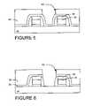
- FIGS. 1 through 7are cross sectional views for illustrating an etch method according to an aspect of the present invention.
- FIG. 8is a schematic view of a preferred plasma treatment tool according to an embodiment of the invention.
- FIG. 9is a schematic view of a preferred heating tool according to an embodiment of the invention.
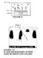
- FIG. 10is a x-SEM micrograph showing a void in oxide gap filling.
- FIG. 11is a x-SEM micrograph after a highly selective contact oxide etching that shows the reside oxide spacer within the contact hole.
- FIG. 12is a SEM micrograph showing the oxide residual spacer formed during the contact opening etch.
- Embodimentsshow a method for removing a residue oxide spacer from a contact opening sidewall.
- a contact openingis etched into a dielectric layer comprised of oxide. The etch process creates an undesired residual oxide spacer on the contact opening sidewall.
- a plasma treatment using nitrogen, fluorine and hydrogen containing gassese.g., NF 3 and N 2 +H 2
- nitrogen, fluorine and hydrogen containing gassese.g., NF 3 and N 2 +H 2
- the by-products layer and the undesired residual oxide spacerare preferably removed using one of the following: (1) heating, (2) DI rinse and (3) UV radiation. See FIG. 5 .
- Some embodimentsprovide a method of forming a contact hole.
- An aspect of the inventionis a method of fabrication a contact hole. Aspects remove an oxide residue and an oxide spacer beside a nitride spacer after an oxide etch. An embodiment of the process is described as follows.
- the gate structureis preferably comprised of a gate dielectric 20 , a gate electrode 24 and a nitride hard mask 26 .
- the nitride spacers 30are preferably comprised of nitride and preferably have a thickness of between 300 and 2000 ⁇ .
- nitride liner 36over the nitride spacers 30 and the gate structure 20 24 26 and the substrate 10 .
- the nitride liner 36preferably has a thickness between 50 and 1500 ⁇ .
- a dielectric layer 50preferably comprised of oxide over the nitride liner 36 .
- the dielectric layer 50is preferably formed by a HDP oxide or BPSG oxide process and has a thickness between 3000 and 10,000 ⁇ .
- the photoresist patternhas an opening over a contact area.
- the contact opening 60exposes the nitride liner on the gate structure sidewalls and on the substrate adjacent the gate structure.
- the residue spacer 70is on the sidewalls of the nitride spacer.
- the residual spaceris preferably mostly comprised of oxide (from the dielectric layer 50 ) and is preferably greater than 90% oxide and is preferably greater than 99% oxide.
- the residual spacerusually has a thickness of less than 150 ⁇ .
- the polymer layer 71is preferably over the residual spacer 70 , the nitride line 36 , the sidewalls of the dielectric layer 50 .
- the polymer layer 71is thought to be comprised of a CxHyFz.
- the etch process of the contact openingpreferably comprises: a RF bias power between 500 and 1000 W, a process pressure between 5 and 200 mTorr, a carbon fluoride containing gas (such as C x F y , C 4 F 8 or C 5 F 8 , C 4 F 6 , C 2 F 4 , etc.) with a flow between 3 and 50 sccm, a O 2 flow between 0 and 50 sccm, a CH 2 F 2 (or CH 3 F) flow between 0 and 50 sccm, an inert gas (such as Ar or He) flow between 0 and 1000 sccm.
- a RF bias powerbetween 500 and 1000 W
- a process pressurebetween 5 and 200 mTorr
- a carbon fluoride containing gassuch as C x F y , C 4 F 8 or C 5 F 8 , C 4 F 6 , C 2 F 4 , etc.
- This highly selectively oxide etching to nitride using a high polymerization gas like C 4 F 8 , C 5 F 8 , C 4 F 6is used to get high selectivity oxide to nitride.
- the polymer layer 71e.g., C x H y F z
- the polymer layer 71generated during oxide etching can give less nitride etching rate and higher oxide etching rate to lead to high selectivity oxide to nitride.
- the stripping processpreferably comprises: a microwave bias power between 100 and 1000 W, a process pressure between 5 and 5000 mTorr., a O 2 /N 2 ratio between 10:1 and 20:1.
- a plasma treatment toolAs shown in FIG. 4 , we place the substrate into a plasma treatment tool and perform plasma treatment preferably using a fluorine (F), nitrogen (N) and hydrogen (H) (elements) containing gasses.
- the plasma treatmentreacts with the residual spacer 70 and forms a by-products layer 72 on sidewalls of the contact opening (the nitride liner 36 , the dielectric layer 50 , residue spacer 70 ).
- the plasma treatment gasesare preferably NF 3 (nitrogen trifluoride) and nitrogen (N 2 ) & hydrogen (H 2 ).
- the by-products layer 72is preferably comprised of NxHyFz.
- the plasma treatmentpreferably comprises flowing NF 3 between 5 and 1000 sccm, flowing N2 between 5 and 5000 sccm, flowing H 2 between 5 and 2000 sccm, at a microwave power between 50 and 5000 W; the nitrogen and hydrogen feeds are a “Microwave (MW) down stream” plasma feed.
- the plasma treatmentmore preferably comprises flowing NF 3 between 10 and 500 sccm, flowing N 2 between 500 and 5000 sccm, flowing H 2 between 10 and 500 sccm, at a microwave power between 50 and 5000 W; the nitrogen and hydrogen feeds are preferably a “Microwave (MW) down stream” plasma feed.
- the plasma treatmentpreferably comprises flowing gas with a molar composition of NF 3 % between 1 and 75%, N 2 between 1 and 99% sccm, flowing H 2 between 1 and 75%, at a microwave power between 50 and 5000 W;
- the nitrogen and hydrogen feedsare a “Microwave (MW) down stream” plasma feed.
- the nitrogen and hydrogen feedspass thru the plasma applicator 110 before entering the chamber.
- the NH 3 flow inletis after the plasma applicator 110 and before the chamber.
- the NF 3 feedpreferably does not pass thru the plasma applicator.
- the plasma treatment toolpreferably selected from the group consisting of a Microwave tool, ICP tool, a MERIE tool, and a RIE tool.
- the waferis transferred from the photoresist stripper tool to a preferred plasma treatment tool with a downstream plasma chamber. See FIG. 8 .
- the plasma sourceis upstream of the chamber and not in the chamber.
- N 2 +H 2 gasto vacuum chamber through top gas inlet port.
- the N 2 +H 2flows thru the top inlet tube 122 to the plasma applicator device 110 that is connect to a microwave 112 .
- the microwaveexcites the N 2 and H 2 .
- the N 2 and H 2 plasmaflows thru the inlet tube 120 into the chamber 100 .
- the plasma treatmentpreferably comprises flowing gas with a molar composition of NF 3 % between 1 and 30%, N 2 between 70 and 95% sccm, flowing H 2 between 1 and 30%, at a microwave power between 50 and 5000 W.
- the NH 3 feedpreferably does not pass thru the plasma applicator.
- the nitrogen and hydrogen feedspass thru the plasma applicator 110 before entering the chamber.
- the NF 3 flow inletis after the plasma applicator 110 and before the chamber.
- N 2 and H 2 plasmacan react with the NF 3 to produce the F-contained activated radicals.
- the NF 3 gascan be activated to lead to radicals (such as NF 2 +, F ⁇ ) as FIG. 8 .
- the radicalscan react with H 2 to from by-products composed of for example NxHyFz.
- a by-products layer 72on the wafer which can be comprised of N x H y F z with x between 1 and 10; Y between 1 and 7; and z between 1 and 7.
- FIG. 9shows an example of a heating chamber 200 used to remove the residual oxide spacer and the by-products layer.
- FIG. 9shows a heater 220 heating a wafer 210 and the gases from the process.
- the waferis preferably heated to a temperature greater than 50° C. in preferably a N 2 gas (but can be air), a preferably atmospheric pressure.
- the residual oxide spacer and N x H y F z by-productspreferably are removed by the following reaction: SiO 2 +N x H y F z —heat and/or DI ⁇ SiH 4 +NH 3 +N 2 +H 2 O( g ) +O 2 + . . . others (A)
- the residual oxide spacer and N x H y F z by-products are removedare removed.
- the N x H y F z by-products layeris soluble in water.
- the Freacts to become HF.
- the HF in the watercan etch and remove the remaining residual oxide spacer.
- the N x H y F z by-products layercan also be removed by UV radiation.
- the reaction to remove the N x H y F z by-products layeris so similar to the above shown for heating.
- nitride linerpreferably using a nitride etch (selective to oxide) to expose the surface of the substrate in the contact opening 60 .
- the nitride etchpreferably comprises using CH 2 F 2 (or CH 3 F, CF 4 , NF 3 , SF 6 , . . . ) at a flow between 1 and 500 sccm, O2 (or N2) flow between 0 and 500 sccm, Ar (or He) flow between 0 and 1000 sccm, a RF power between 10 and 1000 W.
- the etchcan be performed in a MERIE (or DRM, ICP, TCP, DPS, Microwave,) plasma tool
- FIGS. 10 , 11 and 12there is shown a structure over which some embodiments are an improvement. It is to be understood in this regard that no portion of FIGS. 10 , 11 and 12 are admitted to be prior art as the present invention. Rather, this highly simplified diagram is an effort to provide an improved understanding of the problems that are overcome by some of the embodiments. The recognition of the problem was important.
- SACSelf-Aligned Contact
- FIG. 12is a X-SEM micrograph after highly selectively etching to nitride shows an oxide spacer beside a nitride spacer.
- Embodimentscan also remove oxide residue within contact hole due to void. But this process cannot enlarge void because this process is self limited after some amount of etching oxide and self-closed by by-product.
- Embodimentscan make contact area enlarged to lead to decrease contact resistance to get better quality of device characteristics. Embodiments can also make better yield of device to remove oxide residue within contact hole that can cause particles within contact hole during pre-cleaning of Ar sputter before deposition of metal layer.
Landscapes
- Engineering & Computer Science (AREA)
- General Physics & Mathematics (AREA)
- Physics & Mathematics (AREA)
- Condensed Matter Physics & Semiconductors (AREA)
- Manufacturing & Machinery (AREA)
- Computer Hardware Design (AREA)
- Microelectronics & Electronic Packaging (AREA)
- Power Engineering (AREA)
- Chemical & Material Sciences (AREA)
- General Chemical & Material Sciences (AREA)
- Chemical Kinetics & Catalysis (AREA)
- Inorganic Chemistry (AREA)
- Internal Circuitry In Semiconductor Integrated Circuit Devices (AREA)
Abstract
Description
SiO2+NxHyFz—heat and/or DI→SiH4+NH3+N2+H2O(g) +O2+ . . . others (A)
- 1) Highly selective contact oxide etching to form contact Metal 1 to Si-active without short between gate and W-plug of Metal 1 can be obtained by using high polymer gas like C2F4, C3F8, C4F8, C5F8, and C4F6.
- 2) PR strip is to remove photo mask.
- 3) Wet cleaning like SPM or APM is to remove polymer that is generated during highly selective oxide etching.
- 4) Nitride etching is to remove nitride that is used as etch barrier layer for highly selective contact oxide etching.
- 1) In the case of some void in gap-filling oxide like
FIG. 10 , some polymer fills this void and polymer within void prevents oxide etching so that oxide residue is formed within contact hole like SEMFIG. 11 . This oxide residue makes contact area decrease to lead to high contact resistance as well particle source.FIG. 10 is a X-SEM micrograph shows void in oxide gap-filling.FIG. 11 . is a X-SEM micrograph after highly selective contact oxide etching shows oxide residue within contact hole. - 2) Thin oxide spacer beside Si3N4 as SEM
FIG. 12 is formed by polymer blocking against oxide etching that decreases contact area and leads to high contact resistance. To remove this two kinds of oxide residue and oxide spacer, if wet cleaning like diluted HF and BOE is used, as contact hole sidewall etch rate is faster than oxide residue, void as well as contact hole size is enlarged. This makes metal gap-filling bad and cause higher electrical short between contact hole through enlarged void. Therefore, unique method to remove little amount of oxide, diluted wet etching like HF and BOE, cannot be used to remove oxide residue and thin oxide spacer.
- 1) In the case of some void in gap-filling oxide like
Claims (26)
Priority Applications (2)
| Application Number | Priority Date | Filing Date | Title |
|---|---|---|---|
| US10/778,293US7291550B2 (en) | 2004-02-13 | 2004-02-13 | Method to form a contact hole |
| SG200407758ASG114681A1 (en) | 2004-02-13 | 2004-12-17 | Method to form a contact hole |
Applications Claiming Priority (1)
| Application Number | Priority Date | Filing Date | Title |
|---|---|---|---|
| US10/778,293US7291550B2 (en) | 2004-02-13 | 2004-02-13 | Method to form a contact hole |
Publications (2)
| Publication Number | Publication Date |
|---|---|
| US20050181588A1 US20050181588A1 (en) | 2005-08-18 |
| US7291550B2true US7291550B2 (en) | 2007-11-06 |
Family
ID=34838150
Family Applications (1)
| Application Number | Title | Priority Date | Filing Date |
|---|---|---|---|
| US10/778,293Expired - Fee RelatedUS7291550B2 (en) | 2004-02-13 | 2004-02-13 | Method to form a contact hole |
Country Status (2)
| Country | Link |
|---|---|
| US (1) | US7291550B2 (en) |
| SG (1) | SG114681A1 (en) |
Cited By (7)
| Publication number | Priority date | Publication date | Assignee | Title |
|---|---|---|---|---|
| US20080188081A1 (en)* | 2007-02-05 | 2008-08-07 | Lam Research Corporation | Ultra-high aspect ratio dielectric etch |
| US20090087978A1 (en)* | 2007-10-01 | 2009-04-02 | Nanya Technology Corporation | Interconnect manufacturing process |
| US20110237080A1 (en)* | 2010-03-29 | 2011-09-29 | Tokyo Electron Limited | Method for integrating low-k dielectrics |
| US20130075823A1 (en)* | 2011-09-28 | 2013-03-28 | Globalfoundries Singapore Pte. Ltd. | Reliable contacts |
| US9761583B2 (en)* | 2015-06-09 | 2017-09-12 | Commissariat A L'energie Atomique Et Aux Energies Alternatives | Manufacturing of self aligned interconnection elements for 3D integrated circuits |
| US9831182B2 (en)* | 2015-09-24 | 2017-11-28 | International Business Machines Corporation | Multiple pre-clean processes for interconnect fabrication |
| TWI882002B (en)* | 2019-08-30 | 2025-05-01 | 美商應用材料股份有限公司 | Methods and apparatus for cleaning metal contacts |
Families Citing this family (167)
| Publication number | Priority date | Publication date | Assignee | Title |
|---|---|---|---|---|
| KR100645458B1 (en)* | 2003-10-02 | 2006-11-13 | 주식회사 하이닉스반도체 | Manufacturing method of semiconductor device which can prevent attack by wet cleaning |
| KR100549014B1 (en)* | 2004-07-21 | 2006-02-02 | 삼성전자주식회사 | Semiconductor Devices Having A Spacer Pattern And Methods Of Forming The Same |
| KR100615583B1 (en)* | 2004-08-11 | 2006-08-25 | 삼성전자주식회사 | Methods of Forming P-RAM with Phase Transition Film Pattern Constrained by Node Insulation Pattern |
| US7723229B2 (en)* | 2005-04-22 | 2010-05-25 | Macronix International Co., Ltd. | Process of forming a self-aligned contact in a semiconductor device |
| KR100677998B1 (en)* | 2005-09-30 | 2007-02-02 | 동부일렉트로닉스 주식회사 | Shallow Trench Isolation Method for Semiconductor Devices |
| US8399360B1 (en)* | 2005-11-17 | 2013-03-19 | Cypress Semiconductor Corporation | Process for post contact-etch clean |
| US8052799B2 (en)* | 2006-10-12 | 2011-11-08 | International Business Machines Corporation | By-product collecting processes for cleaning processes |
| US8551880B2 (en)* | 2007-11-01 | 2013-10-08 | Applied Materials, Inc. | Ammonia-based plasma treatment for metal fill in narrow features |
| US8614151B2 (en)* | 2008-01-04 | 2013-12-24 | Micron Technology, Inc. | Method of etching a high aspect ratio contact |
| US8211808B2 (en)* | 2009-08-31 | 2012-07-03 | Applied Materials, Inc. | Silicon-selective dry etch for carbon-containing films |
| US9324576B2 (en) | 2010-05-27 | 2016-04-26 | Applied Materials, Inc. | Selective etch for silicon films |
| US8741778B2 (en) | 2010-12-14 | 2014-06-03 | Applied Materials, Inc. | Uniform dry etch in two stages |
| US10283321B2 (en) | 2011-01-18 | 2019-05-07 | Applied Materials, Inc. | Semiconductor processing system and methods using capacitively coupled plasma |
| US8771539B2 (en) | 2011-02-22 | 2014-07-08 | Applied Materials, Inc. | Remotely-excited fluorine and water vapor etch |
| US8999856B2 (en) | 2011-03-14 | 2015-04-07 | Applied Materials, Inc. | Methods for etch of sin films |
| US9064815B2 (en) | 2011-03-14 | 2015-06-23 | Applied Materials, Inc. | Methods for etch of metal and metal-oxide films |
| US8771536B2 (en) | 2011-08-01 | 2014-07-08 | Applied Materials, Inc. | Dry-etch for silicon-and-carbon-containing films |
| US8679982B2 (en) | 2011-08-26 | 2014-03-25 | Applied Materials, Inc. | Selective suppression of dry-etch rate of materials containing both silicon and oxygen |
| US8679983B2 (en) | 2011-09-01 | 2014-03-25 | Applied Materials, Inc. | Selective suppression of dry-etch rate of materials containing both silicon and nitrogen |
| US8927390B2 (en) | 2011-09-26 | 2015-01-06 | Applied Materials, Inc. | Intrench profile |
| US8808563B2 (en) | 2011-10-07 | 2014-08-19 | Applied Materials, Inc. | Selective etch of silicon by way of metastable hydrogen termination |
| WO2013070436A1 (en) | 2011-11-08 | 2013-05-16 | Applied Materials, Inc. | Methods of reducing substrate dislocation during gapfill processing |
| US9267739B2 (en) | 2012-07-18 | 2016-02-23 | Applied Materials, Inc. | Pedestal with multi-zone temperature control and multiple purge capabilities |
| US9373517B2 (en) | 2012-08-02 | 2016-06-21 | Applied Materials, Inc. | Semiconductor processing with DC assisted RF power for improved control |
| US9034770B2 (en) | 2012-09-17 | 2015-05-19 | Applied Materials, Inc. | Differential silicon oxide etch |
| US9023734B2 (en) | 2012-09-18 | 2015-05-05 | Applied Materials, Inc. | Radical-component oxide etch |
| US9390937B2 (en) | 2012-09-20 | 2016-07-12 | Applied Materials, Inc. | Silicon-carbon-nitride selective etch |
| US9132436B2 (en) | 2012-09-21 | 2015-09-15 | Applied Materials, Inc. | Chemical control features in wafer process equipment |
| US8765574B2 (en) | 2012-11-09 | 2014-07-01 | Applied Materials, Inc. | Dry etch process |
| US8969212B2 (en) | 2012-11-20 | 2015-03-03 | Applied Materials, Inc. | Dry-etch selectivity |
| US9064816B2 (en) | 2012-11-30 | 2015-06-23 | Applied Materials, Inc. | Dry-etch for selective oxidation removal |
| US8980763B2 (en) | 2012-11-30 | 2015-03-17 | Applied Materials, Inc. | Dry-etch for selective tungsten removal |
| US9111877B2 (en) | 2012-12-18 | 2015-08-18 | Applied Materials, Inc. | Non-local plasma oxide etch |
| US8921234B2 (en) | 2012-12-21 | 2014-12-30 | Applied Materials, Inc. | Selective titanium nitride etching |
| US10256079B2 (en) | 2013-02-08 | 2019-04-09 | Applied Materials, Inc. | Semiconductor processing systems having multiple plasma configurations |
| US9362130B2 (en) | 2013-03-01 | 2016-06-07 | Applied Materials, Inc. | Enhanced etching processes using remote plasma sources |
| US9040422B2 (en) | 2013-03-05 | 2015-05-26 | Applied Materials, Inc. | Selective titanium nitride removal |
| US8801952B1 (en) | 2013-03-07 | 2014-08-12 | Applied Materials, Inc. | Conformal oxide dry etch |
| US10170282B2 (en) | 2013-03-08 | 2019-01-01 | Applied Materials, Inc. | Insulated semiconductor faceplate designs |
| US20140271097A1 (en) | 2013-03-15 | 2014-09-18 | Applied Materials, Inc. | Processing systems and methods for halide scavenging |
| US8895449B1 (en) | 2013-05-16 | 2014-11-25 | Applied Materials, Inc. | Delicate dry clean |
| US9114438B2 (en) | 2013-05-21 | 2015-08-25 | Applied Materials, Inc. | Copper residue chamber clean |
| US9493879B2 (en) | 2013-07-12 | 2016-11-15 | Applied Materials, Inc. | Selective sputtering for pattern transfer |
| US20150050812A1 (en)* | 2013-08-13 | 2015-02-19 | Globalfoundries Inc. | Wafer-less auto clean of processing chamber |
| US20150064921A1 (en)* | 2013-08-30 | 2015-03-05 | Applied Materials, Inc. | Low temperature plasma anneal process for sublimative etch processes |
| US9773648B2 (en) | 2013-08-30 | 2017-09-26 | Applied Materials, Inc. | Dual discharge modes operation for remote plasma |
| US8956980B1 (en) | 2013-09-16 | 2015-02-17 | Applied Materials, Inc. | Selective etch of silicon nitride |
| US8951429B1 (en) | 2013-10-29 | 2015-02-10 | Applied Materials, Inc. | Tungsten oxide processing |
| US9236265B2 (en) | 2013-11-04 | 2016-01-12 | Applied Materials, Inc. | Silicon germanium processing |
| US9576809B2 (en) | 2013-11-04 | 2017-02-21 | Applied Materials, Inc. | Etch suppression with germanium |
| US9520303B2 (en) | 2013-11-12 | 2016-12-13 | Applied Materials, Inc. | Aluminum selective etch |
| US9245762B2 (en) | 2013-12-02 | 2016-01-26 | Applied Materials, Inc. | Procedure for etch rate consistency |
| US9117855B2 (en) | 2013-12-04 | 2015-08-25 | Applied Materials, Inc. | Polarity control for remote plasma |
| US9263278B2 (en) | 2013-12-17 | 2016-02-16 | Applied Materials, Inc. | Dopant etch selectivity control |
| US9287095B2 (en) | 2013-12-17 | 2016-03-15 | Applied Materials, Inc. | Semiconductor system assemblies and methods of operation |
| US9190293B2 (en) | 2013-12-18 | 2015-11-17 | Applied Materials, Inc. | Even tungsten etch for high aspect ratio trenches |
| US9287134B2 (en) | 2014-01-17 | 2016-03-15 | Applied Materials, Inc. | Titanium oxide etch |
| US9396989B2 (en) | 2014-01-27 | 2016-07-19 | Applied Materials, Inc. | Air gaps between copper lines |
| US9293568B2 (en) | 2014-01-27 | 2016-03-22 | Applied Materials, Inc. | Method of fin patterning |
| US9385028B2 (en) | 2014-02-03 | 2016-07-05 | Applied Materials, Inc. | Air gap process |
| US9499898B2 (en) | 2014-03-03 | 2016-11-22 | Applied Materials, Inc. | Layered thin film heater and method of fabrication |
| US9299575B2 (en) | 2014-03-17 | 2016-03-29 | Applied Materials, Inc. | Gas-phase tungsten etch |
| US9299537B2 (en) | 2014-03-20 | 2016-03-29 | Applied Materials, Inc. | Radial waveguide systems and methods for post-match control of microwaves |
| US9299538B2 (en) | 2014-03-20 | 2016-03-29 | Applied Materials, Inc. | Radial waveguide systems and methods for post-match control of microwaves |
| US9136273B1 (en) | 2014-03-21 | 2015-09-15 | Applied Materials, Inc. | Flash gate air gap |
| US9903020B2 (en) | 2014-03-31 | 2018-02-27 | Applied Materials, Inc. | Generation of compact alumina passivation layers on aluminum plasma equipment components |
| US9269590B2 (en) | 2014-04-07 | 2016-02-23 | Applied Materials, Inc. | Spacer formation |
| US9309598B2 (en) | 2014-05-28 | 2016-04-12 | Applied Materials, Inc. | Oxide and metal removal |
| US9847289B2 (en) | 2014-05-30 | 2017-12-19 | Applied Materials, Inc. | Protective via cap for improved interconnect performance |
| US9378969B2 (en) | 2014-06-19 | 2016-06-28 | Applied Materials, Inc. | Low temperature gas-phase carbon removal |
| US9406523B2 (en) | 2014-06-19 | 2016-08-02 | Applied Materials, Inc. | Highly selective doped oxide removal method |
| JP6235981B2 (en)* | 2014-07-01 | 2017-11-22 | 東京エレクトロン株式会社 | Method for processing an object |
| US9425058B2 (en) | 2014-07-24 | 2016-08-23 | Applied Materials, Inc. | Simplified litho-etch-litho-etch process |
| US9159606B1 (en) | 2014-07-31 | 2015-10-13 | Applied Materials, Inc. | Metal air gap |
| US9378978B2 (en)* | 2014-07-31 | 2016-06-28 | Applied Materials, Inc. | Integrated oxide recess and floating gate fin trimming |
| US9496167B2 (en) | 2014-07-31 | 2016-11-15 | Applied Materials, Inc. | Integrated bit-line airgap formation and gate stack post clean |
| US9165786B1 (en) | 2014-08-05 | 2015-10-20 | Applied Materials, Inc. | Integrated oxide and nitride recess for better channel contact in 3D architectures |
| US9659753B2 (en) | 2014-08-07 | 2017-05-23 | Applied Materials, Inc. | Grooved insulator to reduce leakage current |
| EP2988322B1 (en)* | 2014-08-18 | 2020-06-24 | IMEC vzw | Method for selective oxide removal |
| US9553102B2 (en) | 2014-08-19 | 2017-01-24 | Applied Materials, Inc. | Tungsten separation |
| US9355856B2 (en) | 2014-09-12 | 2016-05-31 | Applied Materials, Inc. | V trench dry etch |
| US9368364B2 (en) | 2014-09-24 | 2016-06-14 | Applied Materials, Inc. | Silicon etch process with tunable selectivity to SiO2 and other materials |
| US9355862B2 (en) | 2014-09-24 | 2016-05-31 | Applied Materials, Inc. | Fluorine-based hardmask removal |
| US9613822B2 (en) | 2014-09-25 | 2017-04-04 | Applied Materials, Inc. | Oxide etch selectivity enhancement |
| US9966240B2 (en) | 2014-10-14 | 2018-05-08 | Applied Materials, Inc. | Systems and methods for internal surface conditioning assessment in plasma processing equipment |
| US9355922B2 (en) | 2014-10-14 | 2016-05-31 | Applied Materials, Inc. | Systems and methods for internal surface conditioning in plasma processing equipment |
| US11637002B2 (en) | 2014-11-26 | 2023-04-25 | Applied Materials, Inc. | Methods and systems to enhance process uniformity |
| US9299583B1 (en) | 2014-12-05 | 2016-03-29 | Applied Materials, Inc. | Aluminum oxide selective etch |
| US10224210B2 (en) | 2014-12-09 | 2019-03-05 | Applied Materials, Inc. | Plasma processing system with direct outlet toroidal plasma source |
| US10573496B2 (en) | 2014-12-09 | 2020-02-25 | Applied Materials, Inc. | Direct outlet toroidal plasma source |
| US9502258B2 (en) | 2014-12-23 | 2016-11-22 | Applied Materials, Inc. | Anisotropic gap etch |
| US9343272B1 (en) | 2015-01-08 | 2016-05-17 | Applied Materials, Inc. | Self-aligned process |
| US11257693B2 (en) | 2015-01-09 | 2022-02-22 | Applied Materials, Inc. | Methods and systems to improve pedestal temperature control |
| US9373522B1 (en) | 2015-01-22 | 2016-06-21 | Applied Mateials, Inc. | Titanium nitride removal |
| US9449846B2 (en) | 2015-01-28 | 2016-09-20 | Applied Materials, Inc. | Vertical gate separation |
| US20160225652A1 (en) | 2015-02-03 | 2016-08-04 | Applied Materials, Inc. | Low temperature chuck for plasma processing systems |
| US9728437B2 (en) | 2015-02-03 | 2017-08-08 | Applied Materials, Inc. | High temperature chuck for plasma processing systems |
| US9881805B2 (en) | 2015-03-02 | 2018-01-30 | Applied Materials, Inc. | Silicon selective removal |
| US9741593B2 (en) | 2015-08-06 | 2017-08-22 | Applied Materials, Inc. | Thermal management systems and methods for wafer processing systems |
| US9691645B2 (en) | 2015-08-06 | 2017-06-27 | Applied Materials, Inc. | Bolted wafer chuck thermal management systems and methods for wafer processing systems |
| US9349605B1 (en) | 2015-08-07 | 2016-05-24 | Applied Materials, Inc. | Oxide etch selectivity systems and methods |
| US10504700B2 (en) | 2015-08-27 | 2019-12-10 | Applied Materials, Inc. | Plasma etching systems and methods with secondary plasma injection |
| US10522371B2 (en) | 2016-05-19 | 2019-12-31 | Applied Materials, Inc. | Systems and methods for improved semiconductor etching and component protection |
| US10504754B2 (en) | 2016-05-19 | 2019-12-10 | Applied Materials, Inc. | Systems and methods for improved semiconductor etching and component protection |
| US20170345673A1 (en)* | 2016-05-29 | 2017-11-30 | Tokyo Electron Limited | Method of selective silicon oxide etching |
| US9865484B1 (en) | 2016-06-29 | 2018-01-09 | Applied Materials, Inc. | Selective etch using material modification and RF pulsing |
| US10062575B2 (en) | 2016-09-09 | 2018-08-28 | Applied Materials, Inc. | Poly directional etch by oxidation |
| US10629473B2 (en) | 2016-09-09 | 2020-04-21 | Applied Materials, Inc. | Footing removal for nitride spacer |
| US10546729B2 (en) | 2016-10-04 | 2020-01-28 | Applied Materials, Inc. | Dual-channel showerhead with improved profile |
| US9721789B1 (en) | 2016-10-04 | 2017-08-01 | Applied Materials, Inc. | Saving ion-damaged spacers |
| US10062585B2 (en) | 2016-10-04 | 2018-08-28 | Applied Materials, Inc. | Oxygen compatible plasma source |
| US9934942B1 (en) | 2016-10-04 | 2018-04-03 | Applied Materials, Inc. | Chamber with flow-through source |
| US10062579B2 (en) | 2016-10-07 | 2018-08-28 | Applied Materials, Inc. | Selective SiN lateral recess |
| US9947549B1 (en) | 2016-10-10 | 2018-04-17 | Applied Materials, Inc. | Cobalt-containing material removal |
| US9768034B1 (en) | 2016-11-11 | 2017-09-19 | Applied Materials, Inc. | Removal methods for high aspect ratio structures |
| US10163696B2 (en) | 2016-11-11 | 2018-12-25 | Applied Materials, Inc. | Selective cobalt removal for bottom up gapfill |
| US10242908B2 (en) | 2016-11-14 | 2019-03-26 | Applied Materials, Inc. | Airgap formation with damage-free copper |
| US10026621B2 (en) | 2016-11-14 | 2018-07-17 | Applied Materials, Inc. | SiN spacer profile patterning |
| US10566206B2 (en) | 2016-12-27 | 2020-02-18 | Applied Materials, Inc. | Systems and methods for anisotropic material breakthrough |
| US10403507B2 (en) | 2017-02-03 | 2019-09-03 | Applied Materials, Inc. | Shaped etch profile with oxidation |
| US10431429B2 (en) | 2017-02-03 | 2019-10-01 | Applied Materials, Inc. | Systems and methods for radial and azimuthal control of plasma uniformity |
| US10043684B1 (en) | 2017-02-06 | 2018-08-07 | Applied Materials, Inc. | Self-limiting atomic thermal etching systems and methods |
| US10319739B2 (en) | 2017-02-08 | 2019-06-11 | Applied Materials, Inc. | Accommodating imperfectly aligned memory holes |
| US10943834B2 (en) | 2017-03-13 | 2021-03-09 | Applied Materials, Inc. | Replacement contact process |
| US10319649B2 (en) | 2017-04-11 | 2019-06-11 | Applied Materials, Inc. | Optical emission spectroscopy (OES) for remote plasma monitoring |
| JP7176860B6 (en) | 2017-05-17 | 2022-12-16 | アプライド マテリアルズ インコーポレイテッド | Semiconductor processing chamber to improve precursor flow |
| US11276559B2 (en) | 2017-05-17 | 2022-03-15 | Applied Materials, Inc. | Semiconductor processing chamber for multiple precursor flow |
| US11276590B2 (en) | 2017-05-17 | 2022-03-15 | Applied Materials, Inc. | Multi-zone semiconductor substrate supports |
| US10497579B2 (en) | 2017-05-31 | 2019-12-03 | Applied Materials, Inc. | Water-free etching methods |
| US10049891B1 (en) | 2017-05-31 | 2018-08-14 | Applied Materials, Inc. | Selective in situ cobalt residue removal |
| US10920320B2 (en) | 2017-06-16 | 2021-02-16 | Applied Materials, Inc. | Plasma health determination in semiconductor substrate processing reactors |
| US10541246B2 (en) | 2017-06-26 | 2020-01-21 | Applied Materials, Inc. | 3D flash memory cells which discourage cross-cell electrical tunneling |
| US10727080B2 (en) | 2017-07-07 | 2020-07-28 | Applied Materials, Inc. | Tantalum-containing material removal |
| US10541184B2 (en) | 2017-07-11 | 2020-01-21 | Applied Materials, Inc. | Optical emission spectroscopic techniques for monitoring etching |
| US10354889B2 (en) | 2017-07-17 | 2019-07-16 | Applied Materials, Inc. | Non-halogen etching of silicon-containing materials |
| US10170336B1 (en) | 2017-08-04 | 2019-01-01 | Applied Materials, Inc. | Methods for anisotropic control of selective silicon removal |
| US10043674B1 (en) | 2017-08-04 | 2018-08-07 | Applied Materials, Inc. | Germanium etching systems and methods |
| US10297458B2 (en) | 2017-08-07 | 2019-05-21 | Applied Materials, Inc. | Process window widening using coated parts in plasma etch processes |
| US10283324B1 (en) | 2017-10-24 | 2019-05-07 | Applied Materials, Inc. | Oxygen treatment for nitride etching |
| US10128086B1 (en) | 2017-10-24 | 2018-11-13 | Applied Materials, Inc. | Silicon pretreatment for nitride removal |
| US10256112B1 (en) | 2017-12-08 | 2019-04-09 | Applied Materials, Inc. | Selective tungsten removal |
| US10903054B2 (en) | 2017-12-19 | 2021-01-26 | Applied Materials, Inc. | Multi-zone gas distribution systems and methods |
| US11328909B2 (en) | 2017-12-22 | 2022-05-10 | Applied Materials, Inc. | Chamber conditioning and removal processes |
| US10854426B2 (en) | 2018-01-08 | 2020-12-01 | Applied Materials, Inc. | Metal recess for semiconductor structures |
| US10964512B2 (en) | 2018-02-15 | 2021-03-30 | Applied Materials, Inc. | Semiconductor processing chamber multistage mixing apparatus and methods |
| US10679870B2 (en) | 2018-02-15 | 2020-06-09 | Applied Materials, Inc. | Semiconductor processing chamber multistage mixing apparatus |
| TWI766433B (en) | 2018-02-28 | 2022-06-01 | 美商應用材料股份有限公司 | Systems and methods to form airgaps |
| US10593560B2 (en) | 2018-03-01 | 2020-03-17 | Applied Materials, Inc. | Magnetic induction plasma source for semiconductor processes and equipment |
| US10319600B1 (en) | 2018-03-12 | 2019-06-11 | Applied Materials, Inc. | Thermal silicon etch |
| US10497573B2 (en) | 2018-03-13 | 2019-12-03 | Applied Materials, Inc. | Selective atomic layer etching of semiconductor materials |
| US10573527B2 (en) | 2018-04-06 | 2020-02-25 | Applied Materials, Inc. | Gas-phase selective etching systems and methods |
| US10490406B2 (en) | 2018-04-10 | 2019-11-26 | Appled Materials, Inc. | Systems and methods for material breakthrough |
| US10699879B2 (en) | 2018-04-17 | 2020-06-30 | Applied Materials, Inc. | Two piece electrode assembly with gap for plasma control |
| US10886137B2 (en) | 2018-04-30 | 2021-01-05 | Applied Materials, Inc. | Selective nitride removal |
| US10755941B2 (en) | 2018-07-06 | 2020-08-25 | Applied Materials, Inc. | Self-limiting selective etching systems and methods |
| US10872778B2 (en) | 2018-07-06 | 2020-12-22 | Applied Materials, Inc. | Systems and methods utilizing solid-phase etchants |
| US10672642B2 (en) | 2018-07-24 | 2020-06-02 | Applied Materials, Inc. | Systems and methods for pedestal configuration |
| US11049755B2 (en) | 2018-09-14 | 2021-06-29 | Applied Materials, Inc. | Semiconductor substrate supports with embedded RF shield |
| US10892198B2 (en) | 2018-09-14 | 2021-01-12 | Applied Materials, Inc. | Systems and methods for improved performance in semiconductor processing |
| US11062887B2 (en) | 2018-09-17 | 2021-07-13 | Applied Materials, Inc. | High temperature RF heater pedestals |
| US11417534B2 (en) | 2018-09-21 | 2022-08-16 | Applied Materials, Inc. | Selective material removal |
| US11682560B2 (en) | 2018-10-11 | 2023-06-20 | Applied Materials, Inc. | Systems and methods for hafnium-containing film removal |
| US11121002B2 (en) | 2018-10-24 | 2021-09-14 | Applied Materials, Inc. | Systems and methods for etching metals and metal derivatives |
| US11437242B2 (en) | 2018-11-27 | 2022-09-06 | Applied Materials, Inc. | Selective removal of silicon-containing materials |
| US11721527B2 (en) | 2019-01-07 | 2023-08-08 | Applied Materials, Inc. | Processing chamber mixing systems |
| US10920319B2 (en) | 2019-01-11 | 2021-02-16 | Applied Materials, Inc. | Ceramic showerheads with conductive electrodes |
| US12057299B2 (en)* | 2021-09-27 | 2024-08-06 | Applied Materials, Inc. | Methods for selective removal of contact oxides |
Citations (4)
| Publication number | Priority date | Publication date | Assignee | Title |
|---|---|---|---|---|
| US5423945A (en) | 1992-09-08 | 1995-06-13 | Applied Materials, Inc. | Selectivity for etching an oxide over a nitride |
| US5505816A (en) | 1993-12-16 | 1996-04-09 | International Business Machines Corporation | Etching of silicon dioxide selectively to silicon nitride and polysilicon |
| US6536449B1 (en) | 1997-11-17 | 2003-03-25 | Mattson Technology Inc. | Downstream surface cleaning process |
| US6583065B1 (en) | 1999-08-03 | 2003-06-24 | Applied Materials Inc. | Sidewall polymer forming gas additives for etching processes |
- 2004
- 2004-02-13USUS10/778,293patent/US7291550B2/ennot_activeExpired - Fee Related
- 2004-12-17SGSG200407758Apatent/SG114681A1/enunknown
Patent Citations (4)
| Publication number | Priority date | Publication date | Assignee | Title |
|---|---|---|---|---|
| US5423945A (en) | 1992-09-08 | 1995-06-13 | Applied Materials, Inc. | Selectivity for etching an oxide over a nitride |
| US5505816A (en) | 1993-12-16 | 1996-04-09 | International Business Machines Corporation | Etching of silicon dioxide selectively to silicon nitride and polysilicon |
| US6536449B1 (en) | 1997-11-17 | 2003-03-25 | Mattson Technology Inc. | Downstream surface cleaning process |
| US6583065B1 (en) | 1999-08-03 | 2003-06-24 | Applied Materials Inc. | Sidewall polymer forming gas additives for etching processes |
Non-Patent Citations (1)
| Title |
|---|
| Hu et al., "Resist stripping for multilevel interconnect integration with Low K dielectric material", AVS first inter conference on Microelectronics and interfaces, Feb. 2000. |
Cited By (15)
| Publication number | Priority date | Publication date | Assignee | Title |
|---|---|---|---|---|
| US8906194B2 (en) | 2007-02-05 | 2014-12-09 | Lam Research Corporation | Ultra-high aspect ratio dielectric etch |
| US7682986B2 (en)* | 2007-02-05 | 2010-03-23 | Lam Research Corporation | Ultra-high aspect ratio dielectric etch |
| US20100132889A1 (en)* | 2007-02-05 | 2010-06-03 | Lam Research Corporation | Ultra-high aspect ratio dielectric etch |
| US20080188081A1 (en)* | 2007-02-05 | 2008-08-07 | Lam Research Corporation | Ultra-high aspect ratio dielectric etch |
| US20090087978A1 (en)* | 2007-10-01 | 2009-04-02 | Nanya Technology Corporation | Interconnect manufacturing process |
| US20110237080A1 (en)* | 2010-03-29 | 2011-09-29 | Tokyo Electron Limited | Method for integrating low-k dielectrics |
| US9017933B2 (en)* | 2010-03-29 | 2015-04-28 | Tokyo Electron Limited | Method for integrating low-k dielectrics |
| US8519482B2 (en)* | 2011-09-28 | 2013-08-27 | Globalfoundries Singapore Pte. Ltd. | Reliable contacts |
| US20130334616A1 (en)* | 2011-09-28 | 2013-12-19 | GLOBALFOUNDRIER Singapore Pte. Ltd. | Reliable contacts |
| US8916939B2 (en)* | 2011-09-28 | 2014-12-23 | Globalfoundries Singapore Pte. Ltd. | Reliable contacts |
| US20130075823A1 (en)* | 2011-09-28 | 2013-03-28 | Globalfoundries Singapore Pte. Ltd. | Reliable contacts |
| US9761583B2 (en)* | 2015-06-09 | 2017-09-12 | Commissariat A L'energie Atomique Et Aux Energies Alternatives | Manufacturing of self aligned interconnection elements for 3D integrated circuits |
| US9831182B2 (en)* | 2015-09-24 | 2017-11-28 | International Business Machines Corporation | Multiple pre-clean processes for interconnect fabrication |
| US9887160B2 (en)* | 2015-09-24 | 2018-02-06 | International Business Machines Corporation | Multiple pre-clean processes for interconnect fabrication |
| TWI882002B (en)* | 2019-08-30 | 2025-05-01 | 美商應用材料股份有限公司 | Methods and apparatus for cleaning metal contacts |
Also Published As
| Publication number | Publication date |
|---|---|
| US20050181588A1 (en) | 2005-08-18 |
| SG114681A1 (en) | 2005-09-28 |
Similar Documents
| Publication | Publication Date | Title |
|---|---|---|
| US7291550B2 (en) | Method to form a contact hole | |
| JP5122106B2 (en) | Carbon-containing film etching method and semiconductor device manufacturing method using the same | |
| KR100679375B1 (en) | Masking method | |
| JP3027951B2 (en) | Method for manufacturing semiconductor device | |
| JP3152428B2 (en) | An improved method for forming local interconnects using selective anisotropy | |
| US6184119B1 (en) | Methods for reducing semiconductor contact resistance | |
| JP2004519102A (en) | Method of etching tungsten or tungsten nitride electrode gate in semiconductor structure | |
| US7273566B2 (en) | Gas compositions | |
| JP2006190947A (en) | Recess gate and method of manufacturing semiconductor device having the same | |
| KR20030027453A (en) | Method of dry cleaning and photoresist strip after via contact etching | |
| US7022618B2 (en) | Method of forming a conductive contact | |
| CN101231968B (en) | Damascene interconnect structure and dual damascene process | |
| KR100502673B1 (en) | METHOD FOR FORMING Ti LAYER AND BARRIER METAL LAYER OF SEMICONDUCTOR DEVICE | |
| US6803307B1 (en) | Method of avoiding enlargement of top critical dimension in contact holes using spacers | |
| US20030227092A1 (en) | Method of rounding a corner of a contact | |
| US6900104B1 (en) | Method of forming offset spacer manufacturing for critical dimension precision | |
| KR100680944B1 (en) | Manufacturing method of semiconductor device | |
| JP2005327873A (en) | Semiconductor device and manufacturing method thereof | |
| JP3371179B2 (en) | Wiring formation method | |
| JP2005136097A (en) | Manufacturing method of semiconductor device | |
| US20240249936A1 (en) | Methods for reducing micro and macro scalloping on semiconductor devices | |
| KR20050000970A (en) | Method of manufacturing semiconductor device | |
| JP2001057382A (en) | Method for manufacturing semiconductor device | |
| JPH11204500A (en) | Manufacture of semiconductor device | |
| KR100548564B1 (en) | Bit line formation method |
Legal Events
| Date | Code | Title | Description |
|---|---|---|---|
| AS | Assignment | Owner name:CHARTERED SEMICONDUCTOR MANUFACTURING LTD, SINGAPO Free format text:ASSIGNMENT OF ASSIGNORS INTEREST;ASSIGNOR:KIM, JEONG-HO;REEL/FRAME:014992/0449 Effective date:20040210 | |
| AS | Assignment | Owner name:CHARTERED SEMICONDUCTOR MANUFACTURING LTD., SINGAP Free format text:ASSIGNMENT OF ASSIGNORS INTEREST;ASSIGNOR:KIM, JEONG-HO;REEL/FRAME:017169/0244 Effective date:20051122 | |
| STCF | Information on status: patent grant | Free format text:PATENTED CASE | |
| FPAY | Fee payment | Year of fee payment:4 | |
| FPAY | Fee payment | Year of fee payment:8 | |
| AS | Assignment | Owner name:GLOBALFOUNDRIES SINGAPORE PTE. LTD., SINGAPORE Free format text:CHANGE OF NAME;ASSIGNOR:CHARTERED SEMICONDUCTOR MANUFACTURING PTE. LTD.;REEL/FRAME:047614/0081 Effective date:20160107 | |
| FEPP | Fee payment procedure | Free format text:MAINTENANCE FEE REMINDER MAILED (ORIGINAL EVENT CODE: REM.); ENTITY STATUS OF PATENT OWNER: LARGE ENTITY | |
| AS | Assignment | Owner name:ALSEPHINA INNOVATIONS INC., CANADA Free format text:ASSIGNMENT OF ASSIGNORS INTEREST;ASSIGNOR:GLOBALFOUNDRIES SINGAPORE PTE. LTD.;REEL/FRAME:049669/0775 Effective date:20181126 | |
| LAPS | Lapse for failure to pay maintenance fees | Free format text:PATENT EXPIRED FOR FAILURE TO PAY MAINTENANCE FEES (ORIGINAL EVENT CODE: EXP.); ENTITY STATUS OF PATENT OWNER: LARGE ENTITY | |
| STCH | Information on status: patent discontinuation | Free format text:PATENT EXPIRED DUE TO NONPAYMENT OF MAINTENANCE FEES UNDER 37 CFR 1.362 | |
| FP | Expired due to failure to pay maintenance fee | Effective date:20191106 | |
| AS | Assignment | Owner name:TAIWAN SEMICONDUCTOR MANUFACTURING COMPANY, LTD., TAIWAN Free format text:ASSIGNMENT OF ASSIGNORS INTEREST;ASSIGNOR:ALSEPHINA INNOVATIONS, INC.;REEL/FRAME:053351/0839 Effective date:20200211 |