US7291529B2 - Methods of processing semiconductor wafer backsides having light emitting devices (LEDs) thereon - Google Patents
Methods of processing semiconductor wafer backsides having light emitting devices (LEDs) thereonDownload PDFInfo
- Publication number
- US7291529B2 US7291529B2US10/987,135US98713504AUS7291529B2US 7291529 B2US7291529 B2US 7291529B2US 98713504 AUS98713504 AUS 98713504AUS 7291529 B2US7291529 B2US 7291529B2
- Authority
- US
- United States
- Prior art keywords
- wafer
- thickness
- leds
- backside
- cutting
- Prior art date
- Legal status (The legal status is an assumption and is not a legal conclusion. Google has not performed a legal analysis and makes no representation as to the accuracy of the status listed.)
- Active, expires
Links
Images


Classifications
- H—ELECTRICITY
- H10—SEMICONDUCTOR DEVICES; ELECTRIC SOLID-STATE DEVICES NOT OTHERWISE PROVIDED FOR
- H10H—INORGANIC LIGHT-EMITTING SEMICONDUCTOR DEVICES HAVING POTENTIAL BARRIERS
- H10H20/00—Individual inorganic light-emitting semiconductor devices having potential barriers, e.g. light-emitting diodes [LED]
- H10H20/01—Manufacture or treatment
- H—ELECTRICITY
- H10—SEMICONDUCTOR DEVICES; ELECTRIC SOLID-STATE DEVICES NOT OTHERWISE PROVIDED FOR
- H10H—INORGANIC LIGHT-EMITTING SEMICONDUCTOR DEVICES HAVING POTENTIAL BARRIERS
- H10H20/00—Individual inorganic light-emitting semiconductor devices having potential barriers, e.g. light-emitting diodes [LED]
- H10H20/80—Constructional details
- H10H20/81—Bodies
- H10H20/819—Bodies characterised by their shape, e.g. curved or truncated substrates
- H—ELECTRICITY
- H01—ELECTRIC ELEMENTS
- H01L—SEMICONDUCTOR DEVICES NOT COVERED BY CLASS H10
- H01L21/00—Processes or apparatus adapted for the manufacture or treatment of semiconductor or solid state devices or of parts thereof
- H01L21/70—Manufacture or treatment of devices consisting of a plurality of solid state components formed in or on a common substrate or of parts thereof; Manufacture of integrated circuit devices or of parts thereof
- H01L21/77—Manufacture or treatment of devices consisting of a plurality of solid state components or integrated circuits formed in, or on, a common substrate
- H01L21/78—Manufacture or treatment of devices consisting of a plurality of solid state components or integrated circuits formed in, or on, a common substrate with subsequent division of the substrate into plural individual devices
Definitions
- This inventionrelates to microelectronic devices, and more particularly, to the fabrication of light emitting devices (LEDs) and LEDs so formed.
- LEDslight emitting devices
- SiC-based light emitting devicescan affect the forward voltage needed to operate the devices at a given current level.
- SiC-based light emitting diode C450-CB230-E1000 available from Cree, Inc.has a substrate thickness of about 250 ⁇ m (+/ ⁇ 25 ⁇ m) and has an associated forward operating voltage of about 3.5 volts at about 20 mA forward operating current.
- reducing the thickness of the SiC substrate of an LEDmay reduce the forward voltage, which may yield reduced power consumption in such diodes.
- ohmic contactson SiC at low/room temperature by, for example, implanting ions into a backside of a SiC wafer.
- the doped regionmay be removed during the thinning, which may make the implant superfluous.
- metals deposited form ohmic contactsmay not have ohmic properties when deposited on the substrate as the implant may be performed in a later step. Ion implantation for the formation of ohmic contacts is discussed, for example, in U.S. patent application Ser. No. 09/787,189, and in U.S. Patent Publication No. US 2002/0179910, the disclosures of which are incorporated herein by reference in their entireties as if set forth fully herein.
- metal ohmic contactsby depositing a metal, such as nickel, and annealing the metal at a high temperature (such as temperatures greater than 900 C). High temperature annealing may damage epitaxial layers of gallium nitride based materials included on the SiC substrate.
- FIGS. 1-7are cross-sectional illustrations that illustrate methods of processing semiconductor wafers according to some embodiments of the invention.
- FIGS. 8 and 9are a cross-sectional view and an isometric view of a light emitting device having a laser patterned wafer according to various embodiments of the invention.
- FIGS. 10 through 13are cross-sectional views of laser patterned wafers according to alternative embodiments of the invention.
- FIGS. 14 through 16are cross-sectional view illustrating operations according to laser patterning techniques according to alternative embodiments of the invention.
- Embodiments according to the inventioncan provide methods of processing semiconductor wafer backsides having light emitting devices (LEDs) thereon and LEDs so formed.
- a method of processing a semiconductor wafercan include forming a plurality of Light Emitting Devices (LED) on a semiconductor wafer having a first thickness.
- the plurality of LEDs on the waferare coupled to a carrier.
- the first thickness of the waferis reduced to a second thickness that is less than the first thickness by processing the backside of the wafer.
- the carrieris separated from the plurality of LEDs on the wafer and the wafer is cut to separate the plurality of LEDs from one another.
- the first thicknessis from about 250 ⁇ m to about 400 ⁇ m.
- reducing the first thickness of the waferincludes grinding, lapping, and/or etching the backside of the wafer to reduce the first thickness of the wafer to the second thickness of less than about 150 ⁇ m.
- reducing the first thickness of the waferincludes grinding, lapping, and/or etching the backside of the wafer to reduce the first thickness of the wafer to the second thickness of less than about 120 ⁇ m.
- grinding the backside of the waferincludes grinding the backside of the wafer using an in-feed grinder or a creep feed grinder.
- cutting the waferincludes cutting the wafer using a saw blade to form straight edges on the separated plurality of LEDs.
- cutting the waferincludes cutting score lines on the wafer to form beveled grooves between the plurality of LEDs on the wafer and separating the plurality of LEDs on the wafer from one another along the score lines.
- cutting the waferincludes cutting the wafer with a saw blade to depth beneath a surface of the wafer of less than about a length of a beveled tip of the saw blade. In some embodiments according to the invention, the depth is less than about 120 ⁇ m.
- reducing the first thickness of the wafer to a second thicknessis followed by processing the backside surface of the wafer opposite the plurality of LEDs to improve light extraction.
- a plurality of respective contactsare formed on the backside surface opposite where respective bonding pads are to be formed on the plurality of LEDs.
- forming a plurality of respective contactsincludes forming a plurality of ohmic contacts using laser annealing.
- processingincludes etching the backside surface. In some embodiments according to the invention, processing includes laser patterning the backside surface.
- separating the carrier from the plurality of LEDs on the waferincludes heating, dissolving, or melting an adhesive layer sufficient to cause separation of the plurality of LEDs from the carrier.
- the waferis a Silicon Carbide or sapphire wafer.
- a light emitting device (LED) on a Silicon Carbide (SiC) substratehas a first thickness of less than about 150 ⁇ m.
- a forward voltage associated with the SiC substrateis about 3.4 volts.
- the SiC substrateis 4H—SiC or 6H—SiC.
- first, second, etc.may be used herein to describe various elements, components, regions, layers and/or sections, these elements, components, regions, layers and/or sections should not be limited by these terms. These terms are only used to distinguish one element, component, region, layer or section from another region, layer or section. Thus, a first element, component, region, layer or section discussed below could be termed a second element, component, region, layer or section without departing from the teachings of the present invention.
- relative termssuch as “lower” or “bottom” and “upper” or “top,” may be used herein to describe one element's relationship to another elements as illustrated in the Figures. It will be understood that relative terms are intended to encompass different orientations of the device in addition to the orientation depicted in the Figures. For example, if the device in the Figures is turned over, elements described as being on the “lower” side of other elements would then be oriented on “upper” sides of the other elements. The exemplary term “lower”, can therefore, encompasses both an orientation of “lower” and “upper,” depending on the particular orientation of the figure.
- Embodiments of the present inventionare described herein with reference to cross-section (and/or plan view) illustrations that are schematic illustrations of idealized embodiments of the present invention. As such, variations from the shapes of the illustrations as a result, for example, of manufacturing techniques and/or tolerances, are to be expected. Thus, embodiments of the present invention should not be construed as limited to the particular shapes of regions illustrated herein but are to include deviations in shapes that result, for example, from manufacturing. For example, an etched region illustrated or described as a rectangle will, typically, have rounded or curved features. Thus, the regions illustrated in the figures are schematic in nature and their shapes are not intended to illustrate the precise shape of a region of a device and are not intended to limit the scope of the present invention.
- an ohmic contactcan be a contact with a specific contact resistivity of less than about 10 e-03 ohm-cm 2 and, in some embodiments less than about 10 e-04 ohm-cm 2 .
- a contact that is rectifying or that has a high specific contact resistivityfor example, a specific contact resistivity of greater than about 10 e-03 ohm-cm 2 , is not an ohmic contact as that term is used herein.
- LEDsLight emitting devices described herein may include a light emitting diode, laser diode and/or other semiconductor device which includes one or more semiconductor layers, which may include silicon, silicon carbide, gallium nitride and/or other semiconductor materials, a substrate which may include sapphire, silicon, silicon carbide, GaN and/or other microelectronic substrates, and one or more contact layers which may include metal and/or other conductive layers.
- semiconductor layerswhich may include silicon, silicon carbide, gallium nitride and/or other semiconductor materials
- a substratewhich may include sapphire, silicon, silicon carbide, GaN and/or other microelectronic substrates
- contact layerswhich may include metal and/or other conductive layers.
- ultraviolet, blue and/or green LEDsmay be provided.
- the LEDsmay be devices manufactured and sold by Cree, Inc. of Durham, N.C.
- the inventionmay be suitable for use with LEDs and/or lasers as described in U.S. Pat. Nos. 6,201,262; 6,187,606; 6,120,600; 5,912,477; 5,739,554; 5,631,190; 5,604,135; 5,523,589; 5,416,342; 5,393,993; 5,338,944; 5,210,051; 5,027,168; 5,027,168; 4,966,862 and/or 4,918,497, the disclosures of which are incorporated herein by reference as if set forth fully herein.
- Other suitable LEDs and/or lasersare described in published U.S. Patent Publication No.
- the LEDs and/or lasersmay be configured to operate such that light emission occurs through the substrate.
- the substratemay be patterned so as to enhance light output of the devices as is described, for example, in the above-cited U.S. Patent Publication No. US 2002/0123164 A1.
- embodiments according to the inventioncan provide methods of processing semiconductor wafers of light emitting devices by, for example, reducing a thickness of the wafer having light emitting devices (LEDs) mounted thereon by processing the wafer from a backside thereof.
- the wafercan be thinned to a thickness that allows a partially inserted beveled tip of a saw blade to cut beneath the surface of the wafer sufficiently deep to allow the plurality of LEDs thereon to be separated from one another by breaking the remaining uncut portion of the wafer.
- the wafermay be cut to a level beneath the surface that is less than the length of the beveled tip of the saw blade so that straight edges of the saw blade remain exposed (or above) the surface of the wafer.
- the partial insertion of the beveled tip of the saw blademay cut deep enough into the wafer to allow the plurality of LEDs to be separated from one another by breaking the wafer along the score lines formed by the partial insertion of the beveled tip.
- the backside 103 of the wafer 100 ′can be thinned sufficiently to allow the plurality of LEDs on the wafer to be separated from one another by partial insertion of the beveled tip of the saw blade. Partially inserting the beveled tip of the saw blade can avoid the formation of otherwise detrimental geometries while still allowing the plurality to be separated from one another due to the reduced thinness of the wafer.
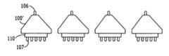
- a wafer (i.e., a substrate) 100has a thickness (t 1 ) of about 250 microns to about 400 microns.
- a plurality of light emitting devices (LED) 110are formed on a surface of the wafer 100 that is opposite a backside 103 of the wafer 100 .
- the plurality of LEDscan be GaN-based light emitting diodes that typically comprise an insulating or semiconducting substrate (or wafer) such as SiC or sapphire on which a plurality of GaN-based epitaxial layers are deposited.
- the epitaxial layerscomprise an active region having a p-n junction that emits light when energized.
- the waferis a SiC wafer of 4H—SIC, 6H—SiC or another type of material known to those skilled in the art.
- a wafer 100(including the plurality of LEDs 110 ) and a wafer carrier 105 are coupled together via an adhesive layer 120 in contact with the plurality of LEDs so that the entire assembly can be subject to processing by, for example, mounting the wafer carrier 105 in a grinder so that the backside 103 of the wafer 100 can be accessed.
- the wafer 100 /plurality of LEDs 110can be coupled to the wafer carrier 105 using any technique known to those skilled in the art, such as a wax, and may be applied to the plurality of LEDs or to the wafer carrier.
- contactincludes direct contact as well as indirect contact where, for example, one or more intervening elements (such as the adhesive layer described above) are present between the plurality of LEDs and the wafer so that these two elements can be coupled together and the backside of the wafer can be processed while holding the carrier.
- intervening elementssuch as the adhesive layer described above
- the backside 103 of the wafer 100is processed to reduce the wafer 100 to a thickness t 2 , which is less than t 1 , to form a thinned wafer 100 ′.
- the thickness t 2is less than t 1 to allow a saw blade having a beveled tip to cut beneath the surface of the backside 103 to a depth less than about a length of the bevel of the tip of the saw blade. Accordingly, the beveled tip is partially inserted into the backside 103 so that straight edges of the saw blade can remain exposed above the backside 103 .
- the thickness of the wafer 100is reduced using a grinder, such as an in-feed or creep feed grinder.
- a grindersuch as an in-feed or creep feed grinder.
- the thickness of the wafer 100is reduced using lapping, chemical or reactive ion etching or combinations of these approaches with or without grinding.
- etchingmay be used to treat the backside of the thinned wafer (i.e., after thinning the wafer) to reduce damage to the wafer so that growth of epi-layers may be improved.
- the beveled tipmay be inserted farther so that a small portion of the straight edges of the saw blade are inserted below the surface of the thinned wafer 100 ′.
- the LEDs so formedmay still provide the substantially the same benefits as those embodiments where the beveled tip is partially inserted (such as improved light extraction and improved conformal deposition of a phosphor coating thereon). Accordingly, embodiments where a small portion of the straight edges of the saw blade are inserted below the surface of the thinned wafer 100 ′ will be understood to be within the scope of the claimed subject matter.
- the wafer 100is thinned to a thickness of less than about 150 microns. In other embodiments according to the invention, the wafer 100 is thinned to a thickness of less than about 120 microns. In some embodiments according to the invention, the wafer 100 is thinned using an in-feed grinder or a creep-feed grinder.
- the wafer carrier 105can be removed from the assembly by, for example, heating the adhesive layer 120 so that the thinned wafer 100 ′ and the plurality of LEDs thereon may be removed as shown in FIG. 4 .
- the wafer carrier 105can be removed from the assembly using an appropriate based on the structure used to couple these elements as shown above in reference, for example, to FIG. 2 .
- the structuremay be dissolved or melted to separate the wafer carrier 105 from the assembly.
- Ohmic contacts 107can be formed on the backside 103 of the wafer 100 ′ using, for example, laser annealing as discussed in U.S. patent application Ser. No. 10/916,113, entitled Localized Annealing of Metal-Silicon Carbide Ohmic Contacts and Devices So Formed to Slater et al., filed Aug. 11, 2004, which is commonly assigned to the present Assignee, the disclosure of which is incorporated herein by reference. It will be understood that the ohmic contacts can be formed on the thinned wafer 100 ′ while the wafer is coupled to the wafer carrier.
- the ohmic contactscan be formed on the thinned wafer 100 ′ after the wafer is removed from the wafer carrier, as shown for example, in FIG. 5 .
- Bonding pads 106can be formed on the plurality of LEDs 110 opposite the ohmic contacts.
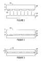
- a saw blade 30can be used to cut the wafer 100 ′ to separate the plurality of LEDs for packaging. It will be understood that the saw blade 30 can cut through the entire wafer 100 ′ to form straight edges on the thinned wafer 100 ′ between the separated plurality of LEDs 110 or substantially through the thinned wafer 100 ′ so that the LEDs 110 may be separated from one another by applying pressure along the score lines formed by the saw blade 30 .
- the saw blade 30is partially inserted into the thinned wafer 100 ′ to a depth that is less than the length of the beveled tip 131 to form beveled grooves 17 in the thinned wafer 100 ′.
- the saw 30is partially inserted into the thinned wafer 100 ′ so that the straight edges 31 of the saw 30 remain exposed when the beveled tip 131 is partially inserted to avoid the formation of undesirable geometries in the thinned wafer 100 ′ above the beveled grooves 17 .
- the thickness of the thinned wafer 100 ′allows the beveled groves 17 to penetrate sufficiently into the thinned wafer 110 ′ so that the plurality of LEDs can be separated from one another by breaking the thinned wafer 100 ′ along grooves (or score lines) as shown in FIG. 7 .
- bonding pads 106 and ohmic contacts 107can be formed on the plurality of LEDs.
- the backside 103 of the wafer 100 ′can be processed to further improve light extraction from the LED including patterning the backside 103 with a laser or by what is commonly referred to as “roughing.”
- the laser patterningmay be provided in a single or step-wise fashion.
- By patterning the backside 103light extraction may be improved, for example, by providing a randomization pattern thereon.
- Embodiments of the inventionmay be particularly well suited to larger area devices where the effectiveness of angled sidewalls of the wafer 100 ′ may be reduced because of the surface area of the device.
- one or both of the opposing faces of the wafer 100 ′i.e., a front side and the backside 103 ) may be patterned.
- the wafer 100 ′may be patterned using a laser patterning system such as that described in U.S. patent application Ser. No. 10/815,293, entitled Laser Patterning of Light Emitting Devices and Patterned Light Emitting Devices to Donofrio, filed Apr. 1, 2004, the entire disclosure of which is incorporated herein by reference.
- the laser used to pattern the wafer 100 ′is an excimer pulsed laser, however any laser system suitable for removing material from the substrate may be used.
- the laser systemcould be a frequency tripled and/or quadrupled YAG laser.
- the laserhas a wavelength of 308 nm, however, other wavelengths, such as 248 nm, 193 nm, 157 nm, 355 nm or 266 nm could also be used.
- assist processes known to those of skill in the artcould also be employed to mitigate surface damage and/or enhance laser absorption, such as water mist and/or assist gases.
- Multiple pulses of the lasermay be used to remove material from the substrate. Any energy suitable for controllably removing material from the substrate may be used. For example, a pulsed 308 nm laser of about 4.2 J/pulse may be used in certain embodiments of the present invention.
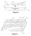
- FIG. 8is a cross-sectional view of an LED on the wafer 100 ′ having the backside 103 laser patterned according to some embodiments of the invention.
- FIG. 9is an isometric pictorial view of the light-emitting device of FIG. 8 .
- Three-dimensional patterns 120are formed in the backside 103 using a laser as described above.
- the LED 110is formed on an opposite side 104 (i.e., front side) of the wafer 100 ′.
- the patterns 120are surrounded by an uninterrupted perimeter 130 on the backside 103 of the wafer 100 .
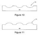
- FIGS. 10 and 11are cross-sectional views of wafers 100 ′ according to further embodiments of the present invention.
- curved surfaces extending into 200 or protruding 210 from the wafer 100 ′may be provided by laser patterning.
- the curved surfaces 200 , 210may include a parabolic curve. Such a curve may be provided, for example, by controlling the laser light using a series of masks that provided the selective removal of substrate material to provide the parabolic structures.
- the curved surfacesmay provide lenses in the substrate.
- the curved surfacesmay provide a sinusoidal pattern of grooves.
- the wafer 100 ′could be shaped to a single curve so as to provide a curved wafer 100 ′.
- the curved wafer 100 ′may be curved on both faces.
- the light emitting devicecould be provided on the curved surface of the wafer 100 ′.
- FIGS. 12 and 13are cross-sectional views of wafers 100 ′ according to further embodiments of the invention. As seen in FIGS. 12 and 13 , combinations of curved 220 and non-curved features 230 , 240 may be provided in a single wafer 100 ′. Thus, embodiments of the invention may include multiple different three-dimensional geometric patterns in a single wafer 100 ′.
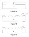
- FIGS. 14 through 16illustrate alternative embodiments for laser patterning according to some embodiments of the invention.
- a polymer mask layer 300may be provided on the wafer 100 ′.
- the polymer mask layer 300is laser patterned to provide a polymer mask 310 having three-dimensional features 320 corresponding to features to be provided in the wafer 100 ′.
- the mask 310is used as an etch mask and the wafer 100 ′ is etched to provide the three-dimensional features 330 .
- the etchmay, for example, be a dry etch.
- Conventional polymer masks and techniques for etching using polymer masksmay be used. Additionally, other mask materials that may be laser patterned could also be used.
- the etching maskis a polymer etching mask
- the polymermay be patterned with a 248 nm laser.
- Characteristics of the etching processmay be taken into account in designing the characteristics of the mask 310 to provide a desired three-dimensional geometric pattern in the wafer 100 ′. For example, the differences in etch rate between the mask material and the silicon carbide wafer may be taken into account when the mask is patterned.
- the shape of the etching maskmay be readily adjusted through control of the laser mask.
- the shape of the etching maskmay take into account the 6 to 1 etching rate of the etching mask to the silicon carbide and the features adjusted accordingly.
- Such an adjustment of mask characteristicsmay be difficult to provide without the use of laser patterning of the etching mask.
- multiple geometries, e.g., pyramids and lensescan be formed in a single step with scanning image technique by designing them into the laser mask.
- the surface of the wafer after the etchmay be rough or smooth.
- a roughened surfacemay be provided, for example, by placing a thin layer of material, such as aluminum, between the etch mask and the substrate to create a micro-mask. When etched, the micro-mask may act to roughen a surface of the wafer 100 ′.
Landscapes
- Led Devices (AREA)
Abstract
Description
Claims (25)
Priority Applications (6)
| Application Number | Priority Date | Filing Date | Title |
|---|---|---|---|
| CA002545628ACA2545628A1 (en) | 2003-11-12 | 2004-11-12 | Methods of processing semiconductor wafer backsides having light emitting devices (leds) thereon and leds so formed |
| PCT/US2004/037934WO2005048363A2 (en) | 2003-11-12 | 2004-11-12 | Methods of processing semiconductor wafer backsides having light emitting devices (leds) thereon and leds so formed |
| KR1020067011181AKR20060131774A (en) | 2003-11-12 | 2004-11-12 | Processing methods of the semiconductor wafer backsides having light emitting elements on semiconductor wafer backsides and light emitting elements formed by the methods |
| JP2006539938AJP2007511105A (en) | 2003-11-12 | 2004-11-12 | Method for processing the back side of a semiconductor wafer having a light emitting device (LED) thereon, and an LED formed by the method |
| EP04810913AEP1690301B1 (en) | 2003-11-12 | 2004-11-12 | Methods of processing semiconductor wafer backsides having light emitting diodes (leds) thereon |
| US10/987,135US7291529B2 (en) | 2003-11-12 | 2004-11-12 | Methods of processing semiconductor wafer backsides having light emitting devices (LEDs) thereon |
Applications Claiming Priority (2)
| Application Number | Priority Date | Filing Date | Title |
|---|---|---|---|
| US51939603P | 2003-11-12 | 2003-11-12 | |
| US10/987,135US7291529B2 (en) | 2003-11-12 | 2004-11-12 | Methods of processing semiconductor wafer backsides having light emitting devices (LEDs) thereon |
Publications (2)
| Publication Number | Publication Date |
|---|---|
| US20050151138A1 US20050151138A1 (en) | 2005-07-14 |
| US7291529B2true US7291529B2 (en) | 2007-11-06 |
Family
ID=34594959
Family Applications (1)
| Application Number | Title | Priority Date | Filing Date |
|---|---|---|---|
| US10/987,135Active2025-11-10US7291529B2 (en) | 2003-11-12 | 2004-11-12 | Methods of processing semiconductor wafer backsides having light emitting devices (LEDs) thereon |
Country Status (6)
| Country | Link |
|---|---|
| US (1) | US7291529B2 (en) |
| EP (1) | EP1690301B1 (en) |
| JP (1) | JP2007511105A (en) |
| KR (1) | KR20060131774A (en) |
| CA (1) | CA2545628A1 (en) |
| WO (1) | WO2005048363A2 (en) |
Cited By (18)
| Publication number | Priority date | Publication date | Assignee | Title |
|---|---|---|---|---|
| US20080203405A1 (en)* | 2005-08-05 | 2008-08-28 | Johannes Otto Rooymans | Method for Preparing an Electric Circuit Comprising Multiple Leds |
| US20100159620A1 (en)* | 2005-08-26 | 2010-06-24 | Seoul Semiconductor Co., Ltd. | Manufacturing method of light emitting diode |
| US7772604B2 (en) | 2006-01-05 | 2010-08-10 | Illumitex | Separate optical device for directing light from an LED |
| US7789531B2 (en) | 2006-10-02 | 2010-09-07 | Illumitex, Inc. | LED system and method |
| US7829358B2 (en) | 2008-02-08 | 2010-11-09 | Illumitex, Inc. | System and method for emitter layer shaping |
| US8115217B2 (en) | 2008-12-11 | 2012-02-14 | Illumitex, Inc. | Systems and methods for packaging light-emitting diode devices |
| US8449128B2 (en) | 2009-08-20 | 2013-05-28 | Illumitex, Inc. | System and method for a lens and phosphor layer |
| US8585253B2 (en) | 2009-08-20 | 2013-11-19 | Illumitex, Inc. | System and method for color mixing lens array |
| US8698183B2 (en) | 2006-09-25 | 2014-04-15 | Lg Innotek Co., Ltd. | Light emitting diode and method for manufacturing the same |
| US8921876B2 (en) | 2009-06-02 | 2014-12-30 | Cree, Inc. | Lighting devices with discrete lumiphor-bearing regions within or on a surface of remote elements |
| WO2020252234A1 (en) | 2019-06-13 | 2020-12-17 | Cree, Inc. | High electron mobility transistors and power amplifiers including said transistors having improved performance and reliability |
| US10923585B2 (en) | 2019-06-13 | 2021-02-16 | Cree, Inc. | High electron mobility transistors having improved contact spacing and/or improved contact vias |
| WO2021247276A2 (en) | 2020-06-01 | 2021-12-09 | Cree, Inc. | Methods for pillar connection on frontside and passive device integration on backside of die |
| WO2022245886A1 (en) | 2021-05-20 | 2022-11-24 | Wolfspeed, Inc. | Methods of manufacturing high electron mobility transistors having improved performance |
| WO2023009405A1 (en) | 2021-07-30 | 2023-02-02 | Wolfspeed, Inc. | Encapsulation stack on a transistor and fabrication method thereof |
| WO2023043524A1 (en) | 2021-09-16 | 2023-03-23 | Wolfspeed, Inc. | Semiconductor device incorporating a substrate recess |
| US12009417B2 (en) | 2021-05-20 | 2024-06-11 | Macom Technology Solutions Holdings, Inc. | High electron mobility transistors having improved performance |
| US12446252B2 (en) | 2021-05-20 | 2025-10-14 | Macom Technology Solutions Holdings, Inc. | Transistors including semiconductor surface modification and related fabrication methods |
Families Citing this family (43)
| Publication number | Priority date | Publication date | Assignee | Title |
|---|---|---|---|---|
| EP1690301B1 (en)* | 2003-11-12 | 2012-08-15 | Cree, Inc. | Methods of processing semiconductor wafer backsides having light emitting diodes (leds) thereon |
| US7419912B2 (en) | 2004-04-01 | 2008-09-02 | Cree, Inc. | Laser patterning of light emitting devices |
| WO2006031641A2 (en)* | 2004-09-10 | 2006-03-23 | Cree, Inc. | Method of manufacturing carrier wafer and resulting carrier wafer structures |
| DE102004061865A1 (en)* | 2004-09-29 | 2006-03-30 | Osram Opto Semiconductors Gmbh | Process for producing a thin-film semiconductor chip |
| EP2546865B1 (en)* | 2005-09-16 | 2023-12-06 | Wolfspeed, Inc. | Methods of processing semiconductor wafers having silicon carbide power devices thereon |
| US8264138B2 (en) | 2006-01-20 | 2012-09-11 | Cree, Inc. | Shifting spectral content in solid state light emitters by spatially separating lumiphor films |
| US8441179B2 (en) | 2006-01-20 | 2013-05-14 | Cree, Inc. | Lighting devices having remote lumiphors that are excited by lumiphor-converted semiconductor excitation sources |
| US8698184B2 (en) | 2011-01-21 | 2014-04-15 | Cree, Inc. | Light emitting diodes with low junction temperature and solid state backlight components including light emitting diodes with low junction temperature |
| US8432012B2 (en) | 2006-08-01 | 2013-04-30 | Cree, Inc. | Semiconductor devices including schottky diodes having overlapping doped regions and methods of fabricating same |
| US7728402B2 (en) | 2006-08-01 | 2010-06-01 | Cree, Inc. | Semiconductor devices including schottky diodes with controlled breakdown |
| KR101529331B1 (en) | 2006-08-17 | 2015-06-16 | 크리 인코포레이티드 | High power insulated gate bipolar transistors |
| EP2060155A2 (en) | 2006-08-23 | 2009-05-20 | Cree Led Lighting Solutions, Inc. | Lighting device and lighting method |
| US8835987B2 (en) | 2007-02-27 | 2014-09-16 | Cree, Inc. | Insulated gate bipolar transistors including current suppressing layers |
| US8866150B2 (en)* | 2007-05-31 | 2014-10-21 | Cree, Inc. | Silicon carbide power devices including P-type epitaxial layers and direct ohmic contacts |
| US7863635B2 (en) | 2007-08-07 | 2011-01-04 | Cree, Inc. | Semiconductor light emitting devices with applied wavelength conversion materials |
| US7687825B2 (en)* | 2007-09-18 | 2010-03-30 | Cree, Inc. | Insulated gate bipolar conduction transistors (IBCTS) and related methods of fabrication |
| JP2011501466A (en)* | 2007-10-26 | 2011-01-06 | クリー エル イー ディー ライティング ソリューションズ インコーポレイテッド | Lighting device having one or more light emitters and method of making the same |
| US8232558B2 (en) | 2008-05-21 | 2012-07-31 | Cree, Inc. | Junction barrier Schottky diodes with current surge capability |
| US8187983B2 (en)* | 2009-04-16 | 2012-05-29 | Micron Technology, Inc. | Methods for fabricating semiconductor components using thinning and back side laser processing |
| US8294507B2 (en) | 2009-05-08 | 2012-10-23 | Cree, Inc. | Wide bandgap bipolar turn-off thyristor having non-negative temperature coefficient and related control circuits |
| US8193848B2 (en) | 2009-06-02 | 2012-06-05 | Cree, Inc. | Power switching devices having controllable surge current capabilities |
| US8629509B2 (en) | 2009-06-02 | 2014-01-14 | Cree, Inc. | High voltage insulated gate bipolar transistors with minority carrier diverter |
| DE102009032486A1 (en)* | 2009-07-09 | 2011-01-13 | Osram Opto Semiconductors Gmbh | Optoelectronic component |
| US8541787B2 (en) | 2009-07-15 | 2013-09-24 | Cree, Inc. | High breakdown voltage wide band-gap MOS-gated bipolar junction transistors with avalanche capability |
| US8354690B2 (en) | 2009-08-31 | 2013-01-15 | Cree, Inc. | Solid-state pinch off thyristor circuits |
| US9275979B2 (en) | 2010-03-03 | 2016-03-01 | Cree, Inc. | Enhanced color rendering index emitter through phosphor separation |
| US9117739B2 (en) | 2010-03-08 | 2015-08-25 | Cree, Inc. | Semiconductor devices with heterojunction barrier regions and methods of fabricating same |
| US8415671B2 (en) | 2010-04-16 | 2013-04-09 | Cree, Inc. | Wide band-gap MOSFETs having a heterojunction under gate trenches thereof and related methods of forming such devices |
| DE102010027679A1 (en) | 2010-07-20 | 2012-01-26 | Osram Opto Semiconductors Gmbh | Optoelectronic component |
| JP5643036B2 (en)* | 2010-09-14 | 2014-12-17 | 株式会社ディスコ | Processing method of optical device wafer |
| US11251164B2 (en) | 2011-02-16 | 2022-02-15 | Creeled, Inc. | Multi-layer conversion material for down conversion in solid state lighting |
| TWI452691B (en)* | 2011-04-25 | 2014-09-11 | Univ Nat Cheng Kung | Semiconductor structure and method for making the same, and method for forming epitaxial semi-finished product |
| US9142662B2 (en) | 2011-05-06 | 2015-09-22 | Cree, Inc. | Field effect transistor devices with low source resistance |
| US9673283B2 (en) | 2011-05-06 | 2017-06-06 | Cree, Inc. | Power module for supporting high current densities |
| US9029945B2 (en) | 2011-05-06 | 2015-05-12 | Cree, Inc. | Field effect transistor devices with low source resistance |
| US9640617B2 (en) | 2011-09-11 | 2017-05-02 | Cree, Inc. | High performance power module |
| US8618582B2 (en) | 2011-09-11 | 2013-12-31 | Cree, Inc. | Edge termination structure employing recesses for edge termination elements |
| US8680587B2 (en) | 2011-09-11 | 2014-03-25 | Cree, Inc. | Schottky diode |
| US8664665B2 (en) | 2011-09-11 | 2014-03-04 | Cree, Inc. | Schottky diode employing recesses for elements of junction barrier array |
| US9373617B2 (en) | 2011-09-11 | 2016-06-21 | Cree, Inc. | High current, low switching loss SiC power module |
| JP2014011244A (en)* | 2012-06-28 | 2014-01-20 | Nitto Denko Corp | Led manufacturing method |
| US20190237644A1 (en)* | 2018-01-30 | 2019-08-01 | Mikro Mesa Technology Co., Ltd. | Light emitting device with multi-layer isolation structure |
| WO2024240564A1 (en)* | 2023-05-25 | 2024-11-28 | Ams-Osram International Gmbh | Optoelectronic semiconductor chip and corresponding production method |
Citations (32)
| Publication number | Priority date | Publication date | Assignee | Title |
|---|---|---|---|---|
| US4918497A (en) | 1988-12-14 | 1990-04-17 | Cree Research, Inc. | Blue light emitting diode formed in silicon carbide |
| US4966862A (en) | 1989-08-28 | 1990-10-30 | Cree Research, Inc. | Method of production of light emitting diodes |
| US5027168A (en) | 1988-12-14 | 1991-06-25 | Cree Research, Inc. | Blue light emitting diode formed in silicon carbide |
| US5087949A (en) | 1989-06-27 | 1992-02-11 | Hewlett-Packard Company | Light-emitting diode with diagonal faces |
| US5210051A (en) | 1990-03-27 | 1993-05-11 | Cree Research, Inc. | High efficiency light emitting diodes from bipolar gallium nitride |
| US5338944A (en) | 1993-09-22 | 1994-08-16 | Cree Research, Inc. | Blue light-emitting diode with degenerate junction structure |
| US5393993A (en) | 1993-12-13 | 1995-02-28 | Cree Research, Inc. | Buffer structure between silicon carbide and gallium nitride and resulting semiconductor devices |
| US5416342A (en) | 1993-06-23 | 1995-05-16 | Cree Research, Inc. | Blue light-emitting diode with high external quantum efficiency |
| US5523589A (en) | 1994-09-20 | 1996-06-04 | Cree Research, Inc. | Vertical geometry light emitting diode with group III nitride active layer and extended lifetime |
| US5604135A (en) | 1994-08-12 | 1997-02-18 | Cree Research, Inc. | Method of forming green light emitting diode in silicon carbide |
| US5631190A (en) | 1994-10-07 | 1997-05-20 | Cree Research, Inc. | Method for producing high efficiency light-emitting diodes and resulting diode structures |
| US5739554A (en) | 1995-05-08 | 1998-04-14 | Cree Research, Inc. | Double heterojunction light emitting diode with gallium nitride active layer |
| US5994205A (en) | 1997-02-03 | 1999-11-30 | Kabushiki Kaisha Toshiba | Method of separating semiconductor devices |
| JP2000022213A (en) | 1998-06-30 | 2000-01-21 | Sharp Corp | Gallium nitride based semiconductor device and manufacturing method thereof |
| US6187606B1 (en) | 1997-10-07 | 2001-02-13 | Cree, Inc. | Group III nitride photonic devices on silicon carbide substrates with conductive buffer interlayer structure |
| US6197609B1 (en)* | 1998-09-07 | 2001-03-06 | Rohm Co., Ltd. | Method for manufacturing semiconductor light emitting device |
| US20020076904A1 (en)* | 2000-12-20 | 2002-06-20 | Imler William R. | Separation method for gallium nitride devices on lattice-mismatched substrates |
| US20020113235A1 (en)* | 2001-02-20 | 2002-08-22 | Showa Denko K.K. | Group-III nitride semiconductor light-emitting diode |
| US20020123164A1 (en)* | 2001-02-01 | 2002-09-05 | Slater David B. | Light emitting diodes including modifications for light extraction and manufacturing methods therefor |
| WO2002082502A2 (en) | 2001-04-03 | 2002-10-17 | Commissariat A L'energie Atomique | Method for selectively transferring at least an element from an initial support onto a final support |
| US20020179910A1 (en)* | 2001-03-15 | 2002-12-05 | Slater David B. | Low temperature formation of backside ohmic contacts for vertical devices |
| US20030006418A1 (en) | 2001-05-30 | 2003-01-09 | Emerson David Todd | Group III nitride based light emitting diode structures with a quantum well and superlattice, group III nitride based quantum well structures and group III nitride based superlattice structures |
| US20030168663A1 (en)* | 2001-02-01 | 2003-09-11 | Slater David B. | Reflective ohmic contacts for silicon carbide including a layer consisting essentially of nickel, methods of fabricating same, and light emitting devices including the same |
| US6649017B1 (en)* | 1999-09-06 | 2003-11-18 | Lintec Corporation | Method of detaching article fixed through pressure sensitive adhesive double coated sheet |
| US20040056260A1 (en) | 2002-09-19 | 2004-03-25 | Slater David B. | Phosphor-coated light emitting diodes including tapered sidewalls, and fabrication methods therefor |
| US6740906B2 (en)* | 2001-07-23 | 2004-05-25 | Cree, Inc. | Light emitting diodes including modifications for submount bonding |
| US20040171204A1 (en)* | 2001-03-15 | 2004-09-02 | Slater David B. | Low temperature formation of backside ohmic contacts for vertical devices |
| US6818532B2 (en)* | 2002-04-09 | 2004-11-16 | Oriol, Inc. | Method of etching substrates |
| US6869819B2 (en)* | 2002-05-28 | 2005-03-22 | Fujitsu Limited | Recognition method of a mark provided on a semiconductor device |
| US6884644B1 (en)* | 1998-09-16 | 2005-04-26 | Cree, Inc. | Low temperature formation of backside ohmic contacts for vertical devices |
| US20050104072A1 (en)* | 2003-08-14 | 2005-05-19 | Slater David B.Jr. | Localized annealing of metal-silicon carbide ohmic contacts and devices so formed |
| US20050151138A1 (en)* | 2003-11-12 | 2005-07-14 | Slater David B.Jr. | Methods of processing semiconductor wafer backsides having light emitting devices (LEDS) thereon and leds so formed |
Family Cites Families (7)
| Publication number | Priority date | Publication date | Assignee | Title |
|---|---|---|---|---|
| EP0405757A3 (en)* | 1989-06-27 | 1991-01-30 | Hewlett-Packard Company | High efficiency light-emitting diode |
| JP2914014B2 (en)* | 1992-06-05 | 1999-06-28 | 日亜化学工業株式会社 | Method of manufacturing gallium nitride based compound semiconductor chip |
| US6459100B1 (en)* | 1998-09-16 | 2002-10-01 | Cree, Inc. | Vertical geometry ingan LED |
| TW465123B (en)* | 2000-02-02 | 2001-11-21 | Ind Tech Res Inst | High power white light LED |
| JP2002319708A (en)* | 2001-04-23 | 2002-10-31 | Matsushita Electric Works Ltd | Led chip and led device |
| JP4244542B2 (en)* | 2001-08-28 | 2009-03-25 | 日亜化学工業株式会社 | Gallium nitride compound semiconductor light emitting device and method for manufacturing the same |
| US6635503B2 (en)* | 2002-01-28 | 2003-10-21 | Cree, Inc. | Cluster packaging of light emitting diodes |
- 2004
- 2004-11-12EPEP04810913Apatent/EP1690301B1/ennot_activeExpired - Lifetime
- 2004-11-12WOPCT/US2004/037934patent/WO2005048363A2/enactiveApplication Filing
- 2004-11-12JPJP2006539938Apatent/JP2007511105A/enactivePending
- 2004-11-12CACA002545628Apatent/CA2545628A1/ennot_activeAbandoned
- 2004-11-12USUS10/987,135patent/US7291529B2/enactiveActive
- 2004-11-12KRKR1020067011181Apatent/KR20060131774A/ennot_activeWithdrawn
Patent Citations (43)
| Publication number | Priority date | Publication date | Assignee | Title |
|---|---|---|---|---|
| US4918497A (en) | 1988-12-14 | 1990-04-17 | Cree Research, Inc. | Blue light emitting diode formed in silicon carbide |
| US5027168A (en) | 1988-12-14 | 1991-06-25 | Cree Research, Inc. | Blue light emitting diode formed in silicon carbide |
| US5087949A (en) | 1989-06-27 | 1992-02-11 | Hewlett-Packard Company | Light-emitting diode with diagonal faces |
| US4966862A (en) | 1989-08-28 | 1990-10-30 | Cree Research, Inc. | Method of production of light emitting diodes |
| US5210051A (en) | 1990-03-27 | 1993-05-11 | Cree Research, Inc. | High efficiency light emitting diodes from bipolar gallium nitride |
| US5416342A (en) | 1993-06-23 | 1995-05-16 | Cree Research, Inc. | Blue light-emitting diode with high external quantum efficiency |
| US5338944A (en) | 1993-09-22 | 1994-08-16 | Cree Research, Inc. | Blue light-emitting diode with degenerate junction structure |
| US5393993A (en) | 1993-12-13 | 1995-02-28 | Cree Research, Inc. | Buffer structure between silicon carbide and gallium nitride and resulting semiconductor devices |
| US5604135A (en) | 1994-08-12 | 1997-02-18 | Cree Research, Inc. | Method of forming green light emitting diode in silicon carbide |
| US5523589A (en) | 1994-09-20 | 1996-06-04 | Cree Research, Inc. | Vertical geometry light emitting diode with group III nitride active layer and extended lifetime |
| US5631190A (en) | 1994-10-07 | 1997-05-20 | Cree Research, Inc. | Method for producing high efficiency light-emitting diodes and resulting diode structures |
| US5912477A (en) | 1994-10-07 | 1999-06-15 | Cree Research, Inc. | High efficiency light emitting diodes |
| US5739554A (en) | 1995-05-08 | 1998-04-14 | Cree Research, Inc. | Double heterojunction light emitting diode with gallium nitride active layer |
| US6120600A (en) | 1995-05-08 | 2000-09-19 | Cree, Inc. | Double heterojunction light emitting diode with gallium nitride active layer |
| US5994205A (en) | 1997-02-03 | 1999-11-30 | Kabushiki Kaisha Toshiba | Method of separating semiconductor devices |
| US6187606B1 (en) | 1997-10-07 | 2001-02-13 | Cree, Inc. | Group III nitride photonic devices on silicon carbide substrates with conductive buffer interlayer structure |
| US6201262B1 (en) | 1997-10-07 | 2001-03-13 | Cree, Inc. | Group III nitride photonic devices on silicon carbide substrates with conductive buffer interlay structure |
| JP2000022213A (en) | 1998-06-30 | 2000-01-21 | Sharp Corp | Gallium nitride based semiconductor device and manufacturing method thereof |
| US6197609B1 (en)* | 1998-09-07 | 2001-03-06 | Rohm Co., Ltd. | Method for manufacturing semiconductor light emitting device |
| US6884644B1 (en)* | 1998-09-16 | 2005-04-26 | Cree, Inc. | Low temperature formation of backside ohmic contacts for vertical devices |
| US6649017B1 (en)* | 1999-09-06 | 2003-11-18 | Lintec Corporation | Method of detaching article fixed through pressure sensitive adhesive double coated sheet |
| US20020076904A1 (en)* | 2000-12-20 | 2002-06-20 | Imler William R. | Separation method for gallium nitride devices on lattice-mismatched substrates |
| US6791119B2 (en)* | 2001-02-01 | 2004-09-14 | Cree, Inc. | Light emitting diodes including modifications for light extraction |
| US20020123164A1 (en)* | 2001-02-01 | 2002-09-05 | Slater David B. | Light emitting diodes including modifications for light extraction and manufacturing methods therefor |
| US20060131599A1 (en)* | 2001-02-01 | 2006-06-22 | Cree, Inc. | Light emitting diodes including pedestals |
| US20030168663A1 (en)* | 2001-02-01 | 2003-09-11 | Slater David B. | Reflective ohmic contacts for silicon carbide including a layer consisting essentially of nickel, methods of fabricating same, and light emitting devices including the same |
| US7026659B2 (en)* | 2001-02-01 | 2006-04-11 | Cree, Inc. | Light emitting diodes including pedestals |
| US20040217362A1 (en)* | 2001-02-01 | 2004-11-04 | Slater David B | Light emitting diodes including pedestals |
| US6794684B2 (en)* | 2001-02-01 | 2004-09-21 | Cree, Inc. | Reflective ohmic contacts for silicon carbide including a layer consisting essentially of nickel, methods of fabricating same, and light emitting devices including the same |
| US20020113235A1 (en)* | 2001-02-20 | 2002-08-22 | Showa Denko K.K. | Group-III nitride semiconductor light-emitting diode |
| US6909119B2 (en)* | 2001-03-15 | 2005-06-21 | Cree, Inc. | Low temperature formation of backside ohmic contacts for vertical devices |
| US20040171204A1 (en)* | 2001-03-15 | 2004-09-02 | Slater David B. | Low temperature formation of backside ohmic contacts for vertical devices |
| US6803243B2 (en)* | 2001-03-15 | 2004-10-12 | Cree, Inc. | Low temperature formation of backside ohmic contacts for vertical devices |
| US20020179910A1 (en)* | 2001-03-15 | 2002-12-05 | Slater David B. | Low temperature formation of backside ohmic contacts for vertical devices |
| WO2002082502A2 (en) | 2001-04-03 | 2002-10-17 | Commissariat A L'energie Atomique | Method for selectively transferring at least an element from an initial support onto a final support |
| US20030006418A1 (en) | 2001-05-30 | 2003-01-09 | Emerson David Todd | Group III nitride based light emitting diode structures with a quantum well and superlattice, group III nitride based quantum well structures and group III nitride based superlattice structures |
| US6740906B2 (en)* | 2001-07-23 | 2004-05-25 | Cree, Inc. | Light emitting diodes including modifications for submount bonding |
| US7037742B2 (en)* | 2001-07-23 | 2006-05-02 | Cree, Inc. | Methods of fabricating light emitting devices using mesa regions and passivation layers |
| US6818532B2 (en)* | 2002-04-09 | 2004-11-16 | Oriol, Inc. | Method of etching substrates |
| US6869819B2 (en)* | 2002-05-28 | 2005-03-22 | Fujitsu Limited | Recognition method of a mark provided on a semiconductor device |
| US20040056260A1 (en) | 2002-09-19 | 2004-03-25 | Slater David B. | Phosphor-coated light emitting diodes including tapered sidewalls, and fabrication methods therefor |
| US20050104072A1 (en)* | 2003-08-14 | 2005-05-19 | Slater David B.Jr. | Localized annealing of metal-silicon carbide ohmic contacts and devices so formed |
| US20050151138A1 (en)* | 2003-11-12 | 2005-07-14 | Slater David B.Jr. | Methods of processing semiconductor wafer backsides having light emitting devices (LEDS) thereon and leds so formed |
Non-Patent Citations (4)
| Title |
|---|
| Boehlen et al., "Laser micro-machining of high density optical structures on large substrates," Exitech Ltd., Admitted Prior Art, 2004. |
| International Search Report and the Written Opinion of the International Searching Authority for International patent application PCT/US2004/037934 mailed on Jul. 13, 2005. |
| U.S. Appl. No. 10/815,293, filed Apr. 1, 2004, Donofrio. |
| U.S. Appl. No. 60/495,189, filed Aug. 11, 2004, Slater, Jr. et al. |
Cited By (35)
| Publication number | Priority date | Publication date | Assignee | Title |
|---|---|---|---|---|
| US20080203405A1 (en)* | 2005-08-05 | 2008-08-28 | Johannes Otto Rooymans | Method for Preparing an Electric Circuit Comprising Multiple Leds |
| US20100159620A1 (en)* | 2005-08-26 | 2010-06-24 | Seoul Semiconductor Co., Ltd. | Manufacturing method of light emitting diode |
| US8053259B2 (en)* | 2005-08-26 | 2011-11-08 | Seoul Semiconductor Co., Ltd. | Manufacturing method of light emitting diode |
| US7772604B2 (en) | 2006-01-05 | 2010-08-10 | Illumitex | Separate optical device for directing light from an LED |
| US7968896B2 (en) | 2006-01-05 | 2011-06-28 | Illumitex, Inc. | Separate optical device for directing light from an LED |
| US8896003B2 (en) | 2006-01-05 | 2014-11-25 | Illumitex, Inc. | Separate optical device for directing light from an LED |
| US9574743B2 (en) | 2006-01-05 | 2017-02-21 | Illumitex, Inc. | Separate optical device for directing light from an LED |
| US8698183B2 (en) | 2006-09-25 | 2014-04-15 | Lg Innotek Co., Ltd. | Light emitting diode and method for manufacturing the same |
| US8912565B2 (en) | 2006-09-25 | 2014-12-16 | Lg Innotek, Co., Ltd. | Light emitting diode and method for manufacturing the same |
| US9105761B2 (en) | 2006-09-25 | 2015-08-11 | Lg Innotek Co., Ltd. | Light emitting diode and method for manufacturing the same |
| US7789531B2 (en) | 2006-10-02 | 2010-09-07 | Illumitex, Inc. | LED system and method |
| US8087960B2 (en) | 2006-10-02 | 2012-01-03 | Illumitex, Inc. | LED system and method |
| US7829358B2 (en) | 2008-02-08 | 2010-11-09 | Illumitex, Inc. | System and method for emitter layer shaping |
| US8263993B2 (en) | 2008-02-08 | 2012-09-11 | Illumitex, Inc. | System and method for emitter layer shaping |
| US8115217B2 (en) | 2008-12-11 | 2012-02-14 | Illumitex, Inc. | Systems and methods for packaging light-emitting diode devices |
| US8921876B2 (en) | 2009-06-02 | 2014-12-30 | Cree, Inc. | Lighting devices with discrete lumiphor-bearing regions within or on a surface of remote elements |
| US9086211B2 (en) | 2009-08-20 | 2015-07-21 | Illumitex, Inc. | System and method for color mixing lens array |
| US8585253B2 (en) | 2009-08-20 | 2013-11-19 | Illumitex, Inc. | System and method for color mixing lens array |
| US8449128B2 (en) | 2009-08-20 | 2013-05-28 | Illumitex, Inc. | System and method for a lens and phosphor layer |
| US11616136B2 (en) | 2019-06-13 | 2023-03-28 | Wolfspeed, Inc. | High electron mobility transistors and power amplifiers including said transistors having improved performance and reliability |
| US10923585B2 (en) | 2019-06-13 | 2021-02-16 | Cree, Inc. | High electron mobility transistors having improved contact spacing and/or improved contact vias |
| US10971612B2 (en) | 2019-06-13 | 2021-04-06 | Cree, Inc. | High electron mobility transistors and power amplifiers including said transistors having improved performance and reliability |
| WO2020252234A1 (en) | 2019-06-13 | 2020-12-17 | Cree, Inc. | High electron mobility transistors and power amplifiers including said transistors having improved performance and reliability |
| WO2021247276A2 (en) | 2020-06-01 | 2021-12-09 | Cree, Inc. | Methods for pillar connection on frontside and passive device integration on backside of die |
| US11769768B2 (en) | 2020-06-01 | 2023-09-26 | Wolfspeed, Inc. | Methods for pillar connection on frontside and passive device integration on backside of die |
| US11842997B2 (en) | 2020-06-01 | 2023-12-12 | Wolfspeed, Inc. | Methods for pillar connection on frontside and passive device integration on backside of die |
| WO2022245886A1 (en) | 2021-05-20 | 2022-11-24 | Wolfspeed, Inc. | Methods of manufacturing high electron mobility transistors having improved performance |
| US12446252B2 (en) | 2021-05-20 | 2025-10-14 | Macom Technology Solutions Holdings, Inc. | Transistors including semiconductor surface modification and related fabrication methods |
| US12015075B2 (en) | 2021-05-20 | 2024-06-18 | Macom Technology Solutions Holdings, Inc. | Methods of manufacturing high electron mobility transistors having a modified interface region |
| US12009417B2 (en) | 2021-05-20 | 2024-06-11 | Macom Technology Solutions Holdings, Inc. | High electron mobility transistors having improved performance |
| US11842937B2 (en) | 2021-07-30 | 2023-12-12 | Wolfspeed, Inc. | Encapsulation stack for improved humidity performance and related fabrication methods |
| DE112022003795T5 (en) | 2021-07-30 | 2024-06-27 | Wolfspeed, Inc. | ENCAPSULATION STACK ON A TRANSISTOR AND MANUFACTURING METHOD THEREFOR |
| WO2023009405A1 (en) | 2021-07-30 | 2023-02-02 | Wolfspeed, Inc. | Encapsulation stack on a transistor and fabrication method thereof |
| WO2023043524A1 (en) | 2021-09-16 | 2023-03-23 | Wolfspeed, Inc. | Semiconductor device incorporating a substrate recess |
| US12218202B2 (en) | 2021-09-16 | 2025-02-04 | Wolfspeed, Inc. | Semiconductor device incorporating a substrate recess |
Also Published As
| Publication number | Publication date |
|---|---|
| WO2005048363A2 (en) | 2005-05-26 |
| JP2007511105A (en) | 2007-04-26 |
| CA2545628A1 (en) | 2005-05-26 |
| EP1690301A2 (en) | 2006-08-16 |
| US20050151138A1 (en) | 2005-07-14 |
| KR20060131774A (en) | 2006-12-20 |
| WO2005048363A3 (en) | 2005-09-15 |
| EP1690301B1 (en) | 2012-08-15 |
Similar Documents
| Publication | Publication Date | Title |
|---|---|---|
| US7291529B2 (en) | Methods of processing semiconductor wafer backsides having light emitting devices (LEDs) thereon | |
| TWI402997B (en) | Local annealing of metal-carbonized bismuth contact and device formed thereby | |
| US8877611B2 (en) | Devices with crack stops | |
| EP2546865B1 (en) | Methods of processing semiconductor wafers having silicon carbide power devices thereon | |
| US8211781B2 (en) | Semiconductor manufacturing method | |
| US8216867B2 (en) | Front end scribing of light emitting diode (LED) wafers and resulting devices | |
| CN102203966B (en) | Method for manufacturing semiconductor light-emitting element | |
| TWI254468B (en) | Compound semiconductor light-emitting device and production method thereof | |
| JP5130435B2 (en) | Group III nitride semiconductor substrate pattern forming method and group III nitride semiconductor light emitting device manufacturing method | |
| TW201025683A (en) | Series connected flip chip LEDs with growth substrate removed | |
| EP1935037B1 (en) | Group iii nitride semiconductor light-emitting device manufacturing method | |
| TW200525784A (en) | Methods of processing semiconductor wafer backsides having light emitting devices(LEDs) thereon and LEDs so formed |
Legal Events
| Date | Code | Title | Description |
|---|---|---|---|
| AS | Assignment | Owner name:CREE, INC., NORTH CAROLINA Free format text:ASSIGNMENT OF ASSIGNORS INTEREST;ASSIGNORS:SLATER, DAVID BEARDSLEY;DONOFRIO, MATTHEW;REEL/FRAME:015988/0084;SIGNING DATES FROM 20050203 TO 20050215 | |
| STCF | Information on status: patent grant | Free format text:PATENTED CASE | |
| FPAY | Fee payment | Year of fee payment:4 | |
| FPAY | Fee payment | Year of fee payment:8 | |
| MAFP | Maintenance fee payment | Free format text:PAYMENT OF MAINTENANCE FEE, 12TH YEAR, LARGE ENTITY (ORIGINAL EVENT CODE: M1553); ENTITY STATUS OF PATENT OWNER: LARGE ENTITY Year of fee payment:12 | |
| AS | Assignment | Owner name:CREE LED, INC., CALIFORNIA Free format text:ASSIGNMENT OF ASSIGNORS INTEREST;ASSIGNOR:CREE, INC.;REEL/FRAME:056012/0200 Effective date:20210301 | |
| AS | Assignment | Owner name:CITIZENS BANK, N.A., MASSACHUSETTS Free format text:SECURITY INTEREST;ASSIGNORS:SMART MODULAR TECHNOLOGIES, INC.;SMART HIGH RELIABILITY SOLUTIONS, LLC;SMART EMBEDDED COMPUTING, INC.;AND OTHERS;REEL/FRAME:058983/0001 Effective date:20220207 | |
| AS | Assignment | Owner name:SMART MODULAR TECHNOLOGIES, INC., CALIFORNIA Free format text:RELEASE OF PATENT SECURITY INTEREST RECORDED AT R/F 058983/0001;ASSIGNOR:CITIZENS BANK, N.A.;REEL/FRAME:071725/0207 Effective date:20250624 Owner name:SMART EMBEDDED COMPUTING, INC., ARIZONA Free format text:RELEASE OF PATENT SECURITY INTEREST RECORDED AT R/F 058983/0001;ASSIGNOR:CITIZENS BANK, N.A.;REEL/FRAME:071725/0207 Effective date:20250624 Owner name:SMART HIGH RELIABILITY SOLUTIONS LLC, CALIFORNIA Free format text:RELEASE OF PATENT SECURITY INTEREST RECORDED AT R/F 058983/0001;ASSIGNOR:CITIZENS BANK, N.A.;REEL/FRAME:071725/0207 Effective date:20250624 Owner name:CREELED, INC., CALIFORNIA Free format text:RELEASE OF PATENT SECURITY INTEREST RECORDED AT R/F 058983/0001;ASSIGNOR:CITIZENS BANK, N.A.;REEL/FRAME:071725/0207 Effective date:20250624 | |
| AS | Assignment | Owner name:JPMORGAN CHASE BANK, N.A., ILLINOIS Free format text:PATENT SECURITY AGREEMENT;ASSIGNORS:CREELED, INC.;PENGUIN SOLUTIONS CORPORATION (DE);SMART EMBEDDED COMPUTING, INC.;AND OTHERS;REEL/FRAME:071755/0001 Effective date:20250624 | |
| AS | Assignment | Owner name:CREELED, INC., CALIFORNIA Free format text:CORRECTIVE ASSIGNMENT TO CORRECT THE NAME OF THE ASSIGNEE PREVIOUSLY RECORDED ON REEL 56012 FRAME 200. ASSIGNOR(S) HEREBY CONFIRMS THE ASSIGNMENT;ASSIGNOR:CREE, INC.;REEL/FRAME:071874/0001 Effective date:20210301 |