US7289329B2 - Integration of planar transformer and/or planar inductor with power switches in power converter - Google Patents
Integration of planar transformer and/or planar inductor with power switches in power converterDownload PDFInfo
- Publication number
- US7289329B2 US7289329B2US10/964,000US96400004AUS7289329B2US 7289329 B2US7289329 B2US 7289329B2US 96400004 AUS96400004 AUS 96400004AUS 7289329 B2US7289329 B2US 7289329B2
- Authority
- US
- United States
- Prior art keywords
- layer
- electrically
- thermally conductive
- conductive layers
- substrate
- Prior art date
- Legal status (The legal status is an assumption and is not a legal conclusion. Google has not performed a legal analysis and makes no representation as to the accuracy of the status listed.)
- Expired - Lifetime, expires
Links
- 230000010354integrationEffects0.000titledescription4
- 239000000758substrateSubstances0.000claimsabstractdescription199
- 239000004065semiconductorSubstances0.000claimsabstractdescription160
- 238000004804windingMethods0.000claimsdescription67
- 239000004020conductorSubstances0.000claimsdescription32
- 238000000034methodMethods0.000claimsdescription21
- 230000008878couplingEffects0.000claimsdescription15
- 238000010168coupling processMethods0.000claimsdescription15
- 238000005859coupling reactionMethods0.000claimsdescription15
- 229910000679solderInorganic materials0.000claimsdescription13
- 238000005476solderingMethods0.000claimsdescription13
- 229910052751metalInorganic materials0.000claimsdescription7
- 239000002184metalSubstances0.000claimsdescription7
- RYGMFSIKBFXOCR-UHFFFAOYSA-NCopperChemical compound[Cu]RYGMFSIKBFXOCR-UHFFFAOYSA-N0.000claimsdescription6
- 229910052802copperInorganic materials0.000claimsdescription6
- 239000010949copperSubstances0.000claimsdescription6
- 239000012530fluidSubstances0.000claimsdescription5
- 239000002826coolantSubstances0.000claimsdescription4
- 238000000059patterningMethods0.000claimsdescription4
- 238000004891communicationMethods0.000claims2
- 239000007788liquidSubstances0.000claims1
- 239000003990capacitorSubstances0.000description6
- 239000000853adhesiveSubstances0.000description4
- 230000001070adhesive effectEffects0.000description4
- 238000003491arrayMethods0.000description4
- 239000000919ceramicSubstances0.000description4
- 238000010438heat treatmentMethods0.000description4
- 239000012761high-performance materialSubstances0.000description4
- 238000004519manufacturing processMethods0.000description4
- 230000007935neutral effectEffects0.000description4
- 230000010363phase shiftEffects0.000description4
- 230000009977dual effectEffects0.000description3
- 229920002799BoPETPolymers0.000description2
- 239000004593EpoxySubstances0.000description2
- 229910052581Si3N4Inorganic materials0.000description2
- 229910052782aluminiumInorganic materials0.000description2
- XAGFODPZIPBFFR-UHFFFAOYSA-NaluminiumChemical compound[Al]XAGFODPZIPBFFR-UHFFFAOYSA-N0.000description2
- PNEYBMLMFCGWSK-UHFFFAOYSA-Naluminium oxideInorganic materials[O-2].[O-2].[O-2].[Al+3].[Al+3]PNEYBMLMFCGWSK-UHFFFAOYSA-N0.000description2
- 238000010276constructionMethods0.000description2
- PMHQVHHXPFUNSP-UHFFFAOYSA-Mcopper(1+);methylsulfanylmethane;bromideChemical compoundBr[Cu].CSCPMHQVHHXPFUNSP-UHFFFAOYSA-M0.000description2
- 238000004146energy storageMethods0.000description2
- 230000005669field effectEffects0.000description2
- 239000000446fuelSubstances0.000description2
- 238000007726management methodMethods0.000description2
- 239000000463materialSubstances0.000description2
- 229910044991metal oxideInorganic materials0.000description2
- 150000004706metal oxidesChemical class0.000description2
- 229920003223poly(pyromellitimide-1,4-diphenyl ether)Polymers0.000description2
- 229920001721polyimidePolymers0.000description2
- 230000001172regenerating effectEffects0.000description2
- 230000001105regulatory effectEffects0.000description2
- HQVNEWCFYHHQES-UHFFFAOYSA-Nsilicon nitrideChemical compoundN12[Si]34N5[Si]62N3[Si]51N64HQVNEWCFYHHQES-UHFFFAOYSA-N0.000description2
- 230000035882stressEffects0.000description2
- 239000002470thermal conductorSubstances0.000description2
- 230000002411adverseEffects0.000description1
- 238000006243chemical reactionMethods0.000description1
- 230000001276controlling effectEffects0.000description1
- 238000005336crackingMethods0.000description1
- 230000007547defectEffects0.000description1
- 238000010586diagramMethods0.000description1
- 238000009826distributionMethods0.000description1
- 230000000694effectsEffects0.000description1
- 238000002955isolationMethods0.000description1
- 238000005259measurementMethods0.000description1
- 238000012986modificationMethods0.000description1
- 230000004048modificationEffects0.000description1
- 230000001360synchronised effectEffects0.000description1
- 230000008646thermal stressEffects0.000description1
Images


Classifications
- H—ELECTRICITY
- H01—ELECTRIC ELEMENTS
- H01F—MAGNETS; INDUCTANCES; TRANSFORMERS; SELECTION OF MATERIALS FOR THEIR MAGNETIC PROPERTIES
- H01F27/00—Details of transformers or inductances, in general
- H01F27/28—Coils; Windings; Conductive connections
- H01F27/2804—Printed windings
- H—ELECTRICITY
- H01—ELECTRIC ELEMENTS
- H01F—MAGNETS; INDUCTANCES; TRANSFORMERS; SELECTION OF MATERIALS FOR THEIR MAGNETIC PROPERTIES
- H01F27/00—Details of transformers or inductances, in general
- H01F27/08—Cooling; Ventilating
- H01F27/22—Cooling by heat conduction through solid or powdered fillings
- H—ELECTRICITY
- H01—ELECTRIC ELEMENTS
- H01F—MAGNETS; INDUCTANCES; TRANSFORMERS; SELECTION OF MATERIALS FOR THEIR MAGNETIC PROPERTIES
- H01F27/00—Details of transformers or inductances, in general
- H01F27/28—Coils; Windings; Conductive connections
- H—ELECTRICITY
- H02—GENERATION; CONVERSION OR DISTRIBUTION OF ELECTRIC POWER
- H02M—APPARATUS FOR CONVERSION BETWEEN AC AND AC, BETWEEN AC AND DC, OR BETWEEN DC AND DC, AND FOR USE WITH MAINS OR SIMILAR POWER SUPPLY SYSTEMS; CONVERSION OF DC OR AC INPUT POWER INTO SURGE OUTPUT POWER; CONTROL OR REGULATION THEREOF
- H02M7/00—Conversion of AC power input into DC power output; Conversion of DC power input into AC power output
- H—ELECTRICITY
- H05—ELECTRIC TECHNIQUES NOT OTHERWISE PROVIDED FOR
- H05K—PRINTED CIRCUITS; CASINGS OR CONSTRUCTIONAL DETAILS OF ELECTRIC APPARATUS; MANUFACTURE OF ASSEMBLAGES OF ELECTRICAL COMPONENTS
- H05K7/00—Constructional details common to different types of electric apparatus
- H05K7/20—Modifications to facilitate cooling, ventilating, or heating
- H—ELECTRICITY
- H01—ELECTRIC ELEMENTS
- H01L—SEMICONDUCTOR DEVICES NOT COVERED BY CLASS H10
- H01L23/00—Details of semiconductor or other solid state devices
- H01L23/58—Structural electrical arrangements for semiconductor devices not otherwise provided for, e.g. in combination with batteries
- H01L23/64—Impedance arrangements
- H01L23/645—Inductive arrangements
- H—ELECTRICITY
- H01—ELECTRIC ELEMENTS
- H01L—SEMICONDUCTOR DEVICES NOT COVERED BY CLASS H10
- H01L25/00—Assemblies consisting of a plurality of semiconductor or other solid state devices
- H01L25/16—Assemblies consisting of a plurality of semiconductor or other solid state devices the devices being of types provided for in two or more different subclasses of H10B, H10D, H10F, H10H, H10K or H10N, e.g. forming hybrid circuits
- H—ELECTRICITY
- H01—ELECTRIC ELEMENTS
- H01L—SEMICONDUCTOR DEVICES NOT COVERED BY CLASS H10
- H01L2924/00—Indexing scheme for arrangements or methods for connecting or disconnecting semiconductor or solid-state bodies as covered by H01L24/00
- H01L2924/0001—Technical content checked by a classifier
- H01L2924/0002—Not covered by any one of groups H01L24/00, H01L24/00 and H01L2224/00
- Y—GENERAL TAGGING OF NEW TECHNOLOGICAL DEVELOPMENTS; GENERAL TAGGING OF CROSS-SECTIONAL TECHNOLOGIES SPANNING OVER SEVERAL SECTIONS OF THE IPC; TECHNICAL SUBJECTS COVERED BY FORMER USPC CROSS-REFERENCE ART COLLECTIONS [XRACs] AND DIGESTS
- Y10—TECHNICAL SUBJECTS COVERED BY FORMER USPC
- Y10T—TECHNICAL SUBJECTS COVERED BY FORMER US CLASSIFICATION
- Y10T29/00—Metal working
- Y10T29/49—Method of mechanical manufacture
- Y10T29/4935—Heat exchanger or boiler making
Definitions
- This disclosuregenerally relates to electrical power systems, and more particularly to power module architectures suitable for rectifying, inverting, and/or converting electrical power between power sources and loads.
- Power modulesare typically self-contained units that transform and/or condition power from one or more power sources for supplying power to one or more loads.
- Power modules commonly referred to as “inverters”transform direct current (DC) to alternating current (AC), for use in supplying power to an AC load.
- Power modules commonly referred to as “rectifiers”transform AC to DC.
- Power modules commonly referred to as “DC/DC converters”step up or step down a DC voltage. An appropriately configured and operated power module may perform any one or more of these functions.
- the term “converter”commonly applies generically to all power modules whether inverters, rectifiers and/or DC/DC converters, and is used herein in that generic sense.
- Many applicationsemploy the delivery of high power, high current and/or high voltage from a power source to a load.
- transportation applicationsmay employ high power to drive a load such as a traction motor for propelling an electric or hybrid electric vehicle.
- Such applicationsmay employ one or more of a variety of power sources, for example, energy producing power sources such as arrays of fuel cells or photovoltaic cells, and/or energy storage power sources such as arrays of battery cells and/or super capacitors.
- energy producing power sourcessuch as arrays of fuel cells or photovoltaic cells
- energy storage power sourcessuch as arrays of battery cells and/or super capacitors.
- such applicationsemploy a power converter to transform and/or condition the power, for example, stepping down the voltage at which the power is supplied to the load.
- Power converterstypically employ power semiconductor devices, such as insulated gate bipolar transistors (IGBTs), metal oxide semiconductor field effect transistors (MOSFETs), and/or semiconductor diodes. These power semiconductor devices dissipate large amounts of heat during high power operation, creating thermal management problems which may limit the operating range, increase cost, increase size and/or weight, adversely effect efficiency, and/or reduce reliability of the power converter.
- IGBTsinsulated gate bipolar transistors
- MOSFETsmetal oxide semiconductor field effect transistors
- semiconductor diodessemiconductor diodes
- a power convertercomprises a heat sink; a magnetic core capable of producing a magnetic field; at least a first multi-layer substrate comprising at least two electrically and thermally conductive layers, and at least one electrically insulative and thermally conductive layer, each of the electrically and thermally conductive layers of the first multi-layer substrate electrically isolated from a next successive one of the electrically and thermally conductive layers by a respective one of the electrically insulative and thermally conductive layers, at least a first one of the electrically and thermally conductive layers patterned to form a first winding, at least a second one of the electrically and thermally conductive layers patterned to form a second winding, at least a portion of each of the first and the second windings disposed within the magnetic field of the magnetic core to form a planar transformer, the first multi-layer substrate thermally coupled to the heat sink; and at least a first power semiconductor device electrically coupled to one of the electrically and thermally conductive layers of the first multi-layer substrate, the first
- a power convertercomprises a heat sink; a first multi-layer substrate comprising at least two electrically and thermally conductive layers, and at least one electrically insulative and thermally conductive layer, each of the electrically and thermally conductive layers of the first multi-layer substrate electrically isolated from a next successive one of the electrically and thermally conductive layers by a respective one of the electrically insulative and thermally conductive layers; at least a first power semiconductor device electrically coupled to a portion of an outermost one of the electrically and thermally conductive layers of the first multi-layer substrate, the first power semiconductor device electrically isolated from and thermally coupled to the heat sink via the first multi-layer substrate; a magnetic core capable of producing a magnetic field; and at least a second multi-layer substrate comprising at least two electrically and thermally conductive layers, and at least one electrically insulative and thermally conductive layer, each of the electrically and thermally conductive layers of the second multi-layer substrate electrically isolated from a next successive one of the electrically and thermal
- a power convertercomprises a heat sink; a first multi-layer substrate comprising at least a first layer, a second layer, and third layer, the first layer comprising an electrically and thermally conductive material patterned to from a first inductor, the second layer comprising an electrically insulative and thermally conductive material, and the third layer comprising an electrically and thermally conductive material, the second layer electrically isolating the third layer from the first layer, the third layer of the first multi-layer substrate thermally conductively coupled to the heat sink; at least a first power semiconductor device thermally coupled to a first portion of the first layer; a magnetic core with a magnetic field; and at least a second multi-layer substrate comprising at least a first layer, a second layer, and a third layer, the first layer comprising an electrically and thermally conductive material, the second layer comprising an electrically insulative and thermally conductive material, the third layer comprising an electrically and thermally conductive material, the second layer electrically isolating
- a power convertercomprises: at least a first heat sink; at least a first magnetic core capable of producing a magnetic field; at least a first multi-layer substrate comprising at least two electrically and thermally conductive layers, and at least one electrically insulative and thermally conductive layer, each of the electrically and thermally conductive layers of the first multi-layer substrate electrically isolated from a next successive one of the electrically and thermally conductive layers by a respective one of the electrically insulative and thermally conductive layers, at least a first one of the electrically and thermally conductive layers patterned to form a first winding of at least a first planar transformer and a first winding of a first inductor, at least a second one of the electrically and thermally conductive layers patterned to form a second winding of the first planar transformer, at least a portion of each of the first and the second winding of the planar transformer disposed within the magnetic field of the magnetic core, the first multi-layer substrate thermally coupled to the heat sink; and
- a method of forming a power convertercomprises providing a heat sink, providing a number of multi-layer switch substrates, each of the multi-layer switch substrates comprising at least two electrically and thermally conductive layers, and at least one electrically insulative and thermally conductive layer, each of the electrically and thermally conductive layers of the multi-layer switch substrate isolated from a next successive one of the electrically and thermally conductive layers by a respective one of the electrically insulative and thermally conductive layers; for each of the multi-layer switch substrates, soldering at least one respective power semiconductor device to one of the electrically and thermally conductive layers of the multi-layer switch substrate; for each of the multi-layer switch substrates, soldering one of the electrically insulative and thermally conductive layers of the multi-layer switch substrate to the heat sinks; providing a magnetic core; providing a multi-layer transformer substrate comprising at least two electrically and thermally conductive layers, and at least one electrically insulative and thermally conductive layers, each
- FIG. 1is an electrical schematic of a power converter according to one illustrated embodiment.
- FIG. 2Ais a top front left isometric view of a portion of the power converter of FIG. 1 , with a cover removed from a module housing to show an inverter, a rectifier, two planar transformers, filter inductors, and an integrated base plate heat sink.
- FIG. 2Bis a top front left isometric view of a portion of an integrated base plate heat sink showing a number of multi-layer switch substrates physically and thermally coupling respective switches of the rectifier to the integrated base plate heat sink according to one illustrated embodiment.
- FIG. 2Cis a top front left isometric view of a portion of an integrated base plate heat sink showing two multi-layer switch substrates each comprising two distinct areas formed in an electrically and thermally coupled layer to physically and thermally couple respective switches of the rectifier to the integrated base plate heat sink, according to another illustrated embodiment.
- FIG. 2Dis a top front left isometric view of a portion of an integrated base plate heat sink showing a single multi-layer switch substrate comprising four distinct areas formed in an electrically and thermally coupled layer to physically and thermally couple respective switches of the rectifier to the integrated base plate heat sink, according to another illustrated embodiment.
- FIG. 3is a top front left isometric view of one of the planar transformers, according to one illustrated embodiment.
- FIG. 4is an exploded top left front isometric view of the planar transformer of FIG. 3 .
- FIG. 5is a top front left isometric view of one of the planar inductor, according to one illustrated embodiment.
- FIG. 6is an exploded top left front isometric view of the planar inductor of FIG. 5 .
- FIG. 7Ais a top left front isometric view of a power converter according to another illustrated embodiment, in which the inverter and filter inductors are in the module housing.
- FIG. 7Bis a top front left isometric view of a portion of an integrated base plate heat sink showing a single multi-layer switch substrate comprising ten distinct areas formed in an electrically and thermally coupled layer to physically and thermally couple respective switches of the rectifier and inverter to the integrated base plate heat sink, according to another illustrated embodiment.
- FIG. 7Cis a top front left isometric view of a portion of an integrated base plate heat sink showing a single multi-layer substrate comprising ten distinct areas formed in an electrically and thermally coupled layer to physically and thermally couple respective switches of the rectifier and inverter to the integrated base plate heat sink, as well as area for forming the windings of the two transformers, according to another illustrated embodiment.
- FIG. 7Dis a top front left isometric view of a portion of an integrated base plate heat sink similar to that of FIG. 7C , showing the use of one of the electrically and thermally conductive layers of the multi-layer substrate electrically coupling the second side of the transformers to respective terminals of the power semiconductor switches of the rectifier.
- FIG. 7Eis a top front left isometric view of a portion of an integrated base plate heat sink similar to that of FIG. 7D , showing the use of one of the electrically and thermally conductive layers of the multi-layer substrate electrically coupling the second side of the transformers to respective terminals of the power semiconductor switches of the rectifier and to planar inductors.
- FIG. 8is a top front left isometric view of the integrated base plate heat sink according to one illustrated embodiment.
- FIG. 9is a graph illustrating control signals for controlling operation of the power converter, as well as resulting voltage and current plots, according to one illustrated embodiment.
- FIG. 1shows a power converter 10 , according to one illustrated embodiment in which the power converter 10 takes the form of a DC/DC power converter.
- the power converter 10is operable to transform and/or condition power supplied by a power source VI for supply to one or more loads R 1 , R 2 .
- the power-converter 10may comprise an inverter 12 , a rectifier 14 , and a pair of transformers T 1 , T 2 galvanically coupling the inverter 12 with the rectifier 14 .
- the power converter 10may also comprise a pair terminals 16 a , 16 b , which may be electrically coupled to receive power from the power source VI.
- the power source VImay, for example, take the form one or more energy producing power sources such as arrays of fuel cells or photovoltaic cells, and/or may take the form of one or more energy storage power sources such as arrays of battery cells and/or super capacitors.
- the power converter 10also comprises a set of terminals 18 a , 18 b , 18 c , which may be electrically coupled to supply power to one or more loads R 1 , R 2 .
- the inverter 12comprises an inverter side bus 20 (collectively) formed by voltage rails 20 a , 20 b .
- the inverter 12also comprises a first phase leg 12 a formed by an upper power semiconductor switch S 1 and lower power semiconductor switch S 2 , a second phase leg 12 b formed by an upper power semiconductor switch S 3 and lower power semiconductor switch S 4 , and a third phase leg 12 c formed by an upper power semiconductor switch S 5 and lower power semiconductor switch S 6 , each of the phase legs 12 a - 12 c electrically coupled between the voltage rails 20 a , 20 b .
- the power semiconductor switches S 1 -S 6may, for example, take the form of metal oxide semiconductor field effect transistors (MOSFETs), insulated gate bipolar transistors (IGBTs) and/or other switches suitable for high power operation.
- MOSFETsmetal oxide semiconductor field effect transistors
- IGBTsinsulated gate bipolar transistors
- the inverter 12further comprises power semiconductor diodes D 1 -D 6 , electrically coupled in anti-parallel across respective ones of the power semiconductor switches S 1 -S 6 .
- the term “power semiconductor device”includes semiconductor devices designed to handle large currents, large voltages and/or large amounts of power with respect to standard semiconductor devices, including power semiconductor switches devices, power semiconductor diodes, and other such devices used in power distribution, for example, grid or transportation related applications.
- the power semiconductor diodes D 1 -D 6may be formed as part of the power semiconductor switches S 1 -S 6 , for example as body diodes, while in other embodiments the power semiconductor diodes D 1 -D 6 may take the form of discrete semiconductor devices.
- phase node A, B, Cis a phase node A, B, C, upon which the respective phase of a three phase output of the inverter 12 appears during operation. While illustrated as a single switch and diode, each of the power semiconductor switches S 1 -S 6 and/or diodes D 1 -D 6 may take the form of one or more power semiconductor switches and/or diodes electrically coupled in parallel.
- a controller 24controls the power semiconductor switches S 1 -S 6 via control signals 26 .
- the inverter 12may further comprise an input capacitor CI, electrically coupled across the voltage rails 20 a , 20 b of the inverter side bus 20 .
- the rectifier 14may take the form of an active rectifier, such as the current doubler rectifier illustrated in FIG. 1 .
- the rectifier 14comprises a first leg 14 a formed by an upper power semiconductor switch S 7 and lower power semiconductor switch S 9 , and a second leg 14 b formed by an upper power semiconductor device switching S 8 and lower power semiconductor device switch S 10 .
- the rectifier 14also comprises power semiconductor diodes D 7 -D 10 , electrically coupled in anti-parallel across respective ones of the power semiconductor switches S 7 -S 10 , respectively.
- the power semiconductor diodes D 7 -D 10may be formed as part of the power semiconductor switches S 7 -S 10 , for example as body diodes, while in other embodiments the power semiconductor diodes D 7 -D 10 may take the form of discrete semiconductor devices. While illustrated as a single switch and diode, each of the power semiconductor switches S 7 -S 10 and/or diodes D 7 -D 10 may take the form of one or more power semiconductor switches and/or diodes electrically coupled in parallel.
- a node between each of the first and the second legs 14 a , 14 b of the rectifier 14are electrically coupled to one another to provide a neutral node O for the rectifier 14 .
- the controller 24controls the power semiconductor switches S 7 -S 10 via control signals 28 .
- the transformers T 1 , T 2may be high frequency transformers, which provide galvanic isolation, and voltage step up/step down between the inverter side and the rectifier side of the power converter 10 .
- Each transformer T 1 , T 2share half the power of the power converter 10 .
- the first transformer T 1comprises a first side T 1 a and a second side T 1 b .
- the first side T 1 ais typically referred to as the primary winding and the second side T 1 b as the secondary winding.
- powermay transfer in the opposite direction, for example during regenerative braking power may transfer from the “load(s)” R 1 , R 2 (e.g., electric machine) to the “power source” VI (e.g., battery and/or super-capacitor).
- first and second sideare used throughout this description and in the claims to generically refer to the windings of the transformers T 1 , T 2 without regard to the direction of power transfer.
- the load(s) R 1 , R 2may consume power in a first mode (e.g., driving), while generating power in a second mode (e.g., regenerative braking), and the power supply VI may provide power in the first mode, while consuming or storing power in the second mode.
- a first modee.g., driving
- a second modee.g., regenerative braking
- Other modes and operationsare possible.
- the first side T 1 a of the first transformer T 1includes a pair of poles T 1 c , T 1 d
- the second side T 1 balso includes a pair of poles T 1 e , T 1 f
- the second transformer T 2comprises a first side T 2 a and a second side T 2 b .
- the first side T 2 a of the second transformer T 2includes a pair of poles T 1 c , T 1 d
- the second side T 2 bincludes a pair of poles T 2 e , T 2 f .
- the second side T 2 b of the second transformer T 2is electrically coupled to respective current paths K, L, M, N that form a rectifier side bus which also includes the neutral node O of the rectifier 14 .
- the phase node A of the first phase leg 12 a of the inverter 12is electrically coupled to the first pole T 1 c of the first side T 1 a of the first transformer T 1 .
- the phase node B of the second phase leg 12 b of the inverter 12is electrically coupled to the second pole T 1 d of the first side T 1 a of the first transformer T 1 , and coupled to the first pole T 2 c of the first side T 2 a of the second transformer T 2 .
- the phase node C of the third phase leg 12 c of the inverter 12is electrically coupled to the second pole T 2 d of the first side T 2 a of the second transformer T 2 .
- the first leg 14 a of the rectifier 14is electrically coupled between the first pole T 1 e of the second side T 1 b of the first transformer T 1 via current path K and the second pole T 2 f of the second side T 2 b of the second transformer T 2 via current path N.
- the second leg 14 b of the rectifier 14is electrically coupled between the second pole T 1 f of the second side T 1 b of this first transformer T 1 via current path L and the first pole T 2 e of the second side T 2 b of the second transformer T 2 via current path M.
- a filter inductor L 1 , L 2 , L 3 , L 4is electrically coupled between each pole T 1 e , T 1 f , T 2 e , T 2 f of the secondary sides T 1 c , T 2 c of the transformers T 1 , T 2 via the current paths K, L, M, N and the terminals 18 a - 18 c .
- the filter inductors L 1 -L 4share the load current.
- Output capacitors C 01 , C 02are electrically coupled across each pair of the terminals 18 a - 18 b , 18 b - 18 c.
- the controller 24provides control signals 26 , 28 to control the power semiconductor switches S 1 - 6 of the inverter 12 and/or the power semiconductor switches S 7 -S 10 of the rectifier 14 , respectively.
- the controller 24may take the form of a microcontroller such as a microprocessor, digital signal processor (DSP) and/or application specific integrated circuit (ASIC).
- Controller 24may receive input signals such as voltage and current measurements from a voltage sensor 40 a and/or current sensor 40 b that sense voltage or current with respect to the input from the power source VI.
- the controller 24may additionally or alternatively receive voltage and/or current signals from a voltage sensor 42 a and/or current sensor 42 b that measure output voltage and/or current.
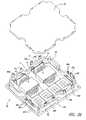
- FIG. 2Ashows a power module 50 according to one illustrated embodiment, the power module 50 housing a portion of the power converter 10 illustrated by broken line box 52 of FIG. 1 .
- the power module 50comprises an electrically insulative lead frame 54 , an integrated base plate heat sink 56 and an electrically insulative cover 58 , collectively forming a housing.
- the Figuredoes not separately call out the power semiconductor diodes D 6 -D 10 , which are formed as a part of the power semiconductor switches S 6 -S 10 in this illustrated embodiment.
- each of the power semiconductor switches S 7 -S 10 illustrated in FIG. 1may actually take the form of one or more (four illustrated) power semiconductor switches S 7 -S 10 electrically coupled in parallel with one another.
- the lead frame 54supports a number of external terminals or connectors making electrical couplings external from the housing formed by the lead frame 54 , heat sink 56 and cover 58 .
- the power module 50may include a number of terminals 60 a - 60 d for making electrical couplings between the phase nodes A, B, C of the inverter 12 and the poles of the first sides T 1 a , T 2 a of the transformers T 1 , T 2 .
- a first terminal 60 aelectrically couples the phase node A of the inverter 12 to the first pole T 1 c of the transformer T 1 , via wire bonds 61 .
- a second terminal 60 b and a third terminal 60 celectrically couple the phase node B of the inverter 12 to the second pole T 1 d of the first transformer T 1 and the first pole T 2 c of the second transformer T 2 , respectively, via wire bonds 61 .
- a fourth terminal 60 delectrically couples the phase node C of the inverter 12 to the second pole T 2 d of the second transformer T 2 via wire bonds 61 . While FIG. 2A only illustrates one wire bond 61 per electrical coupling, most practical applications with comprise a plurality of wire bonds for each electrical coupling.
- a number of terminals or connectorselectrically couple the rectifier 14 to the filter inductors L 1 -L 4 and to the terminals 18 a - 18 c via wire bonds (not shown).
- a pair of terminals 62 a , 62 belectrically couple the neutral node O of the rectifier 12 to the terminal 18 b .
- Other terminals 64 a - 64 delectrically couple the rectifier 14 and/or second sides T 1 b , T 2 b of the transformers T 1 , T 2 to the filter inductors L 1 -L 2 , via the current paths K-N.
- Terminals or connectorssuch as pins 66 a , 66 b , 66 c , 66 d electrically couple control signals 28 from the controller 24 to the power semiconductor switches S 7 -S 10 of the rectifier 14 via wire bonds (not shown).
- the pins 66 a - 66 dare located proximate the terminal 18 b which is connected to the neutral node O.
- the electrical couplings within the power module 50are advantageously made via wire bonds.
- the electrical couplings between the terminals 60 a - 60 d and the first side T 1 a , T 2 a of the transformers T 1 , T 2are made via wire bonds 61 .
- the electrical couplings between the second side T 1 b , T 2 b of the transformers T 1 , T 2 and the power semiconductor switches S 7 -S 10 and power semiconductor diodes D 7 -D 10are made via wire bonds (not shown).
- the electrical couplings between terminals 62 a , 62 b , 64 a - 64 b and the power semiconductor switches S 7 -S 10 and power semiconductor diodes D 7 -D 10are also made via wire bonds (not shown).
- FIGS. 2B-2Dshow how the power semiconductor switches S 7 -S 10 and power semiconductor diodes D 7 -D 10 of the rectifier 14 are physically mounted and thermally coupled to the integrated base plate heat sink 56 by one or more multi-layer switch substrates 44 , according to a number of illustrated embodiments.
- the multi-layer switch substrates 44comprise a first layer 44 a that is electrically and thermally conductive, a second layer 44 b that is electrically insulative and thermally conductive, and a third layer 44 c that is electrically and thermally conductive.
- the multi-layer switch substrate 44may comprise a greater number of layers.
- FIG. 2Bshows one embodiment in which a number of multi-layer switch substrates 44 are provided, one for each of the power semiconductor devices S 7 -S 10 and associated power semiconductor diodes D 7 -D 10 forming the rectifier 14 .
- this embodiment of FIG. 2Bmay include a total of four separate multi-layer switch substrates 44 for the rectifier 14 .
- FIG. 2Cshows another embodiment in which a number of multi-layer switch substrates 44 are provided, one for each leg 14 a , 14 b of the rectifier 14 .
- the electrically and thermally conductive layer 44 a of each of the multi-layer substrates 44form distinct areas for mounting each of the power semiconductor devices S 7 -S 10 and associated power semiconductor diodes D 7 -D 10 forming the respective leg 14 a , 14 b of the rectifier 14 .
- FIG. 2Dshows still a further embodiment in which a single multi-layer switch substrate 44 is provided for forming entire the rectifier 14 .
- a number of distinct areasare formed in the first electrically and thermally conductive layer 44 a , the areas being electrically isolated from one another.
- there is one area for each of the power semiconductor devices S 7 -S 10 and associated power semiconductor diodes D 7 -D 10 forming the rectifier 14thus a total of four distinct areas.
- the inclusion of fewer individual multi-layer substrates 44 , 70reduces the parts count, and may reduce the number of manufacturing operations, although forming distinct areas may offset some of the savings in manufacturing operations.
- a reduction in numberis typically accompanied by an increase in size of the remaining multi-layer substrate(s) 44 , 70 .
- This increase in sizeincreases the stresses to which the multi-layer substrates 44 , 70 are subject, and thus increases the likelihood of defects occurring, such as cracks developing, for example, from solder reflow.
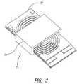
- FIGS. 3 and 4show one of the transformers T 1 in more detail.
- the second transformer T 2may have a similar construction to that of the first transformer T 1 .
- the transformer T 1comprises a multi-layer transformer substrate 70 and magnetic core 72 .
- the multi-layer transformer substrate 70includes a first layer 70 a that is electrically and thermally conductive, a second layer 70 b that is electrically insulative and thermally conductive, a third layer 70 c that is electrically and thermally conductive, a fourth layer 70 d that is electrically insulative and thermally conductive, and a fifth layer 70 f that is electrically and thermally conductive.
- the multi-layer transformer substrate 70may include a greater number of layers to vary the performance of the transformer T 1 , for example, by varying the number of layers and hence the ratio of “turns” between the primary and secondary windings of the transformer and/or by reducing eddy currents.
- the first layer 70 a and fifth layer 70 eare patterned to form portions of a first winding, and electrically coupled through vias 74 a , 74 b and connecting pads 74 c , 74 d , 74 e to form the first winding.
- the third layer 70 cis also patterned to form a second winding. While the Figures illustrate the first winding comprising more layers than the second winding, in some embodiments the second winding may comprises more layers than the first winding, or may the first and second windings may comprises the same number of layers.
- the fifth layer 70 emay be further patterned to form mounting areas 70 f for attaching the multi-layer transformer substrate 70 to the heat sink 56 , for example by soldering. This reduces the coupling area between the multi-layer substrate 70 and the integrated base plate heat sink 56 reducing associated stresses and the likelihood of imperfections developing such as cracking, for example, during solder reflow.
- the magnetic core 72may include two or more portions 72 a , 72 b that wrap around the first and second windings of the multi-layer transformer substrate 70 .
- a portion 72 c of the magnetic core 72may be received through an opening 70 g formed in each of the layers 70 a - 70 e of the multi-layer transformer substrate 70 .
- the multi-layer transformer substrate 70may be formed using a variety of techniques and materials, for example, the multi-layer substrates 70 may take the form of direct bonded copper (DBC) substrates available, for example, from Curamik Electronics of Addison, Tex. Additionally or alternatively, the multi-layer substrates 70 may take the form of insulated metal substrates (IMS) available, for example, from Bergquist Company of Chanhassen, Minn.
- DBCdirect bonded copper
- IMSinsulated metal substrates
- the electrically and thermally conductive layersmay take a variety of forms such as copper, aluminum and/or other good electrical and thermal conductors. While typically provided in the form of a film, the electrically and thermally conductive layers may take other forms, for example, stamped sheet metal.
- the electrically insulative and thermally conductive layersmay, for example, take the form of a thermally enhanced polyimide film such as Kapton® film, available from Du Pont de Nemours, High Performance Materials of Circleville, Ohio. Additionally, or alternatively, the electrically insulative and thermally conductive layers may, for example, take the from of a suitable ceramic, such as an alumina, aluminum nitride and/or silicon nitride ceramic.
- the multi-layer transformer substrate 70takes the form of layers of stamped sheet metal that are laminated together with insulative layers such as Mylar® film, available from Du Pont de Nemours, High Performance Materials of Circleville, Ohio, using an adhesive such as an epoxy based adhesive.
- the multi-layer switch and transformer substrates 44 , 70may be attached to the integrated base plate heat sink 56 via solder reflow techniques.
- the power semiconductor switches S 1 -S 10 and power semiconductor diodes D 1 -D 10may be soldered onto respective multi-layer substrates 44 , 70 , which are then positioned on the integrated base plate heat sink 56 .
- the multi-layer substrates 44 , 70are then soldered to the integrated base plate heat sink 56 at a same time and/or in a single act, for example, via heating in an oven using solder reflow techniques.
- the multi-layer substrates 44 , 70may be positioned on the integrated base plate heat sink 56
- the power semiconductor switches S 1 -S 10 and power semiconductor diodes D 1 -D 10may be positioned on the multi-layer substrates 44 , 70 .
- the connections between the power semiconductor switches S 1 -S 10 and power semiconductor diodes D 1 -D 10 and between the multi-layer substrates 44 , 70 and the integrated base plate heat sink 56may be made at a same time and/or in a single act, for example, via heating in an oven using solder reflow techniques.
- FIGS. 5 and 6show one of the inductors L 1 formed as a planar inductor, according to one illustrated embodiment.
- the other inductors L 2 -L 4may have a similar construction to that of the first planar inductor L 1 .
- the power converter 10may employ conventional inductors.
- the inductor L 1comprises a multi-layer inductor substrate 80 and magnetic core 82 .
- the multi-layer inductor substrate 80includes a first layer 80 a that is electrically and thermally conductive, a second layer 80 b that is electrically insulative and thermally conductive, a third layer 80 c that is electrically and thermally conductive, a fourth layer 80 d that is electrically insulative and thermally conductive, and a fifth layer 80 f that is electrically and thermally conductive.
- the multi-layer inductor substrate 80may include a greater number of layers to vary the performance of the planar inductor L 1 , for example, by varying the number of layers and hence the ratio of “turns” of the winding of the inductor and/or by reducing eddy currents.
- the first layer 80 a and third layer 80 care patterned to form portions of a first winding, and electrically coupled through vias 84 a , 84 b and connecting pads 84 c , 84 d to form the first winding.
- the magnetic core 82may include two or more portions 82 a , 82 b that wrap around the first winding of the multi-layer inductor substrate 80 .
- a portion 82 c of the magnetic core 82may be received through an opening 80 g formed in each of the layers 80 a - 80 e of the multi-layer inductor substrate 80 .
- the multi-layer inductor substrate 80may be formed using a variety of techniques and materials, for example, the multi-layer substrates 80 may take the form of direct bonded copper (DBC) substrates available, for example, from Curamik Electronics of Addison, Tex. Additionally or alternatively, the multi-layer substrates 70 may take the form of insulated metal substrates (IMS) available, for example, from Bergquist Company of Chanhassen, Minn.
- DBCdirect bonded copper
- IMSinsulated metal substrates
- the electrically and thermally conductive layersmay take a variety of forms such as copper, aluminum and/or other good electrical and thermal conductors. While typically provided in the form of a film, the electrically and thermally conductive layers may take other forms, for example, stamped sheet metal.
- the electrically insulative and thermally conductive layersmay, for example, take the form of a thermally enhanced polyimide film such as Kapton® film, available from Du Pont de Nemours, High Performance Materials of Circleville, Ohio. Additionally, or alternatively, the electrically insulative and thermally conductive layers may, for example, take the from of a suitable ceramic, such as an alumina, aluminum nitride and/or silicon nitride ceramic.
- the multi-layer inductor substrate 80takes the form of layers of stamped sheet metal that are laminated together with insulative layers such as Mylar® film, available from Du Pont de Nemours, High Performance Materials of Circleville, Ohio, using an adhesive such as an epoxy based adhesive.
- the multi-layer switch and inductor substrates 44 , 70may be attached to the integrated base plate heat sink 56 via solder reflow techniques.
- the power semiconductor switches S 1 -S 10 and power semiconductor diodes D 1 -D 10may be soldered onto respective multi-layer substrates 44 , 80 , which are then positioned on the integrated base plate heat sink 56 .
- the multi-layer substrates 44 , 80are then soldered to the integrated base plate heat sink 56 at a same time and/or in a single act, for example, via heating in an oven using solder reflow techniques.
- the multi-layer substrates 44 , 80may be positioned on the integrated base plate heat sink 56
- the power semiconductor switches S 1 -S 10 and power semiconductor diodes D 1 -D 10may be positioned on the multi-layer substrates 44 , 70 .
- the connections between the power semiconductor switches S 1 -S 10 and power semiconductor diodes D 1 -D 10 and between the multi-layer substrates 44 , 80 and the integrated base plate heat sink 56may be made at a same time and/or in a single act, for example, via heating in an oven using solder reflow techniques.
- the described techniquesmay reduce the number of acts involved in manufacturing the power module thereby reducing manufacturing costs, and also subject the various elements to less thermal cycles advantageously increasing reliability and throughput.
- FIG. 7Ashows the power module 50 according to another illustrated embodiment, housing the entire power converter 10 of FIG. 1 , other than the controller 24 .
- the power module 50 of FIG. 7Aincludes the inverter 12 , rectifier 14 and transformers T 1 , T 2 .
- a pair of terminals 20 a , 20 ballow electrical connections to be made to the power source VI.
- Three terminals 18 a , 18 b , 18 callow electrical connections to be made to the load(s) R 1 , R 2 .
- the terminals 18 a , 18 cmay be formed as bus bars 90 a , 90 b .
- Terminals or connectorssuch as pins 95 a - 95 f , receive control signals 26 from the controller 24 for operating the power semiconductor switches S 1 -S 6 of the inverter.
- the power semiconductor switches S 1 -S 6 and associated power semiconductor diodes D 1 -D 6 of the inverter 12may advantageously be electrically coupled to the first sides T 1 a , T 2 a of the transformers T 1 , T 2 via wire bonds 91 , only a few of which are illustrated.
- the first sides T 1 a , T 2 a of the transformers T 1 , T 2may advantageously be electrically coupled to the power semiconductor switches S 7 -S 10 and associated power semiconductor diodes D 7 -D 10 of the rectifier 14 via wire bonds 93 , only a few of which are illustrated.
- the power module 50may include one or more additional multi-layer switch substrates 44 for mounting the power semiconductor switches S 1 -S 10 and associated power semiconductor diodes D 1 -D 10 forming the inverter 12 to the integrated base plate heat sink 56 .
- the power module 50may comprise a separate multi-layer switch substrate 44 for each of the power semiconductor switches S 1 -S 6 and associated power semiconductor diodes D 1 -D 6 pairs of the inverter 12 , in fashion similar to that shown in FIG. 2B for the rectifier 14 .
- the power module 50may include six separate multi-layer switch substrates 44 for the inverter 12 .
- the power module 50may comprise a separate multi-layer switch substrate 44 for each phase leg 12 a - 12 c of the inverter 12 .
- the electrically conductive layer 44 a of each multi-layer switch substrate 44is formed into two distinct areas, one for each of the power semiconductor switches S 1 -S 6 and associated power semiconductor diodes D 1 -D 6 of the respective phase leg 12 a - 12 c , in a similar fashion to that of FIG. 2C for the rectifier 14 .
- the power module 50may include three additional multi-layer switch substrates 44 for the inverter 12 .
- the power module 50may comprise a single additional multi-layer switch substrate 44 for mounting all of the power semiconductor switches S 1 -S 6 and associated power semiconductor diodes D 1 -D 6 of the inverter 12 , in a similar fashion to that of FIG. 2D for the rectifier 14 .
- the multi-layer switch substrate 44may include six distinct areas formed in the electrically and thermally conductive layer 44 a , one area for each power semiconductor S 1 -S 6 and associated diode D 1 -D 6 pair.
- FIG. 7Bshows a single multi-layer switch substrate 44 for mounting the power semiconductor switches S 1 -S 6 and associated power semiconductor diodes D 1 -D 6 forming the inverter 12 , along with the power semiconductor devices S 7 -S 10 and associated power semiconductor diodes D 7 -D 10 forming the rectifier 14 .
- a further embodiment illustrated in FIG. 7Bmay include ten distinct areas formed in the first electrically and thermally conductive layer 44 a , the areas electrically isolated from one another.
- FIG. 7Cshows a single multi-layer switch substrate 70 comprising at least three electrically and thermally conductive layers 70 a , 70 c , 70 e and at least two electrically insulative and thermally conductive layers 70 b , 70 d separating respective pairs of the electrically and thermally conductive layers 70 a - 70 c , 70 c - 70 e .
- the second electrically and thermally conductive layer 70 c of the multi-layer switch substrate 70form ten distinct areas. The areas are electrically isolated from one another, for mounting the power semiconductor switches S 1 -S 6 and associated power semiconductor diodes D 1 -D 6 (not shown in FIG.
- At least the first and third electrically and thermally conductive layers 70 a , 70 eare patterned and electrically coupled to one another to form a first winding of a transformer T 1 , T 2 .
- At least the second electrically and thermally conductive layer 70 cis patterned to form a second winding of the transformer T 1 , T 2 .
- FIG. 7Cillustrates three electrically and thermally conductive layers 70 a , 70 c , 70 e and two electrically insulative and thermally conductive layers 70 b , 70 d
- the multi-layer substrate 70may include a greater number of layers.
- the power semiconductor devices S 1 -S 10 , D 1 -D 10are illustrated as mounted to the second electrically and thermally conductive layer, some or all of those power semiconductor devices may be mounted on other ones of the electrically and thermally conductive layers.
- FIG. 7Dshows a portion of an integrated base plate heat sink similar to that of FIG. 7C , illustrating the use of one of the second electrically and thermally conductive layer 70 c of the multi-layer substrate 70 to electrically couple the second sides T 1 b , T 2 b of the transformers T 1 , T 2 to respective terminals (e.g., drain/collector) of the power semiconductor switches S 7 -S 10 and/or power semiconductor diodes D 7 -D 10 of the rectifier 14 , advantageously eliminating a number of the wire bonds.
- Other embodimentsmay employ the same or other electrically and thermally conductive layers 70 a , 70 c , 70 e , in a similar manner, for example, to eliminate wire bonds.
- FIG. 7Eshows a portion of an integrated base plate heat sink similar to that of FIG. 7D , illustrating the use of one of the second electrically and thermally conductive layer 70 c of the multi-layer substrate 70 to electrically couple the second sides T 1 b , T 2 b of the transformers T 1 , T 2 to respective terminals (e.g., drain/collector) of the power semiconductor switches S 7 -S 10 and/or power semiconductor diodes D 7 -D 10 of the rectifier 14 , and to planar inductors L 1 -L 4 , advantageously eliminating a number of the wire bonds.
- Other embodimentsmay employ the same or other electrically and thermally conductive layers 70 a , 70 c , 70 e , in a similar manner, for example, to eliminate wire bonds.
- FIG. 8shows the integrated base plate heat sink 56 according to one embodiment.
- the integrated base plate heat sink 56may comprise a plate section 56 a and conduit section 56 b .
- the plate section 56 aincludes a top surface 92 having a pair of recesses 92 a , 92 b sized and dimensioned to receive a portion of the magnetic core 72 such as the portion 72 b such that the multi-layer transformer substrate 70 is flush with the surface 92 .
- the conduit section 56 bcomprises an inlet 94 a , an outlet 94 b and a passage formed by first passage section 96 a and second passage section 96 b which are fluidly communicatingly coupled with the intake 94 a and outtake 94 b .
- the plate 92may include thermal radiating structures such as fins or pins 97 on a surface opposed to the top surface 92 which are received in the portions 96 a , 96 b for transferring heat from the plate 56 a to a fluid passing through the conduit portions 96 a , 96 b .
- the power converter 10may include a circulation system (not shown) including, for example, a pump, compressor, and/or fan for circulating fluid through the conduit portions 96 a , 96 b to assist in transferring heat from the integrated base plate heat sink 56 . While shown as an integrated base plate heat sink 56 , other embodiment may employ other forms of heat sinks.
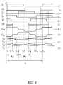
- FIG. 9shows a timing diagram illustrating switching signals applied to the semiconductor switches S 1 -S 6 of the inverter 12 , the voltage U AB applied to the first side T 1 a of the transformer T 1 and the voltage U BC applied to the first side T 2 a of the second transformer T 2 at various time intervals t 0 -t 12 over a period T S .
- FIG. 9also shows the current output I L1 -I L4 of the filter inductors L 1 -L 4 , respectively.
- the power semiconductor switches S 1 -S 6 ( FIG. 1 ) of each phase leg 12 a - 12 c of the inverter 12each generate a nearly 50% duty cycle square waveform.
- the first and second phase legs 12 a , 12 b of the inverter 12are phase shift controlled to generate a three-level square waveform U AB applied to the first side or winding T 1 a of the first transformer T 1 .
- the second leg 12 b and third leg 12 c of the inverter 12are phase shifted controlled to generate a three-level square wave form U BC to the first side or winding T 2 a of the second transformer T 2 .
- phase Bis shared by the transformers T 1 , T 2 to form the equivalent of two conventional full bridge DC/DC converters, while advantageously saving one high voltage leg (i.e., at least two power semiconductor switches and associated power semiconductor diodes) and gate driver circuit.
- the two outputs U AB and U BCare phase locked to each other, so that the second phase leg 12 b (phase B) can achieve a wide soft-switching range by means of the load current in the transformers T 1 .
- the soft switchingis achieve by the energy stored in the filter inductors L 1 -L 4 , without relying on the energy stored in the leakage inductance of the transformers T 1 .
- the output voltage Vout 1is regulated by a phase shift angle ⁇ AB
- the output voltage Vout 2is regulated by a phase shift angle ⁇ BC.
- the power converter 10can be configured as either single output or dual output.
- single output configurationthe outputs Vout 1 and Vout 2 are paralleled together to double the output current/power. If Vout 1 and Vout 2 are paralleled together in a single output voltage configuration, the phase shift angles ⁇ AB , ⁇ BC are equal.
- dual output configurationVout 1 and Vout 2 may be controlled independently.
- the interleaved full bridge DC/DC power converter 10 described abovedoubles output power capability while operating at a high coolant temperature (e.g., 105° C.) and maintaining current and thermal stress at acceptable levels to provide high reliability. Soft switching is achieved over a wide range of loads, reducing switching losses and providing high efficiency operation by means of the load currents in the transformers T 1 , T 2 and filter inductors L 1 -L 4 .
- the described power convertermay efficiently provide high power conversion, with high power density and high coolant temperature.
- the interleavingalso advantageously reduces high frequency ripple current to the input and output capacitors CI, CO 1 , CO 1 .
- Sharing of a phase leg 12 a - 12 c of the inverter 12allows the use of one less inverter phase leg (i.e., at least two power semiconductor switches and associated diodes) than would typically be required, reducing parts count, complexity, and cost while increasing reliability.
- the power converter 10is further easily configurable as either a single or dual output unit.
- planar transformers and/or planar inductors in the power converter 10 described aboveavoids or reduces the use of conventional air-cooled heavy copper printed circuit board windings and traditional wound wire inductors.
- the integration of planar transformers and/or planar inductorsmay allow a reduction in Ohmic losses and inductance related to contacts, which are particularly problematic at high frequencies, by employing direct wire bonding connections as described above. Leakage inductance and AC loss may be reduced by employing the flat winding structure of the planar transformers T 1 , T 2 and/or the planar inductors L 1 , L 2 , L 3 , and L 4 .
- planar transformers and/or planar inductors in the described power converter 10may advantageously allow an increase in the magnetic core window utilization ratio, a reduction in the magnetic core value, and an increase in power density.
- the power converter 10 described abovemay also provide enhanced EMI performance.
- the power converter 10may share the first or third phase legs 12 a , 12 c , rather than the second phase leg 12 b .
- the teachingsare not limited to a three phase inverter 12 , but may be applied to inverters with an even greater number of phase legs, for example, to provide even high power.
- the power converter 10may comprise a fourth phase leg added to the inverter 12 , and a third transformer electrically coupled between the third phase leg 12 c and the added phase leg.
- the power convertermay also comprise two filter inductors, along with adding power semiconductor switches and associated diodes to the rectifier which are supplied from the second side of the third transformer to provide a power increase of 50%.
- synchronized rectificationis optional, and may be omitted in some embodiments, for example being replaced by a diode rectifier.
- the integrated planar transforms or planar inductorsmay be advantageously employed in other power converters such as inverters and/or rectifiers.
- the interleavingmay be advantageously employed without the integrated planar transformers or planar inductors.
Landscapes
- Engineering & Computer Science (AREA)
- Power Engineering (AREA)
- Physics & Mathematics (AREA)
- Thermal Sciences (AREA)
- Microelectronics & Electronic Packaging (AREA)
- Dc-Dc Converters (AREA)
- Coils Or Transformers For Communication (AREA)
- Rectifiers (AREA)
Abstract
Description
Claims (50)
Priority Applications (6)
| Application Number | Priority Date | Filing Date | Title |
|---|---|---|---|
| US10/964,000US7289329B2 (en) | 2004-06-04 | 2004-10-12 | Integration of planar transformer and/or planar inductor with power switches in power converter |
| EP05756368.6AEP1756935B1 (en) | 2004-06-04 | 2005-05-27 | Integration of planar transformer and/or planar inductor with power switches in power converter |
| PCT/US2005/018794WO2005122377A1 (en) | 2004-06-04 | 2005-05-27 | Integration of planar transformer and/or planar inductor with power switches in power converter |
| JP2007515402AJP4705636B2 (en) | 2004-06-04 | 2005-05-27 | Integration of planar transformer and / or planar inductor and power switch in power converter |
| KR1020077000256AKR20070050907A (en) | 2004-06-04 | 2005-05-27 | Integration of Power Switches and Planar Transformers and / or Planar Inductors in Power Converters |
| CA002567523ACA2567523A1 (en) | 2004-06-04 | 2005-05-27 | Integration of planar transformer and/or planar inductor with power switches in power converter |
Applications Claiming Priority (2)
| Application Number | Priority Date | Filing Date | Title |
|---|---|---|---|
| US56075504P | 2004-06-04 | 2004-06-04 | |
| US10/964,000US7289329B2 (en) | 2004-06-04 | 2004-10-12 | Integration of planar transformer and/or planar inductor with power switches in power converter |
Publications (2)
| Publication Number | Publication Date |
|---|---|
| US20050270745A1 US20050270745A1 (en) | 2005-12-08 |
| US7289329B2true US7289329B2 (en) | 2007-10-30 |
Family
ID=34971721
Family Applications (1)
| Application Number | Title | Priority Date | Filing Date |
|---|---|---|---|
| US10/964,000Expired - LifetimeUS7289329B2 (en) | 2004-06-04 | 2004-10-12 | Integration of planar transformer and/or planar inductor with power switches in power converter |
Country Status (6)
| Country | Link |
|---|---|
| US (1) | US7289329B2 (en) |
| EP (1) | EP1756935B1 (en) |
| JP (1) | JP4705636B2 (en) |
| KR (1) | KR20070050907A (en) |
| CA (1) | CA2567523A1 (en) |
| WO (1) | WO2005122377A1 (en) |
Cited By (69)
| Publication number | Priority date | Publication date | Assignee | Title |
|---|---|---|---|---|
| US20050126811A1 (en)* | 2003-11-14 | 2005-06-16 | Masayuki Hirota | Filter apparatus and frequency converter to which the filter apparatus is connected |
| US20070253164A1 (en)* | 2006-04-27 | 2007-11-01 | Takeshi Matsuo | Power inverter |
| US20080101032A1 (en)* | 2006-10-26 | 2008-05-01 | Roman Tschirbs | Base Plate For A Power Semiconductor Module |
| US20080136363A1 (en)* | 2004-12-03 | 2008-06-12 | Continental Automotive Systems Us, Inc. | Method, apparatus and article for load stabilization |
| US20080174393A1 (en)* | 2007-01-22 | 2008-07-24 | Johnson Controls Technology Company | Cooling systems for variable speed drives and inductors |
| US20080174116A1 (en)* | 2007-01-19 | 2008-07-24 | Nico Peterschmidt | Feed converter system |
| US20090079528A1 (en)* | 2007-09-25 | 2009-03-26 | Flextronics Ap, Llc | Thermally enhanced magnetic transformer |
| US20090153284A1 (en)* | 2007-12-17 | 2009-06-18 | Gm Global Technology Operations, Inc. | Inductor packaging for power converters |
| US20090241575A1 (en)* | 2008-03-28 | 2009-10-01 | Johnson Controls Technology Company | Cooling member |
| US20100014252A1 (en)* | 2007-03-19 | 2010-01-21 | Toyota Jidosha Kabushiki Kaisha | Electric unit having capacitor |
| US20100071396A1 (en)* | 2007-01-22 | 2010-03-25 | Johnson Controls Technology Company | Cooling member |
| US20100148909A1 (en)* | 2008-12-15 | 2010-06-17 | General Electric Company | High energy density inductor |
| US20100237976A1 (en)* | 2009-03-17 | 2010-09-23 | Li Chiu K | Low-profile inductive coil and methond of manufacture |
| US20110242860A1 (en)* | 2010-04-06 | 2011-10-06 | Fuji Electric Holdings Co., Ltd. | Power semiconductor device and power conversion system using the device |
| US20110292617A1 (en)* | 2010-05-25 | 2011-12-01 | Lear Corporation | Power module with current sensing |
| WO2012034190A1 (en)* | 2010-09-17 | 2012-03-22 | Intervention Technology Pty Ltd | A power supply device and components thereof |
| US8339231B1 (en) | 2010-03-22 | 2012-12-25 | Flextronics Ap, Llc | Leadframe based magnetics package |
| US8339808B2 (en) | 2009-06-19 | 2012-12-25 | Tdk Corporation | Switching power supply unit |
| US8376069B2 (en)* | 2008-07-29 | 2013-02-19 | Hitachi, Ltd. | Power conversion apparatus and electric vehicle |
| US20130155633A1 (en)* | 2011-12-14 | 2013-06-20 | Timotion Technology Co., Ltd | Power supply module of linear actuator and conversion assembly thereof |
| US20130312930A1 (en)* | 2012-05-22 | 2013-11-28 | Lear Corporation | Coldplate for use with a Transformer in an Electric Vehicle (EV) or a Hybrid-Electric Vehicle (HEV) |
| US20140016289A1 (en)* | 2012-07-06 | 2014-01-16 | Cyntec Co., Ltd | Network communication device |
| US20140120774A1 (en)* | 2012-11-01 | 2014-05-01 | Samsung Electronics Co., Ltd. | Substrate for power module having uniform parallel switching characteristic and power module including the same |
| US8736133B1 (en) | 2013-03-14 | 2014-05-27 | Boulder Wind Power, Inc. | Methods and apparatus for overlapping windings |
| US20140226283A1 (en)* | 2013-02-13 | 2014-08-14 | Gerald Ho Kim | Isolation Of Thermal Ground For Multiple Heat-Generating Devices On A Substrate |
| US8823241B2 (en) | 2009-01-16 | 2014-09-02 | Boulder Wind Power, Inc. | Segmented stator for an axial field device |
| US8878483B2 (en) | 2011-01-14 | 2014-11-04 | Lear Corporation | Electronics unit with current sensing |
| US8971041B2 (en) | 2012-03-29 | 2015-03-03 | Lear Corporation | Coldplate for use with an inverter in an electric vehicle (EV) or a hybrid-electric vehicle (HEV) |
| US8971038B2 (en) | 2012-05-22 | 2015-03-03 | Lear Corporation | Coldplate for use in an electric vehicle (EV) or a hybrid-electric vehicle (HEV) |
| US8975523B2 (en) | 2008-05-28 | 2015-03-10 | Flextronics Ap, Llc | Optimized litz wire |
| US9030822B2 (en) | 2011-08-15 | 2015-05-12 | Lear Corporation | Power module cooling system |
| US9076593B2 (en) | 2011-12-29 | 2015-07-07 | Lear Corporation | Heat conductor for use with an inverter in an electric vehicle (EV) or a hybrid-electric vehicle (HEV) |
| US9130476B2 (en) | 2010-04-06 | 2015-09-08 | Fuji Electric Co., Ltd. | Power semiconductor device and power conversion system using the device |
| US9154024B2 (en) | 2010-06-02 | 2015-10-06 | Boulder Wind Power, Inc. | Systems and methods for improved direct drive generators |
| US20160029478A1 (en)* | 2014-07-28 | 2016-01-28 | Infineon Technologies Ag | Power Semiconductor Module System Having a High Isolation Strength and Method for Producing a Power Semiconductor Module Arrangement Having a High Isolation Strength |
| US9362040B2 (en) | 2014-05-15 | 2016-06-07 | Lear Corporation | Coldplate with integrated electrical components for cooling thereof |
| AU2011301708B2 (en)* | 2011-09-16 | 2017-03-02 | Intervention Technology Pty Ltd | A power supply device and components thereof |
| US9615490B2 (en) | 2014-05-15 | 2017-04-04 | Lear Corporation | Coldplate with integrated DC link capacitor for cooling thereof |
| US9620278B2 (en) | 2014-02-19 | 2017-04-11 | General Electric Company | System and method for reducing partial discharge in high voltage planar transformers |
| US9799720B2 (en) | 2014-09-12 | 2017-10-24 | International Business Machines Corporation | Inductor heat dissipation in an integrated circuit |
| US20170317604A1 (en)* | 2016-04-27 | 2017-11-02 | General Electric Company | Integrated power converter and transformer |
| US20180122562A1 (en)* | 2016-10-28 | 2018-05-03 | Delta Electronics, Inc. | Power module and magnetic component thereof |
| US20180166208A1 (en)* | 2016-05-31 | 2018-06-14 | Shindengen Electric Manufacturing Co., Ltd. | Coil structure and magnetic component |
| US20180226182A1 (en)* | 2017-02-03 | 2018-08-09 | Virginia Tech Intellectual Properties, Inc. | Matrix Transformer and Winding Structure |
| US10062496B2 (en) | 2015-02-26 | 2018-08-28 | Lear Corporation | Planar transformer |
| WO2018156934A1 (en)* | 2017-02-23 | 2018-08-30 | General Electric Company | Energy converting device, and device for energizing oil exploration device |
| US10147531B2 (en) | 2015-02-26 | 2018-12-04 | Lear Corporation | Cooling method for planar electrical power transformer |
| US10177620B2 (en) | 2014-05-05 | 2019-01-08 | Boulder Wind Power, Inc. | Methods and apparatus for segmenting a machine |
| US10186949B1 (en) | 2017-11-09 | 2019-01-22 | International Business Machines Corporation | Coupled-inductor DC-DC power converter |
| US10256737B2 (en) | 2016-08-08 | 2019-04-09 | Hyundai Motor Company | Integrated magnetic apparatus and DC-DC converter including the same |
| US10321585B2 (en) | 2008-07-29 | 2019-06-11 | Hitachi, Ltd. | Power conversion apparatus and electric vehicle |
| US10355608B2 (en) | 2017-09-19 | 2019-07-16 | Chicony Power Technology Co., Ltd. | Power converter module |
| US10410784B2 (en)* | 2016-05-31 | 2019-09-10 | Shindengen Electric Manufacturing Co., Ltd. | Magnetic component |
| US10438736B2 (en) | 2016-10-28 | 2019-10-08 | Delta Electronics (Shanghai) Co., Ltd. | Magnetic component and manufacturing method thereof |
| US10643782B2 (en) | 2016-10-28 | 2020-05-05 | Delta Electronics (Shanghai) Co., Ltd. | Magnetic component and power module |
| US10840005B2 (en) | 2013-01-25 | 2020-11-17 | Vishay Dale Electronics, Llc | Low profile high current composite transformer |
| US10854367B2 (en) | 2016-08-31 | 2020-12-01 | Vishay Dale Electronics, Llc | Inductor having high current coil with low direct current resistance |
| US10939543B2 (en) | 2017-12-29 | 2021-03-02 | International Business Machines Corporation | Unified conductor to lower the resistance between a planar transformer and one or more inductors |
| US10998124B2 (en) | 2016-05-06 | 2021-05-04 | Vishay Dale Electronics, Llc | Nested flat wound coils forming windings for transformers and inductors |
| US11160167B2 (en)* | 2019-06-04 | 2021-10-26 | Delta Electronics, Inc. | Voltage regulator module and voltage regulation device with same |
| US20220084740A1 (en)* | 2020-09-14 | 2022-03-17 | Intel Corporation | Embedded cooling channel in magnetics |
| US20220199491A1 (en)* | 2020-12-21 | 2022-06-23 | Hyundai Motor Company | Motor drive device |
| US11387039B2 (en) | 2019-02-13 | 2022-07-12 | Astronics Advanced Electronic Systems Corp. | Integrated transformer with low AC losses and impedance balanced interface |
| US20220286040A1 (en)* | 2019-08-16 | 2022-09-08 | Wolfgang BAECK | Power electronic converter |
| US11665813B2 (en) | 2020-08-14 | 2023-05-30 | Toyota Motor Engineering & Manufacturing North America, Inc. | Power electronics cooling assemblies and methods for making the same |
| US11948724B2 (en) | 2021-06-18 | 2024-04-02 | Vishay Dale Electronics, Llc | Method for making a multi-thickness electro-magnetic device |
| USD1034462S1 (en) | 2021-03-01 | 2024-07-09 | Vishay Dale Electronics, Llc | Inductor package |
| US12156387B2 (en) | 2021-04-15 | 2024-11-26 | Carrier Corporation | Packaging of power conversion unit |
| WO2025023332A1 (en) | 2023-07-25 | 2025-01-30 | Mitsubishi Electric R&D Centre Europe Bv | Method and system for manufacturing printed circuit board with embedded cooling cavity, and printed circuit board |
Families Citing this family (96)
| Publication number | Priority date | Publication date | Assignee | Title |
|---|---|---|---|---|
| DE102005008521A1 (en)* | 2005-02-24 | 2006-08-31 | OCé PRINTING SYSTEMS GMBH | Arrangement and method for cooling a power semiconductor |
| EP2306634A3 (en) | 2005-06-30 | 2015-04-29 | Continental Automotive Systems US, Inc. | Control system for electric drives |
| US7456602B2 (en)* | 2005-11-18 | 2008-11-25 | Continental Automotive Systems Us, Inc. | System and method of commonly controlling power converters |
| JP4848187B2 (en)* | 2006-01-17 | 2011-12-28 | 日立オートモティブシステムズ株式会社 | Power converter |
| US7989981B2 (en) | 2006-02-02 | 2011-08-02 | Flextronics Ap, Llc | Power adaptor and storage unit for portable devices |
| JP4839096B2 (en)* | 2006-02-13 | 2011-12-14 | 株式会社日立産機システム | Power converter |
| JP4850564B2 (en) | 2006-04-06 | 2012-01-11 | 日立オートモティブシステムズ株式会社 | Power converter |
| US7826873B2 (en) | 2006-06-08 | 2010-11-02 | Flextronics Ap, Llc | Contactless energy transmission converter |
| US7636242B2 (en)* | 2006-06-29 | 2009-12-22 | Intel Corporation | Integrated inductor |
| US20080107933A1 (en)* | 2006-11-02 | 2008-05-08 | Gallagher Emerson R | Fuel cell hibernation mode method and apparatus |
| US7800921B2 (en)* | 2007-01-08 | 2010-09-21 | Continental Automotive Systems Us, Inc. | DC/DC converter |
| JP4436843B2 (en) | 2007-02-07 | 2010-03-24 | 株式会社日立製作所 | Power converter |
| JP4859700B2 (en)* | 2007-02-20 | 2012-01-25 | セイコーエプソン株式会社 | Coil unit and electronic equipment |
| US8994336B2 (en)* | 2007-02-26 | 2015-03-31 | Black & Decker Inc. | Portable alternating current inverter having reduced impedance losses |
| EP2866327B1 (en)* | 2007-02-26 | 2020-07-15 | Black & Decker Inc. | Portable power supply |
| US8191241B2 (en) | 2007-03-29 | 2012-06-05 | Flextronics Ap, Llc | Method of producing a multi-turn coil from folded flexible circuitry |
| US8400775B2 (en)* | 2007-07-06 | 2013-03-19 | GM Global Technology Operations LLC | Capacitor with direct DC connection to substrate |
| US7978489B1 (en) | 2007-08-03 | 2011-07-12 | Flextronics Ap, Llc | Integrated power converters |
| US7508289B1 (en)* | 2008-01-11 | 2009-03-24 | Ise Corporation | Cooled high power vehicle inductor and method |
| JP4819071B2 (en)* | 2008-02-06 | 2011-11-16 | 本田技研工業株式会社 | Electric vehicle and cooling method for DC / DC converter for vehicle |
| US9001527B2 (en)* | 2008-02-18 | 2015-04-07 | Cyntec Co., Ltd. | Electronic package structure |
| EP2284847B1 (en)* | 2008-04-24 | 2019-06-05 | Panasonic Intellectual Property Management Co., Ltd. | Transformer, power converter using the transformer, lighting device, lamp for vehicle, and vehicle |
| US8531174B2 (en) | 2008-06-12 | 2013-09-10 | Flextronics Ap, Llc | AC-DC input adapter |
| JP5332374B2 (en)* | 2008-07-25 | 2013-11-06 | サンケン電気株式会社 | Semiconductor device |
| JP4708487B2 (en)* | 2009-07-06 | 2011-06-22 | トヨタ自動車株式会社 | Inverter relay connection member |
| JP2011061924A (en)* | 2009-09-08 | 2011-03-24 | Tokai Rika Co Ltd | Inverter device |
| CN102763178B (en)* | 2010-02-19 | 2014-12-31 | 村田电源 | High current inductor assembly |
| JP5785365B2 (en)* | 2010-02-26 | 2015-09-30 | 株式会社ケーヒン | Switching power supply |
| JP5785363B2 (en)* | 2010-02-26 | 2015-09-30 | 株式会社ケーヒン | Transformer and switching power supply |
| CN101814837A (en)* | 2010-04-23 | 2010-08-25 | 威海金丰电子有限公司 | PCB (Printed Circuit Board) type switch power supply of ultrathin magnetic core |
| KR100978503B1 (en)* | 2010-04-23 | 2010-08-31 | 주식회사 시스하이텍 | Slim type high voltage transformer |
| KR101039276B1 (en)* | 2010-04-23 | 2011-06-07 | 주식회사 시스하이텍 | Slim high voltage transformer |
| WO2011156768A2 (en) | 2010-06-11 | 2011-12-15 | Mojo Mobility, Inc. | System for wireless power transfer that supports interoperability, and multi-pole magnets for use therewith |
| JP5563383B2 (en)* | 2010-06-21 | 2014-07-30 | 日立オートモティブシステムズ株式会社 | Power converter |
| JP5417314B2 (en)* | 2010-12-27 | 2014-02-12 | 日立オートモティブシステムズ株式会社 | Power converter |
| JP5641230B2 (en) | 2011-01-28 | 2014-12-17 | 株式会社豊田自動織機 | Electronics |
| FI125567B (en)* | 2011-02-28 | 2015-11-30 | Convion Oy | Method and arrangement for improved operation of a high temperature fuel cell system |
| CN103703616B (en)* | 2011-07-22 | 2018-12-07 | 日立金属株式会社 | antenna |
| JP5693419B2 (en) | 2011-08-31 | 2015-04-01 | 三菱電機株式会社 | Electrical equipment housing |
| CN103066859A (en)* | 2011-10-19 | 2013-04-24 | 台达电子企业管理(上海)有限公司 | High-power high-voltage frequency inverter power unit |
| JP5743851B2 (en)* | 2011-10-31 | 2015-07-01 | 日立オートモティブシステムズ株式会社 | Electronic equipment |
| US8824161B2 (en)* | 2012-06-15 | 2014-09-02 | Medtronic, Inc. | Integrated circuit packaging for implantable medical devices |
| KR20140006392A (en)* | 2012-07-05 | 2014-01-16 | 엘에스산전 주식회사 | Electronic component box for vehicle |
| KR101452076B1 (en)* | 2012-12-28 | 2014-10-16 | 삼성전기주식회사 | Coil for cordless charging and cordless charging apparatus using the same |
| US9853562B2 (en)* | 2013-02-28 | 2017-12-26 | Siemens Aktiengesellschaft | Converter station with diode rectifier |
| JP2014175631A (en)* | 2013-03-13 | 2014-09-22 | Omron Automotive Electronics Co Ltd | Magnetic device |
| JP6213979B2 (en)* | 2013-03-14 | 2017-10-18 | オムロンオートモーティブエレクトロニクス株式会社 | Magnetic device |
| JP6120619B2 (en)* | 2013-03-14 | 2017-04-26 | オムロンオートモーティブエレクトロニクス株式会社 | Magnetic device |
| JP6084079B2 (en)* | 2013-03-15 | 2017-02-22 | オムロンオートモーティブエレクトロニクス株式会社 | Magnetic device |
| JP6084147B2 (en)* | 2013-03-15 | 2017-02-22 | オムロンオートモーティブエレクトロニクス株式会社 | Coil integrated printed circuit board, magnetic device |
| JP6084148B2 (en)* | 2013-03-15 | 2017-02-22 | オムロンオートモーティブエレクトロニクス株式会社 | Coil integrated printed circuit board, magnetic device |
| KR200474884Y1 (en) | 2013-03-20 | 2014-10-22 | 엘에스산전 주식회사 | Power converter for electric vehicle |
| KR101463784B1 (en)* | 2013-07-19 | 2014-11-21 | 주식회사 이지트로닉스 | Inverter for Range-Extended Electric Vehicle |
| US10243248B2 (en)* | 2013-12-31 | 2019-03-26 | Skyworks Solutions, Inc. | Devices and methods related to high power diode switches |
| JP6429889B2 (en)* | 2014-09-25 | 2018-11-28 | 日立オートモティブシステムズ株式会社 | Power converter |
| KR102286337B1 (en)* | 2014-10-17 | 2021-08-04 | 쓰리엠 이노베이티브 프로퍼티즈 컴파니 | Emi shielding structure and thermal pad, and electronic circuit board assembly including the same |
| US20160261179A1 (en)* | 2015-03-02 | 2016-09-08 | Ati Technologies Ulc | Methods and apparatus including integrated conducting and inductive element for providing current |
| US9935677B2 (en) | 2015-06-30 | 2018-04-03 | Skyworks Solutions, Inc. | Devices and methods related to high power diode switches with low DC power consumption |
| US20170062385A1 (en)* | 2015-08-28 | 2017-03-02 | Electronics And Telecommunications Research Institute | Power converting device |
| EP3145286B1 (en)* | 2015-09-15 | 2019-05-01 | ABB Schweiz AG | Heat dissipation in power electronic assemblies |
| KR101821878B1 (en)* | 2016-02-24 | 2018-01-24 | 엘에스산전 주식회사 | Inverter |
| CN107171532B (en)* | 2016-03-03 | 2019-02-12 | 台达电子企业管理(上海)有限公司 | Power module |
| DE102016203613A1 (en)* | 2016-03-04 | 2017-09-07 | Würth Elektronik GmbH & Co. KG | Electronic component and method for its production |
| FR3053182B1 (en)* | 2016-06-22 | 2018-07-27 | IFP Energies Nouvelles | SYSTEM AND METHOD FOR CONVERTING A CONTINUOUS ELECTRICAL POWER TO A THREE-PHASE ALTERNATIVE ELECTRICAL POWER WITH AIR RADIATOR |
| WO2018006960A1 (en)* | 2016-07-07 | 2018-01-11 | Huawei Technologies Co., Ltd. | Two-transformer three-phase dc-dc resonant converter |
| JP6696343B2 (en)* | 2016-07-29 | 2020-05-20 | Tdk株式会社 | Coil device |
| US10395819B2 (en)* | 2016-08-30 | 2019-08-27 | Astec International Limited | Multiple phase power converters having integrated magnetic cores for transformer and inductor windings |
| JP6520875B2 (en)* | 2016-09-12 | 2019-05-29 | 株式会社村田製作所 | Inductor component and inductor component built-in substrate |
| KR20180056200A (en)* | 2016-11-18 | 2018-05-28 | 주식회사 이지트로닉스 | Integrated generating module for engine generating electric vehicle |
| JP6844253B2 (en)* | 2016-12-27 | 2021-03-17 | 富士電機株式会社 | Power supply, primary block and secondary block |
| KR102486164B1 (en)* | 2017-12-18 | 2023-01-10 | 현대자동차주식회사 | Cooling structure for planar transformer |
| JP6988432B2 (en)* | 2017-12-18 | 2022-01-05 | 株式会社デンソー | Reactor unit |
| KR20190134058A (en)* | 2018-05-24 | 2019-12-04 | 엘지전자 주식회사 | Core, transformer, power converting apparatus, and photovoltaic module including the same |
| FR3087614B1 (en)* | 2018-10-19 | 2020-10-09 | Sagemcom Energy & Telecom Sas | ELECTRICAL BOARD INCLUDING A RECOVERY BRIDGE |
| CN109686538B (en)* | 2018-12-11 | 2020-07-28 | 华为技术有限公司 | A transformer and power supply |
| EP3675144B1 (en)* | 2018-12-24 | 2021-10-20 | Wang, Wen-Chin | Manufacturing method of transformer circuit board and transformer thereof |
| US11482477B2 (en)* | 2018-12-31 | 2022-10-25 | Texas Instruments Incorporated | Packaged electronic device with suspended magnetic subassembly |
| JP7162545B2 (en)* | 2019-01-30 | 2022-10-28 | 三菱電機株式会社 | car charger |
| US20220093321A1 (en)* | 2019-02-22 | 2022-03-24 | Mitsubishi Electric Corporation | Power converter and coil apparatus |
| US11749433B2 (en) | 2019-03-05 | 2023-09-05 | Astec International Limited | Transformers having integrated magnetic structures for power converters |
| DE112020001754T5 (en)* | 2019-04-05 | 2021-12-16 | Mitsubishi Electric Corporation | Power conversion device |
| DE102019003373B4 (en)* | 2019-05-14 | 2023-08-10 | Infineon Technologies Austria Ag | Power semiconductor device with integrated current measurement and power module comprising this and method for measuring a current therein |
| US11056413B2 (en) | 2019-05-21 | 2021-07-06 | International Business Machines Corporation | Combined inductor and heat transfer device |
| CN113853737B (en)* | 2019-05-27 | 2025-07-15 | 三菱电机株式会社 | Power conversion device and method for manufacturing the same |
| US11271490B1 (en)* | 2019-07-29 | 2022-03-08 | Vicor Corporation | Multi-cell power converter |
| US11870340B1 (en)* | 2019-07-29 | 2024-01-09 | Vicor Corporation | Multi-cell power converter |
| WO2021092106A1 (en)* | 2019-11-07 | 2021-05-14 | Hyperloop Technologies, Inc. | A force-producing electromagnetic machine |
| KR20210089964A (en)* | 2020-01-09 | 2021-07-19 | 엘지이노텍 주식회사 | Substrate module for transformer and power module |
| EP3905859B1 (en)* | 2020-04-01 | 2023-08-30 | Hamilton Sundstrand Corporation | Thermal management of planar transformer windings and cores |
| KR102796662B1 (en)* | 2020-04-06 | 2025-04-16 | 삼성전자주식회사 | Transformer device and electronic apparatus including this |
| CN111785478B (en)* | 2020-07-10 | 2024-12-20 | 张家港鑫峰机电有限公司 | A low-loss planar inductor |
| KR102829554B1 (en)* | 2020-07-13 | 2025-07-04 | 현대자동차주식회사 | Converter using planar transformer |
| CN113891544B (en)* | 2021-08-26 | 2024-04-12 | 华为技术有限公司 | Magnetic power device and power module using same |
| US20230361049A1 (en)* | 2022-05-06 | 2023-11-09 | Ge Aviation Systems Llc | Modular power overlay device and method |
| DE102022205493A1 (en)* | 2022-05-31 | 2023-11-30 | Rolls-Royce Deutschland Ltd & Co Kg | Semiconductor-to-substrate gap sizing in high-voltage power converters |
| DE102022205503A1 (en)* | 2022-05-31 | 2023-11-30 | Rolls-Royce Deutschland Ltd & Co Kg | Electrical connection arrangement for a prepackage power converter |
Citations (61)
| Publication number | Priority date | Publication date | Assignee | Title |
|---|---|---|---|---|
| US4142231A (en) | 1978-01-03 | 1979-02-27 | Honeywell Information Systems Inc. | High current low voltage liquid cooled switching regulator DC power supply |
| US4224663A (en) | 1979-02-01 | 1980-09-23 | Power Control Corporation | Mounting assembly for semiconductive controlled rectifiers |
| US4458305A (en) | 1981-05-12 | 1984-07-03 | Lucas Industries Plc | Multi-phase transistor/diode bridge circuit |
| JPS6143627A (en) | 1984-08-07 | 1986-03-03 | Daicel Chem Ind Ltd | Preparation of polyglycerol with slight coloration |
| JPS61140534A (en) | 1984-12-14 | 1986-06-27 | Daicel Chem Ind Ltd | Production of polyglycerol |
| US4661897A (en) | 1985-01-23 | 1987-04-28 | Allied Corporation | Phase modulated, resonant power converting high frequency link inverter/converter |
| US4674024A (en) | 1986-06-05 | 1987-06-16 | Westinghouse Electric Corp. | High voltage modular inverter and control system thereof |
| EP0427143A2 (en) | 1989-11-07 | 1991-05-15 | IXYS Semiconductor GmbH | Semiconductor power module |
| US5172310A (en) | 1991-07-10 | 1992-12-15 | U.S. Windpower, Inc. | Low impedance bus for power electronics |
| US5184291A (en) | 1991-06-13 | 1993-02-02 | Crowe Lawrence E | Converter and inverter support module |
| US5230632A (en) | 1991-12-19 | 1993-07-27 | International Business Machines Corporation | Dual element electrical contact and connector assembly utilizing same |
| US5243757A (en) | 1991-07-16 | 1993-09-14 | Amp Incorporated | Method of making contact surface for contact element |
| US5264761A (en) | 1991-09-12 | 1993-11-23 | Beacon Light Products, Inc. | Programmed control module for inductive coupling to a wall switch |
| EP0578108A1 (en) | 1992-06-30 | 1994-01-12 | Mitsubishi Denki Kabushiki Kaisha | Semiconductor power module |
| US5395252A (en) | 1993-10-27 | 1995-03-07 | Burndy Corporation | Area and edge array electrical connectors |
| US5422440A (en) | 1993-06-08 | 1995-06-06 | Rem Technologies, Inc. | Low inductance bus bar arrangement for high power inverters |
| US5439398A (en) | 1992-12-10 | 1995-08-08 | Radio Frequency Systems, Inc. | Transistor mounting clamp assembly |
| US5445526A (en) | 1991-12-25 | 1995-08-29 | Jc Electronics Corporation | Mutliple-pin terminal adaptor |
| US5459356A (en) | 1992-08-26 | 1995-10-17 | Eupec Europeische Gesellsch F. Leistungshalbleiter Mbh & Co., Kg. | Power semiconductor module having a plurality of semiconductor arrangements |
| US5508560A (en) | 1993-11-08 | 1996-04-16 | Eupec Europaeische Gesellschaft Fuer Leistungs-Halbletter Mbh & Co. Kg | Semiconductor module |
| US5537074A (en) | 1993-08-24 | 1996-07-16 | Iversen; Arthur H. | Power semiconductor packaging |
| US5559374A (en) | 1993-03-25 | 1996-09-24 | Sanyo Electric Co., Ltd. | Hybrid integrated circuit |
| DE19519538A1 (en) | 1995-05-27 | 1996-11-28 | Export Contor Ausenhandelsgese | Power semiconductor circuit with multiple paired power semiconductor devices |
| JPH09117126A (en) | 1995-10-19 | 1997-05-02 | Fuji Electric Co Ltd | Power converter |
| US5635751A (en) | 1991-09-05 | 1997-06-03 | Mitsubishi Denki Kabushiki Kaisha | High frequency transistor with reduced parasitic inductance |
| US5653598A (en) | 1995-08-31 | 1997-08-05 | The Whitaker Corporation | Electrical contact with reduced self-inductance |
| US5756935A (en) | 1995-10-06 | 1998-05-26 | Nextlevel Systems, Inc. | Screwless seizure bypass platform |
| US5847951A (en) | 1996-12-16 | 1998-12-08 | Dell Usa, L.P. | Method and apparatus for voltage regulation within an integrated circuit package |
| US5929733A (en)* | 1993-07-21 | 1999-07-27 | Nagano Japan Radio Co., Ltd. | Multi-layer printed substrate |
| US5930135A (en)* | 1998-01-20 | 1999-07-27 | Reliance Electric Industrial Company | Heat sink apparatus and method for making the same |
| US5938451A (en) | 1997-05-06 | 1999-08-17 | Gryphics, Inc. | Electrical connector with multiple modes of compliance |
| US5973923A (en)* | 1998-05-28 | 1999-10-26 | Jitaru; Ionel | Packaging power converters |
| US5975914A (en) | 1995-09-19 | 1999-11-02 | The Whitaker Corporation | Electrical connector and method for manufacturing the same |
| US6038156A (en) | 1998-06-09 | 2000-03-14 | Heart Interface Corporation | Power inverter with improved heat sink configuration |
| US6054765A (en) | 1998-04-27 | 2000-04-25 | Delco Electronics Corporation | Parallel dual switch module |
| US6072707A (en) | 1998-10-23 | 2000-06-06 | Siemens Power Transmission & Distribution, Inc. | High voltage modular inverter |
| US6078501A (en)* | 1997-12-22 | 2000-06-20 | Omnirel Llc | Power semiconductor module |
| US6078173A (en) | 1996-04-08 | 2000-06-20 | General Electric Company | Simultaneous self test of multiple inverters in an AC motor system |
| US6144276A (en) | 1998-04-02 | 2000-11-07 | Motorola, Inc. | Planar transformer having integrated cooling features |
| US6166937A (en) | 1998-06-02 | 2000-12-26 | Hitachi Ltd. | Inverter device with cooling arrangement therefor |
| US6176707B1 (en) | 1997-10-30 | 2001-01-23 | Intercon Systems, Inc. | Interposer assembly |
| US6212087B1 (en) | 1999-02-05 | 2001-04-03 | International Rectifier Corp. | Electronic half bridge module |
| US6211767B1 (en) | 1999-05-21 | 2001-04-03 | Rompower Inc. | High power planar transformer |
| US6222437B1 (en) | 1998-05-11 | 2001-04-24 | Nidec America Corporation | Surface mounted magnetic components having sheet material windings and a power supply including such components |
| US6233149B1 (en) | 1997-04-23 | 2001-05-15 | General Electric Company | High power inverter air cooling |
| US6292371B1 (en) | 1999-10-27 | 2001-09-18 | Toner Cable Equipment, Inc. | Multiple cavity, multiple port modular CATV housing |
| US20020034088A1 (en) | 2000-09-20 | 2002-03-21 | Scott Parkhill | Leadframe-based module DC bus design to reduce module inductance |
| US6388898B1 (en) | 2001-01-22 | 2002-05-14 | Delta Electronics, Inc. | Dc/dc power processor with distributed rectifier stage |
| US6414867B2 (en)* | 2000-02-16 | 2002-07-02 | Hitachi, Ltd. | Power inverter |
| US6434008B1 (en) | 1994-10-07 | 2002-08-13 | Hitachi, Ltd. | Semiconductor device |
| US20020109152A1 (en) | 2000-12-28 | 2002-08-15 | Takatoshi Kobayashi | Power semiconductor module |
| US20020118560A1 (en) | 2000-09-20 | 2002-08-29 | Sayeed Ahmed | Substrate-level DC bus design to reduce module inductance |
| US20020167828A1 (en) | 2000-09-20 | 2002-11-14 | Ballard Power Systems Corporation | Leadframe-based module DC bus design to reduce module inductance |
| US6498320B2 (en) | 2000-11-15 | 2002-12-24 | Sansha Electric Manufacturing Company, Limite | Power supply apparatus for arc-utilizing apparatus |
| US20030007366A1 (en) | 2001-05-23 | 2003-01-09 | Drummond Geoffrey N. | Wide range dc power supply |
| US6603672B1 (en) | 2000-11-10 | 2003-08-05 | Ballard Power Systems Corporation | Power converter system |
| US6661659B2 (en)* | 2001-10-09 | 2003-12-09 | Hitachi, Ltd. | Water cooled inverter |
| WO2004040599A1 (en) | 2002-10-31 | 2004-05-13 | Delta Energy Systems (Switzerland) Ag | A circuit board with a planar magnetic element |
| US20040228094A1 (en) | 2003-05-16 | 2004-11-18 | Ballard Power Systems Corporation | Dual power module power system architecture |
| US6970367B2 (en)* | 2003-08-20 | 2005-11-29 | Matsushita Electric Industrial Co., Ltd. | Switching power supply |
| US7015658B2 (en) | 2002-12-30 | 2006-03-21 | Richtek Technology Corp. | Driving circuit configured in a three-phase inverter and driving method thereof |
Family Cites Families (4)
| Publication number | Priority date | Publication date | Assignee | Title |
|---|---|---|---|---|
| JP2810452B2 (en)* | 1989-10-30 | 1998-10-15 | 三洋電機株式会社 | Switching power supply |
| JPH04350908A (en)* | 1991-05-28 | 1992-12-04 | Nippon Steel Corp | Thin inductor/transformer |
| JP3397778B2 (en)* | 1993-03-15 | 2003-04-21 | 株式会社東芝 | DC-DC converter |
| JPH07312805A (en)* | 1994-05-17 | 1995-11-28 | Toyota Autom Loom Works Ltd | Vehicle-mounted charger |
- 2004
- 2004-10-12USUS10/964,000patent/US7289329B2/ennot_activeExpired - Lifetime
- 2005
- 2005-05-27EPEP05756368.6Apatent/EP1756935B1/ennot_activeExpired - Lifetime
- 2005-05-27KRKR1020077000256Apatent/KR20070050907A/ennot_activeWithdrawn
- 2005-05-27CACA002567523Apatent/CA2567523A1/ennot_activeAbandoned
- 2005-05-27JPJP2007515402Apatent/JP4705636B2/ennot_activeExpired - Fee Related
- 2005-05-27WOPCT/US2005/018794patent/WO2005122377A1/enactiveApplication Filing
Patent Citations (64)
| Publication number | Priority date | Publication date | Assignee | Title |
|---|---|---|---|---|
| US4142231A (en) | 1978-01-03 | 1979-02-27 | Honeywell Information Systems Inc. | High current low voltage liquid cooled switching regulator DC power supply |
| US4224663A (en) | 1979-02-01 | 1980-09-23 | Power Control Corporation | Mounting assembly for semiconductive controlled rectifiers |
| US4458305A (en) | 1981-05-12 | 1984-07-03 | Lucas Industries Plc | Multi-phase transistor/diode bridge circuit |
| JPS6143627A (en) | 1984-08-07 | 1986-03-03 | Daicel Chem Ind Ltd | Preparation of polyglycerol with slight coloration |
| JPS61140534A (en) | 1984-12-14 | 1986-06-27 | Daicel Chem Ind Ltd | Production of polyglycerol |
| US4661897A (en) | 1985-01-23 | 1987-04-28 | Allied Corporation | Phase modulated, resonant power converting high frequency link inverter/converter |
| US4674024A (en) | 1986-06-05 | 1987-06-16 | Westinghouse Electric Corp. | High voltage modular inverter and control system thereof |
| EP0427143A2 (en) | 1989-11-07 | 1991-05-15 | IXYS Semiconductor GmbH | Semiconductor power module |
| US5184291A (en) | 1991-06-13 | 1993-02-02 | Crowe Lawrence E | Converter and inverter support module |
| US5172310A (en) | 1991-07-10 | 1992-12-15 | U.S. Windpower, Inc. | Low impedance bus for power electronics |
| US5243757A (en) | 1991-07-16 | 1993-09-14 | Amp Incorporated | Method of making contact surface for contact element |
| US5635751A (en) | 1991-09-05 | 1997-06-03 | Mitsubishi Denki Kabushiki Kaisha | High frequency transistor with reduced parasitic inductance |
| US5264761A (en) | 1991-09-12 | 1993-11-23 | Beacon Light Products, Inc. | Programmed control module for inductive coupling to a wall switch |
| US5230632A (en) | 1991-12-19 | 1993-07-27 | International Business Machines Corporation | Dual element electrical contact and connector assembly utilizing same |
| US5445526A (en) | 1991-12-25 | 1995-08-29 | Jc Electronics Corporation | Mutliple-pin terminal adaptor |
| EP0578108A1 (en) | 1992-06-30 | 1994-01-12 | Mitsubishi Denki Kabushiki Kaisha | Semiconductor power module |
| US5459356A (en) | 1992-08-26 | 1995-10-17 | Eupec Europeische Gesellsch F. Leistungshalbleiter Mbh & Co., Kg. | Power semiconductor module having a plurality of semiconductor arrangements |
| US5439398A (en) | 1992-12-10 | 1995-08-08 | Radio Frequency Systems, Inc. | Transistor mounting clamp assembly |
| US5559374A (en) | 1993-03-25 | 1996-09-24 | Sanyo Electric Co., Ltd. | Hybrid integrated circuit |
| US5422440A (en) | 1993-06-08 | 1995-06-06 | Rem Technologies, Inc. | Low inductance bus bar arrangement for high power inverters |
| US5929733A (en)* | 1993-07-21 | 1999-07-27 | Nagano Japan Radio Co., Ltd. | Multi-layer printed substrate |
| US5537074A (en) | 1993-08-24 | 1996-07-16 | Iversen; Arthur H. | Power semiconductor packaging |
| US5395252A (en) | 1993-10-27 | 1995-03-07 | Burndy Corporation | Area and edge array electrical connectors |
| US5508560A (en) | 1993-11-08 | 1996-04-16 | Eupec Europaeische Gesellschaft Fuer Leistungs-Halbletter Mbh & Co. Kg | Semiconductor module |
| US6434008B1 (en) | 1994-10-07 | 2002-08-13 | Hitachi, Ltd. | Semiconductor device |
| DE19519538A1 (en) | 1995-05-27 | 1996-11-28 | Export Contor Ausenhandelsgese | Power semiconductor circuit with multiple paired power semiconductor devices |
| US5653598A (en) | 1995-08-31 | 1997-08-05 | The Whitaker Corporation | Electrical contact with reduced self-inductance |
| US5975914A (en) | 1995-09-19 | 1999-11-02 | The Whitaker Corporation | Electrical connector and method for manufacturing the same |
| US5756935A (en) | 1995-10-06 | 1998-05-26 | Nextlevel Systems, Inc. | Screwless seizure bypass platform |
| JPH09117126A (en) | 1995-10-19 | 1997-05-02 | Fuji Electric Co Ltd | Power converter |
| US6078173A (en) | 1996-04-08 | 2000-06-20 | General Electric Company | Simultaneous self test of multiple inverters in an AC motor system |
| US5847951A (en) | 1996-12-16 | 1998-12-08 | Dell Usa, L.P. | Method and apparatus for voltage regulation within an integrated circuit package |
| US6233149B1 (en) | 1997-04-23 | 2001-05-15 | General Electric Company | High power inverter air cooling |
| US5938451A (en) | 1997-05-06 | 1999-08-17 | Gryphics, Inc. | Electrical connector with multiple modes of compliance |
| US6176707B1 (en) | 1997-10-30 | 2001-01-23 | Intercon Systems, Inc. | Interposer assembly |
| US6078501A (en)* | 1997-12-22 | 2000-06-20 | Omnirel Llc | Power semiconductor module |
| US5930135A (en)* | 1998-01-20 | 1999-07-27 | Reliance Electric Industrial Company | Heat sink apparatus and method for making the same |
| US6278354B1 (en) | 1998-04-02 | 2001-08-21 | Motorola, Inc. | Planar transformer having integrated cooling features |
| US6144276A (en) | 1998-04-02 | 2000-11-07 | Motorola, Inc. | Planar transformer having integrated cooling features |
| US6054765A (en) | 1998-04-27 | 2000-04-25 | Delco Electronics Corporation | Parallel dual switch module |
| US6222437B1 (en) | 1998-05-11 | 2001-04-24 | Nidec America Corporation | Surface mounted magnetic components having sheet material windings and a power supply including such components |
| US5973923A (en)* | 1998-05-28 | 1999-10-26 | Jitaru; Ionel | Packaging power converters |
| US6166937A (en) | 1998-06-02 | 2000-12-26 | Hitachi Ltd. | Inverter device with cooling arrangement therefor |
| US6038156A (en) | 1998-06-09 | 2000-03-14 | Heart Interface Corporation | Power inverter with improved heat sink configuration |
| US6072707A (en) | 1998-10-23 | 2000-06-06 | Siemens Power Transmission & Distribution, Inc. | High voltage modular inverter |
| US6212087B1 (en) | 1999-02-05 | 2001-04-03 | International Rectifier Corp. | Electronic half bridge module |
| US6211767B1 (en) | 1999-05-21 | 2001-04-03 | Rompower Inc. | High power planar transformer |
| US6292371B1 (en) | 1999-10-27 | 2001-09-18 | Toner Cable Equipment, Inc. | Multiple cavity, multiple port modular CATV housing |
| US6414867B2 (en)* | 2000-02-16 | 2002-07-02 | Hitachi, Ltd. | Power inverter |
| US20020111050A1 (en) | 2000-09-20 | 2002-08-15 | Scott Parkhill | Press (non-soldered) contacts for high current electrical connections in power modules |
| US20020034088A1 (en) | 2000-09-20 | 2002-03-21 | Scott Parkhill | Leadframe-based module DC bus design to reduce module inductance |
| US20020118560A1 (en) | 2000-09-20 | 2002-08-29 | Sayeed Ahmed | Substrate-level DC bus design to reduce module inductance |
| US20020126465A1 (en) | 2000-09-20 | 2002-09-12 | Douglas Maly | EMI reduction in power modules through the use of integrated capacitors on the substrate level |
| US20020167828A1 (en) | 2000-09-20 | 2002-11-14 | Ballard Power Systems Corporation | Leadframe-based module DC bus design to reduce module inductance |
| US6603672B1 (en) | 2000-11-10 | 2003-08-05 | Ballard Power Systems Corporation | Power converter system |
| US6498320B2 (en) | 2000-11-15 | 2002-12-24 | Sansha Electric Manufacturing Company, Limite | Power supply apparatus for arc-utilizing apparatus |
| US20020109152A1 (en) | 2000-12-28 | 2002-08-15 | Takatoshi Kobayashi | Power semiconductor module |
| US6388898B1 (en) | 2001-01-22 | 2002-05-14 | Delta Electronics, Inc. | Dc/dc power processor with distributed rectifier stage |
| US20030007366A1 (en) | 2001-05-23 | 2003-01-09 | Drummond Geoffrey N. | Wide range dc power supply |
| US6661659B2 (en)* | 2001-10-09 | 2003-12-09 | Hitachi, Ltd. | Water cooled inverter |
| WO2004040599A1 (en) | 2002-10-31 | 2004-05-13 | Delta Energy Systems (Switzerland) Ag | A circuit board with a planar magnetic element |
| US7015658B2 (en) | 2002-12-30 | 2006-03-21 | Richtek Technology Corp. | Driving circuit configured in a three-phase inverter and driving method thereof |
| US20040228094A1 (en) | 2003-05-16 | 2004-11-18 | Ballard Power Systems Corporation | Dual power module power system architecture |
| US6970367B2 (en)* | 2003-08-20 | 2005-11-29 | Matsushita Electric Industrial Co., Ltd. | Switching power supply |
Non-Patent Citations (16)
| Title |
|---|
| Boroyevich, D., et al., "A View at the Future of Integration in Power Electronics Systems," in Proceedings of the PCIM Europe 2005, Nuremberg, Germany, Jun. 7, 2005, pp. 11-20. |
| de Sorgo, M., "A Thermal Comparison of Power Device Mounting Technologies," Chomerics, 7 pages, Dec. 1, 2000. |
| Easler, K., "Continued Study in Power Module Substrates for Automotive Harsh Environments," Kyocera America, Inc., 4 pages, dated no earlier than Nov. 2002. |
| Hirokawa, M., et al., "Improvement of Transient Response in High-Current Output DC-DC Converters," in Proceedings of the 18<SUP>th </SUP>Annual IEEE Applied Power Electroncis Conference and Exposition, Miami Beach, FL, Feb. 9-13, 2003, pp. 705-710. |
| Lee, F., et al., "Technology Trends Toward a System-in-a-Module in Power Electronics," IEEE Circuits and Systems Magazine, 2(4):4-23, Fourth Quarter 2002. |
| Mohan et al., Power Electronics: Converters, Applications and Designs, John Wiley & Sons Inc., USA, 1989, Chapter 26-8, "Circuit Layout," p. 654. |
| Panov, Y., et al., "Design and Performance Evaluation of Low-Voltage/High-Current DC/DC On-Board Modules," in Proceedings of the 14<SUP>th </SUP>Annual IEEE Applied Power Electronics Conference and Exposition, Dallas, TX, Mar. 14-18, 1999, pp. 545-552. |
| Persson, E., "Power Electronic Design and Layout Techniques for Improved Performance and Reduced EMI," in Proceedings of Power Electronics in Transportation, IEEE, Dearborn, Michigan, Oct. 20-21, 1994, pp. 79-82. |
| Sugai, K., et al., "A New Structure of Low Inductance Ceramic Substrate for Power Module," in Proceedings of the 3<SUP>rd </SUP>Intl. Congress for 42V PowerNet, Munich, Germany, Nov. 12-14, 2002, 13 pages. |
| U.S. Appl. No. 60/233,992, filed Sep. 20, 2000, Parkhill et al. |
| U.S. Appl. No. 60/233,993, filed Sep. 20, 2000, Parkhill et al. |
| U.S. Appl. No. 60/233,994, filed Sep. 20, 2000, Parkhill et al. |
| U.S. Appl. No. 60/233,995, filed Sep. 20, 2000, Parkhill et al. |
| U.S. Appl. No. 60/233,996, filed Sep. 20, 2000, Parkhill et al. |
| U.S. Appl. No. 60/471,387, filed May 16, 2003, Flett et al. |
| Xu, P., et al., "A Family of Novel Interleaved DC/DC Converters for Low-Voltage High-Current Voltage Regulator Module Applications," in Proceedings of the 32<SUP>nd </SUP>Annual IEEE Power Electronics Specialists Conference, Vancouver, Canada, Jun. 17-21, 2001, pp. 1507-1511. |
Cited By (119)
| Publication number | Priority date | Publication date | Assignee | Title |
|---|---|---|---|---|
| US20050126811A1 (en)* | 2003-11-14 | 2005-06-16 | Masayuki Hirota | Filter apparatus and frequency converter to which the filter apparatus is connected |
| US20090040733A1 (en)* | 2003-11-14 | 2009-02-12 | Masayuki Hirota | Filter apparatus and frequency converter to which the filter apparatus is connected |
| US7643304B2 (en)* | 2003-11-14 | 2010-01-05 | Hitachi Industrial Equipment Systems Co., Ltd. | Filter apparatus and frequency converter to which the filter apparatus is connected |
| US20080136363A1 (en)* | 2004-12-03 | 2008-06-12 | Continental Automotive Systems Us, Inc. | Method, apparatus and article for load stabilization |
| US7456598B2 (en) | 2004-12-03 | 2008-11-25 | Continental Automotive Systems Us. Inc. | Method, apparatus and article for load stabilization |
| US20070253164A1 (en)* | 2006-04-27 | 2007-11-01 | Takeshi Matsuo | Power inverter |
| US20110032676A1 (en)* | 2006-04-27 | 2011-02-10 | Takeshi Matsuo | Power inverter |
| US8072760B2 (en) | 2006-04-27 | 2011-12-06 | Hitachi, Ltd. | Power inverter |
| US7710721B2 (en)* | 2006-04-27 | 2010-05-04 | Hitachi, Ltd. | Power inverter |
| US20080101032A1 (en)* | 2006-10-26 | 2008-05-01 | Roman Tschirbs | Base Plate For A Power Semiconductor Module |
| US7511961B2 (en)* | 2006-10-26 | 2009-03-31 | Infineon Technologies Ag | Base plate for a power semiconductor module |
| US20080174116A1 (en)* | 2007-01-19 | 2008-07-24 | Nico Peterschmidt | Feed converter system |
| US7902685B2 (en)* | 2007-01-19 | 2011-03-08 | Sieb & Meyer Ag | Feed converter system |
| US20100071396A1 (en)* | 2007-01-22 | 2010-03-25 | Johnson Controls Technology Company | Cooling member |
| US8495890B2 (en) | 2007-01-22 | 2013-07-30 | Johnson Controls Technology Company | Cooling member |
| US7876561B2 (en)* | 2007-01-22 | 2011-01-25 | Johnson Controls Technology Company | Cooling systems for variable speed drives and inductors |
| US20080174393A1 (en)* | 2007-01-22 | 2008-07-24 | Johnson Controls Technology Company | Cooling systems for variable speed drives and inductors |
| US20100014252A1 (en)* | 2007-03-19 | 2010-01-21 | Toyota Jidosha Kabushiki Kaisha | Electric unit having capacitor |
| US8102653B2 (en)* | 2007-03-19 | 2012-01-24 | Toyota Jidosha Kabushiki Kaisha | Electric unit having capacitor |
| US20090079528A1 (en)* | 2007-09-25 | 2009-03-26 | Flextronics Ap, Llc | Thermally enhanced magnetic transformer |
| US7920039B2 (en)* | 2007-09-25 | 2011-04-05 | Flextronics Ap, Llc | Thermally enhanced magnetic transformer |
| US20090153284A1 (en)* | 2007-12-17 | 2009-06-18 | Gm Global Technology Operations, Inc. | Inductor packaging for power converters |
| US7924134B2 (en)* | 2007-12-17 | 2011-04-12 | GM Global Technology Operations LLC | Inductor packaging for power converters |
| US20090241575A1 (en)* | 2008-03-28 | 2009-10-01 | Johnson Controls Technology Company | Cooling member |
| US8149579B2 (en) | 2008-03-28 | 2012-04-03 | Johnson Controls Technology Company | Cooling member |
| US8975523B2 (en) | 2008-05-28 | 2015-03-10 | Flextronics Ap, Llc | Optimized litz wire |
| US8863869B2 (en) | 2008-07-29 | 2014-10-21 | Hitachi, Ltd. | Power conversion apparatus and electric vehicle |
| US10178780B2 (en) | 2008-07-29 | 2019-01-08 | Hitachi, Ltd. | Power conversion apparatus and electric vehicle |
| US11089702B2 (en) | 2008-07-29 | 2021-08-10 | Hitachi, Ltd. | Power conversion apparatus and electric vehicle |
| US9095079B2 (en) | 2008-07-29 | 2015-07-28 | Hitachi, Ltd. | Power conversion apparatus and electric vehicle |
| US8376069B2 (en)* | 2008-07-29 | 2013-02-19 | Hitachi, Ltd. | Power conversion apparatus and electric vehicle |
| US10321585B2 (en) | 2008-07-29 | 2019-06-11 | Hitachi, Ltd. | Power conversion apparatus and electric vehicle |
| US9888591B2 (en) | 2008-07-29 | 2018-02-06 | Hitachi, Ltd. | Power conversion apparatus and electric vehicle |
| US20100148909A1 (en)* | 2008-12-15 | 2010-06-17 | General Electric Company | High energy density inductor |
| US8232855B2 (en)* | 2008-12-15 | 2012-07-31 | General Electric Company | High energy density inductor |
| US9762099B2 (en) | 2009-01-16 | 2017-09-12 | Boulder Wind Power, Inc. | Segmented stator for an axial field device |
| US8823241B2 (en) | 2009-01-16 | 2014-09-02 | Boulder Wind Power, Inc. | Segmented stator for an axial field device |
| US20100237976A1 (en)* | 2009-03-17 | 2010-09-23 | Li Chiu K | Low-profile inductive coil and methond of manufacture |
| US8339808B2 (en) | 2009-06-19 | 2012-12-25 | Tdk Corporation | Switching power supply unit |
| US9053853B1 (en) | 2010-03-22 | 2015-06-09 | Flextronics Ap, Llc | Method of forming a magnetics package |
| US8339231B1 (en) | 2010-03-22 | 2012-12-25 | Flextronics Ap, Llc | Leadframe based magnetics package |
| US8901602B2 (en)* | 2010-04-06 | 2014-12-02 | Fuji Electric Co., Ltd. | Power semiconductor device and power conversion system using the device |
| US9130476B2 (en) | 2010-04-06 | 2015-09-08 | Fuji Electric Co., Ltd. | Power semiconductor device and power conversion system using the device |
| US20110242860A1 (en)* | 2010-04-06 | 2011-10-06 | Fuji Electric Holdings Co., Ltd. | Power semiconductor device and power conversion system using the device |
| US8482904B2 (en)* | 2010-05-25 | 2013-07-09 | Lear Corporation | Power module with current sensing |
| US20110292617A1 (en)* | 2010-05-25 | 2011-12-01 | Lear Corporation | Power module with current sensing |
| US9154024B2 (en) | 2010-06-02 | 2015-10-06 | Boulder Wind Power, Inc. | Systems and methods for improved direct drive generators |
| WO2012034190A1 (en)* | 2010-09-17 | 2012-03-22 | Intervention Technology Pty Ltd | A power supply device and components thereof |
| US8878483B2 (en) | 2011-01-14 | 2014-11-04 | Lear Corporation | Electronics unit with current sensing |
| US9774247B2 (en) | 2011-08-15 | 2017-09-26 | Lear Corporation | Power module cooling system |
| US9030822B2 (en) | 2011-08-15 | 2015-05-12 | Lear Corporation | Power module cooling system |
| AU2011301708B2 (en)* | 2011-09-16 | 2017-03-02 | Intervention Technology Pty Ltd | A power supply device and components thereof |
| US8885352B2 (en)* | 2011-12-14 | 2014-11-11 | Timotion Technology Co., Ltd. | Power supply module of linear actuator and conversion assembly thereof |
| US20130155633A1 (en)* | 2011-12-14 | 2013-06-20 | Timotion Technology Co., Ltd | Power supply module of linear actuator and conversion assembly thereof |
| US9076593B2 (en) | 2011-12-29 | 2015-07-07 | Lear Corporation | Heat conductor for use with an inverter in an electric vehicle (EV) or a hybrid-electric vehicle (HEV) |
| US8971041B2 (en) | 2012-03-29 | 2015-03-03 | Lear Corporation | Coldplate for use with an inverter in an electric vehicle (EV) or a hybrid-electric vehicle (HEV) |
| US20130312930A1 (en)* | 2012-05-22 | 2013-11-28 | Lear Corporation | Coldplate for use with a Transformer in an Electric Vehicle (EV) or a Hybrid-Electric Vehicle (HEV) |
| US8971038B2 (en) | 2012-05-22 | 2015-03-03 | Lear Corporation | Coldplate for use in an electric vehicle (EV) or a hybrid-electric vehicle (HEV) |
| US8902582B2 (en)* | 2012-05-22 | 2014-12-02 | Lear Corporation | Coldplate for use with a transformer in an electric vehicle (EV) or a hybrid-electric vehicle (HEV) |
| US20140016289A1 (en)* | 2012-07-06 | 2014-01-16 | Cyntec Co., Ltd | Network communication device |
| US20160073491A1 (en)* | 2012-07-06 | 2016-03-10 | Cyntec Co., Ltd. | Network communication device |
| US9544989B2 (en)* | 2012-07-06 | 2017-01-10 | Cyntec Co., Ltd. | Network communication device |
| TWI572164B (en)* | 2012-07-06 | 2017-02-21 | 乾坤科技股份有限公司 | Network communication device |
| US9226387B2 (en)* | 2012-07-06 | 2015-12-29 | Cyntec Co., Ltd. | Network communication device |
| US9130095B2 (en)* | 2012-11-01 | 2015-09-08 | Samsung Electronics Co., Ltd. | Substrate for power module having uniform parallel switching characteristic and power module including the same |
| US20140120774A1 (en)* | 2012-11-01 | 2014-05-01 | Samsung Electronics Co., Ltd. | Substrate for power module having uniform parallel switching characteristic and power module including the same |
| US10840005B2 (en) | 2013-01-25 | 2020-11-17 | Vishay Dale Electronics, Llc | Low profile high current composite transformer |
| US12154712B2 (en) | 2013-01-25 | 2024-11-26 | Vishay Dale Electronics, Llc | Method of forming an electromagnetic device |
| US9258878B2 (en)* | 2013-02-13 | 2016-02-09 | Gerald Ho Kim | Isolation of thermal ground for multiple heat-generating devices on a substrate |
| US20140226283A1 (en)* | 2013-02-13 | 2014-08-14 | Gerald Ho Kim | Isolation Of Thermal Ground For Multiple Heat-Generating Devices On A Substrate |
| US8736133B1 (en) | 2013-03-14 | 2014-05-27 | Boulder Wind Power, Inc. | Methods and apparatus for overlapping windings |
| US9620278B2 (en) | 2014-02-19 | 2017-04-11 | General Electric Company | System and method for reducing partial discharge in high voltage planar transformers |
| US10236113B2 (en) | 2014-02-19 | 2019-03-19 | General Electric Company | System and method for reducing partial discharge in high voltage planar transformers |
| US10177620B2 (en) | 2014-05-05 | 2019-01-08 | Boulder Wind Power, Inc. | Methods and apparatus for segmenting a machine |
| US10574107B2 (en) | 2014-05-05 | 2020-02-25 | Bwp Group | Methods and apparatus for segmented machines having mechanically and electrically removable machine segments |
| US9362040B2 (en) | 2014-05-15 | 2016-06-07 | Lear Corporation | Coldplate with integrated electrical components for cooling thereof |
| US9615490B2 (en) | 2014-05-15 | 2017-04-04 | Lear Corporation | Coldplate with integrated DC link capacitor for cooling thereof |
| US20160029478A1 (en)* | 2014-07-28 | 2016-01-28 | Infineon Technologies Ag | Power Semiconductor Module System Having a High Isolation Strength and Method for Producing a Power Semiconductor Module Arrangement Having a High Isolation Strength |
| US9622341B2 (en)* | 2014-07-28 | 2017-04-11 | Infineon Technologies Ag | Power semiconductor module system having a high isolation strength and method for producing a power semiconductor module arrangement having a high isolation strength |
| US9799720B2 (en) | 2014-09-12 | 2017-10-24 | International Business Machines Corporation | Inductor heat dissipation in an integrated circuit |
| US10062496B2 (en) | 2015-02-26 | 2018-08-28 | Lear Corporation | Planar transformer |
| US10147531B2 (en) | 2015-02-26 | 2018-12-04 | Lear Corporation | Cooling method for planar electrical power transformer |
| US9837923B2 (en)* | 2016-04-27 | 2017-12-05 | General Electric Company | Integrated power converter and transformer |
| US20170317604A1 (en)* | 2016-04-27 | 2017-11-02 | General Electric Company | Integrated power converter and transformer |
| US10998124B2 (en) | 2016-05-06 | 2021-05-04 | Vishay Dale Electronics, Llc | Nested flat wound coils forming windings for transformers and inductors |
| US10748700B2 (en)* | 2016-05-31 | 2020-08-18 | Shindengen Electric Manufacturing Co., Ltd. | Coil structure and magnetic component |
| US10410784B2 (en)* | 2016-05-31 | 2019-09-10 | Shindengen Electric Manufacturing Co., Ltd. | Magnetic component |
| US20180166208A1 (en)* | 2016-05-31 | 2018-06-14 | Shindengen Electric Manufacturing Co., Ltd. | Coil structure and magnetic component |
| US10256737B2 (en) | 2016-08-08 | 2019-04-09 | Hyundai Motor Company | Integrated magnetic apparatus and DC-DC converter including the same |
| US11049638B2 (en) | 2016-08-31 | 2021-06-29 | Vishay Dale Electronics, Llc | Inductor having high current coil with low direct current resistance |
| US11875926B2 (en) | 2016-08-31 | 2024-01-16 | Vishay Dale Electronics, Llc | Inductor having high current coil with low direct current resistance |
| US10854367B2 (en) | 2016-08-31 | 2020-12-01 | Vishay Dale Electronics, Llc | Inductor having high current coil with low direct current resistance |
| US10438736B2 (en) | 2016-10-28 | 2019-10-08 | Delta Electronics (Shanghai) Co., Ltd. | Magnetic component and manufacturing method thereof |
| US20180122562A1 (en)* | 2016-10-28 | 2018-05-03 | Delta Electronics, Inc. | Power module and magnetic component thereof |
| US10643782B2 (en) | 2016-10-28 | 2020-05-05 | Delta Electronics (Shanghai) Co., Ltd. | Magnetic component and power module |
| US10062499B2 (en)* | 2016-10-28 | 2018-08-28 | Delta Electronics, Inc. | Power module and magnetic component thereof |
| US10910140B2 (en)* | 2017-02-03 | 2021-02-02 | Virginia Tech Intellectual Properties, Inc. | Matrix transformer and winding structure |
| US20180226182A1 (en)* | 2017-02-03 | 2018-08-09 | Virginia Tech Intellectual Properties, Inc. | Matrix Transformer and Winding Structure |
| WO2018156934A1 (en)* | 2017-02-23 | 2018-08-30 | General Electric Company | Energy converting device, and device for energizing oil exploration device |
| US10355608B2 (en) | 2017-09-19 | 2019-07-16 | Chicony Power Technology Co., Ltd. | Power converter module |
| US10186949B1 (en) | 2017-11-09 | 2019-01-22 | International Business Machines Corporation | Coupled-inductor DC-DC power converter |
| US10939543B2 (en) | 2017-12-29 | 2021-03-02 | International Business Machines Corporation | Unified conductor to lower the resistance between a planar transformer and one or more inductors |
| US11387039B2 (en) | 2019-02-13 | 2022-07-12 | Astronics Advanced Electronic Systems Corp. | Integrated transformer with low AC losses and impedance balanced interface |
| US11160167B2 (en)* | 2019-06-04 | 2021-10-26 | Delta Electronics, Inc. | Voltage regulator module and voltage regulation device with same |
| US20220007509A1 (en)* | 2019-06-04 | 2022-01-06 | Delta Electronics, Inc. | Voltage regulator module and voltage regulation device with same |
| US11558960B2 (en)* | 2019-06-04 | 2023-01-17 | Delta Electronics, Inc. | Voltage regulator module and voltage regulation device with same |
| US11564318B2 (en) | 2019-06-04 | 2023-01-24 | Delta Electronics, Inc. | Voltage regulator module |
| US20220286040A1 (en)* | 2019-08-16 | 2022-09-08 | Wolfgang BAECK | Power electronic converter |
| US12048085B2 (en) | 2020-08-14 | 2024-07-23 | Toyota Motor Engineering & Manufacturing North America, Inc. | Power electronics cooling assemblies and methods for making the same |
| US11665813B2 (en) | 2020-08-14 | 2023-05-30 | Toyota Motor Engineering & Manufacturing North America, Inc. | Power electronics cooling assemblies and methods for making the same |
| US20220084740A1 (en)* | 2020-09-14 | 2022-03-17 | Intel Corporation | Embedded cooling channel in magnetics |
| US12100541B2 (en)* | 2020-09-14 | 2024-09-24 | Intel Corporation | Embedded cooling channel in magnetics |
| US11935814B2 (en)* | 2020-12-21 | 2024-03-19 | Hyundai Motor Company | Motor drive device |
| US20220199491A1 (en)* | 2020-12-21 | 2022-06-23 | Hyundai Motor Company | Motor drive device |
| USD1034462S1 (en) | 2021-03-01 | 2024-07-09 | Vishay Dale Electronics, Llc | Inductor package |
| USD1077746S1 (en) | 2021-03-01 | 2025-06-03 | Vishay Dale Electronics, Llc | Inductor package |
| US12156387B2 (en) | 2021-04-15 | 2024-11-26 | Carrier Corporation | Packaging of power conversion unit |
| US11948724B2 (en) | 2021-06-18 | 2024-04-02 | Vishay Dale Electronics, Llc | Method for making a multi-thickness electro-magnetic device |
| WO2025023332A1 (en) | 2023-07-25 | 2025-01-30 | Mitsubishi Electric R&D Centre Europe Bv | Method and system for manufacturing printed circuit board with embedded cooling cavity, and printed circuit board |
Also Published As
| Publication number | Publication date |
|---|---|
| JP4705636B2 (en) | 2011-06-22 |
| CA2567523A1 (en) | 2005-12-22 |
| EP1756935B1 (en) | 2016-09-28 |
| EP1756935A1 (en) | 2007-02-28 |
| US20050270745A1 (en) | 2005-12-08 |
| WO2005122377A1 (en) | 2005-12-22 |
| JP2008502293A (en) | 2008-01-24 |
| KR20070050907A (en) | 2007-05-16 |
Similar Documents
| Publication | Publication Date | Title |
|---|---|---|
| US7289329B2 (en) | Integration of planar transformer and/or planar inductor with power switches in power converter | |
| US7295448B2 (en) | Interleaved power converter | |
| US7800921B2 (en) | DC/DC converter | |
| US10877534B2 (en) | Power supply apparatus | |
| US10811958B2 (en) | Water-cooling power supply module | |
| US6970367B2 (en) | Switching power supply | |
| EP1760867B1 (en) | Switching power supply unit | |
| Tran et al. | A 300 kHz, 63 kW/L ZVT DC–DC converter for 800-V fuel cell electric vehicles | |
| JP6739453B2 (en) | Power semiconductor module | |
| US20200258675A1 (en) | Hybrid transformer for dc/dc converter | |
| JPH10327573A (en) | Semiconductor stack of power converter | |
| US20250190041A1 (en) | Power supply apparatus | |
| CN1998128A (en) | Integration of planar transformer and/or planar inductor with power switches in power converter | |
| CN114944760A (en) | Power converter transformer module with PCB carrying secondary side rectifier assembly | |
| US8232855B2 (en) | High energy density inductor | |
| CN114725055A (en) | A power module, power system and electronic equipment | |
| JP2002369528A (en) | Dc-dc converter | |
| Heris et al. | Multidevice Dual Active Half Bridge DC-DC Converter with Zero-Input-Current-Ripple for EV Onboard Chargers Application | |
| CN120110131A (en) | A power half-bridge packaging structure and electronic equipment | |
| CN116247943A (en) | Vehicle power converter, vehicle driving system and vehicle | |
| Hofsajer et al. | A new integrated packaging technology for high-power automotive electronics |
Legal Events
| Date | Code | Title | Description |
|---|---|---|---|
| AS | Assignment | Owner name:BALLARD POWER SYSTEMS CORPORATION, MICHIGAN Free format text:ASSIGNMENT OF ASSIGNORS INTEREST;ASSIGNORS:CHEN, KANGHUA;AHMED, SAYEED;ZHU, LIZHI;REEL/FRAME:015588/0659;SIGNING DATES FROM 20041213 TO 20041216 | |
| AS | Assignment | Owner name:U.S. DEPARTMENT OF ENERGY, DISTRICT OF COLUMBIA Free format text:CONFIRMATORY LICENSE;ASSIGNOR:BALLARD POWER SYSTEMS CORPORATION;REEL/FRAME:016816/0838 Effective date:20050823 Owner name:ENERGY, U.S. DEPARTMENT OF, DISTRICT OF COLUMBIA Free format text:CONFIRMATORY LICENSE;ASSIGNOR:BALLARD POWER SYSTEMS CORPORATION;REEL/FRAME:016816/0793 Effective date:20050823 | |
| AS | Assignment | Owner name:SIEMENS VDO AUTOMOTIVE CORPORATION, MICHIGAN Free format text:CHANGE OF NAME;ASSIGNOR:BALLARD POWER SYSTEMS CORPORATION;REEL/FRAME:019288/0606 Effective date:20070215 | |
| STCF | Information on status: patent grant | Free format text:PATENTED CASE | |
| FEPP | Fee payment procedure | Free format text:PAYER NUMBER DE-ASSIGNED (ORIGINAL EVENT CODE: RMPN); ENTITY STATUS OF PATENT OWNER: LARGE ENTITY Free format text:PAYOR NUMBER ASSIGNED (ORIGINAL EVENT CODE: ASPN); ENTITY STATUS OF PATENT OWNER: LARGE ENTITY | |
| FPAY | Fee payment | Year of fee payment:4 | |
| AS | Assignment | Owner name:CONTINENTAL AUTOMOTIVE SYSTEMS US, INC., MICHIGAN Free format text:CHANGE OF NAME;ASSIGNOR:SIEMENS VDO AUTOMOTIVE CORPORATION;REEL/FRAME:034979/0865 Effective date:20071203 | |
| AS | Assignment | Owner name:CONTINENTAL AUTOMOTIVE SYSTEMS, INC., MICHIGAN Free format text:MERGER;ASSIGNOR:CONTINENTAL AUTOMOTIVE SYSTEMS US, INC.;REEL/FRAME:035091/0577 Effective date:20121212 | |
| FPAY | Fee payment | Year of fee payment:8 | |
| MAFP | Maintenance fee payment | Free format text:PAYMENT OF MAINTENANCE FEE, 12TH YEAR, LARGE ENTITY (ORIGINAL EVENT CODE: M1553); ENTITY STATUS OF PATENT OWNER: LARGE ENTITY Year of fee payment:12 | |
| AS | Assignment | Owner name:VITESCO TECHNOLOGIES USA, LLC, MICHIGAN Free format text:ASSIGNMENT OF ASSIGNORS INTEREST;ASSIGNOR:CONTINENTAL AUTOMOTIVE SYSTEMS, INC.;REEL/FRAME:058108/0412 Effective date:20210810 |