US7285826B2 - High mobility CMOS circuits - Google Patents
High mobility CMOS circuitsDownload PDFInfo
- Publication number
- US7285826B2 US7285826B2US11/244,291US24429105AUS7285826B2US 7285826 B2US7285826 B2US 7285826B2US 24429105 AUS24429105 AUS 24429105AUS 7285826 B2US7285826 B2US 7285826B2
- Authority
- US
- United States
- Prior art keywords
- field effect
- effect transistors
- stress
- layer
- thickness
- Prior art date
- Legal status (The legal status is an assumption and is not a legal conclusion. Google has not performed a legal analysis and makes no representation as to the accuracy of the status listed.)
- Expired - Lifetime
Links
Images


Classifications
- H—ELECTRICITY
- H10—SEMICONDUCTOR DEVICES; ELECTRIC SOLID-STATE DEVICES NOT OTHERWISE PROVIDED FOR
- H10D—INORGANIC ELECTRIC SEMICONDUCTOR DEVICES
- H10D30/00—Field-effect transistors [FET]
- H10D30/60—Insulated-gate field-effect transistors [IGFET]
- H10D30/791—Arrangements for exerting mechanical stress on the crystal lattice of the channel regions
- H—ELECTRICITY
- H10—SEMICONDUCTOR DEVICES; ELECTRIC SOLID-STATE DEVICES NOT OTHERWISE PROVIDED FOR
- H10D—INORGANIC ELECTRIC SEMICONDUCTOR DEVICES
- H10D84/00—Integrated devices formed in or on semiconductor substrates that comprise only semiconducting layers, e.g. on Si wafers or on GaAs-on-Si wafers
- H10D84/01—Manufacture or treatment
- H10D84/0123—Integrating together multiple components covered by H10D12/00 or H10D30/00, e.g. integrating multiple IGBTs
- H10D84/0126—Integrating together multiple components covered by H10D12/00 or H10D30/00, e.g. integrating multiple IGBTs the components including insulated gates, e.g. IGFETs
- H10D84/0165—Integrating together multiple components covered by H10D12/00 or H10D30/00, e.g. integrating multiple IGBTs the components including insulated gates, e.g. IGFETs the components including complementary IGFETs, e.g. CMOS devices
- H10D84/0167—Manufacturing their channels
- H—ELECTRICITY
- H10—SEMICONDUCTOR DEVICES; ELECTRIC SOLID-STATE DEVICES NOT OTHERWISE PROVIDED FOR
- H10D—INORGANIC ELECTRIC SEMICONDUCTOR DEVICES
- H10D84/00—Integrated devices formed in or on semiconductor substrates that comprise only semiconducting layers, e.g. on Si wafers or on GaAs-on-Si wafers
- H10D84/01—Manufacture or treatment
- H10D84/0123—Integrating together multiple components covered by H10D12/00 or H10D30/00, e.g. integrating multiple IGBTs
- H10D84/0126—Integrating together multiple components covered by H10D12/00 or H10D30/00, e.g. integrating multiple IGBTs the components including insulated gates, e.g. IGFETs
- H10D84/0165—Integrating together multiple components covered by H10D12/00 or H10D30/00, e.g. integrating multiple IGBTs the components including insulated gates, e.g. IGFETs the components including complementary IGFETs, e.g. CMOS devices
- H10D84/0172—Manufacturing their gate conductors
- H—ELECTRICITY
- H10—SEMICONDUCTOR DEVICES; ELECTRIC SOLID-STATE DEVICES NOT OTHERWISE PROVIDED FOR
- H10D—INORGANIC ELECTRIC SEMICONDUCTOR DEVICES
- H10D84/00—Integrated devices formed in or on semiconductor substrates that comprise only semiconducting layers, e.g. on Si wafers or on GaAs-on-Si wafers
- H10D84/01—Manufacture or treatment
- H10D84/02—Manufacture or treatment characterised by using material-based technologies
- H10D84/03—Manufacture or treatment characterised by using material-based technologies using Group IV technology, e.g. silicon technology or silicon-carbide [SiC] technology
- H10D84/038—Manufacture or treatment characterised by using material-based technologies using Group IV technology, e.g. silicon technology or silicon-carbide [SiC] technology using silicon technology, e.g. SiGe
Definitions
- the inventiongenerally relates to a semiconductor device and method of manufacture and, more particularly, to a complementary metal-oxide-semiconductor (CMOS) device that includes an etch stop layer with a selectively varying thickness.
- CMOScomplementary metal-oxide-semiconductor
- CMOS devicesfabricated on substrates having a thin strained silicon (Si) layer on a relaxed SiGe buffer layer exhibit substantially higher electron and hole mobility in strained Si layers than in bulk silicon layers.
- MOSFETsmetal oxide semiconductor field effect transistors
- MOSFETsmetal oxide semiconductor field effect transistors
- Ge concentrationsincrease to a level required to enhance performance of p-channel field effect transistors, so does defect density.
- Electron mobility and, thus, n-channel field effect transistor (nFET) performancemay be improved by imparting tensile stress either along (i.e., parallel to) the direction of a current flow and/or orthogonal to the direction of current flow.
- hole mobility and, thus, p-channel field effect transistor (PFET) performancemay be enhanced by imparting compressive stress parallel to the direction of current flow and tensile stress perpendicular to the direction of current flow.
- Etch stop filmsmay be applied to impart tensile and compressive stresses.
- a tensile stressmay be imparted to an NFET channel by applying a tensile etch stop film.
- a compressive stressmay be imparted to a pFET channel by applying a compressive etch stop film.
- the compressive filmdegrades NFET performance, while the tensile film degrades pFET performance.
- etch stop filmsmay be configured to impart significant stresses
- relatively thick filmsare required as the stress transferred is proportional to film thickness.
- voidsare likely to form in the film. This is especially true in dense structures, such as cache or SRAM cells, where gates are very closely spaced, e.g., at a minimum pitch.
- contact etchingsuch voids may open and fill with contact metal. As the voids run parallel to the gates, the voids filled with contact metal may cause contact shorts, thereby preventing proper circuit functionality.
- the inventionis directed to overcoming one or more of the problems as set forth above.
- a semiconductor structurein a first aspect of the invention, includes a plurality of field effect transistors and first and second stress layers deposited on portions of the field effect transistors.
- the plurality of field effect transistorsinclude a first portion of field effect transistors and a second portion of field effect transistors.
- a first stress layerhas a first thickness and is configured to impart a first determined stress to the first portion of the plurality of field effect transistors.
- a second stresshas a second thickness and is configured to impart a second determined stress to the second portion of the plurality of field effect transistors.
- areas of the semiconductor that would not experience performance enhancement due to the stress imparted by the first stress layerare devoid of the first stress layer.
- areas of the semiconductor that would not experience performance enhancement due to the stress imparted by the second stress layerare devoid of the second stress layer.
- the imparted stressesmay be compressive and/or tensile.
- the first and second stress layersmay have the same or different thicknesses.
- a semiconductor structure formed on a substrateincludes a first plurality of n-channel field effect transistors having a first range of spacings between adjacent n-channel field effect transistors that fall within a first defined spacing range.
- the structurealso includes a second plurality of n-channel field effect transistors having a second range of spacings between adjacent n-channel field effect transistors that fall within a second defined spacing range.
- the structureincludes a first plurality of p-channel field effect transistors having a first range of spacings between adjacent p-channel field effect transistors that fall within a first defined spacing range.
- the structureincludes a second plurality of p-channel field effect transistors having a second range of spacings between adjacent p-channel field effect transistors that fall within a second defined spacing range.
- a first tensile layer having a first tensile layer thickness and being configured to impart a first determined tensile stressis applied to the first plurality of n-channel field effect transistors.
- a second tensile layer having a second tensile layer thickness and being configured to impart a second determined tensile stressis applied to the second plurality of n-channel field effect transistors.
- a first compressive layer having a first compressive layer thickness and being configured to impart a first determined compressive stressis applied to the first plurality of p-channel field effect transistors.
- a second compressive layer having a second compressive layer thickness and being configured to impart a second determined compressive stressis applied to the second plurality of p-channel field effect transistors.
- a process of forming a semiconductor structureentails forming a semiconductor substrate.
- a plurality of field effect transistorsare formed on the semiconductor substrate.
- the plurality of field effect transistorsincludes a first portion of field effect transistors and a second portion of field effect transistors.
- a first stress layeris deposited.
- the first stress layerhas a first thickness and is configured to impart a first determined stress to the first portion of the plurality of field effect transistors.
- a second stress layeris also deposited.
- the second stress layerhas a second thickness and is configured to impart a second determined stress to the second portion of the plurality of field effect transistors.
- portions of the first stress layermay be removed from areas of the semiconductor that would not experience performance enhancement due to the stress imparted by the first stress layer.
- portions of the second stress layermay be removed from areas of the semiconductor that would not experience performance enhancement due to the stress imparted by the second stress layer.
- the imparted stressesmay be compressive and/or tensile.
- the first and second stress layersmay have the same or different thicknesses.
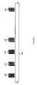
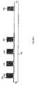
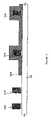
- FIG. 1shows a CMOS device having a plurality of FETS (i.e., NFETS and/or PFETS);
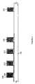
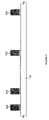
- FIG. 2shows a plurality of FETs, including a dense group of (i.e., a group of closely spaced) nFETs, on a semiconductor device;
- FIG. 3shows a thin tensile stress layer applied to the plurality of FETs from FIG. 2 , including the dense group of nFETs;
- FIG. 4shows the thin tensile stress layer removed from all areas except the dense group of nFETs
- FIG. 5shows the thin tensile stress layer on a dense group of nFETs and an isolated NFET, and a thick tensile layer on the isolated NFET;
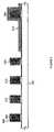
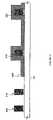
- FIG. 6shows a plurality of FETs, including a dense group of (i.e., a group of closely spaced) pFETs, on a semiconductor device;
- FIG. 7shows a thin compressive stress layer applied to the plurality of FETs from FIG. 5 , including the dense group of pFETs;
- FIG. 8shows the thin compressive stress layer removed from all areas except the dense group of pFETs
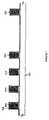
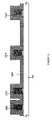
- FIG. 9shows a plurality of FETs, including a group of distantly spaced nFETs, on a semiconductor device
- FIG. 10shows a thick tensile stress layer applied to the plurality of FETs from FIG. 9 , including the group of distantly spaced nFETs;
- FIG. 11shows the thick tensile stress layer removed from all areas except the group of distantly spaced nFETs
- FIG. 12shows a plurality of FETs, including a group of distantly spaced pFETs, on a semiconductor device
- FIG. 13shows a thick compressive stress layer applied to the plurality of FETs from FIG. 12 , including the group of distantly spaced pFETs;
- FIG. 14shows the thick compressive stress layer removed from all areas except the group of distantly spaced pFETs.
- the inventionemploys selectively applied thin stressed films, such as tensile films, thin compressive films, and thick tensile films, to enhance electron and hole mobility in CMOS circuits.
- An exemplary process in accordance with the inventionentails steps of applying each film, and patterning for selectively removing the applied film from areas that would not experience performance benefit from the applied stressed film.
- a substrate 100 having a plurality of FETSi.e., NFETS and/or PFETS
- the substrate 100includes areas of different densities of nFETS and pFETs, including areas of high concentration or density 130 and areas of low concentration or density 140 .
- similar devicesare clustered; though the invention is applicable to devices having nFETs interspersed with pFETs, and vice versa.
- the high density area 130exhibits closely spaced FETs. In such an area, the distance from gate to gate may, for example, be 130 nanometers (nanometers). As used herein, a high density area refers to an area with closely spaced FETs, even if there are only two FETs in the area.
- the low density or isolated area 140exhibits FETs with a relatively substantial distance from gate to gate. In such an area, the distance from gate to gate may, for example, be 200 nanometers or greater.
- the substrate 100including the FETs 105 - 125 , may be fabricated in a conventional manner. While FIGS. 1 through 14 illustrate principles of exemplary implementations of the invention, they are not drawn to scale. Thus, the dimensions, proportions and spacings of device elements may differ from those depicted in the Figures.
- the stress layerinfluences what is considered a dense or isolated area.
- a dense areawould not be able to accommodate a thick stress layer without a substantial likelihood of void formation.
- the thicker the layerthe more space it requires to avoid undesirable void formation.
- some stress layer materials and depositing parametersmay be more conducive to void formation than others.
- an isolated areais able to accommodate a thick stress layer without a substantial likelihood of void formation. While layer thicknesses and distances between FETs are provided herein for illustrative purposes, those skilled in the art should appreciate that the invention is not limited to the specifically provided thicknesses and distances.
- Etch stop films (or layers) applied as stress layers in accordance with the inventionmay include refractory insulating material or materials with selective etch and physical properties.
- silicon nitride Si 3 N 4 or Si x N y , and/or silicon oxynitride Si x ON ymay be used for stress films. These materials may be grown or blanket deposited in a conventional manner, such as by chemical vapor deposition (CVD), plasma enhanced CVD or physical vapor deposition (PVD).
- CVDchemical vapor deposition
- PVDphysical vapor deposition
- Such filmscan be made with a well controlled thickness. Illustratively, the thickness range may be between 50 to 300 nanometers for a thick film, and 20 to 50 nanometers for a thin film.
- Etch stop films applied in accordance with the principles of the inventionact primarily as stress inducing layers.
- Stress in applied filmsmay be controlled in a conventional manner.
- the deposition pressure and/or plasma power and/or other deposition process parametersmay be varied illustratively, without limiting the scope of the invention, to achieve a tensile film exhibiting a tensile stress of approximately 700 MPa, the following CVD parameters may be used: a temperature of approximately 480° C., a pressure of approiximately 6.25 Torr, a spacing between the wafer and the electrode of 490 mils, a flow of 300 sccm of 2% dilute SiH 4 gas, 15 sccm NH 3 gas and 1060 sccm N 2 gas using RF power of 340 watts.
- the following CVD parametersmay be used: a temperature of approximately 480° C., a pressure of approiximately 5.75 Torr, a spacing between the wafer and the electrode of 395 mils, a flow of 3000 sccm of 2% dilute SiH 4 gas, 15 sccm NH 3 gas and 1060 sccm N 2 gas using RF power of 900 watts. Adjusting the deposition process parameters allows control over properties of the deposited material, including physical properties such as stress properties.
- FETs of different spacingsmay have stressed films of different thicknesses.
- closely spaced nFETsmay have a thin tensile film to enhance electron mobility and, thus, NFET performance, while avoiding formation of undesirable voids.
- closely spaced pFETsmay have a thin compressive film to enhance hole mobility and, thus, PFET performance, again while avoiding formation of undesirable voids.
- pFETs closely spaced to nFETswould also have thin stressed filns.
- nFETs having a minimum spacing large enough to avoid void formation when a thick film is appliedmay have a thick tensile film, while similarly spaced pFETs may have a thick compressive film.
- nFETs and pFETsmay each be further divided into more than two categories, with each category exhibiting a range of distances between FETs, and each category capable of accommodating a stressed film layer of a determined thickness without substantial risk of undesirable void formation.
- a stressed etch stop film of a determined thickness or range of thicknesseswill apply to each category.
- nFETs and pFETsmay each be divided into two categories, i.e., a dense category of closely spaced FETs 130 and an isolated category of distantly spaced FETs 140 , as shown in FIG. 1 .
- a dense group of (i.e., a group of closely spaced) nFETs 205 - 220 and an isolated FET 225are shown.
- the dense groupis spaced at about 130 nanometers or less, while the isolated FET 225 may exhibit a spacing of greater than 130 nanometers.
- a tensile stress layer 305is applied over the entire surface of the semiconductor device, as shown in FIG. 3 and discussed more fully below. Because the nFETs 205 - 220 are closely spaced, a thin tensile layer is applied. The applied tensile layer 305 is then removed, such as by masking and etching, from areas of the device that do not benefit from the imparted tensile stress as well as from areas that may benefit from an alternative stress layer, such as the isolated FET 225 .
- a thin oxide (e.g., SiO 2 ) liner(not shown) may be applied, to serve as an etch stop, before the tensile stress layer 305 is applied.
- the oxide linermay be approximately 1 to 10 nanometers in thickness. The oxide liner guards against unintended etching of the structure and elements beneath the applied liner and stress layers.
- a timed etchsuch as a timed dry etch, may be used to remove only the applied tensile layer from those areas of the substrate 100 that do not benefit from the imparted tensile stress.
- the thin stressed film 305may be comprised of, for example, Si 3 N 4 .
- the thin stressed filmmay also be, for example, Si x N y , and/or silicon oxynitride Si x ON y .
- the film 305may be blanket deposited over the entire surface of the substrate 100 in a conventional manner, such as by CVD, plasma enhanced CVD or PVD.
- the thin stressed filmmay have a thickness between 20 to 50 nanometers.
- the spacing of the closely packed nFETsis about 130 nanometers or less.
- the film 305may exhibit a tensile stress of approximately 600 to 1500 MPa (Mega-pascals).
- the film 305is thus configured to impart a tensile stress to the underlying areas.
- the thin tensile film 305is masked on locations where the dense nFETs 205 - 220 are present, and possibly where isolated nFETs are present, to allow removal from all other areas (e.g., FET 225 ) of the substrate 100 .
- the desired pattern of nFETsmay be transferred to an optical mask, as is well known in the art.
- the surface of the substrate 100may then be covered with photoresist.
- the resistmay then be exposed through the mask to radiation that changes its structure, polymerizing (i.e., cross linking) determined areas. Unpolymerzied regions may then be removed using a solvent, leaving the polymerized portions in tact.
- the thin tensile filmmay be removed by etching (e.g., by reactive ion etching using the patterned photoresist as a mask) from all areas (e.g., FET 225 ) except where the patterned nFETs (e.g., nFETs 205 - 220 ) are present, as shown in FIG. 4 .
- any remaining polymerized photoresistmay be removed using a wet process, such as sulfuric acid, or a dry process, such as O 2 plasma.
- the thin tensile layer 305may be left on isolated NFETS as shown in FIG. 5 .
- Additional thin (e.g., 20 to 50 nanometers) tensile layers and/or a thick (e.g., 50 to 500 nanometers) tensile layer 510may subsequently be added to the isolated nFETs, such as in a manner described more fully below, to impart greater tensile stress and thereby achieve further enhancement of electron mobility.
- the thin tensile layer 305may be removed from the isolated NFETS; in which case, the isolated nFETs may subsequently receive a thick (e.g., 50 to 500 nanometers) tensile layer to enhance electron mobility, as discussed more fully below.
- thin and thick compressive stress layersmay be applied to isolated pFETs, as discussed more fully below.
- oxide liner layer(not shown) may be deposited over the top surface of the entire device to serve as an etch stop, before the next stress layer is applied, as discussed below.
- the oxide linerguards against unintended etching of elements beneath it, including thin tensile stress layer 305 .
- a timed etchsuch as a timed dry etch, may be used to remove only the next layer from those areas of the substrate 100 that do not benefit from the imparted stress.
- a dense group of (i.e., a group of closely spaced) pFETs 605 - 620 and an isolated FET 625are shown.
- the dense group of pFETs 605 - 620is spaced at about 130 nanometers or less.
- a thin compressive stress layer 705is applied to the surface of the entire device, as shown in FIG. 7 .
- the thin compressive layer 705may be comprised of, for example, Si 3 N 4 .
- the thin compressive filmmay be Si x N y , and/or silicon oxynitride Si x ON y .
- the film 705may be blanket deposited over the entire surface of the substrate 100 in a conventional manner, such as by CVD, plasma enhanced CVD or PVD.
- the thin compressive filmmay have a thickness between 20 to 50 nanometers.
- the thin compressive film 705may exhibit a compressive stress of approximately ⁇ 600 to ⁇ 1500 MPa (Mega-pascals). The film 705 is thus configured to impart a compressive stress to underlying areas.
- the thin compressive film 705may be masked on locations where the dense pFETs 605 - 620 are present, and possibly where isolated pFETs are present, to allow removal from all other areas of the substrate 100 .
- the desired pattern of pFETsmay be transferred to an optical mask in a conventional manner.
- the surface of the substrate 100may then be covered with photoresist.
- the resistmay then be exposed through the mask to radiation that changes its structure, polymerizing (i.e., cross linking) determined areas. Unpolymerzied regions may then be removed using a solvent, leaving the polymerized portions in tact. Subsequent process steps (e.g., etching) will affect only the areas without polymerized photoresist.
- the thin compressive film 705may be removed by etching (e.g., by reactive ion etching using the patterned photoresist as a mask) from all areas (e.g., FET 625 ) except where the patterned pFETs (e.g., nFETs 605 - 620 ) are present, as shown in FIG. 8 .
- the polymerized photoresistmay be removed using a wet process, such as sulfuric acid, or a dry process, such as O 2 plasma.
- the thin compressive layer 705may be left on isolated pFETS. Additional thin (e.g., 20 to 50 nanometers) compressive layers and/or a thick (e.g., 50 to 500 nanometers) compressive layer may subsequently be added to isolated pFETs in a manner described above to impart greater compressive stress (e.g., ⁇ 600 to ⁇ 1500 MPa) and thereby achieve further enhancement of hole mobility.
- the thin compressive layer 705may be removed from the isolated pFETS 625 as shown in FIG. 8 ; in which case, the isolated pFETs 625 may subsequently receive a thick compressive layer to enhance hole mobility, as discussed more fully below.
- oxide liner layer(not shown) may be deposited over the top surface of the entire device to serve as an etch stop, before the next stress layer is applied, as discussed below.
- the oxide linerthus guards against unintended etching of elements beneath it, including thin compressive stress layer 705 .
- a timed etchsuch as a timed dry etch, may be used to remove only the next layer from those areas of the substrate 100 that do not benefit from the stress imparted by the next layer.
- a sparsely populated group of (i.e., a group of distantly spaced) nFETs 915 , 920 and a dense group of FETs 905 , 910are shown.
- the sparsely populated group of nFETsis spaced at about 130 nanometers or greater.
- a tensile stress layer 1005is applied to the surface of the entire substrate 100 , as shown in FIG. 10 .
- a thick stress layer 1005may be applied without substantial risk of void formation.
- FETs 905 and 910may have stress layer (not shown in FIG. 10 ) beneath layer 1005 .
- a stress layer suitable for FETs 905 and 910may be added after stress layer 1005 is added.
- the thick tensile film 1005may be comprised of, for example, Si 3 N 4 .
- the thick tensile filmmay also be, for example, Si x N y , and/or silicon oxynitride Si x ON y .
- the film 1005may be blanket deposited over the entire surface of the substrate 100 in a conventional manner, such as by CVD, plasma enhanced CVD or PVD.
- the thick tensile filmmay have a thickness between 50 to 300 nanometers.
- the thick tensile film 1005may exhibit a tensile stress of approximately 600 to 1500 MPa (Mega-pascals). The film 1005 is thus configured to impart a tensile stress to underlying areas.
- the thick tensile film 1005is masked on locations where the isolated nFETs 915 , 920 are present, to allow removal from all other areas of the substrate 100 .
- the desired pattern of nFETs 915 , 920may be transferred to an optical mask in a conventional manner.
- the surface of the substrate 100may then be covered with photoresist.
- the resistmay then be exposed through the mask to radiation that changes its structure, polymerizing (i.e., cross linking) determined areas. Unpolymerized regions may then be removed using a solvent, leaving the polymerized portions in tact. Subsequent process steps (e.g., etching) will affect only the areas without polymerized photoresist.
- the thick tensile film 1005may be removed by etching (e.g., by reactive ion etching using the patterned photoresist as a mask) from all areas (e.g., 905 , 910 ) except where the patterned nFETs 915 , 920 are present, as shown in FIG. 11 .
- the polymerized photoresistmay be removed using a wet process, such as sulfuric acid, or a dry process, such as O 2 plasma.
- oxide liner layer(not shown) may be deposited over the top surface of the entire device to serve as an etch stop, before the next stress layer is applied, as discussed below.
- the oxide linerguards against unintended etching of elements beneath it, including thick tensile stress layer 1005 .
- a timed etchsuch as a timed dry etch, may be used to remove only the next layer from those areas of the substrate 100 that do not benefit from the stress imparted by the next layer.
- a sparsely populated group of (i.e., a group of distantly spaced) pFETs 1215 , 1220 and a dense group of pFETs 1205 , 1210are shown.
- the distantly spaced pFETsmay have spacings of greater than 130 nanometers, while the closely spaced FETs 1205 , 1210 may have spacings of less than 130 nanometers.
- a compressive stress layer 1305is applied to the surface of the entire substrate 100 , as shown in FIG. 13 . Because the pFETs 1215 , 1220 are separated by a relatively substantial distance, a thick stress layer 1305 of about 50 to 500 nanometers in thickness may be applied without substantial risk of void formation.
- the thick compressive film 1305may be comprised of, for example, Si 3 N 4 .
- the thick compressive filmmay also be, for example, Si x N y , and/or silicon oxynitride Si x ON y .
- the film 1305may be blanket deposited over the entire surface of the substrate 100 in a conventional manner, such as by CVD, plasma enhanced CVD or PVD.
- the thick compressive filmmay have a thickness between 50 to 300 nanometers.
- the thick compressive film 1305may exhibit a compressive stress of approximately ⁇ 600 to ⁇ 1500 MPa (Mega-pascals). The film 1305 is thus configured to impart a compressive stress to underlying areas.
- the thick compressive film 1305is masked on locations where the isolated pFETs 1215 , 1220 are present, to allow removal from all other areas (e.g., 1205 , 1210 ) of the substrate 100 .
- the desired pattern of pFETs 1215 , 1220may be transferred to an optical mask in a conventional manner.
- the surface of the substrate 100may then be covered with photoresist.
- the resistmay then be exposed through the mask to radiation that changes its structure, polymerizing (i.e., cross linking) determined areas. Unpolymerized regions may then be removed using a solvent, leaving the polymerized portions in tact. Subsequent process steps (e.g., etching) will affect only the areas without polymerized photoresist.
- the thick compressive film 1305may be removed by etching from all areas except where the patterned pFETs 1215 , 1220 are present, as shown in FIG. 14 .
- the polymerized photoresistmay be removed using a wet process, such as sulfuric acid, or a dry process, such as O 2 plasma.
- Compressive layersmay be applied before or after tensile layers.
- Thick layersmay be applied before or after thin layers.
- thick layersmay be reduced via timed etching to produce thin stress layers over a densely populated areas.
- a thick compressive layermay be applied for all pFETs.
- the compressive layermay then be removed from all areas that do not benefit from compressive stress such as, for example, areas populated with nFETs. Such removal may be carried out in the manner described above.
- the compressive layermay be reduced in thickness through a wet or dry timed etch. The reduced thickness may be, for example, 20 to 50 nanometers. Isolated pFET areas may be protected with a photoresist or etch stop to avoid undesired removal and thinning of the compressive layer.
- thin compressive layersmay be applied and built-up in successive layers to achieve desired thicknesses.
- a thin tensile layer of approximately 20 to 50 nanometersmay be applied for all nFETs.
- one or more additional thin tensile layersmay be applied for isolated nFETs.
- the additional thin tensile layersmay be removed from all areas that would be susceptible to void formation or that do not benefit from tensile stress, such as areas populated by pFETs. Such removal may be carried out in the manner described above.
Landscapes
- Metal-Oxide And Bipolar Metal-Oxide Semiconductor Integrated Circuits (AREA)
- Insulated Gate Type Field-Effect Transistor (AREA)
- Thin Film Transistor (AREA)
Abstract
Description
Claims (23)
Priority Applications (2)
| Application Number | Priority Date | Filing Date | Title |
|---|---|---|---|
| US11/244,291US7285826B2 (en) | 2003-11-06 | 2005-10-06 | High mobility CMOS circuits |
| US11/863,757US8013392B2 (en) | 2003-11-06 | 2007-09-28 | High mobility CMOS circuits |
Applications Claiming Priority (2)
| Application Number | Priority Date | Filing Date | Title |
|---|---|---|---|
| US10/701,526US7015082B2 (en) | 2003-11-06 | 2003-11-06 | High mobility CMOS circuits |
| US11/244,291US7285826B2 (en) | 2003-11-06 | 2005-10-06 | High mobility CMOS circuits |
Related Parent Applications (1)
| Application Number | Title | Priority Date | Filing Date |
|---|---|---|---|
| US10/701,526ContinuationUS7015082B2 (en) | 2003-11-06 | 2003-11-06 | High mobility CMOS circuits |
Related Child Applications (1)
| Application Number | Title | Priority Date | Filing Date |
|---|---|---|---|
| US11/863,757ContinuationUS8013392B2 (en) | 2003-11-06 | 2007-09-28 | High mobility CMOS circuits |
Publications (2)
| Publication Number | Publication Date |
|---|---|
| US20060027868A1 US20060027868A1 (en) | 2006-02-09 |
| US7285826B2true US7285826B2 (en) | 2007-10-23 |
Family
ID=34551445
Family Applications (3)
| Application Number | Title | Priority Date | Filing Date |
|---|---|---|---|
| US10/701,526Expired - Fee RelatedUS7015082B2 (en) | 2003-11-06 | 2003-11-06 | High mobility CMOS circuits |
| US11/244,291Expired - LifetimeUS7285826B2 (en) | 2003-11-06 | 2005-10-06 | High mobility CMOS circuits |
| US11/863,757Expired - Fee RelatedUS8013392B2 (en) | 2003-11-06 | 2007-09-28 | High mobility CMOS circuits |
Family Applications Before (1)
| Application Number | Title | Priority Date | Filing Date |
|---|---|---|---|
| US10/701,526Expired - Fee RelatedUS7015082B2 (en) | 2003-11-06 | 2003-11-06 | High mobility CMOS circuits |
Family Applications After (1)
| Application Number | Title | Priority Date | Filing Date |
|---|---|---|---|
| US11/863,757Expired - Fee RelatedUS8013392B2 (en) | 2003-11-06 | 2007-09-28 | High mobility CMOS circuits |
Country Status (1)
| Country | Link |
|---|---|
| US (3) | US7015082B2 (en) |
Cited By (2)
| Publication number | Priority date | Publication date | Assignee | Title |
|---|---|---|---|---|
| US20100269075A1 (en)* | 2009-04-20 | 2010-10-21 | William Robert Tonti | Method and system for selective stress enablement in simulation modeling |
| US20180110826A1 (en)* | 2013-04-18 | 2018-04-26 | The United States of America, as represented by the Secretary of the Army, on behalf of the United | Therapeutic compositions for neutralizing type i interferons, and methods of use |
Families Citing this family (77)
| Publication number | Priority date | Publication date | Assignee | Title |
|---|---|---|---|---|
| US7022561B2 (en)* | 2002-12-02 | 2006-04-04 | Taiwan Semiconductor Manufacturing Company, Ltd. | CMOS device |
| US7410846B2 (en)* | 2003-09-09 | 2008-08-12 | International Business Machines Corporation | Method for reduced N+ diffusion in strained Si on SiGe substrate |
| US6887751B2 (en) | 2003-09-12 | 2005-05-03 | International Business Machines Corporation | MOSFET performance improvement using deformation in SOI structure |
| US6872641B1 (en)* | 2003-09-23 | 2005-03-29 | International Business Machines Corporation | Strained silicon on relaxed sige film with uniform misfit dislocation density |
| US7144767B2 (en)* | 2003-09-23 | 2006-12-05 | International Business Machines Corporation | NFETs using gate induced stress modulation |
| US7119403B2 (en)* | 2003-10-16 | 2006-10-10 | International Business Machines Corporation | High performance strained CMOS devices |
| US7037770B2 (en)* | 2003-10-20 | 2006-05-02 | International Business Machines Corporation | Method of manufacturing strained dislocation-free channels for CMOS |
| US7303949B2 (en) | 2003-10-20 | 2007-12-04 | International Business Machines Corporation | High performance stress-enhanced MOSFETs using Si:C and SiGe epitaxial source/drain and method of manufacture |
| US8008724B2 (en)* | 2003-10-30 | 2011-08-30 | International Business Machines Corporation | Structure and method to enhance both nFET and pFET performance using different kinds of stressed layers |
| US7129126B2 (en)* | 2003-11-05 | 2006-10-31 | International Business Machines Corporation | Method and structure for forming strained Si for CMOS devices |
| US7015082B2 (en)* | 2003-11-06 | 2006-03-21 | International Business Machines Corporation | High mobility CMOS circuits |
| US7029964B2 (en) | 2003-11-13 | 2006-04-18 | International Business Machines Corporation | Method of manufacturing a strained silicon on a SiGe on SOI substrate |
| US7122849B2 (en) | 2003-11-14 | 2006-10-17 | International Business Machines Corporation | Stressed semiconductor device structures having granular semiconductor material |
| US7247534B2 (en) | 2003-11-19 | 2007-07-24 | International Business Machines Corporation | Silicon device on Si:C-OI and SGOI and method of manufacture |
| US7198995B2 (en)* | 2003-12-12 | 2007-04-03 | International Business Machines Corporation | Strained finFETs and method of manufacture |
| US7247912B2 (en)* | 2004-01-05 | 2007-07-24 | International Business Machines Corporation | Structures and methods for making strained MOSFETs |
| US7202132B2 (en) | 2004-01-16 | 2007-04-10 | International Business Machines Corporation | Protecting silicon germanium sidewall with silicon for strained silicon/silicon germanium MOSFETs |
| US7381609B2 (en)* | 2004-01-16 | 2008-06-03 | International Business Machines Corporation | Method and structure for controlling stress in a transistor channel |
| US7118999B2 (en)* | 2004-01-16 | 2006-10-10 | International Business Machines Corporation | Method and apparatus to increase strain effect in a transistor channel |
| US7205206B2 (en)* | 2004-03-03 | 2007-04-17 | International Business Machines Corporation | Method of fabricating mobility enhanced CMOS devices |
| US7223994B2 (en)* | 2004-06-03 | 2007-05-29 | International Business Machines Corporation | Strained Si on multiple materials for bulk or SOI substrates |
| TWI463526B (en)* | 2004-06-24 | 2014-12-01 | Ibm | Method for improving stress-induced CMOS components and components prepared by the method |
| US7288443B2 (en)* | 2004-06-29 | 2007-10-30 | International Business Machines Corporation | Structures and methods for manufacturing p-type MOSFET with graded embedded silicon-germanium source-drain and/or extension |
| US6991998B2 (en)* | 2004-07-02 | 2006-01-31 | International Business Machines Corporation | Ultra-thin, high quality strained silicon-on-insulator formed by elastic strain transfer |
| US7384829B2 (en) | 2004-07-23 | 2008-06-10 | International Business Machines Corporation | Patterned strained semiconductor substrate and device |
| US7173312B2 (en)* | 2004-12-15 | 2007-02-06 | International Business Machines Corporation | Structure and method to generate local mechanical gate stress for MOSFET channel mobility modification |
| US20060160317A1 (en)* | 2005-01-18 | 2006-07-20 | International Business Machines Corporation | Structure and method to enhance stress in a channel of cmos devices using a thin gate |
| US7256081B2 (en)* | 2005-02-01 | 2007-08-14 | International Business Machines Corporation | Structure and method to induce strain in a semiconductor device channel with stressed film under the gate |
| US7224033B2 (en) | 2005-02-15 | 2007-05-29 | International Business Machines Corporation | Structure and method for manufacturing strained FINFET |
| US7545004B2 (en)* | 2005-04-12 | 2009-06-09 | International Business Machines Corporation | Method and structure for forming strained devices |
| US8138104B2 (en)* | 2005-05-26 | 2012-03-20 | Applied Materials, Inc. | Method to increase silicon nitride tensile stress using nitrogen plasma in-situ treatment and ex-situ UV cure |
| US7566655B2 (en)* | 2005-05-26 | 2009-07-28 | Applied Materials, Inc. | Integration process for fabricating stressed transistor structure |
| US8129290B2 (en)* | 2005-05-26 | 2012-03-06 | Applied Materials, Inc. | Method to increase tensile stress of silicon nitride films using a post PECVD deposition UV cure |
| US7858458B2 (en) | 2005-06-14 | 2010-12-28 | Micron Technology, Inc. | CMOS fabrication |
| US20070013070A1 (en)* | 2005-06-23 | 2007-01-18 | Liang Mong S | Semiconductor devices and methods of manufacture thereof |
| US20070010070A1 (en)* | 2005-07-05 | 2007-01-11 | International Business Machines Corporation | Fabrication of strained semiconductor-on-insulator (ssoi) structures by using strained insulating layers |
| US7297584B2 (en)* | 2005-10-07 | 2007-11-20 | Samsung Electronics Co., Ltd. | Methods of fabricating semiconductor devices having a dual stress liner |
| US7615432B2 (en)* | 2005-11-02 | 2009-11-10 | Samsung Electronics Co., Ltd. | HDP/PECVD methods of fabricating stress nitride structures for field effect transistors |
| US7655511B2 (en) | 2005-11-03 | 2010-02-02 | International Business Machines Corporation | Gate electrode stress control for finFET performance enhancement |
| US7564081B2 (en) | 2005-11-30 | 2009-07-21 | International Business Machines Corporation | finFET structure with multiply stressed gate electrode |
| US7635620B2 (en) | 2006-01-10 | 2009-12-22 | International Business Machines Corporation | Semiconductor device structure having enhanced performance FET device |
| US20070158743A1 (en)* | 2006-01-11 | 2007-07-12 | International Business Machines Corporation | Thin silicon single diffusion field effect transistor for enhanced drive performance with stress film liners |
| JP2007207837A (en) | 2006-01-31 | 2007-08-16 | Toshiba Corp | Semiconductor device and manufacturing method of semiconductor device |
| US7691698B2 (en) | 2006-02-21 | 2010-04-06 | International Business Machines Corporation | Pseudomorphic Si/SiGe/Si body device with embedded SiGe source/drain |
| US20070249129A1 (en)* | 2006-04-21 | 2007-10-25 | Freescale Semiconductor, Inc. | STI stressor integration for minimal phosphoric exposure and divot-free topography |
| US7528029B2 (en) | 2006-04-21 | 2009-05-05 | Freescale Semiconductor, Inc. | Stressor integration and method thereof |
| US7608489B2 (en)* | 2006-04-28 | 2009-10-27 | International Business Machines Corporation | High performance stress-enhance MOSFET and method of manufacture |
| US7521307B2 (en)* | 2006-04-28 | 2009-04-21 | International Business Machines Corporation | CMOS structures and methods using self-aligned dual stressed layers |
| US7615418B2 (en)* | 2006-04-28 | 2009-11-10 | International Business Machines Corporation | High performance stress-enhance MOSFET and method of manufacture |
| US8853746B2 (en) | 2006-06-29 | 2014-10-07 | International Business Machines Corporation | CMOS devices with stressed channel regions, and methods for fabricating the same |
| US7678636B2 (en)* | 2006-06-29 | 2010-03-16 | Taiwan Semiconductor Manufacturing Company, Ltd. | Selective formation of stress memorization layer |
| US7790540B2 (en) | 2006-08-25 | 2010-09-07 | International Business Machines Corporation | Structure and method to use low k stress liner to reduce parasitic capacitance |
| US8754446B2 (en) | 2006-08-30 | 2014-06-17 | International Business Machines Corporation | Semiconductor structure having undercut-gate-oxide gate stack enclosed by protective barrier material |
| US7462522B2 (en)* | 2006-08-30 | 2008-12-09 | International Business Machines Corporation | Method and structure for improving device performance variation in dual stress liner technology |
| KR100809335B1 (en)* | 2006-09-28 | 2008-03-05 | 삼성전자주식회사 | Semiconductor device and manufacturing method thereof |
| US20080087965A1 (en)* | 2006-10-11 | 2008-04-17 | International Business Machines Corporation | Structure and method of forming transistor density based stress layers in cmos devices |
| US20080116521A1 (en)* | 2006-11-16 | 2008-05-22 | Samsung Electronics Co., Ltd | CMOS Integrated Circuits that Utilize Insulating Layers with High Stress Characteristics to Improve NMOS and PMOS Transistor Carrier Mobilities and Methods of Forming Same |
| US7932178B2 (en)* | 2006-12-28 | 2011-04-26 | Globalfoundries Singapore Pte. Ltd. | Integrated circuit having a plurality of MOSFET devices |
| US20080217700A1 (en)* | 2007-03-11 | 2008-09-11 | Doris Bruce B | Mobility Enhanced FET Devices |
| US7534678B2 (en)* | 2007-03-27 | 2009-05-19 | Samsung Electronics Co., Ltd. | Methods of forming CMOS integrated circuit devices having stressed NMOS and PMOS channel regions therein and circuits formed thereby |
| US7521380B2 (en)* | 2007-04-23 | 2009-04-21 | Advanced Micro Devices, Inc. | Methods for fabricating a stress enhanced semiconductor device having narrow pitch and wide pitch transistors |
| US7923373B2 (en) | 2007-06-04 | 2011-04-12 | Micron Technology, Inc. | Pitch multiplication using self-assembling materials |
| US7755926B2 (en)* | 2007-06-13 | 2010-07-13 | International Business Machines Corporation | 3-D SRAM array to improve stability and performance |
| US20080310220A1 (en)* | 2007-06-13 | 2008-12-18 | International Business Machines Corporation | 3-d sram array to improve stability and performance |
| US7615435B2 (en)* | 2007-07-31 | 2009-11-10 | International Business Machines Corporation | Semiconductor device and method of manufacture |
| US20090050972A1 (en)* | 2007-08-20 | 2009-02-26 | Richard Lindsay | Strained Semiconductor Device and Method of Making Same |
| US7902082B2 (en)* | 2007-09-20 | 2011-03-08 | Samsung Electronics Co., Ltd. | Method of forming field effect transistors using diluted hydrofluoric acid to remove sacrificial nitride spacers |
| US8115254B2 (en) | 2007-09-25 | 2012-02-14 | International Business Machines Corporation | Semiconductor-on-insulator structures including a trench containing an insulator stressor plug and method of fabricating same |
| US20090095991A1 (en)* | 2007-10-11 | 2009-04-16 | International Business Machines Corporation | Method of forming strained mosfet devices using phase transformable materials |
| US7923365B2 (en)* | 2007-10-17 | 2011-04-12 | Samsung Electronics Co., Ltd. | Methods of forming field effect transistors having stress-inducing sidewall insulating spacers thereon |
| US8492846B2 (en) | 2007-11-15 | 2013-07-23 | International Business Machines Corporation | Stress-generating shallow trench isolation structure having dual composition |
| US8598006B2 (en)* | 2010-03-16 | 2013-12-03 | International Business Machines Corporation | Strain preserving ion implantation methods |
| US8937369B2 (en)* | 2012-10-01 | 2015-01-20 | United Microelectronics Corp. | Transistor with non-uniform stress layer with stress concentrated regions |
| US9018108B2 (en) | 2013-01-25 | 2015-04-28 | Applied Materials, Inc. | Low shrinkage dielectric films |
| CN104051338B (en)* | 2013-03-12 | 2016-12-28 | 旺宏电子股份有限公司 | Semiconductor structure and manufacturing method thereof |
| US9184096B2 (en)* | 2013-03-13 | 2015-11-10 | Macronix International Co., Ltd. | Semiconductor structure and manufacturing method for the same |
| US10043903B2 (en) | 2015-12-21 | 2018-08-07 | Samsung Electronics Co., Ltd. | Semiconductor devices with source/drain stress liner |
Citations (88)
| Publication number | Priority date | Publication date | Assignee | Title |
|---|---|---|---|---|
| US3602841A (en) | 1970-06-18 | 1971-08-31 | Ibm | High frequency bulk semiconductor amplifiers and oscillators |
| US4665415A (en) | 1985-04-24 | 1987-05-12 | International Business Machines Corporation | Semiconductor device with hole conduction via strained lattice |
| JPS6476755A (en) | 1987-09-18 | 1989-03-22 | Hitachi Ltd | Semiconductor device |
| US4853076A (en) | 1983-12-29 | 1989-08-01 | Massachusetts Institute Of Technology | Semiconductor thin films |
| US4855245A (en) | 1985-09-13 | 1989-08-08 | Siemens Aktiengesellschaft | Method of manufacturing integrated circuit containing bipolar and complementary MOS transistors on a common substrate |
| US4952524A (en) | 1989-05-05 | 1990-08-28 | At&T Bell Laboratories | Semiconductor device manufacture including trench formation |
| US4958213A (en) | 1987-12-07 | 1990-09-18 | Texas Instruments Incorporated | Method for forming a transistor base region under thick oxide |
| US5006913A (en) | 1988-11-05 | 1991-04-09 | Mitsubishi Denki Kabushiki Kaisha | Stacked type semiconductor device |
| US5060030A (en) | 1990-07-18 | 1991-10-22 | Raytheon Company | Pseudomorphic HEMT having strained compensation layer |
| US5081513A (en) | 1991-02-28 | 1992-01-14 | Xerox Corporation | Electronic device with recovery layer proximate to active layer |
| US5108843A (en) | 1988-11-30 | 1992-04-28 | Ricoh Company, Ltd. | Thin film semiconductor and process for producing the same |
| US5134085A (en) | 1991-11-21 | 1992-07-28 | Micron Technology, Inc. | Reduced-mask, split-polysilicon CMOS process, incorporating stacked-capacitor cells, for fabricating multi-megabit dynamic random access memories |
| US5310446A (en) | 1990-01-10 | 1994-05-10 | Ricoh Company, Ltd. | Method for producing semiconductor film |
| US5354695A (en) | 1992-04-08 | 1994-10-11 | Leedy Glenn J | Membrane dielectric isolation IC fabrication |
| US5371399A (en) | 1991-06-14 | 1994-12-06 | International Business Machines Corporation | Compound semiconductor having metallic inclusions and devices fabricated therefrom |
| US5391510A (en) | 1992-02-28 | 1995-02-21 | International Business Machines Corporation | Formation of self-aligned metal gate FETs using a benignant removable gate material during high temperature steps |
| US5459346A (en) | 1988-06-28 | 1995-10-17 | Ricoh Co., Ltd. | Semiconductor substrate with electrical contact in groove |
| US5557122A (en) | 1995-05-12 | 1996-09-17 | Alliance Semiconductors Corporation | Semiconductor electrode having improved grain structure and oxide growth properties |
| US5561302A (en) | 1994-09-26 | 1996-10-01 | Motorola, Inc. | Enhanced mobility MOSFET device and method |
| US5670798A (en) | 1995-03-29 | 1997-09-23 | North Carolina State University | Integrated heterostructures of Group III-V nitride semiconductor materials including epitaxial ohmic contact non-nitride buffer layer and methods of fabricating same |
| US5679965A (en) | 1995-03-29 | 1997-10-21 | North Carolina State University | Integrated heterostructures of Group III-V nitride semiconductor materials including epitaxial ohmic contact, non-nitride buffer layer and methods of fabricating same |
| US5861651A (en) | 1997-02-28 | 1999-01-19 | Lucent Technologies Inc. | Field effect devices and capacitors with improved thin film dielectrics and method for making same |
| US5880040A (en) | 1996-04-15 | 1999-03-09 | Macronix International Co., Ltd. | Gate dielectric based on oxynitride grown in N2 O and annealed in NO |
| US5940736A (en) | 1997-03-11 | 1999-08-17 | Lucent Technologies Inc. | Method for forming a high quality ultrathin gate oxide layer |
| US5960297A (en) | 1997-07-02 | 1999-09-28 | Kabushiki Kaisha Toshiba | Shallow trench isolation structure and method of forming the same |
| US5989978A (en) | 1998-07-16 | 1999-11-23 | Chartered Semiconductor Manufacturing, Ltd. | Shallow trench isolation of MOSFETS with reduced corner parasitic currents |
| US6008126A (en) | 1992-04-08 | 1999-12-28 | Elm Technology Corporation | Membrane dielectric isolation IC fabrication |
| US6025280A (en) | 1997-04-28 | 2000-02-15 | Lucent Technologies Inc. | Use of SiD4 for deposition of ultra thin and controllable oxides |
| US6066545A (en) | 1997-12-09 | 2000-05-23 | Texas Instruments Incorporated | Birdsbeak encroachment using combination of wet and dry etch for isolation nitride |
| US6090684A (en) | 1998-07-31 | 2000-07-18 | Hitachi, Ltd. | Method for manufacturing semiconductor device |
| US6107143A (en) | 1998-03-02 | 2000-08-22 | Samsung Electronics Co., Ltd. | Method for forming a trench isolation structure in an integrated circuit |
| US6117722A (en) | 1999-02-18 | 2000-09-12 | Taiwan Semiconductor Manufacturing Company | SRAM layout for relaxing mechanical stress in shallow trench isolation technology and method of manufacture thereof |
| US6133071A (en) | 1997-10-15 | 2000-10-17 | Nec Corporation | Semiconductor device with plate heat sink free from cracks due to thermal stress and process for assembling it with package |
| US6165383A (en) | 1998-04-10 | 2000-12-26 | Organic Display Technology | Useful precursors for organic electroluminescent materials and devices made from such materials |
| US6221735B1 (en) | 2000-02-15 | 2001-04-24 | Philips Semiconductors, Inc. | Method for eliminating stress induced dislocations in CMOS devices |
| US6228694B1 (en) | 1999-06-28 | 2001-05-08 | Intel Corporation | Method of increasing the mobility of MOS transistors by use of localized stress regions |
| US6235574B1 (en)* | 1999-03-22 | 2001-05-22 | Infineon North America Corp. | High performance DRAM and method of manufacture |
| US6255169B1 (en) | 1999-02-22 | 2001-07-03 | Advanced Micro Devices, Inc. | Process for fabricating a high-endurance non-volatile memory device |
| US6261964B1 (en) | 1997-03-14 | 2001-07-17 | Micron Technology, Inc. | Material removal method for forming a structure |
| US6265317B1 (en) | 2001-01-09 | 2001-07-24 | Taiwan Semiconductor Manufacturing Company | Top corner rounding for shallow trench isolation |
| US20010009784A1 (en) | 1998-01-09 | 2001-07-26 | Yanjun Ma | Structure and method of making a sub-micron MOS transistor |
| US6274444B1 (en) | 1999-07-30 | 2001-08-14 | United Microelectronics Corp. | Method for forming mosfet |
| US6281532B1 (en) | 1999-06-28 | 2001-08-28 | Intel Corporation | Technique to obtain increased channel mobilities in NMOS transistors by gate electrode engineering |
| US6284623B1 (en) | 1999-10-25 | 2001-09-04 | Peng-Fei Zhang | Method of fabricating semiconductor devices using shallow trench isolation with reduced narrow channel effect |
| US6284626B1 (en) | 1999-04-06 | 2001-09-04 | Vantis Corporation | Angled nitrogen ion implantation for minimizing mechanical stress on side walls of an isolation trench |
| US6319794B1 (en) | 1998-10-14 | 2001-11-20 | International Business Machines Corporation | Structure and method for producing low leakage isolation devices |
| US6361885B1 (en) | 1998-04-10 | 2002-03-26 | Organic Display Technology | Organic electroluminescent materials and device made from such materials |
| US6362082B1 (en) | 1999-06-28 | 2002-03-26 | Intel Corporation | Methodology for control of short channel effects in MOS transistors |
| US6368931B1 (en) | 2000-03-27 | 2002-04-09 | Intel Corporation | Thin tensile layers in shallow trench isolation and method of making same |
| US20020063292A1 (en) | 2000-11-29 | 2002-05-30 | Mark Armstrong | CMOS fabrication process utilizing special transistor orientation |
| US6403486B1 (en) | 2001-04-30 | 2002-06-11 | Taiwan Semiconductor Manufacturing Company | Method for forming a shallow trench isolation |
| US6403975B1 (en) | 1996-04-09 | 2002-06-11 | Max-Planck Gesellschaft Zur Forderung Der Wissenschafteneev | Semiconductor components, in particular photodetectors, light emitting diodes, optical modulators and waveguides with multilayer structures grown on silicon substrates |
| US6406973B1 (en) | 1999-06-29 | 2002-06-18 | Hyundai Electronics Industries Co., Ltd. | Transistor in a semiconductor device and method of manufacturing the same |
| US20020086497A1 (en) | 2000-12-30 | 2002-07-04 | Kwok Siang Ping | Beaker shape trench with nitride pull-back for STI |
| US20020086472A1 (en) | 2000-12-29 | 2002-07-04 | Brian Roberds | Technique to obtain high mobility channels in MOS transistors by forming a strain layer on an underside of a channel |
| US20020090791A1 (en) | 1999-06-28 | 2002-07-11 | Brian S. Doyle | Method for reduced capacitance interconnect system using gaseous implants into the ild |
| US6461936B1 (en) | 2002-01-04 | 2002-10-08 | Infineon Technologies Ag | Double pullback method of filling an isolation trench |
| US6476462B2 (en) | 1999-12-28 | 2002-11-05 | Texas Instruments Incorporated | MOS-type semiconductor device and method for making same |
| US6483171B1 (en) | 1999-08-13 | 2002-11-19 | Micron Technology, Inc. | Vertical sub-micron CMOS transistors on (110), (111), (311), (511), and higher order surfaces of bulk, SOI and thin film structures and method of forming same |
| US6483154B1 (en)* | 2000-10-05 | 2002-11-19 | Advanced Micro Devices, Inc. | Nitrogen oxide plasma treatment for reduced nickel silicide bridging |
| US6493497B1 (en) | 2000-09-26 | 2002-12-10 | Motorola, Inc. | Electro-optic structure and process for fabricating same |
| US6498358B1 (en) | 2001-07-20 | 2002-12-24 | Motorola, Inc. | Structure and method for fabricating an electro-optic system having an electrochromic diffraction grating |
| US6501121B1 (en) | 2000-11-15 | 2002-12-31 | Motorola, Inc. | Semiconductor structure |
| US6506652B2 (en) | 1998-11-13 | 2003-01-14 | Intel Corporation | Method of recessing spacers to improved salicide resistance on polysilicon gates |
| US20030032261A1 (en) | 2001-08-08 | 2003-02-13 | Ling-Yen Yeh | Method of preventing threshold voltage of MOS transistor from being decreased by shallow trench isolation formation |
| US20030040158A1 (en) | 2001-08-21 | 2003-02-27 | Nec Corporation | Semiconductor device and method of fabricating the same |
| US6531740B2 (en) | 2001-07-17 | 2003-03-11 | Motorola, Inc. | Integrated impedance matching and stability network |
| US6531369B1 (en) | 2000-03-01 | 2003-03-11 | Applied Micro Circuits Corporation | Heterojunction bipolar transistor (HBT) fabrication using a selectively deposited silicon germanium (SiGe) |
| US20030057184A1 (en) | 2001-09-22 | 2003-03-27 | Shiuh-Sheng Yu | Method for pull back SiN to increase rounding effect in a shallow trench isolation process |
| US20030067035A1 (en) | 2001-09-28 | 2003-04-10 | Helmut Tews | Gate processing method with reduced gate oxide corner and edge thinning |
| US6573172B1 (en)* | 2002-09-16 | 2003-06-03 | Advanced Micro Devices, Inc. | Methods for improving carrier mobility of PMOS and NMOS devices |
| US6717216B1 (en) | 2002-12-12 | 2004-04-06 | International Business Machines Corporation | SOI based field effect transistor having a compressive film in undercut area under the channel and a method of making the device |
| US20040135234A1 (en) | 2002-11-05 | 2004-07-15 | Stmicroelectronics Sa | Semiconductor device with MOS transistors with an etch-stop layer having an improved residual stress level and method for fabricating such a semiconductor device |
| US6825529B2 (en) | 2002-12-12 | 2004-11-30 | International Business Machines Corporation | Stress inducing spacers |
| US20040238914A1 (en) | 2003-05-30 | 2004-12-02 | International Business Machines Corporation | STI stress modification by nitrogen plasma treatment for improving performance in small width devices |
| US6831292B2 (en) | 2001-09-21 | 2004-12-14 | Amberwave Systems Corporation | Semiconductor structures employing strained material layers with defined impurity gradients and methods for fabricating same |
| US20040262784A1 (en) | 2003-06-30 | 2004-12-30 | International Business Machines Corporation | High performance cmos device structures and method of manufacture |
| US20050082634A1 (en) | 2003-10-16 | 2005-04-21 | International Business Machines Corporation | High performance strained cmos devices |
| US20050093030A1 (en) | 2003-10-30 | 2005-05-05 | Doris Bruce B. | Structure and method to enhance both nFET and pFET performance using different kinds of stressed layers |
| US20050098829A1 (en) | 2003-11-06 | 2005-05-12 | Doris Bruce B. | High mobility CMOS circuits |
| US20050106799A1 (en) | 2003-11-14 | 2005-05-19 | International Business Machines Corporation | Stressed semiconductor device structures having granular semiconductor material |
| US20050145954A1 (en) | 2004-01-05 | 2005-07-07 | International Business Machines Corporation | Structures and methods for making strained mosfets |
| US20050194699A1 (en) | 2004-03-03 | 2005-09-08 | International Business Machines Corporation | Mobility enhanced cmos devices |
| US20050236668A1 (en) | 2004-04-23 | 2005-10-27 | International Business Machines Corporation | STRUCTURES AND METHODS FOR MANUFACTURING OF DISLOCATION FREE STRESSED CHANNELS IN BULK SILICON AND SOI CMOS DEVICES BY GATE STRESS ENGINEERING WITH SiGe AND/OR Si:C |
| US20050245017A1 (en) | 2003-10-30 | 2005-11-03 | Belyansky Michael P | Structure and method to improve channel mobility by gate electrode stress modification |
| US6974981B2 (en) | 2002-12-12 | 2005-12-13 | International Business Machines Corporation | Isolation structures for imposing stress patterns |
| US20060057787A1 (en) | 2002-11-25 | 2006-03-16 | Doris Bruce B | Strained finfet cmos device structures |
| US20060060925A1 (en) | 2004-09-17 | 2006-03-23 | International Business Machines Corporation | Semiconductor device structure with active regions having different surface directions and methods |
Family Cites Families (3)
| Publication number | Priority date | Publication date | Assignee | Title |
|---|---|---|---|---|
| DE10041934A1 (en)* | 2000-08-25 | 2002-03-07 | Roland Man Druckmasch | Method and device for coating printed products |
| JP2003086708A (en)* | 2000-12-08 | 2003-03-20 | Hitachi Ltd | Semiconductor device and manufacturing method thereof |
| JP4173672B2 (en)* | 2002-03-19 | 2008-10-29 | 株式会社ルネサステクノロジ | Semiconductor device and manufacturing method thereof |
- 2003
- 2003-11-06USUS10/701,526patent/US7015082B2/ennot_activeExpired - Fee Related
- 2005
- 2005-10-06USUS11/244,291patent/US7285826B2/ennot_activeExpired - Lifetime
- 2007
- 2007-09-28USUS11/863,757patent/US8013392B2/ennot_activeExpired - Fee Related
Patent Citations (108)
| Publication number | Priority date | Publication date | Assignee | Title |
|---|---|---|---|---|
| US3602841A (en) | 1970-06-18 | 1971-08-31 | Ibm | High frequency bulk semiconductor amplifiers and oscillators |
| US4853076A (en) | 1983-12-29 | 1989-08-01 | Massachusetts Institute Of Technology | Semiconductor thin films |
| US4665415A (en) | 1985-04-24 | 1987-05-12 | International Business Machines Corporation | Semiconductor device with hole conduction via strained lattice |
| US4855245A (en) | 1985-09-13 | 1989-08-08 | Siemens Aktiengesellschaft | Method of manufacturing integrated circuit containing bipolar and complementary MOS transistors on a common substrate |
| JPS6476755A (en) | 1987-09-18 | 1989-03-22 | Hitachi Ltd | Semiconductor device |
| US4958213A (en) | 1987-12-07 | 1990-09-18 | Texas Instruments Incorporated | Method for forming a transistor base region under thick oxide |
| US5565697A (en) | 1988-06-28 | 1996-10-15 | Ricoh Company, Ltd. | Semiconductor structure having island forming grooves |
| US5459346A (en) | 1988-06-28 | 1995-10-17 | Ricoh Co., Ltd. | Semiconductor substrate with electrical contact in groove |
| US5006913A (en) | 1988-11-05 | 1991-04-09 | Mitsubishi Denki Kabushiki Kaisha | Stacked type semiconductor device |
| US5108843A (en) | 1988-11-30 | 1992-04-28 | Ricoh Company, Ltd. | Thin film semiconductor and process for producing the same |
| US4952524A (en) | 1989-05-05 | 1990-08-28 | At&T Bell Laboratories | Semiconductor device manufacture including trench formation |
| US5310446A (en) | 1990-01-10 | 1994-05-10 | Ricoh Company, Ltd. | Method for producing semiconductor film |
| US5060030A (en) | 1990-07-18 | 1991-10-22 | Raytheon Company | Pseudomorphic HEMT having strained compensation layer |
| US5081513A (en) | 1991-02-28 | 1992-01-14 | Xerox Corporation | Electronic device with recovery layer proximate to active layer |
| US5371399A (en) | 1991-06-14 | 1994-12-06 | International Business Machines Corporation | Compound semiconductor having metallic inclusions and devices fabricated therefrom |
| US5471948A (en) | 1991-06-14 | 1995-12-05 | International Business Machines Corporation | Method of making a compound semiconductor having metallic inclusions |
| US5134085A (en) | 1991-11-21 | 1992-07-28 | Micron Technology, Inc. | Reduced-mask, split-polysilicon CMOS process, incorporating stacked-capacitor cells, for fabricating multi-megabit dynamic random access memories |
| US5391510A (en) | 1992-02-28 | 1995-02-21 | International Business Machines Corporation | Formation of self-aligned metal gate FETs using a benignant removable gate material during high temperature steps |
| US6008126A (en) | 1992-04-08 | 1999-12-28 | Elm Technology Corporation | Membrane dielectric isolation IC fabrication |
| US5946559A (en) | 1992-04-08 | 1999-08-31 | Elm Technology Corporation | Membrane dielectric isolation IC fabrication |
| US5354695A (en) | 1992-04-08 | 1994-10-11 | Leedy Glenn J | Membrane dielectric isolation IC fabrication |
| US5571741A (en) | 1992-04-08 | 1996-11-05 | Leedy; Glenn J. | Membrane dielectric isolation IC fabrication |
| US5592018A (en) | 1992-04-08 | 1997-01-07 | Leedy; Glenn J. | Membrane dielectric isolation IC fabrication |
| US5592007A (en) | 1992-04-08 | 1997-01-07 | Leedy; Glenn J. | Membrane dielectric isolation transistor fabrication |
| US5840593A (en) | 1992-04-08 | 1998-11-24 | Elm Technology Corporation | Membrane dielectric isolation IC fabrication |
| US5683934A (en) | 1994-09-26 | 1997-11-04 | Motorola, Inc. | Enhanced mobility MOSFET device and method |
| US5561302A (en) | 1994-09-26 | 1996-10-01 | Motorola, Inc. | Enhanced mobility MOSFET device and method |
| US6046464A (en) | 1995-03-29 | 2000-04-04 | North Carolina State University | Integrated heterostructures of group III-V nitride semiconductor materials including epitaxial ohmic contact comprising multiple quantum well |
| US5670798A (en) | 1995-03-29 | 1997-09-23 | North Carolina State University | Integrated heterostructures of Group III-V nitride semiconductor materials including epitaxial ohmic contact non-nitride buffer layer and methods of fabricating same |
| US5679965A (en) | 1995-03-29 | 1997-10-21 | North Carolina State University | Integrated heterostructures of Group III-V nitride semiconductor materials including epitaxial ohmic contact, non-nitride buffer layer and methods of fabricating same |
| US5557122A (en) | 1995-05-12 | 1996-09-17 | Alliance Semiconductors Corporation | Semiconductor electrode having improved grain structure and oxide growth properties |
| US6403975B1 (en) | 1996-04-09 | 2002-06-11 | Max-Planck Gesellschaft Zur Forderung Der Wissenschafteneev | Semiconductor components, in particular photodetectors, light emitting diodes, optical modulators and waveguides with multilayer structures grown on silicon substrates |
| US5880040A (en) | 1996-04-15 | 1999-03-09 | Macronix International Co., Ltd. | Gate dielectric based on oxynitride grown in N2 O and annealed in NO |
| US5861651A (en) | 1997-02-28 | 1999-01-19 | Lucent Technologies Inc. | Field effect devices and capacitors with improved thin film dielectrics and method for making same |
| US6246095B1 (en) | 1997-03-11 | 2001-06-12 | Agere Systems Guardian Corp. | System and method for forming a uniform thin gate oxide layer |
| US5940736A (en) | 1997-03-11 | 1999-08-17 | Lucent Technologies Inc. | Method for forming a high quality ultrathin gate oxide layer |
| US6261964B1 (en) | 1997-03-14 | 2001-07-17 | Micron Technology, Inc. | Material removal method for forming a structure |
| US6025280A (en) | 1997-04-28 | 2000-02-15 | Lucent Technologies Inc. | Use of SiD4 for deposition of ultra thin and controllable oxides |
| US5960297A (en) | 1997-07-02 | 1999-09-28 | Kabushiki Kaisha Toshiba | Shallow trench isolation structure and method of forming the same |
| US6133071A (en) | 1997-10-15 | 2000-10-17 | Nec Corporation | Semiconductor device with plate heat sink free from cracks due to thermal stress and process for assembling it with package |
| US6066545A (en) | 1997-12-09 | 2000-05-23 | Texas Instruments Incorporated | Birdsbeak encroachment using combination of wet and dry etch for isolation nitride |
| US20010009784A1 (en) | 1998-01-09 | 2001-07-26 | Yanjun Ma | Structure and method of making a sub-micron MOS transistor |
| US6107143A (en) | 1998-03-02 | 2000-08-22 | Samsung Electronics Co., Ltd. | Method for forming a trench isolation structure in an integrated circuit |
| US6165383A (en) | 1998-04-10 | 2000-12-26 | Organic Display Technology | Useful precursors for organic electroluminescent materials and devices made from such materials |
| US6361885B1 (en) | 1998-04-10 | 2002-03-26 | Organic Display Technology | Organic electroluminescent materials and device made from such materials |
| US5989978A (en) | 1998-07-16 | 1999-11-23 | Chartered Semiconductor Manufacturing, Ltd. | Shallow trench isolation of MOSFETS with reduced corner parasitic currents |
| US6090684A (en) | 1998-07-31 | 2000-07-18 | Hitachi, Ltd. | Method for manufacturing semiconductor device |
| US6319794B1 (en) | 1998-10-14 | 2001-11-20 | International Business Machines Corporation | Structure and method for producing low leakage isolation devices |
| US6509618B2 (en) | 1998-11-13 | 2003-01-21 | Intel Corporation | Device having thin first spacers and partially recessed thick second spacers for improved salicide resistance on polysilicon gates |
| US6506652B2 (en) | 1998-11-13 | 2003-01-14 | Intel Corporation | Method of recessing spacers to improved salicide resistance on polysilicon gates |
| US6521964B1 (en) | 1998-11-13 | 2003-02-18 | Intel Corporation | Device having spacers for improved salicide resistance on polysilicon gates |
| US6117722A (en) | 1999-02-18 | 2000-09-12 | Taiwan Semiconductor Manufacturing Company | SRAM layout for relaxing mechanical stress in shallow trench isolation technology and method of manufacture thereof |
| US6255169B1 (en) | 1999-02-22 | 2001-07-03 | Advanced Micro Devices, Inc. | Process for fabricating a high-endurance non-volatile memory device |
| US6235574B1 (en)* | 1999-03-22 | 2001-05-22 | Infineon North America Corp. | High performance DRAM and method of manufacture |
| US6284626B1 (en) | 1999-04-06 | 2001-09-04 | Vantis Corporation | Angled nitrogen ion implantation for minimizing mechanical stress on side walls of an isolation trench |
| US6281532B1 (en) | 1999-06-28 | 2001-08-28 | Intel Corporation | Technique to obtain increased channel mobilities in NMOS transistors by gate electrode engineering |
| US6362082B1 (en) | 1999-06-28 | 2002-03-26 | Intel Corporation | Methodology for control of short channel effects in MOS transistors |
| US20020090791A1 (en) | 1999-06-28 | 2002-07-11 | Brian S. Doyle | Method for reduced capacitance interconnect system using gaseous implants into the ild |
| US6228694B1 (en) | 1999-06-28 | 2001-05-08 | Intel Corporation | Method of increasing the mobility of MOS transistors by use of localized stress regions |
| US20020074598A1 (en) | 1999-06-28 | 2002-06-20 | Doyle Brian S. | Methodology for control of short channel effects in MOS transistors |
| US6406973B1 (en) | 1999-06-29 | 2002-06-18 | Hyundai Electronics Industries Co., Ltd. | Transistor in a semiconductor device and method of manufacturing the same |
| US6274444B1 (en) | 1999-07-30 | 2001-08-14 | United Microelectronics Corp. | Method for forming mosfet |
| US6483171B1 (en) | 1999-08-13 | 2002-11-19 | Micron Technology, Inc. | Vertical sub-micron CMOS transistors on (110), (111), (311), (511), and higher order surfaces of bulk, SOI and thin film structures and method of forming same |
| US6284623B1 (en) | 1999-10-25 | 2001-09-04 | Peng-Fei Zhang | Method of fabricating semiconductor devices using shallow trench isolation with reduced narrow channel effect |
| US6476462B2 (en) | 1999-12-28 | 2002-11-05 | Texas Instruments Incorporated | MOS-type semiconductor device and method for making same |
| US6221735B1 (en) | 2000-02-15 | 2001-04-24 | Philips Semiconductors, Inc. | Method for eliminating stress induced dislocations in CMOS devices |
| US6531369B1 (en) | 2000-03-01 | 2003-03-11 | Applied Micro Circuits Corporation | Heterojunction bipolar transistor (HBT) fabrication using a selectively deposited silicon germanium (SiGe) |
| US6368931B1 (en) | 2000-03-27 | 2002-04-09 | Intel Corporation | Thin tensile layers in shallow trench isolation and method of making same |
| US6493497B1 (en) | 2000-09-26 | 2002-12-10 | Motorola, Inc. | Electro-optic structure and process for fabricating same |
| US6483154B1 (en)* | 2000-10-05 | 2002-11-19 | Advanced Micro Devices, Inc. | Nitrogen oxide plasma treatment for reduced nickel silicide bridging |
| US6501121B1 (en) | 2000-11-15 | 2002-12-31 | Motorola, Inc. | Semiconductor structure |
| US20020063292A1 (en) | 2000-11-29 | 2002-05-30 | Mark Armstrong | CMOS fabrication process utilizing special transistor orientation |
| US20020086472A1 (en) | 2000-12-29 | 2002-07-04 | Brian Roberds | Technique to obtain high mobility channels in MOS transistors by forming a strain layer on an underside of a channel |
| US20020086497A1 (en) | 2000-12-30 | 2002-07-04 | Kwok Siang Ping | Beaker shape trench with nitride pull-back for STI |
| US6265317B1 (en) | 2001-01-09 | 2001-07-24 | Taiwan Semiconductor Manufacturing Company | Top corner rounding for shallow trench isolation |
| US6403486B1 (en) | 2001-04-30 | 2002-06-11 | Taiwan Semiconductor Manufacturing Company | Method for forming a shallow trench isolation |
| US6531740B2 (en) | 2001-07-17 | 2003-03-11 | Motorola, Inc. | Integrated impedance matching and stability network |
| US6498358B1 (en) | 2001-07-20 | 2002-12-24 | Motorola, Inc. | Structure and method for fabricating an electro-optic system having an electrochromic diffraction grating |
| US20030032261A1 (en) | 2001-08-08 | 2003-02-13 | Ling-Yen Yeh | Method of preventing threshold voltage of MOS transistor from being decreased by shallow trench isolation formation |
| US20030040158A1 (en) | 2001-08-21 | 2003-02-27 | Nec Corporation | Semiconductor device and method of fabricating the same |
| US6831292B2 (en) | 2001-09-21 | 2004-12-14 | Amberwave Systems Corporation | Semiconductor structures employing strained material layers with defined impurity gradients and methods for fabricating same |
| US20030057184A1 (en) | 2001-09-22 | 2003-03-27 | Shiuh-Sheng Yu | Method for pull back SiN to increase rounding effect in a shallow trench isolation process |
| US20030067035A1 (en) | 2001-09-28 | 2003-04-10 | Helmut Tews | Gate processing method with reduced gate oxide corner and edge thinning |
| US6461936B1 (en) | 2002-01-04 | 2002-10-08 | Infineon Technologies Ag | Double pullback method of filling an isolation trench |
| US6573172B1 (en)* | 2002-09-16 | 2003-06-03 | Advanced Micro Devices, Inc. | Methods for improving carrier mobility of PMOS and NMOS devices |
| US20040135234A1 (en) | 2002-11-05 | 2004-07-15 | Stmicroelectronics Sa | Semiconductor device with MOS transistors with an etch-stop layer having an improved residual stress level and method for fabricating such a semiconductor device |
| US20060057787A1 (en) | 2002-11-25 | 2006-03-16 | Doris Bruce B | Strained finfet cmos device structures |
| US6974981B2 (en) | 2002-12-12 | 2005-12-13 | International Business Machines Corporation | Isolation structures for imposing stress patterns |
| US6825529B2 (en) | 2002-12-12 | 2004-11-30 | International Business Machines Corporation | Stress inducing spacers |
| US20050040460A1 (en) | 2002-12-12 | 2005-02-24 | Dureseti Chidambarrao | Stress inducing spacers |
| US6717216B1 (en) | 2002-12-12 | 2004-04-06 | International Business Machines Corporation | SOI based field effect transistor having a compressive film in undercut area under the channel and a method of making the device |
| US20050280051A1 (en) | 2002-12-12 | 2005-12-22 | Dureseti Chidambarrao | Isolation structures for imposing stress patterns |
| US20040238914A1 (en) | 2003-05-30 | 2004-12-02 | International Business Machines Corporation | STI stress modification by nitrogen plasma treatment for improving performance in small width devices |
| US20040262784A1 (en) | 2003-06-30 | 2004-12-30 | International Business Machines Corporation | High performance cmos device structures and method of manufacture |
| US20050082634A1 (en) | 2003-10-16 | 2005-04-21 | International Business Machines Corporation | High performance strained cmos devices |
| US20050148146A1 (en) | 2003-10-16 | 2005-07-07 | Doris Bruce D. | High performance strained CMOS devices |
| US20050093030A1 (en) | 2003-10-30 | 2005-05-05 | Doris Bruce B. | Structure and method to enhance both nFET and pFET performance using different kinds of stressed layers |
| US20050282325A1 (en) | 2003-10-30 | 2005-12-22 | Belyansky Michael P | Structure and method to improve channel mobility by gate electrode stress modification |
| US6977194B2 (en) | 2003-10-30 | 2005-12-20 | International Business Machines Corporation | Structure and method to improve channel mobility by gate electrode stress modification |
| US20050245017A1 (en) | 2003-10-30 | 2005-11-03 | Belyansky Michael P | Structure and method to improve channel mobility by gate electrode stress modification |
| US20050098829A1 (en) | 2003-11-06 | 2005-05-12 | Doris Bruce B. | High mobility CMOS circuits |
| US20060027868A1 (en) | 2003-11-06 | 2006-02-09 | Ibm Corporation | High mobility CMOS circuits |
| US7015082B2 (en) | 2003-11-06 | 2006-03-21 | International Business Machines Corporation | High mobility CMOS circuits |
| US20050106799A1 (en) | 2003-11-14 | 2005-05-19 | International Business Machines Corporation | Stressed semiconductor device structures having granular semiconductor material |
| US20050145954A1 (en) | 2004-01-05 | 2005-07-07 | International Business Machines Corporation | Structures and methods for making strained mosfets |
| US20050194699A1 (en) | 2004-03-03 | 2005-09-08 | International Business Machines Corporation | Mobility enhanced cmos devices |
| US20050236668A1 (en) | 2004-04-23 | 2005-10-27 | International Business Machines Corporation | STRUCTURES AND METHODS FOR MANUFACTURING OF DISLOCATION FREE STRESSED CHANNELS IN BULK SILICON AND SOI CMOS DEVICES BY GATE STRESS ENGINEERING WITH SiGe AND/OR Si:C |
| US20060060925A1 (en) | 2004-09-17 | 2006-03-23 | International Business Machines Corporation | Semiconductor device structure with active regions having different surface directions and methods |
Non-Patent Citations (24)
Cited By (4)
| Publication number | Priority date | Publication date | Assignee | Title |
|---|---|---|---|---|
| US20100269075A1 (en)* | 2009-04-20 | 2010-10-21 | William Robert Tonti | Method and system for selective stress enablement in simulation modeling |
| US8112729B2 (en) | 2009-04-20 | 2012-02-07 | International Business Machines Corporation | Method and system for selective stress enablement in simulation modeling |
| US20180110826A1 (en)* | 2013-04-18 | 2018-04-26 | The United States of America, as represented by the Secretary of the Army, on behalf of the United | Therapeutic compositions for neutralizing type i interferons, and methods of use |
| US10548946B2 (en)* | 2013-04-18 | 2020-02-04 | The Government Of The United States, As Represented By The Secretary Of The Army | Therapeutic compositions for neutralizing type I interferons, and methods of use |
Also Published As
| Publication number | Publication date |
|---|---|
| US7015082B2 (en) | 2006-03-21 |
| US20060027868A1 (en) | 2006-02-09 |
| US20050098829A1 (en) | 2005-05-12 |
| US20080237720A1 (en) | 2008-10-02 |
| US8013392B2 (en) | 2011-09-06 |
Similar Documents
| Publication | Publication Date | Title |
|---|---|---|
| US7285826B2 (en) | High mobility CMOS circuits | |
| US7718485B2 (en) | Interlayer dielectric under stress for an integrated circuit | |
| CN1292472C (en) | Structure and method for tuning carrier mobility of a semiconductor device | |
| CN1270370C (en) | Isolation structure for applying stress pattern | |
| US7211869B2 (en) | Increasing carrier mobility in NFET and PFET transistors on a common wafer | |
| US20060214237A1 (en) | Using different gate dielectrics with NMOS and PMOS transistors of a complementary metal oxide semiconductor integrated circuit | |
| US6949420B1 (en) | Silicon-on-insulator (SOI) substrate having dual surface crystallographic orientations and method of forming same | |
| US20060006420A1 (en) | Semiconductor device and a CMOS integrated circuit device | |
| US7763509B2 (en) | Method of manufacturing semiconductor device including forming two stress films and irradiation of one stress film | |
| US6975006B2 (en) | Semiconductor device with modified channel compressive stress | |
| US7314836B2 (en) | Enhanced nitride layers for metal oxide semiconductors | |
| US20080044967A1 (en) | Integrated circuit system having strained transistor | |
| US7172935B2 (en) | Method of forming multiple gate insulators on a strained semiconductor heterostructure | |
| US7923785B2 (en) | Field effect transistor having increased carrier mobility | |
| CN112103190B (en) | Structure of a semiconductor device and method of making the same | |
| KR20010065667A (en) | Method For Forming The LDD Region Oxide Of Semiconductor Device | |
| KR970018528A (en) | Method for manufacturing gate oxide film of semiconductor device |
Legal Events
| Date | Code | Title | Description |
|---|---|---|---|
| FEPP | Fee payment procedure | Free format text:PAYOR NUMBER ASSIGNED (ORIGINAL EVENT CODE: ASPN); ENTITY STATUS OF PATENT OWNER: LARGE ENTITY | |
| STCF | Information on status: patent grant | Free format text:PATENTED CASE | |
| FPAY | Fee payment | Year of fee payment:4 | |
| FPAY | Fee payment | Year of fee payment:8 | |
| AS | Assignment | Owner name:GLOBALFOUNDRIES U.S. 2 LLC, NEW YORK Free format text:ASSIGNMENT OF ASSIGNORS INTEREST;ASSIGNOR:INTERNATIONAL BUSINESS MACHINES CORPORATION;REEL/FRAME:036550/0001 Effective date:20150629 | |
| AS | Assignment | Owner name:GLOBALFOUNDRIES INC., CAYMAN ISLANDS Free format text:ASSIGNMENT OF ASSIGNORS INTEREST;ASSIGNORS:GLOBALFOUNDRIES U.S. 2 LLC;GLOBALFOUNDRIES U.S. INC.;REEL/FRAME:036779/0001 Effective date:20150910 | |
| AS | Assignment | Owner name:WILMINGTON TRUST, NATIONAL ASSOCIATION, DELAWARE Free format text:SECURITY AGREEMENT;ASSIGNOR:GLOBALFOUNDRIES INC.;REEL/FRAME:049490/0001 Effective date:20181127 | |
| MAFP | Maintenance fee payment | Free format text:PAYMENT OF MAINTENANCE FEE, 12TH YEAR, LARGE ENTITY (ORIGINAL EVENT CODE: M1553); ENTITY STATUS OF PATENT OWNER: LARGE ENTITY Year of fee payment:12 | |
| AS | Assignment | Owner name:GLOBALFOUNDRIES U.S. INC., CALIFORNIA Free format text:ASSIGNMENT OF ASSIGNORS INTEREST;ASSIGNOR:GLOBALFOUNDRIES INC.;REEL/FRAME:054633/0001 Effective date:20201022 | |
| AS | Assignment | Owner name:GLOBALFOUNDRIES INC., CAYMAN ISLANDS Free format text:RELEASE BY SECURED PARTY;ASSIGNOR:WILMINGTON TRUST, NATIONAL ASSOCIATION;REEL/FRAME:054636/0001 Effective date:20201117 | |
| AS | Assignment | Owner name:GLOBALFOUNDRIES U.S. INC., NEW YORK Free format text:RELEASE BY SECURED PARTY;ASSIGNOR:WILMINGTON TRUST, NATIONAL ASSOCIATION;REEL/FRAME:056987/0001 Effective date:20201117 |