US7285482B2 - Method for producing solid-state imaging device - Google Patents
Method for producing solid-state imaging deviceDownload PDFInfo
- Publication number
- US7285482B2 US7285482B2US11/029,842US2984205AUS7285482B2US 7285482 B2US7285482 B2US 7285482B2US 2984205 AUS2984205 AUS 2984205AUS 7285482 B2US7285482 B2US 7285482B2
- Authority
- US
- United States
- Prior art keywords
- imaging device
- state imaging
- solid
- mos transistors
- producing
- Prior art date
- Legal status (The legal status is an assumption and is not a legal conclusion. Google has not performed a legal analysis and makes no representation as to the accuracy of the status listed.)
- Expired - Lifetime, expires
Links
Images


Classifications
- H—ELECTRICITY
- H10—SEMICONDUCTOR DEVICES; ELECTRIC SOLID-STATE DEVICES NOT OTHERWISE PROVIDED FOR
- H10F—INORGANIC SEMICONDUCTOR DEVICES SENSITIVE TO INFRARED RADIATION, LIGHT, ELECTROMAGNETIC RADIATION OF SHORTER WAVELENGTH OR CORPUSCULAR RADIATION
- H10F39/00—Integrated devices, or assemblies of multiple devices, comprising at least one element covered by group H10F30/00, e.g. radiation detectors comprising photodiode arrays
- H10F39/10—Integrated devices
- H10F39/12—Image sensors
- H10F39/18—Complementary metal-oxide-semiconductor [CMOS] image sensors; Photodiode array image sensors
- H—ELECTRICITY
- H10—SEMICONDUCTOR DEVICES; ELECTRIC SOLID-STATE DEVICES NOT OTHERWISE PROVIDED FOR
- H10F—INORGANIC SEMICONDUCTOR DEVICES SENSITIVE TO INFRARED RADIATION, LIGHT, ELECTROMAGNETIC RADIATION OF SHORTER WAVELENGTH OR CORPUSCULAR RADIATION
- H10F30/00—Individual radiation-sensitive semiconductor devices in which radiation controls the flow of current through the devices, e.g. photodetectors
- H10F30/20—Individual radiation-sensitive semiconductor devices in which radiation controls the flow of current through the devices, e.g. photodetectors the devices having potential barriers, e.g. phototransistors
- H—ELECTRICITY
- H10—SEMICONDUCTOR DEVICES; ELECTRIC SOLID-STATE DEVICES NOT OTHERWISE PROVIDED FOR
- H10F—INORGANIC SEMICONDUCTOR DEVICES SENSITIVE TO INFRARED RADIATION, LIGHT, ELECTROMAGNETIC RADIATION OF SHORTER WAVELENGTH OR CORPUSCULAR RADIATION
- H10F39/00—Integrated devices, or assemblies of multiple devices, comprising at least one element covered by group H10F30/00, e.g. radiation detectors comprising photodiode arrays
- H10F39/011—Manufacture or treatment of image sensors covered by group H10F39/12
- H10F39/026—Wafer-level processing
- H—ELECTRICITY
- H01—ELECTRIC ELEMENTS
- H01L—SEMICONDUCTOR DEVICES NOT COVERED BY CLASS H10
- H01L21/00—Processes or apparatus adapted for the manufacture or treatment of semiconductor or solid state devices or of parts thereof
- H01L21/70—Manufacture or treatment of devices consisting of a plurality of solid state components formed in or on a common substrate or of parts thereof; Manufacture of integrated circuit devices or of parts thereof
- H01L21/71—Manufacture of specific parts of devices defined in group H01L21/70
- H01L21/76—Making of isolation regions between components
- H01L21/762—Dielectric regions, e.g. EPIC dielectric isolation, LOCOS; Trench refilling techniques, SOI technology, use of channel stoppers
- H01L21/76224—Dielectric regions, e.g. EPIC dielectric isolation, LOCOS; Trench refilling techniques, SOI technology, use of channel stoppers using trench refilling with dielectric materials
- H—ELECTRICITY
- H10—SEMICONDUCTOR DEVICES; ELECTRIC SOLID-STATE DEVICES NOT OTHERWISE PROVIDED FOR
- H10D—INORGANIC ELECTRIC SEMICONDUCTOR DEVICES
- H10D30/00—Field-effect transistors [FET]
- H10D30/01—Manufacture or treatment
Definitions
- the present inventionrelates to a method for producing a solid-state imaging device that uses an active pixel MOS sensor.
- a solid-state imaging device using an active pixel MOS sensorhas a configuration in which a signal detected by a photodiode in each pixel is amplified by a transistor, and has a high sensitivity.
- this solid-state imaging devicecan be produced by adding a photodiode formation process to a CMOS logic process, and therefore has features of allowing the shortened developing times, low cost and low power consumption.
- FIG. 3shows a circuit configuration of a conventional MOS type solid-state imaging device.
- a plurality of pixels 6are arranged two-dimensionally so as to constitute a pixel region 7 .
- Each pixel 6is composed of a unit cell having a photodiode 1 ; a transfer transistor 2 that transfers a signal of the photodiode; a reset transistor 3 that resets a signal charge; an amplify transistor 4 that amplifies the transferred signal charge and a vertical selection transistor 5 that selects a line from which a signal is to be read.
- Reference numeral 8denotes a portion for the connection with a pixel region power supply.
- a vertical selection unit 9At a peripheral circuit region of this pixel region 7 , a vertical selection unit 9 , a load transistor group 10 , a row signal storing unit 11 including a switch transistor and a horizontal selection unit 12 that supplies a column selection signal are arranged.
- Vertical selection transistor control lines 13provided horizontally from the vertical selection unit 9 are each connected with gates of the vertical selection transistors 5 of the corresponding pixels 6 , and determine a row from which a signal is to be read.
- a reset transistor control line 14is connected with gates of the reset transistors 3 .
- a transfer transistor control line 15is connected with gates of the transfer transistors 2 .
- a source of the vertical selection transistor 5is connected with a vertical signal line 16 .
- One end of the vertical signal line 16is connected with the load transistor group 10 and the other end is connected with the row signal storing unit 11 that includes a switch transistor for capturing a signal corresponding to one row.
- a signal stored in the row signal storing unit 11is output successively in accordance with a selection pulse supplied from the horizontal selection unit 12 .
- the amplify transistors 4 connected to the floating diffusion layerhave a gate voltage equal to the potential of the floating diffusion layer, resulting in a voltage that is substantially equal to this gate voltage appearing across the vertical signal line 16 , so that the signal is transferred to the row signal storing unit 11 including a switch transistor.
- the signal in the row signal storing unit 11is output as an output signal corresponding to one row in accordance with a column selection signal generated successively from the horizontal selection unit 12 .
- JP 2001-345439 Adiscloses a method for producing a fine CMOS image sensor.
- FIG. 4is a cross-sectional view of a MOS type solid-state imaging device disclosed in JP 2001-345439 A. Region A shows a pixel region and region B shows a peripheral circuit region.
- gate electrodes 23 a , 23 b and 23 care formed via a gate insulation film (silicon oxide film) 22 .
- the gate electrode 23 a in region Ais a read-out gate electrode and the gate electrode 23 b is a reset or address gate electrode.
- Reference numeral 21denotes an element isolation portion with a Shallow Trench Isolation (STI) structure (hereinafter called STI).
- STIShallow Trench Isolation
- the STI structureis used for a finer pattern of 0.25 ⁇ m technology or finer.
- a N-type signal storing region 25 of a photodiode and a N-type drain region 24 aare formed at a surface region of the silicon substrate 20 .
- a N-well 26 and a P-well 27are formed in the silicon substrate 20 , and in these N-well 26 and P-well 27 , a P-type LDD (Lightly Doped Drain) region 24 b and a N-type LDD region 24 c respectively are formed.
- LDDLightly Doped Drain
- a signal charge stored in the signal storing region 25 of the photodiodeis read out to the N-type drain region 24 a by applying a positive voltage to the read-out electrode 23 a .
- a potential of the drain region 24 ais modulated.
- the drain region 24 ais electrically connected with the gate electrode 23 b of the amplify transistor, so that an amplified electric signal is output to a signal line.
- a reset transistor and a reset gate line 23 bthat are for electrically resetting the drain region 24 a , an amplify transistor, an address transistor and an address gate line 23 b that are for addressing the amplify transistor are used.
- the above-stated conventional solid-state imaging devicehas the following problems:
- the element isolationis performed with STI
- the gateis a dual gate of P-MOS and N-MOS and RTA (Rapid Thermal Anneal) is adopted as the heat treatment.
- RTARapid Thermal Anneal
- RTAis carried out at a temperature above 900° C. and up to 1100° C., and may be defined as an anneal carried our for a time period of up to 2 minutes such as a spike anneal carried out in 0.1 second.
- a solid-state imaging device production methodis for producing a solid-state imaging device in which a plurality of pixels are arranged two-dimensionally so as to form a photosensitive region.
- Each of the pixelsincludes a photodiode that photoelectrically converts incident light to store a signal charge and read-out elements for reading out the signal charge from the photodiode.
- a vertical driving circuit for driving the plurality of pixels in the photosensitive region in a row direction, a horizontal driving circuit for driving the same in a column direction and an amplify circuit for amplifying an output signalare formed with MOS transistors.
- the methodincludes: forming an element isolation region with a STI (Shallow Trench Isolation) structure between the plurality of photodiodes and the plurality of MOS transistors; and forming a gate oxide film of the MOS transistors to have a thickness of 10 nm or less. All of heat treatment processes after formation of gates of the MOS transistors are performed at a temperature range that does not exceed 900° C.
- STIShallow Trench Isolation
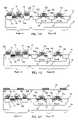
- FIGS. 1A to 1Fare cross-sectional views showing a production process of a solid-state imaging device according to Embodiment 1 of the present invention.
- FIGS. 2A to 2Fare cross-sectional views showing a production process of a solid-state imaging device according to Embodiment 2 of the present invention.
- FIG. 3is a circuit diagram schematically showing a configuration of a solid-state imaging device using an active pixel MOS sensor.
- FIG. 4is a cross-sectional view showing a conventional solid-state imaging device.
- the heat treatment processmay be provided at least after the formation of the photodiodes; after implantation of source and drains; and after implantation of substrate contact.
- the heat treatment processmay be performed using a furnace.
- the heat treatment process using the furnaceis performed at a temperature ranging from 850° C. to 900° C., inclusive, and for a time period of up to 60 minutes.
- the heat treatment process after the formation of gates of the MOS transistorsmay include an annealing step at a temperature that does not exceed 900° C. and for 15 minutes or longer.
- the plurality of MOS transistorsare constituted with N-type transistors only.
- region Ashows a pixel region of a solid-state imaging device and region B shows a peripheral circuit region.
- a production method according to Embodiment 1is favorably used for the case where a fine CMOS logic technology of 0.25 ⁇ m or finer is used, STI is used as element isolation and a gate oxide film of 10 nm or thinner is produced.
- a feature of this embodimentresides in that RTA is not used for activation annealing.
- the production method of a solid-state imaging device according to the present embodimentwill be described below, with reference to FIGS. 1A to 1F showing the production process in cross section.
- an element isolation region 21 with a STI structureis formed in a P-type silicon substrate 20 using a well-known technology.
- a signal storing region 25 of a photodiodeis formed in region A of the silicon substrate 20 .
- a N-well 26is formed in a P-MOS transistor formation region in region B, and a P-well 27 is formed in a N-MOS transistor formation region in region B.
- Typical dopantsare phosphorus for the N-well and boron for the P-well.
- a silicon oxide filmis formed as a gate insulation film 22 .
- a N-type drain region 24 ais formed at a portion adjacent to the read-out gate electrode 23 a in region A and a N-type LDD (Lightly Doped Drain) region 24 c is formed in a source/drain region of a N-MOS transistor in region B, which are formed by photolithography and an ion implantation method.
- a P-type LDD region 24 bis formed in a source/drain region of a P-MOS transistor.
- a silicon nitride film 28is formed to have a film thickness of 30 nm, for example, which is formed on the entire surface using an atmospheric pressure CVD (Chemical Vapor Deposition) method or the like. Furthermore, a silicon oxide film 29 is formed on the silicon nitride film 28 to have a film thickness of 85 nm using a low pressure CVD method or the like. After that, a photoresist film 30 is formed selectively on the silicon oxide film 29 at a region above the photodiode using a photolithography method.
- CVDChemical Vapor Deposition
- the silicon nitride film 28 and the silicon oxide film 29are dry-etched using a RIE (Reactive Ion Etching) technique where the photoresist film 30 serves as a mask.
- RIEReactive Ion Etching
- a gate side-wall insulation film 32is formed on the side walls of the gate electrodes 23 a , 23 b and 23 c , and a silicide block layer 31 is formed over the signal storing region 25 of the photodiode.
- the photoresist film 30is removed.
- the polycideis exposed by the dry-etching, this would be a contamination source of W (tungsten) as well as a cause of abnormal oxidation of the surface. Therefore, care should be taken not to expose the polycide.
- a P+type surface shield region 33is formed at the surface of the signal storing region 25 using a photolithography method and an ion implantation method. As a result, a P+NP type buried photodiode is formed.
- the surface shield region 33enables the shielding of a Si/SiO 2 interface located at the surface of the photodiode so as to prevent a depletion layer due to the signal storing region 25 from expanding to the Si/SiO 2 interface. Therefore, the surface shield region 33 can suppress the occurrence of a leakage current due to the Si/SiO 2 interface state.
- source/drain regions 34 a and 34 bare formed in the element regions.
- N+type ion implantationis performed for the formation of the source/drain region 34 a of the N-MOS region and P+type ion implantation is performed for the formation of the source/drain region 34 b of the P-MOS region.
- RTAactivation annealing is conducted with respect to ions implanted in the source/drain regions 34 a and 34 b .
- RTAis used for this step in a normal CMOS logic process
- the present embodimentdoes not use RTA because of the following reasons: the main reasons are three points including: RTA tends to induce crystal defects; RTA does not allow for the alleviation of stress applied to a photodiode from STI and gates; and since the P+type surface shield region 33 is an implantation layer with a considerably high density, a large number of defects may occur, and therefore insufficient annealing would lead to substantial growth of the defects, resulting in the occurrence of secondary defects.
- the activation annealingis conducted using furnace annealing, for example, instead of RTA.
- furnace annealinga sufficient heat treatment can be applied by setting a temperature at 850° C. and a time at 45 minutes, for example.
- the activation annealing to the P+type surface shield region 33is conducted after the formation of the shield region 33 .
- these processescan be conducted at one time.
- a pre-amorphization ion implantationis conducted.
- This pre-amorphization ion implantationis conducted in such a manner that As ions are used under the conditions of an acceleration voltage of 20 KeV and a dose of 3.0E14/cm 2 , for example.
- a Ti film(not illustrated) having a film thickness of 40 nm, for example, is formed as a silicide metal film on the entire surface using a sputtering method or the like.
- the silicide metalis not limited to Ti, and refractory metals such as Co, Ni and W may be used.
- RTPRapid Thermal Processing
- silicon in the silicon substrate 20 and Ti in the silicide metal filmreact at a region where the element regions of the silicon substrate 20 and the silicide metal film directly contact, so that the metal becomes silicide to form a Ti silicide (TiSi) film 35 .
- unreacted silicide metal filmis removed using a H 2 SO 4 or a HCl+H 2 O 2 solution, and moreover a RTP heat treatment is performed at a temperature at 850° C. for 10 seconds, for example.
- the Ti silicide (TiSi) film 35can be formed at regions that are not covered with the silicide block layer 31 .
- an interlayer insulation film 36is formed on the entire surface, followed by the planarization of this interlayer insulation film 36 by a CMP (Chemical Mechanical Polish) technology.
- Al wirings 37are formed selectively thereon, which serve as signal lines and connecting wirings in region A and connecting wirings in region B. Explanations of the later process for forming a multilayered wiring, which follows known techniques, are omitted.
- a feature of a production method of a solid-state imaging device according to Embodiment 2resides in that the process of Embodiment 1 is applied to a production process of a solid-state imaging device in which all of the transistors are configured with N-channel transistors (See JP 2002-270808 A, for example).
- the followingdescribes the present embodiment, with reference to FIGS. 2A to 2F showing the production process in cross section.
- the same steps as in Embodiment 1are simplified for their explanations, and different steps are explained in detail.
- an element isolation region 21 with a STI structureis formed selectively in a P-type silicon substrate 20 using a well-known technology.
- a signal storing region 25 of a photodiodeis formed in region A of the silicon substrate 20 .
- a P-well 27is formed in a N-MOS transistor formation region in region B.
- a silicon oxide filmis formed as a gate insulation film 22 .
- a N-type drain region 24 ais formed at a surface of the silicon substrate 20 at a portion adjacent to the read-out gate electrode 23 a in region A and a N-type LDD (Lightly Doped Drain) region 24 c is formed in a source/drain region of a N-MOS transistor in region B, which are formed by photolithography and an ion implantation method.
- a N-type LDD (Lightly Doped Drain) region 24 cis formed in a source/drain region of a N-MOS transistor in region B, which are formed by photolithography and an ion implantation method.
- a silicon nitride film 28is formed to have a film thickness of 30 nm, for example, which is formed on the entire surface using an atmospheric pressure CVD (Chemical Vapor Deposition) method or the like. Furthermore, a silicon oxide film 29 is formed on the silicon nitride film 28 to have a film thickness of 85 nm using a low pressure CVD method or the like. After that, a photoresist film 30 is formed on the silicon oxide film 29 at a region above the photodiode using a photolithography method.
- CVDChemical Vapor Deposition
- the silicon nitride film 28 and the silicon oxide film 29are dry-etched using a RIE (Reactive Ion Etching) technique where the photoresist film 30 serve as a mask.
- RIEReactive Ion Etching
- a gate side-wall insulation film 32is formed on the side walls of the gate electrodes 23 a , 23 b and 23 c , and a silicide block layer 31 is formed over the signal storing region 25 of the photodiode.
- the photoresist film 30is removed.
- the polycideis exposed by the dry-etching, this would be a contamination source of W (tungsten) as well as a cause of abnormal oxidation of the surface. Therefore, care should be taken not to expose the polycide.
- a P+type surface shield region 33is formed at the surface region of the signal storing region 25 of the photodiode in region A using a photolithography method and an ion implantation method. As a result, a P+NP type buried photodiode is formed.
- the surface shield region 33enables the shielding of a Si/SiO 2 interface located at the surface of the photodiode so as to prevent a depletion layer due to the signal storing region 25 from expanding to the Si/SiO 2 interface. Therefore, the surface shield region 33 can suppress the occurrence of a leakage current due to the Si/SiO 2 interface state.
- region BN+type ion implantation is performed for the formation of a source/drain region 34 b in the N-MOS region.
- activation annealingis conducted with respect to ions implanted in the source/drain region.
- RTAis not used for the activation annealing, and furnace annealing, for example, is used.
- furnace annealinga sufficient heat treatment can be applied by setting a temperature at 850° C. and a time at 45 minutes, for example.
- a pre-amorphization ion implantationis conducted.
- This pre-amorphization ion implantationis conducted in such a manner that As ions are used under the conditions of an acceleration voltage of 20 KeV and a dose of 3.0E 14/cm 2 , for example.
- a Ti film(not illustrated) having a film thickness of 40 nm, for example, is formed as a silicide metal film on the entire surface using a sputtering method or the like.
- the silicide metalis not limited to Ti, and refractory metals such as Co, Ni and W may be used.
- RTPis conducted in a nitrogen atmosphere at a temperature at 675° C. for 30 seconds, for example.
- silicon in the silicon substrate 20 and Ti in the silicide metal filmreact at a region where the element regions of the silicon substrate 20 and the silicide metal film directly contact, so that the metal becomes silicide to form a Ti silicide (TiSi) film 35 .
- unreacted silicide metal filmis removed using a H 2 SO 4 or a HCl+H 2 O 2 solution, and moreover a RTP heat treatment is performed under the conditions of a temperature at 850° C. for 10 seconds, for example.
- the Ti silicide (TiSi) film 35can be formed at regions that are not covered with the silicide block layer 31 .
- an interlayer insulation film 36is formed on the entire surface, followed by the planarization of this interlayer insulation film 36 by a CMP (Chemical Mechanical Polish) technology.
- Al wirings 37are formed selectively thereon, which serve as signal lines and connecting wirings in region A and connecting wirings in region B. Explanations of the later process for forming a multilayered wiring, which follows known techniques, are omitted.
- an optimum annealing technology for alleviating various stresses applied to a photodiode and for suppressing crystal defectscan be selected while suppressing the degradation of transistor characteristics of both of the P-MOS and N-MOS transistors, especially the degradation of a threshold voltage.
- polycideWSi/DPS
- doped polysiliconDPS
- implanted polysiliconmay be used.
- Ti silicideis used as the metal silicide
- Co, Ni or W silicidemay be used. Similar characteristics can be obtained from any one of these metals.
Landscapes
- Solid State Image Pick-Up Elements (AREA)
- Element Separation (AREA)
- Metal-Oxide And Bipolar Metal-Oxide Semiconductor Integrated Circuits (AREA)
- Insulated Gate Type Field-Effect Transistor (AREA)
Abstract
Description
- (1) Since the MOS-type solid-state imaging device is produced by a method in which a photodiode formation process is added to a CMOS logic process, no specific measures for suppressing image defects (especially typified by white flaws) as one of the properties of a solid-state imaging device are taken.
- (2) The production process of the MOS-type solid-state imaging device is based on a CMOS logic process, and therefore this process is tuned so as to realize a favorable basic performance of N-type and P-type transistors. Therefore, if the production process such as a heat treatment is modified, the performance of transistors may deteriorate.
Claims (12)
Applications Claiming Priority (2)
| Application Number | Priority Date | Filing Date | Title |
|---|---|---|---|
| JP2004004538AJP3729826B2 (en) | 2004-01-09 | 2004-01-09 | Method for manufacturing solid-state imaging device |
| JP2004-004538 | 2004-01-09 |
Publications (2)
| Publication Number | Publication Date |
|---|---|
| US20050153469A1 US20050153469A1 (en) | 2005-07-14 |
| US7285482B2true US7285482B2 (en) | 2007-10-23 |
Family
ID=34587729
Family Applications (1)
| Application Number | Title | Priority Date | Filing Date |
|---|---|---|---|
| US11/029,842Expired - LifetimeUS7285482B2 (en) | 2004-01-09 | 2005-01-05 | Method for producing solid-state imaging device |
Country Status (6)
| Country | Link |
|---|---|
| US (1) | US7285482B2 (en) |
| EP (1) | EP1553632A3 (en) |
| JP (1) | JP3729826B2 (en) |
| KR (1) | KR100661331B1 (en) |
| CN (1) | CN100454564C (en) |
| TW (1) | TW200527602A (en) |
Cited By (18)
| Publication number | Priority date | Publication date | Assignee | Title |
|---|---|---|---|---|
| US20070063303A1 (en)* | 2005-09-22 | 2007-03-22 | Lim Keun H | CMOS image sensor and method for manufacturing the same |
| US20090057735A1 (en)* | 2007-08-30 | 2009-03-05 | Hyoun-Min Beak | Image sensor having reduced dark current |
| US20100133592A1 (en)* | 2007-08-09 | 2010-06-03 | Panasonic Corporation | Solid-state imaging device |
| US20110220971A1 (en)* | 2009-09-17 | 2011-09-15 | Sionyx, Inc. | Photosensitive imaging devices and associated methods |
| US20130221196A1 (en)* | 2012-02-29 | 2013-08-29 | Kabushiki Kaisha Toshiba | Image sensor and manufacturing method thereof |
| US8680591B2 (en) | 2009-09-17 | 2014-03-25 | Sionyx, Inc. | Photosensitive imaging devices and associated methods |
| US8692198B2 (en) | 2010-04-21 | 2014-04-08 | Sionyx, Inc. | Photosensitive imaging devices and associated methods |
| US9496308B2 (en) | 2011-06-09 | 2016-11-15 | Sionyx, Llc | Process module for increasing the response of backside illuminated photosensitive imagers and associated methods |
| US9673250B2 (en) | 2013-06-29 | 2017-06-06 | Sionyx, Llc | Shallow trench textured regions and associated methods |
| US9762830B2 (en) | 2013-02-15 | 2017-09-12 | Sionyx, Llc | High dynamic range CMOS image sensor having anti-blooming properties and associated methods |
| US9761739B2 (en) | 2010-06-18 | 2017-09-12 | Sionyx, Llc | High speed photosensitive devices and associated methods |
| US9905599B2 (en) | 2012-03-22 | 2018-02-27 | Sionyx, Llc | Pixel isolation elements, devices and associated methods |
| US9911781B2 (en) | 2009-09-17 | 2018-03-06 | Sionyx, Llc | Photosensitive imaging devices and associated methods |
| US9939251B2 (en) | 2013-03-15 | 2018-04-10 | Sionyx, Llc | Three dimensional imaging utilizing stacked imager devices and associated methods |
| US10244188B2 (en) | 2011-07-13 | 2019-03-26 | Sionyx, Llc | Biometric imaging devices and associated methods |
| US10361083B2 (en) | 2004-09-24 | 2019-07-23 | President And Fellows Of Harvard College | Femtosecond laser-induced formation of submicrometer spikes on a semiconductor substrate |
| US10361232B2 (en) | 2009-09-17 | 2019-07-23 | Sionyx, Llc | Photosensitive imaging devices and associated methods |
| US10374109B2 (en) | 2001-05-25 | 2019-08-06 | President And Fellows Of Harvard College | Silicon-based visible and near-infrared optoelectric devices |
Families Citing this family (19)
| Publication number | Priority date | Publication date | Assignee | Title |
|---|---|---|---|---|
| JP4843951B2 (en)* | 2005-01-27 | 2011-12-21 | ソニー株式会社 | Solid-state imaging device manufacturing method, solid-state imaging device, and camera |
| KR100698100B1 (en)* | 2005-09-21 | 2007-03-23 | 동부일렉트로닉스 주식회사 | CMOS image sensor and its manufacturing method |
| JP2007142035A (en)* | 2005-11-16 | 2007-06-07 | Matsushita Electric Ind Co Ltd | Solid-state imaging device and manufacturing method thereof |
| US20070196988A1 (en)* | 2006-02-23 | 2007-08-23 | Shroff Mehul D | Poly pre-doping anneals for improved gate profiles |
| JP5116264B2 (en)* | 2006-07-10 | 2013-01-09 | キヤノン株式会社 | Photoelectric conversion device, method for manufacturing photoelectric conversion device, and imaging system using photoelectric conversion device |
| JP5110820B2 (en)* | 2006-08-02 | 2012-12-26 | キヤノン株式会社 | Photoelectric conversion device, photoelectric conversion device manufacturing method, and imaging system |
| US7732844B2 (en) | 2006-11-03 | 2010-06-08 | Taiwan Semiconductor Manufacturing Company, Ltd. | Crosstalk improvement through P on N structure for image sensor |
| KR100859481B1 (en)* | 2006-12-29 | 2008-09-23 | 동부일렉트로닉스 주식회사 | CMOS image sensor and its manufacturing method |
| US7679083B2 (en) | 2007-03-30 | 2010-03-16 | Samsung Electronics Co., Ltd. | Semiconductor integrated test structures for electron beam inspection of semiconductor wafers |
| JP5347283B2 (en)* | 2008-03-05 | 2013-11-20 | ソニー株式会社 | Solid-state imaging device and manufacturing method thereof |
| JP4793402B2 (en)* | 2008-04-21 | 2011-10-12 | ソニー株式会社 | Solid-state imaging device, manufacturing method thereof, and electronic apparatus |
| JP4759590B2 (en)* | 2008-05-09 | 2011-08-31 | キヤノン株式会社 | Photoelectric conversion device and imaging system using the same |
| JP5365221B2 (en)* | 2009-01-29 | 2013-12-11 | ソニー株式会社 | Solid-state imaging device, manufacturing method thereof, and imaging device |
| JP2012084748A (en)* | 2010-10-13 | 2012-04-26 | Sharp Corp | Solid state image sensor and electronic information apparatus |
| US20140273525A1 (en)* | 2013-03-13 | 2014-09-18 | Intermolecular, Inc. | Atomic Layer Deposition of Reduced-Leakage Post-Transition Metal Oxide Films |
| CN105336752B (en)* | 2014-06-23 | 2018-08-21 | 上海箩箕技术有限公司 | Area array sensor device and forming method thereof |
| JP6598830B2 (en)* | 2017-08-31 | 2019-10-30 | キヤノン株式会社 | Method for manufacturing photoelectric conversion device |
| CN118507500A (en)* | 2017-12-13 | 2024-08-16 | 松下知识产权经营株式会社 | Image pickup apparatus |
| CN108063146A (en)* | 2017-12-15 | 2018-05-22 | 上海华力微电子有限公司 | The manufacturing method of cmos image sensor |
Citations (8)
| Publication number | Priority date | Publication date | Assignee | Title |
|---|---|---|---|---|
| JP2000013370A (en) | 1998-06-19 | 2000-01-14 | Nippon Telegr & Teleph Corp <Ntt> | Multistage authentication method and apparatus, and recording medium recording this method |
| JP2001345439A (en) | 2000-03-28 | 2001-12-14 | Toshiba Corp | Solid-state imaging device and manufacturing method thereof |
| US6441444B1 (en) | 1998-10-22 | 2002-08-27 | Mitsubishi Denki Kabushiki Kaisha | Semiconductor device having a nitride barrier for preventing formation of structural defects |
| JP2002270808A (en) | 2001-03-13 | 2002-09-20 | Matsushita Electric Ind Co Ltd | MOS type imaging device |
| JP2002305296A (en) | 2001-04-09 | 2002-10-18 | Semiconductor Energy Lab Co Ltd | Semiconductor device and manufacturing method thereof |
| JP2003264277A (en) | 2002-03-07 | 2003-09-19 | Fujitsu Ltd | CMOS image sensor and method of manufacturing the same |
| US6855641B2 (en)* | 2002-04-25 | 2005-02-15 | Samsung Electronics Co., Ltd. | CMOS transistor having different PMOS and NMOS gate electrode structures and method of fabrication thereof |
| US20050164440A1 (en)* | 2003-03-31 | 2005-07-28 | Taiwan Semiconductor Manufacturing Co., Ltd. | Salicided MOS device and one-sided salicided MOS device, and simultaneous fabrication method thereof |
Family Cites Families (2)
| Publication number | Priority date | Publication date | Assignee | Title |
|---|---|---|---|---|
| US6194258B1 (en)* | 2000-01-18 | 2001-02-27 | Taiwan Semiconductor Manufacturing Company | Method of forming an image sensor cell and a CMOS logic circuit device |
| US6407440B1 (en)* | 2000-02-25 | 2002-06-18 | Micron Technology Inc. | Pixel cell with high storage capacitance for a CMOS imager |
- 2004
- 2004-01-09JPJP2004004538Apatent/JP3729826B2/ennot_activeExpired - Fee Related
- 2004-12-29KRKR1020040115125Apatent/KR100661331B1/ennot_activeExpired - Fee Related
- 2004-12-30TWTW093141288Apatent/TW200527602A/enunknown
- 2005
- 2005-01-05USUS11/029,842patent/US7285482B2/ennot_activeExpired - Lifetime
- 2005-01-10CNCNB2005100039036Apatent/CN100454564C/ennot_activeExpired - Fee Related
- 2005-01-10EPEP05000337Apatent/EP1553632A3/ennot_activeWithdrawn
Patent Citations (11)
| Publication number | Priority date | Publication date | Assignee | Title |
|---|---|---|---|---|
| JP2000013370A (en) | 1998-06-19 | 2000-01-14 | Nippon Telegr & Teleph Corp <Ntt> | Multistage authentication method and apparatus, and recording medium recording this method |
| US6441444B1 (en) | 1998-10-22 | 2002-08-27 | Mitsubishi Denki Kabushiki Kaisha | Semiconductor device having a nitride barrier for preventing formation of structural defects |
| JP2001345439A (en) | 2000-03-28 | 2001-12-14 | Toshiba Corp | Solid-state imaging device and manufacturing method thereof |
| US6570222B2 (en)* | 2000-03-28 | 2003-05-27 | Kabushiki Kaisha Toshiba | Solid state imaging device having a photodiode and a MOSFET |
| JP2002270808A (en) | 2001-03-13 | 2002-09-20 | Matsushita Electric Ind Co Ltd | MOS type imaging device |
| JP2002305296A (en) | 2001-04-09 | 2002-10-18 | Semiconductor Energy Lab Co Ltd | Semiconductor device and manufacturing method thereof |
| US6692984B2 (en) | 2001-04-09 | 2004-02-17 | Semiconductor Energy Laboratory Co., Ltd. | Method of manufacturing a semiconductor device |
| JP2003264277A (en) | 2002-03-07 | 2003-09-19 | Fujitsu Ltd | CMOS image sensor and method of manufacturing the same |
| US20030197228A1 (en) | 2002-03-07 | 2003-10-23 | Fujitsu Limited | CMOS image sensor and method of fabricating the same |
| US6855641B2 (en)* | 2002-04-25 | 2005-02-15 | Samsung Electronics Co., Ltd. | CMOS transistor having different PMOS and NMOS gate electrode structures and method of fabrication thereof |
| US20050164440A1 (en)* | 2003-03-31 | 2005-07-28 | Taiwan Semiconductor Manufacturing Co., Ltd. | Salicided MOS device and one-sided salicided MOS device, and simultaneous fabrication method thereof |
Cited By (31)
| Publication number | Priority date | Publication date | Assignee | Title |
|---|---|---|---|---|
| US10374109B2 (en) | 2001-05-25 | 2019-08-06 | President And Fellows Of Harvard College | Silicon-based visible and near-infrared optoelectric devices |
| US10741399B2 (en) | 2004-09-24 | 2020-08-11 | President And Fellows Of Harvard College | Femtosecond laser-induced formation of submicrometer spikes on a semiconductor substrate |
| US10361083B2 (en) | 2004-09-24 | 2019-07-23 | President And Fellows Of Harvard College | Femtosecond laser-induced formation of submicrometer spikes on a semiconductor substrate |
| US20070063303A1 (en)* | 2005-09-22 | 2007-03-22 | Lim Keun H | CMOS image sensor and method for manufacturing the same |
| US20100133592A1 (en)* | 2007-08-09 | 2010-06-03 | Panasonic Corporation | Solid-state imaging device |
| US8035178B2 (en) | 2007-08-09 | 2011-10-11 | Panasonic Corporation | Solid-state imaging device |
| US7955888B2 (en)* | 2007-08-30 | 2011-06-07 | Samsung Electronics Co., Ltd. | Method of fabricating image sensor having reduced dark current |
| US20090057735A1 (en)* | 2007-08-30 | 2009-03-05 | Hyoun-Min Beak | Image sensor having reduced dark current |
| US8476681B2 (en) | 2009-09-17 | 2013-07-02 | Sionyx, Inc. | Photosensitive imaging devices and associated methods |
| US8680591B2 (en) | 2009-09-17 | 2014-03-25 | Sionyx, Inc. | Photosensitive imaging devices and associated methods |
| US20110220971A1 (en)* | 2009-09-17 | 2011-09-15 | Sionyx, Inc. | Photosensitive imaging devices and associated methods |
| US10361232B2 (en) | 2009-09-17 | 2019-07-23 | Sionyx, Llc | Photosensitive imaging devices and associated methods |
| US9911781B2 (en) | 2009-09-17 | 2018-03-06 | Sionyx, Llc | Photosensitive imaging devices and associated methods |
| US10229951B2 (en) | 2010-04-21 | 2019-03-12 | Sionyx, Llc | Photosensitive imaging devices and associated methods |
| US8692198B2 (en) | 2010-04-21 | 2014-04-08 | Sionyx, Inc. | Photosensitive imaging devices and associated methods |
| US9741761B2 (en) | 2010-04-21 | 2017-08-22 | Sionyx, Llc | Photosensitive imaging devices and associated methods |
| US10505054B2 (en) | 2010-06-18 | 2019-12-10 | Sionyx, Llc | High speed photosensitive devices and associated methods |
| US9761739B2 (en) | 2010-06-18 | 2017-09-12 | Sionyx, Llc | High speed photosensitive devices and associated methods |
| US9496308B2 (en) | 2011-06-09 | 2016-11-15 | Sionyx, Llc | Process module for increasing the response of backside illuminated photosensitive imagers and associated methods |
| US10269861B2 (en) | 2011-06-09 | 2019-04-23 | Sionyx, Llc | Process module for increasing the response of backside illuminated photosensitive imagers and associated methods |
| US9666636B2 (en) | 2011-06-09 | 2017-05-30 | Sionyx, Llc | Process module for increasing the response of backside illuminated photosensitive imagers and associated methods |
| US10244188B2 (en) | 2011-07-13 | 2019-03-26 | Sionyx, Llc | Biometric imaging devices and associated methods |
| US9281328B2 (en)* | 2012-02-29 | 2016-03-08 | Kabushiki Kaisha Toshiba | Image sensor that includes a boundary region formed between a logic circuit region and an image-sensing element region and manufacturing method thereof |
| US20130221196A1 (en)* | 2012-02-29 | 2013-08-29 | Kabushiki Kaisha Toshiba | Image sensor and manufacturing method thereof |
| US10224359B2 (en) | 2012-03-22 | 2019-03-05 | Sionyx, Llc | Pixel isolation elements, devices and associated methods |
| US9905599B2 (en) | 2012-03-22 | 2018-02-27 | Sionyx, Llc | Pixel isolation elements, devices and associated methods |
| US9762830B2 (en) | 2013-02-15 | 2017-09-12 | Sionyx, Llc | High dynamic range CMOS image sensor having anti-blooming properties and associated methods |
| US9939251B2 (en) | 2013-03-15 | 2018-04-10 | Sionyx, Llc | Three dimensional imaging utilizing stacked imager devices and associated methods |
| US10347682B2 (en) | 2013-06-29 | 2019-07-09 | Sionyx, Llc | Shallow trench textured regions and associated methods |
| US9673250B2 (en) | 2013-06-29 | 2017-06-06 | Sionyx, Llc | Shallow trench textured regions and associated methods |
| US11069737B2 (en) | 2013-06-29 | 2021-07-20 | Sionyx, Llc | Shallow trench textured regions and associated methods |
Also Published As
| Publication number | Publication date |
|---|---|
| EP1553632A2 (en) | 2005-07-13 |
| CN100454564C (en) | 2009-01-21 |
| JP2005197605A (en) | 2005-07-21 |
| JP3729826B2 (en) | 2005-12-21 |
| CN1638140A (en) | 2005-07-13 |
| TW200527602A (en) | 2005-08-16 |
| EP1553632A3 (en) | 2009-06-03 |
| KR100661331B1 (en) | 2006-12-27 |
| KR20050073530A (en) | 2005-07-14 |
| US20050153469A1 (en) | 2005-07-14 |
Similar Documents
| Publication | Publication Date | Title |
|---|---|---|
| US7285482B2 (en) | Method for producing solid-state imaging device | |
| JP5320659B2 (en) | Solid-state imaging device | |
| JP5426114B2 (en) | Semiconductor device and manufacturing method thereof | |
| US8907375B2 (en) | Method of manufacturing semiconductor device, solid-state imaging device, and solid-state imaging apparatus | |
| US8501520B2 (en) | Manufacturing method for a solid-state image sensor | |
| US7595210B2 (en) | Method of manufacturing complementary metal oxide semiconductor image sensor | |
| CN101366114A (en) | Method and apparatus for providing integrated circuits with P- and N-doped gates | |
| JP2007027705A (en) | Image sensor and manufacturing method thereof | |
| JP4729933B2 (en) | Method for manufacturing solid-state imaging device | |
| JP4449106B2 (en) | MOS type solid-state imaging device and manufacturing method thereof | |
| US6492668B2 (en) | Solid imaging device and production method thereof | |
| JP2011155168A (en) | Semiconductor device, method for manufacturing the same, and solid-state imaging device | |
| CN105575986A (en) | Solid-state imaging device and method of manufacturing solid-state imaging device | |
| JP2000012823A (en) | Solid-state imaging device and method of manufacturing the same | |
| JP2008016723A (en) | Solid-state imaging device manufacturing method and solid-state imaging device | |
| JP2008177306A (en) | Solid-state imaging device | |
| JP2005223085A (en) | Semiconductor device and manufacturing method therefor | |
| JP2008108916A (en) | Solid-state imaging apparatus, and electronic equipment | |
| US7659133B2 (en) | Method for manufacturing CMOS image sensor | |
| JP2009123865A (en) | Solid-state imaging device and manufacturing method thereof | |
| JP2005302836A (en) | Method for manufacturing solid-state imaging device | |
| JP4810831B2 (en) | Semiconductor device and manufacturing method thereof | |
| JP2009038207A (en) | Solid-state imaging device and manufacturing method thereof | |
| JP2006261414A (en) | Solid-state imaging device and manufacturing method thereof | |
| JP2006294756A (en) | Manufacturing method of semiconductor device |
Legal Events
| Date | Code | Title | Description |
|---|---|---|---|
| AS | Assignment | Owner name:MATSUSHITA ELECTRIC INDUSTRIAL CO., LTD., JAPAN Free format text:ASSIGNMENT OF ASSIGNORS INTEREST;ASSIGNOR:OCHI, MOTOTAKA;REEL/FRAME:016158/0532 Effective date:20041220 | |
| STCF | Information on status: patent grant | Free format text:PATENTED CASE | |
| FEPP | Fee payment procedure | Free format text:PAYOR NUMBER ASSIGNED (ORIGINAL EVENT CODE: ASPN); ENTITY STATUS OF PATENT OWNER: LARGE ENTITY | |
| FPAY | Fee payment | Year of fee payment:4 | |
| AS | Assignment | Owner name:PANASONIC CORPORATION, JAPAN Free format text:CHANGE OF NAME;ASSIGNOR:MATSUSHITA ELECTRIC INDUSTRIAL CO., LTD.;REEL/FRAME:031947/0358 Effective date:20081001 | |
| AS | Assignment | Owner name:PANASONIC CORPORATION, JAPAN Free format text:LIEN;ASSIGNOR:COLLABO INNOVATIONS, INC.;REEL/FRAME:031997/0445 Effective date:20131213 | |
| AS | Assignment | Owner name:COLLABO INNOVATIONS, INC., CANADA Free format text:ASSIGNMENT OF ASSIGNORS INTEREST;ASSIGNOR:PANASONIC CORPORATION;REEL/FRAME:033021/0806 Effective date:20131212 | |
| FPAY | Fee payment | Year of fee payment:8 | |
| MAFP | Maintenance fee payment | Free format text:PAYMENT OF MAINTENANCE FEE, 12TH YEAR, LARGE ENTITY (ORIGINAL EVENT CODE: M1553); ENTITY STATUS OF PATENT OWNER: LARGE ENTITY Year of fee payment:12 |