US7285308B2 - Chemical vapor deposition of high conductivity, adherent thin films of ruthenium - Google Patents
Chemical vapor deposition of high conductivity, adherent thin films of rutheniumDownload PDFInfo
- Publication number
- US7285308B2 US7285308B2US10/803,750US80375004AUS7285308B2US 7285308 B2US7285308 B2US 7285308B2US 80375004 AUS80375004 AUS 80375004AUS 7285308 B2US7285308 B2US 7285308B2
- Authority
- US
- United States
- Prior art keywords
- ruthenium
- range
- precursor
- deposition
- nucleation layer
- Prior art date
- Legal status (The legal status is an assumption and is not a legal conclusion. Google has not performed a legal analysis and makes no representation as to the accuracy of the status listed.)
- Expired - Lifetime, expires
Links
- 229910052707rutheniumInorganic materials0.000titleclaimsabstractdescription220
- KJTLSVCANCCWHF-UHFFFAOYSA-NRutheniumChemical compound[Ru]KJTLSVCANCCWHF-UHFFFAOYSA-N0.000titleclaimsabstractdescription214
- 238000005229chemical vapour depositionMethods0.000titleclaimsabstractdescription61
- 239000010409thin filmSubstances0.000titleclaimsabstractdescription53
- 230000001464adherent effectEffects0.000titledescription6
- 238000000034methodMethods0.000claimsabstractdescription181
- 238000000151depositionMethods0.000claimsabstractdescription142
- 230000008021depositionEffects0.000claimsabstractdescription119
- 230000006911nucleationEffects0.000claimsabstractdescription75
- 238000010899nucleationMethods0.000claimsabstractdescription75
- 239000000758substrateSubstances0.000claimsabstractdescription59
- 239000002243precursorSubstances0.000claimsdescription103
- 239000010408filmSubstances0.000claimsdescription85
- 239000007789gasSubstances0.000claimsdescription76
- 239000000376reactantSubstances0.000claimsdescription43
- QVGXLLKOCUKJST-UHFFFAOYSA-Natomic oxygenChemical compound[O]QVGXLLKOCUKJST-UHFFFAOYSA-N0.000claimsdescription35
- 229910052760oxygenInorganic materials0.000claimsdescription35
- 239000001301oxygenSubstances0.000claimsdescription35
- 239000000203mixtureSubstances0.000claimsdescription34
- 238000006557surface reactionMethods0.000claimsdescription19
- 239000012535impuritySubstances0.000claimsdescription14
- 229910052739hydrogenInorganic materials0.000claimsdescription13
- 125000006527(C1-C5) alkyl groupChemical group0.000claimsdescription11
- 239000007787solidSubstances0.000claimsdescription11
- -1ruthenium halidesChemical class0.000claimsdescription10
- UFHFLCQGNIYNRP-UHFFFAOYSA-NHydrogenChemical compound[H][H]UFHFLCQGNIYNRP-UHFFFAOYSA-N0.000claimsdescription8
- 230000003635deoxygenating effectEffects0.000claimsdescription8
- 239000001257hydrogenSubstances0.000claimsdescription7
- 239000000463materialSubstances0.000claimsdescription7
- 229910001925ruthenium oxideInorganic materials0.000claimsdescription7
- 239000002904solventSubstances0.000claimsdescription7
- RYGMFSIKBFXOCR-UHFFFAOYSA-NCopperChemical compound[Cu]RYGMFSIKBFXOCR-UHFFFAOYSA-N0.000claimsdescription6
- VYPSYNLAJGMNEJ-UHFFFAOYSA-NSilicium dioxideChemical compoundO=[Si]=OVYPSYNLAJGMNEJ-UHFFFAOYSA-N0.000claimsdescription6
- 229910052802copperInorganic materials0.000claimsdescription6
- 239000010949copperSubstances0.000claimsdescription6
- 239000007788liquidSubstances0.000claimsdescription6
- WOCIAKWEIIZHES-UHFFFAOYSA-Nruthenium(iv) oxideChemical compoundO=[Ru]=OWOCIAKWEIIZHES-UHFFFAOYSA-N0.000claimsdescription6
- ROZSPJBPUVWBHW-UHFFFAOYSA-N[Ru]=OChemical class[Ru]=OROZSPJBPUVWBHW-UHFFFAOYSA-N0.000claimsdescription5
- 238000013459approachMethods0.000claimsdescription5
- 239000011261inert gasSubstances0.000claimsdescription5
- CURLTUGMZLYLDI-UHFFFAOYSA-NCarbon dioxideChemical compoundO=C=OCURLTUGMZLYLDI-UHFFFAOYSA-N0.000claimsdescription4
- GQPLMRYTRLFLPF-UHFFFAOYSA-NNitrous OxideChemical compound[O-][N+]#NGQPLMRYTRLFLPF-UHFFFAOYSA-N0.000claimsdescription4
- NRTOMJZYCJJWKI-UHFFFAOYSA-NTitanium nitrideChemical compound[Ti]#NNRTOMJZYCJJWKI-UHFFFAOYSA-N0.000claimsdescription4
- 238000000137annealingMethods0.000claimsdescription4
- 229910052454barium strontium titanateInorganic materials0.000claimsdescription4
- 239000003638chemical reducing agentSubstances0.000claimsdescription4
- 229910052451lead zirconate titanateInorganic materials0.000claimsdescription4
- BPUBBGLMJRNUCC-UHFFFAOYSA-Noxygen(2-);tantalum(5+)Chemical compound[O-2].[O-2].[O-2].[O-2].[O-2].[Ta+5].[Ta+5]BPUBBGLMJRNUCC-UHFFFAOYSA-N0.000claimsdescription4
- 229910052581Si3N4Inorganic materials0.000claimsdescription3
- XUIMIQQOPSSXEZ-UHFFFAOYSA-NSiliconChemical compound[Si]XUIMIQQOPSSXEZ-UHFFFAOYSA-N0.000claimsdescription3
- UQZIWOQVLUASCR-UHFFFAOYSA-Nalumane;titaniumChemical compound[AlH3].[Ti]UQZIWOQVLUASCR-UHFFFAOYSA-N0.000claimsdescription3
- 150000002431hydrogenChemical class0.000claimsdescription3
- HFGPZNIAWCZYJU-UHFFFAOYSA-Nlead zirconate titanateChemical compound[O-2].[O-2].[O-2].[O-2].[O-2].[Ti+4].[Zr+4].[Pb+2]HFGPZNIAWCZYJU-UHFFFAOYSA-N0.000claimsdescription3
- 230000001590oxidative effectEffects0.000claimsdescription3
- 229910052710siliconInorganic materials0.000claimsdescription3
- 239000010703siliconSubstances0.000claimsdescription3
- 235000012239silicon dioxideNutrition0.000claimsdescription3
- 239000000377silicon dioxideSubstances0.000claimsdescription3
- HQVNEWCFYHHQES-UHFFFAOYSA-Nsilicon nitrideChemical compoundN12[Si]34N5[Si]62N3[Si]51N64HQVNEWCFYHHQES-UHFFFAOYSA-N0.000claimsdescription3
- MZLGASXMSKOWSE-UHFFFAOYSA-Ntantalum nitrideChemical compound[Ta]#NMZLGASXMSKOWSE-UHFFFAOYSA-N0.000claimsdescription3
- UGFAIRIUMAVXCW-UHFFFAOYSA-NCarbon monoxideChemical compound[O+]#[C-]UGFAIRIUMAVXCW-UHFFFAOYSA-N0.000claimsdescription2
- CBENFWSGALASAD-UHFFFAOYSA-NOzoneChemical compound[O-][O+]=OCBENFWSGALASAD-UHFFFAOYSA-N0.000claimsdescription2
- 239000001569carbon dioxideSubstances0.000claimsdescription2
- 229910002092carbon dioxideInorganic materials0.000claimsdescription2
- 229910002091carbon monoxideInorganic materials0.000claimsdescription2
- 239000001272nitrous oxideSubstances0.000claimsdescription2
- 230000002123temporal effectEffects0.000claimsdescription2
- 239000007983Tris bufferSubstances0.000claims14
- 150000003303rutheniumChemical class0.000claims4
- FZHCFNGSGGGXEH-UHFFFAOYSA-NruthenoceneChemical compound[Ru+2].C=1C=C[CH-]C=1.C=1C=C[CH-]C=1FZHCFNGSGGGXEH-UHFFFAOYSA-N0.000claims3
- IYWJIYWFPADQAN-LNTINUHCSA-N(z)-4-hydroxypent-3-en-2-one;rutheniumChemical compound[Ru].C\C(O)=C\C(C)=O.C\C(O)=C\C(C)=O.C\C(O)=C\C(C)=OIYWJIYWFPADQAN-LNTINUHCSA-N0.000claims2
- CEPICIBPGDWCRU-UHFFFAOYSA-N[Si].[Hf]Chemical compound[Si].[Hf]CEPICIBPGDWCRU-UHFFFAOYSA-N0.000claims2
- ILCYGSITMBHYNK-UHFFFAOYSA-N[Si]=O.[Hf]Chemical compound[Si]=O.[Hf]ILCYGSITMBHYNK-UHFFFAOYSA-N0.000claims2
- 150000001875compoundsChemical class0.000claims2
- 238000006392deoxygenation reactionMethods0.000claims1
- 150000003304ruthenium compoundsChemical class0.000claims1
- 239000000243solutionSubstances0.000claims1
- 230000008569processEffects0.000description82
- WYURNTSHIVDZCO-UHFFFAOYSA-NTetrahydrofuranChemical compoundC1CCOC1WYURNTSHIVDZCO-UHFFFAOYSA-N0.000description12
- 230000006870functionEffects0.000description11
- 239000003990capacitorSubstances0.000description8
- 0[1*]c1c([2*])c([3*])c([4*])c1[5*]Chemical compound[1*]c1c([2*])c([3*])c([4*])c1[5*]0.000description7
- 229910052751metalInorganic materials0.000description7
- 239000002184metalSubstances0.000description7
- 125000001449isopropyl groupChemical group[H]C([H])([H])C([H])(*)C([H])([H])[H]0.000description6
- 125000004108n-butyl groupChemical group[H]C([H])([H])C([H])([H])C([H])([H])C([H])([H])*0.000description6
- 125000004123n-propyl groupChemical group[H]C([H])([H])C([H])([H])C([H])([H])*0.000description6
- 125000000999tert-butyl groupChemical group[H]C([H])([H])C(*)(C([H])([H])[H])C([H])([H])[H]0.000description6
- YLQBMQCUIZJEEH-UHFFFAOYSA-NtetrahydrofuranNatural productsC=1C=COC=1YLQBMQCUIZJEEH-UHFFFAOYSA-N0.000description6
- 238000002474experimental methodMethods0.000description5
- 239000012159carrier gasSubstances0.000description4
- 238000005137deposition processMethods0.000description4
- OKTJSMMVPCPJKN-UHFFFAOYSA-NCarbonChemical compound[C]OKTJSMMVPCPJKN-UHFFFAOYSA-N0.000description3
- 230000004888barrier functionEffects0.000description3
- 229910052799carbonInorganic materials0.000description3
- UOCJDOLVGGIYIQ-PBFPGSCMSA-NcefatrizineChemical groupS([C@@H]1[C@@H](C(N1C=1C(O)=O)=O)NC(=O)[C@H](N)C=2C=CC(O)=CC=2)CC=1CSC=1C=NNN=1UOCJDOLVGGIYIQ-PBFPGSCMSA-N0.000description3
- 230000010354integrationEffects0.000description3
- 238000004544sputter depositionMethods0.000description3
- RRKODOZNUZCUBN-CCAGOZQPSA-N(1z,3z)-cycloocta-1,3-dieneChemical compoundC1CC\C=C/C=C\C1RRKODOZNUZCUBN-CCAGOZQPSA-N0.000description2
- XNMQEEKYCVKGBD-UHFFFAOYSA-N2-butyneChemical compoundCC#CCXNMQEEKYCVKGBD-UHFFFAOYSA-N0.000description2
- XKRFYHLGVUSROY-UHFFFAOYSA-NArgonChemical compound[Ar]XKRFYHLGVUSROY-UHFFFAOYSA-N0.000description2
- IJGRMHOSHXDMSA-UHFFFAOYSA-NAtomic nitrogenChemical compoundN#NIJGRMHOSHXDMSA-UHFFFAOYSA-N0.000description2
- 229910019891RuCl3Inorganic materials0.000description2
- 150000001335aliphatic alkanesChemical class0.000description2
- 230000008859changeEffects0.000description2
- 239000013078crystalSubstances0.000description2
- 230000003247decreasing effectEffects0.000description2
- 230000009977dual effectEffects0.000description2
- 238000000572ellipsometryMethods0.000description2
- 229910052735hafniumInorganic materials0.000description2
- 229910000449hafnium oxideInorganic materials0.000description2
- 239000012705liquid precursorSubstances0.000description2
- 238000010926purgeMethods0.000description2
- YBCAZPLXEGKKFM-UHFFFAOYSA-Kruthenium(iii) chlorideChemical compound[Cl-].[Cl-].[Cl-].[Ru+3]YBCAZPLXEGKKFM-UHFFFAOYSA-K0.000description2
- PBCFLUZVCVVTBY-UHFFFAOYSA-Ntantalum pentoxideInorganic materialsO=[Ta](=O)O[Ta](=O)=OPBCFLUZVCVVTBY-UHFFFAOYSA-N0.000description2
- 230000008016vaporizationEffects0.000description2
- 238000009834vaporizationMethods0.000description2
- RYOGZVTWMZNTGL-UDRCNDPASA-N(1z,5z)-1,5-dimethylcycloocta-1,5-dieneChemical compoundC\C1=C\CC\C(C)=C/CC1RYOGZVTWMZNTGL-UDRCNDPASA-N0.000description1
- 125000004178(C1-C4) alkyl groupChemical group0.000description1
- MYMOFIZGZYHOMD-UHFFFAOYSA-NDioxygenChemical compoundO=OMYMOFIZGZYHOMD-UHFFFAOYSA-N0.000description1
- 239000002879Lewis baseSubstances0.000description1
- BPQQTUXANYXVAA-UHFFFAOYSA-NOrthosilicateChemical compound[O-][Si]([O-])([O-])[O-]BPQQTUXANYXVAA-UHFFFAOYSA-N0.000description1
- CUJRVFIICFDLGR-UHFFFAOYSA-NacetylacetonateChemical compoundCC(=O)[CH-]C(C)=OCUJRVFIICFDLGR-UHFFFAOYSA-N0.000description1
- 239000000853adhesiveSubstances0.000description1
- 230000001070adhesive effectEffects0.000description1
- 150000001336alkenesChemical class0.000description1
- 150000001345alkine derivativesChemical class0.000description1
- 239000003708ampulSubstances0.000description1
- 229910052786argonInorganic materials0.000description1
- 239000012298atmosphereSubstances0.000description1
- NQZFAUXPNWSLBI-UHFFFAOYSA-Ncarbon monoxide;rutheniumChemical compound[Ru].[Ru].[Ru].[O+]#[C-].[O+]#[C-].[O+]#[C-].[O+]#[C-].[O+]#[C-].[O+]#[C-].[O+]#[C-].[O+]#[C-].[O+]#[C-].[O+]#[C-].[O+]#[C-].[O+]#[C-]NQZFAUXPNWSLBI-UHFFFAOYSA-N0.000description1
- 230000015556catabolic processEffects0.000description1
- 238000006243chemical reactionMethods0.000description1
- 239000004020conductorSubstances0.000description1
- 238000010924continuous productionMethods0.000description1
- 150000001925cycloalkenesChemical class0.000description1
- 230000007547defectEffects0.000description1
- 230000002939deleterious effectEffects0.000description1
- 229910001882dioxygenInorganic materials0.000description1
- 239000007772electrode materialSubstances0.000description1
- 239000003623enhancerSubstances0.000description1
- 125000003709fluoroalkyl groupChemical group0.000description1
- VBJZVLUMGGDVMO-UHFFFAOYSA-Nhafnium atomChemical compound[Hf]VBJZVLUMGGDVMO-UHFFFAOYSA-N0.000description1
- WIHZLLGSGQNAGK-UHFFFAOYSA-Nhafnium(4+);oxygen(2-)Chemical compound[O-2].[O-2].[Hf+4]WIHZLLGSGQNAGK-UHFFFAOYSA-N0.000description1
- 238000010438heat treatmentMethods0.000description1
- 238000010348incorporationMethods0.000description1
- 150000002500ionsChemical class0.000description1
- 125000000959isobutyl groupChemical group[H]C([H])([H])C([H])(C([H])([H])[H])C([H])([H])*0.000description1
- 150000007527lewis basesChemical class0.000description1
- 238000004519manufacturing processMethods0.000description1
- 230000015654memoryEffects0.000description1
- 238000002488metal-organic chemical vapour depositionMethods0.000description1
- 230000007935neutral effectEffects0.000description1
- 229910052757nitrogenInorganic materials0.000description1
- 229910000510noble metalInorganic materials0.000description1
- 229910001927ruthenium tetroxideInorganic materials0.000description1
- 229920006395saturated elastomerPolymers0.000description1
- 239000004065semiconductorSubstances0.000description1
- 238000000391spectroscopic ellipsometryMethods0.000description1
- 239000000126substanceSubstances0.000description1
- 238000012360testing methodMethods0.000description1
- 238000000427thin-film depositionMethods0.000description1
- 238000012876topographyMethods0.000description1
- 239000006200vaporizerSubstances0.000description1
Images


Classifications
- C—CHEMISTRY; METALLURGY
- C23—COATING METALLIC MATERIAL; COATING MATERIAL WITH METALLIC MATERIAL; CHEMICAL SURFACE TREATMENT; DIFFUSION TREATMENT OF METALLIC MATERIAL; COATING BY VACUUM EVAPORATION, BY SPUTTERING, BY ION IMPLANTATION OR BY CHEMICAL VAPOUR DEPOSITION, IN GENERAL; INHIBITING CORROSION OF METALLIC MATERIAL OR INCRUSTATION IN GENERAL
- C23C—COATING METALLIC MATERIAL; COATING MATERIAL WITH METALLIC MATERIAL; SURFACE TREATMENT OF METALLIC MATERIAL BY DIFFUSION INTO THE SURFACE, BY CHEMICAL CONVERSION OR SUBSTITUTION; COATING BY VACUUM EVAPORATION, BY SPUTTERING, BY ION IMPLANTATION OR BY CHEMICAL VAPOUR DEPOSITION, IN GENERAL
- C23C16/00—Chemical coating by decomposition of gaseous compounds, without leaving reaction products of surface material in the coating, i.e. chemical vapour deposition [CVD] processes
- C23C16/44—Chemical coating by decomposition of gaseous compounds, without leaving reaction products of surface material in the coating, i.e. chemical vapour deposition [CVD] processes characterised by the method of coating
- C23C16/455—Chemical coating by decomposition of gaseous compounds, without leaving reaction products of surface material in the coating, i.e. chemical vapour deposition [CVD] processes characterised by the method of coating characterised by the method used for introducing gases into reaction chamber or for modifying gas flows in reaction chamber
- C23C16/45557—Pulsed pressure or control pressure
- C—CHEMISTRY; METALLURGY
- C23—COATING METALLIC MATERIAL; COATING MATERIAL WITH METALLIC MATERIAL; CHEMICAL SURFACE TREATMENT; DIFFUSION TREATMENT OF METALLIC MATERIAL; COATING BY VACUUM EVAPORATION, BY SPUTTERING, BY ION IMPLANTATION OR BY CHEMICAL VAPOUR DEPOSITION, IN GENERAL; INHIBITING CORROSION OF METALLIC MATERIAL OR INCRUSTATION IN GENERAL
- C23C—COATING METALLIC MATERIAL; COATING MATERIAL WITH METALLIC MATERIAL; SURFACE TREATMENT OF METALLIC MATERIAL BY DIFFUSION INTO THE SURFACE, BY CHEMICAL CONVERSION OR SUBSTITUTION; COATING BY VACUUM EVAPORATION, BY SPUTTERING, BY ION IMPLANTATION OR BY CHEMICAL VAPOUR DEPOSITION, IN GENERAL
- C23C16/00—Chemical coating by decomposition of gaseous compounds, without leaving reaction products of surface material in the coating, i.e. chemical vapour deposition [CVD] processes
- C23C16/02—Pretreatment of the material to be coated
- C23C16/0272—Deposition of sub-layers, e.g. to promote the adhesion of the main coating
- C—CHEMISTRY; METALLURGY
- C23—COATING METALLIC MATERIAL; COATING MATERIAL WITH METALLIC MATERIAL; CHEMICAL SURFACE TREATMENT; DIFFUSION TREATMENT OF METALLIC MATERIAL; COATING BY VACUUM EVAPORATION, BY SPUTTERING, BY ION IMPLANTATION OR BY CHEMICAL VAPOUR DEPOSITION, IN GENERAL; INHIBITING CORROSION OF METALLIC MATERIAL OR INCRUSTATION IN GENERAL
- C23C—COATING METALLIC MATERIAL; COATING MATERIAL WITH METALLIC MATERIAL; SURFACE TREATMENT OF METALLIC MATERIAL BY DIFFUSION INTO THE SURFACE, BY CHEMICAL CONVERSION OR SUBSTITUTION; COATING BY VACUUM EVAPORATION, BY SPUTTERING, BY ION IMPLANTATION OR BY CHEMICAL VAPOUR DEPOSITION, IN GENERAL
- C23C16/00—Chemical coating by decomposition of gaseous compounds, without leaving reaction products of surface material in the coating, i.e. chemical vapour deposition [CVD] processes
- C23C16/06—Chemical coating by decomposition of gaseous compounds, without leaving reaction products of surface material in the coating, i.e. chemical vapour deposition [CVD] processes characterised by the deposition of metallic material
- C23C16/16—Chemical coating by decomposition of gaseous compounds, without leaving reaction products of surface material in the coating, i.e. chemical vapour deposition [CVD] processes characterised by the deposition of metallic material from metal carbonyl compounds
- C—CHEMISTRY; METALLURGY
- C23—COATING METALLIC MATERIAL; COATING MATERIAL WITH METALLIC MATERIAL; CHEMICAL SURFACE TREATMENT; DIFFUSION TREATMENT OF METALLIC MATERIAL; COATING BY VACUUM EVAPORATION, BY SPUTTERING, BY ION IMPLANTATION OR BY CHEMICAL VAPOUR DEPOSITION, IN GENERAL; INHIBITING CORROSION OF METALLIC MATERIAL OR INCRUSTATION IN GENERAL
- C23C—COATING METALLIC MATERIAL; COATING MATERIAL WITH METALLIC MATERIAL; SURFACE TREATMENT OF METALLIC MATERIAL BY DIFFUSION INTO THE SURFACE, BY CHEMICAL CONVERSION OR SUBSTITUTION; COATING BY VACUUM EVAPORATION, BY SPUTTERING, BY ION IMPLANTATION OR BY CHEMICAL VAPOUR DEPOSITION, IN GENERAL
- C23C16/00—Chemical coating by decomposition of gaseous compounds, without leaving reaction products of surface material in the coating, i.e. chemical vapour deposition [CVD] processes
- C23C16/06—Chemical coating by decomposition of gaseous compounds, without leaving reaction products of surface material in the coating, i.e. chemical vapour deposition [CVD] processes characterised by the deposition of metallic material
- C23C16/18—Chemical coating by decomposition of gaseous compounds, without leaving reaction products of surface material in the coating, i.e. chemical vapour deposition [CVD] processes characterised by the deposition of metallic material from metallo-organic compounds
Definitions
- the present inventionrelates to the chemical vapor deposition of ruthenium thin films. More specifically, the present invention relates to a multi-step process for the chemical vapor deposition of ruthenium thin films, including the deposition of a ruthenium nucleation layer that provides superior adhesion to, and continuous coverage of, the substrate followed by the deposition of a highly conductive ruthenium upper layer that is adherent to the nucleation layer.
- the noble metal ruthenium (Ru)is being widely investigated for use in conductive layers of integrated circuits (IC).
- layers comprising rutheniumare being investigated for use as the lower (bottom) electrode of IC capacitors that may be used, for example, in Dynamic Random Access Memories (DRAM).
- DRAMDynamic Random Access Memories
- ruthenium thin filmsare used as the high work function gate electrode material for dual metal gates and as a direct-platable barrier material for Cu-low k dual damascene interconnects.
- the major challenges in depositing ruthenium filmsinclude obtaining a ruthenium thin film that is highly conductive, i.e., having low resistance, while displaying good adhesion to the substrate, e.g., dielectric, surface and high conformality.
- the deposition of very thin ruthenium films ( ⁇ 10 nm) that are smooth and continuoushas been challenging.
- sputtering methodshave been used to deposit ruthenium films, yielding layers having good surface morphology and low resistance.
- sputteringis limited by poor step coverage when the critical dimensions (CD) are small and the aspect ratios are high, which may be disadvantageous when forming three-dimensional high capacitance electrode structures such as cylinder-type or fin-shaped capacitor electrodes or when producing direct-platable barriers on high aspect ratio structures, e.g., copper interconnects.
- CDcritical dimensions
- sputtered rutheniumhas been shown to possess the necessary work function for p-MOS transistors, the potential for ion damage to the transistor channel precludes the consideration of sputtering for mass production.
- Chemical vapor depositionis also used to form ruthenium layers.
- rutheniumis deposited on an IC substrate, e.g., a dielectric layer, using a gasified ruthenium source and a co-reactant gas.
- CVD of thin ruthenium filmsachieves good step coverage and wafer-to-wafer repeatability on complicated topography.
- a ruthenium layer formed by CVDmay have poor surface morphology or high impurity content and as such, a high electrical resistivity. If the ruthenium layer is the bottom electrode of a MIM capacitor, poor surface morphology can result in high leakage current in the capacitor.
- a titanium nitride (TiN) sticking layermay be deposited onto a substrate followed by deposition of the ruthenium electrode on the sticking layer.
- TiNtitanium nitride
- the sticking layer producedis often too thick for increasingly fine feature sizes, and as such has limited applicability, or alternatively the sticking layer modifies the effective work function of the metal.
- U.S. Pat. No. 6,479,100 to Jin et al.discloses a method of depositing a ruthenium seed layer on a substrate using CVD.
- the deposited ruthenium seed layersshould contain oxygen to improve adherence to the substrate, but the characteristics of the subsequently deposited thin ruthenium film onto the seed layer were enhanced when the oxygen content of the seed layer is relatively low.
- Jin et al.disclosed that the deposited ruthenium oxide seed layer must be annealed prior to deposition of the pure ruthenium thin metal film thereon.
- the reported resistivity of the deposited thin filmswas 50 to 55 ⁇ -cm for 130 to 140 ⁇ films, which is a factor of seven worse than the resistivity for bulk ruthenium (7.4 ⁇ -cm) and is worse than the resistivity for bulk RuO 2 (44 ⁇ -cm).
- the present inventionrelates to the chemical vapor deposition of ruthenium thin films. More specifically, the present invention relates to a multi-step process for the chemical vapor deposition of ruthenium thin films, including the deposition of a ruthenium nucleation layer that provides superior adhesion to, and continuous coverage of, the substrate followed by the deposition of a highly conductive ruthenium upper layer that is adherent to the nucleation layer.
- the inventionrelates to a method for depositing a ruthenium thin film onto a substrate, said method comprising:
- the inventionrelates to a method for depositing a ruthenium thin film onto a substrate, said method comprising:
- FIG. 1is a schematic of the process conditions as a function of time (arbitrary units) associated with deposition process 7 .
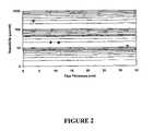
- FIG. 2illustrates the resistivity of films as a function of film thickness for ruthenium thin films deposited according to CVD process 7 described herein.
- FIG. 3is a schematic of process variables as a function of time (arbitrary units) for the pulsed process described in Example 5.
- FIG. 4is a plot of the resistivity of the films as a function of film thickness.
- the present inventionrelates to multi-step methods for depositing ruthenium thin films having high conductivity and superior adherence to the substrate.
- the methodincludes the deposition of a ruthenium nucleation layer under conditions that provide superior adhesion to, and continuous coverage of, the substrate surface followed by the deposition of a highly conductive ruthenium upper layer that is adherent to the nucleation layer. Both layers are deposited using chemical vapor deposition (CVD).
- CVDchemical vapor deposition
- peel-resistant layer filmsare films deposited on substrates according to the methods taught herein that are non-delaminated by application of tape and peel removal thereof.
- the surface morphology of the deposited filmmay vary depending on the process conditions, including substrate temperature, chamber pressure, precursor flow rate and reactive gas flow rates. Importantly, the morphology of the deposited film influences the electrical characteristics, e.g., the sheet resistance of the film.
- the grainsgrow laterally, covering the entire substrate surface at a rate as great, or greater than, the perpendicular growth of the film at nuclei. This ensures that the grains are substantially physically, and thus electrically, interconnected so that the sheet resistance is dictated by the resistivity of the grains themselves.
- a ruthenium filmWhen a ruthenium film is used as an electrode in a three-dimensional capacitor electrode in a semiconductor device having a high integration density, a rough film morphology affects the leakage and voltage breakdown properties of the capacitor. It is generally desirable to deposit a uniform thin film having a thickness of less than 1000 ⁇ , with good step coverage and excellent electrical characteristics. In view of the foregoing discussion, it may be difficult to use a ruthenium film consisting essentially of poorly contacting grains as a capacitor electrode.
- ruthenium films formed by CVDtypically include small amounts of carbon (from the ruthenium source) and oxygen (from the co-reactant gas) as impurities. Impurities may deteriorate the electrical characteristics of the deposited ruthenium film by increasing the resistance of the ruthenium film. Therefore, it is preferable that the amount of impurities contained in the deposited ruthenium film is kept low.
- a surface reaction rate-limited depositionis required for a process to conformally coat high aspect structures.
- “surface reaction rate-limited depositions”result when, for a particular temperature and co-reactant gas, the precursor gas is transported to the surface faster than it can react on the surface.
- the rate of film depositionis controlled by the reaction kinetics of the surface and is independent of mass transport of the precursor to the surface.
- Surface reaction rate-limited depositionis distinguished from mass transport rate-limited deposition in that, for the same temperature and co-reactant gas, the precursor reacts as fast as it transported to the surface in a mass transport limited deposition.
- the surfaceis saturated with unreacted precursor molecules so that the deposition rate is uniform on all surfaces.
- the mass transport rate of the precursor moleculecan be increased to achieve surface reaction rate-limited deposition.
- the temperaturecan be decreased to achieve a surface reaction rate-limited deposition.
- this deposition regimeis subject to the incorporation of deleterious impurities in the ruthenium film.
- the ruthenium thin films deposited by CVD according to the method hereinhave superior characteristics, including full coverage, high conformality, superior adherence and high conductivity.
- a substrateis typically loaded into the CVD chamber and a ruthenium precursor gas and a co-reactant gas are supplied to the chamber.
- a solid precursormay be sublimed to generate the precursor gas.
- a high efficiency solid source ampoulesuch as the vaporizer delivery system described in U.S. patent application Ser. No. 10/201,518 in the name of John Gregg et al., incorporated herein by reference, can be used to provide higher precursor flows at lower temperatures (for longer precursor lifetime).
- a liquid precursormay be directly vaporized to generate the precursor gas.
- the solid or liquid precursormay be dissolved in a solvent including, but not limited to, alkanes, alkanols and tetrahydrofuran (THF).
- Alkanols contemplatedinclude ROH, where R can be straight-chained or branched C 1 -C 5 alkyl groups (e.g., Me, Et, i-Pr, n-Pr, t-Bu, n-Bu, n-Am, i-Am, t-Am, etc.).
- solventsthat can also act as reducing agents in the MOCVD process.
- the solution containing the precursormay be vaporized to generate the precursor gas.
- the delivery of the precursor to the CVD chambercan be by solid delivery or liquid delivery.
- solid delivery approachincludes the heating of the solid precursor source to vaporize the solid precursor. As the vaporized precursor is released from the solid source, a quantity of the precursor vapor is mixed with the carrier gas for transport to the CVD chamber.
- a solventmay be vaporized simultaneously for mixture with the carrier gas. The carrier gas mixture comprising the vaporized precursor and the vaporized solvent is subsequently transported to the CVD chamber.
- Solvents contemplatedinclude, but are not limited to, alkanes, alkanols and tetrahydrofuran (THF).
- Alkanols contemplatedinclude ROH, where R can be straight-chained or branched C 1 -C 5 alkyl groups (e.g., Me, Et, i-Pr, n-Pr, t-Bu, n-Bu, n-Am, i-Am, t-Am, etc.).
- liquid delivery approachincludes the transport of a precursor liquid (either a molten precursor or a precursor solution) to a vaporization zone for vaporization of the precursor therein. Thereafter, the vaporized precursor is transported to the CVD chamber.
- Suitable ruthenium sourcesinclude ruthenocenes having the formula (Cp′)Ru(Cp′′), where Cp′ and Cp′′ can be the same or different and have the general formula:
- R 1 -R 5can be independently selected from the group consisting of H, F, and straight-chained or branched C 1 -C 5 alkyl groups (e.g., Me, Et, i-Pr, n-Pr, t-Bu, n-Bu, sec-Bu, n-amyl, i-amyl, t-amyl, etc.).
- ruthenocenes contemplated hereininclude, but are not limited to, Ru(EtCp) 2 and Ru(Cp) 2 .
- the ruthenium sourcemay comprise a ruthenium ⁇ -diketonate having the formula Ru( ⁇ -diketonate) 3 , where ⁇ -diketonate is described by the general formula:
- R 1 and R 2can be independently selected from the group consisting of H, F, straight-chained or branched C 1 -C 5 alkyl groups (e.g., Me, Et, i-Pr, n-Pr, t-Bu, n-Bu, sec-Bu, n-amyl, t-amyl, etc.), and fluorine-substituted straight-chained or branched C 1 -C 5 alkyl groups (e.g., Me, Et, i-Pr, n-Pr, t-Bu, n-Bu, sec-Bu, n-amyl, i-amyl, t-amyl, etc.).
- ⁇ -diketonatesinclude, but are not limited to:
- the ruthenium source gasmay comprise a ruthenium ⁇ -diketonate neutral Lewis base adduct, having the formula Ru( ⁇ -diketonate) x L 3-x , where x can be 1 or 2, ⁇ -diketonate is defined above, and L can be alkenes, alkynes, cycloalkenes or cycloalkynes, for example, cyclooctadiene (COD), 1,5-dimethyl-1,5-cyclooctadiene (DMCOD) and 2-butyne.
- CODcyclooctadiene
- DMCOD1,5-dimethyl-1,5-cyclooctadiene
- 2-butyne2-butyne
- the ruthenium source gasmay comprise ruthenium carbonyls, such as Ru(CO) 5 , Ru 3 (CO) 12 , and Ru 2 (CO) 9 , ruthenium oxides, such as RuO 4 , or ruthenium halides, such as RuCl 3 .
- RuCl 3 or ruthenium carbonylsare used for non-selectively depositing a seed layer on a substrate having both dielectric and metallic regions.
- co-reactant gasesexamples include oxygen, hydrogen, steam, nitrous oxide, ozone, carbon monoxide and carbon dioxide.
- solvents for the precursorincluding alkanols and tetrahydrofuran (THF), may act as liquid co-reactants.
- Alkanols contemplatedinclude ROH, where R can be straight-chained or branched C 1 -C 4 alkyl groups (e.g., Me, Et, i-Pr, n-Pr, t-Bu, i-Bu, n-Bu, t-Am, i-Am, n-Am, etc.).
- an inert gassuch as argon or nitrogen may be used as a carrier gas for smoothly supplying the ruthenium source gas or reactant gas and as a purge gas for purging the deposition chamber.
- substratesinclude silicon, silicon dioxide, silicon nitride, low k materials, Co(WP) capping layers, copper, hafnium silicate, hafnium oxide, hafnium silicate nitride (Hf—Si—O—N), hafnium oxide nitride (Hf—O—N), titanium nitride, titanium aluminum nitride (TiAlN), tantalum nitride, tantalum pentoxide (Ta 2 O 5 ), barium strontium titanate (BST) or lead zirconate titanate (PZT).
- ruthenium filmis typically deposited under constant process conditions, including temperature, pressure, oxygen content and ruthenium precursor content.
- ruthenium filmsare formed by changing the process conditions during the CVD procedure.
- the present inventionrelates to a multi-step method for depositing ruthenium thin films having high conductivity and superior adherence to the substrate.
- the methodincludes the deposition of a ruthenium nucleation layer followed by the deposition of a highly conductive ruthenium upper layer. Together, the ruthenium nucleation layer and the ruthenium upper layer make up the “ruthenium thin film” of the present invention.
- the first deposition step of the CVD methodis carried out under oxidizing conditions at temperatures ranging from about 250° C. to about 340° C. If the temperature is less than about 250° C., the deposition rate is too slow for full coverage of the substrate. In contrast, if the temperature is greater than about 340° C., the nuclei formed on the substrate grow separately and do not coalesce until the films are quite thick, e.g., greater than 500 ⁇ . By maintaining the CVD temperatures between about 250° C. and 340° C., a continuous film of less than 50 ⁇ , and more preferably less than 35 ⁇ can be deposited. In a particularly preferred embodiment, the nucleation layer deposited during the first step has a thickness of about 5 ⁇ to about 10 ⁇ .
- the pressure of the CVD chamber during the first deposition stepis from about 5 Torr to about 0.1 Torr, preferably from about 2 Torr to about 0.2 Torr. In a particularly preferred embodiment, the pressure of the CVD chamber during the first deposition step is from about 1 Torr to about 0.4 Torr.
- the oxygen content during the first deposition step of the deposition processis important.
- the precursor:co-reactant gas mixtureshould have an oxygen content greater than about 30 mole % oxygen, based on the total number of moles in the process gas mixture. More preferably, the oxygen content should be from about 80 mole % to about 95 mole %, based on the total number of moles in the process gas mixture.
- the rate of introduction of the ruthenium precursor gas during the first deposition step of the CVD methodshould be from about 2 ⁇ mol/min to about 100 ⁇ mol/min, preferably about 15 ⁇ mol/min to about 30 ⁇ mol/min, said rate of introduction of ruthenium precursor being adjusted to maintain surface reaction rate-limited deposition.
- the rate of introduction of the ruthenium precursor gas during the first deposition stepis about 15 ⁇ mol/min when the wafer temperature is 280° C.
- the rate of introduction of the ruthenium precursor gas during the first deposition stepis about 30 ⁇ mol/min when the wafer temperature is 300° C.
- the deposition rate of the ruthenium nucleation layer deposited during the first deposition step of the processshould be from about 20 ⁇ /min to about 1 ⁇ /min, more preferably from about 10 ⁇ /min to about 1 ⁇ /min, most preferably about 5 ⁇ /min to about 1 ⁇ /min.
- the ruthenium nucleation layeris deposited using a precursor chosen for its ability to substantially cover the substrate surface with the thinnest possible layer. “Substantially” covering is defined herein as covering at least 90% of the exposed substrate surface.
- thin films deposited using ruthenium ⁇ -diketonates such as Ru(thd) 3 as the precursorprovide more substantial coverage and lower resistivity than thin films deposited using a Ru(EtCp) 2 precursor.
- the ruthenium nucleation layerwill be continuous and adherent to the underlying substrate materials. It is further noted that the nucleation layer will have good electrical contact, i.e., low contact resistance, with metallic regions of the underlying substrate materials.
- the second deposition step of the CVD methodis carried out under conditions that produce films with a low percentage of impurities such as oxygen and/or carbon.
- Preferred filmsconsist essentially of the deposited metal film having an impurity content of less than about 2 atomic %.
- a ruthenium upper layeris chemically vapor deposited onto the ruthenium nucleation layer deposited during the first deposition step. Because the deposited ruthenium nucleation layer is continuous and has superior adherence to the underlying substrate and the ruthenium upper layer is continuous and has superior adherence to the underlying nucleation layer, the ruthenium thin film of the invention has superior adhesion to the underlying substrate.
- the second deposition step process conditionsshould be more reducing than the first deposition step process conditions. This can be achieved by lowering the oxygen content of the process gas stream, lowering the absolute pressure of the process, or increasing the temperature of the substrate.
- the second deposition step of the CVD methodis carried out at temperatures equivalent to, or higher than, the temperatures of the first deposition step of the CVD method.
- the temperature of the second deposition stepis from about 250° C. to about 400° C., more preferably from about 300° C. to about 400° C., most preferably from about 350° C. to about 400° C.
- temperatures above 400° C.may be advantageous.
- the pressure of the CVD chamber during the second deposition stepis carried out at pressures equivalent to, or less than, the pressures of the first step of the CVD method.
- the pressure of the chamber during the second deposition stepis from about 2 Torr to about 0.1 Torr, more preferably from about 1 Torr to about 0.2 Torr. In a particularly preferred embodiment, the pressure of the CVD chamber during the second deposition step is less than about 0.4 Torr.
- the co-reactant gas used during the second deposition stepis preferably an oxygen gas:hydrogen gas mixture having a molar percentage ratio between about 1:1 and about 1:3, preferably about 1:2.
- the precursor:co-reactant gas mixturehas an oxygen content less than about 50 mole % oxygen, based on the total number of moles in the process gas mixture. More preferably, the oxygen content is from about 20 mole % to about 1 mole %, based on the total number of moles in the process gas mixture.
- the rate of introduction of the ruthenium precursor gas during the second deposition step of the CVD methodshould be less than that which keeps the process in the surface reaction rate-limited deposition regime.
- the precursor flow rate of the second deposition stepis chosen to produce the lowest resistivity films in the least amount of time within the constraints of the chosen integration scheme. It is preferred that the rate of introduction of ruthenium precursor during the second deposition step is the same as, or less than, the rate of introduction of ruthenium precursor during the first deposition step, most preferably between about 5 ⁇ mol/min and 20 ⁇ mol/min.
- the deposition rate of the ruthenium upper layer deposited during the second deposition step of the processshould be from about from about 15 ⁇ /min to about 1 ⁇ /min, more preferably from about 10 ⁇ /min to about 1 ⁇ /min, most preferably about 5 ⁇ /min to about 1 ⁇ /min.
- the final ruthenium thin film deposited during the multi-step CVD processis a continuous film having a high density and superior adherence to the underlying substrate.
- the ruthenium thin filmwill have a low resistivity relative to its thickness.
- filmshave been deposited with a resistivity of less than 100 ⁇ -cm at a thickness of about 25 ⁇ , a resistivity of 20 ⁇ -cm at a thickness of about 85 ⁇ , and a resistivity of less than 10 ⁇ -cm at a thickness of about 350 ⁇ .
- a further embodiment of the CVD methodincludes an intermediate annealing step, wherein the ruthenium nucleation layer is annealed in a reducing atmosphere, e.g., hydrogen gas, prior to deposition of the ruthenium upper layer thereon.
- the ruthenium nucleation layeris annealed in a H 2 , H 2 /N 2 or H 2 /Ar environment at about 200° C. to about 400° C., most preferably the temperature of the second deposition step.
- Annealing the nucleation layerreduces both the oxygen and carbon content of the ruthenium nucleation layer, concomitantly improving its electrical conductivity, without decreasing its adhesion to a substrate surface.
- post-deposition annealsare contemplated for further improving conductivity of the ruthenium thin film deposited during the two-step CVD process.
- the CVD methodmay be a pulsed process, wherein the first deposition step is carried out as described hereinabove, followed by a deoxygenating step, wherein the nucleation layer is processed in the absence of ruthenium precursor.
- the deoxygenating step in this embodimentis carried out in the absence of precursor under process conditions that are more reducing than those of the first deposition step process, including lower pressure, lower oxygen content, higher temperature and higher reducing agent, e.g., hydrogen, content.
- This two step processmay be successively and continuously repeated until the ruthenium thin film of desired thickness is deposited.
- the temporal length of deposition of steps 3, 5, 7, etc.are approximately equal and less than the length of deposition of step 1.
- the rate of precursor mass transportis preferably maintained at a high enough level during the deposition steps, i.e., steps 1, 3, 5, etc., to maintain a surface reaction rate-limited deposition. This ensures that highly conformal films can be deposited with low impurity content and low resistivity on high aspect ratio substrates.
- the ruthenium precursor employed during the deposition of the nucleation layeris different than the ruthenium precursor employed during the deposition of the upper layer of the film.
- ruthenium ⁇ -diketonatesare preferred for the deposition of the nucleation layer because of their full coverage of the substrate, low resistivity, and good adhesion.
- ruthenocenesare preferred because of their higher growth rate, low resistivity and superior adhesion to the underlying ruthenium nucleation layer.
- the particular precursors used for the deposition of each layercan be chosen by experimentation as is generally practiced in the art.
- the deposition of the nucleation layer using a first ruthenium precursoroccurs at a lower deposition rate than the deposition of the upper layer using a second ruthenium precursor.
- the CVD process described hereinmay be modified for capping copper conductors in a damascene structure with a ruthenium thin film.
- ruthenium filmsmay be deposited from a ruthenium precursor gas, e.g., Ru(EtCp) 2 , under inert or reducing atmospheres at high temperatures, e.g., 400° C. Under these process conditions, the percentage of oxide impurities in the deposited ruthenium thin film is negligible.
- hydrogenis used as a co-reactant gas, which enhances the surface selectivity of the deposition process so that ruthenium capping layers are deposited only on the exposed copper of the substrate.
- the first deposition step of the CVD method taught hereinresults in the deposition of a ruthenium nucleation layer.
- Table 2illustrates four different ruthenium nucleation layers deposited according to the method taught herein and the conditions and characteristics of each layer:
- the ruthenium source gaswas a vaporized solution of Ru(thd) 3 . It was initially thought that process numbers 1 and 4 , using co-reactant gases having lower oxygen content, would result in a deposited ruthenium nucleation layer with less residual oxygen thereby providing a more conductive layer. However, the resistivity was too high to measure, indicating that the films were not continuous. Without being bound by theory, the ruthenium nucleation layers deposited in process numbers 1 and 4 may have been “island-like” with nuclei that failed to coalesce because the ruthenium layer deposited was too thin. Process numbers 2 and 3 both produced continuous films.
- the second deposition step of the CVD methodresults in the deposition of a ruthenium upper layer yielding the final ruthenium thin film, as taught herein in one aspect of the invention.
- Table 3illustrates three different experiments and the results of each, wherein the ruthenium nucleation layer and upper layer were deposited according to the first and second set of process conditions, respectively:
- Process 5represented a ruthenium thin film having a nucleation layer grown according to conditions enumerated in process number 3 hereinabove. Although the resistivity of the ruthenium thin film deposited during the two-step CVD process was measurable, indicating a continuous film, the ruthenium thin film had poor adhesion to the underlying substrate as indicated by the tape adhesion test. In other words, the film deposited according to the Process 5 conditions is not a peel-resistant layer film.
- Processes 6 and 7represented a ruthenium thin film having a nucleation layer grown according to the conditions enumerated in process number 2 hereinabove.
- the ruthenium thin film deposited during the two-step CVD process in processes 6 and 7displayed low resistivities and superior adhesion to the underlying substrate, i.e., peel-resistant layer films were deposited. Resistivity of the ruthenium thin film was improved by adjusting the rate of ruthenium precursor delivery during step two of the process, e.g., process number 7 .
- FIG. 1represents a schematic of the process conditions associated with deposition process 7 as a function of time (arbitrary units), where the sharp change in process conditions represents the change from step one process conditions, i.e., nucleation layer deposition, to the step two process conditions, i.e., upper layer deposition.
- FIG. 2illustrates the resistivity of ruthenium thin films as a function of film thickness for ruthenium thin films deposited according to the conditions enumerated in process 7 hereinabove.
- process 4illustrates the resistivity of the films deposited by pulsing as a function of film thickness, labeled process B (( ⁇ ) pulsed process at 280° C., ( ⁇ ) pulsed process at 300° C.), relative to films deposited at continuous first deposition step conditions, labeled process A (( ⁇ ) continuous first deposition step at 280° C., ( ⁇ ) continuous first deposition step at 300° C.).
- Continuous first deposition step conditionsinclude a pressure of 1 Torr and 90% O 2 , which result in a surface reaction rate-limited deposition.
- the resulting filmsare conformal, but a higher percentage of impurities are incorporated into the films of continuous process A compared to pulsed process B.
Landscapes
- Chemical & Material Sciences (AREA)
- General Chemical & Material Sciences (AREA)
- Chemical Kinetics & Catalysis (AREA)
- Engineering & Computer Science (AREA)
- Materials Engineering (AREA)
- Mechanical Engineering (AREA)
- Metallurgy (AREA)
- Organic Chemistry (AREA)
- Electrodes Of Semiconductors (AREA)
- Chemical Vapour Deposition (AREA)
- Semiconductor Memories (AREA)
Abstract
Description
- (a) depositing a nucleation layer comprising ruthenium onto the substrate by chemical vapor deposition, wherein the nucleation layer is deposited using a nucleation layer gas mixture under nucleation layer CVD conditions; and
- (b) depositing an upper layer comprising ruthenium onto the nucleation layer by chemical vapor deposition, wherein the upper layer is deposited using an upper layer gas mixture under upper layer CVD conditions.
- (a) depositing a nucleation layer comprising ruthenium onto the substrate by chemical vapor deposition, wherein the nucleation layer is deposited using a nucleation layer gas mixture in an oxidizing environment under nucleation layer CVD conditions; and
- (b) deoxygenating the nucleation layer comprising ruthenium in a reducing environment,
- wherein (a) and (b) are repeated sequentially and continuously until the ruthenium thin film of desired thickness is deposited onto the substrate.


where R1-R5can be independently selected from the group consisting of H, F, and straight-chained or branched C1-C5alkyl groups (e.g., Me, Et, i-Pr, n-Pr, t-Bu, n-Bu, sec-Bu, n-amyl, i-amyl, t-amyl, etc.). Examples of ruthenocenes contemplated herein include, but are not limited to, Ru(EtCp)2and Ru(Cp)2.

where R1and R2can be independently selected from the group consisting of H, F, straight-chained or branched C1-C5alkyl groups (e.g., Me, Et, i-Pr, n-Pr, t-Bu, n-Bu, sec-Bu, n-amyl, t-amyl, etc.), and fluorine-substituted straight-chained or branched C1-C5alkyl groups (e.g., Me, Et, i-Pr, n-Pr, t-Bu, n-Bu, sec-Bu, n-amyl, i-amyl, t-amyl, etc.). Specific examples of β-diketonates include, but are not limited to:
- acac=2,4-pentanedionate
- tfac=1,1,1-trifluoro-2,4-pentanedionate;
- thd=2,2,6,6-tetramethyl-3,5-heptanedionate;
- hfac=1,1,1,5,5,5-hexafluoro-2,4-pentanedionate;
- tod=2,2,7-tetramethyl-3,5-octanedionato;
- fod=6,6,7,7,8,8,8-heptafluoro-2,2-dimethyl-3,5-octanedionato; and
- od=2,4-octanedionato.
Preferably, R1and R2are independently selected from the group consisting of C1-C5fluoroalkyl groups when non-selectively depositing a seed layer on a substrate having both dielectric and metallic regions.
| TABLE 1 |
| Process conditions comparison for the deposition of Ru(EtCp)2 |
| precursors relative to Ru(thd)3precursors. |
| co- | |||
| reactant | Ru(EtCp)2 | Ru(thd)3 |
| p/Torr | T/° C. | H2 | O2 | Å (XRF) | μΩ-cm | Å (XRF) | μΩ-cm |
| 0.8 | 225 | 4% | 2% | 3 | 0 | ||
| 0.8 | 300 | 4% | 0% | 5 | 0 | ||
| 0.8 | 300 | 0% | 80% | 42 | 1400 | 32 | 212 |
| 0.8 | 400 | 4% | 2% | 27 | 26 | ||
| 2.5 | 225 | 4% | 0% | 0 | 0 | ||
| 2.5 | 225 | 0% | 80% | 2 | 0 | ||
| 2.5 | 300 | 4% | 2% | 1 | 2 | ||
| 2.5 | 400 | 4% | 0% | 1 | 0 | ||
| 2.5 | 400 | 0% | 80% | 97 | 25,000 | 5 | |
| 8.0 | 225 | 4% | 2% | 3 | 0 | ||
| 8.0 | 300 | 4% | 0% | 4 | 0 | ||
| 8.0 | 300 | 0% | 80% | 87 | 490 | 2 | |
| 8.0 | 400 | 4% | 2% | 86 | 4 | ||
| TABLE 2 |
| Process conditions for deposition of ruthenium nucleation layer |
| React- | |||||||
| ant | Deposi- | resis- | |||||
| Process | gases | tion | tivity/ | ||||
| number | T/° C. | p/Torr | (wt %) | rate | Density | Phase | μΩ- |
| 1 | 400 | 0.8 | 2% O2/ | 2.7 | 41% | metal | ∞ |
| 4% H2 | Å/min | ||||||
| 2 | 300 | 0.8 | 90% O2 | 3.0 | 29% | oxide | 214 |
| Å/min | |||||||
| 3 | 300 | 1.0 | 90% O2 | 3.0 | 50% | metal | 138 |
| Å/min | |||||||
| 4 | 300 | 0.8 | 2% O2/ | 2.5 | 29% | metal | ∞ |
| 4% H2 | Å/min | ||||||
| TABLE 3 |
| Process conditions for deposition of ruthenium thin films |
| Process | T1/° C. | p1/Torr | gas1(wt %) | prec. rate1 | resistivity/ | Adhesion | ||
| number | T2/° C. | p2/Torr | gas2(wt %) | prec. rate2 | Density | μΩ- | tape | |
| 5 | 300 | 1.0 | 90 | 15 μmol/min | 44% | 172 | fail |
| 300 | 0.4 | 30 | 15 μmol/min | ||||
| 6 | 300 | 0.8 | 90 | 15 μmol/ | 80% | 14.5 | pass |
| 400 | 0.4 | 2% O2/4 | 15 μmol/min | ||||
| 7 | 300 | 0.8 | 90 | 15 μmol/min | 78% | 11.2 | pass |
| 400 | 0.4 | 2% O2/4% H2 | 7.5 μmol/min | ||||
| TABLE 4 |
| Film thicknesses and resistivities relative to precursor flow rates |
| Process | co-reactant | Precursor | Thickness/ | resistivity/ | |||
| number | T/° C. | p/Torr | (%) | rate | Time/sec | Ellips.Å | μΩ- |
| 8 | 280 | 1.0 | 90 | 15 μmol/min | 300 | 49 | 234 |
| 9 | 280 | 1.0 | 90 | 30 μmol/min | 300 | 51 | 238 |
| 10 | 300 | 1.0 | 90 | 15 μmol/min | 300 | 94 | 203 |
| 11 | 300 | 1.0 | 90 | 30 μmol/min | 300 | 125 | 180 |
| 12 | 300 | 1.0 | 90 | 30 μmol/ | 90 | 27 | 1300 |
| 13 | 300 | 1.0 | 90 | 60 μmol/ | 90 | 28 | 1050 |
Claims (79)


Priority Applications (4)
| Application Number | Priority Date | Filing Date | Title |
|---|---|---|---|
| US10/803,750US7285308B2 (en) | 2004-02-23 | 2004-03-18 | Chemical vapor deposition of high conductivity, adherent thin films of ruthenium |
| PCT/US2005/005609WO2005081933A2 (en) | 2004-02-23 | 2005-02-23 | Chemical vapor deposition of high conductivity, adherent thin films of ruthenium |
| US11/750,134US8034407B2 (en) | 2004-02-23 | 2007-05-17 | Chemical vapor deposition of high conductivity, adherent thin films of ruthenium |
| US13/089,909US8241704B2 (en) | 2004-02-23 | 2011-04-19 | Chemical vapor deposition of high conductivity, adherent thin films of ruthenium |
Applications Claiming Priority (2)
| Application Number | Priority Date | Filing Date | Title |
|---|---|---|---|
| US54680104P | 2004-02-23 | 2004-02-23 | |
| US10/803,750US7285308B2 (en) | 2004-02-23 | 2004-03-18 | Chemical vapor deposition of high conductivity, adherent thin films of ruthenium |
Related Child Applications (1)
| Application Number | Title | Priority Date | Filing Date |
|---|---|---|---|
| US11/750,134ContinuationUS8034407B2 (en) | 2004-02-23 | 2007-05-17 | Chemical vapor deposition of high conductivity, adherent thin films of ruthenium |
Publications (2)
| Publication Number | Publication Date |
|---|---|
| US20050186341A1 US20050186341A1 (en) | 2005-08-25 |
| US7285308B2true US7285308B2 (en) | 2007-10-23 |
Family
ID=34864574
Family Applications (3)
| Application Number | Title | Priority Date | Filing Date |
|---|---|---|---|
| US10/803,750Expired - LifetimeUS7285308B2 (en) | 2004-02-23 | 2004-03-18 | Chemical vapor deposition of high conductivity, adherent thin films of ruthenium |
| US11/750,134Expired - LifetimeUS8034407B2 (en) | 2004-02-23 | 2007-05-17 | Chemical vapor deposition of high conductivity, adherent thin films of ruthenium |
| US13/089,909Expired - Fee RelatedUS8241704B2 (en) | 2004-02-23 | 2011-04-19 | Chemical vapor deposition of high conductivity, adherent thin films of ruthenium |
Family Applications After (2)
| Application Number | Title | Priority Date | Filing Date |
|---|---|---|---|
| US11/750,134Expired - LifetimeUS8034407B2 (en) | 2004-02-23 | 2007-05-17 | Chemical vapor deposition of high conductivity, adherent thin films of ruthenium |
| US13/089,909Expired - Fee RelatedUS8241704B2 (en) | 2004-02-23 | 2011-04-19 | Chemical vapor deposition of high conductivity, adherent thin films of ruthenium |
Country Status (2)
| Country | Link |
|---|---|
| US (3) | US7285308B2 (en) |
| WO (1) | WO2005081933A2 (en) |
Cited By (27)
| Publication number | Priority date | Publication date | Assignee | Title |
|---|---|---|---|---|
| US20060138669A1 (en)* | 2004-12-23 | 2006-06-29 | Jae-Suk Lee | Semiconductor devices and methods for manufacturing the same |
| US20070231489A1 (en)* | 2006-03-29 | 2007-10-04 | Tokyo Electron Limited | Method for introducing a precursor gas to a vapor deposition system |
| US20070234962A1 (en)* | 2006-03-29 | 2007-10-11 | Tokyo Electron Limited | System for introducing a precursor gas to a vapor deposition system |
| US20070265159A1 (en)* | 2006-03-06 | 2007-11-15 | Elam Jeffrey W | Method of preparing size-selected metal clusters |
| US20080003360A1 (en)* | 2004-11-23 | 2008-01-03 | Tokyo Electron Limited | Method for increasing deposition rates of metal layers from metal-carbonyl precursors |
| US20080242088A1 (en)* | 2007-03-29 | 2008-10-02 | Tokyo Electron Limited | Method of forming low resistivity copper film structures |
| US7442267B1 (en)* | 2004-11-29 | 2008-10-28 | Novellus Systems, Inc. | Anneal of ruthenium seed layer to improve copper plating |
| US20090065939A1 (en)* | 2007-09-11 | 2009-03-12 | Tokyo Electron Limited | Method for integrating selective ruthenium deposition into manufacturing of a semiconductior device |
| US20090087981A1 (en)* | 2007-09-28 | 2009-04-02 | Tokyo Electron Limited | Void-free copper filling of recessed features for semiconductor devices |
| US20090130843A1 (en)* | 2007-09-27 | 2009-05-21 | Tokyo Electron Limited | Method of forming low-resistivity recessed features in copper metallization |
| US20090186481A1 (en)* | 2008-01-22 | 2009-07-23 | Tokyo Electron Limited | Method for integrating selective low-temperature ruthenium deposition into copper metallization of a semiconductor device |
| US20090226611A1 (en)* | 2008-03-07 | 2009-09-10 | Tokyo Electron Limited | Void-free copper filling of recessed features using a smooth non-agglomerated copper seed layer |
| US20090275164A1 (en)* | 2008-05-02 | 2009-11-05 | Advanced Technology Materials, Inc. | Bicyclic guanidinates and bridging diamides as cvd/ald precursors |
| US20100015798A1 (en)* | 2008-07-15 | 2010-01-21 | Tokyo Electron Limited | Method for forming a ruthenium metal cap layer |
| US20100078815A1 (en)* | 2008-09-29 | 2010-04-01 | Zheng Wang | Ruthenium interconnect with high aspect ratio and method of fabrication thereof |
| US20100081274A1 (en)* | 2008-09-29 | 2010-04-01 | Tokyo Electron Limited | Method for forming ruthenium metal cap layers |
| US20100095865A1 (en)* | 2007-01-17 | 2010-04-22 | Advanced Technology Materials, Inc. | Precursor compositions for ald/cvd of group ii ruthenate thin films |
| US20100133689A1 (en)* | 2004-06-16 | 2010-06-03 | Advanced Technology Materials, Inc. | Copper (i) compounds useful as deposition precursors of copper thin films |
| US7750173B2 (en) | 2007-01-18 | 2010-07-06 | Advanced Technology Materials, Inc. | Tantalum amido-complexes with chelate ligands useful for CVD and ALD of TaN and Ta205 thin films |
| US20100197135A1 (en)* | 2009-02-02 | 2010-08-05 | Tokyo Electron Limited | Method for manufacturing a semiconductor device with metal-containing cap layers |
| US20100210108A1 (en)* | 2009-02-13 | 2010-08-19 | Tokyo Electron Limited | Radiation-assisted selective deposition of metal-containing cap layers |
| US20100209598A1 (en)* | 2009-02-13 | 2010-08-19 | Advanced Technology Materials, Inc. | IN SITU GENERATION OF RuO4 FOR ALD OF Ru AND Ru RELATED MATERIALS |
| US8574675B2 (en) | 2009-03-17 | 2013-11-05 | Advanced Technology Materials, Inc. | Method and composition for depositing ruthenium with assistive metal species |
| US9443736B2 (en) | 2012-05-25 | 2016-09-13 | Entegris, Inc. | Silylene compositions and methods of use thereof |
| US9534285B2 (en) | 2006-03-10 | 2017-01-03 | Entegris, Inc. | Precursor compositions for atomic layer deposition and chemical vapor deposition of titanate, lanthanate, and tantalate dielectric films |
| US10186570B2 (en) | 2013-02-08 | 2019-01-22 | Entegris, Inc. | ALD processes for low leakage current and low equivalent oxide thickness BiTaO films |
| US10727070B2 (en) | 2016-03-21 | 2020-07-28 | International Business Machines Corporation | Liner-less contact metallization |
Families Citing this family (27)
| Publication number | Priority date | Publication date | Assignee | Title |
|---|---|---|---|---|
| US7285308B2 (en)* | 2004-02-23 | 2007-10-23 | Advanced Technology Materials, Inc. | Chemical vapor deposition of high conductivity, adherent thin films of ruthenium |
| US7279421B2 (en)* | 2004-11-23 | 2007-10-09 | Tokyo Electron Limited | Method and deposition system for increasing deposition rates of metal layers from metal-carbonyl precursors |
| US7273814B2 (en)* | 2005-03-16 | 2007-09-25 | Tokyo Electron Limited | Method for forming a ruthenium metal layer on a patterned substrate |
| US7351285B2 (en)* | 2005-03-29 | 2008-04-01 | Tokyo Electron Limited | Method and system for forming a variable thickness seed layer |
| US8197898B2 (en)* | 2005-03-29 | 2012-06-12 | Tokyo Electron Limited | Method and system for depositing a layer from light-induced vaporization of a solid precursor |
| US7345184B2 (en)* | 2005-03-31 | 2008-03-18 | Tokyo Electron Limited | Method and system for refurbishing a metal carbonyl precursor |
| US7396766B2 (en)* | 2005-03-31 | 2008-07-08 | Tokyo Electron Limited | Low-temperature chemical vapor deposition of low-resistivity ruthenium layers |
| US7485338B2 (en)* | 2005-03-31 | 2009-02-03 | Tokyo Electron Limited | Method for precursor delivery |
| US7288479B2 (en)* | 2005-03-31 | 2007-10-30 | Tokyo Electron Limited | Method for forming a barrier/seed layer for copper metallization |
| US7713876B2 (en)* | 2005-09-28 | 2010-05-11 | Tokyo Electron Limited | Method for integrating a ruthenium layer with bulk copper in copper metallization |
| US7459395B2 (en)* | 2005-09-28 | 2008-12-02 | Tokyo Electron Limited | Method for purifying a metal carbonyl precursor |
| US20070069383A1 (en)* | 2005-09-28 | 2007-03-29 | Tokyo Electron Limited | Semiconductor device containing a ruthenium diffusion barrier and method of forming |
| US7482269B2 (en)* | 2005-09-28 | 2009-01-27 | Tokyo Electron Limited | Method for controlling the step coverage of a ruthenium layer on a patterned substrate |
| US7297719B2 (en)* | 2006-03-29 | 2007-11-20 | Tokyo Electron Limited | Method and integrated system for purifying and delivering a metal carbonyl precursor |
| US7858522B2 (en)* | 2006-03-29 | 2010-12-28 | Tokyo Electron Limited | Method for reducing carbon monoxide poisoning in a thin film deposition system |
| DE102006033037A1 (en)* | 2006-07-14 | 2008-01-24 | Universität Bielefeld | One step process for applying a metal layer to a substrate |
| US7605078B2 (en)* | 2006-09-29 | 2009-10-20 | Tokyo Electron Limited | Integration of a variable thickness copper seed layer in copper metallization |
| US20080237860A1 (en)* | 2007-03-27 | 2008-10-02 | Tokyo Electron Limited | Interconnect structures containing a ruthenium barrier film and method of forming |
| US8124528B2 (en) | 2008-04-10 | 2012-02-28 | Micron Technology, Inc. | Method for forming a ruthenium film |
| US7776743B2 (en)* | 2008-07-30 | 2010-08-17 | Tel Epion Inc. | Method of forming semiconductor devices containing metal cap layers |
| US7871929B2 (en)* | 2008-07-30 | 2011-01-18 | Tel Epion Inc. | Method of forming semiconductor devices containing metal cap layers |
| JP6807251B2 (en)* | 2017-03-02 | 2021-01-06 | 東京エレクトロン株式会社 | How to manufacture ruthenium wiring |
| US10854716B2 (en)* | 2018-07-30 | 2020-12-01 | Taiwan Semiconductor Manufacturing Co., Ltd. | Semiconductor device with source/drain contact formed using bottom-up deposition |
| WO2020096976A1 (en)* | 2018-11-08 | 2020-05-14 | Entegris, Inc. | Chemical vapor deposition processes using ruthenium precursor and reducing gas |
| TW202107528A (en)* | 2019-04-30 | 2021-02-16 | 美商得昇科技股份有限公司 | Hydrogen assisted atmospheric radical oxidation |
| CN115398659A (en)* | 2020-03-05 | 2022-11-25 | 阿库斯蒂斯有限公司 | Method of forming scandium-containing films at low temperature using chemical vapor deposition to provide devices |
| JP2023045016A (en)* | 2021-09-21 | 2023-04-03 | 東京エレクトロン株式会社 | Depositing method and depositing system |
Citations (7)
| Publication number | Priority date | Publication date | Assignee | Title |
|---|---|---|---|---|
| WO2000015885A1 (en) | 1998-09-10 | 2000-03-23 | France Telecom | Method for obtaining a monocrystalline germanium layer on a monocrystalline silicon substrate, and resulting products |
| US6440495B1 (en)* | 2000-08-03 | 2002-08-27 | Applied Materials, Inc. | Chemical vapor deposition of ruthenium films for metal electrode applications |
| US6479100B2 (en)* | 2001-04-05 | 2002-11-12 | Applied Materials, Inc. | CVD ruthenium seed for CVD ruthenium deposition |
| US20030165615A1 (en)* | 2002-01-29 | 2003-09-04 | Titta Aaltonen | Process for producing metal thin films by ALD |
| US6680251B2 (en) | 2001-03-22 | 2004-01-20 | Samsung Electronics Co., Ltd. | Methods of chemical vapor depositing ruthenium by varying chemical vapor deposition parameters |
| US6743739B2 (en)* | 2001-03-26 | 2004-06-01 | Renesas Technology Corporation | Fabrication method for semiconductor integrated devices |
| US6849122B1 (en) | 2001-01-19 | 2005-02-01 | Novellus Systems, Inc. | Thin layer metal chemical vapor deposition |
Family Cites Families (14)
| Publication number | Priority date | Publication date | Assignee | Title |
|---|---|---|---|---|
| US15865A (en)* | 1856-10-07 | Hoop-machine | ||
| SU768457A1 (en) | 1976-01-04 | 1980-10-07 | Всесоюзный научно-исследовательский и проектно-конструкторский институт добычи угля гидравлическим способом | Catalyst for removing nitrogen oxides from exhaust gases |
| US4948623A (en)* | 1987-06-30 | 1990-08-14 | International Business Machines Corporation | Method of chemical vapor deposition of copper, silver, and gold using a cyclopentadienyl/metal complex |
| US4927670A (en)* | 1988-06-22 | 1990-05-22 | Georgia Tech Research Corporation | Chemical vapor deposition of mixed metal oxide coatings |
| FI108375B (en) | 1998-09-11 | 2002-01-15 | Asm Microchemistry Oy | Still for producing insulating oxide thin films |
| US6984591B1 (en) | 2000-04-20 | 2006-01-10 | International Business Machines Corporation | Precursor source mixtures |
| US6342445B1 (en) | 2000-05-15 | 2002-01-29 | Micron Technology, Inc. | Method for fabricating an SrRuO3 film |
| US6749100B2 (en)* | 2001-11-28 | 2004-06-15 | Asm Technology Singapore Pte Ltd. | Multiple-head wire-bonding system |
| KR100443350B1 (en) | 2001-12-29 | 2004-08-09 | 주식회사 하이닉스반도체 | Method for atomic layer depostion strontium ruthenate |
| US7285308B2 (en)* | 2004-02-23 | 2007-10-23 | Advanced Technology Materials, Inc. | Chemical vapor deposition of high conductivity, adherent thin films of ruthenium |
| US7211509B1 (en) | 2004-06-14 | 2007-05-01 | Novellus Systems, Inc, | Method for enhancing the nucleation and morphology of ruthenium films on dielectric substrates using amine containing compounds |
| US7429402B2 (en)* | 2004-12-10 | 2008-09-30 | Applied Materials, Inc. | Ruthenium as an underlayer for tungsten film deposition |
| US7790629B2 (en) | 2007-02-15 | 2010-09-07 | The Board Of Trustees Of The Leland Stanford Junior University | Atomic layer deposition of strontium oxide via N-propyltetramethyl cyclopentadiendyl precursor |
| KR20080079514A (en) | 2007-02-27 | 2008-09-01 | 삼성전자주식회사 | Manufacturing method of semiconductor device |
- 2004
- 2004-03-18USUS10/803,750patent/US7285308B2/ennot_activeExpired - Lifetime
- 2005
- 2005-02-23WOPCT/US2005/005609patent/WO2005081933A2/enactiveApplication Filing
- 2007
- 2007-05-17USUS11/750,134patent/US8034407B2/ennot_activeExpired - Lifetime
- 2011
- 2011-04-19USUS13/089,909patent/US8241704B2/ennot_activeExpired - Fee Related
Patent Citations (7)
| Publication number | Priority date | Publication date | Assignee | Title |
|---|---|---|---|---|
| WO2000015885A1 (en) | 1998-09-10 | 2000-03-23 | France Telecom | Method for obtaining a monocrystalline germanium layer on a monocrystalline silicon substrate, and resulting products |
| US6440495B1 (en)* | 2000-08-03 | 2002-08-27 | Applied Materials, Inc. | Chemical vapor deposition of ruthenium films for metal electrode applications |
| US6849122B1 (en) | 2001-01-19 | 2005-02-01 | Novellus Systems, Inc. | Thin layer metal chemical vapor deposition |
| US6680251B2 (en) | 2001-03-22 | 2004-01-20 | Samsung Electronics Co., Ltd. | Methods of chemical vapor depositing ruthenium by varying chemical vapor deposition parameters |
| US6743739B2 (en)* | 2001-03-26 | 2004-06-01 | Renesas Technology Corporation | Fabrication method for semiconductor integrated devices |
| US6479100B2 (en)* | 2001-04-05 | 2002-11-12 | Applied Materials, Inc. | CVD ruthenium seed for CVD ruthenium deposition |
| US20030165615A1 (en)* | 2002-01-29 | 2003-09-04 | Titta Aaltonen | Process for producing metal thin films by ALD |
Non-Patent Citations (1)
| Title |
|---|
| Papadatos, Filippos, et al., Characterization of Ruthenium and Ruthenium Oxide Thin Films deposited by Chemical Vapor Deposition for CMOS Gate . . . , Mat. Res. Soc. Symp. Proc., 2003, pp. N3.3.1-N3.3.6, vol. 745. |
Cited By (45)
| Publication number | Priority date | Publication date | Assignee | Title |
|---|---|---|---|---|
| US20100133689A1 (en)* | 2004-06-16 | 2010-06-03 | Advanced Technology Materials, Inc. | Copper (i) compounds useful as deposition precursors of copper thin films |
| US20080003360A1 (en)* | 2004-11-23 | 2008-01-03 | Tokyo Electron Limited | Method for increasing deposition rates of metal layers from metal-carbonyl precursors |
| US7678421B2 (en) | 2004-11-23 | 2010-03-16 | Tokyo Electron Limited | Method for increasing deposition rates of metal layers from metal-carbonyl precursors |
| US7442267B1 (en)* | 2004-11-29 | 2008-10-28 | Novellus Systems, Inc. | Anneal of ruthenium seed layer to improve copper plating |
| US7605471B2 (en) | 2004-12-23 | 2009-10-20 | Dongbu Electronics Co., Ltd. | Semiconductor devices and methods for manufacturing the same |
| US20060138669A1 (en)* | 2004-12-23 | 2006-06-29 | Jae-Suk Lee | Semiconductor devices and methods for manufacturing the same |
| US7416982B2 (en)* | 2004-12-23 | 2008-08-26 | Dongbu Electronics Co., Ltd. | Semiconductor devices and methods for manufacturing the same |
| US20080277791A1 (en)* | 2004-12-23 | 2008-11-13 | Jae-Suk Lee | Semiconductor Devices and Methods for Manufacturing the Same |
| US20070265159A1 (en)* | 2006-03-06 | 2007-11-15 | Elam Jeffrey W | Method of preparing size-selected metal clusters |
| US7713907B2 (en)* | 2006-03-06 | 2010-05-11 | Uchicago Argonne, Llc | Method of preparing size-selected metal clusters |
| US9534285B2 (en) | 2006-03-10 | 2017-01-03 | Entegris, Inc. | Precursor compositions for atomic layer deposition and chemical vapor deposition of titanate, lanthanate, and tantalate dielectric films |
| US7892358B2 (en) | 2006-03-29 | 2011-02-22 | Tokyo Electron Limited | System for introducing a precursor gas to a vapor deposition system |
| US20070234962A1 (en)* | 2006-03-29 | 2007-10-11 | Tokyo Electron Limited | System for introducing a precursor gas to a vapor deposition system |
| US20070231489A1 (en)* | 2006-03-29 | 2007-10-04 | Tokyo Electron Limited | Method for introducing a precursor gas to a vapor deposition system |
| US8524931B2 (en) | 2007-01-17 | 2013-09-03 | Advanced Technology Materials, Inc. | Precursor compositions for ALD/CVD of group II ruthenate thin films |
| US20100095865A1 (en)* | 2007-01-17 | 2010-04-22 | Advanced Technology Materials, Inc. | Precursor compositions for ald/cvd of group ii ruthenate thin films |
| US7858816B2 (en) | 2007-01-18 | 2010-12-28 | Advanced Technology Materials, Inc. | Tantalum amido-complexes with chelate ligands useful for CVD and ALD of TaN and Ta205 thin films |
| US7750173B2 (en) | 2007-01-18 | 2010-07-06 | Advanced Technology Materials, Inc. | Tantalum amido-complexes with chelate ligands useful for CVD and ALD of TaN and Ta205 thin films |
| US20080242088A1 (en)* | 2007-03-29 | 2008-10-02 | Tokyo Electron Limited | Method of forming low resistivity copper film structures |
| US7829454B2 (en) | 2007-09-11 | 2010-11-09 | Tokyo Electron Limited | Method for integrating selective ruthenium deposition into manufacturing of a semiconductior device |
| US20090065939A1 (en)* | 2007-09-11 | 2009-03-12 | Tokyo Electron Limited | Method for integrating selective ruthenium deposition into manufacturing of a semiconductior device |
| US7704879B2 (en) | 2007-09-27 | 2010-04-27 | Tokyo Electron Limited | Method of forming low-resistivity recessed features in copper metallization |
| US20090130843A1 (en)* | 2007-09-27 | 2009-05-21 | Tokyo Electron Limited | Method of forming low-resistivity recessed features in copper metallization |
| US7884012B2 (en) | 2007-09-28 | 2011-02-08 | Tokyo Electron Limited | Void-free copper filling of recessed features for semiconductor devices |
| US20090087981A1 (en)* | 2007-09-28 | 2009-04-02 | Tokyo Electron Limited | Void-free copper filling of recessed features for semiconductor devices |
| US20090186481A1 (en)* | 2008-01-22 | 2009-07-23 | Tokyo Electron Limited | Method for integrating selective low-temperature ruthenium deposition into copper metallization of a semiconductor device |
| US7776740B2 (en) | 2008-01-22 | 2010-08-17 | Tokyo Electron Limited | Method for integrating selective low-temperature ruthenium deposition into copper metallization of a semiconductor device |
| US20090226611A1 (en)* | 2008-03-07 | 2009-09-10 | Tokyo Electron Limited | Void-free copper filling of recessed features using a smooth non-agglomerated copper seed layer |
| US8247030B2 (en) | 2008-03-07 | 2012-08-21 | Tokyo Electron Limited | Void-free copper filling of recessed features using a smooth non-agglomerated copper seed layer |
| US20090275164A1 (en)* | 2008-05-02 | 2009-11-05 | Advanced Technology Materials, Inc. | Bicyclic guanidinates and bridging diamides as cvd/ald precursors |
| US7799681B2 (en) | 2008-07-15 | 2010-09-21 | Tokyo Electron Limited | Method for forming a ruthenium metal cap layer |
| US20100015798A1 (en)* | 2008-07-15 | 2010-01-21 | Tokyo Electron Limited | Method for forming a ruthenium metal cap layer |
| US9299643B2 (en) | 2008-09-29 | 2016-03-29 | Cypress Semiconductor Corporation | Ruthenium interconnect with high aspect ratio and method of fabrication thereof |
| US20100081274A1 (en)* | 2008-09-29 | 2010-04-01 | Tokyo Electron Limited | Method for forming ruthenium metal cap layers |
| US20100078815A1 (en)* | 2008-09-29 | 2010-04-01 | Zheng Wang | Ruthenium interconnect with high aspect ratio and method of fabrication thereof |
| US7977235B2 (en) | 2009-02-02 | 2011-07-12 | Tokyo Electron Limited | Method for manufacturing a semiconductor device with metal-containing cap layers |
| US20100197135A1 (en)* | 2009-02-02 | 2010-08-05 | Tokyo Electron Limited | Method for manufacturing a semiconductor device with metal-containing cap layers |
| US8663735B2 (en) | 2009-02-13 | 2014-03-04 | Advanced Technology Materials, Inc. | In situ generation of RuO4 for ALD of Ru and Ru related materials |
| US8716132B2 (en) | 2009-02-13 | 2014-05-06 | Tokyo Electron Limited | Radiation-assisted selective deposition of metal-containing cap layers |
| US20100210108A1 (en)* | 2009-02-13 | 2010-08-19 | Tokyo Electron Limited | Radiation-assisted selective deposition of metal-containing cap layers |
| US20100209598A1 (en)* | 2009-02-13 | 2010-08-19 | Advanced Technology Materials, Inc. | IN SITU GENERATION OF RuO4 FOR ALD OF Ru AND Ru RELATED MATERIALS |
| US8574675B2 (en) | 2009-03-17 | 2013-11-05 | Advanced Technology Materials, Inc. | Method and composition for depositing ruthenium with assistive metal species |
| US9443736B2 (en) | 2012-05-25 | 2016-09-13 | Entegris, Inc. | Silylene compositions and methods of use thereof |
| US10186570B2 (en) | 2013-02-08 | 2019-01-22 | Entegris, Inc. | ALD processes for low leakage current and low equivalent oxide thickness BiTaO films |
| US10727070B2 (en) | 2016-03-21 | 2020-07-28 | International Business Machines Corporation | Liner-less contact metallization |
Also Published As
| Publication number | Publication date |
|---|---|
| US20110195188A1 (en) | 2011-08-11 |
| US8034407B2 (en) | 2011-10-11 |
| WO2005081933A3 (en) | 2006-09-08 |
| WO2005081933A2 (en) | 2005-09-09 |
| US20070218205A1 (en) | 2007-09-20 |
| US8241704B2 (en) | 2012-08-14 |
| US20050186341A1 (en) | 2005-08-25 |
Similar Documents
| Publication | Publication Date | Title |
|---|---|---|
| US7285308B2 (en) | Chemical vapor deposition of high conductivity, adherent thin films of ruthenium | |
| US10995405B2 (en) | Deposition of molybdenum thin films using a molybdenum carbonyl precursor | |
| US7220451B2 (en) | Process for producing metal thin films by ALD | |
| US7544615B2 (en) | Systems and methods of forming refractory metal nitride layers using organic amines | |
| US7122464B2 (en) | Systems and methods of forming refractory metal nitride layers using disilazanes | |
| US6495459B2 (en) | Solutions of metal-comprising materials, methods of forming metal-comprising layers, methods of storing metal-comprising materials, and methods of forming capacitors | |
| US7943507B2 (en) | Atomic layer deposition systems and methods including silicon-containing tantalum precursor compounds | |
| US20060148193A1 (en) | Methods for forming ruthenium films with beta-diketone containing ruthenium complexes and method for manufacturing metal-insulator-metal capacitor using the same | |
| US20090208637A1 (en) | Cobalt precursors useful for forming cobalt-containing films on substrates | |
| US20110020546A1 (en) | Low Temperature ALD of Noble Metals | |
| WO2008102320A2 (en) | Methods for forming a ruthenium-based film on a substrate | |
| WO2008034468A1 (en) | Method for the deposition of a ruthenium containing film | |
| TW202030352A (en) | Methods of vapor deposition of ruthenium using an oxygen-free co-reactant | |
| US20040203233A1 (en) | Compositions for depositing a metal layer and methods of forming a metal layer using the same | |
| KR20220120505A (en) | Co―precursor, precursor composition containing the same, method for forming thin film and semiconductor substrate prepared therefrom | |
| KR20220136072A (en) | Growth inhibitor for forming thin film for and deposition method for preparing film using the same | |
| US20230049464A1 (en) | Ruthenium-Containing Films Deposited On Ruthenium-Titanium Nitride Films And Methods Of Forming The Same | |
| KR101344988B1 (en) | Method for the deposition of a ruthenium containing film | |
| KR102821585B1 (en) | Thin film modified composition, method for forming thin film using the same, semiconductor substrate and semiconductor device prepared therefrom | |
| KR20230039474A (en) | Agent for enhancing film characteristics, method for forming thin film and semiconductor substrate prepared therefrom | |
| KR20240141421A (en) | Method of manufacturing a ruthenium-containing thin film | |
| KR100498588B1 (en) | Oxygen barrier and semiconductor devcie having the same | |
| KR20240131239A (en) | A method for forming thin film using the same, semiconductor substrate and semiconductor device prepared therefrom |
Legal Events
| Date | Code | Title | Description |
|---|---|---|---|
| AS | Assignment | Owner name:ADVANCED TECHNOLOGY MATERIALS, INC., CONNECTICUT Free format text:ASSIGNMENT OF ASSIGNORS INTEREST;ASSIGNORS:HENDRIX, BRYAN C.;WELCH, JAMES J.;BILODEAU, STEVEN M.;AND OTHERS;REEL/FRAME:015119/0821;SIGNING DATES FROM 20040308 TO 20040309 | |
| STCF | Information on status: patent grant | Free format text:PATENTED CASE | |
| CC | Certificate of correction | ||
| FEPP | Fee payment procedure | Free format text:PAYOR NUMBER ASSIGNED (ORIGINAL EVENT CODE: ASPN); ENTITY STATUS OF PATENT OWNER: LARGE ENTITY | |
| FPAY | Fee payment | Year of fee payment:4 | |
| AS | Assignment | Owner name:GOLDMAN SACHS BANK USA, AS COLLATERAL AGENT, NEW YORK Free format text:SECURITY INTEREST;ASSIGNORS:ENTEGRIS, INC.;POCO GRAPHITE, INC.;ATMI, INC.;AND OTHERS;REEL/FRAME:032815/0852 Effective date:20140430 Owner name:GOLDMAN SACHS BANK USA, AS COLLATERAL AGENT, NEW Y Free format text:SECURITY INTEREST;ASSIGNORS:ENTEGRIS, INC.;POCO GRAPHITE, INC.;ATMI, INC.;AND OTHERS;REEL/FRAME:032815/0852 Effective date:20140430 | |
| AS | Assignment | Owner name:GOLDMAN SACHS BANK USA, AS COLLATERAL AGENT, NEW YORK Free format text:SECURITY INTEREST;ASSIGNORS:ENTEGRIS, INC.;POCO GRAPHITE, INC.;ATMI, INC.;AND OTHERS;REEL/FRAME:032812/0192 Effective date:20140430 Owner name:GOLDMAN SACHS BANK USA, AS COLLATERAL AGENT, NEW Y Free format text:SECURITY INTEREST;ASSIGNORS:ENTEGRIS, INC.;POCO GRAPHITE, INC.;ATMI, INC.;AND OTHERS;REEL/FRAME:032812/0192 Effective date:20140430 | |
| AS | Assignment | Owner name:ENTEGRIS, INC., MASSACHUSETTS Free format text:ASSIGNMENT OF ASSIGNORS INTEREST;ASSIGNOR:ADVANCED TECHNOLOGY MATERIALS, INC.;REEL/FRAME:034894/0025 Effective date:20150204 | |
| FPAY | Fee payment | Year of fee payment:8 | |
| AS | Assignment | Owner name:POCO GRAPHITE, INC., MASSACHUSETTS Free format text:RELEASE BY SECURED PARTY;ASSIGNOR:GOLDMAN SACHS BANK USA, AS COLLATERAL AGENT;REEL/FRAME:047477/0032 Effective date:20181106 Owner name:ADVANCED TECHNOLOGY MATERIALS, INC., CONNECTICUT Free format text:RELEASE BY SECURED PARTY;ASSIGNOR:GOLDMAN SACHS BANK USA, AS COLLATERAL AGENT;REEL/FRAME:047477/0032 Effective date:20181106 Owner name:ENTEGRIS, INC., MASSACHUSETTS Free format text:RELEASE BY SECURED PARTY;ASSIGNOR:GOLDMAN SACHS BANK USA, AS COLLATERAL AGENT;REEL/FRAME:047477/0032 Effective date:20181106 Owner name:ATMI PACKAGING, INC., CONNECTICUT Free format text:RELEASE BY SECURED PARTY;ASSIGNOR:GOLDMAN SACHS BANK USA, AS COLLATERAL AGENT;REEL/FRAME:047477/0032 Effective date:20181106 Owner name:ATMI, INC., CONNECTICUT Free format text:RELEASE BY SECURED PARTY;ASSIGNOR:GOLDMAN SACHS BANK USA, AS COLLATERAL AGENT;REEL/FRAME:047477/0032 Effective date:20181106 Owner name:ATMI, INC., CONNECTICUT Free format text:RELEASE BY SECURED PARTY;ASSIGNOR:GOLDMAN SACHS BANK USA, AS COLLATERAL AGENT;REEL/FRAME:047477/0151 Effective date:20181106 Owner name:ENTEGRIS, INC., MASSACHUSETTS Free format text:RELEASE BY SECURED PARTY;ASSIGNOR:GOLDMAN SACHS BANK USA, AS COLLATERAL AGENT;REEL/FRAME:047477/0151 Effective date:20181106 Owner name:ADVANCED TECHNOLOGY MATERIALS, INC., CONNECTICUT Free format text:RELEASE BY SECURED PARTY;ASSIGNOR:GOLDMAN SACHS BANK USA, AS COLLATERAL AGENT;REEL/FRAME:047477/0151 Effective date:20181106 Owner name:ATMI PACKAGING, INC., CONNECTICUT Free format text:RELEASE BY SECURED PARTY;ASSIGNOR:GOLDMAN SACHS BANK USA, AS COLLATERAL AGENT;REEL/FRAME:047477/0151 Effective date:20181106 Owner name:POCO GRAPHITE, INC., MASSACHUSETTS Free format text:RELEASE BY SECURED PARTY;ASSIGNOR:GOLDMAN SACHS BANK USA, AS COLLATERAL AGENT;REEL/FRAME:047477/0151 Effective date:20181106 | |
| AS | Assignment | Owner name:GOLDMAN SACHS BANK USA, NEW YORK Free format text:SECURITY INTEREST;ASSIGNORS:ENTEGRIS, INC.;SAES PURE GAS, INC.;REEL/FRAME:048811/0679 Effective date:20181106 | |
| MAFP | Maintenance fee payment | Free format text:PAYMENT OF MAINTENANCE FEE, 12TH YEAR, LARGE ENTITY (ORIGINAL EVENT CODE: M1553); ENTITY STATUS OF PATENT OWNER: LARGE ENTITY Year of fee payment:12 | |
| AS | Assignment | Owner name:MORGAN STANLEY SENIOR FUNDING, INC., MARYLAND Free format text:ASSIGNMENT OF PATENT SECURITY INTEREST RECORDED AT REEL/FRAME 048811/0679;ASSIGNOR:GOLDMAN SACHS BANK USA;REEL/FRAME:050965/0035 Effective date:20191031 | |
| AS | Assignment | Owner name:TRUIST BANK, AS NOTES COLLATERAL AGENT, NORTH CAROLINA Free format text:SECURITY INTEREST;ASSIGNORS:ENTEGRIS, INC.;ENTEGRIS GP, INC.;POCO GRAPHITE, INC.;AND OTHERS;REEL/FRAME:060613/0072 Effective date:20220706 |