US7282783B2 - Resistance variable memory device and method of fabrication - Google Patents
Resistance variable memory device and method of fabricationDownload PDFInfo
- Publication number
- US7282783B2 US7282783B2US11/700,912US70091207AUS7282783B2US 7282783 B2US7282783 B2US 7282783B2US 70091207 AUS70091207 AUS 70091207AUS 7282783 B2US7282783 B2US 7282783B2
- Authority
- US
- United States
- Prior art keywords
- layer
- memory device
- chalcogenide
- tin
- over
- Prior art date
- Legal status (The legal status is an assumption and is not a legal conclusion. Google has not performed a legal analysis and makes no representation as to the accuracy of the status listed.)
- Expired - Lifetime
Links
- 238000004519manufacturing processMethods0.000titledescription4
- 239000005387chalcogenide glassSubstances0.000claimsabstractdescription86
- 239000011669seleniumSubstances0.000claimsdescription40
- 229910052709silverInorganic materials0.000claimsdescription34
- 239000004332silverSubstances0.000claimsdescription33
- BQCADISMDOOEFD-UHFFFAOYSA-NSilverChemical compound[Ag]BQCADISMDOOEFD-UHFFFAOYSA-N0.000claimsdescription30
- 239000000463materialSubstances0.000claimsdescription30
- 239000000758substrateSubstances0.000claimsdescription23
- WFKWXMTUELFFGS-UHFFFAOYSA-NtungstenChemical compound[W]WFKWXMTUELFFGS-UHFFFAOYSA-N0.000claimsdescription13
- 229910052721tungstenInorganic materials0.000claimsdescription13
- 239000010937tungstenSubstances0.000claimsdescription13
- 229910052718tinInorganic materials0.000claimsdescription11
- ATJFFYVFTNAWJD-UHFFFAOYSA-NTinChemical compound[Sn]ATJFFYVFTNAWJD-UHFFFAOYSA-N0.000claimsdescription9
- QIHHYQWNYKOHEV-UHFFFAOYSA-N4-tert-butyl-3-nitrobenzoic acidChemical compoundCC(C)(C)C1=CC=C(C(O)=O)C=C1[N+]([O-])=OQIHHYQWNYKOHEV-UHFFFAOYSA-N0.000claimsdescription8
- 229910052711seleniumInorganic materials0.000claimsdescription8
- MFIWAIVSOUGHLI-UHFFFAOYSA-Nselenium;tinChemical compound[Sn]=[Se]MFIWAIVSOUGHLI-UHFFFAOYSA-N0.000claimsdescription8
- BUGBHKTXTAQXES-UHFFFAOYSA-NSeleniumChemical compound[Se]BUGBHKTXTAQXES-UHFFFAOYSA-N0.000claimsdescription6
- 230000037361pathwayEffects0.000claimsdescription6
- XOLBLPGZBRYERU-UHFFFAOYSA-Ntin dioxideChemical compoundO=[Sn]=OXOLBLPGZBRYERU-UHFFFAOYSA-N0.000claimsdescription2
- 229910001887tin oxideInorganic materials0.000claimsdescription2
- 229910021645metal ionInorganic materials0.000claims1
- 238000000034methodMethods0.000abstractdescription17
- 238000005054agglomerationMethods0.000abstractdescription5
- 230000002776aggregationEffects0.000abstractdescription5
- 230000002265preventionEffects0.000abstract1
- 239000010410layerSubstances0.000description203
- 229910052751metalInorganic materials0.000description29
- 239000002184metalSubstances0.000description29
- 239000004065semiconductorSubstances0.000description12
- 230000015572biosynthetic processEffects0.000description11
- 239000004020conductorSubstances0.000description9
- 238000012545processingMethods0.000description9
- 239000011521glassSubstances0.000description6
- PXHVJJICTQNCMI-UHFFFAOYSA-NNickelChemical compound[Ni]PXHVJJICTQNCMI-UHFFFAOYSA-N0.000description5
- 150000002739metalsChemical class0.000description5
- BASFCYQUMIYNBI-UHFFFAOYSA-NplatinumChemical compound[Pt]BASFCYQUMIYNBI-UHFFFAOYSA-N0.000description5
- 229910052581Si3N4Inorganic materials0.000description4
- 230000003750conditioning effectEffects0.000description4
- KDSXXMBJKHQCAA-UHFFFAOYSA-Ndisilver;selenium(2-)Chemical compound[Se-2].[Ag+].[Ag+]KDSXXMBJKHQCAA-UHFFFAOYSA-N0.000description4
- HQVNEWCFYHHQES-UHFFFAOYSA-Nsilicon nitrideChemical compoundN12[Si]34N5[Si]62N3[Si]51N64HQVNEWCFYHHQES-UHFFFAOYSA-N0.000description4
- -1silver ionsChemical class0.000description4
- 238000004544sputter depositionMethods0.000description4
- 239000000956alloySubstances0.000description3
- 229910045601alloyInorganic materials0.000description3
- 210000004027cellAnatomy0.000description3
- 150000004770chalcogenidesChemical class0.000description3
- 238000005229chemical vapour depositionMethods0.000description3
- 239000010949copperSubstances0.000description3
- 238000005530etchingMethods0.000description3
- 239000010931goldSubstances0.000description3
- 229910052760oxygenInorganic materials0.000description3
- 239000000523sampleSubstances0.000description3
- 229910052717sulfurInorganic materials0.000description3
- 229910052714telluriumInorganic materials0.000description3
- 229910001316Ag alloyInorganic materials0.000description2
- 229910001128Sn alloyInorganic materials0.000description2
- NINIDFKCEFEMDL-UHFFFAOYSA-NSulfurChemical compound[S]NINIDFKCEFEMDL-UHFFFAOYSA-N0.000description2
- 229910052782aluminiumInorganic materials0.000description2
- XAGFODPZIPBFFR-UHFFFAOYSA-NaluminiumChemical compound[Al]XAGFODPZIPBFFR-UHFFFAOYSA-N0.000description2
- QVGXLLKOCUKJST-UHFFFAOYSA-Natomic oxygenChemical compound[O]QVGXLLKOCUKJST-UHFFFAOYSA-N0.000description2
- 230000008901benefitEffects0.000description2
- 229910052798chalcogenInorganic materials0.000description2
- 150000001787chalcogensChemical class0.000description2
- 230000008859changeEffects0.000description2
- 150000001875compoundsChemical class0.000description2
- 229910052802copperInorganic materials0.000description2
- 238000000151depositionMethods0.000description2
- 238000002474experimental methodMethods0.000description2
- 239000010408filmSubstances0.000description2
- QUZPNFFHZPRKJD-UHFFFAOYSA-NgermaneChemical compound[GeH4]QUZPNFFHZPRKJD-UHFFFAOYSA-N0.000description2
- 229910052732germaniumInorganic materials0.000description2
- GNPVGFCGXDBREM-UHFFFAOYSA-Ngermanium atomChemical compound[Ge]GNPVGFCGXDBREM-UHFFFAOYSA-N0.000description2
- 229910052986germanium hydrideInorganic materials0.000description2
- PCHJSUWPFVWCPO-UHFFFAOYSA-NgoldChemical compound[Au]PCHJSUWPFVWCPO-UHFFFAOYSA-N0.000description2
- 229910052737goldInorganic materials0.000description2
- 239000012212insulatorSubstances0.000description2
- 230000005012migrationEffects0.000description2
- 238000013508migrationMethods0.000description2
- 229910052759nickelInorganic materials0.000description2
- 239000001301oxygenSubstances0.000description2
- 229920002120photoresistant polymerPolymers0.000description2
- 229910052697platinumInorganic materials0.000description2
- 229910052699poloniumInorganic materials0.000description2
- 229910021420polycrystalline siliconInorganic materials0.000description2
- 229920000642polymerPolymers0.000description2
- 229920005591polysiliconPolymers0.000description2
- 230000004044responseEffects0.000description2
- 150000003378silverChemical class0.000description2
- 239000002356single layerSubstances0.000description2
- 239000011593sulfurSubstances0.000description2
- PORWMNRCUJJQNO-UHFFFAOYSA-Ntellurium atomChemical compound[Te]PORWMNRCUJJQNO-UHFFFAOYSA-N0.000description2
- 239000010936titaniumSubstances0.000description2
- RYGMFSIKBFXOCR-UHFFFAOYSA-NCopperChemical compound[Cu]RYGMFSIKBFXOCR-UHFFFAOYSA-N0.000description1
- XUIMIQQOPSSXEZ-UHFFFAOYSA-NSiliconChemical compound[Si]XUIMIQQOPSSXEZ-UHFFFAOYSA-N0.000description1
- FOIXSVOLVBLSDH-UHFFFAOYSA-NSilver ionChemical compound[Ag+]FOIXSVOLVBLSDH-UHFFFAOYSA-N0.000description1
- RTAQQCXQSZGOHL-UHFFFAOYSA-NTitaniumChemical compound[Ti]RTAQQCXQSZGOHL-UHFFFAOYSA-N0.000description1
- NRTOMJZYCJJWKI-UHFFFAOYSA-NTitanium nitrideChemical compound[Ti]#NNRTOMJZYCJJWKI-UHFFFAOYSA-N0.000description1
- GNWCVDGUVZRYLC-UHFFFAOYSA-N[Se].[Ag].[Ag]Chemical compound[Se].[Ag].[Ag]GNWCVDGUVZRYLC-UHFFFAOYSA-N0.000description1
- 229910052946acanthiteInorganic materials0.000description1
- 238000005275alloyingMethods0.000description1
- 238000000137annealingMethods0.000description1
- 239000000919ceramicSubstances0.000description1
- 238000010549co-EvaporationMethods0.000description1
- 230000001351cycling effectEffects0.000description1
- 230000006735deficitEffects0.000description1
- 210000001787dendriteAnatomy0.000description1
- 230000008021depositionEffects0.000description1
- 238000013461designMethods0.000description1
- 238000001704evaporationMethods0.000description1
- 230000008020evaporationEffects0.000description1
- 230000006870functionEffects0.000description1
- 239000007789gasSubstances0.000description1
- 230000006872improvementEffects0.000description1
- 239000011810insulating materialSubstances0.000description1
- 238000002955isolationMethods0.000description1
- 231100001231less toxicToxicity0.000description1
- 230000014759maintenance of locationEffects0.000description1
- 239000000203mixtureSubstances0.000description1
- 230000004048modificationEffects0.000description1
- 238000012986modificationMethods0.000description1
- 150000004767nitridesChemical class0.000description1
- 238000000059patterningMethods0.000description1
- 230000000737periodic effectEffects0.000description1
- 230000002093peripheral effectEffects0.000description1
- 238000005240physical vapour depositionMethods0.000description1
- 238000000623plasma-assisted chemical vapour depositionMethods0.000description1
- 238000007747platingMethods0.000description1
- 238000005498polishingMethods0.000description1
- HZEBHPIOVYHPMT-UHFFFAOYSA-Npolonium atomChemical compound[Po]HZEBHPIOVYHPMT-UHFFFAOYSA-N0.000description1
- 230000008569processEffects0.000description1
- 238000011160researchMethods0.000description1
- 229910052594sapphireInorganic materials0.000description1
- 239000010980sapphireSubstances0.000description1
- SPVXKVOXSXTJOY-UHFFFAOYSA-NselaneChemical compound[SeH2]SPVXKVOXSXTJOY-UHFFFAOYSA-N0.000description1
- 229910052710siliconInorganic materials0.000description1
- 239000010703siliconSubstances0.000description1
- XUARKZBEFFVFRG-UHFFFAOYSA-Nsilver sulfideChemical compound[S-2].[Ag+].[Ag+]XUARKZBEFFVFRG-UHFFFAOYSA-N0.000description1
- 229940056910silver sulfideDrugs0.000description1
- 239000000126substanceSubstances0.000description1
- 238000006467substitution reactionMethods0.000description1
- UQMCSSLUTFUDSN-UHFFFAOYSA-NsulfanylidenegermaneChemical compound[GeH2]=SUQMCSSLUTFUDSN-UHFFFAOYSA-N0.000description1
- 230000003319supportive effectEffects0.000description1
- 229910052715tantalumInorganic materials0.000description1
- GUVRBAGPIYLISA-UHFFFAOYSA-Ntantalum atomChemical compound[Ta]GUVRBAGPIYLISA-UHFFFAOYSA-N0.000description1
- 239000010409thin filmSubstances0.000description1
- 229910052719titaniumInorganic materials0.000description1
Images


Classifications
- H—ELECTRICITY
- H10—SEMICONDUCTOR DEVICES; ELECTRIC SOLID-STATE DEVICES NOT OTHERWISE PROVIDED FOR
- H10N—ELECTRIC SOLID-STATE DEVICES NOT OTHERWISE PROVIDED FOR
- H10N70/00—Solid-state devices having no potential barriers, and specially adapted for rectifying, amplifying, oscillating or switching
- H10N70/20—Multistable switching devices, e.g. memristors
- H10N70/24—Multistable switching devices, e.g. memristors based on migration or redistribution of ionic species, e.g. anions, vacancies
- H10N70/245—Multistable switching devices, e.g. memristors based on migration or redistribution of ionic species, e.g. anions, vacancies the species being metal cations, e.g. programmable metallization cells
- G—PHYSICS
- G11—INFORMATION STORAGE
- G11C—STATIC STORES
- G11C13/00—Digital stores characterised by the use of storage elements not covered by groups G11C11/00, G11C23/00, or G11C25/00
- G11C13/0002—Digital stores characterised by the use of storage elements not covered by groups G11C11/00, G11C23/00, or G11C25/00 using resistive RAM [RRAM] elements
- G11C13/0009—RRAM elements whose operation depends upon chemical change
- G11C13/0011—RRAM elements whose operation depends upon chemical change comprising conductive bridging RAM [CBRAM] or programming metallization cells [PMCs]
- H—ELECTRICITY
- H10—SEMICONDUCTOR DEVICES; ELECTRIC SOLID-STATE DEVICES NOT OTHERWISE PROVIDED FOR
- H10N—ELECTRIC SOLID-STATE DEVICES NOT OTHERWISE PROVIDED FOR
- H10N70/00—Solid-state devices having no potential barriers, and specially adapted for rectifying, amplifying, oscillating or switching
- H10N70/011—Manufacture or treatment of multistable switching devices
- H10N70/061—Shaping switching materials
- H10N70/063—Shaping switching materials by etching of pre-deposited switching material layers, e.g. lithography
- H—ELECTRICITY
- H10—SEMICONDUCTOR DEVICES; ELECTRIC SOLID-STATE DEVICES NOT OTHERWISE PROVIDED FOR
- H10N—ELECTRIC SOLID-STATE DEVICES NOT OTHERWISE PROVIDED FOR
- H10N70/00—Solid-state devices having no potential barriers, and specially adapted for rectifying, amplifying, oscillating or switching
- H10N70/801—Constructional details of multistable switching devices
- H10N70/821—Device geometry
- H10N70/826—Device geometry adapted for essentially vertical current flow, e.g. sandwich or pillar type devices
- H—ELECTRICITY
- H10—SEMICONDUCTOR DEVICES; ELECTRIC SOLID-STATE DEVICES NOT OTHERWISE PROVIDED FOR
- H10N—ELECTRIC SOLID-STATE DEVICES NOT OTHERWISE PROVIDED FOR
- H10N70/00—Solid-state devices having no potential barriers, and specially adapted for rectifying, amplifying, oscillating or switching
- H10N70/801—Constructional details of multistable switching devices
- H10N70/881—Switching materials
- H10N70/882—Compounds of sulfur, selenium or tellurium, e.g. chalcogenides
- H10N70/8825—Selenides, e.g. GeSe
- Y—GENERAL TAGGING OF NEW TECHNOLOGICAL DEVELOPMENTS; GENERAL TAGGING OF CROSS-SECTIONAL TECHNOLOGIES SPANNING OVER SEVERAL SECTIONS OF THE IPC; TECHNICAL SUBJECTS COVERED BY FORMER USPC CROSS-REFERENCE ART COLLECTIONS [XRACs] AND DIGESTS
- Y10—TECHNICAL SUBJECTS COVERED BY FORMER USPC
- Y10S—TECHNICAL SUBJECTS COVERED BY FORMER USPC CROSS-REFERENCE ART COLLECTIONS [XRACs] AND DIGESTS
- Y10S438/00—Semiconductor device manufacturing: process
- Y10S438/90—Bulk effect device making
Definitions
- the inventionrelates to the field of random access memory (RAM) devices formed using a resistance variable material.
- PCRAMProgrammable Conductive Random Access Memory
- a conductive materialsuch as silver
- the resistance of the chalcogenide glasscan be programmed to stable higher resistance and lower resistance states.
- An unprogrammed PCRAM deviceis normally in a higher resistance state.
- a write operationprograms the PCRAM device to a lower resistance state by applying a voltage potential across the chalcogenide glass and forming a conductive pathway.
- the PCRAM devicemay then be read by applying a voltage pulse of a lesser magnitude than required to program it; the resistance across the memory device is then sensed as higher or lower to define the ON and OFF states.
- the programmed lower resistance state of a PCRAM devicecan remain intact for an indefinite period, typically ranging from hours to weeks, after the voltage potentials are removed; however, some refreshing may be useful.
- the PCRAM devicecan be returned to its higher resistance state by applying a reverse voltage potential of about the same order of magnitude as used to write the device to the lower resistance state. Again, the higher resistance state is maintained in a semi- or non-volatile manner once the voltage potential is removed. In this way, such a device can function as a variable resistance memory having at least two resistance states, which can define two respective logic states, i.e., at least a bit of data.
- One exemplary PCRAM deviceuses a germanium selenide (i.e., Ge x Se 100 ⁇ x ) chalcogenide glass as a backbone.
- the germanium selenide glasshas, in the prior art, incorporated silver (Ag) and silver selenide (Ag 2+/ ⁇ x Se).
- Tin (Sn)has a reduced thermal mobility in Ge x Se 100 ⁇ x compared to silver and the tin-chalcogenides are less toxic than the silver-chalcogenides.
- the inventionprovides a resistance variable memory device and a method of forming a resistance variable memory device.
- the inventionprovides a memory device having a stack with at least one layer of tin-chalcogenide (e.g., Sn 1+/ ⁇ x Se, where x is between about 1 and 0) proximate a first chalcogenide glass layer.
- tin-chalcogenidee.g., Sn 1+/ ⁇ x Se, where x is between about 1 and 0
- the stack of layers comprising a first chalcogenide glass layer and a tin-chalcogenide layeris formed between two conductive layers or electrodes.
- similar memory device stacksmay contain more than one chalcogenide glass layer and an optional metal layer.
- the inventionprovides structures for PCRAM devices with improved temperature tolerance and methods for forming such devices.
- FIGS. 1-10are illustrations of exemplary embodiments of memory devices in accordance with the invention.
- FIGS. 11-14illustrate exemplary sequential stages of processing during the fabrication of a memory device of FIG. 1 in accordance with the invention.
- FIG. 15shows an exemplary processor-based system incorporating memory devices in accordance with the invention.
- FIGS. 16 a , 16 b , 17 a , and 17 bare graphs showing exemplary operating parameters of a memory device in accordance with the invention.
- substrateused in the following description may include any supporting structure including, but not limited to, a semiconductor substrate that has an exposed substrate surface.
- a semiconductor substrateshould be understood to include silicon-on-insulator (SOI), silicon-on-sapphire (SOS), doped and undoped semiconductors, epitaxial layers of silicon supported by a base semiconductor foundation, and other semiconductor structures.
- SOIsilicon-on-insulator
- SOSsilicon-on-sapphire
- doped and undoped semiconductorssilicon-on-insulator
- epitaxial layers of silicon supported by a base semiconductor foundationand other semiconductor structures.
- the substrateneed not be semiconductor-based, but may be any support structure suitable for supporting an integrated circuit, including, but not limited to, metals, alloys, glasses, polymers, ceramics, and any other supportive materials as is known in the art.
- silveris intended to include not only elemental silver, but silver with other trace metals or in various alloyed combinations with other metals as known in the semiconductor industry, as long as such silver alloy is conductive, and as long as the physical and electrical properties of the silver remain unchanged.
- tinis intended to include not only elemental tin, but tin with other trace metals or in various alloyed combinations with other metals as known in the semiconductor industry, as long as such tin alloy is conductive, and as long as the physical and electrical properties of the tin remain unchanged.
- tin-chalcogenideis intended to include various alloys, compounds, and mixtures of tin and chalcogens (e.g., sulfur (S), selenium (Se), tellurium (Te), polonium (Po), and oxygen (O)), including some species which have a slight excess or deficit of tin.
- tin selenidea species of tin-chalcogenide, may be represented by the general formula Sn 1+/ ⁇ x Se.
- devices of the present inventiontypically comprise an Sn 1+/ ⁇ x Se species where x ranges between about 1 and about 0.
- chalcogenide glassis intended to include glasses that comprise at least one element from group VIA (or group 16) of the periodic table.
- Group VIA elementse.g., O, S, Se, Te, and Po
- chalcogensare also referred to as chalcogens.
- FIG. 1shows an exemplary embodiment of a memory device 100 constructed in accordance with the invention.
- the device 100 shown in FIG. 1is supported by a substrate 10 .
- a conductive address line 12which serves as an interconnect for the device 100 shown and a plurality of other similar devices of a portion of a memory array of which the shown device 100 is a part.
- an optional insulating layer(not shown) between the substrate 10 and address line 12 , and this may be preferred if the substrate 10 is semiconductor-based.
- the conductive address line 12can be any material known in the art as being useful for providing an interconnect line, such as doped polysilicon, silver (Ag), gold (Au), copper (Cu), tungsten (W), nickel (Ni), aluminum (Al), platinum (Pt), titanium (Ti), and other materials.
- a first electrode 16which is defined within an insulating layer 14 , which is also over the address line 12 .
- This electrode 16can be any conductive material that will not migrate into chalcogenide glass, but is preferably tungsten (W).
- the insulating layer 14should not allow the migration of silver ions and can be an insulating nitride, such as silicon nitride (Si 3 N 4 ), a low dielectric constant material, an insulating glass, or an insulating polymer, but is not limited to such materials.
- an insulating nitridesuch as silicon nitride (Si 3 N 4 ), a low dielectric constant material, an insulating glass, or an insulating polymer, but is not limited to such materials.
- a memory elementi.e., the portion of the memory device 100 which stores information, is formed over the first electrode 16 .
- a layer of chalcogenide glass 18preferably germanium selenide (Ge x Se 100 ⁇ x ), is provided over the first electrode 16 .
- the germanium selenideis preferably within a stoichiometric range of about Ge 20 Se 80 to about Ge 43 Se 57 , most preferably about Ge 40 Se 60 .
- the layer of chalcogenide glass 18is preferably between about 100 ⁇ and about 1000 ⁇ thick, most preferably about 300 ⁇ thick.
- Layer 18need not be a single layer of glass, but may also be comprised of multiple sub-layers of chalcogenide glass having the same or different stoichiometries. This layer of chalcogenide glass 18 is in electrical contact with the underlying electrode 16 .
- tin-chalcogenide 20Over the chalcogenide glass layer 18 is a layer of tin-chalcogenide 20 , preferably tin selenide (Sn 1+/ ⁇ x Se, where x is between about 1 and 0). It is also possible that other chalcogenide materials may be substituted for selenium here, such as sulfur, oxygen, or tellurium.
- the tin-chalcogenide layer 20is preferably about 500 ⁇ thick; however, its thickness depends, in part, on the thickness of the underlying chalcogenide glass layer 18 .
- the ratio of the thickness of the tin-chalcogenide layer 20 to that of the underlying chalcogenide glass layer 18should be between about 5:1 and about 1:1, more preferably about 2.5:1.
- a metal layer 22is provided over the tin-chalcogenide layer 20 , with silver (Ag) being preferred as the metal.
- This metal layer 22should be about 500 ⁇ thick.
- This silver (or other metal) layer 22assists the switching operation of the memory device.
- a second electrode 24Over the metal layer 22 is a second electrode 24 .
- the second electrode 24can be made of the same material as the first electrode 16 , but is not required to be so. In the exemplary embodiment shown in FIG. 1 , the second electrode 24 is preferably tungsten (W).
- the device(s)may be isolated by an insulating layer 26 .
- Devices constructed according to the embodiments of the inventionparticularly those having a tin selenide layer (e.g., layer 20 ) disposed proximate a chalcogenide glass layer (e.g., layer 18 ) show improved temperature tolerance.
- a tin selenide layere.g., layer 20
- a chalcogenide glass layere.g., layer 18
- the tin-chalcogenide layer 20provides a source of tin selenide, which is incorporated into chalcogenide glass layer 18 at a conditioning step after formation of the memory device 100 .
- the conditioning stepcomprises applying a potential across the memory element structure of the device 100 such that tin selenide from the tin-chalcogenide layer 20 is incorporated into the chalcogenide glass layer 18 , thereby forming a conducting channel through the chalcogenide glass layer 18 . Movement of silver ions into or out of that conducting channel during subsequent programming forms a conductive pathway, which causes a detectible resistance change across the memory device 100 .
- a silver-chalcogenidesuch as silver selenide has been used in place of the illustrated tin-chalcogenide layer 20 .
- a relatively thick layer of silveris sputtered directly onto silver selenide (as an electrode or a metal layer)
- silver selenideas an electrode or a metal layer
- agglomeration of silver at the silver silver-selenide interfacetypically occurs.
- Such agglomerationcan cause subsequent processing problems during manufacture of a memory device.
- Use of a tin-chalcogenide layer 20 instead of a silver-chalcogenide layer in such a positionprevents this silver agglomeration and works at least as effectively as silver-chalcogenide has in the prior art in relation to formation of a conducting channel.
- a tin-chalcogenide layersuch as layer 20 in this and other embodiments of the invention, offers improved temperature stability for the resulting device 100 .
- devices incorporating a tin-chalcogenide layer in accordance with the inventionare, able to withstand annealing temperatures during processing of 260° C. for 5 minutes; a thermal step which PCRAM devices utilizing a silver-chalcogenide layer cannot withstand.
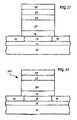
- FIG. 2shows another exemplary embodiment of a memory device 101 constructed in accordance with the invention.
- Memory device 101has many similarities to memory device 100 of FIG. 1 and layers designated with like reference numbers are preferably the same materials and have the same thicknesses as those described in relation to the embodiment shown in FIG. 1 .
- the primary difference between device 100 and device 101is the addition to device 101 of an optional second chalcogenide glass layer 18 a and an optional third chalcogenide glass layer 18 b.
- the optional second chalcogenide glass layer 18 ais formed over the tin-chalcogenide layer 20 , is preferably Ge 40 Se 60 , and is preferably about 150 ⁇ thick. Over this optional second chalcogenide glass layer 18 a is a metal layer 22 , which is preferably silver (Ag) and is preferably about 500 ⁇ thick. Over the metal layer 22 is an optional third chalcogenide glass layer 18 b , which is preferably Ge 40 Se 60 and is preferably about 100 ⁇ thick. The optional third chalcogenide glass layer 18 b provides an adhesion layer for subsequent electrode formation. As with layer 18 of FIG. 1 , layers 18 a and 18 b are not necessarily a single layer, but may be comprised of multiple sub-layers.
- the optional second and third chalcogenide layers 18 a and 18 bmay be a different chalcogenide glass from the first chalcogenide glass layer 18 or from each other.
- Other chalcogenide glassesthat may be useful for this purpose include, but are not limited to, germanium sulfide (GeS), and combination of germanium (Ge), silver (Ag), and selenium (Se).
- a second electrode 24which may be any conductive material, except those that will migrate into the stack and alter memory operation (e.g., Cu or Ag), as discussed above for the preceding embodiments.
- the second electrode 24is tungsten (W).
- FIG. 3shows an exemplary embodiment (where like reference numbers between figures designate like features) in which the memory device 102 does not incorporate a first electrode 16 separate from an address line 12 .
- the memory device 102utilizes a combined address line and electrode structure 12 / 16 , thereby allowing the device to be slightly more simple in design and fabricated in fewer steps than with the embodiments shown in FIGS. 1-2 .
- the address line and electrode structure 12 / 16may be the same materials as discussed above for the first electrode 16 .
- FIG. 4shows a memory device 103 defined, predominantly, by the position of the second electrode 24 .
- the underlying layers of the memory elementi.e., the chalcogenide glass layer 18 , the tin-chalcogenide layer 20 , and the metal layer 22 , are blanket layers formed over a combined address line and electrode structure 12 / 16 and substrate 10 .
- a first electrode 16 separate from an underlying address line 12may be used, as with memory device 100 shown in FIG. 1 .
- the position of the second electrode 24defines the position of the conducting channel formation at the conditioning step and the conductive pathway during operation of the memory device 103 , thus, in this way the second electrode 24 defines the location of the memory device 103 .
- FIG. 5shows an exemplary embodiment (where like reference numbers between figures designate like features) where the memory element is fabricated in a via 28 formed in an insulating layer 14 over an address line and electrode structure 12 / 16 .
- the layers of the memory elementi.e., chalcogenide glass layer 18 , tin-chalcogenide layer 20 , and metal layer 22 , as well as the second electrode 24 are conformally deposited over the insulating layer 14 and substrate 10 and within the via 28 over the address line and electrode structure 12 / 16 .
- the layers 18 , 20 , 22 , and 24are patterned to define a stack over the via 28 , which is etched to form the completed memory device 104 .
- a first electrode 16may be used which is separate from the underlying address line 12 . This separate electrode 16 may also, as another alternative, be formed in the via 28 prior to the formation of the chalcogenide glass layer 18 .
- FIG. 6shows another exemplary embodiment of a memory device 105 constructed in accordance with the invention.
- Memory device 105has many similarities to memory device 100 of FIG. 1 and layers designated with like reference numbers are preferably the same materials and have the same dimensions as those described in relation to the embodiment shown in FIG. 1 .
- Device 105is supported by a substrate 10 and is over an address line 12 .
- the device 105has a first electrode 16 , a chalcogenide glass layer 18 over the first electrode 16 , and a tin-chalcogenide layer 20 over the chalcogenide glass layer 18 .
- the second electrode 24is positioned over the tin-chalcogenide layer 20 and contains a metal, such as silver, which would be available for switching the cell from a low to a high conductivity (high to low resistance).
- FIG. 7shows another exemplary embodiment of a memory device 106 constructed in accordance with the invention.
- Memory device 106has many similarities to memory device 100 of FIG. 1 and device 101 of FIG. 2 and layers designated with like reference numbers are preferably the same materials and have the same dimensions as those described in relation to the embodiment shown in FIGS. 1 and 2 .
- Device 106 of FIG. 7is supported by a substrate 10 and is positioned over an address line 12 .
- Device 106has a first electrode 16 , a chalcogenide glass layer 18 over the first electrode, and a tin-chalcogenide layer 20 over the chalcogenide glass layer 18 .
- a metal layer 22preferably silver, is positioned over the tin-chalcogenide layer 20 .
- a second chalcogenide glass layer 18 aOver the metal layer 22 is positioned a second chalcogenide glass layer 18 a , which may be the same material as the first chalcogenide glass layer 18 .
- FIG. 8shows another exemplary embodiment of a memory device 107 constructed in accordance with the invention.
- Memory device 107has many similarities to memory device 100 of FIG. 1 and layers designated with like reference numbers are preferably the same materials and have the same dimensions as those described in relation to the embodiment shown in FIG. 1 .
- Device 107 of FIG. 8is supported by a substrate 10 and is positioned over an address line 12 .
- Device 107has a first electrode 16 , a chalcogenide glass layer 18 over the first electrode, and a tin-chalcogenide layer 20 over the chalcogenide glass layer 18 .
- an alloy-control layer 21Over the tin-chalcogenide layer 20 is an alloy-control layer 21 , which is preferably selenium (Se) or tin oxide (SnO).
- the alloy-control layer 21can be about 100 ⁇ to about 300 ⁇ thick, preferably about 100 ⁇ thick.
- a metal layer 22preferably silver, is positioned over the alloy-control layer 21 .
- a second electrode 24is positioned over the metal layer 22 .
- the addition of an alloy-control layer 21(above or below the tin-chalcogenide layer 20 ) improves the electrical performance of a PCRAM cell.
- a PCRAM stackmay be formed with an alloy-control layer 21 of Se or SnO in two different locations: above the tin-chalcogenide layer 20 and below the tin-chalcogenide layer 20 . Both of these cases show good electrical switching.
- Improvementsinclude data retention and possibly cycling, as well as a decrease in the read disturb of the OFF state.
- the read disturbis the tendency of the device to turn ON after reading multiple times when it is programmed to the OFF state.
- FIG. 9shows another exemplary embodiment of a memory device 108 constructed in accordance with the invention.
- Memory device 108has many similarities to memory device 100 of FIG. 1 , device 101 of FIG. 2 , and to device 107 of FIG. 8 and layers designated with like reference numbers are preferably the same materials and have the same dimensions as those described in relation to the embodiment shown in FIGS. 1 , 2 and 8 .
- Device 108 of FIG. 9is supported by a substrate 10 and is positioned over an address line 12 .
- Device 108has a first electrode 16 , a chalcogenide glass layer 18 over the first electrode, and a tin-chalcogenide layer 20 over the chalcogenide glass layer 18 .
- An alloy-control layer 21is provided over the tin-chalcogenide layer 20 .
- a second chalcogenide glass layer 18 awhich may be the same material as the first chalcogenide glass layer 18 .
- a metal layer 22preferably silver, is positioned over the second chalcogenide glass layer 18 a .
- a third chalcogenide glass layer 18 bOver the metal layer 22 , is a third chalcogenide glass layer 18 b , which may be the same material as the first two chalcogenide glass layers 18 and 18 b .
- a second electrode 24Over the third chalcogenide glass layer 18 b is a second electrode 24 .
- FIG. 10shows another exemplary embodiment of a memory device 109 constructed in accordance with the invention.
- Memory device 109has many similarities to memory device 100 of FIG. 1 , device 101 of FIG. 2 , device 107 of FIG. 8 , and to device 108 of FIG. 9 and layers designated with like reference numbers are preferably the same materials and have the same dimensions as those described in relation to the embodiment shown in FIGS. 1 , 2 , 8 and 9 .
- Device 109 of FIG. 10is supported by a substrate 10 and is positioned over an address line 12 .
- Device 108has a first electrode 16 and a chalcogenide glass layer 18 over the first electrode.
- An alloy-control layer 21is provided over the chalcogenide glass layer 18 .
- a tin-chalcogenide layer 20is over the alloy-control layer 21 .
- a second chalcogenide glass layer 18 awhich may be the same material as the first chalcogenide glass layer 18 .
- a metal layer 22preferably silver, is positioned over the second chalcogenide glass layer 18 a .
- a third chalcogenide glass layer 18 bis Over the metal layer 22 , which is a third chalcogenide glass layer 18 b , which may be the same material as the first two chalcogenide glass layers 18 and 18 b .
- a second electrode 24Over the third chalcogenide glass layer 18 b is a second electrode 24 .
- FIGS. 11-14illustrate a cross-sectional view of a wafer during the fabrication of a memory device 100 as shown by FIG. 1 .
- FIGS. 11-14most specifically refer to memory device 100 of FIG. 1 , the methods and techniques discussed may also be used to fabricate memory devices 101 - 109 as would be understood by a person of ordinary skill in the art based on a reading of this specification.
- a substrate 10is provided.
- the substrate 10can be semiconductor-based or another material useful as a supporting structure as is known in the art.
- an optional insulating layer(not shown) may be formed over the substrate 10 ; the optional insulating layer may be silicon nitride or other insulating materials used in the art.
- a conductive address line 12is, formed by depositing a conductive material, such as doped polysilicon, aluminum, platinum, silver, gold, nickel, but preferably tungsten, patterning one or more conductive lines, for instance with photolithographic techniques, and etching to define the address line 12 .
- the conductive materialmaybe deposited by any technique known in the art, such as sputtering, chemical vapor deposition, plasma enhanced chemical vapor deposition, evaporation, or plating.
- an insulating layer 14over the address line 12 is formed an insulating layer 14 .
- This layer 14can be silicon nitride, a low dielectric constant material, or many other insulators known in the art that do not allow silver ion migration, and may be deposited by any method known in the art.
- An opening 14 a in the insulating layeris made, for instance by photolithographic and etching techniques, thereby exposing a portion of the underlying address line 12 .
- a conductive materialpreferably tungsten (W).
- a chemical mechanical polishing stepmay then be utilized to remove the conductive material from over the insulating layer 14 , to leave it as a first electrode 16 over the address line 12 , and planarize the wafer.
- FIG. 12shows the cross-section of the wafer of FIG. 11 at a subsequent stage of processing.
- a series of layers making up the memory device 100( FIG. 1 ) are blanket-deposited over the wafer.
- a chalcogenide glass layer 18is formed to a preferred thickness of about 300 ⁇ over the first electrode 16 and insulating layer 14 .
- the chalcogenide glass layer 18is preferably Ge 40 Se 60 .
- this chalcogenide glass layer 18may be accomplished by any suitable method, such as evaporative techniques or chemical vapor deposition using germanium tetrahydride (GeH 4 ) and selenium dihydride (SeH 2 ) gases; however, the preferred technique utilizes either sputtering from a germanium selenide target having the desired stoichiometry or co-sputtering germanium and selenium in the appropriate ratios.
- germanium tetrahydrideGeH 4
- SeH 2selenium dihydride
- a tin-chalcogenide layer 20is formed over the chalcogenide glass layer 18 .
- the tin-chalcogenide layer 20is preferably tin selenide (Sn 1+/ ⁇ x Se, x being between about 1 and 0).
- Physical vapor deposition, chemical vapor deposition, co-evaporation, sputtering, or other techniques known in the artmay be used to deposit layer 20 to a preferred thickness of about 500 ⁇ .
- the thickness of layer 20is selected based, in part, on the thickness of layer 18 and the ratio of the thickness of the tin-chalcogenide layer 20 to that of the underlying chalcogenide glass layer 18 is preferably from about 5:1 to about 1:1, more preferably about 2.5:1. It should be noted that, as the processing steps outlined in relation to FIGS. 11-14 may be adapted for the formation of devices in accordance with those shown in FIGS. 2-10 , an alloy-control layer 21 as shown in devices 107 - 109 may be formed adjacent to the tin-chalcogenide layer 20 , on either side thereof.
- a metal layer 22is formed over the tin-chalcogenide layer 20 .
- the metal layer 22is preferably silver (Ag), or at least contains silver, and is formed to a preferred thickness of about 300 ⁇ .
- the metal layer 22may be deposited by any technique known in the art.
- a conductive materialis deposited for a second electrode 24 .
- this conductive materialmay be any material suitable for a conductive electrode, but is preferably tungsten; however other materials may be used such as titanium nitride or tantalum, for example.
- a layer of photoresist 30is deposited over the top electrode 24 layer, masked and patterned to define the stacks for the memory device 100 , which is but one of a plurality of like memory devices of a memory array.
- An etching stepis used to remove portions of layers 18 , 20 , 22 , and 24 , with the insulating layer 14 used as an etch stop, leaving stacks as shown in FIG. 13 .
- the photoresist 30is removed, leaving a substantially complete memory device 100 , as shown by FIG. 14 .
- An insulating layer 26may be formed over the device 100 to achieve a structure as shown by FIG. 1 . This isolation step can be followed by the forming of connections to other circuitry of the integrated circuit (e.g., logic circuitry, sense amplifiers, etc.) of which the memory device 100 is a part, as is known in the art.
- a conditioning stepis performed by applying a voltage pulse of a given duration and magnitude to incorporate material from the tin-chalcogenide layer 20 into the chalcogenide glass layer 18 to form a conducting channel in the chalcogenide glass layer 18 .
- the conducting channelwill support a conductive pathway during operation of the memory device 100 .
- FIG. 15illustrates a typical processor system 400 which includes a memory circuit 448 , e.g., a PCRAM device, which employs resistance variable memory devices (e.g., device 100 - 109 ) fabricated in accordance with the invention.
- a processor systemsuch as a computer system, generally comprises a central processing unit (CPU) 444 , such as a microprocessor, a digital signal processor, or other programmable digital logic devices, which communicates with an input/output (I/O) device 446 over a bus 452 .
- the memory circuit 448communicates with the CPU 444 over bus 452 typically through a memory controller.
- the processor systemmay include peripheral devices such as a floppy disk drive 454 and a compact disc (CD) ROM drive 456 , which also communicate with CPU 444 over the bus 452 .
- Memory circuit 448is preferably constructed as an integrated circuit, which includes one or more resistance variable memory devices, e.g., device 100 . If desired, the memory circuit 448 may be combined with the processor, for example CPU 444 , in a single integrated circuit.
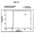
- FIGS. 16 a - 17 bare graphs relating to experimental results obtained from experiments with actual devices having a structure in accordance with the exemplary embodiment shown in FIG. 2 .
- the devices testedhave a tungsten bottom electrode (e.g., layer 16 ), a first 300 ⁇ layer of Ge 40 Se 60 (e.g., layer 18 ) over the bottom electrode, 500 ⁇ layer of SnSe (e.g., layer 20 ) over the Ge 40 Se 60 layer, a second 150 ⁇ layer of Ge 40 Se 60 (e.g., layer 18 a ) over the SnSe layer, a 500 ⁇ layer of silver (Ag) (e.g., layer 22 ) over the second layer of Ge 40 Se 60 , a third 100 ⁇ layer of Ge 40 Se 60 (e.g., layer 18 b ) over the silver layer, and a tungsten top electrode (e.g., layer 24 ).
- a tungsten bottom electrodee.g., layer 16
- the experiments on these deviceswere performed using electrical probing to operate each device.
- a first probewas placed at the top electrode (e.g., layer 24 ) and a second probe was placed at the bottom electrode (e.g., layer 16 ). Potentials were applied between the two probes.
- These tested devicesexhibited improved thermal characteristics relative to previous PCRAM devices.
- the arrayexhibited at least a 90% yield in operational memory devices when processing included an anneal at a temperature of 260° C. for 5 minutes.
- Ninety percent yieldrefers to the percentage of functional devices out of the total number measured. Out of every 100 devices measured, about 90 were functional memory devices at room temperature without an anneal and about 90 out of 100 worked after a 260° C. anneal. Thus, statistically, there is no change in the total number of functional devices post-anneal.
- FIGS. 16 a and 16 bshow how the device switches in response to a DC voltage sweep.
- FIG. 16 ais a DC switching I-V (current vs. voltage) trace, which shows that the devices tested switched from a less conductive state to a higher conductive state at about 0.2 V during a write voltage sweep.
- FIG. 16 bshows a DC switching I-V trace, which shows that the devices erased, or switched from a higher conductive state to a lower conductive state, at about ⁇ 0.5 V and using less than 3 micro-amps of current during a DC voltage sweep.
- the graph of FIG. 17 ais a continuous wave device response voltage vs. time trace, which shows how the tested device responds to a continuous wave signal across the device.
- the deviceOn the positive voltage side, the device is programmed to its lower resistance state and “follows” the input signal.
- FIG. 17 bis a graph relating the voltage across the memory device to the input voltage. As shown, the “threshold voltage” in this example is about 0.4 V to switch the device to its more conductive state and about ⁇ 0.3 V to switch the device to its less conductive state.
Landscapes
- Engineering & Computer Science (AREA)
- Manufacturing & Machinery (AREA)
- Semiconductor Memories (AREA)
- Compositions Of Oxide Ceramics (AREA)
- Inorganic Insulating Materials (AREA)
- Glass Compositions (AREA)
Abstract
Description
Claims (17)
Priority Applications (1)
| Application Number | Priority Date | Filing Date | Title |
|---|---|---|---|
| US11/700,912US7282783B2 (en) | 2004-07-19 | 2007-02-01 | Resistance variable memory device and method of fabrication |
Applications Claiming Priority (2)
| Application Number | Priority Date | Filing Date | Title |
|---|---|---|---|
| US10/893,299US7190048B2 (en) | 2004-07-19 | 2004-07-19 | Resistance variable memory device and method of fabrication |
| US11/700,912US7282783B2 (en) | 2004-07-19 | 2007-02-01 | Resistance variable memory device and method of fabrication |
Related Parent Applications (1)
| Application Number | Title | Priority Date | Filing Date |
|---|---|---|---|
| US10/893,299DivisionUS7190048B2 (en) | 2004-07-19 | 2004-07-19 | Resistance variable memory device and method of fabrication |
Publications (2)
| Publication Number | Publication Date |
|---|---|
| US20070138598A1 US20070138598A1 (en) | 2007-06-21 |
| US7282783B2true US7282783B2 (en) | 2007-10-16 |
Family
ID=35285580
Family Applications (4)
| Application Number | Title | Priority Date | Filing Date |
|---|---|---|---|
| US10/893,299Expired - LifetimeUS7190048B2 (en) | 2004-07-19 | 2004-07-19 | Resistance variable memory device and method of fabrication |
| US11/511,312Expired - LifetimeUS7348209B2 (en) | 2004-07-19 | 2006-08-29 | Resistance variable memory device and method of fabrication |
| US11/700,912Expired - LifetimeUS7282783B2 (en) | 2004-07-19 | 2007-02-01 | Resistance variable memory device and method of fabrication |
| US12/068,108Expired - LifetimeUS7868310B2 (en) | 2004-07-19 | 2008-02-01 | Resistance variable memory device and method of fabrication |
Family Applications Before (2)
| Application Number | Title | Priority Date | Filing Date |
|---|---|---|---|
| US10/893,299Expired - LifetimeUS7190048B2 (en) | 2004-07-19 | 2004-07-19 | Resistance variable memory device and method of fabrication |
| US11/511,312Expired - LifetimeUS7348209B2 (en) | 2004-07-19 | 2006-08-29 | Resistance variable memory device and method of fabrication |
Family Applications After (1)
| Application Number | Title | Priority Date | Filing Date |
|---|---|---|---|
| US12/068,108Expired - LifetimeUS7868310B2 (en) | 2004-07-19 | 2008-02-01 | Resistance variable memory device and method of fabrication |
Country Status (9)
| Country | Link |
|---|---|
| US (4) | US7190048B2 (en) |
| EP (1) | EP1769507B1 (en) |
| JP (2) | JP5107037B2 (en) |
| KR (1) | KR100917095B1 (en) |
| CN (1) | CN100530432C (en) |
| AT (1) | ATE450042T1 (en) |
| DE (1) | DE602005017899D1 (en) |
| TW (1) | TWI293509B (en) |
| WO (1) | WO2006019845A1 (en) |
Cited By (10)
| Publication number | Priority date | Publication date | Assignee | Title |
|---|---|---|---|---|
| US20080121859A1 (en)* | 2006-10-19 | 2008-05-29 | Boise State University | Forced ion migration for chalcogenide phase change memory device |
| US20090289290A1 (en)* | 2008-05-20 | 2009-11-26 | Seagate Technology Llc | Non-volatile memory with programmable capacitance |
| US20090289240A1 (en)* | 2008-05-20 | 2009-11-26 | Seagate Technology Llc | Non-volatile multi-bit memory with programmable capacitance |
| US20100027324A1 (en)* | 2008-08-01 | 2010-02-04 | Boise State University | Variable integrated analog resistor |
| US20110079709A1 (en)* | 2009-10-07 | 2011-04-07 | Campbell Kristy A | Wide band sensor |
| US8284590B2 (en) | 2010-05-06 | 2012-10-09 | Boise State University | Integratable programmable capacitive device |
| US8467236B2 (en) | 2008-08-01 | 2013-06-18 | Boise State University | Continuously variable resistor |
| TWI418070B (en)* | 2009-06-15 | 2013-12-01 | Macronix Int Co Ltd | Phase change memory having stabilized microstructure and manufacturing method |
| US9583699B2 (en) | 2015-06-01 | 2017-02-28 | Boise State University | Tunable variable resistance memory device |
| US9583703B2 (en) | 2015-06-01 | 2017-02-28 | Boise State University | Tunable variable resistance memory device |
Families Citing this family (22)
| Publication number | Priority date | Publication date | Assignee | Title |
|---|---|---|---|---|
| US7190048B2 (en)* | 2004-07-19 | 2007-03-13 | Micron Technology, Inc. | Resistance variable memory device and method of fabrication |
| US7326950B2 (en) | 2004-07-19 | 2008-02-05 | Micron Technology, Inc. | Memory device with switching glass layer |
| DE102004054558A1 (en)* | 2004-11-11 | 2006-05-24 | Infineon Technologies Ag | Phase change random access memory cell manufacturing method, involves back etching portion of structured hard mask by isotropic etching and back etching upper electrode layer and switching active layer by dry etching |
| US7317200B2 (en) | 2005-02-23 | 2008-01-08 | Micron Technology, Inc. | SnSe-based limited reprogrammable cell |
| US7274034B2 (en)* | 2005-08-01 | 2007-09-25 | Micron Technology, Inc. | Resistance variable memory device with sputtered metal-chalcogenide region and method of fabrication |
| US7332735B2 (en)* | 2005-08-02 | 2008-02-19 | Micron Technology, Inc. | Phase change memory cell and method of formation |
| US7767992B2 (en)* | 2005-08-09 | 2010-08-03 | Ovonyx, Inc. | Multi-layer chalcogenide devices |
| US7381982B2 (en)* | 2005-08-26 | 2008-06-03 | Macronix International Co., Ltd. | Method for fabricating chalcogenide-applied memory |
| US20070045606A1 (en)* | 2005-08-30 | 2007-03-01 | Michele Magistretti | Shaping a phase change layer in a phase change memory cell |
| US8188454B2 (en)* | 2005-10-28 | 2012-05-29 | Ovonyx, Inc. | Forming a phase change memory with an ovonic threshold switch |
| US7692272B2 (en)* | 2006-01-19 | 2010-04-06 | Elpida Memory, Inc. | Electrically rewritable non-volatile memory element and method of manufacturing the same |
| US8038850B2 (en)* | 2006-06-23 | 2011-10-18 | Qimonda Ag | Sputter deposition method for forming integrated circuit |
| US20080073751A1 (en)* | 2006-09-21 | 2008-03-27 | Rainer Bruchhaus | Memory cell and method of manufacturing thereof |
| KR100983175B1 (en)* | 2008-07-03 | 2010-09-20 | 광주과학기술원 | A resistance change memory device comprising an oxide film and a solid electrolyte film, and an operation method thereof |
| KR100990215B1 (en)* | 2008-07-17 | 2010-10-29 | 한국전자통신연구원 | Phase change memory device and manufacturing method thereof |
| US7825479B2 (en)* | 2008-08-06 | 2010-11-02 | International Business Machines Corporation | Electrical antifuse having a multi-thickness dielectric layer |
| US8227785B2 (en)* | 2010-11-11 | 2012-07-24 | Micron Technology, Inc. | Chalcogenide containing semiconductors with chalcogenide gradient |
| CN102832338B (en)* | 2012-09-06 | 2015-10-07 | 中国科学院上海微系统与信息技术研究所 | A kind of limiting structure phase transition storage and preparation method thereof |
| CN105378959A (en)* | 2013-03-03 | 2016-03-02 | Adesto技术公司 | Programmable impedance memory elements and corresponding methods |
| KR101431656B1 (en)* | 2013-04-05 | 2014-08-21 | 한국과학기술연구원 | Chacogenide switching device using germanium and selenium and manufacture method thereof |
| KR102488896B1 (en) | 2015-03-31 | 2023-01-17 | 소니 세미컨덕터 솔루션즈 가부시키가이샤 | switch element and memory |
| CN107615611A (en) | 2015-04-30 | 2018-01-19 | 依顿科技有限公司 | power supply control |
Citations (188)
| Publication number | Priority date | Publication date | Assignee | Title |
|---|---|---|---|---|
| US3271591A (en) | 1963-09-20 | 1966-09-06 | Energy Conversion Devices Inc | Symmetrical current controlling device |
| US3622319A (en) | 1966-10-20 | 1971-11-23 | Western Electric Co | Nonreflecting photomasks and methods of making same |
| US3743847A (en) | 1971-06-01 | 1973-07-03 | Motorola Inc | Amorphous silicon film as a uv filter |
| US3961314A (en) | 1974-03-05 | 1976-06-01 | Energy Conversion Devices, Inc. | Structure and method for producing an image |
| US3966317A (en) | 1974-04-08 | 1976-06-29 | Energy Conversion Devices, Inc. | Dry process production of archival microform records from hard copy |
| US3983542A (en) | 1970-08-13 | 1976-09-28 | Energy Conversion Devices, Inc. | Method and apparatus for recording information |
| US4177474A (en) | 1977-05-18 | 1979-12-04 | Energy Conversion Devices, Inc. | High temperature amorphous semiconductor member and method of making the same |
| US4267261A (en) | 1971-07-15 | 1981-05-12 | Energy Conversion Devices, Inc. | Method for full format imaging |
| US4269935A (en) | 1979-07-13 | 1981-05-26 | Ionomet Company, Inc. | Process of doping silver image in chalcogenide layer |
| JPS56126916U (en) | 1980-02-29 | 1981-09-26 | ||
| US4312938A (en) | 1979-07-06 | 1982-01-26 | Drexler Technology Corporation | Method for making a broadband reflective laser recording and data storage medium with absorptive underlayer |
| US4316946A (en) | 1979-12-03 | 1982-02-23 | Ionomet Company, Inc. | Surface sensitized chalcogenide product and process for making and using the same |
| US4320191A (en) | 1978-11-07 | 1982-03-16 | Nippon Telegraph & Telephone Public Corporation | Pattern-forming process |
| US4405710A (en) | 1981-06-22 | 1983-09-20 | Cornell Research Foundation, Inc. | Ion beam exposure of (g-Gex -Se1-x) inorganic resists |
| US4419421A (en) | 1979-01-15 | 1983-12-06 | Max-Planck-Gesellschaft Zur Forderung Der Wissenschaften E.V. | Ion conductor material |
| US4499557A (en) | 1980-10-28 | 1985-02-12 | Energy Conversion Devices, Inc. | Programmable cell for use in programmable electronic arrays |
| US4597162A (en) | 1983-01-18 | 1986-07-01 | Energy Conversion Devices, Inc. | Method for making, parallel preprogramming or field programming of electronic matrix arrays |
| US4608296A (en) | 1983-12-06 | 1986-08-26 | Energy Conversion Devices, Inc. | Superconducting films and devices exhibiting AC to DC conversion |
| US4637895A (en) | 1985-04-01 | 1987-01-20 | Energy Conversion Devices, Inc. | Gas mixtures for the vapor deposition of semiconductor material |
| US4646266A (en) | 1984-09-28 | 1987-02-24 | Energy Conversion Devices, Inc. | Programmable semiconductor structures and methods for using the same |
| US4664939A (en) | 1985-04-01 | 1987-05-12 | Energy Conversion Devices, Inc. | Vertical semiconductor processor |
| US4668968A (en) | 1984-05-14 | 1987-05-26 | Energy Conversion Devices, Inc. | Integrated circuit compatible thin film field effect transistor and method of making same |
| US4670763A (en) | 1984-05-14 | 1987-06-02 | Energy Conversion Devices, Inc. | Thin film field effect transistor |
| US4671618A (en) | 1986-05-22 | 1987-06-09 | Wu Bao Gang | Liquid crystalline-plastic material having submillisecond switch times and extended memory |
| US4673957A (en) | 1984-05-14 | 1987-06-16 | Energy Conversion Devices, Inc. | Integrated circuit compatible thin film field effect transistor and method of making same |
| US4678679A (en) | 1984-06-25 | 1987-07-07 | Energy Conversion Devices, Inc. | Continuous deposition of activated process gases |
| US4710899A (en) | 1985-06-10 | 1987-12-01 | Energy Conversion Devices, Inc. | Data storage medium incorporating a transition metal for increased switching speed |
| US4728406A (en) | 1986-08-18 | 1988-03-01 | Energy Conversion Devices, Inc. | Method for plasma - coating a semiconductor body |
| US4737379A (en) | 1982-09-24 | 1988-04-12 | Energy Conversion Devices, Inc. | Plasma deposited coatings, and low temperature plasma method of making same |
| US4766471A (en) | 1986-01-23 | 1988-08-23 | Energy Conversion Devices, Inc. | Thin film electro-optical devices |
| US4769338A (en) | 1984-05-14 | 1988-09-06 | Energy Conversion Devices, Inc. | Thin film field effect transistor and method of making same |
| US4775425A (en) | 1987-07-27 | 1988-10-04 | Energy Conversion Devices, Inc. | P and n-type microcrystalline semiconductor alloy material including band gap widening elements, devices utilizing same |
| US4788594A (en) | 1986-10-15 | 1988-11-29 | Energy Conversion Devices, Inc. | Solid state electronic camera including thin film matrix of photosensors |
| US4795657A (en) | 1984-04-13 | 1989-01-03 | Energy Conversion Devices, Inc. | Method of fabricating a programmable array |
| US4800526A (en) | 1987-05-08 | 1989-01-24 | Gaf Corporation | Memory element for information storage and retrieval system and associated process |
| US4809044A (en) | 1986-08-22 | 1989-02-28 | Energy Conversion Devices, Inc. | Thin film overvoltage protection devices |
| US4818717A (en) | 1986-06-27 | 1989-04-04 | Energy Conversion Devices, Inc. | Method for making electronic matrix arrays |
| US4843443A (en) | 1984-05-14 | 1989-06-27 | Energy Conversion Devices, Inc. | Thin film field effect transistor and method of making same |
| US4845533A (en) | 1986-08-22 | 1989-07-04 | Energy Conversion Devices, Inc. | Thin film electrical devices with amorphous carbon electrodes and method of making same |
| US4847674A (en) | 1987-03-10 | 1989-07-11 | Advanced Micro Devices, Inc. | High speed interconnect system with refractory non-dogbone contacts and an active electromigration suppression mechanism |
| US4853785A (en) | 1986-10-15 | 1989-08-01 | Energy Conversion Devices, Inc. | Electronic camera including electronic signal storage cartridge |
| US4891330A (en) | 1987-07-27 | 1990-01-02 | Energy Conversion Devices, Inc. | Method of fabricating n-type and p-type microcrystalline semiconductor alloy material including band gap widening elements |
| EP0479325A2 (en) | 1990-10-05 | 1992-04-08 | Energy Conversion Devices, Inc. | Vertically interconnected parallel distributed processor |
| US5128099A (en) | 1991-02-15 | 1992-07-07 | Energy Conversion Devices, Inc. | Congruent state changeable optical memory material and device |
| US5166758A (en) | 1991-01-18 | 1992-11-24 | Energy Conversion Devices, Inc. | Electrically erasable phase change memory |
| US5177567A (en) | 1991-07-19 | 1993-01-05 | Energy Conversion Devices, Inc. | Thin-film structure for chalcogenide electrical switching devices and process therefor |
| US5219788A (en) | 1991-02-25 | 1993-06-15 | Ibm Corporation | Bilayer metallization cap for photolithography |
| US5238862A (en) | 1992-03-18 | 1993-08-24 | Micron Technology, Inc. | Method of forming a stacked capacitor with striated electrode |
| US5272359A (en) | 1988-04-07 | 1993-12-21 | California Institute Of Technology | Reversible non-volatile switch based on a TCNQ charge transfer complex |
| US5296716A (en) | 1991-01-18 | 1994-03-22 | Energy Conversion Devices, Inc. | Electrically erasable, directly overwritable, multibit single cell memory elements and arrays fabricated therefrom |
| US5314772A (en) | 1990-10-09 | 1994-05-24 | Arizona Board Of Regents | High resolution, multi-layer resist for microlithography and method therefor |
| US5315131A (en) | 1990-11-22 | 1994-05-24 | Matsushita Electric Industrial Co., Ltd. | Electrically reprogrammable nonvolatile memory device |
| US5335219A (en) | 1991-01-18 | 1994-08-02 | Ovshinsky Stanford R | Homogeneous composition of microcrystalline semiconductor material, semiconductor devices and directly overwritable memory elements fabricated therefrom, and arrays fabricated from the memory elements |
| US5341328A (en) | 1991-01-18 | 1994-08-23 | Energy Conversion Devices, Inc. | Electrically erasable memory elements having reduced switching current requirements and increased write/erase cycle life |
| US5350484A (en) | 1992-09-08 | 1994-09-27 | Intel Corporation | Method for the anisotropic etching of metal films in the fabrication of interconnects |
| US5359205A (en) | 1991-11-07 | 1994-10-25 | Energy Conversion Devices, Inc. | Electrically erasable memory elements characterized by reduced current and improved thermal stability |
| US5360981A (en) | 1989-05-11 | 1994-11-01 | British Telecommunications Public Limited Company | Amorphous silicon memory |
| US5406509A (en) | 1991-01-18 | 1995-04-11 | Energy Conversion Devices, Inc. | Electrically erasable, directly overwritable, multibit single cell memory elements and arrays fabricated therefrom |
| US5414271A (en) | 1991-01-18 | 1995-05-09 | Energy Conversion Devices, Inc. | Electrically erasable memory elements having improved set resistance stability |
| US5500532A (en) | 1994-08-18 | 1996-03-19 | Arizona Board Of Regents | Personal electronic dosimeter |
| US5512328A (en) | 1992-08-07 | 1996-04-30 | Hitachi, Ltd. | Method for forming a pattern and forming a thin film used in pattern formation |
| US5512773A (en) | 1993-12-23 | 1996-04-30 | U.S. Philips Corporation | Switching element with memory provided with Schottky tunnelling barrier |
| US5534712A (en) | 1991-01-18 | 1996-07-09 | Energy Conversion Devices, Inc. | Electrically erasable memory elements characterized by reduced current and improved thermal stability |
| US5534711A (en) | 1991-01-18 | 1996-07-09 | Energy Conversion Devices, Inc. | Electrically erasable, directly overwritable, multibit single cell memory elements and arrays fabricated therefrom |
| US5536947A (en) | 1991-01-18 | 1996-07-16 | Energy Conversion Devices, Inc. | Electrically erasable, directly overwritable, multibit single cell memory element and arrays fabricated therefrom |
| US5543737A (en) | 1995-02-10 | 1996-08-06 | Energy Conversion Devices, Inc. | Logical operation circuit employing two-terminal chalcogenide switches |
| US5591501A (en) | 1995-12-20 | 1997-01-07 | Energy Conversion Devices, Inc. | Optical recording medium having a plurality of discrete phase change data recording points |
| US5596522A (en) | 1991-01-18 | 1997-01-21 | Energy Conversion Devices, Inc. | Homogeneous compositions of microcrystalline semiconductor material, semiconductor devices and directly overwritable memory elements fabricated therefrom, and arrays fabricated from the memory elements |
| US5687112A (en) | 1996-04-19 | 1997-11-11 | Energy Conversion Devices, Inc. | Multibit single cell memory element having tapered contact |
| US5694054A (en) | 1995-11-28 | 1997-12-02 | Energy Conversion Devices, Inc. | Integrated drivers for flat panel displays employing chalcogenide logic elements |
| WO1997048032A2 (en) | 1996-05-30 | 1997-12-18 | Axon Technologies Corporation | Programmable metallization cell and method of making |
| US5714768A (en) | 1995-10-24 | 1998-02-03 | Energy Conversion Devices, Inc. | Second-layer phase change memory array on top of a logic device |
| US5726083A (en) | 1994-11-29 | 1998-03-10 | Nec Corporation | Process of fabricating dynamic random access memory device having storage capacitor low in contact resistance and small in leakage current through tantalum oxide film |
| US5751012A (en) | 1995-06-07 | 1998-05-12 | Micron Technology, Inc. | Polysilicon pillar diode for use in a non-volatile memory cell |
| US5789277A (en) | 1996-07-22 | 1998-08-04 | Micron Technology, Inc. | Method of making chalogenide memory device |
| US5814527A (en) | 1996-07-22 | 1998-09-29 | Micron Technology, Inc. | Method of making small pores defined by a disposable internal spacer for use in chalcogenide memories |
| US5818749A (en) | 1993-08-20 | 1998-10-06 | Micron Technology, Inc. | Integrated circuit memory device |
| US5825046A (en) | 1996-10-28 | 1998-10-20 | Energy Conversion Devices, Inc. | Composite memory material comprising a mixture of phase-change memory material and dielectric material |
| US5841150A (en) | 1995-06-07 | 1998-11-24 | Micron Technology, Inc. | Stack/trench diode for use with a muti-state material in a non-volatile memory cell |
| US5846889A (en) | 1997-03-14 | 1998-12-08 | The United States Of America As Represented By The Secretary Of The Navy | Infrared transparent selenide glasses |
| US5851882A (en) | 1996-05-06 | 1998-12-22 | Micron Technology, Inc. | ZPROM manufacture and design and methods for forming thin structures using spacers as an etching mask |
| US5869843A (en) | 1995-06-07 | 1999-02-09 | Micron Technology, Inc. | Memory array having a multi-state element and method for forming such array or cells thereof |
| US5912839A (en) | 1998-06-23 | 1999-06-15 | Energy Conversion Devices, Inc. | Universal memory element and method of programming same |
| US5920788A (en) | 1995-06-07 | 1999-07-06 | Micron Technology, Inc. | Chalcogenide memory cell with a plurality of chalcogenide electrodes |
| US5933365A (en) | 1997-06-19 | 1999-08-03 | Energy Conversion Devices, Inc. | Memory element with energy control mechanism |
| WO1999028914A3 (en) | 1997-12-04 | 1999-08-26 | Axon Technologies Corp | Programmable sub-surface aggregating metallization structure and method of making same |
| US5998066A (en) | 1997-05-16 | 1999-12-07 | Aerial Imaging Corporation | Gray scale mask and depth pattern transfer technique using inorganic chalcogenide glass |
| US6011757A (en) | 1998-01-27 | 2000-01-04 | Ovshinsky; Stanford R. | Optical recording media having increased erasability |
| US6031287A (en) | 1997-06-18 | 2000-02-29 | Micron Technology, Inc. | Contact structure and memory element incorporating the same |
| US6072716A (en) | 1999-04-14 | 2000-06-06 | Massachusetts Institute Of Technology | Memory structures and methods of making same |
| US6087674A (en) | 1996-10-28 | 2000-07-11 | Energy Conversion Devices, Inc. | Memory element with memory material comprising phase-change material and dielectric material |
| US6117720A (en) | 1995-06-07 | 2000-09-12 | Micron Technology, Inc. | Method of making an integrated circuit electrode having a reduced contact area |
| US6141241A (en) | 1998-06-23 | 2000-10-31 | Energy Conversion Devices, Inc. | Universal memory element with systems employing same and apparatus and method for reading, writing and programming same |
| US6143604A (en) | 1999-06-04 | 2000-11-07 | Taiwan Semiconductor Manufacturing Company | Method for fabricating small-size two-step contacts for word-line strapping on dynamic random access memory (DRAM) |
| US6177338B1 (en) | 1999-02-08 | 2001-01-23 | Taiwan Semiconductor Manufacturing Company | Two step barrier process |
| US6236059B1 (en) | 1996-08-22 | 2001-05-22 | Micron Technology, Inc. | Memory cell incorporating a chalcogenide element and method of making same |
| US6297170B1 (en) | 1998-06-23 | 2001-10-02 | Vlsi Technology, Inc. | Sacrificial multilayer anti-reflective coating for mos gate formation |
| US6300684B1 (en) | 1995-06-07 | 2001-10-09 | Micron Technology, Inc. | Method for fabricating an array of ultra-small pores for chalcogenide memory cells |
| WO2000048196A9 (en) | 1999-02-11 | 2001-11-01 | Univ Arizona | Programmable microelectronic devices and methods of forming and programming same |
| US6329606B1 (en) | 1996-04-24 | 2001-12-11 | Amkor Technology, Inc. | Grid array assembly of circuit boards with singulation grooves |
| US20020000666A1 (en) | 1998-08-31 | 2002-01-03 | Michael N. Kozicki | Self-repairing interconnections for electrical circuits |
| US6339544B1 (en) | 2000-09-29 | 2002-01-15 | Intel Corporation | Method to enhance performance of thermal resistor device |
| US6348365B1 (en) | 2001-03-02 | 2002-02-19 | Micron Technology, Inc. | PCRAM cell manufacturing |
| US6350679B1 (en) | 1999-08-03 | 2002-02-26 | Micron Technology, Inc. | Methods of providing an interlevel dielectric layer intermediate different elevation conductive metal layers in the fabrication of integrated circuitry |
| WO2002021542A1 (en) | 2000-09-08 | 2002-03-14 | Axon Technologies Corporation | Microelectronic programmable device and methods of forming and programming the same |
| US6376284B1 (en) | 1996-02-23 | 2002-04-23 | Micron Technology, Inc. | Method of fabricating a memory device |
| US6404665B1 (en) | 2000-09-29 | 2002-06-11 | Intel Corporation | Compositionally modified resistive electrode |
| US20020072188A1 (en) | 2000-12-08 | 2002-06-13 | Gilton Terry L. | Non-volatile resistance variable devices and method of forming same, analog memory devices and method of forming same, programmable memory cell and method of forming same, and method of structurally changing a non-volatile device |
| US6414376B1 (en) | 1997-07-31 | 2002-07-02 | Micron Technology, Inc. | Method and apparatus for reducing isolation stress in integrated circuits |
| US6423628B1 (en) | 1999-10-22 | 2002-07-23 | Lsi Logic Corporation | Method of forming integrated circuit structure having low dielectric constant material and having silicon oxynitride caps over closely spaced apart metal lines |
| US6429064B1 (en) | 2000-09-29 | 2002-08-06 | Intel Corporation | Reduced contact area of sidewall conductor |
| US20020106849A1 (en) | 2001-02-08 | 2002-08-08 | Moore John T. | Method of forming non-volatile resistance variable devices, method of precluding diffusion of a metal into adjacent chalcogenide material, and non-volatile resistance variable devices |
| US6437383B1 (en) | 2000-12-21 | 2002-08-20 | Intel Corporation | Dual trench isolation for a phase-change memory cell and method of making same |
| US6440837B1 (en) | 2000-07-14 | 2002-08-27 | Micron Technology, Inc. | Method of forming a contact structure in a semiconductor device |
| US20020123248A1 (en) | 2001-03-01 | 2002-09-05 | Moore John T. | Methods of metal doping a chalcogenide material |
| US20020127886A1 (en) | 2001-03-07 | 2002-09-12 | Moore John T. | Method to manufacture a buried electrode PCRAM cell |
| US20020132417A1 (en) | 2001-03-15 | 2002-09-19 | Jiutao Li | Agglomeration elimination for metal sputter deposition of chalcogenides |
| US6462984B1 (en) | 2001-06-29 | 2002-10-08 | Intel Corporation | Biasing scheme of floating unselected wordlines and bitlines of a diode-based memory array |
| US6469364B1 (en) | 1998-08-31 | 2002-10-22 | Arizona Board Of Regents | Programmable interconnection system for electrical circuits |
| US6473332B1 (en) | 2001-04-04 | 2002-10-29 | The University Of Houston System | Electrically variable multi-state resistance computing |
| US20020160551A1 (en) | 2001-03-15 | 2002-10-31 | Harshfield Steven T. | Memory elements and methods for making same |
| US20020163828A1 (en) | 2001-05-07 | 2002-11-07 | Coatue Corporation | Memory device with a self-assembled polymer film and method of making the same |
| US6480438B1 (en) | 2001-06-12 | 2002-11-12 | Ovonyx, Inc. | Providing equal cell programming conditions across a large and high density array of phase-change memory cells |
| US20020168852A1 (en) | 2001-05-11 | 2002-11-14 | Harshfield Steven T. | PCRAM memory cell and method of making same |
| US20020168820A1 (en) | 2000-09-08 | 2002-11-14 | Kozicki Michael N. | Microelectronic programmable device and methods of forming and programming the same |
| US6487106B1 (en) | 1999-01-12 | 2002-11-26 | Arizona Board Of Regents | Programmable microelectronic devices and method of forming and programming same |
| US6487113B1 (en) | 2001-06-29 | 2002-11-26 | Ovonyx, Inc. | Programming a phase-change memory with slow quench time |
| US6501111B1 (en) | 2000-06-30 | 2002-12-31 | Intel Corporation | Three-dimensional (3D) programmable device |
| US6507061B1 (en) | 2001-08-31 | 2003-01-14 | Intel Corporation | Multiple layer phase-change memory |
| US6511862B2 (en) | 2001-06-30 | 2003-01-28 | Ovonyx, Inc. | Modified contact for programmable devices |
| US6511867B2 (en) | 2001-06-30 | 2003-01-28 | Ovonyx, Inc. | Utilizing atomic layer deposition for programmable device |
| US6512241B1 (en) | 2001-12-31 | 2003-01-28 | Intel Corporation | Phase change material memory device |
| US6514805B2 (en) | 2001-06-30 | 2003-02-04 | Intel Corporation | Trench sidewall profile for device isolation |
| US20030027416A1 (en) | 2001-08-01 | 2003-02-06 | Moore John T. | Method of forming integrated circuitry, method of forming memory circuitry, and method of forming random access memory circuitry |
| US20030035315A1 (en) | 2001-04-06 | 2003-02-20 | Kozicki Michael N. | Microelectronic device, structure, and system, including a memory structure having a variable programmable property and method of forming the same |
| US20030038301A1 (en) | 2001-08-27 | 2003-02-27 | John Moore | Apparatus and method for dual cell common electrode PCRAM memory device |
| US20030045054A1 (en) | 2001-08-29 | 2003-03-06 | Campbell Kristy A. | Method of forming non-volatile resistance variable devices, method of forming a programmable memory cell of memory circuitry, and a non-volatile resistance variable device |
| US20030043631A1 (en) | 2001-08-30 | 2003-03-06 | Gilton Terry L. | Method of retaining memory state in a programmable conductor RAM |
| US20030045049A1 (en) | 2001-08-29 | 2003-03-06 | Campbell Kristy A. | Method of forming chalcogenide comprising devices |
| US6531373B2 (en) | 2000-12-27 | 2003-03-11 | Ovonyx, Inc. | Method of forming a phase-change memory cell using silicon on insulator low electrode in charcogenide elements |
| US20030048519A1 (en) | 2000-02-11 | 2003-03-13 | Kozicki Michael N. | Microelectronic photonic structure and device and method of forming the same |
| US20030048744A1 (en) | 2001-09-01 | 2003-03-13 | Ovshinsky Stanford R. | Increased data storage in optical data storage and retrieval systems using blue lasers and/or plasmon lenses |
| US20030047765A1 (en) | 2001-08-30 | 2003-03-13 | Campbell Kristy A. | Stoichiometry for chalcogenide glasses useful for memory devices and method of formation |
| US20030049912A1 (en) | 2001-08-29 | 2003-03-13 | Campbell Kristy A. | Method of forming chalcogenide comprsing devices and method of forming a programmable memory cell of memory circuitry |
| US6534781B2 (en) | 2000-12-26 | 2003-03-18 | Ovonyx, Inc. | Phase-change memory bipolar array utilizing a single shallow trench isolation for creating an individual active area region for two memory array elements and one bipolar base contact |
| US6545907B1 (en) | 2001-10-30 | 2003-04-08 | Ovonyx, Inc. | Technique and apparatus for performing write operations to a phase change material memory device |
| US6545287B2 (en) | 2001-09-07 | 2003-04-08 | Intel Corporation | Using selective deposition to form phase-change memory cells |
| US20030068862A1 (en) | 2001-08-30 | 2003-04-10 | Jiutao Li | Integrated circuit device and fabrication using metal-doped chalcogenide materials |
| US6555860B2 (en) | 2000-09-29 | 2003-04-29 | Intel Corporation | Compositionally modified resistive electrode |
| US6563164B2 (en) | 2000-09-29 | 2003-05-13 | Ovonyx, Inc. | Compositionally modified resistive electrode |
| US6566700B2 (en) | 2001-10-11 | 2003-05-20 | Ovonyx, Inc. | Carbon-containing interfacial layer for phase-change memory |
| US6567293B1 (en) | 2000-09-29 | 2003-05-20 | Ovonyx, Inc. | Single level metal memory cell using chalcogenide cladding |
| US20030095426A1 (en) | 2001-11-20 | 2003-05-22 | Glen Hush | Complementary bit PCRAM sense amplifier and method of operation |
| US20030096497A1 (en) | 2001-11-19 | 2003-05-22 | Micron Technology, Inc. | Electrode structure for use in an integrated circuit |
| US6569705B2 (en) | 2000-12-21 | 2003-05-27 | Intel Corporation | Metal structure for a phase-change memory device |
| US6570784B2 (en) | 2001-06-29 | 2003-05-27 | Ovonyx, Inc. | Programming a phase-change material memory |
| US6576921B2 (en) | 2001-11-08 | 2003-06-10 | Intel Corporation | Isolating phase change material memory cells |
| US20030107105A1 (en) | 1999-08-31 | 2003-06-12 | Kozicki Michael N. | Programmable chip-to-substrate interconnect structure and device and method of forming same |
| US20030117831A1 (en) | 2001-12-20 | 2003-06-26 | Glen Hush | Programmable conductor random access memory and a method for writing thereto |
| US6586761B2 (en) | 2001-09-07 | 2003-07-01 | Intel Corporation | Phase change material memory device |
| US6590807B2 (en) | 2001-08-02 | 2003-07-08 | Intel Corporation | Method for reading a structural phase-change memory |
| US6589714B2 (en) | 2001-06-26 | 2003-07-08 | Ovonyx, Inc. | Method for making programmable resistance memory element using silylated photoresist |
| US20030128612A1 (en) | 2002-01-04 | 2003-07-10 | John Moore | PCRAM rewrite prevention |
| US20030137869A1 (en) | 1998-12-04 | 2003-07-24 | Kozicki Michael N. | Programmable microelectronic device, structure, and system and method of forming the same |
| US20030143782A1 (en) | 2002-01-31 | 2003-07-31 | Gilton Terry L. | Methods of forming germanium selenide comprising devices and methods of forming silver selenide comprising structures |
| US6605527B2 (en) | 2001-06-30 | 2003-08-12 | Intel Corporation | Reduced area intersection between electrode and programming element |
| US20030156463A1 (en) | 2002-02-19 | 2003-08-21 | Casper Stephen L. | Programmable conductor random access memory and method for sensing same |
| US20030155589A1 (en) | 2002-02-20 | 2003-08-21 | Campbell Kristy A. | Silver-selenide/chalcogenide glass stack for resistance variable memory |
| US20030155606A1 (en) | 2002-02-15 | 2003-08-21 | Campbell Kristy A. | Method to alter chalcogenide glass for improved switching characteristics |
| US20030156447A1 (en) | 2000-02-11 | 2003-08-21 | Kozicki Michael N. | Programming circuit for a programmable microelectronic device, system including the circuit, and method of forming the same |
| US6613604B2 (en) | 2001-08-02 | 2003-09-02 | Ovonyx, Inc. | Method for making small pore for use in programmable resistance memory element |
| US6625054B2 (en) | 2001-12-28 | 2003-09-23 | Intel Corporation | Method and apparatus to program a phase change memory |
| US6642102B2 (en) | 2001-06-30 | 2003-11-04 | Intel Corporation | Barrier material encapsulation of programmable material |
| US6646297B2 (en) | 2000-12-26 | 2003-11-11 | Ovonyx, Inc. | Lower electrode isolation in a double-wide trench |
| US20030212724A1 (en) | 2002-05-10 | 2003-11-13 | Ovshinsky Stanford R. | Methods of computing with digital multistate phase change materials |
| US20030210564A1 (en) | 2001-10-26 | 2003-11-13 | Kozicki Michael N. | Tunable cantilever apparatus and method for making same |
| US20030209971A1 (en) | 2000-02-11 | 2003-11-13 | Kozicki Michael N. | Programmable structure, an array including the structure, and methods of forming the same |
| US6649928B2 (en) | 2000-12-13 | 2003-11-18 | Intel Corporation | Method to selectively remove one side of a conductive bottom electrode of a phase-change memory cell and structure obtained thereby |
| US6667900B2 (en) | 2001-12-28 | 2003-12-23 | Ovonyx, Inc. | Method and apparatus to operate a memory cell |
| US6673700B2 (en) | 2001-06-30 | 2004-01-06 | Ovonyx, Inc. | Reduced area intersection between electrode and programming element |
| US6687427B2 (en) | 2000-12-29 | 2004-02-03 | Intel Corporation | Optic switch |
| US6690026B2 (en) | 2001-09-28 | 2004-02-10 | Intel Corporation | Method of fabricating a three-dimensional array of active media |
| US20040027849A1 (en) | 2000-10-31 | 2004-02-12 | Yang Yang | Organic bistable device and organic memory cells |
| US6696355B2 (en) | 2000-12-14 | 2004-02-24 | Ovonyx, Inc. | Method to selectively increase the top resistance of the lower programming electrode in a phase-change memory |
| US20040035401A1 (en) | 2002-08-26 | 2004-02-26 | Subramanian Ramachandran | Hydrogen powered scooter |
| US20040042265A1 (en) | 2002-08-29 | 2004-03-04 | Moore John T. | Method and apparatus for controlling metal doping of a chalcogenide memory element |
| US6953720B2 (en)* | 2002-08-29 | 2005-10-11 | Micron Technology, Inc. | Methods for forming chalcogenide glass-based memory elements |
| US7015494B2 (en)* | 2002-07-10 | 2006-03-21 | Micron Technology, Inc. | Assemblies displaying differential negative resistance |
Family Cites Families (17)
| Publication number | Priority date | Publication date | Assignee | Title |
|---|---|---|---|---|
| US3980505A (en)* | 1973-09-12 | 1976-09-14 | Buckley William D | Process of making a filament-type memory semiconductor device |
| JP2794348B2 (en)* | 1991-06-21 | 1998-09-03 | キヤノン株式会社 | Recording medium, manufacturing method thereof, and information processing apparatus |
| DE4318825C1 (en)* | 1993-06-07 | 1994-06-09 | Continental Ag | Tyre construction for commercial vehicles - has aramid carcass with ends wrapped round aramid bead cores and these plus belt are made of synthetic fibre-reinforced rubber |
| US5505719A (en)* | 1994-06-30 | 1996-04-09 | Mcneil-Ppc, Inc. | Multilayered absorbent structures |
| US6676900B1 (en)* | 1994-12-09 | 2004-01-13 | Therox, Inc. | Method for the preparation and delivery of gas-enriched fluids |
| JP4025527B2 (en)* | 2000-10-27 | 2007-12-19 | 松下電器産業株式会社 | Memory, writing device, reading device and method thereof |
| US6809362B2 (en) | 2002-02-20 | 2004-10-26 | Micron Technology, Inc. | Multiple data state memory cell |
| US6849868B2 (en)* | 2002-03-14 | 2005-02-01 | Micron Technology, Inc. | Methods and apparatus for resistance variable material cells |
| US6867996B2 (en) | 2002-08-29 | 2005-03-15 | Micron Technology, Inc. | Single-polarity programmable resistance-variable memory element |
| US6864521B2 (en)* | 2002-08-29 | 2005-03-08 | Micron Technology, Inc. | Method to control silver concentration in a resistance variable memory element |
| CN100341060C (en)* | 2002-09-13 | 2007-10-03 | 松下电器产业株式会社 | Information recording medium and its manufacturing method |
| US6795338B2 (en)* | 2002-12-13 | 2004-09-21 | Intel Corporation | Memory having access devices using phase change material such as chalcogenide |
| US6813178B2 (en)* | 2003-03-12 | 2004-11-02 | Micron Technology, Inc. | Chalcogenide glass constant current device, and its method of fabrication and operation |
| JP4254293B2 (en)* | 2003-03-25 | 2009-04-15 | 株式会社日立製作所 | Storage device |
| US7190048B2 (en)* | 2004-07-19 | 2007-03-13 | Micron Technology, Inc. | Resistance variable memory device and method of fabrication |
| US7326950B2 (en)* | 2004-07-19 | 2008-02-05 | Micron Technology, Inc. | Memory device with switching glass layer |
| US7317200B2 (en)* | 2005-02-23 | 2008-01-08 | Micron Technology, Inc. | SnSe-based limited reprogrammable cell |
- 2004
- 2004-07-19USUS10/893,299patent/US7190048B2/ennot_activeExpired - Lifetime
- 2005
- 2005-07-14JPJP2007522567Apatent/JP5107037B2/ennot_activeExpired - Lifetime
- 2005-07-14KRKR1020077003843Apatent/KR100917095B1/ennot_activeExpired - Lifetime
- 2005-07-14CNCNB2005800308295Apatent/CN100530432C/ennot_activeExpired - Lifetime
- 2005-07-14ATAT05772169Tpatent/ATE450042T1/ennot_activeIP Right Cessation
- 2005-07-14DEDE602005017899Tpatent/DE602005017899D1/ennot_activeExpired - Lifetime
- 2005-07-14WOPCT/US2005/024899patent/WO2006019845A1/enactiveApplication Filing
- 2005-07-14EPEP05772169Apatent/EP1769507B1/ennot_activeExpired - Lifetime
- 2005-07-19TWTW094124377Apatent/TWI293509B/ennot_activeIP Right Cessation
- 2006
- 2006-08-29USUS11/511,312patent/US7348209B2/ennot_activeExpired - Lifetime
- 2007
- 2007-02-01USUS11/700,912patent/US7282783B2/ennot_activeExpired - Lifetime
- 2008
- 2008-02-01USUS12/068,108patent/US7868310B2/ennot_activeExpired - Lifetime
- 2011
- 2011-08-11JPJP2011175686Apatent/JP5364762B2/ennot_activeExpired - Lifetime
Patent Citations (225)
| Publication number | Priority date | Publication date | Assignee | Title |
|---|---|---|---|---|
| US3271591A (en) | 1963-09-20 | 1966-09-06 | Energy Conversion Devices Inc | Symmetrical current controlling device |
| US3622319A (en) | 1966-10-20 | 1971-11-23 | Western Electric Co | Nonreflecting photomasks and methods of making same |
| US3983542A (en) | 1970-08-13 | 1976-09-28 | Energy Conversion Devices, Inc. | Method and apparatus for recording information |
| US3988720A (en) | 1970-08-13 | 1976-10-26 | Energy Conversion Devices, Inc. | Recording and retrieving information in an amorphous memory material using a catalytic material |
| US3743847A (en) | 1971-06-01 | 1973-07-03 | Motorola Inc | Amorphous silicon film as a uv filter |
| US4267261A (en) | 1971-07-15 | 1981-05-12 | Energy Conversion Devices, Inc. | Method for full format imaging |
| US3961314A (en) | 1974-03-05 | 1976-06-01 | Energy Conversion Devices, Inc. | Structure and method for producing an image |
| US3966317A (en) | 1974-04-08 | 1976-06-29 | Energy Conversion Devices, Inc. | Dry process production of archival microform records from hard copy |
| US4177474A (en) | 1977-05-18 | 1979-12-04 | Energy Conversion Devices, Inc. | High temperature amorphous semiconductor member and method of making the same |
| US4320191A (en) | 1978-11-07 | 1982-03-16 | Nippon Telegraph & Telephone Public Corporation | Pattern-forming process |
| US4419421A (en) | 1979-01-15 | 1983-12-06 | Max-Planck-Gesellschaft Zur Forderung Der Wissenschaften E.V. | Ion conductor material |
| US4312938A (en) | 1979-07-06 | 1982-01-26 | Drexler Technology Corporation | Method for making a broadband reflective laser recording and data storage medium with absorptive underlayer |
| US4269935A (en) | 1979-07-13 | 1981-05-26 | Ionomet Company, Inc. | Process of doping silver image in chalcogenide layer |
| US4316946A (en) | 1979-12-03 | 1982-02-23 | Ionomet Company, Inc. | Surface sensitized chalcogenide product and process for making and using the same |
| JPS56126916U (en) | 1980-02-29 | 1981-09-26 | ||
| US4499557A (en) | 1980-10-28 | 1985-02-12 | Energy Conversion Devices, Inc. | Programmable cell for use in programmable electronic arrays |
| US4405710A (en) | 1981-06-22 | 1983-09-20 | Cornell Research Foundation, Inc. | Ion beam exposure of (g-Gex -Se1-x) inorganic resists |
| US4737379A (en) | 1982-09-24 | 1988-04-12 | Energy Conversion Devices, Inc. | Plasma deposited coatings, and low temperature plasma method of making same |
| US4597162A (en) | 1983-01-18 | 1986-07-01 | Energy Conversion Devices, Inc. | Method for making, parallel preprogramming or field programming of electronic matrix arrays |
| US4608296A (en) | 1983-12-06 | 1986-08-26 | Energy Conversion Devices, Inc. | Superconducting films and devices exhibiting AC to DC conversion |
| US4795657A (en) | 1984-04-13 | 1989-01-03 | Energy Conversion Devices, Inc. | Method of fabricating a programmable array |
| US4673957A (en) | 1984-05-14 | 1987-06-16 | Energy Conversion Devices, Inc. | Integrated circuit compatible thin film field effect transistor and method of making same |
| US4769338A (en) | 1984-05-14 | 1988-09-06 | Energy Conversion Devices, Inc. | Thin film field effect transistor and method of making same |
| US4670763A (en) | 1984-05-14 | 1987-06-02 | Energy Conversion Devices, Inc. | Thin film field effect transistor |
| US4843443A (en) | 1984-05-14 | 1989-06-27 | Energy Conversion Devices, Inc. | Thin film field effect transistor and method of making same |
| US4668968A (en) | 1984-05-14 | 1987-05-26 | Energy Conversion Devices, Inc. | Integrated circuit compatible thin film field effect transistor and method of making same |
| US4678679A (en) | 1984-06-25 | 1987-07-07 | Energy Conversion Devices, Inc. | Continuous deposition of activated process gases |
| US4646266A (en) | 1984-09-28 | 1987-02-24 | Energy Conversion Devices, Inc. | Programmable semiconductor structures and methods for using the same |
| US4637895A (en) | 1985-04-01 | 1987-01-20 | Energy Conversion Devices, Inc. | Gas mixtures for the vapor deposition of semiconductor material |
| US4696758A (en) | 1985-04-01 | 1987-09-29 | Energy Conversion Devices, Inc. | Gas mixtures for the vapor deposition of semiconductor material |
| US4698234A (en) | 1985-04-01 | 1987-10-06 | Energy Conversion Devices, Inc. | Vapor deposition of semiconductor material |
| US4664939A (en) | 1985-04-01 | 1987-05-12 | Energy Conversion Devices, Inc. | Vertical semiconductor processor |
| US4710899A (en) | 1985-06-10 | 1987-12-01 | Energy Conversion Devices, Inc. | Data storage medium incorporating a transition metal for increased switching speed |
| US4766471A (en) | 1986-01-23 | 1988-08-23 | Energy Conversion Devices, Inc. | Thin film electro-optical devices |
| US4671618A (en) | 1986-05-22 | 1987-06-09 | Wu Bao Gang | Liquid crystalline-plastic material having submillisecond switch times and extended memory |
| US4818717A (en) | 1986-06-27 | 1989-04-04 | Energy Conversion Devices, Inc. | Method for making electronic matrix arrays |
| US4728406A (en) | 1986-08-18 | 1988-03-01 | Energy Conversion Devices, Inc. | Method for plasma - coating a semiconductor body |
| US4809044A (en) | 1986-08-22 | 1989-02-28 | Energy Conversion Devices, Inc. | Thin film overvoltage protection devices |
| US4845533A (en) | 1986-08-22 | 1989-07-04 | Energy Conversion Devices, Inc. | Thin film electrical devices with amorphous carbon electrodes and method of making same |
| US4788594A (en) | 1986-10-15 | 1988-11-29 | Energy Conversion Devices, Inc. | Solid state electronic camera including thin film matrix of photosensors |
| US4853785A (en) | 1986-10-15 | 1989-08-01 | Energy Conversion Devices, Inc. | Electronic camera including electronic signal storage cartridge |
| US4847674A (en) | 1987-03-10 | 1989-07-11 | Advanced Micro Devices, Inc. | High speed interconnect system with refractory non-dogbone contacts and an active electromigration suppression mechanism |
| US4800526A (en) | 1987-05-08 | 1989-01-24 | Gaf Corporation | Memory element for information storage and retrieval system and associated process |
| US4891330A (en) | 1987-07-27 | 1990-01-02 | Energy Conversion Devices, Inc. | Method of fabricating n-type and p-type microcrystalline semiconductor alloy material including band gap widening elements |
| US4775425A (en) | 1987-07-27 | 1988-10-04 | Energy Conversion Devices, Inc. | P and n-type microcrystalline semiconductor alloy material including band gap widening elements, devices utilizing same |
| US5272359A (en) | 1988-04-07 | 1993-12-21 | California Institute Of Technology | Reversible non-volatile switch based on a TCNQ charge transfer complex |
| US5360981A (en) | 1989-05-11 | 1994-11-01 | British Telecommunications Public Limited Company | Amorphous silicon memory |
| EP0479325A2 (en) | 1990-10-05 | 1992-04-08 | Energy Conversion Devices, Inc. | Vertically interconnected parallel distributed processor |
| US5159661A (en) | 1990-10-05 | 1992-10-27 | Energy Conversion Devices, Inc. | Vertically interconnected parallel distributed processor |
| US5314772A (en) | 1990-10-09 | 1994-05-24 | Arizona Board Of Regents | High resolution, multi-layer resist for microlithography and method therefor |
| US5315131A (en) | 1990-11-22 | 1994-05-24 | Matsushita Electric Industrial Co., Ltd. | Electrically reprogrammable nonvolatile memory device |
| US5534711A (en) | 1991-01-18 | 1996-07-09 | Energy Conversion Devices, Inc. | Electrically erasable, directly overwritable, multibit single cell memory elements and arrays fabricated therefrom |
| US5414271A (en) | 1991-01-18 | 1995-05-09 | Energy Conversion Devices, Inc. | Electrically erasable memory elements having improved set resistance stability |
| US5296716A (en) | 1991-01-18 | 1994-03-22 | Energy Conversion Devices, Inc. | Electrically erasable, directly overwritable, multibit single cell memory elements and arrays fabricated therefrom |
| US5596522A (en) | 1991-01-18 | 1997-01-21 | Energy Conversion Devices, Inc. | Homogeneous compositions of microcrystalline semiconductor material, semiconductor devices and directly overwritable memory elements fabricated therefrom, and arrays fabricated from the memory elements |
| US5536947A (en) | 1991-01-18 | 1996-07-16 | Energy Conversion Devices, Inc. | Electrically erasable, directly overwritable, multibit single cell memory element and arrays fabricated therefrom |
| US5335219A (en) | 1991-01-18 | 1994-08-02 | Ovshinsky Stanford R | Homogeneous composition of microcrystalline semiconductor material, semiconductor devices and directly overwritable memory elements fabricated therefrom, and arrays fabricated from the memory elements |
| US5341328A (en) | 1991-01-18 | 1994-08-23 | Energy Conversion Devices, Inc. | Electrically erasable memory elements having reduced switching current requirements and increased write/erase cycle life |
| US5534712A (en) | 1991-01-18 | 1996-07-09 | Energy Conversion Devices, Inc. | Electrically erasable memory elements characterized by reduced current and improved thermal stability |
| US5406509A (en) | 1991-01-18 | 1995-04-11 | Energy Conversion Devices, Inc. | Electrically erasable, directly overwritable, multibit single cell memory elements and arrays fabricated therefrom |
| US5166758A (en) | 1991-01-18 | 1992-11-24 | Energy Conversion Devices, Inc. | Electrically erasable phase change memory |
| US5128099A (en) | 1991-02-15 | 1992-07-07 | Energy Conversion Devices, Inc. | Congruent state changeable optical memory material and device |
| US5219788A (en) | 1991-02-25 | 1993-06-15 | Ibm Corporation | Bilayer metallization cap for photolithography |
| US5177567A (en) | 1991-07-19 | 1993-01-05 | Energy Conversion Devices, Inc. | Thin-film structure for chalcogenide electrical switching devices and process therefor |
| US5359205A (en) | 1991-11-07 | 1994-10-25 | Energy Conversion Devices, Inc. | Electrically erasable memory elements characterized by reduced current and improved thermal stability |
| US5238862A (en) | 1992-03-18 | 1993-08-24 | Micron Technology, Inc. | Method of forming a stacked capacitor with striated electrode |
| US5512328A (en) | 1992-08-07 | 1996-04-30 | Hitachi, Ltd. | Method for forming a pattern and forming a thin film used in pattern formation |
| US5350484A (en) | 1992-09-08 | 1994-09-27 | Intel Corporation | Method for the anisotropic etching of metal films in the fabrication of interconnects |
| US5818749A (en) | 1993-08-20 | 1998-10-06 | Micron Technology, Inc. | Integrated circuit memory device |
| US5512773A (en) | 1993-12-23 | 1996-04-30 | U.S. Philips Corporation | Switching element with memory provided with Schottky tunnelling barrier |
| US5500532A (en) | 1994-08-18 | 1996-03-19 | Arizona Board Of Regents | Personal electronic dosimeter |
| US5726083A (en) | 1994-11-29 | 1998-03-10 | Nec Corporation | Process of fabricating dynamic random access memory device having storage capacitor low in contact resistance and small in leakage current through tantalum oxide film |
| US5543737A (en) | 1995-02-10 | 1996-08-06 | Energy Conversion Devices, Inc. | Logical operation circuit employing two-terminal chalcogenide switches |
| US5920788A (en) | 1995-06-07 | 1999-07-06 | Micron Technology, Inc. | Chalcogenide memory cell with a plurality of chalcogenide electrodes |
| US5869843A (en) | 1995-06-07 | 1999-02-09 | Micron Technology, Inc. | Memory array having a multi-state element and method for forming such array or cells thereof |
| US5751012A (en) | 1995-06-07 | 1998-05-12 | Micron Technology, Inc. | Polysilicon pillar diode for use in a non-volatile memory cell |
| US6300684B1 (en) | 1995-06-07 | 2001-10-09 | Micron Technology, Inc. | Method for fabricating an array of ultra-small pores for chalcogenide memory cells |
| US6117720A (en) | 1995-06-07 | 2000-09-12 | Micron Technology, Inc. | Method of making an integrated circuit electrode having a reduced contact area |
| US6077729A (en) | 1995-06-07 | 2000-06-20 | Micron Technology, Inc. | Memory array having a multi-state element and method for forming such array or cellis thereof |
| US6420725B1 (en) | 1995-06-07 | 2002-07-16 | Micron Technology, Inc. | Method and apparatus for forming an integrated circuit electrode having a reduced contact area |
| US5841150A (en) | 1995-06-07 | 1998-11-24 | Micron Technology, Inc. | Stack/trench diode for use with a muti-state material in a non-volatile memory cell |
| US6391688B1 (en) | 1995-06-07 | 2002-05-21 | Micron Technology, Inc. | Method for fabricating an array of ultra-small pores for chalcogenide memory cells |
| US5714768A (en) | 1995-10-24 | 1998-02-03 | Energy Conversion Devices, Inc. | Second-layer phase change memory array on top of a logic device |
| US5694054A (en) | 1995-11-28 | 1997-12-02 | Energy Conversion Devices, Inc. | Integrated drivers for flat panel displays employing chalcogenide logic elements |
| US5591501A (en) | 1995-12-20 | 1997-01-07 | Energy Conversion Devices, Inc. | Optical recording medium having a plurality of discrete phase change data recording points |
| US6376284B1 (en) | 1996-02-23 | 2002-04-23 | Micron Technology, Inc. | Method of fabricating a memory device |
| US5687112A (en) | 1996-04-19 | 1997-11-11 | Energy Conversion Devices, Inc. | Multibit single cell memory element having tapered contact |
| USRE37259E1 (en) | 1996-04-19 | 2001-07-03 | Energy Conversion Devices, Inc. | Multibit single cell memory element having tapered contact |
| US6329606B1 (en) | 1996-04-24 | 2001-12-11 | Amkor Technology, Inc. | Grid array assembly of circuit boards with singulation grooves |
| US5851882A (en) | 1996-05-06 | 1998-12-22 | Micron Technology, Inc. | ZPROM manufacture and design and methods for forming thin structures using spacers as an etching mask |
| US5914893A (en) | 1996-05-30 | 1999-06-22 | Axon Technologies Corporation | Programmable metallization cell structure and method of making same |
| US5896312A (en) | 1996-05-30 | 1999-04-20 | Axon Technologies Corporation | Programmable metallization cell structure and method of making same |
| WO1997048032A2 (en) | 1996-05-30 | 1997-12-18 | Axon Technologies Corporation | Programmable metallization cell and method of making |
| US5761115A (en) | 1996-05-30 | 1998-06-02 | Axon Technologies Corporation | Programmable metallization cell structure and method of making same |
| US6084796A (en) | 1996-05-30 | 2000-07-04 | Axon Technologies Corporation | Programmable metallization cell structure and method of making same |
| US6316784B1 (en) | 1996-07-22 | 2001-11-13 | Micron Technology, Inc. | Method of making chalcogenide memory device |
| US5814527A (en) | 1996-07-22 | 1998-09-29 | Micron Technology, Inc. | Method of making small pores defined by a disposable internal spacer for use in chalcogenide memories |
| US5789277A (en) | 1996-07-22 | 1998-08-04 | Micron Technology, Inc. | Method of making chalogenide memory device |
| US6236059B1 (en) | 1996-08-22 | 2001-05-22 | Micron Technology, Inc. | Memory cell incorporating a chalcogenide element and method of making same |
| US5825046A (en) | 1996-10-28 | 1998-10-20 | Energy Conversion Devices, Inc. | Composite memory material comprising a mixture of phase-change memory material and dielectric material |
| US6087674A (en) | 1996-10-28 | 2000-07-11 | Energy Conversion Devices, Inc. | Memory element with memory material comprising phase-change material and dielectric material |
| US5846889A (en) | 1997-03-14 | 1998-12-08 | The United States Of America As Represented By The Secretary Of The Navy | Infrared transparent selenide glasses |
| US5998066A (en) | 1997-05-16 | 1999-12-07 | Aerial Imaging Corporation | Gray scale mask and depth pattern transfer technique using inorganic chalcogenide glass |
| US6031287A (en) | 1997-06-18 | 2000-02-29 | Micron Technology, Inc. | Contact structure and memory element incorporating the same |
| US5933365A (en) | 1997-06-19 | 1999-08-03 | Energy Conversion Devices, Inc. | Memory element with energy control mechanism |
| US6414376B1 (en) | 1997-07-31 | 2002-07-02 | Micron Technology, Inc. | Method and apparatus for reducing isolation stress in integrated circuits |
| WO1999028914A3 (en) | 1997-12-04 | 1999-08-26 | Axon Technologies Corp | Programmable sub-surface aggregating metallization structure and method of making same |
| US20020190350A1 (en) | 1997-12-04 | 2002-12-19 | Arizona Board Of Regents | Programmable sub-surface aggregating metallization structure and method of making same |
| US6418049B1 (en) | 1997-12-04 | 2002-07-09 | Arizona Board Of Regents | Programmable sub-surface aggregating metallization structure and method of making same |
| US6011757A (en) | 1998-01-27 | 2000-01-04 | Ovshinsky; Stanford R. | Optical recording media having increased erasability |
| US6297170B1 (en) | 1998-06-23 | 2001-10-02 | Vlsi Technology, Inc. | Sacrificial multilayer anti-reflective coating for mos gate formation |
| US6141241A (en) | 1998-06-23 | 2000-10-31 | Energy Conversion Devices, Inc. | Universal memory element with systems employing same and apparatus and method for reading, writing and programming same |
| US5912839A (en) | 1998-06-23 | 1999-06-15 | Energy Conversion Devices, Inc. | Universal memory element and method of programming same |
| US6469364B1 (en) | 1998-08-31 | 2002-10-22 | Arizona Board Of Regents | Programmable interconnection system for electrical circuits |
| US20020000666A1 (en) | 1998-08-31 | 2002-01-03 | Michael N. Kozicki | Self-repairing interconnections for electrical circuits |
| US6388324B2 (en) | 1998-08-31 | 2002-05-14 | Arizona Board Of Regents | Self-repairing interconnections for electrical circuits |
| US20030137869A1 (en) | 1998-12-04 | 2003-07-24 | Kozicki Michael N. | Programmable microelectronic device, structure, and system and method of forming the same |
| US20030209728A1 (en) | 1998-12-04 | 2003-11-13 | Kozicki Michael N. | Microelectronic programmable device and methods of forming and programming the same |
| US20030035314A1 (en) | 1998-12-04 | 2003-02-20 | Kozicki Michael N. | Programmable microelectronic devices and methods of forming and programming same |
| US6487106B1 (en) | 1999-01-12 | 2002-11-26 | Arizona Board Of Regents | Programmable microelectronic devices and method of forming and programming same |
| US6177338B1 (en) | 1999-02-08 | 2001-01-23 | Taiwan Semiconductor Manufacturing Company | Two step barrier process |
| WO2000048196A9 (en) | 1999-02-11 | 2001-11-01 | Univ Arizona | Programmable microelectronic devices and methods of forming and programming same |
| US6072716A (en) | 1999-04-14 | 2000-06-06 | Massachusetts Institute Of Technology | Memory structures and methods of making same |
| US6143604A (en) | 1999-06-04 | 2000-11-07 | Taiwan Semiconductor Manufacturing Company | Method for fabricating small-size two-step contacts for word-line strapping on dynamic random access memory (DRAM) |
| US6350679B1 (en) | 1999-08-03 | 2002-02-26 | Micron Technology, Inc. | Methods of providing an interlevel dielectric layer intermediate different elevation conductive metal layers in the fabrication of integrated circuitry |
| US20030107105A1 (en) | 1999-08-31 | 2003-06-12 | Kozicki Michael N. | Programmable chip-to-substrate interconnect structure and device and method of forming same |
| US6423628B1 (en) | 1999-10-22 | 2002-07-23 | Lsi Logic Corporation | Method of forming integrated circuit structure having low dielectric constant material and having silicon oxynitride caps over closely spaced apart metal lines |
| US20030156447A1 (en) | 2000-02-11 | 2003-08-21 | Kozicki Michael N. | Programming circuit for a programmable microelectronic device, system including the circuit, and method of forming the same |
| US20030048519A1 (en) | 2000-02-11 | 2003-03-13 | Kozicki Michael N. | Microelectronic photonic structure and device and method of forming the same |
| US20030209971A1 (en) | 2000-02-11 | 2003-11-13 | Kozicki Michael N. | Programmable structure, an array including the structure, and methods of forming the same |
| US6501111B1 (en) | 2000-06-30 | 2002-12-31 | Intel Corporation | Three-dimensional (3D) programmable device |
| US6440837B1 (en) | 2000-07-14 | 2002-08-27 | Micron Technology, Inc. | Method of forming a contact structure in a semiconductor device |
| WO2002021542A1 (en) | 2000-09-08 | 2002-03-14 | Axon Technologies Corporation | Microelectronic programmable device and methods of forming and programming the same |
| US6635914B2 (en)* | 2000-09-08 | 2003-10-21 | Axon Technologies Corp. | Microelectronic programmable device and methods of forming and programming the same |
| US20020168820A1 (en) | 2000-09-08 | 2002-11-14 | Kozicki Michael N. | Microelectronic programmable device and methods of forming and programming the same |
| US6339544B1 (en) | 2000-09-29 | 2002-01-15 | Intel Corporation | Method to enhance performance of thermal resistor device |
| US6597009B2 (en) | 2000-09-29 | 2003-07-22 | Intel Corporation | Reduced contact area of sidewall conductor |
| US6567293B1 (en) | 2000-09-29 | 2003-05-20 | Ovonyx, Inc. | Single level metal memory cell using chalcogenide cladding |
| US6563164B2 (en) | 2000-09-29 | 2003-05-13 | Ovonyx, Inc. | Compositionally modified resistive electrode |
| US6555860B2 (en) | 2000-09-29 | 2003-04-29 | Intel Corporation | Compositionally modified resistive electrode |
| US6621095B2 (en) | 2000-09-29 | 2003-09-16 | Ovonyx, Inc. | Method to enhance performance of thermal resistor device |
| US6429064B1 (en) | 2000-09-29 | 2002-08-06 | Intel Corporation | Reduced contact area of sidewall conductor |
| US6404665B1 (en) | 2000-09-29 | 2002-06-11 | Intel Corporation | Compositionally modified resistive electrode |
| US20040027849A1 (en) | 2000-10-31 | 2004-02-12 | Yang Yang | Organic bistable device and organic memory cells |
| US20020072188A1 (en) | 2000-12-08 | 2002-06-13 | Gilton Terry L. | Non-volatile resistance variable devices and method of forming same, analog memory devices and method of forming same, programmable memory cell and method of forming same, and method of structurally changing a non-volatile device |
| US20030032254A1 (en) | 2000-12-08 | 2003-02-13 | Gilton Terry L. | Resistance variable device, analog memory device, and programmable memory cell |
| US6649928B2 (en) | 2000-12-13 | 2003-11-18 | Intel Corporation | Method to selectively remove one side of a conductive bottom electrode of a phase-change memory cell and structure obtained thereby |
| US6696355B2 (en) | 2000-12-14 | 2004-02-24 | Ovonyx, Inc. | Method to selectively increase the top resistance of the lower programming electrode in a phase-change memory |
| US6569705B2 (en) | 2000-12-21 | 2003-05-27 | Intel Corporation | Metal structure for a phase-change memory device |
| US6437383B1 (en) | 2000-12-21 | 2002-08-20 | Intel Corporation | Dual trench isolation for a phase-change memory cell and method of making same |
| US6593176B2 (en) | 2000-12-26 | 2003-07-15 | Ovonyx, Inc. | Method for forming phase-change memory bipolar array utilizing a single shallow trench isolation for creating an individual active area region for two memory array elements and one bipolar base contact |
| US6646297B2 (en) | 2000-12-26 | 2003-11-11 | Ovonyx, Inc. | Lower electrode isolation in a double-wide trench |
| US6534781B2 (en) | 2000-12-26 | 2003-03-18 | Ovonyx, Inc. | Phase-change memory bipolar array utilizing a single shallow trench isolation for creating an individual active area region for two memory array elements and one bipolar base contact |
| US6531373B2 (en) | 2000-12-27 | 2003-03-11 | Ovonyx, Inc. | Method of forming a phase-change memory cell using silicon on insulator low electrode in charcogenide elements |
| US6687427B2 (en) | 2000-12-29 | 2004-02-03 | Intel Corporation | Optic switch |
| US20020106849A1 (en) | 2001-02-08 | 2002-08-08 | Moore John T. | Method of forming non-volatile resistance variable devices, method of precluding diffusion of a metal into adjacent chalcogenide material, and non-volatile resistance variable devices |
| US20020123169A1 (en) | 2001-03-01 | 2002-09-05 | Moore John T. | Methods of forming non-volatile resistance variable devices, and non-volatile resistance variable devices |
| US20030001229A1 (en) | 2001-03-01 | 2003-01-02 | Moore John T. | Chalcogenide comprising device |
| US20020123248A1 (en) | 2001-03-01 | 2002-09-05 | Moore John T. | Methods of metal doping a chalcogenide material |
| US6348365B1 (en) | 2001-03-02 | 2002-02-19 | Micron Technology, Inc. | PCRAM cell manufacturing |
| US20020123170A1 (en) | 2001-03-02 | 2002-09-05 | Moore John T. | PCRAM cell manufacturing |
| US20020127886A1 (en) | 2001-03-07 | 2002-09-12 | Moore John T. | Method to manufacture a buried electrode PCRAM cell |
| US20030047772A1 (en) | 2001-03-15 | 2003-03-13 | Jiutao Li | Agglomeration elimination for metal sputter deposition of chalcogenides |
| US20030047773A1 (en) | 2001-03-15 | 2003-03-13 | Jiutao Li | Agglomeration elimination for metal sputter deposition of chalcogenides |
| US20020160551A1 (en) | 2001-03-15 | 2002-10-31 | Harshfield Steven T. | Memory elements and methods for making same |
| US20020132417A1 (en) | 2001-03-15 | 2002-09-19 | Jiutao Li | Agglomeration elimination for metal sputter deposition of chalcogenides |
| US6473332B1 (en) | 2001-04-04 | 2002-10-29 | The University Of Houston System | Electrically variable multi-state resistance computing |
| US20030035315A1 (en) | 2001-04-06 | 2003-02-20 | Kozicki Michael N. | Microelectronic device, structure, and system, including a memory structure having a variable programmable property and method of forming the same |
| US20020163828A1 (en) | 2001-05-07 | 2002-11-07 | Coatue Corporation | Memory device with a self-assembled polymer film and method of making the same |
| US20020168852A1 (en) | 2001-05-11 | 2002-11-14 | Harshfield Steven T. | PCRAM memory cell and method of making same |
| US20020190289A1 (en) | 2001-05-11 | 2002-12-19 | Harshfield Steven T. | PCRAM memory cell and method of making same |
| US6480438B1 (en) | 2001-06-12 | 2002-11-12 | Ovonyx, Inc. | Providing equal cell programming conditions across a large and high density array of phase-change memory cells |
| US6589714B2 (en) | 2001-06-26 | 2003-07-08 | Ovonyx, Inc. | Method for making programmable resistance memory element using silylated photoresist |
| US6687153B2 (en) | 2001-06-29 | 2004-02-03 | Ovonyx, Inc. | Programming a phase-change material memory |
| US6462984B1 (en) | 2001-06-29 | 2002-10-08 | Intel Corporation | Biasing scheme of floating unselected wordlines and bitlines of a diode-based memory array |
| US6570784B2 (en) | 2001-06-29 | 2003-05-27 | Ovonyx, Inc. | Programming a phase-change material memory |
| US6487113B1 (en) | 2001-06-29 | 2002-11-26 | Ovonyx, Inc. | Programming a phase-change memory with slow quench time |
| US6642102B2 (en) | 2001-06-30 | 2003-11-04 | Intel Corporation | Barrier material encapsulation of programmable material |
| US6673700B2 (en) | 2001-06-30 | 2004-01-06 | Ovonyx, Inc. | Reduced area intersection between electrode and programming element |
| US6511867B2 (en) | 2001-06-30 | 2003-01-28 | Ovonyx, Inc. | Utilizing atomic layer deposition for programmable device |
| US6605527B2 (en) | 2001-06-30 | 2003-08-12 | Intel Corporation | Reduced area intersection between electrode and programming element |
| US6514805B2 (en) | 2001-06-30 | 2003-02-04 | Intel Corporation | Trench sidewall profile for device isolation |
| US6511862B2 (en) | 2001-06-30 | 2003-01-28 | Ovonyx, Inc. | Modified contact for programmable devices |
| US20030027416A1 (en) | 2001-08-01 | 2003-02-06 | Moore John T. | Method of forming integrated circuitry, method of forming memory circuitry, and method of forming random access memory circuitry |
| US6613604B2 (en) | 2001-08-02 | 2003-09-02 | Ovonyx, Inc. | Method for making small pore for use in programmable resistance memory element |
| US6590807B2 (en) | 2001-08-02 | 2003-07-08 | Intel Corporation | Method for reading a structural phase-change memory |
| US6707712B2 (en) | 2001-08-02 | 2004-03-16 | Intel Corporation | Method for reading a structural phase-change memory |
| US20030038301A1 (en) | 2001-08-27 | 2003-02-27 | John Moore | Apparatus and method for dual cell common electrode PCRAM memory device |
| US20030045049A1 (en) | 2001-08-29 | 2003-03-06 | Campbell Kristy A. | Method of forming chalcogenide comprising devices |
| US20030045054A1 (en) | 2001-08-29 | 2003-03-06 | Campbell Kristy A. | Method of forming non-volatile resistance variable devices, method of forming a programmable memory cell of memory circuitry, and a non-volatile resistance variable device |
| US20030049912A1 (en) | 2001-08-29 | 2003-03-13 | Campbell Kristy A. | Method of forming chalcogenide comprsing devices and method of forming a programmable memory cell of memory circuitry |
| US20030047765A1 (en) | 2001-08-30 | 2003-03-13 | Campbell Kristy A. | Stoichiometry for chalcogenide glasses useful for memory devices and method of formation |
| US20030068862A1 (en) | 2001-08-30 | 2003-04-10 | Jiutao Li | Integrated circuit device and fabrication using metal-doped chalcogenide materials |
| US20030068861A1 (en) | 2001-08-30 | 2003-04-10 | Jiutao Li | Integrated circuit device and fabrication using metal-doped chalcogenide materials |
| US20030043631A1 (en) | 2001-08-30 | 2003-03-06 | Gilton Terry L. | Method of retaining memory state in a programmable conductor RAM |
| US6674115B2 (en) | 2001-08-31 | 2004-01-06 | Intel Corporation | Multiple layer phrase-change memory |
| US6507061B1 (en) | 2001-08-31 | 2003-01-14 | Intel Corporation | Multiple layer phase-change memory |
| US20030048744A1 (en) | 2001-09-01 | 2003-03-13 | Ovshinsky Stanford R. | Increased data storage in optical data storage and retrieval systems using blue lasers and/or plasmon lenses |
| US6545287B2 (en) | 2001-09-07 | 2003-04-08 | Intel Corporation | Using selective deposition to form phase-change memory cells |
| US6586761B2 (en) | 2001-09-07 | 2003-07-01 | Intel Corporation | Phase change material memory device |
| US6690026B2 (en) | 2001-09-28 | 2004-02-10 | Intel Corporation | Method of fabricating a three-dimensional array of active media |
| US6566700B2 (en) | 2001-10-11 | 2003-05-20 | Ovonyx, Inc. | Carbon-containing interfacial layer for phase-change memory |
| US20030210564A1 (en) | 2001-10-26 | 2003-11-13 | Kozicki Michael N. | Tunable cantilever apparatus and method for making same |
| US6545907B1 (en) | 2001-10-30 | 2003-04-08 | Ovonyx, Inc. | Technique and apparatus for performing write operations to a phase change material memory device |
| US6673648B2 (en) | 2001-11-08 | 2004-01-06 | Intel Corporation | Isolating phase change material memory cells |
| US6576921B2 (en) | 2001-11-08 | 2003-06-10 | Intel Corporation | Isolating phase change material memory cells |
| US20030096497A1 (en) | 2001-11-19 | 2003-05-22 | Micron Technology, Inc. | Electrode structure for use in an integrated circuit |
| US20030095426A1 (en) | 2001-11-20 | 2003-05-22 | Glen Hush | Complementary bit PCRAM sense amplifier and method of operation |
| US20030117831A1 (en) | 2001-12-20 | 2003-06-26 | Glen Hush | Programmable conductor random access memory and a method for writing thereto |
| US6625054B2 (en) | 2001-12-28 | 2003-09-23 | Intel Corporation | Method and apparatus to program a phase change memory |
| US6667900B2 (en) | 2001-12-28 | 2003-12-23 | Ovonyx, Inc. | Method and apparatus to operate a memory cell |
| US6512241B1 (en) | 2001-12-31 | 2003-01-28 | Intel Corporation | Phase change material memory device |
| US20030128612A1 (en) | 2002-01-04 | 2003-07-10 | John Moore | PCRAM rewrite prevention |
| US20030143782A1 (en) | 2002-01-31 | 2003-07-31 | Gilton Terry L. | Methods of forming germanium selenide comprising devices and methods of forming silver selenide comprising structures |
| US20030155606A1 (en) | 2002-02-15 | 2003-08-21 | Campbell Kristy A. | Method to alter chalcogenide glass for improved switching characteristics |
| US20030156463A1 (en) | 2002-02-19 | 2003-08-21 | Casper Stephen L. | Programmable conductor random access memory and method for sensing same |
| US20030155589A1 (en) | 2002-02-20 | 2003-08-21 | Campbell Kristy A. | Silver-selenide/chalcogenide glass stack for resistance variable memory |
| US6671710B2 (en) | 2002-05-10 | 2003-12-30 | Energy Conversion Devices, Inc. | Methods of computing with digital multistate phase change materials |
| US20030212724A1 (en) | 2002-05-10 | 2003-11-13 | Ovshinsky Stanford R. | Methods of computing with digital multistate phase change materials |
| US20030212725A1 (en) | 2002-05-10 | 2003-11-13 | Ovshinsky Stanford R. | Methods of factoring and modular arithmetic |
| US6714954B2 (en) | 2002-05-10 | 2004-03-30 | Energy Conversion Devices, Inc. | Methods of factoring and modular arithmetic |
| US7015494B2 (en)* | 2002-07-10 | 2006-03-21 | Micron Technology, Inc. | Assemblies displaying differential negative resistance |
| US20040035401A1 (en) | 2002-08-26 | 2004-02-26 | Subramanian Ramachandran | Hydrogen powered scooter |
| US20040042265A1 (en) | 2002-08-29 | 2004-03-04 | Moore John T. | Method and apparatus for controlling metal doping of a chalcogenide memory element |
| US6953720B2 (en)* | 2002-08-29 | 2005-10-11 | Micron Technology, Inc. | Methods for forming chalcogenide glass-based memory elements |
Non-Patent Citations (180)
| Title |
|---|
| Abdel-All, A.; Elshafie,A.; Elhawary, M.M., DC Electric-field Effect in Bulk and Thin-film Ge5As38Te57 Chalcogenide Glass, Vacuum 59 (2000) 845-853. |
| Adler, D.; Henisch, H.K.; Mott, S.N., The Mechanism of Threshold Switching in Amorphous Alloys, Rev. Mod. Phys. 50 (1978) 209-220. |
| Adler, D.; Moss, S.C., Amorphous Memories and Bistable Switches, J. Vac. Sci. Technol. 9 (1972) 1182-1189. |
| Afifi, M.A.; Labib, H.H.; El-Fazary, M.H.; Fadel, M., Electrical and Thermal Properties of Chalcogenide Glass System Se75Ge25-xSbx, Appl. Phys. A 55 (1992) 167-169. |
| Afifi,M.A.; Labib, H.H.; Fouad, S.S.; El-Shazly, A.A., Electrical & Thermal Conductivity of the Amorphous Semiconductor GexSe1-x, Egypt, J. Phys. 17 (1986) 335-342. |
| Alekperova, Sh.M.; Gadzhieva, G.S., Current-voltage Characteristics of Ag2Se Single Crystal Near the Phase Transition, Inorganic Materials 23 (1987) 137-139. |
| Aleksiejunas, A.; Cesnys, A., Switching Phenomenon and Memory Effect in Thin-film Heterojunction of Polycrystalline Selenium-silver Selenide, Phys. Stat. Sol. (a) 19 (1973) K169-K171. |
| Angell, C.A., Mobile Ions in Amorphous Solids, Annu. Rev. Phys. Chem. 43 (1992) 693-717. |
| Aniya, M., Average Electronegativity, Medium-range-order, and Ionic Conductivity in Superionic Glasses, Solid State Ionics 136-137 (2000) 1085-1089. |
| Asahara, Y.; Izumitani, T., Voltage Controlled Switching in Cu-As-Se Compositions, J. Non-Cryst. Solids 11 (1972) 97-104. |
| Asokan, S.; Prasad, M.V.N.; Parthasarathy, G.; Gopal, E.S.R., Mechanical and Chemical Thresholds in IV-VI Chalcogenide Glasses, Phys. Rev. Lett. 62 (1989) 808-810. |
| Axon Technologies Corporation, Technology Description: Programmable Metalization Cell (PMC), pp. 1-6 (pre-May 2000). |
| Baranovskii, S.D.; Cordes, H., On the Conduction Mechanism in Ionic Glasses, J. Chem. Phys. 111 (1999) 7546-7557. |
| Belin, R.; Taillades, G.; Pradel, A.; Ribes, M., Ion Dynamics in Superionic Chalcogenide Glasses: CompleteConductivity Spectra, Solid State Ionics 136-137 (2000) 1025-1029. |
| Belin, R.; Zerouale, A.; Pradel, A.; Ribes, M., Ion Dynamics in the Argyrodite Compound Ag7GeSe5l: Non-Arrhenius Behavior and Complete Conductivity Spectra, Solid State Ionics 143 (2001) 445-455. |
| Benmore, C.J.; Salmon, P.S., Structure of Fast Ion Conducting and Semiconducting Glassy Chalcogenide Alloys, Phys. Rev. Lett. 73 (1994) 264-267. |
| Bernede, J.C., Polarized Memory Switching in MIS Thin Films, Thin Solid Films 81 (1981) 155-160. |
| Bernede, J.C., Switching and Silver Movements in Ag2Se Thin Films, Phys. Stat. Sol. (a) 57 (1980) K101-K104. |
| Bernede, J.C.; Abachi, T., Differential Negative Resistance in Metal/insulator/metal Structures with an Upper Bilayer Electrode, Thin Solid Films 131 (1985) L61-L64. |
| Bernede, J.C.; Conan, A.; Fousenan't, E.; El Bouchairi, B.; Goureaux, G., Polarized Memory Switching Effects in Ag2Se/Se/M Thin Films Sandwiches, Thin Solid Films 97 (1982) 165-171. |
| Bernede, J.C.; Khelil, A.; Kettaf, M.; Conan, A., Transition from S- to N-type Differential Negative Resistance in Al-Al2O3-Ag2-xSe1+x Thin Film Structures, Phys. Stat. Sol. (a) 74 (1982) 217-224. |
| Bernede, L.C., Influence Du Metal Des Electrodes Sur Les Caracteristiques Courant-tension Des Structures M-Ag2Se-M, Thin Solid Films 70 (1980) L1-L4. |
| Bondarev, V.N.; Pikhitsa, P.V., A Dendrite Model of Current Instability in RbAg415, Solid State Ionics 70/71 (1994) 72-76. |
| Boolchand, P., The Maximum in Glass Transition Temperature (Tg) Near x=1/3 in GexSe1-x Glasses, Asian Journal of Physics (2000) 9, 709-72. |
| Boolchand, P.; Bresser, W.J., Compositional Trends in Glass Transition Temperature (Tg), Network Connectivity and Nanoscale Chemical Phase Separation in Chalcogenides, Dept. of ECECS, Univ. Cincinnati (Oct. 28, 1999) 45221-0030. |
| Boolchand, P.; Bresser, W.J., Mobile Silver Ions and Glass Formation in Solid Electrolytes, Nature 410 (2001) 1070-1073. |
| Boolchand, P.; Enzweiler, R.N.; Tenhover, M., Structural Ordering of Evaporated Amorphous Chalcogenide Alloy Ffilms: Role of Thermal Annealing, Diffusion and Defect Data vol. 53-54 (1987) 415-420. |
| Boolchand, P.; Georgiev, D.G.; Goodman, B., Discovery of the Intermediate Phase in Chalcogenide Glasses, J. Optoelectronics and Advanced Materials, 3 (2001), 703. |
| Boolchand, P.; Grothaus, J, Molecular Structure of Melt-Quenched GeSe2 and GeS2 Glasses Compared, Proc. Int. Conf. Phys. Semicond. (Eds. Chadi and Harrison) 17<SUP>th </SUP>(1985) 833-36. |
| Boolchand, P.; Grothaus, J, Molecular Structure of Melt-Quenched GeSe2 and GeS2 Glasses Compared, Proc. Int. Conf. Phys. Semicond. (Eds. Chadi and Harrison) 17th (1985) 833-36. |
| Boolchand, P.; Grothaus, J.; Bresser, W.J.; Suranyi, P., Structural Origin of Broken Chemical Order in a GeSe2 glass, Phys. Rev. B 25 (1982) 2975-2978. |
| Boolchand, P.; Grothaus, J.; Phillips, J.C., Broken Chemical Order and Phase Separation in GexSe1-x Glasses, Solid State Comm. 45 (1983) 183-185. |
| Boolchand, P.; Selvanathan, D.; Wang, Y.; Georgiev, D.G.; Bresser, W.J., Onset of Rigidity in Steps in Chalcogenide Glasses, Properties and Applications of Amorphous Materials, M.F. Thorpe and Tichy, L. (eds.) Kluwer Academic Publishers, the Netherlands, 2001, pp. 97-132. |
| Bresser, W.; Boolchand, P.; Suranyi, P., Rigidity Percolation and Molecular Clustering in Network Glasses, Phys. Rev. Lett. 56 (1986) 2493-2496. |
| Bresser, W.J.; Boolchand, P.; Suranyi, P.; de Neufville, J.P, Intrinsically Broken Chalcogen Chemical Order in Stoichiometric Glasses, Journal de Physique 42 (1981) C4-193-C4-196. |
| Bresser, W.J.; Boolchand, P.; Suranyi, P.; Hernandez, J.G., Molecular Phase Separation and Cluster Size in GeSe2 glass, Hyperfine Interactions 27 (1986) 389-392. |
| Cahen, D.; Gilet, J.-M.; Schmitz, C.; Chernyak, L.; Gartsman, K.; Jakubowicz, A., Room-temperature, Electric Field Induced Creation of Stable Devices in CulnSe2 Crystals, Science 258 (1992) 271-274. |
| Chatterjee, R.; Asokan, S.; Titus, S.S.K., Current-controlled Negative-resistance Behavior and Memory Switching in Bulk As-Te-Se Glasses, J. Phys. D: Appl. Phys. 27 (1994) 2624-2627. |
| Chen, C.H.; Tai, K.L. , Whisker Growth Induced by Ag Photodoping in Glassy GexSe1-x Films, Appl. Phys. Lett. 37 (1980) 1075-1077. |
| Chen, G.; Cheng, J., Role of Nitrogen in the Crystallization of Silicon Nitride-doped Chalcogenide Glasses, J. Am. Ceram. Soc. 82 (1999) 2934-2936. |
| Chen, G.; Cheng, J.; Chen, W., Effect of Si3N4 on Chemical Durability of Chalcogenide Glass, J. Non-Cryst. Solids 220 (1997) 249-253. |
| Cohen, M.H.; Neale, R.G.; Paskin, A., A Model for an Amorphous Semiconductor Memory Device, J. Non-Cryst. Solids 8-10 (1972) 885-891. |
| Croitoru, N.; Lazarescu, M.; Popescu, C.; Telnic, M.; and Vescan, L., Ohmic and Non-ohmic Conduction in Some Amorphous Semiconductors, J. Non-Cryst. Solids 8-10 (1972) 781-786. |
| Dalven, R.; Gill, R. Electrical Properties of Beta-Ag2Te and Beta-Ag2Se From 4.2° to 300° K, J. Appl. Phys. 38 (1967) 753-756. |
| Davis, E.A., Semiconductors Without Form, Search 1 (1970) 152-155. |
| Dearnaley, G.; Stoneham, A.M.; Morgan, D.V., Electrical Phenomena in Amorphous Oxide Films, Rep. Prog. Phys. 33 (1970) 1129-1191. |
| Dejus, R.J.; Susman, S.; Volin, K.J.; Montague, D.G.; Price, D.L., Structure of Vitreous Ag-Ge-Se, J. Non-Cryst. Solids 143 (1992) 162-180. |
| den Boer, W., Threshold Switching in Hydrogenated Amorphous Silicon, Appl. Phys. Lett. 40 (1982) 812-813. |
| Drusedau, T.P.; Panckow, A.N.; Klabunde, F., The Hydrogenated Amporphous Silicon/nanodisperse Metal (SIMAL) System-Films of Unique Electronic Properties, J. Non-Cryst. Solids 198-200 (1996) 829-832. |
| El Bouchairi, B.; Bernede, J.C.; Burgaud, P., Properties of Ag2-xSe1+x/n-Si Diodes, Thin Solid Films 110 (1983) 107-113. |
| El Gharras, Z.; Bourahla, A.; Vautier, C., Role of Photoinduced Defects in Amorphous GexSe1-x Photoconductivity, J. Non-Cryst. Solids 155 (1993) 171-179. |
| El Ghrandi, R.; Calas, J.; Galibert, G., Ag Dissolution Kinetics in Amorphous GeSe5.5 Thin Films from "In-situ" Resistance Measurements vs. Time, Phys. Stat. Sol. (a) 123 (1991) 451-460. |
| El Ghrandi, R.; Calas, J.; Galibert, G.; Averous, M., Silver Photodissolution in Amorphous Chalcogenide Tthin Films, Thin Solid Films 218 (1992) 259-273. |
| El-Kady, Y.L., The Threshold Switching in Semiconducting Glass Ge21Se17Te62, Indian J. Phys. 70A (1996) 507-516. |
| Elliot, S.R., A Unified Mechanism for Metal Photodissolution in Amorphous Chalcogenide Materials, J. Non-Cryst. Solids 130 (1991) 85-97. |
| Elliot, S.R., Photodissolution of Metals in Chalcogenide Glasses: A Unified Mechanism, J. Non-Cryst. Solids 137-138 (1991) 1031-1034. |
| Elsamanoudy, M.M.; Hegab, N.A.; Fadel, M., Conduction Mechanism in the Pre-switching State of Thin Films Containing Te As Ge Si, Vacuum 46 (1995) 701-707. |
| El-Zahed, H.; El-Korashy, A., Influence of Composition on the Electrical and Optical Properties of Ge20BixSe80-x Films, Thin Solid Films 376 (2000) 236-240. |
| Fadel, M., El-Shair, H.T., Electrical, Thermal and Optical Properties of Se75Ge7Sb18, Vacuum 43 (1992) 253-257. |
| Fadel, M., Switching Phenomenon in Evaporated Se-Ge-As Thin Films of Amorphous Chalcogenide Glass, Vacuum 44 (1993) 851-855. |
| Feng, X. Bresser, W.J.; Boolchand, P., Direct Evidence for Stiffness Threshold in Chalcogenide Glasses, Phys. Rev. Lett. 78 (1997) 4422-4425. |
| Feng, X. Bresser, W.J.; Zhang, M.; Goodman, B.; Boolchand, P., Role of Network Connectivity on the Elastic, Plastic and Thermal Behavior of Covalent Glasses, J. Non-Cryst. Solids 222 (1997) 137-143. |
| Fischer-Colbrie, A., Bienenstock, A.; Fuoss, P.H.; Marcus, M.A., Structure and Bonding in Photodiffused Amorpous Ag-GeSe2 Thin Films, Phys. Rev. B 38 (1988) 12388-12403. |
| Fleury, G.; Hamou, A.; Viger, C.; Vautier, C., Conductivity and Crystallization of Amorphous Selenium, Phys. Stat. Sol. (a) 64 (1981) 311-316. |
| Fritzsche, H, Optical and Electrical Energy Gaps in Amorphous Semiconductors, J. Non-Cryst. Solids 6 (1971) 49-71. |
| Fritzsche, H., Electronic Phenomena in Amorphous Semiconductors, Annual Review of Materials Science 2 (1972) 697-744. |
| Gates, B.; Wu, Y.; Yin, Y.; Yang, P.; Xia, Y., Single-crystalline Nanowires of Ag2Se can be Synthesized by Templating Against Nanowires of Ttrigonal Se, J. Am. Chem. Soc. (2001) currently ASAP. |
| Gosain, D.P.; Nakamura, M.; Shimizu, T.; Suzuki, M.; Okano, S., Nonvolatile Memory Based on Reversible Phase Transition Phenomena in Telluride Glasses, Jap. J. Appl. Phys. 28 (1989) 1013-1018. |
| Guin, J.-P.; Rouxel, T.; Keryvin, V.; Sangleboeuf, J.-C.; Serre, I.; Lucas, J., Indentation Creep of Ge-Se Chalcogenide Glasses Below Tg: Elastic Recovery and Non-Newtonian Flow, J. Non-Cryst. Solids 298 (2002) 260-269. |
| Guin, J.-P.; Rouxel.; Sangleboeuf, J.-C; Melscoet, I.; Lucas, J. Hardness, Toughness, and Scratchability of Germanium-selenium Chalcogenide Glasses, J. Am. Ceram. Soc. 85 (2002) 1545-52. |
| Gupta, Y.P., On Electrical Switching and Memory Effects in Amorphous Chalcogenides, J. Non-Cryst. Sol. (1970) 148-154. |
| Haberland, D.R.; Stiegler, H., New Experiments on the Charge-controlled Switching Effect in Amorphous Semiconductors, J. Non-Cryst. Solids 8-10 (1972) 408-414. |
| Haifz, M.M.; Ibrahim, M.M.; Dongol, M.; Hammad, F.H., Effect of Composition on the Structure and Electrical Properties of As-Se-Cu Glasses, J. Apply. Phys. 54 (1983) 1950-1954. |
| Hajto, J.; Hu, J.; Snell, A.J; Turvey, K.; Rose, M., DC and AC Measurements on Metal/a-Si:H/metal Room Temperature Quantised Resistance Devices, J. Non-Cryst. Solids 266-269 (2000) 1058-1061. |
| Hajto, J.; McAuley, B.; Snell, A.J.; Owen, A.E., Theory of Room Temperature Quantized Resistance Effects in Metal-a-Si:H-metal Thin Film Structures, J. Non-Cryst. Solids 198-200 (1996) 825-828. |
| Hajto, J.; Owen, A.E.; Snell, A.J.; Le Comber, P.G.; Rose, M.J., Analogue Memory and Ballistic Electron Effects in Metal-amorphous Silicon Structures, Phil. Mag. B 63 (1991) 349-369. |
| Hajto, J.; Rose, M.J.; Osborne, I.S.; Snell, A.J.; Le Comber, P.G.; Owen, A.E., Quantization Effects in Metal/a-Si:H/metal Devices, Int. J. Electronics 73 (1992) 911-913. |
| Hayashi, T.; Ono, Y.; Fukaya, M.; Kan, H., Polarized Memory Switching in Amorphous Se Film, Japan. J. Appl. Phys. 13 (1974) 1163-1164. |
| Hegab, N.A.; Fadel, M.; Sedeek, K., Memory Switching Phenomena in Thin Films of Chalcogenide Semiconductors, Vacuum 45 (1994) 459-462. |
| Helbert et al., Intralevel Hybrid Resist Process with Submicron Capability, SPIE vol. 333 Submicron Lithography, pp. 24-29 (1982). |
| Hilt, Dissertation: Materials Characterization of Silver Chalcogenide Programmable Metalization Cells, Arizona State University, pp. Title page-114 (UMI Company, May 1999). |
| Hirose et al., High Speed Memory Behavior and Reliability of an Amorphous As<SUB>2</SUB>S<SUB>3</SUB>Film Doped with Ag, Phys. Stat. Sol. (a) 61, pp. 87-90 (1980). |
| Hirose et al., High Speed Memory Behavior and Reliability of an Amorphous As2S3Film Doped with Ag, Phys. Stat. Sol. (a) 61, pp. 87-90 (1980). |
| Hirose, Y.; Hirose, H., Polarity-dependent Memory Switching and Behavior of Ag Dendrite in Ag-photodoped Amorphous As2S3 Films, J. Appl. Phys. 47 (1976) 2767-2772. |
| Holmquist et al., Reaction and Diffusion in Silver-Arsenic Chalcogenide Glass Systems, 62 J. Amer. Ceram. Soc., No. 3-4, pp. 183-188 (Mar.-Apr. 1979). |
| Hong, K.S.; Speyer, R.F., Switching Behavior in II-IV-V2 Amorphous Semiconductor Systems, J. Non-Cryst. Solids 116 (1990) 191-200. |
| Hosokawa, S., Atomic and Electronic Strucutres of Glassy GexSe1-x Around the Stiffness Threshold Composition, J. Optoelectronics and Advanced Materials 3 (2001) 199-214. |
| Hu, J.; Hajto, J.; Snell, A.J.; Owen, A.E.; Rose, M.J., Capacitance Anomaly Near the Metal-Non-metal Transition in Cr-hydrogenated Amorphous Si-V Thin-Film Devices, Phil. Mag. B. 74 (1996) 37-50. |
| Hu, J.; Snell, A.J.; Hajto, J.; Owen, A.E., Constant Current Forming in Cr/p+a-Si:H/V Thin Film Devices, J. Non-Cryst. Solids 227-230 (1998) 1187-1191. |
| Hu, J.; Snell, A.J.; Hajto, J.; Owen, A.E., Current-induced Instability in Cr-p+a-Si:H-V Thin Film Devices, Phil. Mag. B 80 (2000) 29-43. |
| Huggett et al., Development of Silver Sensitized Germanium Selenide Photoresist by Reactive Sputter Etching in SF6, 42 Appl. Lett., No. 7, pp. 592-594 (Apr. 1983). |
| Iizima, S.; Sugi, M.; Kikuchi, M.; Tanaka, K., Electrical and Thermal Properties of Semiconducting Glasses As-Te-Ge, Solid State Comm. 8 (1970) 153-155. |
| Ishikawa R.; Kikuchi, M., Photovoltaic Study on the Photo-enhanced Diffusion of Ag in Amorphous Films of Ge2S3, J. Non-Cryst. Solids 35 & 36 (1980) 1061-1066. |
| Iyetomi, H.; Vashishta, P.; Kalia, R.K., Incipient Phase Separation in Ag/Ge/Se Glasses: Clustering of Ag Atoms, J. Non-Cryst. Solids 262 (2000) 135-142. |
| Jones, G.; Collins, R.A., Switching Properties of Thin Selenium Films Under Pulsed Bias, Thin Solid Films 40 (1977) L15-L18. |
| Joullie, A.M.; Marucchi, J., Electrical Properties of the Amorphous Alloy As2Se5, Mat. Res. Bull. 8 (1973) 433-441. |
| Joullie, A.M.; Marucchi, J., On the DC Electrical Conduction of Amorphous As2Se7 Before Switching, Phys. Stat. Sol. (a) 13 (1972) K105-K109. |
| Kaplan, T.; Adler, D., Electrothermal Switching in Amorphous Semiconductors, J. Non-Cryst. Solids 8-10 (1972) 538-543. |
| Kawaguchi et al., Mechanism of Photosurface Deposition, 164-166 J. Non-Cryst. Solids, pp. 1231-1234 (1993). |
| Kawaguchi, T.; Maruno, S.; Elliott, S.R., Optical, Electrical, and Structural Properties of Amorphous Ag-Ge-S and Ag-Ge-Se Films and Comparison of Photoinduced and Thermally Induced Phenomena of Both Systems, J. Appl. Phys. 79 (1996) 9096-9104. |
| Kawaguchi, T.; Masui, K., Analysis of Change in Optical Ttransmission Spectra Resulting from Ag Photodoping in Chalcogenide Film, Japn. J. Appl. Phys. 26 (1987) 15-21. |
| Kawamoto, Y., Nishida, M., Ionic Condition in As2S3—Ag2S, GeS2—Ag2S and P2S5—Ag2S Glasses, J. Non-Cryst Solids 20 (1976) 393-404. |
| Kawasaki, M.; Kawamura, J.; Nakamura, Y.; Aniya, M., Ionic Conductivity of Agx(GeSe3)1-x (0<=x<=0.571) Glasses, Solid State Ionics 123 (1999) 259-269. |
| Kluge, G.; Thomas, A.; Klabes, R.; Grotzschel, R., Suptitz, P. Silver Photodiffusion in Amorphous GexSe100-x, J. Non-Cryst. Solids 124 (1990) 186-193. |
| Kolobov et al., Photodoping of Amorphous Chalcogenides by Metals, Advances in Physics, 1991, vol. 40, No. 5, pp. 625-684. |
| Kolobov, A.V., Lateral Diffusion of Silver in Vitreous Chalcogenide Films, J. Non-Cryst. Solids 137-138 (1991) 1027-1030. |
| Kolobov, A.V., On the Origin of P-type Conductivity in Amorphous Chalcogenides, J. Non-Cryst. Solids 198-200 (1996) 728-731. |
| Korkinova, Ts.N.; Andreichin, R.E., Chalcogenide Glass Polarization and the Type of Contacts, J. Non-Cryst. Solids 194 (1996) 256-259. |
| Kotkata, M.F.; Afifi M.A.; Labib, H.H.; Hegab, N.A.; Abdel-Aziz, M.M., Memory Switching in Amorphous GeSeTl Chalcogenide Semiconductor Films, Thin Solid Films 240 (1994) 143-146. |
| Kozicki et al., Applications of Programmable Resistance Changes In Metal-doped Chalcogenides, Electrochemical Society Proceedings, vol. 99-13, 1999, pp. 298-309. |
| Kozicki et al., Nanoscale effects in Devices Based on Chalcogenide Solid Solutions, Superlattices and Microstructures, vol. 27, No. 5/6, 2000, pp. 485-488. |
| Kozicki et al., Nanoscale Phase Separation in Ag-Ge-Se Glasses, Microelectronic Engineering 63 (2002) pp. 155-159. |
| Kozicki et al., Silver Incorporation in Thin Films of Selenium Rich Ge-Se Glasses, International Congress on Glass, vol. 2, Extended Abstracts, Jul. 2001, pp. 8-9. |
| Lakshminarayan, K.N.; Srivastava, K.K.; Panwar, O.S.; Kumar, A., Amorphous Semiconductor Devices: Memory and Switching Mechanism, J. Instn Electronics & Telecom. Engrs 27 (1981) 16-19. |
| Lal, M.; Goyal, N., Chemical Bond Approach to Study the Memory and Threshold Switching Chalcogenide Glasses, Indian Journal of Pure & Appl. Phys. 29 (1991) 303-304. |
| Leimer, F.; Stotzel, H.; Kottwitz, A., Isothermal Electrical Polarisation of Amorphous GeSe Films with Blocking Al Contacts Influenced by Poole-Frenkel Conduction, Phys. Stat. Sol. (a) 29 (1975) K129-K132. |
| Leung, W.; Cheung, N.; Neureuther, A.R., Photoinduced Diffusion of Ag in GexSe1-x Glass, Appl. Phys. Lett. 46 (1985) 543-545. |
| Matsushita, T.; Yamagami, T.; Okuda, M., Polarized Memory Effect Observed on Amorphous Selenium Thin Films, Jpn. J. Appl. Phys. 11 (1972) 606. |
| Matsushita, T.; Yamagami, T.; Okuda, M., Polarized Memory Effect Observed on Se-SnO2 System, Jap. J. Appl. Phys. 11 (1972) 1657-1662. |
| Mazurier, F.; Levy, M.; Souquet, J.L, Reversible and Irreversible Electrical Switching in TeO2-V2O5 Based Glasses, Journal de Physique IV 2 (1992) C2-185-C2-188. |
| McHardy et al., The Dissolution of Metals in Amorphous Chalcogenides and the Effects of Electron and Ultraviolet Radiation, 20 J. Phys. C.: Solid State Phys., pp. 4055-4075 (1987). |
| Messoussi, R.; Bernede, J.C.; Benhida, S.; Abachi, T.; Latef, A., Electrical Characterization of M/Se Structures (M=Ni, Bi), Mat. Chem. And Phys. 28 (1991) 253-258. |
| Michael N. Kozicki, 1. Programmable Metallization Cell Technology Description, Feb. 18, 2000. |
| Michael N. Kozicki, Axon Technologies Corp. and Arizona State University, Presentation to Micron Technology, Inc., Apr. 6, 2000. |
| Mitkova, M.; Boolchand, P., Microscopic Origin of the Glass Forming Tendency in Chalcohalides and Constraint Theory, J. Non-Cryst. Solids 240 (1998) 1-21. |
| Mitkova, M.; Kozicki, M.N., Silver Incorporation in Ge-Se Glasses Used in Programmable Metallization Cell Devices, J. Non-Cryst. Solids 299-302 (2002) 1023-1027. |
| Mitkova, M.; Wang, Y.; Boolchand, P. Dual Chemical Role of Ag as an Additive in Chalcogenide Glasses, Phys, Rev. Lett. 83 (1999) 3848-3852. |
| Miyatani, S.-y., Electrical Properties of Ag2Se, J. Phys. Soc. Japan 13 (1958) 317. |
| Miyatani, S.-y., Electronic and Ionic Conduction in (AgxCu1-x)2Se, J. Phys. Soc. Japan 34 (1973) 423-432. |
| Miyatani, S.-y., Ionic Conduction in Beta-Ag2Te and Beta-Ag2Se, Journal Phys. Soc. Japan 14 (1959) 996-1002. |
| Mott, N.F., Conduction in Glasses Containing Transition Metal Ions, J. Non-Cryst. Solids 1 (1968) 1-17. |
| Nakayama, K.; Kitagawa, T.; Ohmura, M.; Suzuki, M., Nonvolatile Memory Based on Phase Transition in Chalcogenide Thin Films, Jpn. J. Appl. Phys. 32 (1993) 564-569. |
| Nakayama, K.; Kojima, K.; Hayakawa, F.; Imai, Y.; Kitagawa, A.; Suzuki, M., Submicron Nonvolatile Memory Cell Based on Reversible Phase Transition in Chalcogenide Glasses, Jpn. J. Appl. Phys. 39 (2000) 6157-6161. |
| Nang, T.T.; Okuda, M.; Matsushita, T.; Yokota, S.; Suzuki, A., Electrical and Optical Properties of GexSe1-x Amorphous Thin Films, Jap. J. App. Phys. 15 (1976) 849-853. |
| Narayanan, R.A.; Asokan, S.; Kumar, A., Evidence Concerning the Effect of Topology on Electrical Switching in Chalcogenide Network Glasses, Phys. Rev. B 54 (1996) 4413-4415. |
| Neale, R.G.; Aseltine, J.A., The Application of Amorphous Materials to Computer Memories, IEEE Transactions on Electron Dev. Ed-20 (1973) 195-209. |
| Ovshinsky S.R.; Fritzsche, H., Reversible Structural Transformations in Amorphous Semiconductors for Memory and Logic, Metalurgical Transactions 2 (1971) 641-645. |
| Ovshinsky, S.R., Reversible Electrical Switching Phenomena in Disordered Structures, Phys. Rev. Lett. 21 (1968) 1450-1453. |
| Owen et al., Metal-Chalcogenide Photoresists for High Resolution Lithography and Sub-Micron Structures, Nanostructure Physics and Fabrication, pp. 447-451 (M. Reed ed. 1989). |
| Owen, A.E.; Firth, A.P.; Ewen, P.J.S., Photo-induced Structural and Physico-chemical Changes in Amorphous Chalcogenide Semiconductors, Phil. Mag. B 52 (1985) 347-362. |
| Owen, A.E.; Le Comber, P.G.; Hajto, J.; Rose, M.J.; Snell, A.J.; Switching in Amorphous Devices, Int. J. Electronics 73 (1992) 897-906. |
| Owen, A.E.; LeComber, P.G.; Sarrabayrouse, G.; Spear, W.E., New Amorphous-silicon Electrically Programmable Nonvolatile Switching Device, IEE Proc. 129 (1982) 51-54. |
| Pattanayak, P.; Asokan, S., Signature of a Silver Phase Percolation Threshold in Microscopically Phase Separated Ternary Geo.15Se0.85-xAgx (0≦x≧.20) Glasses, J. App. Phys. 97 (published online Dec. 13, 2004). |
| Pearson, A.D.; Miller, C.E., Filamentary Conduction in Semiconducting Glass Diodes, App. Phys. Lett. 14 (1969) 280-282. |
| Pinto, R.; Ramanathan, K.V., Electric Field Induced Memory Switching in Thin Films of the Chalcogenide System Ge-As-Se, Appl. Phys. Lett. 19 (1971) 221-223. |
| Popescu, C., The Effect of Local Non-uniformities on Thermal Switching and High Field Behavior of Structures with Chalcogenide Glasses, Solid-State Electronics 18 (1975) 671-681. |
| Popescu, C.; Croitoru, N., The Contribution of the Lateral Thermal Instability to the Switching Phenomenon, J. Non-Cryst. Solids 8-10 (1972) 531-537. |
| Popov, A.I.; Geller, I.KH.; Shemetova, V.K., Memory and Threshold Switching Effects in Amorphous Selenium, Phys. Stat. Sol. (a) 44 (1977) K71-K73. |
| Prakash, S.; Asokan, S.; Ghare, D.B., Easily Reversible Memory Switching in Ge-As-Te Glasses, J. Phys. D: Appl. Phys. 29 (1996) 2004-2008. |
| Rahman, S.; Sivarama Sastry, G., Electronic Switcing in Ge-Bi-Se-Te Glasses, Mat. Sci. and Eng. B12 (1992) 219-222. |
| Ramesh, K.; Asokan, S.; Sangunni, K.S.; Gopal, E.S.R., Electrical Switching in Germanium Telluride Glasses Doped with Cu and Ag, Appl. Phys. A 69 (1999) 421-425. |
| Rose,M.J.;Hajto,J.;Lecomber,P.G.;Gage,S.M.;Choi,W.K.;Snell,A.J.;Owen,A.E., Amorphous Silicon Analogue Memory Devices, J. Non-Cryst. Solids 115 (1989) 168-170. |
| Rose,M.J.;Snell,A.J.;Lecomber,P.G.;Hajto,J.;Fitzgerald,A.G.;Owen,A.E., Aspects on Non-volatility in a -Si:H Memory Devices, Mat. Res. Soc. Symp. Proc. V 258, 1992, 1075-1080. |
| Schuocker, D.; Rieder, G., On the Reliability of Amorphous Chalcogenide Switching Devices, J. Non-Cryst. Solids 29 (1978) 397-407. |
| Sharma R. P., Structural, Electrical and Optical Properties of Silver Selenide Films, Ind. J. Of Pure and Applied Phys. 35 (1997) 424-427. |
| Sharma, A.K.; Singh, B., Electrical Conductivity Measurements of Evaporated Selenium Films in Vacuum, Proc. Indian Natn. Sci. Acad. 46, A, (1980) 362-368. |
| Shimizu et al., The Photo-Erasable Memory Switching Effect of Ag Photo-Doped Chalcogenide Glasses, 46 B. Chem Soc. Japan, No. 12, pp. 3662-3665 (1973). |
| Snell, A.J.; Hajto, J.; Rose, M.J.; Osborne, I.S.; Holmes, A.; Owen, A.E..; Gibson, R.A.G., Analogue Memory Effects in Metal/a-Si:H/metal Thin Film Structures, Mat. Res. Soc. Symp. Proc. V 297, 1993, 1017-1021. |
| Snell, A.J.; Lecomber, P.G.; Hajto, J.; Rose, M.J.; Owen, A.E.; Osborne, I.S., Analogue Memory Effects in Metal/a-Si:H/metal Memory Devices, J. Non-Cryst. Solids 137-138 (1991) 1257-1262. |
| Steventon, A.G., Microfilaments in Amorphous Chalcogenide Memory Devices, J. Phys. D: Appl. Phys. 8 (1975) L120-L122. |
| Steventon, A.G., The Switching Mechanisms in Amorphous Chalcogenide Memory Devices, J. Non-Cryst. Solids 21 (1976) 319-329. |
| Stocker, H.J., Bulk and Thin Film Switching and Memory Effects in Semiconducting Chalcogenide Glasses, App. Phys. Lett. 15 (1969) 55-57. |
| Tanaka, K., Ionic and Mixed Conductions in Ag Photodoping Process, Mod. Phys. Lett B 4 (1990) 1373-1377. |
| Tanaka, K.; Iizima, S.; Sugi, M.; Okada, Y.; Kikuchi, M., Thermal Effect on Switching Phenomenon in Chalcogenide Amorphous Semiconductors, Solid State Comm. 8 (1970) 387-389. |
| Thornburg, D.D., Memory Switching in a Type I Amorphous Chalcogenide, J. Elect. Mat. 2 (1973) 3-15. |
| Thornburg, D.D., Memory Switching in Amorphous Arsenic Triselenide, J. Non-Cryst. Solids 11 (1972) 113-120. |
| Thornburg, D.D.; White, R.M., Electric Field Enhanced Phase Separation and Memory Switching in Amorphous Arsenic Triselenide, Journal (1972) 4609-4612. |
| Tichy, L.; Ticha, H., Remark on the Glass-forming Ability in GexSe1-x and AsxSe1-x Systems, J. Non-Cryst. Solids 261 (2000) 277-281. |
| Titus, S.S.K.; Chatterjee, R.; Asokan, S., Electrical Switching and Short-range Order in As-Te Glasses, Phys. Rev. B 48 (1993) 14650-14652. |
| Tranchant,S.;Peytavin,S.;Ribes,M.;Flank,A.M.;Dexpert, H.;Lagarde,J.P., Silver Chalcogenide Glasses Ag-Ge-Se: Ionic Conduction and Exafs Structural Investigation, Transport-structure Relations in Fast Ion and Mixed Conductors Proceedings of the 6th Riso International Symposium. Sep. 9-13, 1985, pp. 425-430. |
| Tregouet, Y.; Bernede, J.C., Silver Movements in Ag2Te Thin Films: Switching and Memory effects, Thin Solid Films 57 (1979) 49-54. |
| Uemura, O.; Kameda, Y.; Kokai, S.; Satow, T., Thermally Induced Crystallization of Amorphous Ge0.4Se0.6, J. Non-Cryst. Solids 117-118 (1990) 219-221. |
| Uttecht, R.; Stevenson, H.; Sie, C.H.; Griener, J.D.; Raghavan, K.S., Electric Field Induced Filament Formation in As-Te-Ge Glass, J. Non-Cryst. Solids 2 (1970) 358-370. |
| Viger, C.; Lefrancois, G.; Fleury, G., Anomalous Behaviour of Amorphous Selenium Films, J. Non-Cryst. Solids 33 (1996) 267-272. |
| Vodenicharov, C.; Parvanov, S.; Petkov, P., Electrode-limited Currents in the film M-GeSe-M System, Mat. Chem. And Phys. 21 (1989) 447-454. |
| Wang, S.-J.; Misium, G.R.; Camp, J.C.; Chen, K.-L.; Tigelaar., H.L., High-Performance Metal/silicide Antifus, IEEE Electron Dev. Lett. 13 (1992) 471-472. |
| Weirauch, D.F., Threshold Switching and Thermal Filaments in Amorphous Semiconductors, App. Phys. Lett. 16 (1970) 72-73. |
| West, W.C., Electrically Erasable Non-volatile Memory Via Electrochemical Deposition of Multifractal Aggregates, Ph.D. Dissertation, ASU 1998, 189 pages. |
| West, W.C.; Sieradzki, K.; Kardynal, B.; Kozicki, M.N., Equivalent Circuit Modeling of the Ag|As0.24S0.36Ag0.40|Ag System Prepared by Photodissolution of Ag, J. Electrochem. Soc. 145 (1998) 2971-2974. |
| Zhang, M.; Mancini.; S.; Bresser, W.; Boolchand, P., Variation of Glass Transition Temperature, Tg, with Average Coordination No., <m>, in Network Glasses: Evidence of a Threshold/Behavior in the Slope |dTg/d<m>| at the Rigidity Percolation Threshold (<m>=2.4), J. Non-Cryst. Solids 151 (1992) 149-154. |
Cited By (18)
| Publication number | Priority date | Publication date | Assignee | Title |
|---|---|---|---|---|
| US7924608B2 (en) | 2006-10-19 | 2011-04-12 | Boise State University | Forced ion migration for chalcogenide phase change memory device |
| US8611146B2 (en) | 2006-10-19 | 2013-12-17 | Boise State University | Forced ion migration for chalcogenide phase change memory device |
| US8295081B2 (en) | 2006-10-19 | 2012-10-23 | Boise State University | Forced ion migration for chalcogenide phase change memory device |
| US20080121859A1 (en)* | 2006-10-19 | 2008-05-29 | Boise State University | Forced ion migration for chalcogenide phase change memory device |
| US7977722B2 (en) | 2008-05-20 | 2011-07-12 | Seagate Technology Llc | Non-volatile memory with programmable capacitance |
| US20090289290A1 (en)* | 2008-05-20 | 2009-11-26 | Seagate Technology Llc | Non-volatile memory with programmable capacitance |
| US8766230B2 (en) | 2008-05-20 | 2014-07-01 | Seagate Technology Llc | Non-volatile multi-bit memory with programmable capacitance |
| US7786463B2 (en) | 2008-05-20 | 2010-08-31 | Seagate Technology Llc | Non-volatile multi-bit memory with programmable capacitance |
| US20100309717A1 (en)* | 2008-05-20 | 2010-12-09 | Seagate Technology Llc | Non-volatile multi-bit memory with programmable capacitance |
| US20090289240A1 (en)* | 2008-05-20 | 2009-11-26 | Seagate Technology Llc | Non-volatile multi-bit memory with programmable capacitance |
| US8238146B2 (en) | 2008-08-01 | 2012-08-07 | Boise State University | Variable integrated analog resistor |
| US8467236B2 (en) | 2008-08-01 | 2013-06-18 | Boise State University | Continuously variable resistor |
| US20100027324A1 (en)* | 2008-08-01 | 2010-02-04 | Boise State University | Variable integrated analog resistor |
| TWI418070B (en)* | 2009-06-15 | 2013-12-01 | Macronix Int Co Ltd | Phase change memory having stabilized microstructure and manufacturing method |
| US20110079709A1 (en)* | 2009-10-07 | 2011-04-07 | Campbell Kristy A | Wide band sensor |
| US8284590B2 (en) | 2010-05-06 | 2012-10-09 | Boise State University | Integratable programmable capacitive device |
| US9583699B2 (en) | 2015-06-01 | 2017-02-28 | Boise State University | Tunable variable resistance memory device |
| US9583703B2 (en) | 2015-06-01 | 2017-02-28 | Boise State University | Tunable variable resistance memory device |
Also Published As
| Publication number | Publication date |
|---|---|
| CN101019191A (en) | 2007-08-15 |
| US20060012008A1 (en) | 2006-01-19 |
| EP1769507A1 (en) | 2007-04-04 |
| JP2011258971A (en) | 2011-12-22 |
| US7868310B2 (en) | 2011-01-11 |
| TW200620649A (en) | 2006-06-16 |
| US20080164456A1 (en) | 2008-07-10 |
| JP2008507151A (en) | 2008-03-06 |
| ATE450042T1 (en) | 2009-12-15 |
| DE602005017899D1 (en) | 2010-01-07 |
| KR20070034116A (en) | 2007-03-27 |
| US20060289851A1 (en) | 2006-12-28 |
| US7348209B2 (en) | 2008-03-25 |
| JP5364762B2 (en) | 2013-12-11 |
| WO2006019845A1 (en) | 2006-02-23 |
| CN100530432C (en) | 2009-08-19 |
| JP5107037B2 (en) | 2012-12-26 |
| EP1769507B1 (en) | 2009-11-25 |
| US7190048B2 (en) | 2007-03-13 |
| KR100917095B1 (en) | 2009-09-15 |
| TWI293509B (en) | 2008-02-11 |
| US20070138598A1 (en) | 2007-06-21 |
Similar Documents
| Publication | Publication Date | Title |
|---|---|---|
| US7282783B2 (en) | Resistance variable memory device and method of fabrication | |
| US7393798B2 (en) | Resistance variable memory with temperature tolerant materials | |
| US8101936B2 (en) | SnSe-based limited reprogrammable cell | |
| US7433227B2 (en) | Resistance variable memory device with sputtered metal-chalcogenide region and method of fabrication | |
| US7723713B2 (en) | Layered resistance variable memory device and method of fabrication | |
| US7289349B2 (en) | Resistance variable memory element with threshold device and method of forming the same | |
| US7304368B2 (en) | Chalcogenide-based electrokinetic memory element and method of forming the same |
Legal Events
| Date | Code | Title | Description |
|---|---|---|---|
| FEPP | Fee payment procedure | Free format text:PAYOR NUMBER ASSIGNED (ORIGINAL EVENT CODE: ASPN); ENTITY STATUS OF PATENT OWNER: LARGE ENTITY | |
| STCF | Information on status: patent grant | Free format text:PATENTED CASE | |
| FPAY | Fee payment | Year of fee payment:4 | |
| FPAY | Fee payment | Year of fee payment:8 | |
| AS | Assignment | Owner name:U.S. BANK NATIONAL ASSOCIATION, AS COLLATERAL AGENT, CALIFORNIA Free format text:SECURITY INTEREST;ASSIGNOR:MICRON TECHNOLOGY, INC.;REEL/FRAME:038669/0001 Effective date:20160426 Owner name:U.S. BANK NATIONAL ASSOCIATION, AS COLLATERAL AGEN Free format text:SECURITY INTEREST;ASSIGNOR:MICRON TECHNOLOGY, INC.;REEL/FRAME:038669/0001 Effective date:20160426 | |
| AS | Assignment | Owner name:MORGAN STANLEY SENIOR FUNDING, INC., AS COLLATERAL AGENT, MARYLAND Free format text:PATENT SECURITY AGREEMENT;ASSIGNOR:MICRON TECHNOLOGY, INC.;REEL/FRAME:038954/0001 Effective date:20160426 Owner name:MORGAN STANLEY SENIOR FUNDING, INC., AS COLLATERAL Free format text:PATENT SECURITY AGREEMENT;ASSIGNOR:MICRON TECHNOLOGY, INC.;REEL/FRAME:038954/0001 Effective date:20160426 | |
| AS | Assignment | Owner name:U.S. BANK NATIONAL ASSOCIATION, AS COLLATERAL AGENT, CALIFORNIA Free format text:CORRECTIVE ASSIGNMENT TO CORRECT THE REPLACE ERRONEOUSLY FILED PATENT #7358718 WITH THE CORRECT PATENT #7358178 PREVIOUSLY RECORDED ON REEL 038669 FRAME 0001. ASSIGNOR(S) HEREBY CONFIRMS THE SECURITY INTEREST;ASSIGNOR:MICRON TECHNOLOGY, INC.;REEL/FRAME:043079/0001 Effective date:20160426 Owner name:U.S. BANK NATIONAL ASSOCIATION, AS COLLATERAL AGEN Free format text:CORRECTIVE ASSIGNMENT TO CORRECT THE REPLACE ERRONEOUSLY FILED PATENT #7358718 WITH THE CORRECT PATENT #7358178 PREVIOUSLY RECORDED ON REEL 038669 FRAME 0001. ASSIGNOR(S) HEREBY CONFIRMS THE SECURITY INTEREST;ASSIGNOR:MICRON TECHNOLOGY, INC.;REEL/FRAME:043079/0001 Effective date:20160426 | |
| AS | Assignment | Owner name:JPMORGAN CHASE BANK, N.A., AS COLLATERAL AGENT, ILLINOIS Free format text:SECURITY INTEREST;ASSIGNORS:MICRON TECHNOLOGY, INC.;MICRON SEMICONDUCTOR PRODUCTS, INC.;REEL/FRAME:047540/0001 Effective date:20180703 Owner name:JPMORGAN CHASE BANK, N.A., AS COLLATERAL AGENT, IL Free format text:SECURITY INTEREST;ASSIGNORS:MICRON TECHNOLOGY, INC.;MICRON SEMICONDUCTOR PRODUCTS, INC.;REEL/FRAME:047540/0001 Effective date:20180703 | |
| AS | Assignment | Owner name:MICRON TECHNOLOGY, INC., IDAHO Free format text:RELEASE BY SECURED PARTY;ASSIGNOR:U.S. BANK NATIONAL ASSOCIATION, AS COLLATERAL AGENT;REEL/FRAME:047243/0001 Effective date:20180629 | |
| MAFP | Maintenance fee payment | Free format text:PAYMENT OF MAINTENANCE FEE, 12TH YEAR, LARGE ENTITY (ORIGINAL EVENT CODE: M1553); ENTITY STATUS OF PATENT OWNER: LARGE ENTITY Year of fee payment:12 | |
| AS | Assignment | Owner name:MICRON TECHNOLOGY, INC., IDAHO Free format text:RELEASE BY SECURED PARTY;ASSIGNOR:MORGAN STANLEY SENIOR FUNDING, INC., AS COLLATERAL AGENT;REEL/FRAME:050937/0001 Effective date:20190731 | |
| AS | Assignment | Owner name:MICRON TECHNOLOGY, INC., IDAHO Free format text:RELEASE BY SECURED PARTY;ASSIGNOR:JPMORGAN CHASE BANK, N.A., AS COLLATERAL AGENT;REEL/FRAME:051028/0001 Effective date:20190731 Owner name:MICRON SEMICONDUCTOR PRODUCTS, INC., IDAHO Free format text:RELEASE BY SECURED PARTY;ASSIGNOR:JPMORGAN CHASE BANK, N.A., AS COLLATERAL AGENT;REEL/FRAME:051028/0001 Effective date:20190731 |