US7282415B2 - Method for making a semiconductor device with strain enhancement - Google Patents
Method for making a semiconductor device with strain enhancementDownload PDFInfo
- Publication number
- US7282415B2 US7282415B2US11/092,291US9229105AUS7282415B2US 7282415 B2US7282415 B2US 7282415B2US 9229105 AUS9229105 AUS 9229105AUS 7282415 B2US7282415 B2US 7282415B2
- Authority
- US
- United States
- Prior art keywords
- trenches
- gate
- semiconductor substrate
- doped
- forming
- Prior art date
- Legal status (The legal status is an assumption and is not a legal conclusion. Google has not performed a legal analysis and makes no representation as to the accuracy of the status listed.)
- Expired - Fee Related, expires
Links
Images


Classifications
- H—ELECTRICITY
- H10—SEMICONDUCTOR DEVICES; ELECTRIC SOLID-STATE DEVICES NOT OTHERWISE PROVIDED FOR
- H10D—INORGANIC ELECTRIC SEMICONDUCTOR DEVICES
- H10D30/00—Field-effect transistors [FET]
- H10D30/60—Insulated-gate field-effect transistors [IGFET]
- H10D30/791—Arrangements for exerting mechanical stress on the crystal lattice of the channel regions
- H10D30/797—Arrangements for exerting mechanical stress on the crystal lattice of the channel regions being in source or drain regions, e.g. SiGe source or drain
- H—ELECTRICITY
- H10—SEMICONDUCTOR DEVICES; ELECTRIC SOLID-STATE DEVICES NOT OTHERWISE PROVIDED FOR
- H10D—INORGANIC ELECTRIC SEMICONDUCTOR DEVICES
- H10D62/00—Semiconductor bodies, or regions thereof, of devices having potential barriers
- H10D62/01—Manufacture or treatment
- H10D62/021—Forming source or drain recesses by etching e.g. recessing by etching and then refilling
- H—ELECTRICITY
- H10—SEMICONDUCTOR DEVICES; ELECTRIC SOLID-STATE DEVICES NOT OTHERWISE PROVIDED FOR
- H10D—INORGANIC ELECTRIC SEMICONDUCTOR DEVICES
- H10D30/00—Field-effect transistors [FET]
- H10D30/01—Manufacture or treatment
- H10D30/021—Manufacture or treatment of FETs having insulated gates [IGFET]
- H10D30/027—Manufacture or treatment of FETs having insulated gates [IGFET] of lateral single-gate IGFETs
- H10D30/0275—Manufacture or treatment of FETs having insulated gates [IGFET] of lateral single-gate IGFETs forming single crystalline semiconductor source or drain regions resulting in recessed gates, e.g. forming raised source or drain regions
- H—ELECTRICITY
- H10—SEMICONDUCTOR DEVICES; ELECTRIC SOLID-STATE DEVICES NOT OTHERWISE PROVIDED FOR
- H10D—INORGANIC ELECTRIC SEMICONDUCTOR DEVICES
- H10D62/00—Semiconductor bodies, or regions thereof, of devices having potential barriers
- H10D62/80—Semiconductor bodies, or regions thereof, of devices having potential barriers characterised by the materials
- H10D62/82—Heterojunctions
- H10D62/822—Heterojunctions comprising only Group IV materials heterojunctions, e.g. Si/Ge heterojunctions
- H—ELECTRICITY
- H10—SEMICONDUCTOR DEVICES; ELECTRIC SOLID-STATE DEVICES NOT OTHERWISE PROVIDED FOR
- H10D—INORGANIC ELECTRIC SEMICONDUCTOR DEVICES
- H10D64/00—Electrodes of devices having potential barriers
- H10D64/01—Manufacture or treatment
- H10D64/017—Manufacture or treatment using dummy gates in processes wherein at least parts of the final gates are self-aligned to the dummy gates, i.e. replacement gate processes
Definitions
- This inventionrelates generally to semiconductor devices, and more specifically, to semiconductor devices with strain enhancement and methods of formation thereof.
- Strained channelis promising for promoting MOSFET transistor performance by enhancing carrier mobility. Specifically, PMOS prefers compressive strain and NMOS prefers tensile strain.
- a strained layeris formed as the transistor channel prior to transistor gate dielectric formation. The property of the strained channel is however degraded by subsequent processing. For example, the high temperature gate oxidation process induces species diffusion and strain relaxation.
- a silicon cap on the topis typically required due to the general incompatibility of the strained layer and a gate dielectric. The silicon cap layer degrades the efficiency of the strained layer as the carrier conducting layer.
- a conventional method of inducing a strained channel transistor after transistor gate stack formationis to etch the deep source/drain regions of a transistor and then embed a stressor material in the recessed areas where the deep source/drain regions were. This etch and refill method typically occurs after the formation of offset spacers.
- known methods that embed a stressor material in the deep source/draingenerally fail to achieve a transistor having high strain with permissible defectivity control. The inadequacies are due to the amount of separation that exists from the stressor material to the channel region due in part to the presence of the offset spacers.
- the stressor materialis increased in size (i.e. depth) to enhance the amount of stress, the increased amount of stressor material functions to increase defectivity of the stressor material which reduces the amount of the stress the stressor material provides and increases the amount of transistor current leakage.
- a stressor materialis applied in the source/drain extension region after the formation of a gate electrode and a gate spacer. Afterwards, source/drain dopant implantation is performed and followed by an anneal. However, this implantation relaxes the deposited stressor material and thereby degrades the amount of strain that the stressor material applies on the channel. Further, the dopant profile of the source/drain extension and the source/drain is not abrupt due to the anneal.
- the source/drain extension region of a transistormust be recessed and filled with insitu doped SiGe or SiC separately with deep source/drain recess in order to maintain the shallow extension for controlling the short channel effect.
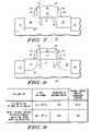
- FIGS. 1-8illustrate in cross-sectional form methods for making a semiconductor device in accordance with the present invention.
- FIG. 9illustrates in table form characteristics of a semiconductor device formed in accordance with the present invention as compared with a conventional device.
- FIG. 1illustrates a cross-sectional view of a semiconductor device 10 wherein a semiconductor substrate 12 is provided.
- the semiconductor substrate 12may be of various semiconductor materials such as single crystal silicon, gallium arsenide and other materials.
- an isolation trench 13 and an isolation trench 14for providing electrical isolation within the semiconductor substrate 12 .
- Overlying the semiconductor substrate 12is an insulating layer 16 .
- the insulating layer 16is an oxide such as silicon dioxide. Other dielectrics such as silicon oxynitride and high k dielectrics may be used.
- a control electrode or a gate 18Overlying the insulating layer 16 is a control electrode or a gate 18 . Both the gate 18 and the insulating layer 16 have been patterned in a conventional manner to overlie only a desired portion of the semiconductor substrate 12 .
- the gate 18is made of a conductive material such as polysilicon or metal, for example. Insulating layer 16 will therefore function as a gate oxide layer.
- FIG. 2illustrates a cross-sectional view of further processing of semiconductor device 10 .
- a blanket deposition of an insulating layer 20is then performed.
- the insulating layer 20is conformally deposited and therefore evenly forms on the sides of gate 18 as well as on exposed horizontal surfaces.
- insulating layer 20is made of silicon nitride. However, other dielectric materials may be used.
- FIG. 3illustrates in cross-sectional form further processing of semiconductor device 10 .
- An anisotropic etch of insulating layer 20is performed so that the insulating layer 20 is removed from all exposed horizontal surfaces but not at the exposed vertical surfaces. Therefore, insulating layer 20 remains along a continuous sidewall of the gate 18 and insulating layer 16 . It should be understood that two portions, a left-sided and a right-sided portion of the continuous sidewall are illustrated in the cross-sectional view.
- the etchwill remove a small portion (not shown) of the insulating layer 20 from the top of the sidewall but the effect is inconsequential.
- the etch chemistryis conventional and will therefore not be further discussed.
- a conventional extension ion implant with either P-conductivity or N-conductivity dopant materialis performed.
- a halo implantation(not shown) is done prior to the extension implantation.
- a halo implantationinvolves angled implanting in which ions are implant from two or more angles.
- the halo implantationmay be used to form a symmetric device having symmetric source/drain implantation or to form an asymmetric device having asymmetric source/drain implantation.
- the halo implantwill have an N-type conductivity.
- the halo implantwill have a P-type conductivity.
- the optional halo implantcontrols the short channel behavior of the semiconductor device 10 by compensating the extension dopant migration toward the channel region from the source and the drain.
- FIG. 4illustrates in cross-sectional form further processing of semiconductor device 10 wherein a source 22 and a drain 24 have been formed as a result of the ion implantation.
- An annealis performed to drive the implanted dopants under a portion of the gate 18 within the channel region.
- the temperature of the annealis typically in a range of nine hundred degrees Celsius to around eleven hundred degrees Celsius.
- the temperature of the anneal and the amount of time of the annealwill determine the amount that the implants are driven under the gate 18 . Therefore the length of the channel separation between source 22 and drain 24 may be controlled to avoid any short channel effects.
- FIG. 5illustrates in cross-sectional form further processing of semiconductor device 10 wherein a selective etch is performed to remove exposed portions of the source 22 and drain 24 .
- a conventional dry etchis used. In one form the dry etch is anisotropic. The etching results in a recessed region 26 where source 22 was previously present and a recessed region 28 wherein drain 24 was previously present. It should be noted also that some etching of the gate 18 occurs but that the amount of etching may typically be controlled through etch chemistry to avoid significant erosion of the gate 18 .
- a protecting cap layer(not shown) may first be deposited overlying gate 18 prior to the etching. With the presence of a cap layer, no etching of gate 18 would occur.
- the depth of the recessed regions 26 and 28is greater than the depth of source 22 and drain 24 , respectively.
- the depth of the recessionsmay vary, but should be large enough to totally remove the source 22 and the drain 24 .
- the depth of the recessed regions 26 and 28is within a range of approximately 300 Angstroms to 500 Angstroms.
- an important aspect of the etchingis that a portion of source 22 and a portion of drain 24 remain within semiconductor device 10 .
- a portion of source 22 underlying gate 18 and at an edge of the channel regionremains.
- a portion of drain 24 underlying gate 18 and at an opposite edge of the channel regionremains.
- FIG. 6Illustrated in FIG. 6 in cross-sectional form is further processing of semiconductor device 10 .
- the recessed regions 26 and 28are filled by a deposition with an epitaxial stressor material having insitu doping.
- the epitaxial stressor material for a P-channel transistoris silicon germanium having boron as the insitu dopant.
- the expitaxial stressor material for an N-channel transistoris silicon carbon having phosphorous as the insitu dopant. It can be seen from FIG. 6 and the following figures that the resulting dopant profile is very abrupt which is desired. The more abrupt the doping profile is, the better the device electrical performance becomes.
- a source region 30 and a drain region 32are therefore formed.
- a fill region 34is formed overlying gate 18 in the void created from the previous etching.
- the source region 30 and drain region 32are slightly elevated and have an upper surface that is planar with or higher than an upper surface of the insulating layer 16 . This elevation provides a margin for error to ensure that the upper surface of source region 30 and drain region 32 is at least above the lower surface of insulating layer 16 which functions as the gate dielectric for gate 18 .
- the source region 30 and the drain region 32 that contain stressor materialfunction to provide a significant amount of strain to the channel region due to the proximity of these regions to the channel. Additionally, without affecting the amount of strain, the separation distance between the source and the drain within the channel is independently controlled, largely as a function of an earlier anneal step. The resulting channel region has enhanced carrier mobility as a result of the increased channel strain.
- Fill region 34 and gate 18function together as a single conductive control electrode or gate for the semiconductor device 10 .
- the material that is used for both fill region 34 and gate 18is a conductor, but the two regions do not necessarily have to be of the same material.
- FIG. 7Illustrated in FIG. 7 is further processing of semiconductor device 10 wherein a completed functional transistor is formed.
- a sidewall liner 40 and a sidewall spacer 42are formed along all exposed side surfaces of the insulating layer 20 and over a portion of the source region 30 and the drain region 32 .
- the sidewall liner 40 and the sidewall spacer 42are formed by conventional deposition and etch techniques.
- a primary purpose for the sidewall liner 40 and sidewall spacer 42is to provide some offset from the gate stack for a silicided contact to each of the source region 30 and the drain region 32 .
- the sidewall liner 40functions with the sidewall spacer 42 to enhance the etching of the material used for these regions and permit accurate removal without degrading the upper surface of source region 30 and drain region 32 .
- the sidewall liner 40functions as an etch stop layer for the etching of sidewall spacer 42 material.
- the sidewall liner 40may then be readily removed with a selective wet etching processing.
- a single materialmay be used to form a sidewall spacer.
- the sidewall spacer 42is used to permit the formation of conductive contacts on the exposed upper surface of source region 30 , gate 34 and drain region 32 without directly electrically short circuiting these three elements.
- FIG. 8Illustrated in FIG. 8 is further processing of semiconductor device 10 wherein an alternative processing method is implemented. Assume again the structure of semiconductor device 10 in FIG. 5 . Instead of processing semiconductor device 10 as illustrated in FIGS. 6 and 7 , the semiconductor device 10 may be processed as illustrated in FIG. 8 .
- a hydrogen annealis performed when recessed regions 26 and 28 exist so that the profile of the semiconductor substrate 12 defining the recessed regions 26 and 28 is altered.
- the anneal that is performed in the presence of hydrogenmodifies the semiconductor substrate 12 by extending the silicon within the semiconductor substrate 12 and thereby making the contour of the recessed regions 26 and 28 rounded or curvilinear.
- the slope of the edge of drain region 32 measured with respect to a horizontal reference lineis represented by the angle ⁇ .
- the value of ⁇may vary but in one form is in a range of twenty degrees to seventy degrees.
- a typical anneal temperatureis, for example only, within a range of about 750 to 950 degrees Celsius for an amount of time of approximately one minute. However, if one processing parameter is varied, the other parameters may also differ. Either H 2 , hydrogen-containing agents, such as silane or germane, or a combination thereof may be used during the anneal.
- FIG. 9Illustrated in FIG. 9 is a table for illustrating benefits achieved regarding improved channel strain by using the methods described above.
- the source region 30 and the drain region 32have silicon germanium (SiGe) stressor material content in the form of approximately twenty-five percent germanium (Ge) and seventy-five percent silicon (Si). Silicon germanium is known to have the benefit of inducing strain when used in a source or drain. Comparisons will be made in FIG. 8 regarding the stress on a channel, the percentage actually achieved of a maximum one hundred percent of strain that is possible, and the channel carrier mobility enhancement that is achieved. For these three categories, a comparison between two significantly different methods is made.
- a silicon germanium deposition of stressor materialis followed by an ion implant of the stressor material to create source/drain extensions.
- an initial ion implantoccurs followed by the partial removal of the ion implanted regions and the deposition of insitu doped silicon germanium in the removed material areas.
- the second methodcorresponds to the methods described above in connection with FIGS. 1-8 .
- the stress on the channel when an implant is performed after the deposition of silicon germaniumis 150 ⁇ 10 6 Pascals (Pa).
- the implantis initially performed and the silicon germanium is deposited after partial removal thereof, the stress on the channel increases significantly to 500 ⁇ 10 6 Pascals.
- the realized percentage of the maximum strain that is achievableis thirty percent (30%). In contrast, when the implant is initially performed and the silicon germanium is deposited after partial removal thereof, the realized percentage of the maximum strain that is achievable is ninety-five percent (95%).
- the channel carrier mobility enhancement that is achievedis 10.5 percent. In contrast, when the implant is initially performed and the silicon germanium is deposited after partial removal thereof, the channel carrier mobility enhancement that is achieved is 35 percent. Therefore, it can be readily seen that a significant performance improvement in the amount of realized stress is achieved by using the methods described herein.
- a method for making a semiconductor deviceA semiconductor substrate is provided.
- a control electrode having a sidewall and overlying the semiconductor substrateis formed.
- An insulating layer adjacent the sidewall of the control electrodeis formed.
- the semiconductor substrate and the control electrodeare implanted to form first and second doped current electrode regions, a portion of each of the first and second doped current electrode regions being driven to underlie both the insulating layer and the control electrode in a channel region of the semiconductor device.
- the first and second doped current electrode regionsare removed from the semiconductor substrate except for underneath both the control electrode and the insulating layer to respectively form first and second trenches.
- An insitu doped material containing a different lattice constant relative to the semiconductor substrateis formed within the first and second trenches to fill the first and second trenches and function as first and second current electrodes of the semiconductor device, the first and second current electrodes applying a stress on the channel region.
- a hydrogen-containing gasis flowed over the semiconductor device at a temperature of at least six hundred degrees Celsius prior to forming the insitu doped material containing a different lattice constant relative to the semiconductor substrate, the hydrogen-containing gas modifying a slope of an edge of the first and second trenches to position the first and second trenches further away from the channel region.
- the slope of the edge of the first and second trenchesis modified by an angle measured relative to a horizontal reference that is within a range of twenty to seventy degrees.
- the insitu doped material containing a different lattice constant relative to the semiconductor substrateis formed by forming silicon germanium within the first and second trenches when the semiconductor device comprises a P conductivity channel region and forming silicon carbon within the first and second trenches when the semiconductor device comprises an N conductivity channel region.
- the insulating layer adjacent the sidewall of the control electrodeis formed by forming either silicon nitride or a composite material of silicon dioxide and silicon nitride.
- each of the first and second doped current electrode regionsis driven to underlie both the insulating layer and the control electrode in the channel region by annealing the semiconductor device at a temperature in a range of nine hundred degrees Celsius to eleven hundred degrees Celsius.
- a portion of the control electrodeis removed when removing the first and second doped current electrode regions and all of the removed portion is replaced with the insitu doped material containing a different lattice constant relative to the semiconductor substrate.
- a gateis formed having a sidewall and overlying the semiconductor substrate.
- a gate sidewall insulator adjacent the sidewall of the gateis formed.
- the semiconductor substrate and the gateare implanted to form first and second doped current electrode regions.
- the semiconductor substrateis annealed to move a portion of each of the first and second doped current electrode regions under the gate sidewall insulator and a portion of the gate in a channel region.
- the first and second doped current electrode regionsare removed from the semiconductor substrate except for underneath the portion of the gate and the gate sidewall insulator to respectively form first and second trenches.
- An insitu doped stressor materialis formed within the first and second trenches to fill the first and second trenches and function as first and second current electrodes, the first and second current electrode regions applying a stress on the channel region.
- a hydrogen-containing gasis flowed over the semiconductor substrate at a temperature of at least six hundred degrees Celsius prior to forming the insitu doped stressor material within the first and second trenches, the hydrogen-containing gas modifying a slope of an edge of the first and second trenches to position the first and second trenches further away from the channel region.
- the implantingfurther comprises performing both a halo implant and an extension implant to form the first and second doped current electrode regions.
- the halo implantis used to form asymmetric implantation of the first and second doped current electrode regions.
- a portion of the gateis removed when removing the first and second doped current electrode regions and subsequently replacing all removed portion with the insitu doped stressor material.
- a slope of a side of the first and second trenchesis modified by an angle measured relative to a horizontal reference that is within a range of twenty to seventy degrees.
- a first angleis used for the slope when the first and second trenches are P-conductivity type and a second angle is used for the slope when the first and second trenches are N-conductivity type, the first angle differing from the second angle. The variation depends upon short channel effect requirements.
- a method for making a transistor with strain enhancementcomprising sequential steps.
- a semiconductor substrateis provided.
- a gatehaving a sidewall and overlying the semiconductor substrate is formed.
- An insulating layer adjacent the sidewall of the gateis formed.
- the semiconductor substrate and the gateare implanted to form a source and a drain, a portion of each of the source and the drain being driven to underlie both the insulating layer and the gate in a channel region of the transistor underlying the gate.
- a portion of the source and drainis removed from the semiconductor substrate except for underneath both the gate and the insulating layer to respectively form first and second trenches.
- Insitu doped silicon germaniumis formed within the first and second trenches to fill the first and second trenches and function as the source and the drain of the transistor, the source and the drain applying a stress on the channel region.
- a hydrogen-containing gasis flowed over the transistor at a temperature of at least six hundred degrees Celsius after removing the portion of the source and drain but prior to forming insitu doped silicon germanium, the hydrogen-containing gas modifying a slope of an edge of the first and second trenches to position the first and second trenches further away from the channel region.
- the slope of the edge of the first and second trenchesis modified by an angle measured relative to a horizontal reference that is within a range of twenty to seventy degrees.
- a portion of the gateis removed when removing the source and drain and all of the removed portion is replaced with the insitu doped silicon germanium.
- both a halo implant and an extension implantare made to form the source and the drain.
- the halo implantis used to form asymmetric implantation of the source and the drain.
- the stress enhancement methodmay be used with a variety of stress-enhancing materials.
- the present inventionis not limited to the formation of transistors. It should be well understood that other devices, such as diodes and optical devices may benefit from the methods described herein. Accordingly, the specification and figures are to be regarded in an illustrative rather than a restrictive sense, and all such modifications are intended to be included within the scope of the present invention.
- pluralityis defined as two or more than two.
- anotheris defined as at least a second or more.
- the terms including and/or having, as used herein,are defined as comprising (i.e., open language).
Landscapes
- Insulated Gate Type Field-Effect Transistor (AREA)
Abstract
Description
Claims (15)
Priority Applications (1)
| Application Number | Priority Date | Filing Date | Title |
|---|---|---|---|
| US11/092,291US7282415B2 (en) | 2005-03-29 | 2005-03-29 | Method for making a semiconductor device with strain enhancement |
Applications Claiming Priority (1)
| Application Number | Priority Date | Filing Date | Title |
|---|---|---|---|
| US11/092,291US7282415B2 (en) | 2005-03-29 | 2005-03-29 | Method for making a semiconductor device with strain enhancement |
Publications (2)
| Publication Number | Publication Date |
|---|---|
| US20060228863A1 US20060228863A1 (en) | 2006-10-12 |
| US7282415B2true US7282415B2 (en) | 2007-10-16 |
Family
ID=37083648
Family Applications (1)
| Application Number | Title | Priority Date | Filing Date |
|---|---|---|---|
| US11/092,291Expired - Fee RelatedUS7282415B2 (en) | 2005-03-29 | 2005-03-29 | Method for making a semiconductor device with strain enhancement |
Country Status (1)
| Country | Link |
|---|---|
| US (1) | US7282415B2 (en) |
Cited By (10)
| Publication number | Priority date | Publication date | Assignee | Title |
|---|---|---|---|---|
| US20070020864A1 (en)* | 2005-07-16 | 2007-01-25 | Chartered Semiconductor Mfg | Method and structure to prevent silicide strapping of source/drain to body in semiconductor devices with source/drain stressor |
| US20080048217A1 (en)* | 2006-08-25 | 2008-02-28 | Samsung Electronics Co., Ltd. | Semiconductor device and method of fabricating the same |
| US20080153221A1 (en)* | 2006-12-20 | 2008-06-26 | Texas Instruments Incorporated | Use of a Single Mask During the Formation of a Transistor's Drain Extension and Recessed Strained Epi Regions |
| US20080265281A1 (en)* | 2005-05-10 | 2008-10-30 | International Business Machines Corporation | Embedded silicon germanium using a double buried oxide silicon-on-insulator wafer |
| US20090289280A1 (en)* | 2008-05-22 | 2009-11-26 | Da Zhang | Method for Making Transistors and the Device Thereof |
| US20100155898A1 (en)* | 2008-12-22 | 2010-06-24 | Varian Semiconductor Equipment Associates, Inc. | METHOD FOR ENHANCING TENSILE STRESS AND SOURCE/DRAIN ACTIVIATION USING Si:C |
| US7935593B2 (en) | 2009-02-05 | 2011-05-03 | Samsung Electronics Co., Ltd. | Stress optimization in dual embedded epitaxially grown semiconductor processing |
| US8003454B2 (en) | 2008-05-22 | 2011-08-23 | Freescale Semiconductor, Inc. | CMOS process with optimized PMOS and NMOS transistor devices |
| US20120119281A1 (en)* | 2010-11-16 | 2012-05-17 | Globalfoundries Singapore Pte. Ltd. | Integrated circuit system with bandgap material and method of manufacture thereof |
| US20150179742A1 (en)* | 2006-09-18 | 2015-06-25 | Pushkar Ranade | Active regions with compatible dielectric layers |
Families Citing this family (366)
| Publication number | Priority date | Publication date | Assignee | Title |
|---|---|---|---|---|
| US7902008B2 (en)* | 2005-08-03 | 2011-03-08 | Globalfoundries Inc. | Methods for fabricating a stressed MOS device |
| US8407634B1 (en) | 2005-12-01 | 2013-03-26 | Synopsys Inc. | Analysis of stress impact on transistor performance |
| US7560350B2 (en)* | 2006-04-17 | 2009-07-14 | United Microelectronics Corp. | Method for forming strained semiconductor device and method for forming source/drain region |
| EP1936696A1 (en)* | 2006-12-22 | 2008-06-25 | INTERUNIVERSITAIR MICROELEKTRONICA CENTRUM vzw (IMEC) | A field effect transistor device and methods of production thereof |
| EP1936697B1 (en)* | 2006-12-22 | 2016-03-09 | Imec | A field effect transistor device, and methods of production thereof |
| US7521314B2 (en)* | 2007-04-20 | 2009-04-21 | Freescale Semiconductor, Inc. | Method for selective removal of a layer |
| US7553717B2 (en)* | 2007-05-11 | 2009-06-30 | Texas Instruments Incorporated | Recess etch for epitaxial SiGe |
| US10378106B2 (en) | 2008-11-14 | 2019-08-13 | Asm Ip Holding B.V. | Method of forming insulation film by modified PEALD |
| US9394608B2 (en) | 2009-04-06 | 2016-07-19 | Asm America, Inc. | Semiconductor processing reactor and components thereof |
| US8802201B2 (en) | 2009-08-14 | 2014-08-12 | Asm America, Inc. | Systems and methods for thin-film deposition of metal oxides using excited nitrogen-oxygen species |
| JP2011054740A (en)* | 2009-09-01 | 2011-03-17 | Toshiba Corp | Semiconductor device and method of manufacturing the same |
| US8598003B2 (en) | 2009-12-21 | 2013-12-03 | Intel Corporation | Semiconductor device having doped epitaxial region and its methods of fabrication |
| US9312155B2 (en) | 2011-06-06 | 2016-04-12 | Asm Japan K.K. | High-throughput semiconductor-processing apparatus equipped with multiple dual-chamber modules |
| US10364496B2 (en) | 2011-06-27 | 2019-07-30 | Asm Ip Holding B.V. | Dual section module having shared and unshared mass flow controllers |
| US10854498B2 (en) | 2011-07-15 | 2020-12-01 | Asm Ip Holding B.V. | Wafer-supporting device and method for producing same |
| US20130023129A1 (en) | 2011-07-20 | 2013-01-24 | Asm America, Inc. | Pressure transmitter for a semiconductor processing environment |
| US9017481B1 (en) | 2011-10-28 | 2015-04-28 | Asm America, Inc. | Process feed management for semiconductor substrate processing |
| US9659799B2 (en) | 2012-08-28 | 2017-05-23 | Asm Ip Holding B.V. | Systems and methods for dynamic semiconductor process scheduling |
| US9190346B2 (en) | 2012-08-31 | 2015-11-17 | Synopsys, Inc. | Latch-up suppression and substrate noise coupling reduction through a substrate back-tie for 3D integrated circuits |
| US9817928B2 (en) | 2012-08-31 | 2017-11-14 | Synopsys, Inc. | Latch-up suppression and substrate noise coupling reduction through a substrate back-tie for 3D integrated circuits |
| US9021985B2 (en) | 2012-09-12 | 2015-05-05 | Asm Ip Holdings B.V. | Process gas management for an inductively-coupled plasma deposition reactor |
| US10714315B2 (en) | 2012-10-12 | 2020-07-14 | Asm Ip Holdings B.V. | Semiconductor reaction chamber showerhead |
| US9379018B2 (en) | 2012-12-17 | 2016-06-28 | Synopsys, Inc. | Increasing Ion/Ioff ratio in FinFETs and nano-wires |
| US8847324B2 (en) | 2012-12-17 | 2014-09-30 | Synopsys, Inc. | Increasing ION /IOFF ratio in FinFETs and nano-wires |
| US20160376700A1 (en) | 2013-02-01 | 2016-12-29 | Asm Ip Holding B.V. | System for treatment of deposition reactor |
| US9484191B2 (en) | 2013-03-08 | 2016-11-01 | Asm Ip Holding B.V. | Pulsed remote plasma method and system |
| US9589770B2 (en) | 2013-03-08 | 2017-03-07 | Asm Ip Holding B.V. | Method and systems for in-situ formation of intermediate reactive species |
| US9978650B2 (en)* | 2013-03-13 | 2018-05-22 | Taiwan Semiconductor Manufacturing Company, Ltd. | Transistor channel |
| US9240412B2 (en) | 2013-09-27 | 2016-01-19 | Asm Ip Holding B.V. | Semiconductor structure and device and methods of forming same using selective epitaxial process |
| US10683571B2 (en) | 2014-02-25 | 2020-06-16 | Asm Ip Holding B.V. | Gas supply manifold and method of supplying gases to chamber using same |
| US10167557B2 (en) | 2014-03-18 | 2019-01-01 | Asm Ip Holding B.V. | Gas distribution system, reactor including the system, and methods of using the same |
| US11015245B2 (en) | 2014-03-19 | 2021-05-25 | Asm Ip Holding B.V. | Gas-phase reactor and system having exhaust plenum and components thereof |
| US10858737B2 (en) | 2014-07-28 | 2020-12-08 | Asm Ip Holding B.V. | Showerhead assembly and components thereof |
| US9890456B2 (en) | 2014-08-21 | 2018-02-13 | Asm Ip Holding B.V. | Method and system for in situ formation of gas-phase compounds |
| US10941490B2 (en) | 2014-10-07 | 2021-03-09 | Asm Ip Holding B.V. | Multiple temperature range susceptor, assembly, reactor and system including the susceptor, and methods of using the same |
| US9657845B2 (en) | 2014-10-07 | 2017-05-23 | Asm Ip Holding B.V. | Variable conductance gas distribution apparatus and method |
| KR102263121B1 (en) | 2014-12-22 | 2021-06-09 | 에이에스엠 아이피 홀딩 비.브이. | Semiconductor device and manufacuring method thereof |
| US10529542B2 (en) | 2015-03-11 | 2020-01-07 | Asm Ip Holdings B.V. | Cross-flow reactor and method |
| US10276355B2 (en) | 2015-03-12 | 2019-04-30 | Asm Ip Holding B.V. | Multi-zone reactor, system including the reactor, and method of using the same |
| US10458018B2 (en) | 2015-06-26 | 2019-10-29 | Asm Ip Holding B.V. | Structures including metal carbide material, devices including the structures, and methods of forming same |
| US10600673B2 (en) | 2015-07-07 | 2020-03-24 | Asm Ip Holding B.V. | Magnetic susceptor to baseplate seal |
| US10083836B2 (en) | 2015-07-24 | 2018-09-25 | Asm Ip Holding B.V. | Formation of boron-doped titanium metal films with high work function |
| US9960072B2 (en) | 2015-09-29 | 2018-05-01 | Asm Ip Holding B.V. | Variable adjustment for precise matching of multiple chamber cavity housings |
| US10211308B2 (en) | 2015-10-21 | 2019-02-19 | Asm Ip Holding B.V. | NbMC layers |
| US10322384B2 (en) | 2015-11-09 | 2019-06-18 | Asm Ip Holding B.V. | Counter flow mixer for process chamber |
| US11139308B2 (en) | 2015-12-29 | 2021-10-05 | Asm Ip Holding B.V. | Atomic layer deposition of III-V compounds to form V-NAND devices |
| US10468251B2 (en) | 2016-02-19 | 2019-11-05 | Asm Ip Holding B.V. | Method for forming spacers using silicon nitride film for spacer-defined multiple patterning |
| US10529554B2 (en) | 2016-02-19 | 2020-01-07 | Asm Ip Holding B.V. | Method for forming silicon nitride film selectively on sidewalls or flat surfaces of trenches |
| US10501866B2 (en) | 2016-03-09 | 2019-12-10 | Asm Ip Holding B.V. | Gas distribution apparatus for improved film uniformity in an epitaxial system |
| US10343920B2 (en) | 2016-03-18 | 2019-07-09 | Asm Ip Holding B.V. | Aligned carbon nanotubes |
| US9892913B2 (en) | 2016-03-24 | 2018-02-13 | Asm Ip Holding B.V. | Radial and thickness control via biased multi-port injection settings |
| US10865475B2 (en) | 2016-04-21 | 2020-12-15 | Asm Ip Holding B.V. | Deposition of metal borides and silicides |
| US10190213B2 (en) | 2016-04-21 | 2019-01-29 | Asm Ip Holding B.V. | Deposition of metal borides |
| US10367080B2 (en) | 2016-05-02 | 2019-07-30 | Asm Ip Holding B.V. | Method of forming a germanium oxynitride film |
| US10032628B2 (en)* | 2016-05-02 | 2018-07-24 | Asm Ip Holding B.V. | Source/drain performance through conformal solid state doping |
| KR102592471B1 (en) | 2016-05-17 | 2023-10-20 | 에이에스엠 아이피 홀딩 비.브이. | Method of forming metal interconnection and method of fabricating semiconductor device using the same |
| US11453943B2 (en) | 2016-05-25 | 2022-09-27 | Asm Ip Holding B.V. | Method for forming carbon-containing silicon/metal oxide or nitride film by ALD using silicon precursor and hydrocarbon precursor |
| US10388509B2 (en) | 2016-06-28 | 2019-08-20 | Asm Ip Holding B.V. | Formation of epitaxial layers via dislocation filtering |
| US9859151B1 (en) | 2016-07-08 | 2018-01-02 | Asm Ip Holding B.V. | Selective film deposition method to form air gaps |
| US10612137B2 (en) | 2016-07-08 | 2020-04-07 | Asm Ip Holdings B.V. | Organic reactants for atomic layer deposition |
| US10714385B2 (en) | 2016-07-19 | 2020-07-14 | Asm Ip Holding B.V. | Selective deposition of tungsten |
| KR102354490B1 (en) | 2016-07-27 | 2022-01-21 | 에이에스엠 아이피 홀딩 비.브이. | Method of processing a substrate |
| US10395919B2 (en) | 2016-07-28 | 2019-08-27 | Asm Ip Holding B.V. | Method and apparatus for filling a gap |
| KR102532607B1 (en) | 2016-07-28 | 2023-05-15 | 에이에스엠 아이피 홀딩 비.브이. | Substrate processing apparatus and method of operating the same |
| US9887082B1 (en) | 2016-07-28 | 2018-02-06 | Asm Ip Holding B.V. | Method and apparatus for filling a gap |
| US9812320B1 (en) | 2016-07-28 | 2017-11-07 | Asm Ip Holding B.V. | Method and apparatus for filling a gap |
| US10410943B2 (en) | 2016-10-13 | 2019-09-10 | Asm Ip Holding B.V. | Method for passivating a surface of a semiconductor and related systems |
| US10643826B2 (en) | 2016-10-26 | 2020-05-05 | Asm Ip Holdings B.V. | Methods for thermally calibrating reaction chambers |
| US11532757B2 (en) | 2016-10-27 | 2022-12-20 | Asm Ip Holding B.V. | Deposition of charge trapping layers |
| US10435790B2 (en) | 2016-11-01 | 2019-10-08 | Asm Ip Holding B.V. | Method of subatmospheric plasma-enhanced ALD using capacitively coupled electrodes with narrow gap |
| US10643904B2 (en) | 2016-11-01 | 2020-05-05 | Asm Ip Holdings B.V. | Methods for forming a semiconductor device and related semiconductor device structures |
| US10714350B2 (en) | 2016-11-01 | 2020-07-14 | ASM IP Holdings, B.V. | Methods for forming a transition metal niobium nitride film on a substrate by atomic layer deposition and related semiconductor device structures |
| US10229833B2 (en) | 2016-11-01 | 2019-03-12 | Asm Ip Holding B.V. | Methods for forming a transition metal nitride film on a substrate by atomic layer deposition and related semiconductor device structures |
| US10134757B2 (en) | 2016-11-07 | 2018-11-20 | Asm Ip Holding B.V. | Method of processing a substrate and a device manufactured by using the method |
| KR102546317B1 (en) | 2016-11-15 | 2023-06-21 | 에이에스엠 아이피 홀딩 비.브이. | Gas supply unit and substrate processing apparatus including the same |
| US10340135B2 (en) | 2016-11-28 | 2019-07-02 | Asm Ip Holding B.V. | Method of topologically restricted plasma-enhanced cyclic deposition of silicon or metal nitride |
| KR102762543B1 (en) | 2016-12-14 | 2025-02-05 | 에이에스엠 아이피 홀딩 비.브이. | Substrate processing apparatus |
| US11447861B2 (en) | 2016-12-15 | 2022-09-20 | Asm Ip Holding B.V. | Sequential infiltration synthesis apparatus and a method of forming a patterned structure |
| US11581186B2 (en) | 2016-12-15 | 2023-02-14 | Asm Ip Holding B.V. | Sequential infiltration synthesis apparatus |
| KR102700194B1 (en) | 2016-12-19 | 2024-08-28 | 에이에스엠 아이피 홀딩 비.브이. | Substrate processing apparatus |
| US10269558B2 (en) | 2016-12-22 | 2019-04-23 | Asm Ip Holding B.V. | Method of forming a structure on a substrate |
| US10867788B2 (en) | 2016-12-28 | 2020-12-15 | Asm Ip Holding B.V. | Method of forming a structure on a substrate |
| US11390950B2 (en) | 2017-01-10 | 2022-07-19 | Asm Ip Holding B.V. | Reactor system and method to reduce residue buildup during a film deposition process |
| US10655221B2 (en) | 2017-02-09 | 2020-05-19 | Asm Ip Holding B.V. | Method for depositing oxide film by thermal ALD and PEALD |
| US10468261B2 (en) | 2017-02-15 | 2019-11-05 | Asm Ip Holding B.V. | Methods for forming a metallic film on a substrate by cyclical deposition and related semiconductor device structures |
| US10529563B2 (en) | 2017-03-29 | 2020-01-07 | Asm Ip Holdings B.V. | Method for forming doped metal oxide films on a substrate by cyclical deposition and related semiconductor device structures |
| US10283353B2 (en) | 2017-03-29 | 2019-05-07 | Asm Ip Holding B.V. | Method of reforming insulating film deposited on substrate with recess pattern |
| KR102457289B1 (en) | 2017-04-25 | 2022-10-21 | 에이에스엠 아이피 홀딩 비.브이. | Method for depositing a thin film and manufacturing a semiconductor device |
| US10446393B2 (en) | 2017-05-08 | 2019-10-15 | Asm Ip Holding B.V. | Methods for forming silicon-containing epitaxial layers and related semiconductor device structures |
| US10770286B2 (en) | 2017-05-08 | 2020-09-08 | Asm Ip Holdings B.V. | Methods for selectively forming a silicon nitride film on a substrate and related semiconductor device structures |
| US10892156B2 (en) | 2017-05-08 | 2021-01-12 | Asm Ip Holding B.V. | Methods for forming a silicon nitride film on a substrate and related semiconductor device structures |
| US10504742B2 (en) | 2017-05-31 | 2019-12-10 | Asm Ip Holding B.V. | Method of atomic layer etching using hydrogen plasma |
| US10886123B2 (en) | 2017-06-02 | 2021-01-05 | Asm Ip Holding B.V. | Methods for forming low temperature semiconductor layers and related semiconductor device structures |
| US12040200B2 (en) | 2017-06-20 | 2024-07-16 | Asm Ip Holding B.V. | Semiconductor processing apparatus and methods for calibrating a semiconductor processing apparatus |
| US11306395B2 (en) | 2017-06-28 | 2022-04-19 | Asm Ip Holding B.V. | Methods for depositing a transition metal nitride film on a substrate by atomic layer deposition and related deposition apparatus |
| US10685834B2 (en) | 2017-07-05 | 2020-06-16 | Asm Ip Holdings B.V. | Methods for forming a silicon germanium tin layer and related semiconductor device structures |
| KR20190009245A (en) | 2017-07-18 | 2019-01-28 | 에이에스엠 아이피 홀딩 비.브이. | Methods for forming a semiconductor device structure and related semiconductor device structures |
| US10541333B2 (en) | 2017-07-19 | 2020-01-21 | Asm Ip Holding B.V. | Method for depositing a group IV semiconductor and related semiconductor device structures |
| US11018002B2 (en) | 2017-07-19 | 2021-05-25 | Asm Ip Holding B.V. | Method for selectively depositing a Group IV semiconductor and related semiconductor device structures |
| US11374112B2 (en) | 2017-07-19 | 2022-06-28 | Asm Ip Holding B.V. | Method for depositing a group IV semiconductor and related semiconductor device structures |
| US10605530B2 (en) | 2017-07-26 | 2020-03-31 | Asm Ip Holding B.V. | Assembly of a liner and a flange for a vertical furnace as well as the liner and the vertical furnace |
| US10312055B2 (en) | 2017-07-26 | 2019-06-04 | Asm Ip Holding B.V. | Method of depositing film by PEALD using negative bias |
| US10590535B2 (en) | 2017-07-26 | 2020-03-17 | Asm Ip Holdings B.V. | Chemical treatment, deposition and/or infiltration apparatus and method for using the same |
| TWI815813B (en) | 2017-08-04 | 2023-09-21 | 荷蘭商Asm智慧財產控股公司 | Showerhead assembly for distributing a gas within a reaction chamber |
| US10692741B2 (en) | 2017-08-08 | 2020-06-23 | Asm Ip Holdings B.V. | Radiation shield |
| US10770336B2 (en) | 2017-08-08 | 2020-09-08 | Asm Ip Holding B.V. | Substrate lift mechanism and reactor including same |
| US11769682B2 (en) | 2017-08-09 | 2023-09-26 | Asm Ip Holding B.V. | Storage apparatus for storing cassettes for substrates and processing apparatus equipped therewith |
| US10249524B2 (en) | 2017-08-09 | 2019-04-02 | Asm Ip Holding B.V. | Cassette holder assembly for a substrate cassette and holding member for use in such assembly |
| US11139191B2 (en) | 2017-08-09 | 2021-10-05 | Asm Ip Holding B.V. | Storage apparatus for storing cassettes for substrates and processing apparatus equipped therewith |
| US10236177B1 (en) | 2017-08-22 | 2019-03-19 | ASM IP Holding B.V.. | Methods for depositing a doped germanium tin semiconductor and related semiconductor device structures |
| USD900036S1 (en) | 2017-08-24 | 2020-10-27 | Asm Ip Holding B.V. | Heater electrical connector and adapter |
| US11830730B2 (en) | 2017-08-29 | 2023-11-28 | Asm Ip Holding B.V. | Layer forming method and apparatus |
| KR102491945B1 (en) | 2017-08-30 | 2023-01-26 | 에이에스엠 아이피 홀딩 비.브이. | Substrate processing apparatus |
| US11295980B2 (en) | 2017-08-30 | 2022-04-05 | Asm Ip Holding B.V. | Methods for depositing a molybdenum metal film over a dielectric surface of a substrate by a cyclical deposition process and related semiconductor device structures |
| US11056344B2 (en) | 2017-08-30 | 2021-07-06 | Asm Ip Holding B.V. | Layer forming method |
| KR102401446B1 (en) | 2017-08-31 | 2022-05-24 | 에이에스엠 아이피 홀딩 비.브이. | Substrate processing apparatus |
| US10607895B2 (en) | 2017-09-18 | 2020-03-31 | Asm Ip Holdings B.V. | Method for forming a semiconductor device structure comprising a gate fill metal |
| KR102630301B1 (en) | 2017-09-21 | 2024-01-29 | 에이에스엠 아이피 홀딩 비.브이. | Method of sequential infiltration synthesis treatment of infiltrateable material and structures and devices formed using same |
| US10844484B2 (en) | 2017-09-22 | 2020-11-24 | Asm Ip Holding B.V. | Apparatus for dispensing a vapor phase reactant to a reaction chamber and related methods |
| US10658205B2 (en) | 2017-09-28 | 2020-05-19 | Asm Ip Holdings B.V. | Chemical dispensing apparatus and methods for dispensing a chemical to a reaction chamber |
| US10403504B2 (en) | 2017-10-05 | 2019-09-03 | Asm Ip Holding B.V. | Method for selectively depositing a metallic film on a substrate |
| US10319588B2 (en) | 2017-10-10 | 2019-06-11 | Asm Ip Holding B.V. | Method for depositing a metal chalcogenide on a substrate by cyclical deposition |
| US10923344B2 (en) | 2017-10-30 | 2021-02-16 | Asm Ip Holding B.V. | Methods for forming a semiconductor structure and related semiconductor structures |
| KR102443047B1 (en) | 2017-11-16 | 2022-09-14 | 에이에스엠 아이피 홀딩 비.브이. | Method of processing a substrate and a device manufactured by the same |
| US10910262B2 (en) | 2017-11-16 | 2021-02-02 | Asm Ip Holding B.V. | Method of selectively depositing a capping layer structure on a semiconductor device structure |
| US11022879B2 (en) | 2017-11-24 | 2021-06-01 | Asm Ip Holding B.V. | Method of forming an enhanced unexposed photoresist layer |
| CN111344522B (en) | 2017-11-27 | 2022-04-12 | 阿斯莫Ip控股公司 | Including clean mini-environment device |
| WO2019103613A1 (en) | 2017-11-27 | 2019-05-31 | Asm Ip Holding B.V. | A storage device for storing wafer cassettes for use with a batch furnace |
| US10290508B1 (en) | 2017-12-05 | 2019-05-14 | Asm Ip Holding B.V. | Method for forming vertical spacers for spacer-defined patterning |
| US10872771B2 (en) | 2018-01-16 | 2020-12-22 | Asm Ip Holding B. V. | Method for depositing a material film on a substrate within a reaction chamber by a cyclical deposition process and related device structures |
| TWI799494B (en) | 2018-01-19 | 2023-04-21 | 荷蘭商Asm 智慧財產控股公司 | Deposition method |
| KR102695659B1 (en) | 2018-01-19 | 2024-08-14 | 에이에스엠 아이피 홀딩 비.브이. | Method for depositing a gap filling layer by plasma assisted deposition |
| USD903477S1 (en) | 2018-01-24 | 2020-12-01 | Asm Ip Holdings B.V. | Metal clamp |
| US11018047B2 (en) | 2018-01-25 | 2021-05-25 | Asm Ip Holding B.V. | Hybrid lift pin |
| USD880437S1 (en) | 2018-02-01 | 2020-04-07 | Asm Ip Holding B.V. | Gas supply plate for semiconductor manufacturing apparatus |
| US10535516B2 (en) | 2018-02-01 | 2020-01-14 | Asm Ip Holdings B.V. | Method for depositing a semiconductor structure on a surface of a substrate and related semiconductor structures |
| US11081345B2 (en) | 2018-02-06 | 2021-08-03 | Asm Ip Holding B.V. | Method of post-deposition treatment for silicon oxide film |
| WO2019158960A1 (en) | 2018-02-14 | 2019-08-22 | Asm Ip Holding B.V. | A method for depositing a ruthenium-containing film on a substrate by a cyclical deposition process |
| US10896820B2 (en) | 2018-02-14 | 2021-01-19 | Asm Ip Holding B.V. | Method for depositing a ruthenium-containing film on a substrate by a cyclical deposition process |
| US10731249B2 (en) | 2018-02-15 | 2020-08-04 | Asm Ip Holding B.V. | Method of forming a transition metal containing film on a substrate by a cyclical deposition process, a method for supplying a transition metal halide compound to a reaction chamber, and related vapor deposition apparatus |
| KR102636427B1 (en) | 2018-02-20 | 2024-02-13 | 에이에스엠 아이피 홀딩 비.브이. | Substrate processing method and apparatus |
| US10658181B2 (en) | 2018-02-20 | 2020-05-19 | Asm Ip Holding B.V. | Method of spacer-defined direct patterning in semiconductor fabrication |
| US10975470B2 (en) | 2018-02-23 | 2021-04-13 | Asm Ip Holding B.V. | Apparatus for detecting or monitoring for a chemical precursor in a high temperature environment |
| US11473195B2 (en) | 2018-03-01 | 2022-10-18 | Asm Ip Holding B.V. | Semiconductor processing apparatus and a method for processing a substrate |
| US11629406B2 (en) | 2018-03-09 | 2023-04-18 | Asm Ip Holding B.V. | Semiconductor processing apparatus comprising one or more pyrometers for measuring a temperature of a substrate during transfer of the substrate |
| US11114283B2 (en) | 2018-03-16 | 2021-09-07 | Asm Ip Holding B.V. | Reactor, system including the reactor, and methods of manufacturing and using same |
| KR102646467B1 (en) | 2018-03-27 | 2024-03-11 | 에이에스엠 아이피 홀딩 비.브이. | Method of forming an electrode on a substrate and a semiconductor device structure including an electrode |
| US10510536B2 (en) | 2018-03-29 | 2019-12-17 | Asm Ip Holding B.V. | Method of depositing a co-doped polysilicon film on a surface of a substrate within a reaction chamber |
| US11230766B2 (en) | 2018-03-29 | 2022-01-25 | Asm Ip Holding B.V. | Substrate processing apparatus and method |
| US11088002B2 (en) | 2018-03-29 | 2021-08-10 | Asm Ip Holding B.V. | Substrate rack and a substrate processing system and method |
| KR102501472B1 (en) | 2018-03-30 | 2023-02-20 | 에이에스엠 아이피 홀딩 비.브이. | Substrate processing method |
| KR102600229B1 (en) | 2018-04-09 | 2023-11-10 | 에이에스엠 아이피 홀딩 비.브이. | Substrate supporting device, substrate processing apparatus including the same and substrate processing method |
| TWI811348B (en) | 2018-05-08 | 2023-08-11 | 荷蘭商Asm 智慧財產控股公司 | Methods for depositing an oxide film on a substrate by a cyclical deposition process and related device structures |
| US12025484B2 (en) | 2018-05-08 | 2024-07-02 | Asm Ip Holding B.V. | Thin film forming method |
| US12272527B2 (en) | 2018-05-09 | 2025-04-08 | Asm Ip Holding B.V. | Apparatus for use with hydrogen radicals and method of using same |
| KR20190129718A (en) | 2018-05-11 | 2019-11-20 | 에이에스엠 아이피 홀딩 비.브이. | Methods for forming a doped metal carbide film on a substrate and related semiconductor device structures |
| KR102596988B1 (en) | 2018-05-28 | 2023-10-31 | 에이에스엠 아이피 홀딩 비.브이. | Method of processing a substrate and a device manufactured by the same |
| US11718913B2 (en) | 2018-06-04 | 2023-08-08 | Asm Ip Holding B.V. | Gas distribution system and reactor system including same |
| TWI840362B (en) | 2018-06-04 | 2024-05-01 | 荷蘭商Asm Ip私人控股有限公司 | Wafer handling chamber with moisture reduction |
| US11286562B2 (en) | 2018-06-08 | 2022-03-29 | Asm Ip Holding B.V. | Gas-phase chemical reactor and method of using same |
| KR102568797B1 (en) | 2018-06-21 | 2023-08-21 | 에이에스엠 아이피 홀딩 비.브이. | Substrate processing system |
| US10797133B2 (en) | 2018-06-21 | 2020-10-06 | Asm Ip Holding B.V. | Method for depositing a phosphorus doped silicon arsenide film and related semiconductor device structures |
| TWI873894B (en) | 2018-06-27 | 2025-02-21 | 荷蘭商Asm Ip私人控股有限公司 | Cyclic deposition methods for forming metal-containing material and films and structures including the metal-containing material |
| KR102854019B1 (en) | 2018-06-27 | 2025-09-02 | 에이에스엠 아이피 홀딩 비.브이. | Periodic deposition method for forming a metal-containing material and films and structures comprising the metal-containing material |
| KR102686758B1 (en) | 2018-06-29 | 2024-07-18 | 에이에스엠 아이피 홀딩 비.브이. | Method for depositing a thin film and manufacturing a semiconductor device |
| US10612136B2 (en) | 2018-06-29 | 2020-04-07 | ASM IP Holding, B.V. | Temperature-controlled flange and reactor system including same |
| US10388513B1 (en) | 2018-07-03 | 2019-08-20 | Asm Ip Holding B.V. | Method for depositing silicon-free carbon-containing film as gap-fill layer by pulse plasma-assisted deposition |
| US10755922B2 (en) | 2018-07-03 | 2020-08-25 | Asm Ip Holding B.V. | Method for depositing silicon-free carbon-containing film as gap-fill layer by pulse plasma-assisted deposition |
| US10767789B2 (en) | 2018-07-16 | 2020-09-08 | Asm Ip Holding B.V. | Diaphragm valves, valve components, and methods for forming valve components |
| US10483099B1 (en) | 2018-07-26 | 2019-11-19 | Asm Ip Holding B.V. | Method for forming thermally stable organosilicon polymer film |
| US11053591B2 (en) | 2018-08-06 | 2021-07-06 | Asm Ip Holding B.V. | Multi-port gas injection system and reactor system including same |
| US10883175B2 (en) | 2018-08-09 | 2021-01-05 | Asm Ip Holding B.V. | Vertical furnace for processing substrates and a liner for use therein |
| US10829852B2 (en) | 2018-08-16 | 2020-11-10 | Asm Ip Holding B.V. | Gas distribution device for a wafer processing apparatus |
| US11430674B2 (en) | 2018-08-22 | 2022-08-30 | Asm Ip Holding B.V. | Sensor array, apparatus for dispensing a vapor phase reactant to a reaction chamber and related methods |
| US11024523B2 (en) | 2018-09-11 | 2021-06-01 | Asm Ip Holding B.V. | Substrate processing apparatus and method |
| KR102707956B1 (en) | 2018-09-11 | 2024-09-19 | 에이에스엠 아이피 홀딩 비.브이. | Method for deposition of a thin film |
| US11049751B2 (en) | 2018-09-14 | 2021-06-29 | Asm Ip Holding B.V. | Cassette supply system to store and handle cassettes and processing apparatus equipped therewith |
| CN110970344B (en) | 2018-10-01 | 2024-10-25 | Asmip控股有限公司 | Substrate holding apparatus, system comprising the same and method of using the same |
| US11232963B2 (en) | 2018-10-03 | 2022-01-25 | Asm Ip Holding B.V. | Substrate processing apparatus and method |
| KR102592699B1 (en) | 2018-10-08 | 2023-10-23 | 에이에스엠 아이피 홀딩 비.브이. | Substrate support unit and apparatuses for depositing thin film and processing the substrate including the same |
| US10847365B2 (en) | 2018-10-11 | 2020-11-24 | Asm Ip Holding B.V. | Method of forming conformal silicon carbide film by cyclic CVD |
| US10811256B2 (en) | 2018-10-16 | 2020-10-20 | Asm Ip Holding B.V. | Method for etching a carbon-containing feature |
| KR102546322B1 (en) | 2018-10-19 | 2023-06-21 | 에이에스엠 아이피 홀딩 비.브이. | Substrate processing apparatus and substrate processing method |
| KR102605121B1 (en) | 2018-10-19 | 2023-11-23 | 에이에스엠 아이피 홀딩 비.브이. | Substrate processing apparatus and substrate processing method |
| USD948463S1 (en) | 2018-10-24 | 2022-04-12 | Asm Ip Holding B.V. | Susceptor for semiconductor substrate supporting apparatus |
| US10381219B1 (en) | 2018-10-25 | 2019-08-13 | Asm Ip Holding B.V. | Methods for forming a silicon nitride film |
| US12378665B2 (en) | 2018-10-26 | 2025-08-05 | Asm Ip Holding B.V. | High temperature coatings for a preclean and etch apparatus and related methods |
| US11087997B2 (en) | 2018-10-31 | 2021-08-10 | Asm Ip Holding B.V. | Substrate processing apparatus for processing substrates |
| KR102748291B1 (en) | 2018-11-02 | 2024-12-31 | 에이에스엠 아이피 홀딩 비.브이. | Substrate support unit and substrate processing apparatus including the same |
| US11572620B2 (en) | 2018-11-06 | 2023-02-07 | Asm Ip Holding B.V. | Methods for selectively depositing an amorphous silicon film on a substrate |
| US11031242B2 (en) | 2018-11-07 | 2021-06-08 | Asm Ip Holding B.V. | Methods for depositing a boron doped silicon germanium film |
| US10847366B2 (en) | 2018-11-16 | 2020-11-24 | Asm Ip Holding B.V. | Methods for depositing a transition metal chalcogenide film on a substrate by a cyclical deposition process |
| US10818758B2 (en) | 2018-11-16 | 2020-10-27 | Asm Ip Holding B.V. | Methods for forming a metal silicate film on a substrate in a reaction chamber and related semiconductor device structures |
| US10559458B1 (en) | 2018-11-26 | 2020-02-11 | Asm Ip Holding B.V. | Method of forming oxynitride film |
| US12040199B2 (en) | 2018-11-28 | 2024-07-16 | Asm Ip Holding B.V. | Substrate processing apparatus for processing substrates |
| US11217444B2 (en) | 2018-11-30 | 2022-01-04 | Asm Ip Holding B.V. | Method for forming an ultraviolet radiation responsive metal oxide-containing film |
| KR102636428B1 (en) | 2018-12-04 | 2024-02-13 | 에이에스엠 아이피 홀딩 비.브이. | A method for cleaning a substrate processing apparatus |
| US11158513B2 (en) | 2018-12-13 | 2021-10-26 | Asm Ip Holding B.V. | Methods for forming a rhenium-containing film on a substrate by a cyclical deposition process and related semiconductor device structures |
| TWI874340B (en) | 2018-12-14 | 2025-03-01 | 荷蘭商Asm Ip私人控股有限公司 | Method of forming device structure, structure formed by the method and system for performing the method |
| TWI866480B (en) | 2019-01-17 | 2024-12-11 | 荷蘭商Asm Ip 私人控股有限公司 | Methods of forming a transition metal containing film on a substrate by a cyclical deposition process |
| KR102727227B1 (en) | 2019-01-22 | 2024-11-07 | 에이에스엠 아이피 홀딩 비.브이. | Semiconductor processing device |
| CN111524788B (en) | 2019-02-01 | 2023-11-24 | Asm Ip私人控股有限公司 | Method for forming topologically selective films of silicon oxide |
| TWI873122B (en) | 2019-02-20 | 2025-02-21 | 荷蘭商Asm Ip私人控股有限公司 | Method of filling a recess formed within a surface of a substrate, semiconductor structure formed according to the method, and semiconductor processing apparatus |
| TWI838458B (en) | 2019-02-20 | 2024-04-11 | 荷蘭商Asm Ip私人控股有限公司 | Apparatus and methods for plug fill deposition in 3-d nand applications |
| TWI845607B (en) | 2019-02-20 | 2024-06-21 | 荷蘭商Asm Ip私人控股有限公司 | Cyclical deposition method and apparatus for filling a recess formed within a substrate surface |
| KR102626263B1 (en) | 2019-02-20 | 2024-01-16 | 에이에스엠 아이피 홀딩 비.브이. | Cyclical deposition method including treatment step and apparatus for same |
| TWI842826B (en) | 2019-02-22 | 2024-05-21 | 荷蘭商Asm Ip私人控股有限公司 | Substrate processing apparatus and method for processing substrate |
| US11742198B2 (en) | 2019-03-08 | 2023-08-29 | Asm Ip Holding B.V. | Structure including SiOCN layer and method of forming same |
| KR102782593B1 (en) | 2019-03-08 | 2025-03-14 | 에이에스엠 아이피 홀딩 비.브이. | Structure Including SiOC Layer and Method of Forming Same |
| KR102858005B1 (en) | 2019-03-08 | 2025-09-09 | 에이에스엠 아이피 홀딩 비.브이. | Method for Selective Deposition of Silicon Nitride Layer and Structure Including Selectively-Deposited Silicon Nitride Layer |
| JP2020167398A (en) | 2019-03-28 | 2020-10-08 | エーエスエム・アイピー・ホールディング・ベー・フェー | Door openers and substrate processing equipment provided with door openers |
| KR102809999B1 (en) | 2019-04-01 | 2025-05-19 | 에이에스엠 아이피 홀딩 비.브이. | Method of manufacturing semiconductor device |
| KR20200123380A (en) | 2019-04-19 | 2020-10-29 | 에이에스엠 아이피 홀딩 비.브이. | Layer forming method and apparatus |
| KR20200125453A (en) | 2019-04-24 | 2020-11-04 | 에이에스엠 아이피 홀딩 비.브이. | Gas-phase reactor system and method of using same |
| KR20200130121A (en) | 2019-05-07 | 2020-11-18 | 에이에스엠 아이피 홀딩 비.브이. | Chemical source vessel with dip tube |
| US11289326B2 (en) | 2019-05-07 | 2022-03-29 | Asm Ip Holding B.V. | Method for reforming amorphous carbon polymer film |
| KR20200130652A (en) | 2019-05-10 | 2020-11-19 | 에이에스엠 아이피 홀딩 비.브이. | Method of depositing material onto a surface and structure formed according to the method |
| JP7612342B2 (en) | 2019-05-16 | 2025-01-14 | エーエスエム・アイピー・ホールディング・ベー・フェー | Wafer boat handling apparatus, vertical batch furnace and method |
| JP7598201B2 (en) | 2019-05-16 | 2024-12-11 | エーエスエム・アイピー・ホールディング・ベー・フェー | Wafer boat handling apparatus, vertical batch furnace and method |
| USD947913S1 (en) | 2019-05-17 | 2022-04-05 | Asm Ip Holding B.V. | Susceptor shaft |
| USD975665S1 (en) | 2019-05-17 | 2023-01-17 | Asm Ip Holding B.V. | Susceptor shaft |
| USD935572S1 (en) | 2019-05-24 | 2021-11-09 | Asm Ip Holding B.V. | Gas channel plate |
| USD922229S1 (en) | 2019-06-05 | 2021-06-15 | Asm Ip Holding B.V. | Device for controlling a temperature of a gas supply unit |
| KR20200141002A (en) | 2019-06-06 | 2020-12-17 | 에이에스엠 아이피 홀딩 비.브이. | Method of using a gas-phase reactor system including analyzing exhausted gas |
| KR20200141931A (en) | 2019-06-10 | 2020-12-21 | 에이에스엠 아이피 홀딩 비.브이. | Method for cleaning quartz epitaxial chambers |
| KR20200143254A (en) | 2019-06-11 | 2020-12-23 | 에이에스엠 아이피 홀딩 비.브이. | Method of forming an electronic structure using an reforming gas, system for performing the method, and structure formed using the method |
| USD944946S1 (en) | 2019-06-14 | 2022-03-01 | Asm Ip Holding B.V. | Shower plate |
| USD931978S1 (en) | 2019-06-27 | 2021-09-28 | Asm Ip Holding B.V. | Showerhead vacuum transport |
| KR20210005515A (en) | 2019-07-03 | 2021-01-14 | 에이에스엠 아이피 홀딩 비.브이. | Temperature control assembly for substrate processing apparatus and method of using same |
| JP7499079B2 (en) | 2019-07-09 | 2024-06-13 | エーエスエム・アイピー・ホールディング・ベー・フェー | Plasma device using coaxial waveguide and substrate processing method |
| CN112216646A (en) | 2019-07-10 | 2021-01-12 | Asm Ip私人控股有限公司 | Substrate supporting assembly and substrate processing device comprising same |
| KR20210010307A (en) | 2019-07-16 | 2021-01-27 | 에이에스엠 아이피 홀딩 비.브이. | Substrate processing apparatus |
| KR20210010816A (en) | 2019-07-17 | 2021-01-28 | 에이에스엠 아이피 홀딩 비.브이. | Radical assist ignition plasma system and method |
| KR102860110B1 (en) | 2019-07-17 | 2025-09-16 | 에이에스엠 아이피 홀딩 비.브이. | Methods of forming silicon germanium structures |
| US11643724B2 (en) | 2019-07-18 | 2023-05-09 | Asm Ip Holding B.V. | Method of forming structures using a neutral beam |
| TWI839544B (en) | 2019-07-19 | 2024-04-21 | 荷蘭商Asm Ip私人控股有限公司 | Method of forming topology-controlled amorphous carbon polymer film |
| KR20210010817A (en) | 2019-07-19 | 2021-01-28 | 에이에스엠 아이피 홀딩 비.브이. | Method of Forming Topology-Controlled Amorphous Carbon Polymer Film |
| TWI851767B (en) | 2019-07-29 | 2024-08-11 | 荷蘭商Asm Ip私人控股有限公司 | Methods for selective deposition utilizing n-type dopants and/or alternative dopants to achieve high dopant incorporation |
| CN112309900A (en) | 2019-07-30 | 2021-02-02 | Asm Ip私人控股有限公司 | Substrate processing apparatus |
| CN112309899A (en) | 2019-07-30 | 2021-02-02 | Asm Ip私人控股有限公司 | Substrate processing apparatus |
| US12169361B2 (en) | 2019-07-30 | 2024-12-17 | Asm Ip Holding B.V. | Substrate processing apparatus and method |
| US11587815B2 (en) | 2019-07-31 | 2023-02-21 | Asm Ip Holding B.V. | Vertical batch furnace assembly |
| US11587814B2 (en) | 2019-07-31 | 2023-02-21 | Asm Ip Holding B.V. | Vertical batch furnace assembly |
| US11227782B2 (en) | 2019-07-31 | 2022-01-18 | Asm Ip Holding B.V. | Vertical batch furnace assembly |
| CN112323048B (en) | 2019-08-05 | 2024-02-09 | Asm Ip私人控股有限公司 | Liquid level sensor for chemical source container |
| CN112342526A (en) | 2019-08-09 | 2021-02-09 | Asm Ip私人控股有限公司 | Heater assembly including cooling device and method of using same |
| USD965044S1 (en) | 2019-08-19 | 2022-09-27 | Asm Ip Holding B.V. | Susceptor shaft |
| USD965524S1 (en) | 2019-08-19 | 2022-10-04 | Asm Ip Holding B.V. | Susceptor support |
| JP2021031769A (en) | 2019-08-21 | 2021-03-01 | エーエスエム アイピー ホールディング ビー.ブイ. | Production apparatus of mixed gas of film deposition raw material and film deposition apparatus |
| USD940837S1 (en) | 2019-08-22 | 2022-01-11 | Asm Ip Holding B.V. | Electrode |
| KR20210024423A (en) | 2019-08-22 | 2021-03-05 | 에이에스엠 아이피 홀딩 비.브이. | Method for forming a structure with a hole |
| USD930782S1 (en) | 2019-08-22 | 2021-09-14 | Asm Ip Holding B.V. | Gas distributor |
| USD949319S1 (en) | 2019-08-22 | 2022-04-19 | Asm Ip Holding B.V. | Exhaust duct |
| USD979506S1 (en) | 2019-08-22 | 2023-02-28 | Asm Ip Holding B.V. | Insulator |
| KR20210024420A (en) | 2019-08-23 | 2021-03-05 | 에이에스엠 아이피 홀딩 비.브이. | Method for depositing silicon oxide film having improved quality by peald using bis(diethylamino)silane |
| US11286558B2 (en) | 2019-08-23 | 2022-03-29 | Asm Ip Holding B.V. | Methods for depositing a molybdenum nitride film on a surface of a substrate by a cyclical deposition process and related semiconductor device structures including a molybdenum nitride film |
| KR102806450B1 (en) | 2019-09-04 | 2025-05-12 | 에이에스엠 아이피 홀딩 비.브이. | Methods for selective deposition using a sacrificial capping layer |
| KR102733104B1 (en) | 2019-09-05 | 2024-11-22 | 에이에스엠 아이피 홀딩 비.브이. | Substrate processing apparatus |
| US11562901B2 (en) | 2019-09-25 | 2023-01-24 | Asm Ip Holding B.V. | Substrate processing method |
| CN112593212B (en) | 2019-10-02 | 2023-12-22 | Asm Ip私人控股有限公司 | Method for forming topologically selective silicon oxide film by cyclic plasma enhanced deposition process |
| TWI846953B (en) | 2019-10-08 | 2024-07-01 | 荷蘭商Asm Ip私人控股有限公司 | Substrate processing device |
| KR20210042810A (en) | 2019-10-08 | 2021-04-20 | 에이에스엠 아이피 홀딩 비.브이. | Reactor system including a gas distribution assembly for use with activated species and method of using same |
| TW202128273A (en) | 2019-10-08 | 2021-08-01 | 荷蘭商Asm Ip私人控股有限公司 | Gas injection system, reactor system, and method of depositing material on surface of substratewithin reaction chamber |
| TWI846966B (en) | 2019-10-10 | 2024-07-01 | 荷蘭商Asm Ip私人控股有限公司 | Method of forming a photoresist underlayer and structure including same |
| US12009241B2 (en) | 2019-10-14 | 2024-06-11 | Asm Ip Holding B.V. | Vertical batch furnace assembly with detector to detect cassette |
| TWI834919B (en) | 2019-10-16 | 2024-03-11 | 荷蘭商Asm Ip私人控股有限公司 | Method of topology-selective film formation of silicon oxide |
| US11637014B2 (en) | 2019-10-17 | 2023-04-25 | Asm Ip Holding B.V. | Methods for selective deposition of doped semiconductor material |
| KR102845724B1 (en) | 2019-10-21 | 2025-08-13 | 에이에스엠 아이피 홀딩 비.브이. | Apparatus and methods for selectively etching films |
| KR20210050453A (en) | 2019-10-25 | 2021-05-07 | 에이에스엠 아이피 홀딩 비.브이. | Methods for filling a gap feature on a substrate surface and related semiconductor structures |
| US11646205B2 (en) | 2019-10-29 | 2023-05-09 | Asm Ip Holding B.V. | Methods of selectively forming n-type doped material on a surface, systems for selectively forming n-type doped material, and structures formed using same |
| KR20210054983A (en) | 2019-11-05 | 2021-05-14 | 에이에스엠 아이피 홀딩 비.브이. | Structures with doped semiconductor layers and methods and systems for forming same |
| US11501968B2 (en) | 2019-11-15 | 2022-11-15 | Asm Ip Holding B.V. | Method for providing a semiconductor device with silicon filled gaps |
| KR102861314B1 (en) | 2019-11-20 | 2025-09-17 | 에이에스엠 아이피 홀딩 비.브이. | Method of depositing carbon-containing material on a surface of a substrate, structure formed using the method, and system for forming the structure |
| CN112951697B (en) | 2019-11-26 | 2025-07-29 | Asmip私人控股有限公司 | Substrate processing apparatus |
| US11450529B2 (en) | 2019-11-26 | 2022-09-20 | Asm Ip Holding B.V. | Methods for selectively forming a target film on a substrate comprising a first dielectric surface and a second metallic surface |
| CN112885692B (en) | 2019-11-29 | 2025-08-15 | Asmip私人控股有限公司 | Substrate processing apparatus |
| CN120432376A (en) | 2019-11-29 | 2025-08-05 | Asm Ip私人控股有限公司 | Substrate processing apparatus |
| JP7527928B2 (en) | 2019-12-02 | 2024-08-05 | エーエスエム・アイピー・ホールディング・ベー・フェー | Substrate processing apparatus and substrate processing method |
| KR20210070898A (en) | 2019-12-04 | 2021-06-15 | 에이에스엠 아이피 홀딩 비.브이. | Substrate processing apparatus |
| KR20210078405A (en) | 2019-12-17 | 2021-06-28 | 에이에스엠 아이피 홀딩 비.브이. | Method of forming vanadium nitride layer and structure including the vanadium nitride layer |
| KR20210080214A (en) | 2019-12-19 | 2021-06-30 | 에이에스엠 아이피 홀딩 비.브이. | Methods for filling a gap feature on a substrate and related semiconductor structures |
| JP7636892B2 (en) | 2020-01-06 | 2025-02-27 | エーエスエム・アイピー・ホールディング・ベー・フェー | Channeled Lift Pins |
| JP7730637B2 (en) | 2020-01-06 | 2025-08-28 | エーエスエム・アイピー・ホールディング・ベー・フェー | Gas delivery assembly, components thereof, and reactor system including same |
| US11993847B2 (en) | 2020-01-08 | 2024-05-28 | Asm Ip Holding B.V. | Injector |
| KR20210093163A (en) | 2020-01-16 | 2021-07-27 | 에이에스엠 아이피 홀딩 비.브이. | Method of forming high aspect ratio features |
| KR102675856B1 (en) | 2020-01-20 | 2024-06-17 | 에이에스엠 아이피 홀딩 비.브이. | Method of forming thin film and method of modifying surface of thin film |
| TWI889744B (en) | 2020-01-29 | 2025-07-11 | 荷蘭商Asm Ip私人控股有限公司 | Contaminant trap system, and baffle plate stack |
| TW202513845A (en) | 2020-02-03 | 2025-04-01 | 荷蘭商Asm Ip私人控股有限公司 | Semiconductor structures and methods for forming the same |
| KR20210100010A (en) | 2020-02-04 | 2021-08-13 | 에이에스엠 아이피 홀딩 비.브이. | Method and apparatus for transmittance measurements of large articles |
| US11776846B2 (en) | 2020-02-07 | 2023-10-03 | Asm Ip Holding B.V. | Methods for depositing gap filling fluids and related systems and devices |
| KR20210103956A (en) | 2020-02-13 | 2021-08-24 | 에이에스엠 아이피 홀딩 비.브이. | Substrate processing apparatus including light receiving device and calibration method of light receiving device |
| TW202146691A (en) | 2020-02-13 | 2021-12-16 | 荷蘭商Asm Ip私人控股有限公司 | Gas distribution assembly, shower plate assembly, and method of adjusting conductance of gas to reaction chamber |
| TWI855223B (en) | 2020-02-17 | 2024-09-11 | 荷蘭商Asm Ip私人控股有限公司 | Method for growing phosphorous-doped silicon layer |
| CN113410160A (en) | 2020-02-28 | 2021-09-17 | Asm Ip私人控股有限公司 | System specially used for cleaning parts |
| KR20210113043A (en) | 2020-03-04 | 2021-09-15 | 에이에스엠 아이피 홀딩 비.브이. | Alignment fixture for a reactor system |
| KR20210116240A (en) | 2020-03-11 | 2021-09-27 | 에이에스엠 아이피 홀딩 비.브이. | Substrate handling device with adjustable joints |
| US11876356B2 (en) | 2020-03-11 | 2024-01-16 | Asm Ip Holding B.V. | Lockout tagout assembly and system and method of using same |
| KR102775390B1 (en) | 2020-03-12 | 2025-02-28 | 에이에스엠 아이피 홀딩 비.브이. | Method for Fabricating Layer Structure Having Target Topological Profile |
| US12173404B2 (en) | 2020-03-17 | 2024-12-24 | Asm Ip Holding B.V. | Method of depositing epitaxial material, structure formed using the method, and system for performing the method |
| KR102755229B1 (en) | 2020-04-02 | 2025-01-14 | 에이에스엠 아이피 홀딩 비.브이. | Thin film forming method |
| TWI887376B (en) | 2020-04-03 | 2025-06-21 | 荷蘭商Asm Ip私人控股有限公司 | Method for manufacturing semiconductor device |
| TWI888525B (en) | 2020-04-08 | 2025-07-01 | 荷蘭商Asm Ip私人控股有限公司 | Apparatus and methods for selectively etching silcon oxide films |
| KR20210128343A (en) | 2020-04-15 | 2021-10-26 | 에이에스엠 아이피 홀딩 비.브이. | Method of forming chromium nitride layer and structure including the chromium nitride layer |
| US11821078B2 (en) | 2020-04-15 | 2023-11-21 | Asm Ip Holding B.V. | Method for forming precoat film and method for forming silicon-containing film |
| US11996289B2 (en) | 2020-04-16 | 2024-05-28 | Asm Ip Holding B.V. | Methods of forming structures including silicon germanium and silicon layers, devices formed using the methods, and systems for performing the methods |
| KR20210130646A (en) | 2020-04-21 | 2021-11-01 | 에이에스엠 아이피 홀딩 비.브이. | Method for processing a substrate |
| KR20210132612A (en) | 2020-04-24 | 2021-11-04 | 에이에스엠 아이피 홀딩 비.브이. | Methods and apparatus for stabilizing vanadium compounds |
| TW202208671A (en) | 2020-04-24 | 2022-03-01 | 荷蘭商Asm Ip私人控股有限公司 | Methods of forming structures including vanadium boride and vanadium phosphide layers |
| KR102866804B1 (en) | 2020-04-24 | 2025-09-30 | 에이에스엠 아이피 홀딩 비.브이. | Vertical batch furnace assembly comprising a cooling gas supply |
| KR20210132600A (en) | 2020-04-24 | 2021-11-04 | 에이에스엠 아이피 홀딩 비.브이. | Methods and systems for depositing a layer comprising vanadium, nitrogen, and a further element |
| CN113555279A (en) | 2020-04-24 | 2021-10-26 | Asm Ip私人控股有限公司 | Methods of forming vanadium nitride-containing layers and structures comprising the same |
| KR102783898B1 (en) | 2020-04-29 | 2025-03-18 | 에이에스엠 아이피 홀딩 비.브이. | Solid source precursor vessel |
| KR20210134869A (en) | 2020-05-01 | 2021-11-11 | 에이에스엠 아이피 홀딩 비.브이. | Fast FOUP swapping with a FOUP handler |
| JP7726664B2 (en) | 2020-05-04 | 2025-08-20 | エーエスエム・アイピー・ホールディング・ベー・フェー | Substrate processing system for processing a substrate |
| KR102788543B1 (en) | 2020-05-13 | 2025-03-27 | 에이에스엠 아이피 홀딩 비.브이. | Laser alignment fixture for a reactor system |
| TW202146699A (en) | 2020-05-15 | 2021-12-16 | 荷蘭商Asm Ip私人控股有限公司 | Method of forming a silicon germanium layer, semiconductor structure, semiconductor device, method of forming a deposition layer, and deposition system |
| KR20210143653A (en) | 2020-05-19 | 2021-11-29 | 에이에스엠 아이피 홀딩 비.브이. | Substrate processing apparatus |
| KR102795476B1 (en) | 2020-05-21 | 2025-04-11 | 에이에스엠 아이피 홀딩 비.브이. | Structures including multiple carbon layers and methods of forming and using same |
| KR20210145079A (en) | 2020-05-21 | 2021-12-01 | 에이에스엠 아이피 홀딩 비.브이. | Flange and apparatus for processing substrates |
| TWI873343B (en) | 2020-05-22 | 2025-02-21 | 荷蘭商Asm Ip私人控股有限公司 | Reaction system for forming thin film on substrate |
| KR20210146802A (en) | 2020-05-26 | 2021-12-06 | 에이에스엠 아이피 홀딩 비.브이. | Method for depositing boron and gallium containing silicon germanium layers |
| TWI876048B (en) | 2020-05-29 | 2025-03-11 | 荷蘭商Asm Ip私人控股有限公司 | Substrate processing device |
| TW202212620A (en) | 2020-06-02 | 2022-04-01 | 荷蘭商Asm Ip私人控股有限公司 | Apparatus for processing substrate, method of forming film, and method of controlling apparatus for processing substrate |
| TW202208659A (en) | 2020-06-16 | 2022-03-01 | 荷蘭商Asm Ip私人控股有限公司 | Method for depositing boron containing silicon germanium layers |
| TW202218133A (en) | 2020-06-24 | 2022-05-01 | 荷蘭商Asm Ip私人控股有限公司 | Method for forming a layer provided with silicon |
| TWI873359B (en) | 2020-06-30 | 2025-02-21 | 荷蘭商Asm Ip私人控股有限公司 | Substrate processing method |
| US12431354B2 (en) | 2020-07-01 | 2025-09-30 | Asm Ip Holding B.V. | Silicon nitride and silicon oxide deposition methods using fluorine inhibitor |
| TW202202649A (en) | 2020-07-08 | 2022-01-16 | 荷蘭商Asm Ip私人控股有限公司 | Substrate processing method |
| KR20220010438A (en) | 2020-07-17 | 2022-01-25 | 에이에스엠 아이피 홀딩 비.브이. | Structures and methods for use in photolithography |
| TWI878570B (en) | 2020-07-20 | 2025-04-01 | 荷蘭商Asm Ip私人控股有限公司 | Method and system for depositing molybdenum layers |
| KR20220011092A (en) | 2020-07-20 | 2022-01-27 | 에이에스엠 아이피 홀딩 비.브이. | Method and system for forming structures including transition metal layers |
| US12322591B2 (en) | 2020-07-27 | 2025-06-03 | Asm Ip Holding B.V. | Thin film deposition process |
| KR20220021863A (en) | 2020-08-14 | 2022-02-22 | 에이에스엠 아이피 홀딩 비.브이. | Method for processing a substrate |
| US12040177B2 (en) | 2020-08-18 | 2024-07-16 | Asm Ip Holding B.V. | Methods for forming a laminate film by cyclical plasma-enhanced deposition processes |
| TW202228863A (en) | 2020-08-25 | 2022-08-01 | 荷蘭商Asm Ip私人控股有限公司 | Method for cleaning a substrate, method for selectively depositing, and reaction system |
| US11725280B2 (en) | 2020-08-26 | 2023-08-15 | Asm Ip Holding B.V. | Method for forming metal silicon oxide and metal silicon oxynitride layers |
| TW202229601A (en) | 2020-08-27 | 2022-08-01 | 荷蘭商Asm Ip私人控股有限公司 | Method of forming patterned structures, method of manipulating mechanical property, device structure, and substrate processing system |
| TW202217045A (en) | 2020-09-10 | 2022-05-01 | 荷蘭商Asm Ip私人控股有限公司 | Methods for depositing gap filing fluids and related systems and devices |
| USD990534S1 (en) | 2020-09-11 | 2023-06-27 | Asm Ip Holding B.V. | Weighted lift pin |
| KR20220036866A (en) | 2020-09-16 | 2022-03-23 | 에이에스엠 아이피 홀딩 비.브이. | Silicon oxide deposition method |
| USD1012873S1 (en) | 2020-09-24 | 2024-01-30 | Asm Ip Holding B.V. | Electrode for semiconductor processing apparatus |
| TWI889903B (en) | 2020-09-25 | 2025-07-11 | 荷蘭商Asm Ip私人控股有限公司 | Semiconductor processing method |
| US12009224B2 (en) | 2020-09-29 | 2024-06-11 | Asm Ip Holding B.V. | Apparatus and method for etching metal nitrides |
| KR20220045900A (en) | 2020-10-06 | 2022-04-13 | 에이에스엠 아이피 홀딩 비.브이. | Deposition method and an apparatus for depositing a silicon-containing material |
| CN114293174A (en) | 2020-10-07 | 2022-04-08 | Asm Ip私人控股有限公司 | Gas supply unit and substrate processing apparatus including the same |
| TW202229613A (en) | 2020-10-14 | 2022-08-01 | 荷蘭商Asm Ip私人控股有限公司 | Method of depositing material on stepped structure |
| TW202232565A (en) | 2020-10-15 | 2022-08-16 | 荷蘭商Asm Ip私人控股有限公司 | Method of manufacturing semiconductor device, and substrate treatment apparatus using ether-cat |
| TW202217037A (en) | 2020-10-22 | 2022-05-01 | 荷蘭商Asm Ip私人控股有限公司 | Method of depositing vanadium metal, structure, device and a deposition assembly |
| TW202223136A (en) | 2020-10-28 | 2022-06-16 | 荷蘭商Asm Ip私人控股有限公司 | Method for forming layer on substrate, and semiconductor processing system |
| TW202229620A (en) | 2020-11-12 | 2022-08-01 | 特文特大學 | Deposition system, method for controlling reaction condition, method for depositing |
| TW202229795A (en) | 2020-11-23 | 2022-08-01 | 荷蘭商Asm Ip私人控股有限公司 | A substrate processing apparatus with an injector |
| TW202235649A (en) | 2020-11-24 | 2022-09-16 | 荷蘭商Asm Ip私人控股有限公司 | Methods for filling a gap and related systems and devices |
| TW202235675A (en) | 2020-11-30 | 2022-09-16 | 荷蘭商Asm Ip私人控股有限公司 | Injector, and substrate processing apparatus |
| US12255053B2 (en) | 2020-12-10 | 2025-03-18 | Asm Ip Holding B.V. | Methods and systems for depositing a layer |
| TW202233884A (en) | 2020-12-14 | 2022-09-01 | 荷蘭商Asm Ip私人控股有限公司 | Method of forming structures for threshold voltage control |
| US11946137B2 (en) | 2020-12-16 | 2024-04-02 | Asm Ip Holding B.V. | Runout and wobble measurement fixtures |
| TW202232639A (en) | 2020-12-18 | 2022-08-16 | 荷蘭商Asm Ip私人控股有限公司 | Wafer processing apparatus with a rotatable table |
| TW202226899A (en) | 2020-12-22 | 2022-07-01 | 荷蘭商Asm Ip私人控股有限公司 | Plasma treatment device having matching box |
| TW202242184A (en) | 2020-12-22 | 2022-11-01 | 荷蘭商Asm Ip私人控股有限公司 | Precursor capsule, precursor vessel, vapor deposition assembly, and method of loading solid precursor into precursor vessel |
| TW202231903A (en) | 2020-12-22 | 2022-08-16 | 荷蘭商Asm Ip私人控股有限公司 | Transition metal deposition method, transition metal layer, and deposition assembly for depositing transition metal on substrate |
| USD1023959S1 (en) | 2021-05-11 | 2024-04-23 | Asm Ip Holding B.V. | Electrode for substrate processing apparatus |
| USD980814S1 (en) | 2021-05-11 | 2023-03-14 | Asm Ip Holding B.V. | Gas distributor for substrate processing apparatus |
| USD981973S1 (en) | 2021-05-11 | 2023-03-28 | Asm Ip Holding B.V. | Reactor wall for substrate processing apparatus |
| USD980813S1 (en) | 2021-05-11 | 2023-03-14 | Asm Ip Holding B.V. | Gas flow control plate for substrate processing apparatus |
| USD990441S1 (en) | 2021-09-07 | 2023-06-27 | Asm Ip Holding B.V. | Gas flow control plate |
| USD1060598S1 (en) | 2021-12-03 | 2025-02-04 | Asm Ip Holding B.V. | Split showerhead cover |
Citations (29)
| Publication number | Priority date | Publication date | Assignee | Title |
|---|---|---|---|---|
| US5650340A (en)* | 1994-08-18 | 1997-07-22 | Sun Microsystems, Inc. | Method of making asymmetric low power MOS devices |
| US5817560A (en)* | 1996-09-12 | 1998-10-06 | Advanced Micro Devices, Inc. | Ultra short trench transistors and process for making same |
| US5908313A (en) | 1996-12-31 | 1999-06-01 | Intel Corporation | Method of forming a transistor |
| US6071783A (en)* | 1998-08-13 | 2000-06-06 | Taiwan Semiconductor Manufacturing Company | Pseudo silicon on insulator MOSFET device |
| US6162691A (en)* | 1999-03-29 | 2000-12-19 | Taiwan Semiconductor Manufacturing Company | Method for forming a MOSFET with raised source and drain, saliciding, and removing upper portion of gate spacers if bridging occurs |
| US6265292B1 (en)* | 1999-07-12 | 2001-07-24 | Intel Corporation | Method of fabrication of a novel flash integrated circuit |
| US6331467B1 (en) | 1999-03-30 | 2001-12-18 | U.S. Philips Corporation | Method of manufacturing a trench gate field effect semiconductor device |
| US6368926B1 (en) | 2000-03-13 | 2002-04-09 | Advanced Micro Devices, Inc. | Method of forming a semiconductor device with source/drain regions having a deep vertical junction |
| US6489206B2 (en)* | 2001-03-22 | 2002-12-03 | United Microelectronics Corp. | Method for forming self-aligned local-halo metal-oxide-semiconductor device |
| US6503833B1 (en) | 2000-11-15 | 2003-01-07 | International Business Machines Corporation | Self-aligned silicide (salicide) process for strained silicon MOSFET ON SiGe and structure formed thereby |
| US6605498B1 (en) | 2002-03-29 | 2003-08-12 | Intel Corporation | Semiconductor transistor having a backfilled channel material |
| US6621131B2 (en) | 2001-11-01 | 2003-09-16 | Intel Corporation | Semiconductor transistor having a stressed channel |
| US6703648B1 (en)* | 2002-10-29 | 2004-03-09 | Advanced Micro Devices, Inc. | Strained silicon PMOS having silicon germanium source/drain extensions and method for its fabrication |
| US20040045499A1 (en)* | 2002-06-10 | 2004-03-11 | Amberwave Systems Corporation | Source and drain elements |
| US20040188760A1 (en) | 2002-04-03 | 2004-09-30 | Thomas Skotnicki | Strained-channel isolated-gate field effect transistor, process for making same and resulting integrated circuit |
| US6800899B2 (en)* | 2001-08-30 | 2004-10-05 | Micron Technology, Inc. | Vertical transistors, electrical devices containing a vertical transistor, and computer systems containing a vertical transistor |
| US6815310B2 (en) | 2000-12-29 | 2004-11-09 | Intel Corporation | Technique to obtain high mobility channels in MOS transistors by forming a strain layer on an underside of a channel |
| US6821856B2 (en) | 2001-07-04 | 2004-11-23 | Matsushita Electric Industrial Co., Ltd. | Method of manufacturing semiconductor device having source/drain regions included in a semiconductor layer formed over an isolation insulating film and a semiconductor device fabricated thereby |
| US6881635B1 (en) | 2004-03-23 | 2005-04-19 | International Business Machines Corporation | Strained silicon NMOS devices with embedded source/drain |
| US6921913B2 (en) | 2003-03-04 | 2005-07-26 | Taiwan Semiconductor Manufacturing Co., Ltd. | Strained-channel transistor structure with lattice-mismatched zone |
| US6949420B1 (en) | 2004-03-12 | 2005-09-27 | Sony Corporation | Silicon-on-insulator (SOI) substrate having dual surface crystallographic orientations and method of forming same |
| US6960781B2 (en)* | 2003-03-07 | 2005-11-01 | Amberwave Systems Corporation | Shallow trench isolation process |
| US20060030093A1 (en)* | 2004-08-06 | 2006-02-09 | Da Zhang | Strained semiconductor devices and method for forming at least a portion thereof |
| US7009226B1 (en)* | 2004-07-12 | 2006-03-07 | Advanced Micro Devices, Inc. | In-situ nitride/oxynitride processing with reduced deposition surface pattern sensitivity |
| US7060585B1 (en)* | 2005-02-16 | 2006-06-13 | International Business Machines Corporation | Hybrid orientation substrates by in-place bonding and amorphization/templated recrystallization |
| US7067379B2 (en)* | 2004-01-08 | 2006-06-27 | Taiwan Semiconductor Manufacturing Company, Ltd. | Silicide gate transistors and method of manufacture |
| US7118952B2 (en)* | 2004-07-14 | 2006-10-10 | Taiwan Semiconductor Manufacturing Co., Ltd. | Method of making transistor with strained source/drain |
| US7125774B2 (en)* | 2003-09-09 | 2006-10-24 | Samsung Electronics Co., Ltd. | Method of manufacturing transistor having recessed channel |
| US7157779B2 (en)* | 2003-10-09 | 2007-01-02 | Sanyo Electric Co., Ltd. | Semiconductor device with triple surface impurity layers |
Family Cites Families (3)
| Publication number | Priority date | Publication date | Assignee | Title |
|---|---|---|---|---|
| US5312768A (en)* | 1993-03-09 | 1994-05-17 | Micron Technology, Inc. | Integrated process for fabricating raised, source/drain, short-channel transistors |
| US6344398B1 (en)* | 2000-10-17 | 2002-02-05 | United Microelectronics Corp. | Method for forming transistor devices with different spacer width |
| US6900481B2 (en)* | 2002-02-21 | 2005-05-31 | Intel Corporation | Non-silicon semiconductor and high-k gate dielectric metal oxide semiconductor field effect transistors |
- 2005
- 2005-03-29USUS11/092,291patent/US7282415B2/ennot_activeExpired - Fee Related
Patent Citations (32)
| Publication number | Priority date | Publication date | Assignee | Title |
|---|---|---|---|---|
| US5650340A (en)* | 1994-08-18 | 1997-07-22 | Sun Microsystems, Inc. | Method of making asymmetric low power MOS devices |
| US5817560A (en)* | 1996-09-12 | 1998-10-06 | Advanced Micro Devices, Inc. | Ultra short trench transistors and process for making same |
| US5908313A (en) | 1996-12-31 | 1999-06-01 | Intel Corporation | Method of forming a transistor |
| US6071783A (en)* | 1998-08-13 | 2000-06-06 | Taiwan Semiconductor Manufacturing Company | Pseudo silicon on insulator MOSFET device |
| US6162691A (en)* | 1999-03-29 | 2000-12-19 | Taiwan Semiconductor Manufacturing Company | Method for forming a MOSFET with raised source and drain, saliciding, and removing upper portion of gate spacers if bridging occurs |
| US6331467B1 (en) | 1999-03-30 | 2001-12-18 | U.S. Philips Corporation | Method of manufacturing a trench gate field effect semiconductor device |
| US6265292B1 (en)* | 1999-07-12 | 2001-07-24 | Intel Corporation | Method of fabrication of a novel flash integrated circuit |
| US6368926B1 (en) | 2000-03-13 | 2002-04-09 | Advanced Micro Devices, Inc. | Method of forming a semiconductor device with source/drain regions having a deep vertical junction |
| US6503833B1 (en) | 2000-11-15 | 2003-01-07 | International Business Machines Corporation | Self-aligned silicide (salicide) process for strained silicon MOSFET ON SiGe and structure formed thereby |
| US6815310B2 (en) | 2000-12-29 | 2004-11-09 | Intel Corporation | Technique to obtain high mobility channels in MOS transistors by forming a strain layer on an underside of a channel |
| US6489206B2 (en)* | 2001-03-22 | 2002-12-03 | United Microelectronics Corp. | Method for forming self-aligned local-halo metal-oxide-semiconductor device |
| US6821856B2 (en) | 2001-07-04 | 2004-11-23 | Matsushita Electric Industrial Co., Ltd. | Method of manufacturing semiconductor device having source/drain regions included in a semiconductor layer formed over an isolation insulating film and a semiconductor device fabricated thereby |
| US6800899B2 (en)* | 2001-08-30 | 2004-10-05 | Micron Technology, Inc. | Vertical transistors, electrical devices containing a vertical transistor, and computer systems containing a vertical transistor |
| US6621131B2 (en) | 2001-11-01 | 2003-09-16 | Intel Corporation | Semiconductor transistor having a stressed channel |
| US6605498B1 (en) | 2002-03-29 | 2003-08-12 | Intel Corporation | Semiconductor transistor having a backfilled channel material |
| US20040188760A1 (en) | 2002-04-03 | 2004-09-30 | Thomas Skotnicki | Strained-channel isolated-gate field effect transistor, process for making same and resulting integrated circuit |
| US6989570B2 (en) | 2002-04-03 | 2006-01-24 | Stmicroelectronics S.A. | Strained-channel isolated-gate field effect transistor, process for making same and resulting integrated circuit |
| US20040045499A1 (en)* | 2002-06-10 | 2004-03-11 | Amberwave Systems Corporation | Source and drain elements |
| US6946371B2 (en)* | 2002-06-10 | 2005-09-20 | Amberwave Systems Corporation | Methods of fabricating semiconductor structures having epitaxially grown source and drain elements |
| US7122449B2 (en)* | 2002-06-10 | 2006-10-17 | Amberwave Systems Corporation | Methods of fabricating semiconductor structures having epitaxially grown source and drain elements |
| US6703648B1 (en)* | 2002-10-29 | 2004-03-09 | Advanced Micro Devices, Inc. | Strained silicon PMOS having silicon germanium source/drain extensions and method for its fabrication |
| US6921913B2 (en) | 2003-03-04 | 2005-07-26 | Taiwan Semiconductor Manufacturing Co., Ltd. | Strained-channel transistor structure with lattice-mismatched zone |
| US6960781B2 (en)* | 2003-03-07 | 2005-11-01 | Amberwave Systems Corporation | Shallow trench isolation process |
| US7125774B2 (en)* | 2003-09-09 | 2006-10-24 | Samsung Electronics Co., Ltd. | Method of manufacturing transistor having recessed channel |
| US7157779B2 (en)* | 2003-10-09 | 2007-01-02 | Sanyo Electric Co., Ltd. | Semiconductor device with triple surface impurity layers |
| US7067379B2 (en)* | 2004-01-08 | 2006-06-27 | Taiwan Semiconductor Manufacturing Company, Ltd. | Silicide gate transistors and method of manufacture |
| US6949420B1 (en) | 2004-03-12 | 2005-09-27 | Sony Corporation | Silicon-on-insulator (SOI) substrate having dual surface crystallographic orientations and method of forming same |
| US6881635B1 (en) | 2004-03-23 | 2005-04-19 | International Business Machines Corporation | Strained silicon NMOS devices with embedded source/drain |
| US7009226B1 (en)* | 2004-07-12 | 2006-03-07 | Advanced Micro Devices, Inc. | In-situ nitride/oxynitride processing with reduced deposition surface pattern sensitivity |
| US7118952B2 (en)* | 2004-07-14 | 2006-10-10 | Taiwan Semiconductor Manufacturing Co., Ltd. | Method of making transistor with strained source/drain |
| US20060030093A1 (en)* | 2004-08-06 | 2006-02-09 | Da Zhang | Strained semiconductor devices and method for forming at least a portion thereof |
| US7060585B1 (en)* | 2005-02-16 | 2006-06-13 | International Business Machines Corporation | Hybrid orientation substrates by in-place bonding and amorphization/templated recrystallization |
Non-Patent Citations (2)
| Title |
|---|
| Chidambaram, P.R.; "35% Drive Current Improvement from Recessed-SiGe Drain Extensions on 37nm Gate Length PMOS"; Digest of Technical Papers, Symposium on VLSI Technology; 2004; pp. 48-49; IEEE; USA. |
| Gannavaram, Shyam et al.; "Low Temperature (<=800 ° C.) Recessed Junction Selective Silicon-Germanium Source/Drain Technology for sub-70nm CMOS"; IEDM; 2000, pp. 18.3.1-18.3.4; IEEE, USA. |
Cited By (17)
| Publication number | Priority date | Publication date | Assignee | Title |
|---|---|---|---|---|
| US20080265281A1 (en)* | 2005-05-10 | 2008-10-30 | International Business Machines Corporation | Embedded silicon germanium using a double buried oxide silicon-on-insulator wafer |
| US7781800B2 (en)* | 2005-05-10 | 2010-08-24 | International Business Machines Corporation | Embedded silicon germanium using a double buried oxide silicon-on-insulator wafer |
| US20070020864A1 (en)* | 2005-07-16 | 2007-01-25 | Chartered Semiconductor Mfg | Method and structure to prevent silicide strapping of source/drain to body in semiconductor devices with source/drain stressor |
| US7405131B2 (en)* | 2005-07-16 | 2008-07-29 | Chartered Semiconductor Manufacturing, Ltd. | Method and structure to prevent silicide strapping of source/drain to body in semiconductor devices with source/drain stressor |
| US20080048217A1 (en)* | 2006-08-25 | 2008-02-28 | Samsung Electronics Co., Ltd. | Semiconductor device and method of fabricating the same |
| US9847420B2 (en) | 2006-09-18 | 2017-12-19 | Intel Corporation | Active regions with compatible dielectric layers |
| US9287364B2 (en)* | 2006-09-18 | 2016-03-15 | Intel Corporation | Active regions with compatible dielectric layers |
| US20150179742A1 (en)* | 2006-09-18 | 2015-06-25 | Pushkar Ranade | Active regions with compatible dielectric layers |
| US7892931B2 (en)* | 2006-12-20 | 2011-02-22 | Texas Instruments Incorporated | Use of a single mask during the formation of a transistor's drain extension and recessed strained epi regions |
| US20080153221A1 (en)* | 2006-12-20 | 2008-06-26 | Texas Instruments Incorporated | Use of a Single Mask During the Formation of a Transistor's Drain Extension and Recessed Strained Epi Regions |
| US8003454B2 (en) | 2008-05-22 | 2011-08-23 | Freescale Semiconductor, Inc. | CMOS process with optimized PMOS and NMOS transistor devices |
| US20090289280A1 (en)* | 2008-05-22 | 2009-11-26 | Da Zhang | Method for Making Transistors and the Device Thereof |
| US8124487B2 (en) | 2008-12-22 | 2012-02-28 | Varian Semiconductor Equipment Associates, Inc. | Method for enhancing tensile stress and source/drain activation using Si:C |
| US20100155898A1 (en)* | 2008-12-22 | 2010-06-24 | Varian Semiconductor Equipment Associates, Inc. | METHOD FOR ENHANCING TENSILE STRESS AND SOURCE/DRAIN ACTIVIATION USING Si:C |
| US7935593B2 (en) | 2009-02-05 | 2011-05-03 | Samsung Electronics Co., Ltd. | Stress optimization in dual embedded epitaxially grown semiconductor processing |
| US20120119281A1 (en)* | 2010-11-16 | 2012-05-17 | Globalfoundries Singapore Pte. Ltd. | Integrated circuit system with bandgap material and method of manufacture thereof |
| US8563386B2 (en)* | 2010-11-16 | 2013-10-22 | Globalfoundries Singapore Pte. Ltd. | Integrated circuit system with bandgap material and method of manufacture thereof |
Also Published As
| Publication number | Publication date |
|---|---|
| US20060228863A1 (en) | 2006-10-12 |
Similar Documents
| Publication | Publication Date | Title |
|---|---|---|
| US7282415B2 (en) | Method for making a semiconductor device with strain enhancement | |
| US11948977B2 (en) | Silicon on insulator device with partially recessed gate | |
| US8106456B2 (en) | SOI transistors having an embedded extension region to improve extension resistance and channel strain characteristics | |
| TWI420602B (en) | Technique for forming strained drain/source regions of recesses in NMOS and PMOS transistors | |
| US7585711B2 (en) | Semiconductor-on-insulator (SOI) strained active area transistor | |
| US7923782B2 (en) | Hybrid SOI/bulk semiconductor transistors | |
| US7323389B2 (en) | Method of forming a FINFET structure | |
| KR100844933B1 (en) | Transistor of semiconductor device and manufacturing method thereof | |
| US7446026B2 (en) | Method of forming a CMOS device with stressor source/drain regions | |
| US8093634B2 (en) | In situ formed drain and source regions in a silicon/germanium containing transistor device | |
| US7067868B2 (en) | Double gate device having a heterojunction source/drain and strained channel | |
| US7615435B2 (en) | Semiconductor device and method of manufacture | |
| US7572706B2 (en) | Source/drain stressor and method therefor | |
| US20110163360A1 (en) | Method for forming a transistor having gate dielectric protection and structure | |
| US20040173815A1 (en) | Strained-channel transistor structure with lattice-mismatched zone | |
| US10985246B2 (en) | MOSFET with selective dopant deactivation underneath gate | |
| JP2701762B2 (en) | Semiconductor device and manufacturing method thereof | |
| US6391728B1 (en) | Method of forming a highly localized halo profile to prevent punch-through | |
| US6887759B2 (en) | LDD-type miniaturized MOS transistors | |
| KR20080081550A (en) | MOSFET device and its manufacturing method | |
| US10861737B2 (en) | Method and apparatus for semiconductor device with reduced device footprint | |
| KR20080088097A (en) | Manufacturing method of semiconductor device | |
| KR20000027815A (en) | How to Form Morse Transistor | |
| KR20030095595A (en) | p-type metal oxide semiconductor and its fabricating method |
Legal Events
| Date | Code | Title | Description |
|---|---|---|---|
| AS | Assignment | Owner name:FREESCALE SEMICONDUCTOR, INC., TEXAS Free format text:ASSIGNMENT OF ASSIGNORS INTEREST;ASSIGNORS:ZHANG, DA;NGUYEN, BICH-YEN;THEAN, VOON-YEW;AND OTHERS;REEL/FRAME:016431/0238;SIGNING DATES FROM 20050323 TO 20050324 | |
| AS | Assignment | Owner name:CITIBANK, N.A. AS COLLATERAL AGENT, NEW YORK Free format text:SECURITY AGREEMENT;ASSIGNORS:FREESCALE SEMICONDUCTOR, INC.;FREESCALE ACQUISITION CORPORATION;FREESCALE ACQUISITION HOLDINGS CORP.;AND OTHERS;REEL/FRAME:018855/0129 Effective date:20061201 Owner name:CITIBANK, N.A. AS COLLATERAL AGENT,NEW YORK Free format text:SECURITY AGREEMENT;ASSIGNORS:FREESCALE SEMICONDUCTOR, INC.;FREESCALE ACQUISITION CORPORATION;FREESCALE ACQUISITION HOLDINGS CORP.;AND OTHERS;REEL/FRAME:018855/0129 Effective date:20061201 | |
| STCF | Information on status: patent grant | Free format text:PATENTED CASE | |
| AS | Assignment | Owner name:CITIBANK, N.A., NEW YORK Free format text:SECURITY AGREEMENT;ASSIGNOR:FREESCALE SEMICONDUCTOR, INC.;REEL/FRAME:021217/0368 Effective date:20080312 Owner name:CITIBANK, N.A.,NEW YORK Free format text:SECURITY AGREEMENT;ASSIGNOR:FREESCALE SEMICONDUCTOR, INC.;REEL/FRAME:021217/0368 Effective date:20080312 | |
| AS | Assignment | Owner name:CITIBANK, N.A., AS COLLATERAL AGENT,NEW YORK Free format text:SECURITY AGREEMENT;ASSIGNOR:FREESCALE SEMICONDUCTOR, INC.;REEL/FRAME:024397/0001 Effective date:20100413 Owner name:CITIBANK, N.A., AS COLLATERAL AGENT, NEW YORK Free format text:SECURITY AGREEMENT;ASSIGNOR:FREESCALE SEMICONDUCTOR, INC.;REEL/FRAME:024397/0001 Effective date:20100413 | |
| FPAY | Fee payment | Year of fee payment:4 | |
| AS | Assignment | Owner name:CITIBANK, N.A., AS NOTES COLLATERAL AGENT, NEW YORK Free format text:SECURITY AGREEMENT;ASSIGNOR:FREESCALE SEMICONDUCTOR, INC.;REEL/FRAME:030633/0424 Effective date:20130521 Owner name:CITIBANK, N.A., AS NOTES COLLATERAL AGENT, NEW YOR Free format text:SECURITY AGREEMENT;ASSIGNOR:FREESCALE SEMICONDUCTOR, INC.;REEL/FRAME:030633/0424 Effective date:20130521 | |
| AS | Assignment | Owner name:CITIBANK, N.A., AS NOTES COLLATERAL AGENT, NEW YORK Free format text:SECURITY AGREEMENT;ASSIGNOR:FREESCALE SEMICONDUCTOR, INC.;REEL/FRAME:031591/0266 Effective date:20131101 Owner name:CITIBANK, N.A., AS NOTES COLLATERAL AGENT, NEW YOR Free format text:SECURITY AGREEMENT;ASSIGNOR:FREESCALE SEMICONDUCTOR, INC.;REEL/FRAME:031591/0266 Effective date:20131101 | |
| FPAY | Fee payment | Year of fee payment:8 | |
| AS | Assignment | Owner name:FREESCALE SEMICONDUCTOR, INC., TEXAS Free format text:PATENT RELEASE;ASSIGNOR:CITIBANK, N.A., AS COLLATERAL AGENT;REEL/FRAME:037354/0225 Effective date:20151207 Owner name:FREESCALE SEMICONDUCTOR, INC., TEXAS Free format text:PATENT RELEASE;ASSIGNOR:CITIBANK, N.A., AS COLLATERAL AGENT;REEL/FRAME:037356/0553 Effective date:20151207 Owner name:FREESCALE SEMICONDUCTOR, INC., TEXAS Free format text:PATENT RELEASE;ASSIGNOR:CITIBANK, N.A., AS COLLATERAL AGENT;REEL/FRAME:037354/0670 Effective date:20151207 Owner name:FREESCALE SEMICONDUCTOR, INC., TEXAS Free format text:PATENT RELEASE;ASSIGNOR:CITIBANK, N.A., AS COLLATERAL AGENT;REEL/FRAME:037356/0143 Effective date:20151207 | |
| AS | Assignment | Owner name:MORGAN STANLEY SENIOR FUNDING, INC., MARYLAND Free format text:ASSIGNMENT AND ASSUMPTION OF SECURITY INTEREST IN PATENTS;ASSIGNOR:CITIBANK, N.A.;REEL/FRAME:037486/0517 Effective date:20151207 | |
| AS | Assignment | Owner name:MORGAN STANLEY SENIOR FUNDING, INC., MARYLAND Free format text:ASSIGNMENT AND ASSUMPTION OF SECURITY INTEREST IN PATENTS;ASSIGNOR:CITIBANK, N.A.;REEL/FRAME:037518/0292 Effective date:20151207 | |
| AS | Assignment | Owner name:NORTH STAR INNOVATIONS INC., CALIFORNIA Free format text:ASSIGNMENT OF ASSIGNORS INTEREST;ASSIGNOR:FREESCALE SEMICONDUCTOR, INC.;REEL/FRAME:037694/0264 Effective date:20151002 | |
| AS | Assignment | Owner name:NXP, B.V., F/K/A FREESCALE SEMICONDUCTOR, INC., NETHERLANDS Free format text:RELEASE BY SECURED PARTY;ASSIGNOR:MORGAN STANLEY SENIOR FUNDING, INC.;REEL/FRAME:040925/0001 Effective date:20160912 Owner name:NXP, B.V., F/K/A FREESCALE SEMICONDUCTOR, INC., NE Free format text:RELEASE BY SECURED PARTY;ASSIGNOR:MORGAN STANLEY SENIOR FUNDING, INC.;REEL/FRAME:040925/0001 Effective date:20160912 | |
| AS | Assignment | Owner name:NXP B.V., NETHERLANDS Free format text:RELEASE BY SECURED PARTY;ASSIGNOR:MORGAN STANLEY SENIOR FUNDING, INC.;REEL/FRAME:040928/0001 Effective date:20160622 | |
| AS | Assignment | Owner name:MORGAN STANLEY SENIOR FUNDING, INC., MARYLAND Free format text:CORRECTIVE ASSIGNMENT TO CORRECT THE REMOVE PATENTS 8108266 AND 8062324 AND REPLACE THEM WITH 6108266 AND 8060324 PREVIOUSLY RECORDED ON REEL 037518 FRAME 0292. ASSIGNOR(S) HEREBY CONFIRMS THE ASSIGNMENT AND ASSUMPTION OF SECURITY INTEREST IN PATENTS;ASSIGNOR:CITIBANK, N.A.;REEL/FRAME:041703/0536 Effective date:20151207 | |
| AS | Assignment | Owner name:SHENZHEN XINGUODU TECHNOLOGY CO., LTD., CHINA Free format text:CORRECTIVE ASSIGNMENT TO CORRECT THE TO CORRECT THE APPLICATION NO. FROM 13,883,290 TO 13,833,290 PREVIOUSLY RECORDED ON REEL 041703 FRAME 0536. ASSIGNOR(S) HEREBY CONFIRMS THE THE ASSIGNMENT AND ASSUMPTION OF SECURITYINTEREST IN PATENTS.;ASSIGNOR:MORGAN STANLEY SENIOR FUNDING, INC.;REEL/FRAME:048734/0001 Effective date:20190217 | |
| FEPP | Fee payment procedure | Free format text:MAINTENANCE FEE REMINDER MAILED (ORIGINAL EVENT CODE: REM.); ENTITY STATUS OF PATENT OWNER: LARGE ENTITY | |
| LAPS | Lapse for failure to pay maintenance fees | Free format text:PATENT EXPIRED FOR FAILURE TO PAY MAINTENANCE FEES (ORIGINAL EVENT CODE: EXP.); ENTITY STATUS OF PATENT OWNER: LARGE ENTITY | |
| STCH | Information on status: patent discontinuation | Free format text:PATENT EXPIRED DUE TO NONPAYMENT OF MAINTENANCE FEES UNDER 37 CFR 1.362 | |
| AS | Assignment | Owner name:MORGAN STANLEY SENIOR FUNDING, INC., MARYLAND Free format text:CORRECTIVE ASSIGNMENT TO CORRECT THE REMOVE APPLICATION11759915 AND REPLACE IT WITH APPLICATION 11759935 PREVIOUSLY RECORDED ON REEL 037486 FRAME 0517. ASSIGNOR(S) HEREBY CONFIRMS THE ASSIGNMENT AND ASSUMPTION OF SECURITYINTEREST IN PATENTS;ASSIGNOR:CITIBANK, N.A.;REEL/FRAME:053547/0421 Effective date:20151207 | |
| FP | Lapsed due to failure to pay maintenance fee | Effective date:20191016 | |
| AS | Assignment | Owner name:NXP B.V., NETHERLANDS Free format text:CORRECTIVE ASSIGNMENT TO CORRECT THE REMOVEAPPLICATION 11759915 AND REPLACE IT WITH APPLICATION11759935 PREVIOUSLY RECORDED ON REEL 040928 FRAME 0001. ASSIGNOR(S) HEREBY CONFIRMS THE RELEASE OF SECURITYINTEREST;ASSIGNOR:MORGAN STANLEY SENIOR FUNDING, INC.;REEL/FRAME:052915/0001 Effective date:20160622 | |
| AS | Assignment | Owner name:NXP, B.V. F/K/A FREESCALE SEMICONDUCTOR, INC., NETHERLANDS Free format text:CORRECTIVE ASSIGNMENT TO CORRECT THE REMOVEAPPLICATION 11759915 AND REPLACE IT WITH APPLICATION11759935 PREVIOUSLY RECORDED ON REEL 040925 FRAME 0001. ASSIGNOR(S) HEREBY CONFIRMS THE RELEASE OF SECURITYINTEREST;ASSIGNOR:MORGAN STANLEY SENIOR FUNDING, INC.;REEL/FRAME:052917/0001 Effective date:20160912 |