US7281150B1 - Methods and apparatus for controlling operation of a data storage system - Google Patents
Methods and apparatus for controlling operation of a data storage systemDownload PDFInfo
- Publication number
- US7281150B1 US7281150B1US10/810,431US81043104AUS7281150B1US 7281150 B1US7281150 B1US 7281150B1US 81043104 AUS81043104 AUS 81043104AUS 7281150 B1US7281150 B1US 7281150B1
- Authority
- US
- United States
- Prior art keywords
- power
- circuitry
- microcontroller
- packaged
- storage processing
- Prior art date
- Legal status (The legal status is an assumption and is not a legal conclusion. Google has not performed a legal analysis and makes no representation as to the accuracy of the status listed.)
- Expired - Lifetime, expires
Links
Images


Classifications
- G—PHYSICS
- G06—COMPUTING OR CALCULATING; COUNTING
- G06F—ELECTRIC DIGITAL DATA PROCESSING
- G06F1/00—Details not covered by groups G06F3/00 - G06F13/00 and G06F21/00
- G06F1/26—Power supply means, e.g. regulation thereof
Definitions
- a data storage systemstores and retrieves information on behalf of one or more external host computers.
- a typical data storage systemincludes power supply circuitry, a storage processor, and a set of disk drives.
- the power supply circuitryprovides power to the storage processor thus enabling the storage processor to load data into and retrieve data from the set of disk drives on behalf of the external host computers.
- the electronic devicese.g., integrated circuit components
- the storage processorit is common for the electronic devices (e.g., integrated circuit components) forming the storage processor to require different voltages from the power supply circuitry, and for such devices to require the different voltages in a particular order when powering up in order to avoid damage.
- the electronic devices for a particular storage processoruse a 3.3 VDC signal for powering the input/output (I/O) circuitry and a 2.5 VDC signal for powering the core circuitry.
- the power supply circuitrymay need to provide the 3.3 VDC signal first followed by the 2.5 VDC signal a short time later. Otherwise, the I/O circuitry will attempt to obtain power from the core circuitry and damage the core circuitry in the process.
- One conventional data storage systemwhich is configured to power up in the manner described above, uses power supply circuitry having a power sequencing circuit consisting of discrete components.
- the discrete componentsoperate to stagger delivery of the different voltages to the electronic devices of the storage processor (e.g., voltage dividers formed by discrete resistors, control circuits formed by discrete logic, timing circuits formed by individual resistors and comparators, etc.). Accordingly, the discrete components work to ensure that the I/O circuitry of electronic devices powers up before the core circuitry of the electronic devices thus preventing damage to the electronic devices.
- embodiments of the inventionare directed to techniques for controlling a data storage system having (i) power circuitry for providing power signals and (ii) storage processing circuitry for performing data storage operations, using a packaged microcontroller to control power sequencing.
- a data storage systemhaving (i) power circuitry for providing power signals and (ii) storage processing circuitry for performing data storage operations, using a packaged microcontroller to control power sequencing.
- Such useenables power sequencing at a relatively low cost (e.g., less components) and uses a relatively small amount of circuit board real estate (e.g., the footprint of the packaged microcontroller).
- a manufactureris capable of easily modifying an initial power up sequence by providing new code to the packaged microcontroller.
- the manufactureris capable of programming the microcontroller with more robust operations, e.g., automatic upgrading of boot code, utilization of interrupts to respond to particular events, coordination of multiple storage processors, etc.
- One embodiment of the inventionis directed to a data storage system which includes power circuitry configured to provide power signals, storage processing circuitry configured to perform data storage operations, and a packaged microcontroller coupled to the power circuitry and the storage processing circuitry.
- the packaged microcontrollerhas a set of input lines, a set of output lines, and control circuitry coupled to the set of input lines and the set of output lines.
- the control circuitryis configured to (i) receive, on the set of input lines, a first set of power signals (e.g., voltage signals for I/O circuitry) which is provided by the power circuitry to the storage processing circuitry, (ii) wait a predetermined time period in response to receipt of the first set of power signals on the set of input lines, and (iii) output, through the set of output lines, a set of enable signals to the power circuitry after waiting the predetermined time period.
- the set of enable signalsdirects the power circuitry to provide a second set of power signals to the storage processing circuitry (e.g., voltage signals for core circuitry).
- FIG. 1is a block diagram of a data storage system which is suitable for use by an embodiment of the invention.
- FIG. 2is a block diagram of a packaged microcontroller of the data storage system of FIG. 1 .
- FIG. 3is a flowchart for a series of operations which is performed by the packaged microcontroller of FIG. 2 .
- FIG. 4is a flowchart of a procedure for automatically upgrading code which is run by the packaged microcontroller of FIG. 2 .
- FIG. 5a flowchart of a procedure for an automated upgrade routine which is suitable for use by an embodiment of the invention.
- Embodiments of the inventionare directed to techniques for controlling a data storage system having (i) a power subsystem for providing power signals and (ii) storage processing circuitry for performing data storage operations, utilizing a packaged microcontroller to control power sequencing.
- a power subsystemfor providing power signals
- storage processing circuitryfor performing data storage operations
- utilizing a packaged microcontroller to control power sequencingSuch use provides power sequencing at a relatively low cost (e.g., less components) and uses a relatively small amount of circuit board real estate (e.g., the footprint of the packaged microcontroller).
- Such useoffers flexibility in that a manufacturer of the data storage system is capable of easily modifying an initial power up sequence by providing new code to the packaged microcontroller.
- the manufactureris capable of programming the microcontroller with more robust operations, e.g., automatic upgrading of boot code, utilization of interrupts to respond to particular events, coordination of multiple storage processors, etc.
- FIG. 1shows a data storage system 20 which is suitable for use by the invention.
- the data storage system 20is configured to store and retrieve information on behalf of a set of external hosts 22 ( 1 ), . . . , 22 ( n ) (collectively, hosts 22 ).
- the data storage system 20may include one or more network interfaces (not shown for simplicity) to enable the data storage system 20 to communication with the hosts 22 using a variety of different protocols, e.g., TCP/IP communications, Fibre Channel, count-key-data (CKD) record format, block I/O, etc.
- TCP/IP communicationse.g., TCP/IP communications, Fibre Channel, count-key-data (CKD) record format, block I/O, etc.
- CKDcount-key-data
- the data storage system 20includes storage processing circuitry 24 , a power subsystem 26 and an array of storage devices 28 (e.g., disk drives).
- the storage processing circuitry 24includes, by way of example only, two storage processors 30 ( 1 ), 30 ( 2 ) (collectively, storage processors 30 ).
- the power subsystem 26includes (i) power circuitry 32 and (ii) a power signal control circuit 34 having a packaged microcontroller 36 for each storage processor 30 . Since the data storage system 20 includes two storage processors 30 by way of example, the power circuitry 32 includes two packaged microcontrollers 36 , one associated with each storage processor 30 .
- the power circuitry 32includes a variety of power sources 38 ( 1 ), 38 ( 2 ), . . . 38 ( x ) (collectively, power sources 38 ) which are configured to provide respective variety of power signals 40 ( 1 ), 40 ( 2 ), . . . , 40 ( x ) (collectively, power signals 40 ) under direction of the power signal control circuit 34 (e.g., 1.25 VDC, 1.8 VDC, 2.5 VDC, 3.3 VDC, etc.). Some power signals 40 drive input/output (I/O) circuitry of the storage processing circuitry 24 (e.g., the 3.3 VDC signal). Other power signals 40 drive core circuitry of the storage processing circuitry 24 (e.g., the 2.5 VDC signal). In one arrangement, all of the power signals 40 are individually generated. In another arrangement, some of the power signals 40 are derivatives of other power signals 40 (e.g., using voltage dividing and conditioning circuitry).
- I/Oinput/output
- Other power signals 40drive core circuitry of the
- the storage processors 28are configured to individually perform data storage operations on the set of storage devices 28 on behalf of the hosts 22 (e.g., load and store operations) thus providing the hosts 22 with high availability (e.g., multiple pathways for fault tolerance, load balancing, higher throughput, etc.).
- the packaged microcontrollers 36 of the power signal control circuit 34control delivery of at least some of the power signals 40 from the power circuitry 32 to their respective storage processors 30 to enable robust operation as well as prevent damage to the storage processors 30 .
- each packaged microcontroller 36is responsible for providing its respective storage processor 30 with a proper power signal sequence when the data storage system 20 initially powers up.
- operation of the power signal control circuit 34begins when the data storage system 20 obtains access to a main power source (e.g., when a user initially plugs an electrical cord of the data storage system 20 into a wall outlet) and continues as long as the data storage system 20 has access to the main power source.
- a main power sourcee.g., when a user initially plugs an electrical cord of the data storage system 20 into a wall outlet
- operation of the power signal control circuit 34continues even during cycles of booting and shutting down (or resetting) the data storage system 20 , i.e., the power signal control circuitry 34 maintains control of the power signals 40 until the main power source is cutoff such as when the user unplugs the electrical cord or when power to the wall outlet fails.
- each packaged microcontroller 36direct the operation of the power signal control circuit 34 .
- each packaged microcontroller 36runs code stored in its non-volatile memory (e.g., internal EEPROM). Accordingly, use of the packaged microcontrollers 36 provide flexibility in that changes to their operation (e.g., modification for a bug fix, upgrades, etc.) can be made by simply replacing the codes in their memories with new codes. No hardwire changes are required as in conventional designs using discrete components.
- use of the packaged microcontrollers 36is inexpensive and requires minimal circuit board space since the packaged microcontrollers 36 are essentially standard parts disposed in a relatively small packages. Further details of embodiments of the invention will now be provided with reference to FIG. 2 .
- FIG. 2shows particular details of each packaged microcontroller 36 of the power signal control circuit 34 .
- the packaged microcontroller 36includes a set of input lines 50 , a set of built-in analog-to-digital (A/D) converters 52 , control circuitry 54 , memory 56 , a set of output lines 58 , and a set of data ports 60 ( 1 ), 60 ( 2 ) (collectively, data ports 60 ).
- the memory 56includes a first section 62 that stores primary code 64 with a version identifier 66 , a second section 68 that stores boot block code 70 , and a third section 72 of other memory locations 74 for storing other information in a persistent manner (e.g., supplemental code, additional data, etc.).
- the control circuitry 54(i.e., one or more processing units) has the capability to read information from the memory 56 and write information to the memory 56 .
- the data ports 60enable the packaged microcontroller 36 to communicate with other circuitry such as a storage processor 30 , another packaged microcontroller 36 associated with another storage processor 30 , etc.
- microcontroller deviceswhich are suitable for use as the packaged microcontroller 36 .
- Many of these devicesinclude a set of built-in A/D converters, general purpose registers, non-volatile memory (e.g., EEPROM), timers, digital circuitry blocks, analog circuitry blocks, UARTs, and other accessory circuits.
- Such devicesrequire a relatively small footprint and consume less circuit board space than many conventional power sequencing circuits which are implemented using discrete components.
- One type of microcontroller device, which is well-suited for the packaged microcontroller 36is the standard PIC-type microcontroller (or PICmicrocontroller) which is a relatively inexpensive but reliable and flexible controller.
- the input lines 50 and the output lines 58couple to the sources 38 of the power circuitry 32 .
- Such couplingallows the packaged microcontroller 36 with the ability to determine current voltage levels of the power signals 40 , and to control the operation of the power sources 38 individually (e.g., to enable or disable providing the power signals 40 to the storage processing circuitry 24 for proper power sequencing).
- each packaged microcontroller 36has the capability to enable or disable the delivery of certain power signals 40 to its respective storage processor 30 .
- the data port 60 ( 1 ) of the packaged microcontroller 36couples to its respective storage processor 30 (also see FIG. 1 ).
- the data port 60 ( 1 )is a standard I2C bus that enables the packaged microcontroller 36 to robustly communicate with its respective storage processor 30 .
- the packaged microcontroller 36is capable of reading new information from its respective storage processor 30 through its data port 60 ( 1 ), and overwriting information stored within the memory 56 with the new information under certain circumstances.
- the packaged microcontroller 36is capable of reading new code 76 with a version identifier 78 and replacing the primary code 64 with the new code 76 in an automated manner. This feature will be explained in further detail later.
- the data port 60 ( 2 )provides another communications pathway into and out of the packaged microcontroller 36 .
- the data port 60 ( 2 )provides UART peer-to-peer communication to occur between the packaged microcontroller 36 and another packaged microcontroller 36 for another storage processor 30 . Further details of embodiments of the invention will now be provided with reference to FIGS. 3-5 .
- FIG. 3shows a series of operations 100 which is performed by each packaged microcontroller 36 of the power signal control circuitry 34 (also see FIG. 1 ).
- the series of operations 100occurs when the user (i) connects the data storage system 20 to the main power source (e.g., the user plugs the electrical cord of the data storage system 20 into a live wall outlet) and (ii) turns on the data storage system 20 .
- the main power sourcee.g., the user plugs the electrical cord of the data storage system 20 into a live wall outlet
- step 102the packaged microcontroller 36 detects that the user has connected the data storage system 20 to the main power source and begins running the primary code 64 which is stored in the portion 62 of its memory 56 (also see FIG. 2 ). As part of this process, the packaged microcontroller 36 loads control information (e.g., control bits) from the memory 56 into certain registers thus initializing itself for subsequent operations.
- control informatione.g., control bits
- the packaged microcontroller 36responds to the user turning on the system 20 (e.g., a power button press) by controlling when certain power signals 40 are provided to its respective storage processor 30 of the storage processing circuitry 24 ( FIG. 1 ).
- the A/D converters 52 of the packaged microcontroller 36convert the voltage levels of the power signal 40 into digital values
- the control circuitry 54 of the packaged microcontroller 36reads the digital values and compares them to predetermined thresholds which are identified by some of the control information loaded from the memory 56 in step 102 .
- the packaged microcontroller 36determines that certain power signals 40 have reached proper voltage levels, the packaged microcontroller 36 then outputs control signals 80 ( FIG.
- the control circuitry 54waits for various power signals 40 , which power the I/O buffer circuitry of the storage processors 30 , to reach steady states for predetermined amounts of time (e.g., 10 milliseconds) before enabling the power circuitry 38 to provide other power signals 40 which power the core circuitry of the storage processors 30 .
- the power sequencing operation of the packaged microcontroller 36safeguards the electronic devices of the storage processors 30 by not allowing the I/O buffer circuitry to draw power through the core circuitry thus avoiding damage to the electronic devices.
- the time delays provided by the packaged microcontroller 36are easy to implement since the packaged microcontroller 36 is capable of simply utilizing built-in timers in order to wait specified amounts of time.
- the packaged microcontroller 36configures itself to respond to interrupts and then continues to operate in an event driven manner to maintain robust power signal control for the data storage system 20 .
- the packaged microcontroller 36prioritizes a variety of interrupt handling routines which are activated by various interrupts (e.g., a reset routine when the user turns off or resets the data storage system 20 , an over-temperature routine if the packaged microcontroller 36 detects that data storage system 20 is overheating, an upgrade routine when the packaged microcontroller 36 detects a command from the user to upgrade code in the memory 56 , etc.). Further details of embodiments of the invention will now be provided with reference to FIG. 4 .
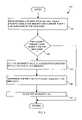
- FIG. 4shows a power sequencing procedure 110 which is suitable for use as step 104 in FIG. 3 .
- the packaged microcontroller 36receives, on the set of input lines 50 , a first set of power signals 40 which is provided by the power circuitry 32 to portions (e.g., the I/O buffers) of its respective storage processor 30 of the storage processing circuitry 24 (e.g., 3.3 VDC, 1.8 VDC, etc.).
- the packaged microcontroller 36receives compares the voltage levels of these power signals 40 to predetermined thresholds and proceeds to step 114 only after the power signals 40 have reached these thresholds.
- the control circuitry 54is capable of precisely measuring the particular voltage levels of these power signals 40 through the built-in A/D converters 52 .
- step 114the packaged microcontroller 36 waits a predetermined amount of time. This guarantees that the voltage levels of the power signals 40 have stabilized and that its respective storage processor 30 of the storage processing circuitry 24 which receives these power signals 40 (e.g., the I/O circuitry) is properly powered. Step 114 then proceeds to step 116 .
- the packaged microcontroller 36outputs, through the set of output lines 58 , a set of control signals 80 to the power circuitry 32 .
- These control signals 80(e.g., enable signals) directs the power circuitry 32 to provide a second set of power signals 40 to its respective storage processor 30 of the storage processing circuitry 24 (e.g., 2.5 VDC, 1.25 VDC, etc.).
- the packaged microcontroller 36is capable of determining that the second set of power signals 40 is properly provided by sensing through additional built-in A/D converters 52 in a feedback manner.
- portions of the storage processor 30 of the storage processing circuitry 24e.g., the core circuitry subsequently receives the remaining power signals 40 for robust and reliable operation due to receipt of the power signal 40 in proper sequence. Further details of the invention will now be provided with reference to FIG. 5 .
- FIG. 5shows an automated upgrade routine 120 which is performed by the package microcontroller 36 .
- the package microcontroller 36runs the automated upgrade routine 120 each time it establishes communication with its respective storage processor 30 through its data port 60 ( 1 ) (also see FIG. 1 ).
- Use of this automated upgrade routine 120enables the data storage system 20 to use the most recent version of operating code. Accordingly, modifications to the operation of the packaged microcontroller 36 (e.g., a change to the power sequencing procedure, bug fixes, enhancements, etc.) are easily made by simply providing accessibility to the new version of the code. No hardware changes (e.g., replacing components, running an external wire, etc.) are required as in conventional power sequencing circuits implemented with discrete components.
- step 122the packaged microcontroller 36 reads the version identifier 66 which stored with the pre-loaded primary code 66 stored in the portion 62 of the memory 56 with the version identifier 78 of the available new code 76 .
- the relative values of the version identifiers 66 , 78indicate whether the available new code 76 is more recent than the primary code 66 .
- step 124the packaged microcontroller 36 compares the version identifier 66 with the version identifier 78 . If the version identifier 66 indicates that the primary code 66 is at least as new as the available new code 78 (i.e., the version identifier 66 is equal to or more recent that the version identifier 78 ), the packaged microcontroller 36 skips steps 126 through 130 thus maintaining the pre-loaded primary code 64 within the memory 56 . Otherwise, if the version identifier 66 indicates that the primary code 66 is older than the available new code 76 , the packaged microcontroller proceeds to step 126 .
- step 126the packaged microcontroller 36 sets a dedicated upgrade flag (i.e., one of the memory locations 74 in the portion 72 of the memory 56 , also see FIG. 2 ) to indicate that the packaged microcontroller 36 is about to perform a code replacement routine to overwrite the primary code 64 .
- a dedicated upgrade flagi.e., one of the memory locations 74 in the portion 72 of the memory 56 , also see FIG. 2
- step 128the packaged microcontroller 36 replaces the pre-loaded primary code 64 and the version identifier 66 stored in the portion 62 of the memory 54 with the available new code 76 and the version identifier 78 .
- step 130the packaged microcontroller 36 clears the dedicated upgrade flag to indicate that the packaged microcontroller 36 is no longer overwriting the primary code 64 , i.e., that the code replacement routine is no longer in progress.
- the packaged microcontroller 36has built-in safeguards for fault tolerance purposes. For example, prior to attempting to access the primary code 64 in the memory 56 (e.g., when the user turns on the data storage system 20 , also see FIG. 3 ), the packaged microcontroller 36 checks to see whether an upgrade of the primary code 64 was inadvertently terminated before it completed. If an upgrade terminated before completing (e.g., due to loss of power), the upgrade flag in the portion 72 of the memory 56 will still be set when the packaged microcontroller 36 attempts to run the primary code 64 . In this situation, the packaged microcontroller 36 runs the boot block code 70 in the memory portion 68 rather than the primary code 64 . However, if the upgrade flag is clear, the packaged microcontroller 36 runs the primary code 64 as explained earlier.
- the boot block code 70operates as a backup in case the control circuitry 54 of the packaged microcontroller 36 cannot access the primary code 64 .
- This secondary boot block code 70is similar to the primary code 64 in that it properly power sequences the power signals 40 to prevent damage to the storage processors 30 of the data storage system 20 , but is a simpler version in that it does not include as full or robust a set of operations thus assuming that the data storage system 20 will undergo servicing.
- the boot block code 70is essentially code that the packaged microcontroller 36 runs as a failsafe if the packaged microcontroller 36 is unable to read the primary code 64 (e.g., if the primary code 64 is corrupted).
- each packaged microcontroller 36stores the ON/OFF state of its respective storage processor 30 in a persistent memory location, i.e., an ON/OFF flag in one of the memory locations 74 of the memory portion 72 .
- the packaged microcontroller 36updates the memory location by setting its ON/OFF flag to ON.
- the packaged microcontroller 36updates that memory location again by setting the ON/OFF flag to OFF.
- the packaged microcontroller 36when the packaged microcontroller 36 receives power, the packaged microcontroller 36 is capable of determining whether the user has toggled the ON/OFF switch, or whether main power has just returned after a loss of main power. In particular, when the packaged microcontroller 36 receives power (as part of step 102 in FIG. 3 ), the packaged microcontroller 36 reads the ON/OFF flag. If the ON/OFF flag is clear (i.e., the power button was last toggled to the OFF position by the user), the data storage system 20 had been in the OFF state and the user has just toggled the ON/OFF switch to turn on the data storage system 20 . As a result, the packaged microcontroller 36 performs the procedure 100 in a normal operating state as described above.
- the ON/OFF flagis set (i.e., the power button was last toggled to the ON position by the user)
- the data storage system 20had been in the ON state and main power has just returned thus enabling the data storage system 20 to enter a recovery state to perform a more extensive diagnostic and/or recovery routine to verify that no data has been lost and that no damage has occurred.
- each packaged microcontroller 36is capable of coordinating the ON/OFF state of its respective storage processor 30 with other storage processors 30 as well.
- each packaged microcontroller 36communicates with the other packaged microcontrollers 36 through the data port 60 ( 2 ) (e.g., through UARTs in a peer-to-peer manner) to make sure that its storage processors 30 as well as the other storage processors 30 are in synchronized states.
- the packaged microcontroller 36 for one storage processor 30has an ON state and the packaged microcontroller 36 for another storage processor 30 has an OFF state, the packaged microcontroller 36 in the OFF state turns to the ON state in order to synchronize its operation.
- This operationprevents the storage processors 30 from inadvertently attempting to operate in opposing manners, i.e., avoids one storage processor 30 trying to turn on while another storage processor 30 tries to turn off.
- embodiments of the inventionare directed to techniques for controlling a data storage system 20 having (i) a power subsystem 26 for providing power signals 40 and (ii) storage processing circuitry 24 for performing data storage operations, utilizing a packaged microcontroller 36 to control power sequencing.
- a power subsystem 26for providing power signals 40
- storage processing circuitry 24for performing data storage operations
- Such useprovides power sequencing at a relatively low cost (e.g., less components) and uses a relatively small amount of circuit board real estate (e.g., the footprint of the packaged microcontroller 36 ).
- a manufacturer of the data storage system 20is capable of easily modifying an initial power up sequence by providing new code 76 to the packaged microcontroller 36 .
- the manufactureris capable of programming the microcontroller 36 with more robust operations, e.g., automatic upgrading of boot code, utilization of interrupts to respond to particular events, coordination of multiple storage processors, etc.
- the data storage system 20was described above as having two storage processors 30 by way of example only. In other arrangements, the data storage system 20 has a different number of storage processors 30 (e.g., one, three, four, etc.).
- packaged microcontrollers 36communicated with their respective storage processors 30 through 12 C buses by way of example only.
- Other communications mediaare suitable for use as well, e.g., GPIO lines, UARTs, other available interfaces, etc.
Landscapes
- Engineering & Computer Science (AREA)
- Theoretical Computer Science (AREA)
- Physics & Mathematics (AREA)
- General Engineering & Computer Science (AREA)
- General Physics & Mathematics (AREA)
- Power Sources (AREA)
Abstract
Description
Claims (19)
Priority Applications (1)
| Application Number | Priority Date | Filing Date | Title |
|---|---|---|---|
| US10/810,431US7281150B1 (en) | 2004-03-26 | 2004-03-26 | Methods and apparatus for controlling operation of a data storage system |
Applications Claiming Priority (1)
| Application Number | Priority Date | Filing Date | Title |
|---|---|---|---|
| US10/810,431US7281150B1 (en) | 2004-03-26 | 2004-03-26 | Methods and apparatus for controlling operation of a data storage system |
Publications (1)
| Publication Number | Publication Date |
|---|---|
| US7281150B1true US7281150B1 (en) | 2007-10-09 |
Family
ID=38562261
Family Applications (1)
| Application Number | Title | Priority Date | Filing Date |
|---|---|---|---|
| US10/810,431Expired - LifetimeUS7281150B1 (en) | 2004-03-26 | 2004-03-26 | Methods and apparatus for controlling operation of a data storage system |
Country Status (1)
| Country | Link |
|---|---|
| US (1) | US7281150B1 (en) |
Cited By (10)
| Publication number | Priority date | Publication date | Assignee | Title |
|---|---|---|---|---|
| US20070101166A1 (en)* | 2005-10-31 | 2007-05-03 | Kevin Boyum | Method and apparatus for utilizing a microcontroller to provide an automatic order and timing power and reset sequencer |
| CN103150000A (en)* | 2011-12-07 | 2013-06-12 | 神讯电脑(昆山)有限公司 | Booting method for low temperature environment and electronic apparatus therefor |
| US20140219154A1 (en)* | 2011-09-06 | 2014-08-07 | Zte Corporation | Method for power-on control of mobile terminal and mobile terminal |
| US20150046724A1 (en)* | 2013-08-08 | 2015-02-12 | Lenovo (Beijing) Limited | Power supply methods and electronic devices |
| US9562188B2 (en) | 2013-09-20 | 2017-02-07 | Baker Hughes Incorporated | Composites for use in stimulation and sand control operations |
| US9683431B2 (en) | 2013-09-20 | 2017-06-20 | Baker Hughes Incorporated | Method of using surface modifying metallic treatment agents to treat subterranean formations |
| US9701892B2 (en) | 2014-04-17 | 2017-07-11 | Baker Hughes Incorporated | Method of pumping aqueous fluid containing surface modifying treatment agent into a well |
| US9822621B2 (en) | 2013-09-20 | 2017-11-21 | Baker Hughes, A Ge Company, Llc | Method of using surface modifying treatment agents to treat subterranean formations |
| US10047280B2 (en) | 2013-09-20 | 2018-08-14 | Baker Hughes, A Ge Company, Llc | Organophosphorus containing composites for use in well treatment operations |
| US10227846B2 (en) | 2013-09-20 | 2019-03-12 | Baker Hughes, A Ge Company, Llc | Method of inhibiting fouling on a metallic surface using a surface modifying treatment agent |
Citations (20)
| Publication number | Priority date | Publication date | Assignee | Title |
|---|---|---|---|---|
| US5339446A (en)* | 1986-12-26 | 1994-08-16 | Kabushiki Kaisha Toshiba | Power supply and method for use in a computer system to confirm a save operation of the computer system and to stop a supply of power to the computer system after confirmation |
| US6237103B1 (en)* | 1998-09-30 | 2001-05-22 | International Business Machines Corporation | Power sequencing in a data processing system |
| US6333650B1 (en)* | 2000-12-05 | 2001-12-25 | Juniper Networks, Inc. | Voltage sequencing circuit for powering-up sensitive electrical components |
| US6601176B1 (en)* | 1999-09-08 | 2003-07-29 | Visteon Global Technologies, Inc. | Automotive computer system and method whereby responsive to detecting engine cranking main processor enters a suspend mode and current state of devices are stored in volatile memory |
| US6633905B1 (en) | 1998-09-22 | 2003-10-14 | Avocent Huntsville Corporation | System and method for accessing and operating personal computers remotely |
| US6678639B2 (en) | 2000-08-04 | 2004-01-13 | Sun Microsystems, Inc. | Automated problem identification system |
| US6681282B1 (en) | 2000-08-31 | 2004-01-20 | Hewlett-Packard Development Company, L.P. | Online control of a multiprocessor computer system |
| US6735706B2 (en)* | 2000-12-06 | 2004-05-11 | Lattice Semiconductor Corporation | Programmable power management system and method |
| US6792553B2 (en)* | 2000-12-29 | 2004-09-14 | Hewlett-Packard Development Company, L.P. | CPU power sequence for large multiprocessor systems |
| US6850048B2 (en)* | 2003-05-02 | 2005-02-01 | Potentia Semiconductor, Inc. | Power supply controller |
| US6873268B2 (en) | 2000-01-21 | 2005-03-29 | Medtronic Minimed, Inc. | Microprocessor controlled ambulatory medical apparatus with hand held communication device |
| US6879139B2 (en)* | 2003-05-02 | 2005-04-12 | Potentia Semiconductor, Inc. | Sequencing power supplies |
| US6901572B1 (en)* | 2002-10-15 | 2005-05-31 | Lattice Semiconductor Corporation | Power sequence controller programming technique |
| US20050135069A1 (en) | 2003-12-22 | 2005-06-23 | Emc Corporation | Midplane-less data storage enclosure |
| US6924986B1 (en) | 2003-06-27 | 2005-08-02 | Emc Corporation | Invertible, pluggable module for variable I/O densities |
| US20050223284A1 (en) | 2004-03-25 | 2005-10-06 | Stephen Strickland | Techniques for maintaining operation of data storage system during a failure |
| US7039737B1 (en) | 2003-12-12 | 2006-05-02 | Emc Corporation | Method and apparatus for resource arbitration |
| US7080273B2 (en)* | 2003-05-02 | 2006-07-18 | Potentia Semiconductor, Inc. | Sequencing power supplies on daughter boards |
| US7080264B2 (en)* | 2002-12-11 | 2006-07-18 | Sun Microsystems, Inc. | Methods and apparatus for providing microprocessor firmware control of power sequencing on a CPCI card |
| US7111183B1 (en)* | 2002-10-10 | 2006-09-19 | Lattice Semiconductor Corporation | Expansion method for complex power-sequencing applications |
- 2004
- 2004-03-26USUS10/810,431patent/US7281150B1/ennot_activeExpired - Lifetime
Patent Citations (22)
| Publication number | Priority date | Publication date | Assignee | Title |
|---|---|---|---|---|
| US5339446A (en)* | 1986-12-26 | 1994-08-16 | Kabushiki Kaisha Toshiba | Power supply and method for use in a computer system to confirm a save operation of the computer system and to stop a supply of power to the computer system after confirmation |
| US6633905B1 (en) | 1998-09-22 | 2003-10-14 | Avocent Huntsville Corporation | System and method for accessing and operating personal computers remotely |
| US6237103B1 (en)* | 1998-09-30 | 2001-05-22 | International Business Machines Corporation | Power sequencing in a data processing system |
| US6601176B1 (en)* | 1999-09-08 | 2003-07-29 | Visteon Global Technologies, Inc. | Automotive computer system and method whereby responsive to detecting engine cranking main processor enters a suspend mode and current state of devices are stored in volatile memory |
| US6873268B2 (en) | 2000-01-21 | 2005-03-29 | Medtronic Minimed, Inc. | Microprocessor controlled ambulatory medical apparatus with hand held communication device |
| US6678639B2 (en) | 2000-08-04 | 2004-01-13 | Sun Microsystems, Inc. | Automated problem identification system |
| US6681282B1 (en) | 2000-08-31 | 2004-01-20 | Hewlett-Packard Development Company, L.P. | Online control of a multiprocessor computer system |
| US6429706B1 (en)* | 2000-12-05 | 2002-08-06 | Juniper Networks, Inc. | Voltage sequencing circuit for powering-up sensitive electrical components |
| US6333650B1 (en)* | 2000-12-05 | 2001-12-25 | Juniper Networks, Inc. | Voltage sequencing circuit for powering-up sensitive electrical components |
| US6735706B2 (en)* | 2000-12-06 | 2004-05-11 | Lattice Semiconductor Corporation | Programmable power management system and method |
| US7100058B1 (en)* | 2000-12-06 | 2006-08-29 | Lattice Semiconductor Corporation | Programmable power management system and method |
| US6792553B2 (en)* | 2000-12-29 | 2004-09-14 | Hewlett-Packard Development Company, L.P. | CPU power sequence for large multiprocessor systems |
| US7111183B1 (en)* | 2002-10-10 | 2006-09-19 | Lattice Semiconductor Corporation | Expansion method for complex power-sequencing applications |
| US6901572B1 (en)* | 2002-10-15 | 2005-05-31 | Lattice Semiconductor Corporation | Power sequence controller programming technique |
| US7080264B2 (en)* | 2002-12-11 | 2006-07-18 | Sun Microsystems, Inc. | Methods and apparatus for providing microprocessor firmware control of power sequencing on a CPCI card |
| US6850048B2 (en)* | 2003-05-02 | 2005-02-01 | Potentia Semiconductor, Inc. | Power supply controller |
| US7080273B2 (en)* | 2003-05-02 | 2006-07-18 | Potentia Semiconductor, Inc. | Sequencing power supplies on daughter boards |
| US6879139B2 (en)* | 2003-05-02 | 2005-04-12 | Potentia Semiconductor, Inc. | Sequencing power supplies |
| US6924986B1 (en) | 2003-06-27 | 2005-08-02 | Emc Corporation | Invertible, pluggable module for variable I/O densities |
| US7039737B1 (en) | 2003-12-12 | 2006-05-02 | Emc Corporation | Method and apparatus for resource arbitration |
| US20050135069A1 (en) | 2003-12-22 | 2005-06-23 | Emc Corporation | Midplane-less data storage enclosure |
| US20050223284A1 (en) | 2004-03-25 | 2005-10-06 | Stephen Strickland | Techniques for maintaining operation of data storage system during a failure |
Cited By (15)
| Publication number | Priority date | Publication date | Assignee | Title |
|---|---|---|---|---|
| US7613937B2 (en)* | 2005-10-31 | 2009-11-03 | Hewlett-Packard Development Company, L.P. | Method and apparatus for utilizing a microcontroller to provide an automatic order and timing power and reset sequencer |
| US20070101166A1 (en)* | 2005-10-31 | 2007-05-03 | Kevin Boyum | Method and apparatus for utilizing a microcontroller to provide an automatic order and timing power and reset sequencer |
| US20140219154A1 (en)* | 2011-09-06 | 2014-08-07 | Zte Corporation | Method for power-on control of mobile terminal and mobile terminal |
| US9781682B2 (en)* | 2011-09-06 | 2017-10-03 | Xi'an Zte New Software Company Limited | Method for power-on control of mobile terminal |
| US8972709B2 (en)* | 2011-12-07 | 2015-03-03 | Getac Technology Corporation | Booting method for low temperature environment and electronic apparatus therefor |
| US20130151833A1 (en)* | 2011-12-07 | 2013-06-13 | Getac Technology Corporation | Booting method for low temperature environment and electronic apparatus therefor |
| CN103150000B (en)* | 2011-12-07 | 2016-01-20 | 神讯电脑(昆山)有限公司 | Low temperature starting-up method and electronic installation thereof |
| CN103150000A (en)* | 2011-12-07 | 2013-06-12 | 神讯电脑(昆山)有限公司 | Booting method for low temperature environment and electronic apparatus therefor |
| US20150046724A1 (en)* | 2013-08-08 | 2015-02-12 | Lenovo (Beijing) Limited | Power supply methods and electronic devices |
| US9562188B2 (en) | 2013-09-20 | 2017-02-07 | Baker Hughes Incorporated | Composites for use in stimulation and sand control operations |
| US9683431B2 (en) | 2013-09-20 | 2017-06-20 | Baker Hughes Incorporated | Method of using surface modifying metallic treatment agents to treat subterranean formations |
| US9822621B2 (en) | 2013-09-20 | 2017-11-21 | Baker Hughes, A Ge Company, Llc | Method of using surface modifying treatment agents to treat subterranean formations |
| US10047280B2 (en) | 2013-09-20 | 2018-08-14 | Baker Hughes, A Ge Company, Llc | Organophosphorus containing composites for use in well treatment operations |
| US10227846B2 (en) | 2013-09-20 | 2019-03-12 | Baker Hughes, A Ge Company, Llc | Method of inhibiting fouling on a metallic surface using a surface modifying treatment agent |
| US9701892B2 (en) | 2014-04-17 | 2017-07-11 | Baker Hughes Incorporated | Method of pumping aqueous fluid containing surface modifying treatment agent into a well |
Similar Documents
| Publication | Publication Date | Title |
|---|---|---|
| EP0992000B1 (en) | Bus interface system and method | |
| US7234050B2 (en) | Techniques for initializing a device on an expansion card | |
| EP0698240B1 (en) | Apparatus and method for automatic recognition and configuration of a peripheral device | |
| US5805882A (en) | Computer system and method for replacing obsolete or corrupt boot code contained within reprogrammable memory with new boot code supplied from an external source through a data port | |
| US7631174B2 (en) | Method of updating firmware in computer server systems | |
| CA1335843C (en) | Programmable option select | |
| US20040083469A1 (en) | Method for updating firmware of optical disk system | |
| US20140163716A1 (en) | Bridge device, automated production system and method thereof for storage device | |
| US7822964B2 (en) | Booting apparatus for booting a computer and method therefor and computer with a booting apparatus | |
| US7281150B1 (en) | Methods and apparatus for controlling operation of a data storage system | |
| CN101593120A (en) | Be with outer upgrade method and system | |
| US7613937B2 (en) | Method and apparatus for utilizing a microcontroller to provide an automatic order and timing power and reset sequencer | |
| US6530005B2 (en) | Circuit arrangement and method for creating and retrieving patch data from memory | |
| US20060184763A1 (en) | System and method for updating firmware in a non-volatile memory without using a processor | |
| US7111160B1 (en) | Method and apparatus for using a development port for boot up | |
| JP7273176B2 (en) | Memory control system with sequence processing unit | |
| US7076643B2 (en) | Method and apparatus for providing revision identification numbers | |
| EP0574991A1 (en) | A data processing system adaptable to the type of microprocessor installed and method for detecting the microprocessor type | |
| US6466994B1 (en) | Method and system for programming a system board using a peripheral controller | |
| US6622245B1 (en) | Firmware field programming interface and module for programming non-volatile memory on a circuit board while isolating the processor from power using expansion bus controller | |
| CN111414323B (en) | Redundant bundle disk | |
| US20040255178A1 (en) | Micro-system for burn-in system program from a plug-able subsystem into main memory and method thereof | |
| US8650366B2 (en) | Memory system capable of enhancing writing protection and related method | |
| CN116913363A (en) | Method for identifying and isolating DIMMs with power failure | |
| US20210141627A1 (en) | Power delivery controller updates |
Legal Events
| Date | Code | Title | Description |
|---|---|---|---|
| AS | Assignment | Owner name:EMC CORPORATION, MASSACHUSETTS Free format text:ASSIGNMENT OF ASSIGNORS INTEREST;ASSIGNOR:STRICKLAND, STEPHEN;REEL/FRAME:015157/0908 Effective date:20040325 | |
| STCF | Information on status: patent grant | Free format text:PATENTED CASE | |
| FEPP | Fee payment procedure | Free format text:PAYOR NUMBER ASSIGNED (ORIGINAL EVENT CODE: ASPN); ENTITY STATUS OF PATENT OWNER: LARGE ENTITY | |
| FPAY | Fee payment | Year of fee payment:4 | |
| FPAY | Fee payment | Year of fee payment:8 | |
| FPAY | Fee payment | Year of fee payment:8 | |
| SULP | Surcharge for late payment | Year of fee payment:7 | |
| AS | Assignment | Owner name:THE BANK OF NEW YORK MELLON TRUST COMPANY, N.A., AS NOTES COLLATERAL AGENT, TEXAS Free format text:SECURITY AGREEMENT;ASSIGNORS:ASAP SOFTWARE EXPRESS, INC.;AVENTAIL LLC;CREDANT TECHNOLOGIES, INC.;AND OTHERS;REEL/FRAME:040136/0001 Effective date:20160907 Owner name:CREDIT SUISSE AG, CAYMAN ISLANDS BRANCH, AS COLLATERAL AGENT, NORTH CAROLINA Free format text:SECURITY AGREEMENT;ASSIGNORS:ASAP SOFTWARE EXPRESS, INC.;AVENTAIL LLC;CREDANT TECHNOLOGIES, INC.;AND OTHERS;REEL/FRAME:040134/0001 Effective date:20160907 Owner name:CREDIT SUISSE AG, CAYMAN ISLANDS BRANCH, AS COLLAT Free format text:SECURITY AGREEMENT;ASSIGNORS:ASAP SOFTWARE EXPRESS, INC.;AVENTAIL LLC;CREDANT TECHNOLOGIES, INC.;AND OTHERS;REEL/FRAME:040134/0001 Effective date:20160907 Owner name:THE BANK OF NEW YORK MELLON TRUST COMPANY, N.A., A Free format text:SECURITY AGREEMENT;ASSIGNORS:ASAP SOFTWARE EXPRESS, INC.;AVENTAIL LLC;CREDANT TECHNOLOGIES, INC.;AND OTHERS;REEL/FRAME:040136/0001 Effective date:20160907 | |
| AS | Assignment | Owner name:EMC IP HOLDING COMPANY LLC, MASSACHUSETTS Free format text:ASSIGNMENT OF ASSIGNORS INTEREST;ASSIGNOR:EMC CORPORATION;REEL/FRAME:040203/0001 Effective date:20160906 | |
| AS | Assignment | Owner name:THE BANK OF NEW YORK MELLON TRUST COMPANY, N.A., T Free format text:SECURITY AGREEMENT;ASSIGNORS:CREDANT TECHNOLOGIES, INC.;DELL INTERNATIONAL L.L.C.;DELL MARKETING L.P.;AND OTHERS;REEL/FRAME:049452/0223 Effective date:20190320 Owner name:THE BANK OF NEW YORK MELLON TRUST COMPANY, N.A., TEXAS Free format text:SECURITY AGREEMENT;ASSIGNORS:CREDANT TECHNOLOGIES, INC.;DELL INTERNATIONAL L.L.C.;DELL MARKETING L.P.;AND OTHERS;REEL/FRAME:049452/0223 Effective date:20190320 | |
| MAFP | Maintenance fee payment | Free format text:PAYMENT OF MAINTENANCE FEE, 12TH YEAR, LARGE ENTITY (ORIGINAL EVENT CODE: M1553); ENTITY STATUS OF PATENT OWNER: LARGE ENTITY Year of fee payment:12 | |
| AS | Assignment | Owner name:THE BANK OF NEW YORK MELLON TRUST COMPANY, N.A., TEXAS Free format text:SECURITY AGREEMENT;ASSIGNORS:CREDANT TECHNOLOGIES INC.;DELL INTERNATIONAL L.L.C.;DELL MARKETING L.P.;AND OTHERS;REEL/FRAME:053546/0001 Effective date:20200409 | |
| AS | Assignment | Owner name:WYSE TECHNOLOGY L.L.C., CALIFORNIA Free format text:RELEASE BY SECURED PARTY;ASSIGNOR:CREDIT SUISSE AG, CAYMAN ISLANDS BRANCH;REEL/FRAME:058216/0001 Effective date:20211101 Owner name:SCALEIO LLC, MASSACHUSETTS Free format text:RELEASE BY SECURED PARTY;ASSIGNOR:CREDIT SUISSE AG, CAYMAN ISLANDS BRANCH;REEL/FRAME:058216/0001 Effective date:20211101 Owner name:MOZY, INC., WASHINGTON Free format text:RELEASE BY SECURED PARTY;ASSIGNOR:CREDIT SUISSE AG, CAYMAN ISLANDS BRANCH;REEL/FRAME:058216/0001 Effective date:20211101 Owner name:MAGINATICS LLC, CALIFORNIA Free format text:RELEASE BY SECURED PARTY;ASSIGNOR:CREDIT SUISSE AG, CAYMAN ISLANDS BRANCH;REEL/FRAME:058216/0001 Effective date:20211101 Owner name:FORCE10 NETWORKS, INC., CALIFORNIA Free format text:RELEASE BY SECURED PARTY;ASSIGNOR:CREDIT SUISSE AG, CAYMAN ISLANDS BRANCH;REEL/FRAME:058216/0001 Effective date:20211101 Owner name:EMC IP HOLDING COMPANY LLC, TEXAS Free format text:RELEASE BY SECURED PARTY;ASSIGNOR:CREDIT SUISSE AG, CAYMAN ISLANDS BRANCH;REEL/FRAME:058216/0001 Effective date:20211101 Owner name:EMC CORPORATION, MASSACHUSETTS Free format text:RELEASE BY SECURED PARTY;ASSIGNOR:CREDIT SUISSE AG, CAYMAN ISLANDS BRANCH;REEL/FRAME:058216/0001 Effective date:20211101 Owner name:DELL SYSTEMS CORPORATION, TEXAS Free format text:RELEASE BY SECURED PARTY;ASSIGNOR:CREDIT SUISSE AG, CAYMAN ISLANDS BRANCH;REEL/FRAME:058216/0001 Effective date:20211101 Owner name:DELL SOFTWARE INC., CALIFORNIA Free format text:RELEASE BY SECURED PARTY;ASSIGNOR:CREDIT SUISSE AG, CAYMAN ISLANDS BRANCH;REEL/FRAME:058216/0001 Effective date:20211101 Owner name:DELL PRODUCTS L.P., TEXAS Free format text:RELEASE BY SECURED PARTY;ASSIGNOR:CREDIT SUISSE AG, CAYMAN ISLANDS BRANCH;REEL/FRAME:058216/0001 Effective date:20211101 Owner name:DELL MARKETING L.P., TEXAS Free format text:RELEASE BY SECURED PARTY;ASSIGNOR:CREDIT SUISSE AG, CAYMAN ISLANDS BRANCH;REEL/FRAME:058216/0001 Effective date:20211101 Owner name:DELL INTERNATIONAL, L.L.C., TEXAS Free format text:RELEASE BY SECURED PARTY;ASSIGNOR:CREDIT SUISSE AG, CAYMAN ISLANDS BRANCH;REEL/FRAME:058216/0001 Effective date:20211101 Owner name:DELL USA L.P., TEXAS Free format text:RELEASE BY SECURED PARTY;ASSIGNOR:CREDIT SUISSE AG, CAYMAN ISLANDS BRANCH;REEL/FRAME:058216/0001 Effective date:20211101 Owner name:CREDANT TECHNOLOGIES, INC., TEXAS Free format text:RELEASE BY SECURED PARTY;ASSIGNOR:CREDIT SUISSE AG, CAYMAN ISLANDS BRANCH;REEL/FRAME:058216/0001 Effective date:20211101 Owner name:AVENTAIL LLC, CALIFORNIA Free format text:RELEASE BY SECURED PARTY;ASSIGNOR:CREDIT SUISSE AG, CAYMAN ISLANDS BRANCH;REEL/FRAME:058216/0001 Effective date:20211101 Owner name:ASAP SOFTWARE EXPRESS, INC., ILLINOIS Free format text:RELEASE BY SECURED PARTY;ASSIGNOR:CREDIT SUISSE AG, CAYMAN ISLANDS BRANCH;REEL/FRAME:058216/0001 Effective date:20211101 | |
| AS | Assignment | Owner name:SCALEIO LLC, MASSACHUSETTS Free format text:RELEASE OF SECURITY INTEREST IN PATENTS PREVIOUSLY RECORDED AT REEL/FRAME (040136/0001);ASSIGNOR:THE BANK OF NEW YORK MELLON TRUST COMPANY, N.A., AS NOTES COLLATERAL AGENT;REEL/FRAME:061324/0001 Effective date:20220329 Owner name:EMC IP HOLDING COMPANY LLC (ON BEHALF OF ITSELF AND AS SUCCESSOR-IN-INTEREST TO MOZY, INC.), TEXAS Free format text:RELEASE OF SECURITY INTEREST IN PATENTS PREVIOUSLY RECORDED AT REEL/FRAME (040136/0001);ASSIGNOR:THE BANK OF NEW YORK MELLON TRUST COMPANY, N.A., AS NOTES COLLATERAL AGENT;REEL/FRAME:061324/0001 Effective date:20220329 Owner name:EMC CORPORATION (ON BEHALF OF ITSELF AND AS SUCCESSOR-IN-INTEREST TO MAGINATICS LLC), MASSACHUSETTS Free format text:RELEASE OF SECURITY INTEREST IN PATENTS PREVIOUSLY RECORDED AT REEL/FRAME (040136/0001);ASSIGNOR:THE BANK OF NEW YORK MELLON TRUST COMPANY, N.A., AS NOTES COLLATERAL AGENT;REEL/FRAME:061324/0001 Effective date:20220329 Owner name:DELL MARKETING CORPORATION (SUCCESSOR-IN-INTEREST TO FORCE10 NETWORKS, INC. AND WYSE TECHNOLOGY L.L.C.), TEXAS Free format text:RELEASE OF SECURITY INTEREST IN PATENTS PREVIOUSLY RECORDED AT REEL/FRAME (040136/0001);ASSIGNOR:THE BANK OF NEW YORK MELLON TRUST COMPANY, N.A., AS NOTES COLLATERAL AGENT;REEL/FRAME:061324/0001 Effective date:20220329 Owner name:DELL PRODUCTS L.P., TEXAS Free format text:RELEASE OF SECURITY INTEREST IN PATENTS PREVIOUSLY RECORDED AT REEL/FRAME (040136/0001);ASSIGNOR:THE BANK OF NEW YORK MELLON TRUST COMPANY, N.A., AS NOTES COLLATERAL AGENT;REEL/FRAME:061324/0001 Effective date:20220329 Owner name:DELL INTERNATIONAL L.L.C., TEXAS Free format text:RELEASE OF SECURITY INTEREST IN PATENTS PREVIOUSLY RECORDED AT REEL/FRAME (040136/0001);ASSIGNOR:THE BANK OF NEW YORK MELLON TRUST COMPANY, N.A., AS NOTES COLLATERAL AGENT;REEL/FRAME:061324/0001 Effective date:20220329 Owner name:DELL USA L.P., TEXAS Free format text:RELEASE OF SECURITY INTEREST IN PATENTS PREVIOUSLY RECORDED AT REEL/FRAME (040136/0001);ASSIGNOR:THE BANK OF NEW YORK MELLON TRUST COMPANY, N.A., AS NOTES COLLATERAL AGENT;REEL/FRAME:061324/0001 Effective date:20220329 Owner name:DELL MARKETING L.P. (ON BEHALF OF ITSELF AND AS SUCCESSOR-IN-INTEREST TO CREDANT TECHNOLOGIES, INC.), TEXAS Free format text:RELEASE OF SECURITY INTEREST IN PATENTS PREVIOUSLY RECORDED AT REEL/FRAME (040136/0001);ASSIGNOR:THE BANK OF NEW YORK MELLON TRUST COMPANY, N.A., AS NOTES COLLATERAL AGENT;REEL/FRAME:061324/0001 Effective date:20220329 Owner name:DELL MARKETING CORPORATION (SUCCESSOR-IN-INTEREST TO ASAP SOFTWARE EXPRESS, INC.), TEXAS Free format text:RELEASE OF SECURITY INTEREST IN PATENTS PREVIOUSLY RECORDED AT REEL/FRAME (040136/0001);ASSIGNOR:THE BANK OF NEW YORK MELLON TRUST COMPANY, N.A., AS NOTES COLLATERAL AGENT;REEL/FRAME:061324/0001 Effective date:20220329 | |
| AS | Assignment | Owner name:SCALEIO LLC, MASSACHUSETTS Free format text:RELEASE OF SECURITY INTEREST IN PATENTS PREVIOUSLY RECORDED AT REEL/FRAME (045455/0001);ASSIGNOR:THE BANK OF NEW YORK MELLON TRUST COMPANY, N.A., AS NOTES COLLATERAL AGENT;REEL/FRAME:061753/0001 Effective date:20220329 Owner name:EMC IP HOLDING COMPANY LLC (ON BEHALF OF ITSELF AND AS SUCCESSOR-IN-INTEREST TO MOZY, INC.), TEXAS Free format text:RELEASE OF SECURITY INTEREST IN PATENTS PREVIOUSLY RECORDED AT REEL/FRAME (045455/0001);ASSIGNOR:THE BANK OF NEW YORK MELLON TRUST COMPANY, N.A., AS NOTES COLLATERAL AGENT;REEL/FRAME:061753/0001 Effective date:20220329 Owner name:EMC CORPORATION (ON BEHALF OF ITSELF AND AS SUCCESSOR-IN-INTEREST TO MAGINATICS LLC), MASSACHUSETTS Free format text:RELEASE OF SECURITY INTEREST IN PATENTS PREVIOUSLY RECORDED AT REEL/FRAME (045455/0001);ASSIGNOR:THE BANK OF NEW YORK MELLON TRUST COMPANY, N.A., AS NOTES COLLATERAL AGENT;REEL/FRAME:061753/0001 Effective date:20220329 Owner name:DELL MARKETING CORPORATION (SUCCESSOR-IN-INTEREST TO FORCE10 NETWORKS, INC. AND WYSE TECHNOLOGY L.L.C.), TEXAS Free format text:RELEASE OF SECURITY INTEREST IN PATENTS PREVIOUSLY RECORDED AT REEL/FRAME (045455/0001);ASSIGNOR:THE BANK OF NEW YORK MELLON TRUST COMPANY, N.A., AS NOTES COLLATERAL AGENT;REEL/FRAME:061753/0001 Effective date:20220329 Owner name:DELL PRODUCTS L.P., TEXAS Free format text:RELEASE OF SECURITY INTEREST IN PATENTS PREVIOUSLY RECORDED AT REEL/FRAME (045455/0001);ASSIGNOR:THE BANK OF NEW YORK MELLON TRUST COMPANY, N.A., AS NOTES COLLATERAL AGENT;REEL/FRAME:061753/0001 Effective date:20220329 Owner name:DELL INTERNATIONAL L.L.C., TEXAS Free format text:RELEASE OF SECURITY INTEREST IN PATENTS PREVIOUSLY RECORDED AT REEL/FRAME (045455/0001);ASSIGNOR:THE BANK OF NEW YORK MELLON TRUST COMPANY, N.A., AS NOTES COLLATERAL AGENT;REEL/FRAME:061753/0001 Effective date:20220329 Owner name:DELL USA L.P., TEXAS Free format text:RELEASE OF SECURITY INTEREST IN PATENTS PREVIOUSLY RECORDED AT REEL/FRAME (045455/0001);ASSIGNOR:THE BANK OF NEW YORK MELLON TRUST COMPANY, N.A., AS NOTES COLLATERAL AGENT;REEL/FRAME:061753/0001 Effective date:20220329 Owner name:DELL MARKETING L.P. (ON BEHALF OF ITSELF AND AS SUCCESSOR-IN-INTEREST TO CREDANT TECHNOLOGIES, INC.), TEXAS Free format text:RELEASE OF SECURITY INTEREST IN PATENTS PREVIOUSLY RECORDED AT REEL/FRAME (045455/0001);ASSIGNOR:THE BANK OF NEW YORK MELLON TRUST COMPANY, N.A., AS NOTES COLLATERAL AGENT;REEL/FRAME:061753/0001 Effective date:20220329 Owner name:DELL MARKETING CORPORATION (SUCCESSOR-IN-INTEREST TO ASAP SOFTWARE EXPRESS, INC.), TEXAS Free format text:RELEASE OF SECURITY INTEREST IN PATENTS PREVIOUSLY RECORDED AT REEL/FRAME (045455/0001);ASSIGNOR:THE BANK OF NEW YORK MELLON TRUST COMPANY, N.A., AS NOTES COLLATERAL AGENT;REEL/FRAME:061753/0001 Effective date:20220329 | |
| AS | Assignment | Owner name:DELL MARKETING L.P. (ON BEHALF OF ITSELF AND AS SUCCESSOR-IN-INTEREST TO CREDANT TECHNOLOGIES, INC.), TEXAS Free format text:RELEASE OF SECURITY INTEREST IN PATENTS PREVIOUSLY RECORDED AT REEL/FRAME (053546/0001);ASSIGNOR:THE BANK OF NEW YORK MELLON TRUST COMPANY, N.A., AS NOTES COLLATERAL AGENT;REEL/FRAME:071642/0001 Effective date:20220329 Owner name:DELL INTERNATIONAL L.L.C., TEXAS Free format text:RELEASE OF SECURITY INTEREST IN PATENTS PREVIOUSLY RECORDED AT REEL/FRAME (053546/0001);ASSIGNOR:THE BANK OF NEW YORK MELLON TRUST COMPANY, N.A., AS NOTES COLLATERAL AGENT;REEL/FRAME:071642/0001 Effective date:20220329 Owner name:DELL PRODUCTS L.P., TEXAS Free format text:RELEASE OF SECURITY INTEREST IN PATENTS PREVIOUSLY RECORDED AT REEL/FRAME (053546/0001);ASSIGNOR:THE BANK OF NEW YORK MELLON TRUST COMPANY, N.A., AS NOTES COLLATERAL AGENT;REEL/FRAME:071642/0001 Effective date:20220329 Owner name:DELL USA L.P., TEXAS Free format text:RELEASE OF SECURITY INTEREST IN PATENTS PREVIOUSLY RECORDED AT REEL/FRAME (053546/0001);ASSIGNOR:THE BANK OF NEW YORK MELLON TRUST COMPANY, N.A., AS NOTES COLLATERAL AGENT;REEL/FRAME:071642/0001 Effective date:20220329 Owner name:EMC CORPORATION, MASSACHUSETTS Free format text:RELEASE OF SECURITY INTEREST IN PATENTS PREVIOUSLY RECORDED AT REEL/FRAME (053546/0001);ASSIGNOR:THE BANK OF NEW YORK MELLON TRUST COMPANY, N.A., AS NOTES COLLATERAL AGENT;REEL/FRAME:071642/0001 Effective date:20220329 Owner name:DELL MARKETING CORPORATION (SUCCESSOR-IN-INTEREST TO FORCE10 NETWORKS, INC. AND WYSE TECHNOLOGY L.L.C.), TEXAS Free format text:RELEASE OF SECURITY INTEREST IN PATENTS PREVIOUSLY RECORDED AT REEL/FRAME (053546/0001);ASSIGNOR:THE BANK OF NEW YORK MELLON TRUST COMPANY, N.A., AS NOTES COLLATERAL AGENT;REEL/FRAME:071642/0001 Effective date:20220329 Owner name:EMC IP HOLDING COMPANY LLC, TEXAS Free format text:RELEASE OF SECURITY INTEREST IN PATENTS PREVIOUSLY RECORDED AT REEL/FRAME (053546/0001);ASSIGNOR:THE BANK OF NEW YORK MELLON TRUST COMPANY, N.A., AS NOTES COLLATERAL AGENT;REEL/FRAME:071642/0001 Effective date:20220329 |